1
State-Based Power Analysis for Systems-on-Chip
Reinaldo A. Bergamaschi
Yunjian W. Jiang
IBM T. J. Watson Research Center Yorktown
Heights, NY, USA
University of California
Berkeley, CA, USA
ABSTRACT
Early power analysis for systems-on-chip (SoC) is crucial for determining the appropriate packaging and cost. This early analysis commonly relies on evaluating power formulas for all cores for
multiple configurations of voltage, frequency, technology and application parameters, which is a tedious and error-prone process.
This work presents a methodology and algorithms for automating
the power analysis of SoCs. Given the power state machines for individual cores, this work defines the product power state machine
for the whole SoC and uses formal symbolic simulation algorithms
for traversing and computing the minimum and maximum power
dissipated by sets of power states in the SoC.
Categories and Subject Descriptors
J.6 [Computer-aided design]; B7.2 [Integrated circuits]: Design
aids
General Terms
Algorithms
Keywords
Power analysis, systems-on-chip, state exploration
1.
INTRODUCTION
In current systems-on-chip (SoC) design methodologies, one of
the first steps is the definition of the overall architecture and the
cost metrics, such as die-size, input/output (IO) requirements and
power consumption. These metrics are required for choosing the
appropriate packaging and define the overall dollar cost[1]. Since
this is done in the earliest stages of the design, there is no detailed
description, and the only available hardware specification is likely
to be a block diagram, with a list of components, and IO requirements.
Estimates of power consumption, at this stage, are based on
spreadsheets built from simplified power formulas. These formulas
are meant to return average power consumption values for given
estimated parameters, such as the size and type of the logic block,
capacitances, switching activity, number of hardware accesses, frequency and power supply (Vdd). Although these formulas can
be inaccurate, they can be tuned from design to design and with
enough designer experience on choosing the expected switching
activity for each block, they do provide useful early estimates for
the overall chip power consumption. The PowerPlay tool[2] is an
application of such spreadsheet approach.
Modern SoCs rely on power management schemes to control
power consumption dynamically. Power management approaches
Permission to make digital or hard copies of all or part of this work for
personal or classroom use is granted without fee provided that copies are
not made or distributed for profit or commercial advantage and that copies
bear this notice and the full citation on the first page. To copy otherwise, to
republish, to post on servers or to redistribute to lists, requires prior specific
permission and/or a fee.
DAC 2003, June 2–6, 2003, Anaheim, California, USA.
Copyright 2003 ACM 1-58113-688-9/03/0006 ...$5.00.
can be implemented in hardware and software by using a dedicated
power management unit (PMU) which can control the operational
modes of other cores. The PowerPC 603e processor [3], for example, supports four power modes, namely, Full Power, Doze, Nap
and Sleep. Other less complex cores may support simpler modes
such as Active for full operation, Idle for the no-input-activity state,
and Sleep for the fully clock-gated state. In an SoC, at any time
during its operation, there may be cores which are in active mode,
while others may be in sleep or other modes. By adding up the
power values for all cores according to their mode of operation,
one can get a value for the total SoC power consumption.
Given all variations in the power consumed by a core, a designer
is forced to run the spreadsheets hundreds of times for all cores with
different parameters in order to get a representative picture of the
SoC power consumption under different operating scenarios. This
is clearly very time consuming and error prone on the expected coverage. It is easy to overlook specific scenarios and fail to explore
fully the power design space when running the spreadsheet analysis
manually.
The work in [4] was a step in automating this process by modeling the different power modes in each core as a power state machine
(PSM) and applying a simulation of all state machines in order to
estimate the chip power for a given execution scenario. However,
this model was limited in that it did not take into account the interactions among the state machines and it required real input traces
to drive the simulation.
This paper presents an approach for early formal analysis and
exploration of the power design space for core-based SoCs. The
key to this analysis is a new formal model for the different states
in which the SoC can operate. Given the PSM for each core, the
approach in this paper computes the power state machine for the
whole SoC as the product of all individual PSMs for the cores. It
combines the spreadsheet-like calculations with the PSM model for
each core, and formally computes the product power state machine
for the whole SoC. It then performs a symbolic simulation of the
product PSM for all possible input combinations or for specific scenarios. To the best of the authors’ knowledge this is the first work
that applies formal methods to the dynamic analysis of power consumption in core-based SoCs.
2. CORE POWER STATE MACHINES
The power modes of each core are modeled as a PSM similar to
the one defined in [4], with the addition of output sets to model the
interactions among PSMs.
For the purposes of this paper three types of power models for
cores are considered, namely: class-0, class-1 and class-2. The
differences between them are related to how the power modes are
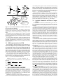
controlled. Figure 1(a) shows the PSMs for class-0, class-1 and
class-2 cores.
In these three classes, the Active state is the full operational
mode, the Idle state represents the low-activity state (core is not being accessed, no significant switching at the inputs), and the Sleep
state is the fully clock-gated state. The transitions between Active
and Idle states are not directly controlled by the PMU, but depend
on the environment (i.e., signal changes at the core inputs). In the
class-1 PSM in Figure 1(a), when signal Active is 0, it indicates
that the core is not being accessed and therefore can go to Idle.
While in Idle, if the PMU sends a Sleep signal the registers will be
clock-gated and the core will transition to Sleep state.
A core PSM may also have output signals which can be used to
a)
Active
Active / Timer_Start
Active
A
Active
A
A
I
Active
Active
Active
Active
Sleep
I
Active . Sleep
Active
Active
I
Q
Timer_Up /
Sleep_Req
Active . Sleep
Sleep
Sleep
Active
Active / Sleep_Req
S
Class I
Class 0
S
Class II
Sleep
Sleep
b)
Core1=Idle; Core2=Idle;
Core3=Idle; Core4=Idle;
Core5=Sleep; Core6=Sleep;
Core7=Sleep; ......
Init
S3
S1
S2
S8
S4
S5
S6
S7
Core1=Active; Core2=Active;
Core3=Active; Core4=Sleep;
Core5=Idle; Core6=Active;
Core7=Active; ......
Figure 1: a) Power-State machines for Class-0, I and II cores,
b) SoC Product State Machine
model interactions between PSMs. For example, a master device
accessing a bus can generate an output (in the PSM model) which
triggers activity in the bus arbiter PSM (e.g, asserting its Active
input).
Note that the power state machine may not directly correspond
to any physical state-machine implementation, but it is primarily an
abstraction of the different power consumption modes in which the
core can operate.
A sum-of-products based format, similar to the SHIFT format in
the Polis project [5], is used for specifying the transition function of
each PSM. The PSM file also specifies the core’s power consumption function and its parameters, such as switching activity ratio,
frequency, Vdd, etc.
2.1 BDD representation of a PSM
Since the PSM is a small state machine, it can be efficiently represented using Binary Decision Diagrams (BDDs). For a given
state-transition diagram and a given encoding of the state variables,
one can derive the transition relation of the PSM. Each PSM state
is associated with a power value which is dissipated by the core
while at that state. In order to obtain a direct association between
a BDD variable and a unique PSM state, a one-hot encoding of the
states is used. Each PSM state is assigned a distinct BDD variable,
with the extra constraint that the PSM can only be in one state at
any time. Each input variable is also assigned to a BDD variable.
Let Q and Q0 be the set of present and next state variables, Nqi be
the transition function into state qi and Σ be the set of inputs. The
transition relation of the PSM, defining all valid transitions for the
states qi ∈ Q, can be expressed more formally as:
T RPSM : Q × Σ × Q0 ≡ ∏qi ∈Q,q0i ∈Q0 (q0i = Nqi (Q, Σ)) (1)
As an example, the transition relations for a class-1 PSM are the
following:
NSA = Active.(SA + SI )
NSI = Active.SA + Active.Sleep.SI + Sleep.SS
NSS = Active.Sleep.SI + Sleep.SS
T RClass−1 = (SA0 ⊕NSA ).(SI0 ⊕NSI ).(SS0 ⊕NSS )
3.
SOC POWER STATE MACHINE
A PSM representing the complete SoC is built by a synchronous
composition of its component PSMs. The PSMs may interact via
direct output-input (internal) connections. A synchronous execution model is assumed whereby tokens (e.g., a PSM output) are
produced in one cycle and consumed (e.g., by a PSM input) in the
following cycle, controlled by a meta-clock.
The BDD representation for the SoC PSM is obtained by a composition of the individual PSM Transition Relations, taking into ac-
count shared primary inputs as well as internal connections among
PSMs. The BDD variables for all primary inputs are shared by
the PSMs that used them, and the BDD variables for the internal
connections are shared by both the PSMs that produce them and
the ones that consume them. Given the PSM transition relation in
Equation 1, the transition relation for the whole SoC PSM is given
by: T R = ∏ j T R j , for all core PSMs in the SoC.
Figure 1(b) shows an example of an SoC PSM. Any single SoC
PSM state represents a combination of states in the individual core
PSMs. Due to input sharing and communication among PSMs, not
all state transitions are possible in the SoC PSM. Moreover, the
product PSM may contain invalid states which can be pruned. For
example, it may be invalid to have one core Active (e.g., a Master
device) while another one in Sleep state (e.g., a Bus arbiter).
3.1 Symbolic Simulation and Power Computation
Given a PSM for an SoC and an initial state (e.g., all cores Active), our approach can explore the power design space by performing state enumeration and computing the power for each state in the
SoC PSM.
Symbolic simulation techniques have been developed by the formal verification community to address the problem of state representation and enumeration in finite-state machines with large numbers of states. The key to these techniques is to represent sets of
states by their characteristic function, represented by BDDs; thus
avoiding explicit state representation. The set of next states for a
given set of current states and input values can be obtained efficiently by computing the image of the set of current states using
the transition function. These techniques have been extensively researched and the reader is referred to [6] for details on the algorithms for iterative image computation and implicit state traversal
used in this paper.
The initial state for the core PSMs as well as the initial values
for internal connections are specified as input files to the simulation
engine. Similarly, input vectors are specified with a special format,
either manually by the designers, or generated automatically from
behavioral simulation traces. The input vectors are accepted as sets
of boolean values, where one can specify values 0, 1, or 0 −0 for each
input. If 0 −0 is specified for all inputs, the symbolic simulation is
equivalent to formal verification, where all possible reachable states
are computed.
Symbolic simulation of the SoC PSM is used to analyze the dynamic power behavior of the SoC. Given an initial state, the symbolic simulation algorithm iterates through reading a new set of input vectors and computing the set of next states at each meta-cycle.
For example, in Figure 1(b), starting from the init state, for a given
set of input vectors, the next states could be {S1 , S2 }. For a second
set of inputs, the next states could be {S3 , S4 , S5 , S6 }, and so on. In
real system applications, certain state combinations are known to
designers to be invalid, or impossible to occur. We provide a mechanism for the designer to specify such cases in a symbolic manner,
thereby reducing the total number of states to be explored.
During the symbolic simulation if the current state set has a single state and the set of input vectors is fully specified (no don’t
cares) then there will be a single reachable next state. In this case
the SoC power for that state can be computed by adding up the
power for each core in its corresponding state. If, however, the
current state set has multiple states and/or the set of input vectors
is not fully specified, then there will be multiple reachable next
states in the next iteration. The algorithm for power computation
(Report Power) traverses the set of states reached, computes the
power in each state and returns the minimum and maximum power
consumed by the set of states.
The BDD for a set of SoC PSM states may contain several paths
from the top BDD node to the terminal ONE node. Each path (or
cube) represents a state in the SoC PSM. As a cube, it represents
a conjunction of the individual state variables. Due to the one-hot
encoding, each group of state variables belonging to the same core
PSM will have only one then branch (positive co-factor) pointing to
a non-zero node. The variable containing such a branch represents
the core PSM state contained in the SoC PSM state. The algorithm
is derived from the basic cube enumeration algorithm. A recursive
routine visits all paths from the top node to the terminal ONE node,
and at each node it checks if the positive co-factor branch points
to any node other than the terminal node ZERO1 . If so, it gets the
BDD variable associated with the node and retrieves the core PSM
state represented by that variable as well as the power value for that
state2 . This power value is added to the current power for the path
(i.e., current SoC PSM state). Whenever the recursion backtracks
and continues traversing down a different path, the minimum and
maximum values for the power of all sub-paths starting from the
current node are updated. At the end, the minimum and maximum
power values for all states represented by the BDD are computed.
The pseudo code for routine Report Power is given below. The
algorithm is linear on the number of nodes in the BDD. Each node
is visited only once because the {Min, Max} values for the subpaths starting at each node are stored in the node and reused.
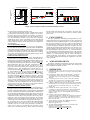
SoC Block Diagram
Core PSM Library
SoC PSM Network
SoC PSM BDD
Core PSM BDDs
Core Power
Equations Library
Monitor File
Symbolic Simulation
Constraints File
Power Computation
+
Power Report
Figure 2: SPA tool flow
PowerPC 405 CPU
DMA
Controller
PLB−OPB Bridge
PLB Bus
Report Power (BDD soc psm states) {
BDD cs = soc psm states; // current states BDD
if (BDD 0(cs) ∨ BDD 1(cs)) return {0, 0};
if (!BDD 0(BDD THEN(cs))) then {
{MinT , MaxT } = Report Power(BDD THEN(cs));
core power = get core psm power(cs);
{Min, Max} = {MinT + core power,
MaxT + core power}; }
{MinE , MaxE } = Report Power(BDD ELSE(cs));
{Min, Max} = {min(Min, MinE ), max(Max, MaxE )};
return {Min, Max}; }
3.2 Power Equations
As mentioned in Section 1, most approaches for early power estimation of chips (prior to the availability of a simulatable functional
description) rely on generalized power equations, adapted from the
2 .f
usual AC power formula: PAC = ∑i Ci .Ai .Vdd
i
i
where Ci is the total capacitance of net i, Ai is the activity factor of
net i (also known as 2 ∗ Switching Factor), Vddi is the power supply for the driver gate of net i, and f i is the clock frequency for the
domain of net i.
This generic equation can be very inaccurate if applied blindly,
but its results can improve significantly if the components in the
chip can be broken down into pieces with similar characteristics
and a tuned power equation applied to each component, with its
own values for capacitance, activity factor, power supply and frequency. The main components of chip power in an SoC which
require a specific power equation (and parameters) are [7]: (1)
Core power, including logic and registers, (2) Clock Tree power, (3)
RAM/ROM read/write power, (4) IO drivers power and (5) Leakage power.
In order to evaluate the formulas for these components, several
estimated parameters need to be provided, such as: capacitance
per unit area, area units per logic gate, clock and data capacitances
per latch, total number of gates and registers per core, switching
activity factors for all components. These parameters depend on the
technology, the cores used in the design, the expected application
(will affect the switching activity), and on power reduction methods
such as clock gating.
3.3 Tool Flow
The algorithms described in this paper have been implemented in
a tool called SPA (for SoC Power Analysis) illustrated in Figure 2.
SPA is used for early power analysis, usually prior to the existence of any executable model (e.g., C, VHDL, Verilog). Hence, the
entry point in the SPA environment is the SoC block diagram, containing the main cores in the SoC, their main interfaces (e.g., master, slave, external bus, etc.), and their power models (e.g., class1, class-2). The designer then manually describes the interconnections among the cores power models by specifying which core
1 For
simplicity, this description assumes no complemented edges.
BDD variable, the core PSM state and its power value can all
be hashed for quick retrieval.
2 The
UART
PLB Arbiter
OPB Bus
EBC
(Ext. Bus Controller)
MC
(Mem. Controller)
EBC_IO
MC_IO
MAL
EMAC
EMAC_IO
Figure 3: Partial PowerPC 405GP design used for state-based
power analysis
PSMs share the same Active or Sleep signal, and how the PSMs
outputs are connected. This can be done using any schematic editor or netlist language. Once the PSM interconnections are defined,
the algorithms described in Sections 2 and 3 generate the BDD representation for the SoC PSM. The symbolic simulation and power
computation step is driven by a Monitor file which specifies the
initial state and the input vectors driving the symbolic simulation.
The user also specifies a State Constraints file which describes the
invalid states in a simple table-like notation.
The power equations and technology parameters for each type
of component are stored in a library and evaluated prior to each
symbolic simulation run. A different equation and parameters can
be associated with each state in each core. The user can change the
parameters and run simulations for several scenarios using script
commands (e.g., Tcl).
4. EXPERIMENTAL RESULTS
To validate the approach we ran the SPA tool on a large portion
of a real design, IBM’s PowerPC 405GP design [8]. The PowerPC
405GP is a system-on-chip containing multiple cores. The example
presented here contains a subset of the cores in the 405GP design,
namely: 405 CPU, PLB Arbiter, Memory controller (MC), DMA
controller, external bus controller (EBC), PLB-OPB bridge, ethernet controller (EMAC), memory access layer (MAL), UART, and
IOs. Each core was mapped to its own PSM, with the addition of
separate IO PSMs for the EMAC, EBC, MC and OTHER IOS (this
is a separate PSM to account for the power in all other chip IOs that
cannot be accounted for under EMAC, EBC and MC IOs). Separate IO PSMs were used for these cores since they are very active
IOs which can be better modeled using their own power formulas.
Without loss of generality, most cores were modeled as class-1, except for the IO PSMs which were modeled as class-0. Figure 3
shows the block diagram of the partial design analyzed for power.
As shown in Figure 1(a) a class-0 PSM has one input called Active, and a class-1 PSM has two inputs called Active and Sleep. The
SoC PSM for the design in Figure 3 has inputs corresponding to the
core PSM inputs, with some inputs being shared. The set of inputs
to the SoC PSM includes: CPU Active, CPU Sleep, DMA active,
MC Active (shared by the Memory controller PSM and its IO
PSM), PLB Active (shared by the PLB Arbiter and the Bridge
PSMs), EMAC Active, EMAC Sleep, MAL Active, MAL Sleep,
among others.
The monitor file contains input vectors for all these input signals.
They can assume values 0, 1 and 2 (for don’t care). For each set
of inputs, the next set of reachable states is derived using symbolic
simulation which iterates until the next set of reachable states is
stable, and its min/max power calculated. The number of iteration
meta-cycles required to reach a stable set of next state is not relevant
Min / Max Average Power
(mW)
1700
a) Power Reachability Analysis
1500
1300
1100
900
b) Power Analysis for EMAC-MAL Packet Receive
1700
1700
1500
1500
1300
1300
1100
1100
900
900
700
700
700
simulation meta-cycles
simulation meta-cycles
simulation meta-cycles
500
500
500
1
2
3
c) Power Analysis for EBC-PLB-DMA-MC Transfer
1
2
3
4
5
6
7
8
9
1
2
3
4
5
6
7
Figure 4: Power analysis for different symbolic simulation scenarios
for the purposes of measuring min/max power.
The constraints file describes the sets of invalid states, used for
pruning the state space during symbolic simulation. In the example above, there were five constraints, for example: (1) if DMA is
active then either the PLB Arbiter or the CPU should also be active; (2) if the Memory controller is Active then its IO component
should also be Active; and (3) if the Bridge is Active then the PLB
Arbiter should also be Active. These constraints can be specified in
a simple table-like notation. Three experiments were conducted as
described below.
a) Power Reachability Analysis
This experiment produces a quick view of the power dissipated by
the SoC under all reachable states. Figure 4(a) shows the Min/Max
power graph for these simulations. The initial state of the symbolic
simulation corresponds to the all Idle state. The second simulation
cycle shows the min/max power for all reachable state, excluding
Sleep states, and the third cycle shows the min/max power for all
reachable states (includind Sleep states).
b) Ethernet Packet Receive Process
This experiment analyzes the min/max power dissipated during a
specific scenario of a packet being received by the Ethernet controller (EMAC) and transmitted to the MAL and onto Memory over
the PLB using the Memory controller (MC). The components that
are activated in turn during the simulation are: EMAC, EMAC IO,
MAL, PLB Arbiter, MC, CPU. The other components are left as
don’t cares, which means that they may stay idle or go to sleep.
Figure 4(b) shows the min/max power reported by the symbolic
simulation process. The simulation starts at the all idle state. It
first activates the EMAC IO and EMAC to receive a packet (cycle
2). Then the MAL becomes active and the EMAC IO may go to
idle (cycle 3). In cycle 4, the MAL transfers the data to memory,
thus activating the PLB arbiter and the Memory controller; while
the EMAC and EMAC IO may transition to idle state. The other
cycles refer to similar transactions between the EMAC, MAL, PLB
and Memory. Of special interest is cycle 7 where the CPU become
Active to process a packet descriptor, which causes a jump in power
dissipation. The line connecting the dots inside each min/max bar
correspond to the power dissipation for the cores involved in the
packet receive process only. This allows us to see where within the
min/max power is the power for a specific scenario.
c) Memory to Memory Transfer Process
This experiment analyzes the min/max power dissipated during a
memory to memory transfer using the external bus controller (EBC),
possibly controlling a Flash memory, transfering data to the SDRAM
memory controlled by the Memory controller (MC). The data transfer uses the PLB and the DMA controller. The CPU is not involved
except for the initial programming of the DMA controller. All other
components are left as don’t cares, possibly in idle or Sleep states.
Figure 4(c) shows the min/max power reported by the symbolic
simulation process. The simulation starts at the all idle state. It first
activates the CPU and the DMA for programming the transfer (cycle 2). Then the CPU is sent to Sleep and the EBC and PLB initiate
the transfer (thus in Active state) in cycle 3. In cycle 4, the DMA
controller is also Active and in cycle 5 the Memory Controller becomes Active as well. In cycle 6 the EBC may go to Idle or Sleep
and in cycle 7 the DMA may also go to Idle. The line connecting
the dots inside each min/max bar correspond to the power dissipation for the cores involved in the memory to memory transfer
process only.
5. CONCLUSIONS
This paper presented a methodology and algorithms for statebased power analysis of core-based systems-on-chip. The approach
combines the use of spreadsheet models (i.e., power equations) and
the power state machine for each core with a formal framework
for computing the product power state machine for the SoC. Then
by means of symbolic simulation techniques, the power states are
visited and the minimum and maximum power for the states computed by adding up the power values for each core in a given state.
The key advantages of this approach are: (a) a formal framework
for computing the maximum and minimum power of all reachable
states, (b) the ability to explore quickly the impact of different parameters, e.g. switching activity, Vdd, etc., and (c) the ability to
explore the dynamic power behavior as time progresses. Results
for a realistic example demonstrated the capabilities of the techniques presented.
6. ACKNOWLEDGMENTS
The authors would like to thank Geert Janssen for help with the
BDD package and Youngsoo Shin and Indira Nair for help with
power simulation of specific scenarios.
7. REFERENCES
[1] R. Bergamaschi and J. Cohn, “The A to Z of SoCs,” in Proceedings of
the IEEE International Conference on Computer-Aided Design, IEEE,
November 2002.
[2] D. Lidsky and J. Rabaey, “Early power exploration - a world wide
web application,” in Proceedings of the 33rd ACM/IEEE Design
Automation Conference, (Las Vegas, NV), pp. 27–32, ACM/IEEE,
June 1996.
[3] S. Gary, P. Ippolito, G. Gerosa, C. Dietz, J. Eno, and H. Sanchez,
“PowerPC 603, a microprocessor for portable computers,” IEEE
Design & Test of Computers, pp. 14–23, Winter 1994.
[4] L. Benini, R. Hodgson, and P. Siege, “System-level power estimation
and optimization,” in Proceedings of the International Symposium on
Low Power Electronics and Design (ISLPD), pp. 173–178, ACM,
August 1998.
[5] F. Balarin, M. Chiodo, P. Giusto, H. Hsieh, J. A, L. Lavagno,
C. Passerone, A. Sangiovanni-Vincentelli, E. Sentovich, K. Suzuki,
and B. Tabbara, Hardware-Software Co-Design of Embedded
Systems: The Polis Approach. The Netherlands: Kluwer Academic
Publishers, 1997.
[6] H. Touati, H. Savoj, B. Lin, R. Brayton, and
A. Sangiovanni-Vincentelli, “Implicit state enumeration of finite state
machines using BDD’s,” in Proceedings of the IEEE International
Conference on Computer-Aided Design, (Santa Clara), pp. 130–133,
IEEE, November 1990.
[7] “Power estimation in ASICs,” 2001. IBM Microelectronics
Application Note. Restricted access through
http://www.edge.ibm.com.
[8] “PowerPC 405GP Embedded Processor User’s Manual,” 2001.
Available for download from
http://www-3.ibm.com/chips/techlib/techlib.nsf/
/products/PowerPC 405GP Embedded Processor.