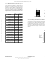
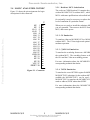
1
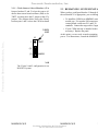
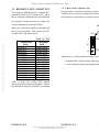
Freescale Semiconductor, Inc.
TABLE OF FIGURES
F i g u r e . . . . . . . . . . . . . . . . . . . . . . . . . . . . . . . . . . . . . . . . . . . . . . . . . . . . . . . . . . . . . . . . . . . . . . . . . . . . . . . . . . . . . . . . . . . . . . . . . . Page
FIGURE 1-1. HC05C9 EMULATOR MODULE..............................................................................1-3
FIGURE 1-2. CONNECTORS P4 AND P5 PIN ASSIGNMENTS......................................................1-4
FIGURE 3-1. CONNECTOR P1 PIN ASSIGNMENTS....................................................................3-10
Freescale Semiconductor, Inc...
M68EM
EMULATOR
TABLE OF TABLES
T a b l e . . . . . . . . . . . . . . . . . . . . . . . . . . . . . . . . . . . . . . . . . . . . . . . . . . . . . . . . . . . . . . . . . . . . . . . . . . . . . . . . . . . . . . . . . . . . . . . . . . . Page USER'S M
TABLE 2-1.
TABLE 2-2.
TABLE 3-1.
TABLE 3-2.
TABLE 3-3.
MCUS EMULATION SELECTION.............................................................................2-4
MCUS AND PERSONALITY FILES...........................................................................2-6
MCUS EMULATION SELECTION.............................................................................3-4
RESIDENT MCUS....................................................................................................3-6
LOGIC ANALYZER CONNECTOR P1 SIGNAL DESCRIPTIONS.................................3-11
Third Ed
© MOTOROLA Ltd., 1994, 199
M68EM05C9/D
iv
For More Information On This Product,
Go to: www.freescale.com
MOTOROLA
Freescale Semiconductor, Inc.
TABLE OF C
Heading................................................
CHAPTER 1 INTRODUCTION . . . . . . . . . . . . . . . . . . . .
Freescale Semiconductor, Inc...
1.1 DEVELOPMENT SYSTEMS.............................
1.1.1
Motorola
Modular
Development
System (MM
Motorola reserves the right to make changes without further notice
to any
products
herein
to
1.1.2 M68HC05EVS Evaluation System (HC05EVS
improve reliability, function, or design. Motorola does not assume
liability arising out of
1.2 any
EM LAYOUT...................................................
the application or use of any product or circuit described herein;
does it convey
1.3 neither
CONNECTORS
P4 ANDany
P5 PIN ASSIGNMENT
1.5
COP
WATCHDOG
EMULATION
CONSIDERAT
license under its patent rights nor the rights of others. Motorola products are not designed,
intended, or authorized for use as components in systems intended
for surgical
implant
into
CHAPTER
2 MMDS05
CONFIGURATION
AND
the body, or other application in which the failure of the Motorola
productC9EM
couldJUMPER
create aHEADERS...............
2.1 SETTING
situation where personal injury or death may occur. Should Buyer2.1.1
purchase
or use Select
Motorola
Clock Source
Headers (J2 and J3).......
2.1.2
Reset
Select
Header
(J4)..............................
products for any such unintended or unauthorized application, Buyer shall indemnify and
2.1.3
Emulation
Device
Selection
(J1, S1).............
hold Motorola and its officers, employees, subsidiaries, affiliates,2.1.4
and Port
distributors
harmless
B Keyboard Interrupt Mask option (S2).
against all claims, costs, damages, and expenses, and reasonable
fees arisingMCU....................................
out of,
2.2attorney
THE EMULATED
directly or indirectly, any claim of personal injury or death associated
2.2.1 with
Resident
such
MCU
unintended
Substitution.........................
2.2.2negligent
C9 Emulation.............................................
or unauthorized use, even if such claim alleges that Motorola was
regarding the
2.2.3 (7)05C4A Emulation...................................
design or manufacture of the part.
2.2.4 705C8 Emulation........................................
2.2.5 705C8A Emulation......................................
Motorola and the Motorola logo are registered trademarks of Motorola Inc. 2.2.6 (7)05C9A Emulation...................................
2.2.7 C12A Emulation.........................................
2.2.8 C2, C3, C4(A), C8, C8(A), C12A Emulation.
Motorola Inc. is an Equal Opportunity/Affirmative Action Employer.
2.3 REMAINING SYSTEM INSTALLATION...........
CHAPTER 3 HC05EVS CONFIGURATION A
3.1 SETTING C9EM JUMPER HEADERS...............
3.1.1 Clock Source Select Headers (J2 and J3).......
3.1.2 Reset Select Header (J4)..............................
3.1.3 Emulation Device Selection (J1, S1).............
3.1.4 Port B Keyboard Interrupt Mask option (S2).
3.2 RESIDENT MCU SUBSTITUTION....................
3.2.1 Resident MCU Substitution.........................
3.2.2 C9 Emulation.............................................
3.2.3 (7)05C4A Emulation...................................
3.2.4 705C8 Emulation........................................
3.2.5 705C8A Emulation......................................
3.2.6 (7)05C9A Emulation...................................
3.2.7 C12A Emulation.........................................
3.2.8 C2, C3, C4(A), C8, C8(A), C12A Emulation..
3.3 EVS LIMITATIONS..........................................
3.4 LOGIC ANALYZER CONNECTOR P1...............
3.5 REMAINING SYSTEM INSTALLATION...........
M68EM05C9/D
For More Information On This Product,
Go to: www.freescale.com
Freescale Semiconductor, Inc.
1.3 CONNECTORS P4 AND P5 PIN ASSIGNMENTS
Figure 1-2 shows the pin assignments for connectors P4 and P5. The signal names used
correspond with the signal names of the MCU. For signal descriptions, consult the technical
data book for the specific MCU.
Freescale Semiconductor, Inc...
1
3
5
7
9
11
13
15
17
19
21
23
25
27
29
31
33
35
37
39
INTRODU
This user's manual explains connection, configu
the M68EM05C9 Emulator Module (C9EM).
debuggingP5
of target systems based on these micro
P4
GND
NC
PA7
PA3
RESET*
Vdd Detect
PD7
PD3
NC
GND
NC
NC
PC0
PC2
PC4
PC6
PB4
PB0
NC
NC
CHAPT
2
4
6
8
10
12
14
16
18
20
22
24
26
28
30
32
34
36
38
40
NC
GND
PA6
PA2
IRQ*
NC
TCMP/PD6
PD2
NC
NC
NC
GND
PC1
PC3
PC5
PC7
PB5
PB1
GND
GND
NC
NC
PA5
PA1
GND
OSC1
TCAP
PD5
PD1
NC
NC
NC
NC
GND
NC
NC
PB6
PB2
NC
NC
MC68HC705C4A
1 MC68HC05C4A
2
NC
3
4
NC MC68HC705C9A
MC68HC05C9A
5
6
PA4
7
8
PA0
The C9EM also emulates
the following parts that
9
10
NC
11 MC68HC05C2
12
NC MC68HC05C3
13
14
GND
15 MC68HC05C8
16
PD4 MC68HC705C8
17
18
PD0
The
of two development sys
19C9EM can be
20partNC
and
layout NC
of the C9EM.
21explains the 22
23
24
NC
25
26
NC
27
28
NC
1.1 DEVELOPMENT
SYSTEMS
29
30
NC
Your
be part
of two Motorola devel
31 C9EM can32
GND
Development
System
or the M68HC
33
34 (MMDS05)
PB7
35
36
PB3
37
38
GND
39
40
1.1.1 Motorola Modular
GND Development Sy
The MMDS05 is an emulator system that pr
memory windows. The unit's integrated design e
Figure 1-2. Connectors P4 and P5 Pin Assignments
user interface, and source-level debug. A comple
As connector P1 has more importance to an HC05EVS than to an MMDS05, pin assignments
• a station module — the metal MMDS05
for connector P1 are in Chapter 3.
the internal power supply. Most system ca
(The cable to an optional target system, ho
To configure your C9EM for use as part of an MMDS05, follow the module
instructions
of Chapter
enclosure
to connect directly to the
2. To configure your C9EM for use as part of an HC05EVS, follow the instructions of
• an emulator module (EM) — such as
Chapter 3.
system functionality for a specific set of
through a sliding panel in the enclosure
cable.
1.5 COP WATCHDOG EMULATION CONSIDERATIONS
• two logic clip cable assemblies —
module to See
yoursections
target system, a test fixtu
Some of the devices emulated by this system include on-chip COP watchdogs.
evaluation
or
analysis.
One end of each ca
2.2.x and 3.2.x for further configuration details.
fits into station-module pod A or pod B. L
in female probe tips. Ball clips come with
M68EM05C9/D
1-4
M68EM05C9/D
MOTOROLA
For More Information On This Product,
Go to: www.freescale.com
1
Freescale Semiconductor, Inc.
• a 9-lead RS-232 serial cable — the cable that connects the station module to the
host computer RS-232 port.
1.2 EM LAYOUT
Freescale Semiconductor, Inc...
• a 9- to 25-pin adapter — a moulded assembly that lets you connect the 9-lead cable
Figure 1-1 shows the layout of the C9EM. Jum
to a 25-pin serial port.
CxA emulation (e.g. C4 vs C4A, C12A). Jump
• system software — software, on 3-1/2 inch diskettes. clock source. Jumper J4 determines the logic
Switch array S1and
determines which dev
• MMDS05 documentation — an MMDS05 operations connector.
manual (MMDS05OM/D)
the user to set the port B mask option for CxA de
the appropriate EM user's manual.
As mentioned, your C9EM gives the MMDS05 the ability to emulate
several
Connectors
P4 MC68HC05Cand P5 provide the interface to th
series MCUs. By substituting a different EM, you can enable the
yourMMDS05
MMDS05station
to emulate
an the target cable p
module,
MCU of a different series. (Your Motorola representative can explain
all the
EMs available.)
enclosure.
Connector
P1 connects to a logic ana
for an EVS system, as an MMDS05 system in
Chapter 2 explains how to configure and use your C9EM as connectors
part of an MMDS05
P2 and P3system.
connect together the EM
For information about MMDS05 software or the station the
module,
see
the
MMDS05
EM and the platform board (for an EVS).
operations manual. For layout and configuration information pertaining to a different EM,
see the corresponding EM user's manual.
1.1.2 M68HC05EVS Evaluation System (HC05EVS)
J1
An HC05EVS is an economical, two-board tool for designing, debugging, and evaluating target
1
systems based on an MC68HC05 MCU. A complete HC05EVS consists of:
• a platform board (PFB) — the bottom board, which supports the emulator module.
The platform board has connectors for power and for the terminal or host computer.
1
1
S1
S2
• an emulator module (EM) — such as the C9EM: a printed circuit board that enables
system functionality for a specific set of MCUs. The EM fits onto the PFB. The EM has
connectors for a target cable and for a cable to a logic analyzer.
• an RS-232 serial cable — the cable that connects the PFB to the host computer RSP2
P1
232 port.
• system software — software, on 3-1/2 inch diskettes.
• HC05EVS documentation — an HC05EVS operations manual (HC05EVSOM/D)
and the appropriate EM user's manual.
J2
1 1
J3
As mentioned, your HC05C9 EVS emulates several MC68HC05C-series MCUs. By
substituting a different EM, you can enable your HC05EVS to emulate an MCU of a different
series. (Your Motorola representative can explain all the EMs available.)
Chapter 3 explains how to configure and use your C9EM as part of an HC05EVS system.
For information about HC05EVS software or the platform board, see the HC05EVS
operations manual. For layout and configuration information pertaining to a different EM,
see the corresponding EM user's manual.
MC68HC05C9
Figure 1-1. HC05C9
M68EM05C9/D
1-2
M68EM05C9/D
MOTOROLA
For More Information On This Product,
Go to: www.freescale.com
1
Freescale Semiconductor, Inc.
2.1.3 Emulation Device Selection (J1, S1)
CHAPT
Switch array S1 and jumper J1 together allow the user to determine the device which is to be
MMDS05
CONFIGURATI
emulated. S1 is used to select the size of the memory map available to the
MCU and also
some device specific features. J1 determines whether the keyboard interrupt function is active
for the CA style devices. The following table shows the settings of S1 and J1 which are
required for each MCU emulated. Section 2.2 discusses the MMDS05
This chapter
personality
explains
fileshow
to be
to configure and us
used with each device and the operation of replacing the resident
other parts
MCU
of system
where installation
this is
or configura
necessary. Note that devices in italics have been or will (MMDS05OM/D).
soon be replaced and
(If you
arewill use your C9E
present for historical reasons only.
Chapter 3 for corresponding information.)
Freescale Semiconductor, Inc...
Paragraph 2.1 explains how to set C9EM
Table 2-1. MCUs Emulation Selection
considerations pertaining to the MCU you emula
installation.
DEVICE
S1 SWITCH S1 SWITCH S1 SWITCH S1 SWITCH
J1 SETTING
M68HC05C2
CLOSED
CLOSED
Note that you can configure a C9EM already
3
4
CA off station-modul
enclosure.
To doC/D
so, switch
of thisON
chapter.
CLOSEDguidance
OPEN
M68HC05C3
CLOSED
CLOSED
CLOSED
OPEN ON
M68HC05C4
CLOSED
CLOSED
CLOSED
OPEN ON
M68HC805C4
CLOSED
CLOSED
CLOSED
M68HC05C8
CLOSED
CLOSED
CLOSED
Be sure ON
to switch off power if you reconf
OPEN
EM jumper headers with power left on can
OPEN ON
M68HC705C8
OPEN
CLOSED
CLOSED
OPEN ON
M68HC05C9
CLOSED
OPEN
CLOSED
OPEN ON
M68HC705C9
CLOSED
OPEN
M68HC05C4A
CLOSED
CLOSED
CLOSEDYour C9EM
OPENhas
ON
four jumper headers, J1 throu
2.1.1. throughON
2.1.4 explain how to co
CLOSEDParagraphs
OPEN
M68HC705C4A
CLOSED
CLOSED
CLOSED
OPEN
ON
M68HC05C8A
CLOSED
CLOSED
CLOSED
OPEN
ON
M68HC705C8A
OPEN
CLOSED
CLOSED
OPEN
ON
M68HC05C9A
CLOSED
OPEN
CLOSED
OPEN
ON
M68HC705C9A
CLOSED
OPEN
CLOSED
OPEN
ON
M68HC05C12A
CLOSED
OPEN
CLOSED
OPEN
ON
1
M68EM05C9/D
2
2-4
CAUTI
2.1 SETTING C9EM JUMPER HEA
M68EM05C9/D
MOTOROLA
For More Information On This Product,
Go to: www.freescale.com
2
Freescale Semiconductor, Inc.
2.1.1 Clock Source Select Headers (J2 and J3)
2.1.2 Reset Select Header (J4)
Jumper headers J2 and J3 select the source of the clock oscillator
Jumper
for header
the MCU.
J4 controls
You may
the path of a target r
choose between on-board oscillator (EM), MMDS supplied configuration:
oscillator (MMDS)
the fabricated
or clockjumper between p
from the target system (TRGT). To select MMDS you must place
resets.theThis
J3 jumper
is the only
at thecorrect
(J2) J4 configuration
position as well as correctly selecting the J2 setting. The diagram below shows the factory
configuration: the fabricated jumper on J3 between pins 1 and 2 selects the C9EM on-board
canned oscillator clock source.
FA
Freescale Semiconductor, Inc...
FABRICATED
JUMPERS
J2
1
1
J3
TRGT
1
(2)
(3)
J4
XTAL
(2)
MMDS
(3)
EVS
(2)
(3)
TRG
(J2)
NOT
Alternatively, you may use a clock source originating from the control
board.
To do so,
The J2
pins 2-and-3
configuration is not
position the J3 jumper between pins 2 and 3, then use the MMDS05 OSC
command
to select
MMDS05
system.
Such a configuration w
a frequency. To use a clock source originating from the target system of
position
the J3 jumper
the RESETIN
and RESETOUT comma
between pins 2 and 3, then position the J2 jumper between pins 1 and 2.
M68EM05C9/D
2-2
M68EM05C9/D
MOTOROLA
For More Information On This Product,
Go to: www.freescale.com
2
Freescale Semiconductor, Inc.
2.2.5 705C8A Emulation
To emulate the exact OPTION register RAM/ROM behaviour, and watchdog function of an
MC68HC705C8A, use a MC68HC705C8A substitute for the resident MCU. By restricting
S1used
the use of the RAM/ROM available, and watchdog function the MC68HC705C9 can be
as the resident MCU. When using the MC68HC705C9 to emulate the MC68HC705C8A
1
writes to the OPTION register should be made to address $3FDF rather than $1FDF.
2
For more information about the MC68HC705C8A and MC68HC705C9 features,3 see the
corresponding technical data books.
4
Open
1
(2)
(3
Closed
Freescale Semiconductor, Inc...
2.2.6 (7)05C9A Emulation
To emulate an MC68HC(7)05C9A, use the MC68HC705C9 for the resident MCU.
2.1.4 Port B Keyboard Interrupt Mask o
For more information about the MC68HC05C9A and MC68HC705C9
see
the bits in port B hav
Switch arrayfeatures,
S2 selects
which
corresponding technical data books.
CxA type devices. (The switch S2 settings sho
that you require for the device; in the 705C8A
selected are only active when programmed as in
2.2.7 C12A Emulation
in such cases a resistive pull up is activated on th
for MC68HC05C12A
the keyboard interrupt
bit close the relevan
To emulate the watchdog feature on a MC68HC05C12A use the
for the
selects
the
CA
option.
Switch
resident MCU. The watchdog feature on the MC68HC705C9 is different from that on the array S2 is organis
C12A.
For more information about the MC68HC05C12A and MC68HC705C9 features, see the
corresponding technical data books.
2.2.8 C2, C3, C4(A), C8, C8(A), C12A Emulation
Port B
To emulate an MC68HC05C2,C3,C4(A),C8, you may use the MC68HC705C9 for the bits
resident MCU. Remember that these devices do not include all the MC68HC705C9 features. selected
For accurate emulation, do not use any of the additional MC68HC705C9 features.
For example, the MC68HC705C9 has an OPTION register at address $3FDF. This register
can enable extra RAM and ROM in memory, be careful therefore not to disturb bit 6 and 7 of
this register when emulated one of the above devices. This OPTION register also includes a
bit which deteremines IRQ sensitivity; either edge only or level and edge. This bit (1) may be
used to emulate the IRQ mask option on these devices.
S2
0
1
2
3
4
5
6
7
Open
For more information about the MC68HC05C2, C3, C4(A), C8(A) and MC68HC705C9
features, see the corresponding technical data books.
M68EM05C9/D
2-8
M68EM05C9/D
MOTOROLA
For More Information On This Product,
Go to: www.freescale.com
2
Freescale Semiconductor, Inc.
2.2.1 Resident MCU Substitution
2.2 THE EMULATED MCU
socket
C9EM
location U9 contains the r
Your MMDS05 system uses a specific personality file for theThe
MCU
typeatbeing
emulated.
with MCU,
an MC68HC705C9
resident MCU, which
For example, to emulate an MC68HC05C9 or MC68HC705C9
the system uses
MCUs
with
some
qualifications
personality file 0021AVxx.MEM. Table 2-1 lists all the personality files that pertain to the as described in th
C9EM. Note that personality file names follow the pattern Occasionally
00ZZZVxx.MEM,
it may be where
necessary to replace the
ZZZ is the EM identifier or MCU name, and xx is the version of
the of
file.
Note that
level
emulation
of adevices
particular feature.
in italics have been or will soon be replaced and are present for historical reasons
only.
When you are ready to install the substitute MC
that you are grounded. Then remove the MCU
Table 2-2. MCUs and Personalityresident
Files MCU, and restore power.
Freescale Semiconductor, Inc...
EMULATED
MCU
M68HC05C2
M68HC05C3
M68HC05C4
M68HC805C4
M68HC05C8
M68HC705C8
M68HC05C9
M68HC705C9
M68HC05C4A
M68HC705C4A
M68HC05C8A
M68HC705C8A
M68HC05C9A
M68HC705C9A
M68HC05C12A
PERSONALITY
FILE
00C2_V01.MEM
00C3_V01.MEM
00C4_V01.MEM
00C4_V01.MEM
00218V01.MEM
00219V01.MEM
0021AV01.MEM
0021AV01.MEM
00C4AV01.MEM
00C4AV01.MEM
00218V01.MEM
00219V01.MEM
0021AV01.MEM
0021AV01.MEM
00C12V01.MEM
COMMENTS
2.2.2 C9 Emulation
See paragraphs 2.2.1 and 2.2.8.
To2.2.1
emulate
See paragraphs
and either
2.2.8. an MC68HC05C9 or MC68
resident
MCU.
The C9 has single mask option f
See paragraphs
2.2.1 and
2.2.8.
See paragraphs
emulator
2.2.1 and
operation.
2.2.8.
See paragraphs 2.2.1 and 2.2.8.
See paragraph 2.2.1, 2.2.4 and 2.2.8
See paragraph2.2.3
2.2.2.(7)05C4A Emulation
See paragraph 2.2.2.
emulate
theand
watchdog
See paragraphsTo
2.2.1,
2.2.3
2.2.8. feature on a MC68HC
See paragraphsthe
2.2.1,
resident
2.2.3MCU.
and 2.2.8.
The watchdog feature on th
See paragraphthe
2.2.1
and
2.2.8.
C4A and the C4 has no watchdog present.
See paragraph 2.2.1, 2.2.5 and 2.2.8.
See paragraphFor
2.2.1
andinformation
2.2.6.
more
about the MC68HC05C
See paragraphcorresponding
2.2.1 and 2.2.6.
technical data books.
See paragraphs 2.2.1, 2.2.7 and 2.2.8.
MMDS05 software loads the personality file upon powerup. To replace the default
2.2.4 (For
705C8
Emulation
personality file with a different one, use the LOADMEM command.
more
information
about the LOADMEM command, see the explanation in the MMDS05
operations
manual.)
To emulate
the exact
OPTION register RAM/R
MC68HC705C8 substitute for the resident MCU
Alternatively, you can insert the line LOADMEM 00ZZZVxx.MEM
theMC68HC705C9
STARTUP.05 can be used a
available inthe
script file. This way, the system automatically loads the specified
personality file
as part of
MC68HC05C9
to emulate
the MC68HC705C8
system startup. (For more information about the STARTUP.05
script
file,
see
the
SCRIPT
made to address $3FDF rather than $1FDF.
command explanation in the MMDS05 operations manual.)
For more information about the MC68HC705
corresponding technical data books.
M68EM05C9/D
2-6
M68EM05C9/D
MOTOROLA
For More Information On This Product,
Go to: www.freescale.com
2
Freescale Semiconductor, Inc.
3.1.1 Clock Source Select Headers (J2 and J3)
2.3 REMAINING SYSTEM INSTA
Jumper headers J2 and J3 select the source of the clock oscillator
thehave
MCU.
You may
Whenfor
you
configured
headers J1 through J4
choose between on-board oscillator (EM) or clock from the target
select you are through
the system
resident(TOSC).
MCU is To
appropriate,
TRGT you must place the J3 jumper at the (J2) position as well as selecting TRGT on the J2
jumper. The diagram below shows the factory configuration: the• fabricated
on in
J3an MMDS05 statio
To install jumper
the C9EM
between pins 1 and 2 selects the C9EM on-board canned oscillator clock
source.
module top. Fit together EM connectors
control-board connectors P11 and P12.
standoffs. Connect the target cable, if appr
FABRICATED
JUMPERS
At this point, you are ready to make remaining
J3 power. For instructions, consult the MMDS05 o
Freescale Semiconductor, Inc...
J2
1
TRGT
1
(2)
(3)
• If your C9EM already is installed in the s
necessary). Replace the panel.
XTAL
(2)
MMDS
(3)
(J2)
NOTE
The J2 pins 2-and-3 configuration is not correct for a C9EM that is part of an
HC05EVS system.
M68EM05C9/D
3-2
M68EM05C9/D
MOTOROLA
For More Information On This Product,
Go to: www.freescale.com
2
Freescale Semiconductor, Inc.
CHAPT
HC05EVS CONFIGURATI
This chapter explains how to configure your C
other parts of system installation or configura
(HC05EVSOM/D). (If you will use your C9
Chapter 2 for configuration information.)
Paragraph 3.1 explains how to set C9EM
considerations pertaining to the MCU you emul
the C9EM in an HC05EVS. Paragraph 3.4 expl
for the logic analyzer connector (P1). Paragraph
Freescale Semiconductor, Inc...
Note that you can configure a C9EM already ins
do so, disconnect platform-board power, then fol
CAUTI
This page intentionally left blank
Be sure to disconnect power if you reconf
EM jumper headers with power left on can
3.1 SETTING C9EM JUMPER HEA
Your C9EM has four jumper headers, J1 throu
Paragraphs 3.1.1. through 3.1.4 explain how to co
M68EM05C9/D
2-10
M68EM05C9/D
MOTOROLA
For More Information On This Product,
Go to: www.freescale.com
3
Freescale Semiconductor, Inc.
3.1.2 Reset Select Header (J4)
3.2 RESIDENT MCU SUBSTITUTION
header
J4 controls
the path of a target r
The socket at C9EM location U9 contains the resident MCU. Jumper
The factory
ships
the C9EM
with an MC68HC705C9 resident MCU, which is appropriateconfiguration:
for emulatingthe
a fabricated
number ofjumper between pi
target
when
you
press
user or master reset sw
MCUs with some qualifications as described in the following paragraphs 3.2.2 throughthe
3.2.8.
Occasionally it may be necessary to replace the resident MCU with another to improve the
level of emulation of a particular feature.
FA
Freescale Semiconductor, Inc...
When you are ready to install the substitute MCU, turn off MMDS05 power and make sure
that you are grounded. Then remove the MCU from C9EM location U9, insert the new
resident MCU, and restore power.
1
Table 3-2. Resident MCUs
EMULATED
MCU
M68HC05C2
M68HC05C3
M68HC05C4
M68HC805C4
M68HC05C8
M68HC705C8
M68HC05C9
M68HC705C9
M68HC05C4A
M68HC705C4A
M68HC05C8A
M68HC705C8A
M68HC05C9A
M68HC705C9A
M68HC05C12A
RESIDENT
MCU
MC68HC705C9
MC68HC705C9
MC68HC705C9
MC68HC705C9
MC68HC705C9
MC68HC705C9
MC68HC705C9
MC68HC705C9
MC68HC705C9
MC68HC705C9
MC68HC705C9
MC68HC705C9
MC68HC705C9
MC68HC705C9
MC68HC705C9
J4
EVS
COMMENTS
(2)
See paragraphs 3.2.1 and 3.2.8.
See paragraphs 3.2.1 and 3.2.8.
TRG
(3)
See paragraphs 3.2.1 and 3.2.8.
See paragraphs 3.2.1 and 3.2.8.
See paragraphs
3.2.1 and 3.2.8.
Alternatively,
you may enable the target system
See paragraph 3.2.1, 3.2.4 and 3.2.8
See paragraph 3.2.2.
• Reposition the C9EM J4 jumper between p
See paragraph 3.2.2.
• Insert
a fabricated
jumper into platform-boa
See paragraphs 3.2.1,
3.2.3
and 3.2.8.
See paragraphs 3.2.1, 3.2.3 and 3.2.8.
See paragraph 3.2.1 and 3.2.8.
See paragraph 3.2.1, 3.2.5 and 3.2.8.
See paragraph 3.2.1 and 3.2.6.
See paragraph 3.2.1 and 3.2.6.
See paragraphs 3.2.1, 3.2.7 and 3.2.8.
Table 3-1 shows the resident MCU appropriate for your emulation with additional
information in th reference paragraphs. Also note paragraphs 3.2.2 through 3.2.8, below, for
the information specific to the MCU you emulate.
M68EM05C9/D
3-6
M68EM05C9/D
MOTOROLA
For More Information On This Product,
Go to: www.freescale.com
3
Freescale Semiconductor, Inc.
3.1.3 Emulation Device Selection (J1, S1)
Switch array S1 and jumper J1 together allow the user to determine the device which is to be
emulated. S1 is used to select the size of the memory map available to the MCU and also
some device specific features. J1 determines whether the keyboard interrupt function is active
for the CxA style devices. The following table shows the settings of S1 and J1 which are
S1 be
required for each MCU emulated. Note that devices in italics have been or will soon
replaced and are present for historical reasons only.
1
2
Table 3-1. MCUs Emulation Selection
3
4
DEVICE
S1 SWITCH S1 SWITCH S1 SWITCH S1 SWITCH J1 SETTING
Freescale Semiconductor, Inc...
1
2
3
4
1
(2)
(3
C/D
OpenCA Closed
OPEN ON
M68HC05C2
CLOSED
CLOSED
CLOSED
M68HC05C3
CLOSED
CLOSED
M68HC05C4
CLOSED
CLOSED
M68HC805C4
CLOSED
CLOSED
M68HC05C8
CLOSED
CLOSED
M68HC705C8
OPEN
CLOSED
M68HC05C9
CLOSED
OPEN
CLOSED3.1.4 Port
OPENB ON
Keyboard Interrupt Mask o
CLOSEDSwitch OPEN
array S2ON
selects which bits in port B hav
devices.
CLOSEDCxA type
OPEN
ON The bits selected are only ac
port B data direction register, in such cases a
CLOSEDquestion.
OPEN
To enable
ON the mask option for the key
in S2 and ensure that jumper J1 selects the CA
CLOSEDfollows:OPEN ON
CLOSED
OPEN ON
M68HC705C9
CLOSED
OPEN
CLOSED
OPEN ON
M68HC05C4A
CLOSED
CLOSED
CLOSED
OPEN
ON
M68HC705C4A
CLOSED
CLOSED
CLOSED
OPEN
ON
M68HC05C8A
CLOSED
CLOSED
CLOSED
OPEN
ON
M68HC705C8A
OPEN
CLOSED
CLOSED
OPEN
ON
M68HC05C9A
CLOSED
OPEN
CLOSED
OPEN
ON
M68HC705C9A
CLOSED
OPEN
CLOSED
OPEN
ON
M68HC05C12A
CLOSED
OPEN
CLOSED
OPEN
ON
S2
Port B
bits
selected
0
1
2
3
4
5
6
7
Open
M68EM05C9/D
3-4
M68EM05C9/D
MOTOROLA
For More Information On This Product,
Go to: www.freescale.com
3
Freescale Semiconductor, Inc.
3.4 LOGIC ANALYZER CONNECTOR P1
3.2.1 Resident MCU Substitution
The P1.
socket
at C9EM
location
Figure 3-1 shows the pin assignments for logic analyzer connector
Table
3-2 lists
signal U9 contains the r
with an MC68HC705C9 resident MCU, which
descriptions for this connector.
MCUs with some qualifications as described in th
Occasionally it may be necessary to replace the
level of emulation of a particular feature.
P1
Freescale Semiconductor, Inc...
NC
NC
LA11
LA10
LA9
LA8
LA7
LA6
LA5
LA4
LA3
LA2
LA1
LA0
LR/W
NC
NC
NC
VCC
RESET
1
3
5
7
9
11
13
15
17
19
21
23
25
27
29
31
33
35
37
39
2
4
6
8
10
12
14
16
18
20
22
24
26
28
30
32
34
36
38
40
GNDWhen you are ready to install the substitute MC
NC you are grounded. Then remove the MCU from
GNDMCU, and restore power.
LA12
LA13
NC 3.2.2 C9 Emulation
NC
To emulate either an MC68HC05C9 or MC68
D7
resident MCU. The C9 has single mask option f
D6
emulator operation.
D5
D4
D3
D2 3.2.3 (7)05C4A Emulation
D1 To emulate the watchdog feature on a MC68HC
D0 the resident MCU. The watchdog feature on th
LIR the C4A and the C4 has no watchdog present.
NC
NC For more information about the MC68HC05C
E corresponding technical data books.
NC
3.2.4 705C8 Emulation
Figure 3-1. Connector P1 Pin Assignments
To emulate the exact OPTION register RAM/R
MC68HC705C8 substitute for the resident MCU
available the MC68HC705C9 can be used a
MC68HC705C9 to emulate the MC68HC705C
made to address $3FDF rather than $1FDF.
For more information about the MC68HC705
corresponding technical data books.
M68EM05C9/D
3-10
M68EM05C9/D
MOTOROLA
For More Information On This Product,
Go to: www.freescale.com
3
Freescale Semiconductor, Inc.
3.2.5 705C8A Emulation
3.3 EVS LIMITATIONS
To emulate the exact OPTION register RAM/ROM behaviour,This
and watchdog
anlimitations that ap
paragraphfunction
explainsofthe
MC68HC705C8A, use a MC68HC705C8A substitute for the resident
MCU. Byapply
restricting
(These limitations
regardless of the residen
the use of the RAM/ROM available, and watchdog function the MC68HC705C9 can be used
as the resident MCU. When using the MC68HC05C9 to emulate
the MC68HC705C8A
Limitation
1. CLI/RTI. You may not trace a
writes to the OPTION register should be made to address $3FDF
rather
$1FDF.
interruptthan
(RTI)
instruction with an interrupt en
handling. Attempting such a trace causes an i
For more information about the MC68HC705C8A and MC68HC705C9
features,
the
software reset
of thesee
HC05EVS.
User brea
corresponding technical data books.
instructions; you must remove such SWI instruct
Limitation 2. Branch. Do not trace a condition
branches to itself. As the monitor places an SW
never MCU.
would execute the instruction. H
To emulate an MC68HC(7)05C9A, use the MC68HC705C9 forsystem
the resident
instruction had executed. You may enter a G c
instruction asfeatures,
long as the
is not a brea
For more information about the MC68HC05C9A and MC68HC705C9
seeinstruction
the
corresponding technical data books.
Limitation 3. IRQ/SWI. Whenever possible,
user software interrupts (SWIs). This preven
concurrent hardware interrupt and SWI could c
3.2.7 C12A Emulation
program execution. To recover from such a
To emulate the watchdog feature on a MC68HC05C12A use the
MC68HC05C12A
for the reset switch (SW3
statistically),
press the master
resident MCU. The watchdog feature on the MC68HC705C9 is different from that on the
C12A.
Limitation 4. Memory Map. You must be aw
simulated; be sure to use only valid ROM lo
For more information about the MC68HC05C12A and MC68HC705C9
see programs
the
protection tofeatures,
limit user
to the exac
corresponding technical data books.
information about memory maps, consult the tec
Freescale Semiconductor, Inc...
3.2.6 (7)05C9A Emulation
Limitation 5. COP. The computer operating p
3.2.8 C2, C3, C4(A), C8, C8(A), C12A Emulation EPROM location for the resident MCU. Acc
jumper header must enable write protection. O
To emulate an MC68HC05C2,C3,C4(A),C8, you may use the
MC68HC705C9
forstored
the in user pseudo R
register
change the value
resident MCU. Remember that these devices do not include all the MC68HC705C9 features.
For accurate emulation, do not use any of the additional MC68HC705C9 features.
For example, the MC68HC705C9 has an OPTION register at address $3FDF. This register
can enable extra RAM and ROM in memory, be careful therefore not to disturb bit 6 and 7 of
this register when emulated one of the above devices. This OPTION register also includes a
bit which deteremines IRQ sensitivity; either edge only or level and edge. This bit (1) may be
used to emulate the IRQ mask option on these devices.
For more information about the MC68HC05C2, C3, C4(A), C8(A) and MC68HC705C9
features, see the corresponding technical data books.
M68EM05C9/D
3-8
M68EM05C9/D
MOTOROLA
For More Information On This Product,
Go to: www.freescale.com
3
Freescale Semiconductor, Inc.
Table 3-3. Logic Analyzer Conn
3.5 REMAINING SYSTEM INSTALLATION
PIN
When you have configured headers J1 through J4 and switches S1 and
1, S2,
3, and
4, made
10, -sure
- - - - that
the resident MCU is appropriate, you are through with C9EM configuration.
12, 14, 31, 33
No connec
Find jumper header J1 of the HC05EVS platform board. Make
jumpers are installed, per the diagram below.
GROUND
LATCHED A
output add
J1
Freescale Semiconductor, Inc...
MNEMONIC
A14
1
2
A13
3
4
A12
5
6
A11
7
8
— 36, 40
sure
2, 6that three fabricated
GND
5, 7, 8, 9, 11. LA13 — LA0
13. 15. 17,
19, 21, 23,
25, 27
8
LA12
16, 18,
22, 24,
28, 30
29
FABRICATED
JUMPERS
20, AD7 — AD0
26,
LR/W
32
LIR
37
VCC
38
E
To install the C9EM on an HC05EVS platform board, fit together EM connectors P2 and P3
(on the bottom of the board) and platform-board connectors P3 and P4. Snap the corners of
39
RESET
the EM onto the plastic standoffs.
LATCHED
output add
DATA BUS
bus.
LATCHED
signal tha
transferred
LOAD INS
active-low
instruction
+5 VDC PO
used by EV
EXTERNAL
clock sign
frequency
of the sign
RESET starting an
At this point, you are ready to make remaining cable connections, as necessary, and restore
power. For instructions, consult the HC05EVS operations manual (HC05EVSOM/D).
M68EM05C9/D
3-12
M68EM05C9/D
MOTOROLA
For More Information On This Product,
Go to: www.freescale.com
3