1
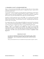
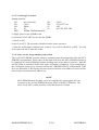
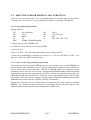
M68HC05PGMR-2/D
Rev 2
April 1995
M68HC05PGMR-2
PROGRAMMER
USER'S MANUAL
Third Edition
© MOTOROLA Ltd., 1994, 1995; All Rights Reserved
M68HC05PGMR-2/D
2-1
MOTOROLA
Motorola reserves the right to make changes without further notice to any products herein to
improve reliability, function, or design. Motorola does not assume any liability arising out of
the application or use of any product or circuit described herein; neither does it convey any
license under its patent rights nor the rights of others. Motorola products are not designed,
intended, or authorized for use as components in systems intended for surgical implant into
the body, or other application in which the failure of the Motorola product could create a
situation where personal injury or death may occur. Should Buyer purchase or use Motorola
products for any such unintended or unauthorized application, Buyer shall indemnify and
hold Motorola and its officers, employees, subsidiaries, affiliates, and distributors harmless
against all claims, costs, damages, and expenses, and reasonable attorney fees arising out of,
directly or indirectly, any claim of personal injury or death associated with such unintended
or unauthorized use, even if such claim alleges that Motorola was negligent regarding the
design or manufacture of the part.
Motorola and the Motorola logo are registered trademarks of Motorola Inc.
Motorola Inc. is an Equal Opportunity/Affirmative Action Employer.
M68HC05PGMR-2/D
2-2
MOTOROLA
Table of Contents
1. INTRODUCTION...................................................................................1-5
1.1 BOARD LAYOUT AND DESCRIPTION...................................................................................1-6
2. PROGRAMMING PROCEDURES . . . . . . . . . . . . . . . . . . . . . . . . . . . . . . . . . . . . . . . . . . . . . . . . . . . . . . . . . . . . . . 2 - 7
2.1 68HC805C4 PROGRAMMING AND VERIFYING....................................................................2-7
2.1.1 Programming Procedure.....................................................................................................2-7
2.1.2 Notes on the Programming Operation...................................................................................2-7
2.1.3 Verifying Procedure...........................................................................................................2-8
2.1.4 Notes on the Programming Operation...................................................................................2-8
2.2 68HC705C5 PROGRAMMING AND VERIFYING....................................................................2-9
2.2.1 Programming Procedure.....................................................................................................2-9
2.2.2 Notes on the Programming Operation...................................................................................2-9
2.2.3 Verifying Procedure.........................................................................................................2-10
2.2.4 Notes on the Programming Operation.................................................................................2-10
2.3 68HC705C8 PROGRAMMING AND VERIFYING..................................................................2-11
2.3.1 Programming Procedure...................................................................................................2-11
2.3.2 Notes on the Programming Operation.................................................................................2-11
2.3.3 Verifying Procedure.........................................................................................................2-12
2.3.4 Notes on the Verifying Operation......................................................................................2-12
2.3.5 Secure EPROM Operation................................................................................................2-13
2.4 68HC705C9/D9 PROGRAMMING AND VERIFYING.............................................................2-14
2.4.1 Programming Procedure...................................................................................................2-14
2.4.2 Notes on the Programming Operation.................................................................................2-14
2.4.3 Verifying Procedure.........................................................................................................2-15
2.4.4 Notes on the Verifying Operation......................................................................................2-15
M68HC05PGMR-2/D
2-3
MOTOROLA
THIS PAGE INTENTIONALLY LEFT BLANK
M68HC05PGMR-2/D
2-4
MOTOROLA
CHAPTER 1.
INTRODUCTION
This manual describes the procedure used to program and verify an MC68HC(7/8)05C series
microcontroller (MCU) on the M68HC05PGMR-2. All that is required to program the
MCU is the PGMR, +5 volt and VPP dc power supply, and a pre-programmed EPROM.
The PGMR provides programming for either 40 pin dual-in-line package (DIP) MCU device
programming, or 44 pin plastic leaded chip carrier (PLCC) MCU device programming.
Install power
leads at P1
S1 controls power
to the MCU
S2 controls the
MCU RESET
Jumper Headers
configure the PGMR
JP3
P1
S1
S2
JP1 JP2
JP5
S3
JP4
P2
SKT2
SKT1
SKT3
SKT1 contains
the program EPROM
Install the 40DIP
MCU in SKT2
OR
Install the 44PLCC
MCU in SKT1
Figure 1.1 M68HC05PGMR-2 Layout
M68HC05PGMR-2/D
2-5
MOTOROLA
1.1 BOARD LAYOUT AND DESCRIPTION
Figure 1.1 shows the layout of the PGMR. As shown in the figure there are various controls,
connectors and sockets that provide the ability to configure the board to specific MCU
programming requirements.
For the board to function correctly you must supply the required power to the board at
connector P1. +5V dc @ 100mA and ground lines are required. In addition a VPP power
supply is needed to perform the programming. The value of this supply may vary between
MCUs, please refer to this manual and the device data book for further information.
Switches S1 and S2 control the activity of the PGMR. S1 is a simple on/off switch that
applies power to the MCU device when on. Never remove or install an MCU when the S1
switch is in the ON position. S2 control the MCU reset line. Programming cannot take place
while the part is in reset mode.
Five jumper headers (JP1 to JP5) configure the PGMR for the particular MCU and function
in use. They select between different MCUs, EPROM sizes, and modes. The following
sections describe how to configure these jumpers for your programming requirements.
Lastly, sockets SKT1 to SKT3 allow for the installation of the MCUs and the master
EPROM. SKT1 is for installation of the EPROM that contains all the data being
programmed into the MCU. SKT2 provides support for a 40 pin DIP package and SKT3 for
a 44 pin PLCC package. Not all of the MCUs supported by this board may be available in
each package. The SKT3 socket requires that the MCU is installed in a top-down or deadbug fashion.
IMPORTANT NOTE
You must never install more than one MCU on this board at any time. That is
there must never be an MCU installed in SKT2 and another installed in SKT3
simultaneously. Such a configuration may damage either of the MCUs and the
board itself.
Always ensure that the devices are orientated correctly into their respective sockets.
M68HC05PGMR-2/D
2-6
MOTOROLA
CHAPTER 2.
PROGRAMMING PROCEDURES
The programmer copies a user program contained in an external EPROM, into the internal
PROM (OTPROM/EPROM) or EEPROM (C4 only) of the MCU device
The following sections describe the procedure taken to program each MCU type.
2.1 68HC805C4 PROGRAMMING AND VERIFYING
There are two procedures used: one for programming and verifying and one that allows
verifying only.
2.1.1 Programming Procedure
Settings required:
JP1
JP3
JP5
S2
SKT1
No Connection
C4/C8
PROG
IN
27C64 EPROM Installed
JP2
JP4
S1
S3
C4/C8
27C64/27C128
OFF
OFF OFF OFF OFF
a) Apply power to the PGMR board.
b) Insert the 805C4 MCU device into the PGMR.
c) Set S1 to ON.
d) Set S2 to OUT. The selected programming routine is then executed.
e) Once the programming is complete (see section 2.1.2), set S2 to IN and S1 to OFF. You
may now remove the MCU from the socket.
2.1.2 Notes on the Programming Operation
In the program and verify MCU PROM routine, the contents of an external EPROM are
copied into the MCU EEPROM. There is a direct correlation of addresses between the two
devices (MCU and external EPROM). Non-MCU EEPROM addresses are ignored so data
contained in those areas are not accessed. Unprogrammed EEPROM address locations should
contain $FF to speed up the programming operation. During the programming routine, the
PROGRAM LED D6 is illuminated. At the end of the programming routine, D6 is turned
off, and the verification routine is entered. If the contents of the MCU EEPROM and
external EPROM exactly match, then the VERIFY LED D5 is illuminated.
M68HC05PGMR-2/D
2-7
MOTOROLA
During the verification routine, all locations are compared to the data residing in external
EPROM. The verification routine will stop if a discrepancy has been detected and the error
address location will be placed on the external memory address bus.
2.1.3 Verifying Procedure
Settings required:
JP1
JP3
JP5
S2
SKT1
No Connection
C4/C8
PROG
IN
27C64 EPROM Installed
JP2
JP4
S1
S3
C4/C8
27C64/27C128
OFF
OFF ON OFF OFF
a) Apply power to the PGMR board.
b) Insert the 805C4 MCU device into the PGMR.
c) Set S1 to ON.
d) Set S2 to OUT. The selected verification routine is then executed.
e) Once the verification is complete (see section 2.1.4), set S2 to IN and S1 to OFF. You may
now remove the MCU from the socket.
2.1.4 Notes on the Programming Operation
The verify MCU EEPROM contents routine is normally entered automatically after the
MCU EEPROM is programmed. Direct entry of this mode will cause the MCU EEPROM
contents to be compared to external EPROM contents residing at the same address locations.
Both D5 and D6 LEDs are turned off at this time until verification is completed. Upon
completion of the verification routine (every location verified) the VERIFIED LED D5 is
illuminated. If D5 does not illuminate, a discrepancy has been detected and the error address
location will be placed on the external memory address bus.
NOTE
MCU EEPROM blank checking can be accomplished by placing $FF into the
locations of the external EPROM that map those of the MCU EEPROM. The
above verify MCU routine will then verify that the device is blank.
M68HC05PGMR-2/D
2-8
MOTOROLA
2.2 68HC705C5 PROGRAMMING AND VERIFYING
There are two procedures used: one for programming and verifying and one that allows
verifying only.
2.2.1 Programming Procedure
Settings required:
JP1
JP3
JP5
S2
SKT1
No Connection
C4/C8
PROG
IN
27C64 EPROM Installed
JP2
JP4
S1
S3
C4/C8
27C64/27C128
OFF
ON OFF OFF OFF
a) Apply power to the PGMR board.
b) Insert the 705C5 MCU device into the PGMR.
c) Set S1 to ON.
d) Set S2 to OUT. The selected programming routine is then executed.
e) Once the programming is complete (see section 2.1.2), set S2 to IN and S1 to OFF. You
may now remove the MCU from the socket.
2.2.2 Notes on the Programming Operation
In the program and verify MCU EPROM routine, the contents of an external EPROM are
copied into the MCU EPROM. There is a direct correlation of addresses between the two
devices (MCU and external EPROM). Non-MCU EPROM addresses are ignored so data
contained in those areas are not accessed. Unprogrammed EPROM address locations should
contain $00 to speed up the programming operation. During the programming routine, the
PROGRAM LED D6 is illuminated. At the end of the programming routine, D6 is turned
off, and the verification routine is entered. If the contents of the MCU EPROM and external
EPROM exactly match, then the VERIFY LED D5 is illuminated.
During the verification routine, all locations are compared to the data residing in external
EPROM. The verification routine will stop if a discrepancy has been detected and the error
address location will be placed on the external memory address bus.
M68HC05PGMR-2/D
2-9
MOTOROLA
2.2.3 Verifying Procedure
Settings required:
JP1
JP3
JP5
S2
SKT1
No Connection
C4/C8
PROG
IN
27C64 EPROM Installed
JP2
JP4
S1
S3
C4/C8
27C64/27C128
OFF
ON ON OFF OFF
a) Apply power to the PGMR board.
b) Insert the 705C5 MCU device into the PGMR.
c) Set S1 to ON.
d) Set S2 to OUT. The selected verification routine is then executed.
e) Once the verification is complete (see section 2.2.4), set S2 to IN and S1 to OFF. You may
now remove the MCU from the socket.
2.2.4 Notes on the Programming Operation
The verify MCU PROM contents routine is normally entered automatically after the MCU
EPROM is programmed. Direct entry of this mode will cause the MCU EPROM contents to
be compared to external EPROM contents residing at the same address locations. Both D5
and D6 LEDs are turned off at this time until verification is completed. Upon completion of
the verification routine (every location verified) the VERIFIED LED D5 is illuminated. If D5
does not illuminate, a discrepancy has been detected and the error address location will be
placed on the external memory address bus.
NOTE
MCU EPROM blank checking can be accomplished by placing $00 into the
locations of the external EPROM that map those of the MCU EPROM. The
above verify MCU routine will then verify that the device is blank.
M68HC05PGMR-2/D
2-10
MOTOROLA
2.3 68HC705C8 PROGRAMMING AND VERIFYING
There are two procedures used: one for programming and verifying and one that allows
verifying only. See section 2.3.5 for procedures used when securing the C8 EPROM.
2.3.1 Programming Procedure
Settings required:
JP1
JP3
JP5
S2
SKT1
No Connection
C4/C8
PROG
IN
27C64 EPROM Installed
JP2
JP4
S1
S3
C4/C8
27C64/27C128
OFF
OFF OFF OFF OFF
a) Apply power to the PGMR board.
b) Insert the 705C8 MCU device into the PGMR.
c) Set S1 to ON.
d) Set S2 to OUT. The selected programming routine is then executed.
e) Once the programming is complete (see section 2.1.2), set S2 to IN and S1 to OFF. You
may now remove the MCU from the socket.
2.3.2 Notes on the Programming Operation
In the program and verify MCU EPROM routine, the contents of an external EPROM are
copied into the MCU EPROM. There is a direct correlation of addresses between the two
devices (MCU and external EPROM). Non-MCU EPROM addresses are ignored so data
contained in those areas are not accessed. Unprogrammed EPROM address locations should
contain $00 to speed up the programming operation. During the programming routine, the
PROGRAM LED D6 is illuminated. At the end of the programming routine, D6 is turned
off, and the verification routine is entered. If the contents of the MCU EPROM and external
EPROM exactly match, then the VERIFY LED D5 is illuminated.
During the verification routine, all locations are compared to the data residing in external
EPROM. The verification routine will stop if a discrepancy has been detected and the error
address location will be placed on the external memory address bus.
M68HC05PGMR-2/D
2-11
MOTOROLA
2.3.3 Verifying Procedure
Settings required:
JP1
JP3
JP5
S2
SKT1
No Connection
C4/C8
PROG
IN
27C64 EPROM Installed
JP2
JP4
S1
S3
C4/C8
27C64/27C128
OFF
OFF ON OFF OFF
a) Apply power to the PGMR board.
b) Insert the 705C8 MCU device into the PGMR.
c) Set S1 to ON.
d) Set S2 to OUT. The selected verification routine is then executed.
e) Once the verification is complete (see section 2.3.4), set S2 to IN and S1 to OFF. You may
now remove the MCU from the socket.
2.3.4 Notes on the Verifying Operation
The verify MCU PROM contents routine is normally entered automatically after the MCU
EPROM is programmed. Direct entry of this mode will cause the MCU EPROM contents to
be compared to external EPROM contents residing at the same address locations. Both D5
and D6 LEDs are turned off at this time until verification is completed. Upon completion of
the verification routine (every location verified) the VERIFIED LED D5 is illuminated. If D5
does not illuminate, a discrepancy has been detected and the error address location will be
placed on the external memory address bus.
NOTE
MCU EPROM blank checking can be accomplished by placing $00 into the
locations of the external EPROM that map those of the MCU EPROM. The
above verify MCU routine will then verify that the device is blank.
M68HC05PGMR-2/D
2-12
MOTOROLA
2.3.5 Secure EPROM Operation
The 705C8 contains a security bit that prevents reading of the internal EPROM. Use the
secure PROM routines after you successfully program and verify the EPROM. This
procedure only programs the SEC bit of the OPTION register ($1FDF), but VPP is
necessary. Once this bit is programmed, PROM is secure, and you cannot verify it.
No LED illuminates during this routine and no verification occurs. To ensure that security is
proper enabled, attempt to perform another verify routine (2.3.3). If the green LED does not
light, the EPROM is secure.
Settings required:
JP1
JP3
JP5
S2
SKT1
No Connection
C4/C8
PROG
IN
27C64 EPROM Installed
JP2
JP4
S1
S3
C4/C8
27C64/27C128
OFF
OFF ON OFF ON
a) Apply power to the PGMR board.
b) Insert the 705C8 MCU device into the PGMR.
c) Set S1 to ON.
d) Set S2 to OUT. The selected programming routine executes.
e) Once the programming is complete, set S2 to IN and S1 to OFF. You may now remove the
MCU from the socket.
M68HC05PGMR-2/D
2-13
MOTOROLA
2.4 68HC705C9/D9 PROGRAMMING AND VERIFYING
There are two procedures used: one for programming and verifying and one that allows
verifying only. Use the same procedure for a C9 or a D9.
2.4.1 Programming Procedure
Settings required:
JP1
JP3
No Connection
C9/D9
JP2
JP4
JP5
S2
SKT1
PROG
S1
IN
S3
27C128 or 27C256 EPROM Installed
C9/D9
27C64/27C128 if 27C128 installed
27C256 if 27C256 installed
OFF
OFF OFF OFF OFF
a) Apply power to the PGMR board.
b) Insert the 705C9 or 705D9 MCU device into the PGMR.
c) Set S1 to ON.
d) Set S2 to OUT. The selected programming routine is then executed.
e) Once the programming is complete (see section 2.4.2), set S2 to IN and S1 to OFF. You
may now remove the MCU from the socket.
2.4.2 Notes on the Programming Operation
In the program and verify MCU EPROM routine, the contents of an external EPROM are
copied into the MCU EPROM. There is a direct correlation of addresses between the two
devices (MCU and external EPROM). Non-MCU EPROM addresses are ignored so data
contained in those areas are not accessed. Unprogrammed EPROM address locations should
contain $00 to speed up the programming operation. During the programming routine, the
PROGRAM LED D6 is illuminated. At the end of the programming routine, D6 is turned
off, and the verification routine is entered. If the contents of the MCU EPROM and external
EPROM exactly match, then the VERIFY LED D5 is illuminated.
During the verification routine, all locations are compared to the data residing in external
EPROM. The verification routine will stop if a discrepancy has been detected and the error
address location will be placed on the external memory address bus.
M68HC05PGMR-2/D
2-14
MOTOROLA
2.4.3 Verifying Procedure
Settings required:
JP1
JP3
No Connection
C9/D9
JP2
JP4
JP5
S2
SKT1
PROG
S1
IN
S3
27C128 or 27C256 EPROM Installed
C4/C8
27C64/27C128 if 27C128 installed
27C256 if 27C256 installed
OFF
OFF ON OFF OFF
a) Apply power to the PGMR board.
b) Insert the 705C9 or 705D9 MCU device into the PGMR.
c) Set S1 to ON.
d) Set S2 to OUT. The selected verification routine is then executed.
e) Once the verification is complete (see section 2.4.4), set S2 to IN and S1 to OFF. You may
now remove the MCU from the socket.
2.4.4 Notes on the Verifying Operation
The verify MCU PROM contents routine is normally entered automatically after the MCU
EPROM is programmed. Direct entry of this mode will cause the MCU EPROM contents to
be compared to external EPROM contents residing at the same address locations. Both D5
and D6 LEDs are turned off at this time until verification is completed. Upon completion of
the verification routine (every location verified) the VERIFIED LED D5 is illuminated. If D5
does not illuminate, a discrepancy has been detected and the error address location will be
placed on the external memory address bus.
NOTE
MCU EPROM blank checking can be accomplished by placing $00 into the
locations of the external EPROM that map those of the MCU EPROM. The
above verify MCU routine will then verify that the device is blank.
M68HC05PGMR-2/D
2-15
MOTOROLA
This page intentionally left blank
M68HC05PGMR-2/D
2-16
MOTOROLA