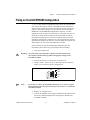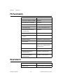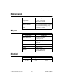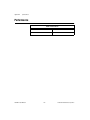
1
PCI-MXI-2
User Manual
January 1996 Edition
Part Number 321032A-01
© Copyright 1996 National Instruments Corporation. All Rights Reserved.
Internet Support
[email protected]
E-mail: [email protected]
FTP Site: ftp.natinst.com
Web Address: http://www.natinst.com
Bulletin Board Support
BBS United States: (512) 794-5422
BBS United Kingdom: 01635 551422
BBS France: 01 48 65 15 59
Fax-on-Demand Support
(512) 418-1111
Telephone Support (U.S.)
Tel: (512) 795-8248
Fax: (512) 794-5678
International Offices
Australia 03 9879 5166, Austria 0662 45 79 90 0, Belgium 02 757 00 20,
Canada (Ontario) 905 785 0085, Canada (Québec) 514 694 8521, Denmark 45 76 26 00,
Finland 09 725 725 11, France 01 48 14 24 24, Germany 089 741 31 30,
Hong Kong 2645 3186, Israel 03 5734815, Italy 02 413091, Japan 03 5472 2970,
Korea 02 596 7456, Mexico 5 520 2635, Netherlands 0348 433466, Norway 32 84 84 00,
Singapore 2265886, Spain 91 640 0085, Sweden 08 730 49 70, Switzerland 056 200 51 51,
Taiwan 02 377 1200, U.K. 01635 523545
National Instruments Corporate Headquarters
6504 Bridge Point Parkway
Austin, TX 78730-5039
Tel: (512) 794-0100
Important Information
Warranty
The PCI-MXI-2 is warranted against defects in materials and workmanship for a period of one year from the date of
shipment, as evidenced by receipts or other documentation. National Instruments will, at its option, repair or replace
equipment that proves to be defective during the warranty period. This warranty includes parts and labor.
The media on which you receive National Instruments software are warranted not to fail to execute programming
instructions, due to defects in materials and workmanship, for a period of 90 days from date of shipment, as evidenced
by receipts or other documentation. National Instruments will, at its option, repair or replace software media that do
not execute programming instructions if National Instruments receives notice of such defects during the warranty
period. National Instruments does not warrant that the operation of the software shall be uninterrupted or error free.
A Return Material Authorization (RMA) number must be obtained from the factory and clearly marked on the outside
of the package before any equipment will be accepted for warranty work. National Instruments will pay the shipping
costs of returning to the owner parts which are covered by warranty.
National Instruments believes that the information in this manual is accurate. The document has been carefully
reviewed for technical accuracy. In the event that technical or typographical errors exist, National Instruments reserves
the right to make changes to subsequent editions of this document without prior notice to holders of this edition. The
reader should consult National Instruments if errors are suspected. In no event shall National Instruments be liable for
any damages arising out of or related to this document or the information contained in it.
EXCEPT AS SPECIFIED HEREIN, NATIONAL INSTRUMENTS MAKES NO WARRANTIES, EXPRESS OR IMPLIED, AND
SPECIFICALLY DISCLAIMS ANY WARRANTY OF MERCHANTABILITY OR FITNESS FOR A PARTICULAR PURPOSE.
CUSTOMER’S RIGHT TO RECOVER DAMAGES CAUSED BY FAULT OR NEGLIGENCE ON THE PART OF NATIONAL
INSTRUMENTS SHALL BE LIMITED TO THE AMOUNT THERETOFORE PAID BY THE CUSTOMER. NATIONAL INSTRUMENTS
WILL NOT BE LIABLE FOR DAMAGES RESULTING FROM LOSS OF DATA, PROFITS , USE OF PRODUCTS, OR INCIDENTAL OR
CONSEQUENTIAL DAMAGES , EVEN IF ADVISED OF THE POSSIBILITY THEREOF. This limitation of the liability of National
Instruments will apply regardless of the form of action, whether in contract or tort, including negligence. Any action
against National Instruments must be brought within one year after the cause of action accrues. National Instruments
shall not be liable for any delay in performance due to causes beyond its reasonable control. The warranty provided
herein does not cover damages, defects, malfunctions, or service failures caused by owner’s failure to follow the
National Instruments installation, operation, or maintenance instructions; owner’s modification of the product;
owner’s abuse, misuse, or negligent acts; and power failure or surges, fire, flood, accident, actions of third parties, or
other events outside reasonable control.
Copyright
Under the copyright laws, this publication may not be reproduced or transmitted in any form, electronic or mechanical,
including photocopying, recording, storing in an information retrieval system, or translating, in whole or in part,
without the prior written consent of National Instruments Corporation.
Trademarks
LabVIEW® and NI-VXI™ are trademarks of National Instruments Corporation.
Product and company names listed are trademarks or trade names of their respective companies.
Warning Regarding Medical and Clinical Use of National Instruments Products
National Instruments products are not designed with components and testing intended to ensure a level of reliability
suitable for use in treatment and diagnosis of humans. Applications of National Instruments products involving
medical or clinical treatment can create a potential for accidental injury caused by product failure, or by errors on the
part of the user or application designer. Any use or application of National Instruments products for or involving
medical or clinical treatment must be performed by properly trained and qualified medical personnel, and all traditional
medical safeguards, equipment, and procedures that are appropriate in the particular situation to prevent serious injury
or death should always continue to be used when National Instruments products are being used. National Instruments
products are NOT intended to be a substitute for any form of established process, procedure, or equipment used to
monitor or safeguard human health and safety in medical or clinical treatment.
FCC/DOC Radio Frequency Interference
Class A Compliance
This equipment generates and uses radio frequency energy and, if not installed and used in strict
accordance with the instructions in this manual, may cause interference to radio and television
reception. Classification requirements are the same for the Federal Communications Commission
(FCC) and the Canadian Department of Communications (DOC). This equipment has been tested and
found to comply with the following two regulatory agencies:
Federal Communications Commission
This equipment has been tested and found to comply with the limits for a Class A digital device,
pursuant to part 15 of the FCC Rules. These limits are designed to provide reasonable protection against
harmful interference when the equipment is operated in a commercial environment. This equipment
generates, uses, and can radiate radio frequency energy and, if not installed and used in accordance with
the instruction manual, may cause harmful interference to radio communications. Operation of this
equipment in a residential area is likely to cause harmful interference in which case the user will be
required to correct the interference at his own expense.
Notices to User:
Changes or modifications not expressly approved by National Instruments could void
the user’s authority to operate the equipment under the FCC Rules.
This device complies with the FCC rules only if used with shielded interface cables of
suitable quality and construction. National Instruments used such cables to test this
device and provides them for sale to the user. The use of inferior or nonshielded
interface cables could void the user’s authority to operate the equipment under the
FCC rules.
If necessary, consult National Instruments or an experienced radio/television technician for additional
suggestions. The following booklet prepared by the FCC may also be helpful: Interference to Home
Electronic Entertainment Equipment Handbook. This booklet is available from the U.S. Government
Printing Office, Washington, DC 20402.
Canadian Department of Communications
This Class A digital apparatus meets all requirements of the Canadian Interference-Causing Equipment
Regulations.
Cet appareil numérique de la classe A respecte toutes les exigences du Règlement sur le matériel
brouilleur du Canada.
Table
of
Contents
About This Manual
Organization of This Manual ........................................................................................ vii
Conventions Used in This Manual................................................................................ viii
Related Documentation................................................................................................. viii
Customer Communication ............................................................................................ viii
Chapter 1
Introduction
PCI-MXI-2 Overview ................................................................................................... 1-1
MXI-2 Description........................................................................................................ 1-2
What You Need to Get Started ..................................................................................... 1-2
Optional Equipment ...................................................................................................... 1-3
Optional Software ......................................................................................................... 1-4
Chapter 2
Functional Overview
PCI-MXI-2 Functional Description .............................................................................. 2-1
Chapter 3
PCI-MXI-2 Configuration and Installation
Configure the PCI-MXI-2............................................................................................. 3-1
Configuration EEPROM ................................................................................ 3-3
Onboard DRAM ............................................................................................. 3-4
MXIbus Termination Option.......................................................................... 3-4
Install the PCI-MXI-2 ................................................................................................... 3-5
Fixing an Invalid EEPROM Configuration .................................................................. 3-7
Appendix A
Specifications
© National Instruments Corporation
v
PCI-MXI-2 User Manual
Table of Contents
Appendix B
MXI-2 Connector
Appendix C
Customer Communication
Glossary
Figures
Figure 2-1.
PCI-MXI-2 Block Diagram................................................................... 2-2
Figure 3-1.
Figure 3-2.
Figure 3-3.
Figure 3-4.
Figure 3-5.
PCI-MXI-2 Parts Locator Diagram ....................................................... 3-2
EEPROM Operation.............................................................................. 3-3
Terminating Resistors and Jumper W1 ................................................. 3-5
PCI-MXI-2 Installed in a Computer...................................................... 3-6
Restoring the Factory Configuration ..................................................... 3-7
Figure B-1.
MXI-2 Connector .................................................................................. B-1
Tables
Table 3-1.
PCI-MXI-2 DRAM Configurations ...................................................... 3-4
Table B-1.
Table B-2.
MXI-2 Connector Signal Assignments ................................................. B-1
MXIbus Signal Characteristics.............................................................. B-3
PCI-MXI-2 User Manual
vi
© National Instruments Corporation
About
This
Manual
The PCI-MXI-2 User Manual describes the functional, physical, and
electrical aspects of the PCI-MXI-2 and contains information
concerning its operation and programming.
Organization of This Manual
The PCI-MXI-2 User Manual is organized as follows:
•
Chapter 1, Introduction, describes the PCI-MXI-2, lists the
contents of your PCI-MXI-2 kit, lists optional equipment and
software, and introduces the concepts of MXI-2.
•
Chapter 2, Functional Overview, contains functional descriptions
of each major logic block on the PCI-MXI-2.
•
Chapter 3, PCI-MXI-2 Configuration and Installation, contains the
instructions to configure and install the PCI-MXI-2 module.
•
Appendix A, Specifications, various module specifications of the
PCI-MXI-2, such as physical dimensions and power requirements.
•
Appendix B, MXI-2 Connector, describes the MXI-2 connector on
the PCI-MXI-2 interface board.
•
Appendix C, Customer Communication, contains forms you can
use to request help from National Instruments or to comment on our
products and manuals.
•
The Glossary contains an alphabetical list and description of terms
used in this manual, including abbreviations, acronyms, metric
prefixes, and symbols.
•
The Index contains an alphabetical list of key terms and topics in
this manual, including the page where you can find each one.
© National Instruments Corporation
vii
PCI-MXI-2 User Manual
About This Manual
Conventions Used in This Manual
The following conventions are used in this manual:
bold italic
Bold italic text denotes a note, caution, or warning.
italic
Italic text denotes emphasis, a cross reference, or an introduction to a
key concept.
monospace
Text in this font denotes text or characters that you should literally enter
from the keyboard, sections of code, programming examples, and
syntax examples. This font is also used for the proper names of disk
drives, paths, directories, programs, subprograms, subroutines, device
names, functions, operations, variables, filenames and extensions, and
for statements and comments taken from programs.
The Glossary lists abbreviations, acronyms, metric prefixes,
mnemonics, symbols, and terms.
Related Documentation
The following documents contain information that you may find helpful
as you read this manual:
•
ANSI/IEEE Standard 1014-1987, IEEE Standard for a Versatile
Backplane Bus: VMEbus
•
ANSI/IEEE Standard 1155-1993, IEEE VMEbus Extensions for
Instrumentation: VXIbus
•
ANSI/VITA 1-1994, VME64
•
Multisystem Extension Interface Bus Specification, Version 2.0
(available from National Instruments Corporation)
•
VXI-6, VXIbus Mainframe Extender Specification, Rev. 1.0, VXIbus
Consortium
Customer Communication
National Instruments wants to receive your comments on our products
and manuals. We are interested in the applications you develop with our
products, and we want to help if you have problems with them. To make
it easy for you to contact us, this manual contains comment and
configuration forms for you to complete. These forms are in
Appendix C, Customer Communication, at the end of this manual.
PCI-MXI-2 User Manual
viii
© National Instruments Corporation
Chapter
1
Introduction
This chapter describes the PCI-MXI-2, lists the contents of your
PCI-MXI-2 kit, lists optional equipment and software, and introduces
the concepts of MXI-2.
PCI-MXI-2 Overview
The PCI-MXI-2 is a half-size, PCI-compatible plug-in circuit board that
plugs into one of the expansion slots in your PCI-based computer. It
links your PCI-based computer directly to the MXIbus and vice versa.
Because the PCI-MXI-2 uses the same communication register set that
other VXIbus message-based devices use, other MXIbus devices view
the PCI-MXI-2 as a VXIbus device. The PCI-MXI-2 can also function
as the MXIbus System Controller and can terminate the MXIbus signals
directly on the PCI-MXI-2. In addition, you can have up to 16 MB of
onboard DRAM on the PCI-MXI-2 that can either be shared with the
MXIbus and VXI/VMEbus, or used as a dedicated data buffer.
The PCI-MXI-2 achieves high performance block transfer rates by
integrating the MITE custom ASIC, a sophisticated dual-channel DMA
controller with standard interfaces for VXI, VME, MXI, and PCI. By
using MITE DMA to transfer data and commands to and from devices,
the MITE frees up a computer’s microprocessor to perform other tasks
such as data analysis and presentation. In addition to DMA, the MITE
incorporates both the new Synchronous MXI protocol and VME64
MBLT (8-byte block transfers in which both the address bus and data
bus are used to transfer data) directly into the ASIC to perform the
fastest transfer operation to instruments.
The PCI-MXI-2 has the following features:
•
Interfaces the PCI bus to the MXIbus (32-bit Multisystem
eXtension Interface bus)
•
Supports D64, block, and synchronous MXI cycles for
high-performance data transfer
•
Directly controls MXIbus interrupt levels, utility signals, TTL
triggers, and CLK10
© National Instruments Corporation
1-1
PCI-MXI-2 User Manual
Chapter 1
Introduction
•
Allows for optional or user-installable onboard DRAM up to
16 MB, which can be shared with the MXIbus
•
Conforms to PCI specification 2.0
•
Conforms to the MXIbus specification 2.0
•
Supports MXI bus termination
MXI-2 Description
MXI-2 is the second generation of the National Instruments MXIbus
product line. The MXIbus is a general-purpose, 32-bit, multimaster
system bus on a cable. MXI-2 expands the number of signals on a
standard MXI cable by including VXI triggers, all VXI interrupts,
CLK10, and all of the utility bus signals (SYSFAIL*, SYSRESET*,
and ACFAIL*).
Because MXI-2 incorporates all of these new signals into a single
connector, the triggers, interrupts, and utility signals can be extended
not only to other mainframes but also to the local CPU in all MXI-2
products using a single cable. Thus, MXI-2 lets CPU interface boards
such as the PCI-MXI-2 perform as though they were plugged directly
into the VXI/VME backplane.
In addition, MXI-2 surpasses the data throughput of
previous-generation MXIbus products by defining new
high-performance protocols. MXI-2 is a superset of MXI. All accesses
initiated by MXIbus devices will work with MXI-2 devices. However,
MXI-2 defines synchronous MXI block data transfers that surpass
previous block data throughput benchmarks. The new synchronous
MXI block protocol increases MXI-2 throughput to a maximum of
33 MB/s between two MXI-2 devices. All National Instruments MXI-2
boards can initiate and respond to synchronous MXI block cycles.
Note:
In the remainder of this manual, the term MXIbus refers to MXI-2.
What You Need to Get Started
❑ PCI-based computer
❑ PCI-MXI-2 interface board
❑ MXI-2 cable
PCI-MXI-2 User Manual
1-2
© National Instruments Corporation
Chapter 1
Introduction
Optional Equipment
•
Type M1 MXI-2 Cables
Straight-point connector to straight-point connector:
–
•
Type M2 MXI-2 Cables
Straight-point connector to right-angle daisy-chain connector:
–
•
1 m, 2 m, 4 m, or 8 m
Type MB-5 MXI-2 Cables
Standard right-angle daisy-chain connector to straight bulkhead
exit connector:
–
© National Instruments Corporation
1 m, 2 m, 4 m, or 8 m
Type MB-4 MXI-2 Cables
Standard right-angle point connector to straight bulkhead entry
connector:
–
•
1 m, 2 m, 4 m, or 8 m
Type MB-3 MXI-2 Cables
Wall-mount bulkhead entry connector to straight right-angle
daisy-chain connector:
–
•
1 m, 2 m, 4 m, or 8 m
Type MB-2 MXI-2 Cables
Straight bulkhead exit connector to straight bulkhead entry
connector:
–
•
1 m, 2 m, 4 m, 8 m, or 20 m
Type MB-1 MXI-2 Cables
Standard right-angle point connector to wall-mount bulkhead exit
connector:
–
•
1 m, 2 m, 4 m, 8 m, or 20 m
Type M4 MXI-2 Cables
Straight-point connector to reverse right-angle daisy-chain
connector:
–
•
1 m, 2 m, 4 m, 8 m, or 20 m
Type M3 MXI-2 Cables
Right-angle point connector to right-angle daisy-chain connector:
–
•
1 m, 2 m, 4 m, 8 m, or 20 m
1 m, 2 m, 4 m, or 8 m
1-3
PCI-MXI-2 User Manual
Chapter 1
Introduction
•
Type MB-6 MXI-2 Cables
Reverse right-angle daisy-chain connector to wall-mount bulkhead
exit connector:
–
•
1 m, 2 m, 4 m, or 8 m
Onboard DRAM
–
4 MB or 16 MB
Optional Software
You can order the National Instruments NI-VXI bus interface software
for the PCI-MXI-2. The NI-VXI software includes a Resource
Manager, graphical and text-based versions of an interactive VXI
resource editor program, a comprehensive library of software routines
for VXI/VME programming, and graphical and text-based versions of
an interactive control program for interacting with VXI/VME. You
can use this software to seamlessly program multiple-mainframe
configurations and have software compatibility across a variety of
VXI/VME controller platforms.
In addition to NI-VXI, you can order the National Instruments
LabVIEW and LabWindows®/CVI application programs and
instrument drivers to ease your programming task. These standardized
programs match the modular virtual instrument capability of VXI and
can reduce your VXI/VMEbus software development time. These
programs are fully VXIplug&play compliant and feature extensive
libraries of VXI instrument drivers written to take full advantage of
direct VXI control.
LabVIEW is a complete programming environment that departs from
the sequential nature of traditional programming languages and features
a graphical programming environment.
LabWindows/CVI is an interactive C development environment for
building test and measurement and instrument control systems. It
includes interactive code-generation tools and a graphical editor for
building custom user interfaces.
LabVIEW and LabWindows/CVI include all the tools needed for
instrument control, data acquisition, analysis, and presentation. When
you order the LabVIEW VXI Development System for Windows or the
LabWindows/CVI VXI Development System for Windows, you also
PCI-MXI-2 User Manual
1-4
© National Instruments Corporation
Chapter 1
Introduction
get more than 500 complete instrument drivers, which are modular,
source-code programs that handle the communication with your
instrument to speed your application development.
© National Instruments Corporation
1-5
PCI-MXI-2 User Manual
Chapter
Functional Overview
2
This chapter contains functional descriptions of each major logic block
on the PCI-MXI-2.
PCI-MXI-2 Functional Description
In the simplest terms, you can think of the PCI-MXI-2 as a bus
translator that converts PCI bus signals into appropriate MXIbus
signals. From the perspective of the MXIbus, the PCI-MXI-2
implements a MXIbus interface to communicate with other MXIbus
devices. From the perspective of the PCI bus, the PCI-MXI-2 is an
interface to the outside world.
Figure 2-1 is a functional block diagram of the PCI-MXI-2. Following
the diagram is a description of each logic block shown.
© National Instruments Corporation
2-1
PCI-MXI-2 User Manual
Chapter 2
Functional Overview
PCI Bus Slave
State Machine
Programmable
Outward
Windows
Base Address
Registers
DMA (1)
PCI Bus Master
State Machine
DMA (2)
MXIbus Master
State Machine
MXIbus Parity
Check and
Generation
A24/A32
Decoder
PCI-MXI-2
Registers
LA
Decoder
MXIbus Slave
State Machine
MXI Bus
PCI Bus
Onboard DRAM
SIMM
MXIbus
Terminate
MXIbus System
Controller Functions
MXIbus Bus
Timeout Unit
Interrupt
Circuitry
Trigger
Circuitry
Utility Signal
Circuitry
Figure 2-1. PCI-MXI-2 Block Diagram
PCI-MXI-2 User Manual
• PCI Bus Slave
State Machine
This state machine monitors the output of the
window decoders and responds to PCI bus
cycles that are intended for the PCI-MXI-2. The
cycles may map to the PCI-MXI-2 registers, the
onboard DRAM, or the MXIbus. The
PCI-MXI-2 is a medium-speed PCI decoder
that accepts both configuration and memory
cycles. The interface logic ensures that the
PCI-MXI-2 meets the loading, driving, and
timing requirements of the PCI specification.
• Base Address
Registers
The PCI-MXI-2 using PCI registers BAR0l
destination of PCI cycles that match the base
address registers is determined by the
programmable outward windows.
2-2
© National Instruments Corporation
Chapter 2
Functional Overview
• Programmable
Outward Windows
The PCI-MXI-2 has multiple programmable
outward windows. These windows direct the
PCI slave state machine to route incoming
cycles to local registers, onboard DRAM, or to
the MXIbus.
• MXIbus Master
State Machine
This state machine generates MXIbus master
data transfer cycles when directed to do so by
the PCI bus slave state machine, thus allowing
PCI bus cycles to map to the MXIbus. The
PCI-MXI-2 can generate D64, D32, D16, and
D08(EO) single, block, and RMW cycles on
MXIbus in A32 and A24 space (D64 is
performed by doing successive D32 transfers).
All data transfers can also be generated in A16
space with the exception of D64 and block
transfers. The MXIbus master state machine
also checks MXIbus parity on read data
received and stores an error status when a parity
error is detected. The transceivers ensure that
the PCI-MXI-2 meets the loading, driving, and
timing requirements of the MXIbus
specification for the AD[31–0], AM[4–0], and
CONVERT* signals.
• PCI Bus Master
State Machine
This state machine generates PCI bus master
data transfer cycles when directed to do so by
the MXIbus slave state machine or one of the
DMA controllers on the PCI-MXI-2. The
PCI-MXI-2 can generate 8-, 16-, and 32-bit
memory read and write cycles (both single and
multiple). The PCI-MXI-2 will not generate
unaligned PCI bus data transfers. The interface
logic ensures that the PCI-MXI-2 meets the
loading, driving, and timing requirements of the
PCI specification.
• DMA Controllers
The PCI-MXI-2 has two independent onboard
DMA controllers. The DMA controllers are
capable of transferring data at maximum speeds
between any combination of the PCIbus,
onboard DRAM, or MXIbus.
© National Instruments Corporation
2-3
PCI-MXI-2 User Manual
Chapter 2
Functional Overview
PCI-MXI-2 User Manual
• MXIbus Parity
Check and
Generation
The MXIbus parity check/generation circuitry
checks for even parity at anytime that the
PCI-MXI-2 is receiving the AD[31–0] signals.
If parity is not even, the appropriate MXIbus
state machine is signaled. The MXIbus master
state machine is signaled for a parity error
during the data phase of a MXIbus master read
cycle, while the MXIbus slave state machine is
signaled for a parity error during the address
phase of any MXIbus slave cycle and the data
phase of a MXIbus slave write cycle. Even
parity is also generated and sent to the MXIbus
with master address and write data as well as
slave read data.
• Onboard DRAM
SIMM
This logic block represents the DRAM SIMM
socket on the PCI-MXI-2. If DRAM is
installed, it will be accessible in the PCI-MXI-2
A24/A32 memory space.
• PCI-MXI-2
Registers
This logic block represents all registers on the
PCI-MXI-2. The registers are accessible from
either the PCI bus or MXIbus. All registers are
available from the PCI bus, while a subset is
accessible in the PCI-MXI-2 MXIbus A16
configuration area.
• A24/A32 Decoder
This address decoder monitors the MXIbus for
access to the PCI-MXI-2 A24/A32 memory
space. All resources located on the PCI-MXI-2
are accessible in this region. The decoded
region can be routed to the PCI bus or onboard
DRAM SIMM.
• Logical Address
Decoder
This address decoder monitors the MXIbus for
A16 accesses to the PCI-MXI-2 MXIbus
configuration space registers based on its
logical address. A subset of the PCI-MXI-2
registers is accessible in this region.
2-4
© National Instruments Corporation
Chapter 2
Functional Overview
• MXIbus Slave
State Machine
This state machine monitors the output of the
address decoders and responds to MXIbus
cycles that are intended for the PCI-MXI-2.
Cycles that map to the Logical Address decoder
access the PCI-MXI-2 registers, while cycles
that map to the A24/A32 decoder access either
the PCI-MXI-2 registers or the onboard DRAM
SIMM. The PCI-MXI-2 can accept D32, D16,
and D08(EO) single and RMW MXIbus cycles
in A32, A24, and A16 space. The PCI-MXI-2
can also accept synchronous and block MXIbus
cycles in A32 and A24 space. The MXIbus
slave state machine checks for MXIbus parity
errors. If a parity error is detected during the
address phase of a cycle, the PCI-MXI-2
ignores the cycle. If a parity error is detected
during the data phase of write cycle, the
MXIbus slave state machine responds with a
BERR* on the MXIbus. The transceivers
ensure that the PCI-MXI-2 meets the loading,
driving, and timing requirements of the
MXIbus specification for the AD[31–0],
AM[4–0], and CONVERT* signals.
• MXIbus Terminate
The PCI-MXI-2 has onboard MXIbus
termination to terminate the MXIbus signals if
it is at either end of the cable. If the PCI-MXI-2
is a middle device on the MXIbus, the
termination should be disabled.
• MXIbus System
Controller
Functions
The PCI-MXI-2 has the ability to act as the
MXIbus system controller. When acting as the
system controller, the PCI-MXI-2 provides the
MXIbus arbiter, priority-selection daisy-chain
driver, and bus timeout unit. The PCI-MXI-2
can automatically detect from the MXIbus
cable if it is the system controller.
© National Instruments Corporation
2-5
PCI-MXI-2 User Manual
Chapter 2
Functional Overview
PCI-MXI-2 User Manual
• MXIbus Bus
Timeout Unit
The PCI-MXI-2 has a MXIbus bus timeout
unit, which terminates (with BERR*) any
MXIbus cycle in which DTACK* or BERR*
are not asserted in a prescribed amount of time
after DS* is asserted. The duration of the
timeout is programmably selectable in the
range of 30 µs to 500 ms.
• Interrupt, Trigger,
and Utility Signal
Circuitry
This circuitry handles mapping of the interrupt,
trigger, and utility signals to the MXIbus.
The utility signals include SYSRESET*,
SYSFAIL*, and ACFAIL*. This circuitry also
generates interrupts from other conditions on
the PCI-MXI-2 and allows generation of the
trigger or utility signals. The transceivers
ensure that the PCI-MXI-2 meets the loading,
driving, and timing requirements of the
MXIbus specification for the IRQ[7:1], gnals.
2-6
© National Instruments Corporation
PCI-MXI-2 Configuration
and Installation
Chapter
3
This chapter contains the instructions to configure and install the
PCI-MXI-2 module.
Warning: Electrostatic discharge can damage several components on your
PCI-MXI-2 module. To avoid such damage in handling the module, touch
the antistatic plastic package to a metal part of your computer chassis
before removing the PCI-MXI-2 from the package.
Configure the PCI-MXI-2
This section describes how to configure the following options on the
PCI-MXI-2:
•
Configuration EEPROM
•
Onboard DRAM
•
MXI-2 termination
Figure 3-1 shows the PCI-MXI-2. The drawing shows the location and
factory-default settings on the module.
© National Instruments Corporation
3-1
PCI-MXI-2 User Manual
Chapter 3
PCI-MXI-2 Configuration and Installation
1
2
3
4
1
W1
2
Termination Circuitry
3
DRAM
4
U17
Figure 3-1. PCI-MXI-2 Parts Locator Diagram
PCI-MXI-2 User Manual
3-2
© National Instruments Corporation
Chapter 3
PCI-MXI-2 Configuration and Installation
Configuration EEPROM
The PCI-MXI-2 has an onboard EEPROM, which stores default register
values that are loaded at power-on. The EEPROM is divided into two
halves—a factory-configuration half, and a user-configuration half so
you can modify the user-configurable half, while the factory-configured
half stores a back-up of the default user settings. The factory
configuration is a minimal configuration that allows you to boot your
PCI-MXI-2 regardless of the changes made to the user configuration.
Use switch 1 (FOV) of the four-position switch at location U17
to control the operation of the EEPROM. Switch 1 determines
whether the PCI-MXI-2 boots off the factory-configured half or the
user-configurable half. In its default setting, the PCI-MXI-2 boots off
the user-configurable half. This switch is useful for restoring the
user-configured half of the EEPROM to the factory configuration
values in the event that it becomes corrupted in such a way that the
PCI-MXI-2 boots to an unusable state. See the Fixing an Invalid
EEPROM Configuration section later in this chapter for more details on
using switch 1.
The TST switch (switch 2 of U17) lets you change the default factory
configuration settings by permitting writes to the factory settings
section of the EEPROM. This switch serves as a safety measure and
should not be needed under normal circumstances. When this switch is
off (its default setting) the factory configuration of the EEPROM is
protected so any writes to the factory area will be ignored. The factory
area is protected regardless of the setting of switch 1 of U17.
Figure 3-2 shows the default configuration settings for EEPROM
operation.
!
Caution:
Do not alter the settings of switches 3 and 4 of U17. Leave these switches
as shown in Figure 3-2 unless specifically directed by National
Instruments.
U17
FOV
ON
1 2 3 4
TST
POS
CT
Figure 3-2. EEPROM Operation
© National Instruments Corporation
3-3
PCI-MXI-2 User Manual
Chapter 3
PCI-MXI-2 Configuration and Installation
Onboard DRAM
The PCI-MXI-2 can accommodate one DRAM SIMM. Table 3-1 lists
the SIMMS you can use. You can use 32-bit or 36-bit SIMMS since
DRAM parity is not required. The PCI-MXI-2 can hold up to 16 MB of
onboard memory. The PCI-MXI-2 supports DRAM speeds of 80 ns or
faster.
Table 3-1. PCI-MXI-2 DRAM Configurations
SIMMs
Total DRAM
National Instruments Option?
—
0
—
256K x 32 or
256K x 36
1 MB
—
1M x 32 or
1M x 36
4 MB
YES
4M x 32 or
4M x 36
16 MB
YES
MXIbus Termination Option
The MXIbus requires that the first and last devices in the daisy-chain
have a termination network. The PCI-MXI-2 has the ability to terminate
the MXIbus signals on the interface board using terminating resistor
networks in single inline packages (SIPs). Only the first and last devices
in the MXIbus daisy-chain should be terminated.
The onboard termination option lets you install or remove terminating
resistor networks from their sockets on the PCI-MXI-2 board. The
board is shipped from the factory with these terminating resistor
networks installed. If your PCI-MXI-2 is to be the first or last device
in the MXIbus daisy-chain, leave these internal resistor terminators in
place. The jumper on the pins at W1 should also be in place when the
PCI-MXI-2 is an end device.
If the PCI-MXI-2 is not going to be an end device on the MXIbus
daisy-chain, remove both the jumper from the pins at W1 as well as all
of the internal terminating resistor networks from their sockets. Store
them in a safe place in case the MXIbus system configuration changes.
When reinstalling the resistor networks, ensure that they are plugged
firmly into their respective sockets.
PCI-MXI-2 User Manual
3-4
© National Instruments Corporation
Chapter 3
PCI-MXI-2 Configuration and Installation
Figure 3-3 shows the location of the terminating resistors and the
W1 jumper. The figure shows the resistors and the jumper installed
for use as an end device.
1
2
1
W1 Jumper
2
Termination Resistors
Figure 3-3. Terminating Resistors and Jumper W1
Install the PCI-MXI-2
This section contains general installation instructions for the
PCI-MXI-2. Consult your computer user manual or technical reference
manual for specific instructions and warnings.
1.
Plug in your PCI-based computer before installing the PCI-MXI-2.
The power cord grounds the computer and protects it from
electrical damage while you are installing the module.
Warning: To protect both yourself and the computer from electrical hazards, the
computer should remain off until you are finished installing the
PCI-MXI-2 module.
2.
Remove the top cover or access port to the PCI bus.
3.
Select any available PCI expansion slot.
© National Instruments Corporation
3-5
PCI-MXI-2 User Manual
Chapter 3
PCI-MXI-2 Configuration and Installation
4.
Locate the metal bracket that covers the cut-out in the back panel
of the chassis for the slot you have selected. Remove and save the
bracket-retaining screw and the bracket cover.
5.
Touch the metal part of the power supply case inside the computer
to discharge any static electricity that might be on your clothes or
body.
6.
Line up the PCI-MXI-2 with the MXI-2 connector near the cut-out
on the back panel. Slowly push down on the top of the PCI-MXI-2
until its card-edge connector is resting on the expansion slot
receptacle. Using slow, evenly distributed pressure, press the
PCI-MXI-2 straight down until it seats in the expansion slot.
7.
Reinstall the bracket-retaining screw to secure the PCI-MXI-2 to
the back panel rail.
8.
Check the installation.
9.
Replace the computer cover.
Figure 3-4 shows how to install the PCI-MXI-2.
5
4
3
2
1
1
4
PCI Bus Slot
MXI-2 Connector
2
5
Cut-outs
PCI-MXI-2 Board
3
PCI Bus Card-Edge Connector
Figure 3-4. PCI-MXI-2 Installed in a Computer
PCI-MXI-2 User Manual
3-6
© National Instruments Corporation
Chapter 3
PCI-MXI-2 Configuration and Installation
Fixing an Invalid EEPROM Configuration
VXIEDIT is the software configuration utility in the NI-VXI software.
You can use this utility to edit the configuration of the PCI-MXI-2.
Some of these settings are stored in files that are read by the NI-VXI
software, while other settings are stored directly in the PCI-MXI-2
EEPROM. Certain EEPROM configurations can cause your PCI
computer to lock up while in its boot process. Generally, only the size
and location of the memory windows can cause problems with the
PCI-MXI-2 locking up your system. For example, many PCI-based
computers will not boot if a board in its system requests more memory
space than the computer can allocate. If you encounter this situation you
should reduce the size of the PCI-MXI-2 user window.
If this situation occurs after changing the configuration on the
PCI-MXI-2, follow these steps to reconfigure the PCI-MXI-2.
1.
Turn your computer off.
Warning: To protect both yourself and the computer from electrical hazards,
the computer should remain off while changing the settings on the
PCI-MXI-2 module.
2.
Remove the top cover or access port to the PCI bus.
3.
Change switch 1 (FOV) on U17 to the ON position as shown in
Figure 3-5 to restore the factory configuration.
U17
FOV
ON
1 2 3 4
TST
POS
CT
Figure 3-5. Restoring the Factory Configuration
Note:
If you have to remove the PCI-MXI-2 module to access switch 1, follow
the installation instructions given in the previous section to re-install the
PCI-MXI-2 module.
4.
Replace the computer cover.
5.
Turn on the computer. The computer should boot this time because
the factory-default configuration is being used to initialize the
PCI-MXI-2 module.
© National Instruments Corporation
3-7
PCI-MXI-2 User Manual
Chapter 3
PCI-MXI-2 Configuration and Installation
6.
Run the NI-VXI utility VXIEDIT to re-adjust the PCI-MXI-2
configuration. Refer to the NI-VXI Graphical Utilities Reference
Manual for instructions on using this utility.
7.
After saving the configuration, exit Windows and turn off the
computer.
8.
Remove the top cover or access port to the PCI bus.
9.
Change switch 1 (FOV) on U17 to the OFF position.
10. Replace the computer cover.
11. Turn on the computer. If the computer does not boot with this
configuration, you will have to repeat these steps, modifying your
configuration until a final configuration is reached.
PCI-MXI-2 User Manual
3-8
© National Instruments Corporation
Appendix
A
Specifications
This appendix lists various module specifications of the PCI-MXI-2,
such as physical dimensions and power requirements.
MXIbus Capability Descriptions
•
Master-mode A32, A24, and A16 addressing
•
Master-mode block transfers and synchronous block transfers
•
Slave-mode A32, A24, and A16 addressing
•
Slave-mode block transfers and synchronous block transfers
•
Master-mode D32, D16, and D08 data sizes
•
Slave-mode D32, D16, and D08 data sizes
•
Optional MXIbus System Controller
•
Can be a fair MXIbus requester
•
Can lock the MXIbus for indivisible transfers
•
Can terminate the MXIbus
•
MXIbus master retry support
•
MXIbus slave retry support
•
Interrupt handler for levels 7 to 1
•
Interrupt requester for levels 7 to 1
•
MXIbus D32, D16, D08(O) interrupt handler
•
MXIbus D32, D16, D08(O) interrupter
•
Release on Acknowledge or Register Access interrupter
•
MXIbus bus timer (programmable limit)
•
Automatic MXIbus System Controller detection
© National Instruments Corporation
A-1
PCI-MXI-2 User Manual
Appendix A
Specifications
PCI Functionality
Characteristic
Specification
PCI Initiator (Master) Capability
Supported
PCI Target (Slave) Capability
Supported
Data Path
32 bits
Card Voltage/Type
5 V only; 32-bit half-size card
Parity Generation/Checking,
Error Reporting
Supported
Target Decode Speed
Medium (1 clock)
Target Fast-Back-to-Back
Capability
Supported
Resource Locking
Supported as a master and slave
PCI Interrupts
Interrupts passed on INTA# signal
Base Address Registers
BAR 0 dedicated to local registers
BAR 1-3 size configurable from
256 B to 4 GB
Expansion ROM
8 KB
PCI Master Performance
(Ideal Maximum)
132 MB/s (16 Dwords max.)
PCI Slave Performance
(Ideal Maximum)
33 MB/s (to local registers)
Requirements
Characteristic
Memory Space
PCI-MXI-2 User Manual
Specification
32 KB minimum, programmable
A-2
© National Instruments Corporation
Appendix A
Specifications
Environmental
Characteristic
Specification
Temperature
0° to 55° C operating;
–40° to 85° C storage
Relative Humidity
0% to 95% noncondensing, operating;
0% to 95% noncondensing, storage
EMI
FCC Class A Verified
Physical
Characteristic
Specification
Board Dimensions
174.63 by 106.68 mm
(6.875 by 4.2 in.)
Connectors
Single fully implemented MXI-2
connector
Slot Requirements
Single PCI slot
MTBF
Contact factory
Weight
0.18 Kg (0.4 lb) typical
(no DRAM installed)
Electrical
© National Instruments Corporation
Source
Typical
Direct Current (Max)
+5 VDC
2.2 A
2.2 A
A-3
PCI-MXI-2 User Manual
Appendix A
Specifications
Performance
MXI Transfer Rate
PCI-MXI-2 User Manual
Peak
33 MB/s
Sustained
23 MB/s
A-4
© National Instruments Corporation
Appendix
B
MXI-2 Connector
This appendix describes the MXI-2 connector on the PCI-MXI-2
interface board.
The MXI-2 connector is a 144-pin female connector manufactured by
Meritec (Meritec part number 182800A-01). The mating cable
assembly is National Instruments part number 182801A-xxx, where xxx
is the length in meters.
Figure B-1 shows the MXI-2 connector on the PCI-MXI-2. The
drawing shows the pinout assignments for each pin, which are described
in Table B-1.
A35 A33 A31 A29 A27 A25 A23 A21 A19 A17 A15 A13 A11 A9 A7 A5 A3 A1
A36 A34 A32 A30 A28 A26 A24 A22 A20 A18 A16 A14 A12 A10 A8 A6 A4 A2
B35 B33 B31 B29 B27 B25 B23 B21 A19 B17 B15 B13 B11 B9 B7 B5 B3 B1
B36 B34 B32 B30 B28 B26 B24 B22 B20 B18 B16 B14 B12 B10 B8 B6 B4 B2
C35 C33 C31 C29 C27 C25 C23 C21 C19 C17 C15 C13 C11 C9
C7
C36 C34 C32 C30 C28 C26 C24 C22 C20 C18 C16 C14 C12 C10 C8
C5
C6
C3
C4
C1
C2
D35 D33 D31 D29 D27 D25 D23 D21 D19 D17 D15 D13 D11 D9 D7 D5 D3 D1
D36 D34 D32 D30 D28 D26 D24 D22 D20 D18 D16 D14 D12 D10 D8 D6 D4 D2
Figure B-1. MXI-2 Connector
Table B-1 lists the signal assignments for the MXI-2 connector.
Table B-1. MXI-2 Connector Signal Assignments
Pin
Signal Name
Pin
A1
AD(31)*
B1
A2
GND
A3
Pin
Signal Name
Pin
Signal Name
AD(14)*
C1
AM(4)*
D1
BUSY*
B2
GND
C2
GND
D2
GND
AD(30)*
B3
AD(13)*
C3
AM(3)*
D3
IRQ(1)*
A4
GND
B4
GND
C4
GND
D4
GND
A5
AD(29)*
B5
AD(12)*
C5
AM(2)*
D5
IRQ(2)*
© National Instruments Corporation
Signal Name
B-1
PCI-MXI-2 User Manual
Appendix B
MXI-2 Connector
Table B-1. MXI-2 Connector Signal Assignments (Continued)
Pin
Signal Name
Pin
Signal Name
Pin
Signal Name
Pin
Signal Name
A6
GND
B6
GND
C6
GND
D6
GND
A7
AD(28)*
B7
AD(11)*
C7
AM(1)*
D7
IRQ(3)*
A8
GND
B8
GND
C8
GND
D8
GND
A9
AD(27)*
B9
AD(10)*
C9
AM(0)*
D9
IRQ(4)*
A10
GND
B10
GND
C10
GND
D10
GND
A11
AD(26)*
B11
AD(9)*
C11
WR*
D11
IRQ(5)*
A12
GND
B12
GND
C12
GND
D12
GND
A13
AD(25)*
B13
AD(8)*
C13
SIZE*
D13
IRQ(6)*
A14
GND
B14
GND
C14
GND
D14
GND
A15
AD(24)*
B15
AD(7)*
C15
DISBTO*
D15
IRQ(7)*
A16
GND
B16
GND
C16
GND
D16
GND
A17
AD(23)*
B17
AD(6)*
C17
ACFAIL*
D17
TRG(0)+
A18
GND
B18
GND
C18
GND
D18
TRG(0)-
A19
AD(22)*
B19
AD(5)*
C19
SYSRESET*
D19
TRG(1)+
A20
GND
B20
GND
C20
GND
D20
TRG(1)-
A21
AD(21)*
B21
AD(4)*
C21
SYSFAIL*
D21
TRG(2)+
A22
GND
B22
GND
C22
GND
D22
TRG(2)-
A23
AD(20)*
B23
AD(3)*
C23
BERR*
D23
TRG(3)+
A24
GND
B24
GND
C24
GND
D24
TRG(3)-
A25
AD(19)*
B25
AD(2)*
C25
DTACK*
D25
TRG(4)+
A26
GND
B26
GND
C26
GND
D26
TRG(4)-
A27
AD(18)*
B27
AD(1)*
C27
DS*
D27
TRG(5)+
PCI-MXI-2 User Manual
B-2
© National Instruments Corporation
Appendix B
MXI-2 Connector
Table B-1. MXI-2 Connector Signal Assignments (Continued)
Pin
Signal Name
Pin
Signal Name
Pin
Signal Name
Pin
Signal Name
A28
GND
B28
GND
C28
GND
D28
TRG(5)-
A29
AD(17)*
B28
AD(0)*
C29
AS*
D29
TRG(6)+
A30
GND
B30
GND
C30
GND
D30
TRG(6)-
A31
AD(16)*
B31
CONVERT*
C31
BREQ*
D31
TRG(7)+
A32
GND
B32
GND
C32
GND
D32
TRG(7)-
A33
AD(15)*
B33
PAR*
C33
GIN*
D33
CLK10+
A34
GND
B34
GND
C34
GND
D34
CLK10-
A35
5V
B35
TERMPOWER
C35
GOUT*
D35
MXISC*
A36
5V
B36
TERMPOWER
C36
GND
D36
ENDDEV
The characteristic impedance of the MXIbus signals is 120 itional
characteristics of the MXIbus signals.
Table B-2. MXIbus Signal Characteristics
© National Instruments Corporation
Signal
Category
Voltage
Range
Each single-ended
signal
0 to 3.4 V
60 mA
DC to 10 Mhz
Each differential
signal (D17–D34)
0 to 5 V
80 mA
DC to 10 Mhz
Each 5 V (A35, A36)
5V
1.75 A fused
DC
Each
TERMPOWER
(B35, B36)
3.4 V
1.75 A fused
DC
B-3
Max
Current
Frequency
Range
PCI-MXI-2 User Manual
Appendix
Customer Communication
C
For your convenience, this appendix contains forms to help you gather the information necessary to
help us solve your technical problems and a form you can use to comment on the product
documentation. When you contact us, we need the information on the Technical Support Form and the
configuration form, if your manual contains one, about your system configuration to answer your
questions as quickly as possible.
National Instruments has technical assistance through electronic, fax, and telephone systems to
quickly provide the information you need. Our electronic services include a bulletin board service,
an FTP site, a Fax-on-Demand system, and e-mail support. If you have a hardware or software
problem, first try the electronic support systems. If the information available on these systems
does not answer your questions, we offer fax and telephone support through our technical support
centers, which are staffed by applications engineers.
Electronic Services
Bulletin Board Support
National Instruments has BBS and FTP sites dedicated for 24-hour support with a collection of files
and documents to answer most common customer questions. From these sites, you can also download
the latest instrument drivers, updates, and example programs. For recorded instructions on how to use
the bulletin board and FTP services and for BBS automated information, call (512) 795-6990. You can
access these services at:
United States: (512) 794-5422
Up to 14,400 baud, 8 data bits, 1 stop bit, no parity
United Kingdom: 01635 551422
Up to 9,600 baud, 8 data bits, 1 stop bit, no parity
France: 01 48 65 15 59
Up to 9,600 baud, 8 data bits, 1 stop bit, no parity
FTP Support
To access our FTP site, log on to our Internet host, ftp.natinst.com, as anonymous and use your
Internet address, such as [email protected], as your password. The support files and
documents are located in the /support directories.
© National Instruments Corporation
C-1
PCI-MXI-2 User Manual
Fax-on-Demand Support
Fax-on-Demand is a 24-hour information retrieval system containing a library of documents on a wide
range of technical information. You can access Fax-on-Demand from a touch-tone telephone at
(512) 418-1111.
E-Mail Support (currently U.S. only)
You can submit technical support questions to the applications engineering team through e-mail at the
Internet address listed below. Remember to include your name, address, and phone number so we can
contact you with solutions and suggestions.
[email protected]
Telephone and Fax Support
National Instruments has branch offices all over the world. Use the list below to find the technical
support number for your country. If there is no National Instruments office in your country, contact the
source from which you purchased your software to obtain support.
Telephone
Australia
Austria
Belgium
Canada (Ontario)
Canada (Quebec)
Denmark
Finland
France
Germany
Hong Kong
Israel
Italy
Japan
Korea
Mexico
Netherlands
Norway
Singapore
Spain
Sweden
Switzerland
Taiwan
U.K.
03 9879 5166
0662 45 79 90 0
02 757 00 20
905 785 0085
514 694 8521
45 76 26 00
09 725 725 11
01 48 14 24 24
089 741 31 30
2645 3186
03 5734815
02 413091
03 5472 2970
02 596 7456
5 520 2635
0348 433466
32 84 84 00
2265886
91 640 0085
08 730 49 70
056 200 51 51
02 377 1200
01635 523545
Fax
03 9879 6277
0662 45 79 90 19
02 757 03 11
905 785 0086
514 694 4399
45 76 26 02
09 725 725 55
01 48 14 24 14
089 714 60 35
2686 8505
03 5734816
02 41309215
03 5472 2977
02 596 7455
5 520 3282
0348 430673
32 84 86 00
2265887
91 640 0533
08 730 43 70
056 200 51 55
02 737 4644
01635 523154
Technical Support Form
Photocopy this form and update it each time you make changes to your software or hardware, and use
the completed copy of this form as a reference for your current configuration. Completing this form
accurately before contacting National Instruments for technical support helps our applications
engineers answer your questions more efficiently.
If you are using any National Instruments hardware or software products related to this problem,
include the configuration forms from their user manuals. Include additional pages if necessary.
Name __________________________________________________________________________
Company _______________________________________________________________________
Address ________________________________________________________________________
_______________________________________________________________________________
Fax (___ )___________________ Phone (___ ) ________________________________________
Computer brand ________________ Model ________________ Processor___________________
Operating system (include version number) ____________________________________________
Clock speed ______MHz RAM _____MB
Mouse ___yes ___no
Display adapter __________________________
Other adapters installed _______________________________________
Hard disk capacity _____MB
Brand _____________________________________________
Instruments used _________________________________________________________________
_______________________________________________________________________________
National Instruments hardware product model __________ Revision ______________________
Configuration ___________________________________________________________________
National Instruments software product ____________________________ Version ____________
Configuration ___________________________________________________________________
The problem is: __________________________________________________________________
_______________________________________________________________________________
_______________________________________________________________________________
_______________________________________________________________________________
_______________________________________________________________________________
List any error messages: ___________________________________________________________
_______________________________________________________________________________
_______________________________________________________________________________
The following steps reproduce the problem:____________________________________________
_______________________________________________________________________________
_______________________________________________________________________________
_______________________________________________________________________________
_______________________________________________________________________________
_______________________________________________________________________________
Hardware and Software Configuration Form
Record the settings and revisions of your hardware and software on the line to the right of each item.
Complete a new copy of this form each time you revise your software or hardware configuration, and
use this form as a reference for your current configuration. Completing this form accurately before
contacting National Instruments for technical support helps our applications engineers answer your
questions more efficiently.
National Instruments Products
PCI-MXI-2 module part number _____________________________________________________
Serial number ____________________________________________________________________
Revision number _________________________________________________________________
MXIbus Terminators and W1 Jumper Installed or Removed _______________________________
EEPROM Operation (U17 switches 1 and 2) ____________________________________________
DRAM SIMMs Installed ___________________________________________________________
National Instruments Software _______________________________________________________
Other Products
Computer make and model _________________________________________________________
Mainframe make and model _________________________________________________________
Microprocessor ___________________________________________________________________
Clock frequency or speed ___________________________________________________________
Type of video board installed ________________________________________________________
Operating system version ___________________________________________________________
Operating system mode ____________________________________________________________
Other MXIbus devices in system _____________________________________________________
________________________________________________________________________________
Other VXIbus devices in system _____________________________________________________
________________________________________________________________________________
Base I/O address of other boards _____________________________________________________
DMA channels of other boards ______________________________________________________
Interrupt level of other boards _______________________________________________________
VXIbus/MXIbus Resource Manager (make, model, version, software version) _________________
________________________________________________________________________________
Documentation Comment Form
National Instruments encourages you to comment on the documentation supplied with our products.
This information helps us provide quality products to meet your needs.
Title:
PCI-MXI-2 User Manual
Edition Date:
January 1996
Part Number:
321032A-01
Please comment on the completeness, clarity, and organization of the manual.
_______________________________________________________________________________
_______________________________________________________________________________
_______________________________________________________________________________
_______________________________________________________________________________
_______________________________________________________________________________
_______________________________________________________________________________
_______________________________________________________________________________
If you find errors in the manual, please record the page numbers and describe the errors.
_______________________________________________________________________________
_______________________________________________________________________________
_______________________________________________________________________________
_______________________________________________________________________________
_______________________________________________________________________________
_______________________________________________________________________________
_______________________________________________________________________________
Thank you for your help.
Name _________________________________________________________________________
Title __________________________________________________________________________
Company _______________________________________________________________________
Address ________________________________________________________________________
_______________________________________________________________________________
Phone (___ )__________________________ Fax (___ ) _________________________________
Mail to: Technical Publications
National Instruments Corporation
6504 Bridge Point Parkway
Austin, TX 78730-5039
Fax to:
Technical Publications
National Instruments Corporation
(512) 794-5678
Glossary
Prefix
Meanings
Value
n-
nano-
10-9
µ-
micro-
10-6
m-
milli-
10-3
K-
kilo-
103
M-
mega-
106
G-
giga-
109
Symbols
°
degrees
Ω
ohms
%
percent
A
A
amperes
A16 space
VXIbus address space equivalent to the VME 64 KB short address
space. In VXI, the upper 16 KB of A16 space is allocated for use by
VXI devices configuration registers. This 16 KB region is referred to as
VXI configuration space.
A24 space
VXIbus address space equivalent to the VME 16 MB standard address
space.
© National Instruments Corporation
G-1
PCI-MXI-2 User Manual
Glossary
A32 space
VXIbus address space equivalent to the VME 4 GB extended address
space.
ACFAIL
A VMEbus backplane signal that is asserted when a power failure has
occurred (either AC line source or power supply malfunction), or if it is
necessary to disable the power supply (such as for a high temperature
condition).
address
Character code that identifies a specific location (or series of locations)
in memory.
address modifier
One of six signals in the VMEbus specification used by VMEbus
masters to indicate the address space in which a data transfer is to take
place.
address space
A set of 2n memory locations differentiated from other such sets in
VXI/VMEbus systems by six addressing lines known as address
modifiers. n is the number of address lines required to uniquely specify
a byte location in a given space. Valid numbers for n are 16, 24, and 32.
In VME/VXI, because there are six address modifiers, there are 64
possible address spaces.
address window
A portion of address space that can be accessed from the application
program.
ANSI
American National Standards Institute
arbitration
A process in which a potential bus master gains control over a particular
bus.
asynchronous
Not synchronized; not controlled by time signals.
B
B
bytes
backplane
An assembly, typically a printed circuit board, with 96-pin connectors
and signal paths that bus the connector pins. A C-size VXIbus system
will have two sets of bused connectors called J1 and J2. A D-size
VXIbus system will have three sets of bused connectors called J1, J2,
and J3.
BERR*
Bus error signal
PCI-MXI-2 User Manual
G-2
© National Instruments Corporation
Glossary
binary
A numbering system with a base of 2.
BIOS
Basic Input/Output System. BIOS functions are the fundamental level
of any PC or compatible computer. BIOS functions embody the basic
operations needed for successful use of the computer’s hardware
resources.
block-mode transfer
An uninterrupted transfer of data elements in which the master sources
only the first address at the beginning of the cycle. The slave is then
responsible for incrementing the address on subsequent transfers so that
the next element is transferred to or from the proper storage location. In
VME, the data transfer may have no more than 256 elements; MXI does
not have this restriction.
BTO unit
Bus Timeout Unit; a functional module that times the duration of each
data transfer and terminates the cycle if the duration is excessive.
Without the termination capability of this module, a bus master attempt
to access a nonexistent slave could result in an indefinitely long wait for
a slave response.
bus master
A device that is capable of requesting the Data Transfer Bus (DTB) for
the purpose of accessing a slave device.
C
C
Celsius
CLK10
A 10 MHz, tial ECL system clock that is sourced from Slot 0 of a
VXIbus mainframe and distributed to Slots 1 through 12 on P2. It is
distributed to each slot as a single-source, single-destination signal with
a matched delay of under 8 ns.
CMOS
Complementary Metal Oxide Semiconductor; a process used in making
chips.
Commander
A message-based device which is also a bus master and can control one
or more Servants.
configuration registers
A set of registers through which the system can identify a module
device type, model, manufacturer, address space, and memory
requirements. In order to support automatic system and memory
configuration, the VXIbus specification requires that all VXIbus
devices have a set of such registers.
© National Instruments Corporation
G-3
PCI-MXI-2 User Manual
Glossary
D
daisy-chain
A method of propagating signals along a bus, in which the devices are
prioritized on the basis of their position on the bus.
Data Transfer Bus
DTB; one of four buses on the VMEbus backplane. The DTB is used by
a bus master to transfer binary data between itself and a slave device.
DIP
Dual Inline Package
DMA
Direct Memory Access; a method by which data is transferred between
devices and internal memory without intervention of the central
processing unit.
DRAM
Dynamic RAM
driver window
A region of PCI address space that is decoded by the PCI-MXI-2 for use
by the NI-VXI software.
DTACK*
Data Acknowledge signal
DTB
See Data Transfer Bus.
dynamic configuration
A method of automatically assigning logical addresses to VXIbus
devices at system startup or other configuration times.
dynamically
configured device
A device that has its logical address assigned by the Resource Manager.
A VXI device initially responds at Logical Address 255 when its
MODID line is asserted. A MXIbus device responds at Logical Address
255 during a priority select cycle. The Resource Manager subsequently
assigns it a new logical address, which the device responds to until
powered down.
E
ECL
Emitter-Coupled Logic
EEPROM
Electronically Erasable Programmable Read Only Memory
embedded controller
An intelligent CPU (controller) interface plugged directly into the VXI
backplane, giving it direct access to the VXIbus. It must have all of its
required VXI interface capabilities built in.
EMC
Electromechanical Compliance
PCI-MXI-2 User Manual
G-4
© National Instruments Corporation
Glossary
EMI
Electromagnetic Interference
expansion ROM
An onboard EEPROM that may contain device-specific initialization
and system boot functionality.
external controller
In this configuration, a plug-in interface board in a computer is
connected to the VXI mainframe via one or more VXIbus extended
controllers. The computer then exerts overall control over VXIbus
system operations.
F
fair requester
A MXIbus master that will not arbitrate for the MXIbus after releasing
it until it detects the bus request signal inactive. This ensures that all
requesting devices will be granted use of the bus.
H
hex
Hexadecimal; the numbering system with base 16, using the digits
0 to 9 and letters A to F.
Hz
hertz; cycles per second.
I
IC
Integrated Circuit
IEEE
Institute of Electrical and Electronics Engineers
in.
inches
I/O
input/output; the techniques, media, and devices used to achieve
communication between machines and users.
interrupt
A means for a device to request service from another device.
interrupt handler
A VMEbus functional module that detects interrupt requests generated
by Interrupters and responds to those requests by requesting status and
identify information.
interrupt level
The relative priority at which a device can interrupt.
© National Instruments Corporation
G-5
PCI-MXI-2 User Manual
Glossary
IRQ*
Interrupt signal
K
KB
Kilobytes of memory
L
LED
Light Emitting Diode
logical address
An 8-bit number that uniquely identifies each VXIbus device in a
system. It defines the A16 register address of a device, and indicates
Commander and Servant relationships.
M
MB
Megabytes of memory
m
meters
master
A functional part of a MXI/VME/VXIbus device that initiates data
transfers on the backplane. A transfer can be either a read or a write.
master-mode operation
A device is in master mode if it is performing a bus cycle which it
initiated.
message-based device
An intelligent device that implements the defined VXIbus registers and
communication protocols. These devices are able to use Word Serial
Protocol to communicate with one another through communication
registers.
MBLT
Eight-byte block transfers in which both the Address bus and the Data
bus are used to transfer data.
MITE
A National Instruments custom ASIC, a sophisticated dual-channel
DMA controller that incorporates the Synchronous MXI and VME64
protocols to achieve high-performance block transfer rates.
MODID
Module Identification lines
MTBF
Mean Time Between Failure
PCI-MXI-2 User Manual
G-6
© National Instruments Corporation
Glossary
MXI-2
The second generation of the National Instruments MXIbus product
line. MXI-2 expands the number of signals on a standard MXIbus cable
by including VXI triggers, all VXI interrupts, CLK10, SYSFAIL*,
SYSRESET*, and ACFAIL*.
MXIbus
Multisystem eXtension Interface Bus; a high-performance
communication link that interconnects devices using round, flexible
cables.
MXIbus System
Controller
A functional module that has arbiter, daisy-chain driver, and MXIbus
cycle timeout responsibility. Always the first device in the MXIbus
daisy-chain.
N
NI-VXI
The National Instruments bus interface software for VME/VXIbus
systems.
Non-Slot 0 device
A device configured for installation in any slot in a VXIbus mainframe
other than Slot 0. Installing such a device into Slot 0 can damage the
device, the VXIbus backplane, or both.
O
Onboard RAM
The optional RAM installed into the SIMM slots of the PCI-MXI-2
board.
P
PCI
Peripheral Component Interconnect. The PCI bus is a high-performance
32-bit or 64-bit bus with multiplexed address and data lines.
propagation
The transmission of signal through a computer system.
R
register-based device
A Servant-only device that supports VXIbus configuration registers.
Register-based devices are typically controlled by message-based
devices via device-dependent register reads and writes.
© National Instruments Corporation
G-7
PCI-MXI-2 User Manual
Glossary
retry
An acknowledge by a destination that signifies that the cycle did not
complete and should be repeated.
RESMAN
The name of the National Instruments Resource Manager in NI-VXI bus
interface software. See Resource Manager.
Resource Manager
A message-based Commander located at Logical Address 0, which
provides configuration management services such as address map
configuration, Commander and Servant mappings, and self-test and
diagnostic management.
S
s
seconds
Servant
A device controlled by a Commander; there are message-based and
register-based Servants.
Shared Memory
Protocol
A communication protocol that uses a block of memory that is
accessible to both a client and a server. The memory block operates
as a message buffer for communications.
SIMM
Single In-line Memory Module
slave
A functional part of a MXI/VME/VXIbus device that detects data
transfer cycles initiated by a VMEbus master and responds to the
transfers when the address specifies one of the device’s registers.
slave-mode operation
A device is in slave mode it if is responding to a bus cycle.
Slot 0 device
A device configured for installation in Slot 0 of a VXIbus mainframe.
This device is unique in the VXIbus system in that it performs the
VMEbus System Controller functions, including clock sourcing and
arbitration for data transfers across the backplane. Installing such a
device into any other slot can damage the device, the VXIbus
backplane, or both.
statically configured
device
A device whose logical address cannot be set through software; that
is, it is not dynamically configurable.
SYSFAIL
A VMEbus signal that is used by a device to indicate an internal failure.
A failed device asserts this line. In VXI, a device that fails also clears
its PASSed bit in its Status register.
PCI-MXI-2 User Manual
G-8
© National Instruments Corporation
Glossary
SYSRESET
A VMEbus signal that is used by a device to indicate a system reset or
power-up condition.
System RAM
RAM installed on your personal computer and used by the operating
system, as contrasted with onboard RAM, which is installed on the
PCI-MXI-2.
T
trigger
Either TTL or ECL lines used for intermodule communication.
TTL
Transistor-Transistor Logic
U
user window
A region of PCI address space reserved by the PCI-MXI-2 for use via
the NI-VXI low-level function calls. MapVXIAddress() uses this
address space to allocate regionsÊfor use by the VXIpeek() and
VXIpoke() macros.
V
V
volts
VDC
volts direct current
VIC or VICTEXT
VXI Interactive Control Program, a part of the NI-VXI bus interface
software package. Used to program VXI devices, and develop and
debug VXI application programs.
VME
Versa Module Eurocard or IEEE 1014
VMEbus System
Controller
A device configured for installation in Slot 0 of a VXIbus mainframe
or Slot 1 of a VMEbus chassis. This device is unique in the VMEbus
system in that it performs the VMEbus System Controller functions,
including clock sourcing and arbitration for data transfers across the
backplane. Installing such a device into any other slot can damage the
device, the VMEbus/VXIbus backplane, or both.
VXIbus
VMEbus Extensions for Instrumentation
© National Instruments Corporation
G-9
PCI-MXI-2 User Manual
Glossary
VXIINIT
A program in the NI-VXI bus interface software package that initializes
the board interrupts, shared RAM, VXI register configurations, and bus
configurations.
VXIEDIT or
VXITEDIT
VXI Resource Editor program, a part of the NI-VXI bus interface
software package. Used to configure the system, edit the manufacturer
name and ID numbers, edit the model names of VXI and non-VXI
devices in the system, as well as the system interrupt configuration
information, and display the system configuration information
generated by the Resource Manager.
W
Word Serial Protocol
The simplest required communication protocol supported by
message-based devices in a VXIbus system. It utilizes the A16
communication registers to transfer data using a simple polling
handshake method.
write posting
A mechanism that signifies that a device will immediately give a
successful acknowledge to a write transfer and place the transfer in a
local buffer. The device can then independently complete the write
cycle to the destination.
PCI-MXI-2 User Manual
G-10
© National Instruments Corporation