1
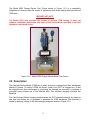
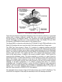
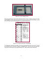
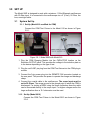
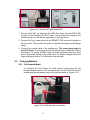
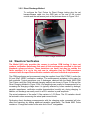
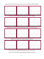
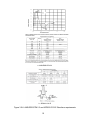
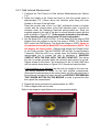
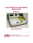
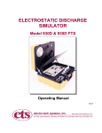
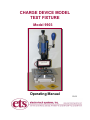
CHARGE DEVICE MODEL
TEST FIXTURE
Model 9903
Operating Manual
10/12
1.0 INTRODUCTION
The rapid advancement in the electronics industry during the past decade has placed an
increasing importance on the understanding of electrostatics and its effect on electronic
devices and systems. Electrostatic discharge (ESD) is a common cause of microelectronic
circuit failure. Many devices can be seriously damaged or destroyed by an electrostatic
discharge below 20 Volts. The sensitivity to ESD of other components has also become
evident through use, testing and failure analysis. The trend in technology towards greater
complexity, increased packaging density and hence thinner dielectrics between active
elements result in parts becoming even more sensitive to ESD.
Failure mechanisms of electrical and electronic parts due to ESD typically include thermal
breakdown, metalization melt and bulk breakdown that are power dependent; dielectric
breakdown, metalization to metalization arc over, surface breakdown and surface inversion
that are voltage dependent.
ESD can also induce latent failure mechanisms in both MOS structures and bipolar
junctions in both discrete devices and microcircuits. This latent failure mechanism results in
performance degradation and eventually a failure.
Personnel are prime sources of ESD for damaging electrical and electronic parts.
Electrostatic charges generated by rubbing or separating materials are readily transmitted
to a person’s conductive sweat layer charging that person. When a person handles or
comes in close proximity to an ESD sensitive part, that part can then be damaged from a
direct discharge by touching the part or by subjecting the part to an electrostatic field.
However, another type of discharge that is far more severe than the discharge from a
person touching a device is the Charge Device Model (CDM). This occurs when the device
itself becomes charged then touches ground a very fast rise time discharge can occur.
Charge
Touch to GND for discharge
GND
Figure 1.0-1: Basic Charge Device Model equivalent circuit
The CDM discharge is a function of the device capacitance that may be as low as a few
picofarads or can be as high as several hundred picofarads. This variation has a significant
affect on the severity of the discharge. Small component packages may not be able to hold
sufficient charge to meet specified discharge levels.
The Charged Device Model (CDM) test, as defined in standards JEDS22-C101C,
ANSI/ESD-STM 5.3 and AEC-Q101-005 describe a test procedure where a component is
slowly charged to a given voltage and then discharged to ground through one of the device
leads. The CDM test permits either field induced or direct charge/discharge.
1
The Model 9903 Charge Device Test Fixture shown in Figure 1.0-1 is a completely
integrated unit that provides the means of performing both direct charge and field induced
CDM tests.
IMPRORTANT NOTE
The Model 9903 only provides the means to perform CDM testing. It does not
produce verification waveforms that meet all the requirements specified in the test
standards referenced above.
Figure 1.0-1: Model 9903 Charge Device Model Test Fixture
2.0 Description
The Charged Device Model (CDM) test is when a device is charged and then discharged
directly to ground. To create a CDM the Device Under Test (DUT) is charged as if it was
the capacitor and then discharged by grounding the desired pin manually by lowering a
grounded spring loaded pin to the desired lead. Two different charging methods are
specified.
The Field Induced Model charging method raises the DUT potential indirectly by induction
and then the desired pin is grounded to generate the CDM discharge. The potential is
raised by applying voltage to the field-charging electrode shown in Figure 2.0-1.
2
Figure 2.0-1: Field Induced Charge Device Model
Tests that are performed using Direct Charging is when the device is placed on a grounded
surface with or without a dielectric isolator and one or more pins are charged directly
through at least a 100 MegOhm resistor. The respective pin is then discharged directly to
ground. Discharge rise times are in the picosecond range. The Models 910 and 9910
incorporate a 400 MegOhm series resistor in the charging circuit.
The Model 9903 in conjunction with either the ETS Model 910 with CDM modification or the
Model 9910 enables the user to perform both Field Induced and Direct Charge tests.
The CDM Test Fixture shown in Figure 1.0-1 consists of a magnetic stainless steel field
induction plate/ground plane and a control module that controls the charging and grounding
function. It contains the upper ground plane, spring-loaded discharge pin and the discharge
button. The internal control electronics time the charge and discharge function of the field
induction plate and DUT. This enables the DUT to be charged and discharged multiple
times at the same polarity. In addition, the module contains a radial 1 Ohm resistor for
measuring the discharge current. The entire assembly is mounted on a press fixture for
performing the test. To select field induction or direct charging a jumper wire connects the
plate to the voltage output connector on the rear of the control module for field induced
charging or to the ground connector that is also located on the rear of the module for direct
charging. In the latter configuration, a 6” (152mm) charging lead with a 5” (127mm)
minigrabber and 15 megOhm resistor to reduce the effects of parasitic cable capacitance
when the test pin is both charged then discharged is connected to the voltage output. In
addition, the 4 and 30pF calibration discs specified in ANSI/ESD-STM-5.3.1 and the 6.8
and 55pF discs specified in JEDS22-C101C are supplied.
The adjustable fixture shown in Figure 2.0-2 holds devices up to 2.5x2.5” (64x64mm). The
fixture itself has magnets to help align the desired pins with the discharge electrode.
3
Figure 2.0-2: DUT Holding Fixture
The spring-loaded pins (Interconnect Devices Series S, Size 3) shown in Figure 2.0-3 are
interchangeable. Three types are provided. They are round tip (J) for pad terminals, cup tip
(G) for DIP style legs, and point tip (B) for very small contact points.
Figure 2.0-3: Spring-loaded pin configurations
To change pins raise the test head to the top by loosening the lever on the rear. This will
give sufficient room to be able to replace or change the pin. Then move the test head back
to a position where the pin tip is approximately 0.25” (6mm) above the pin under test.
4
3.0 SET UP
The Model 9903 is designed to work with a minimum 1 GHz/4Gsample oscilloscope
with 50 Ohm input. It is connected to the oscilloscope via a 2’ (61cm), 50 Ohm, low
loss, semi-rigid cable.
3.1
System Set Up
3.1.1 Set-Up (Model 910 modified for CDM)
Connect the CDM Test Fixture to the Model 910 as shown in Figure
3.0-1.
Figure 3.0-1: Model 9903 with Model 910
1. Plug the CDM Charging Module into the CAPACITOR location on the
Simulator OUTPUT panel. This provides the voltage to the induction plate or
to the device depending on the type of test.
2. Plug the red 0.080” pin plug from the CDM Test fixture into the CDM plug-in
module.
3. Connect the 3-pin power plug into the REMOTE DIN connector located on
the rear panel. This provides the power to operate the charge and discharge
relays.
4. Connect the coaxial cable to the oscilloscope. The scope input must be
set to 50 Ohms. The scope ground is the ground point to which the CDM is
discharged. For testing at 500V using the small verification discs the cable
can be connected directly to the scope input. For higher voltages and/or the
large verification discs a 10:1 attenuator must be used.
3.1.2 Set-Up (Model 9910)
Connect the CDM Test Fixture to the Model 9910 as shown in Figure
3.0-2.
5
Figure 3.0-2: Model 9903 with Model 9910
1. Plug the red 0.080” pin plug from the CDM Test fixture into the CDM 0.080
pin jack on the Simulator OUTPUT panel. This provides the voltage to the
induction plate or to the device depending on the type of test.
2. Connect the 3-pin power plug into the REMOTE DIN connector located on
the rear panel. This provides the power to operate the charge and discharge
relays.
5. Connect the coaxial cable to the oscilloscope. The scope input must be
set to 50 Ohms. The scope ground is the ground point to which the CDM is
discharged. For testing at 500V using the small verification discs the cable
can be connected directly to the scope input. For higher voltages and/or the
large verification discs a 10:1 attenuator must be used.
2.2
Charging Method
2.2.1 Field Induced Model
To configure the Test Fixture for Field Induced testing plug the red
banana-banana cable into the red banana jack on the rear of the control
module and the red banana jack on the plate as shown in Figure 3.0-3.
Figure 3.0-3: Field Induced connections
6
3.2-2 Direct Discharge Method
To configure the Test Fixture for Direct Charge testing plug the red
banana-banana cable into the GND jack on the rear of the control
module and the red banana jack on the plate as shown in Figure 3.0-4.
Figure 3.0-4: Direct Charge connections
6.4 Waveform Verification
The Model 9903 only provides the means to perform CDM testing. It does not
produce verification waveforms that meet all the requirements specified in the test
standards referenced above. These deviations are small, but may be outside the
limits specified. It is up to the end user to determine that the CDM waveforms
measured with the specified verification modules will meet individual requirements.
The CDM waveforms can be measured using the supplied 4 and 30pF STM5.3, and/or the
6.8 and 55pF JEDEC verification modules. The measurement procedure is the same for
both methods. Typical waveforms over 3 discharges obtained with the Model 9903 CDM
Test Fixture using the Field Induced charging method are shown in Figure 3.0-5a and the
Direct Charging method in Figure 3.05b. Low amplitude can usually be compensated for by
increasing the charging voltage since it is typically affected by losses caused by leakage,
parasitic capacitance, verification module characteristics humidity etc. during charging. In
addition, air discharge can easily result in a 20% variation in peak amplitude.
The actual resistance of the radial 1 Ohm resistor is 1.03 Ohms. The 3% variation should
be factored in when measuring the actual peak current levels.
Performing direct discharge measurements with the charging probe connected will also
affect the waveform by adding additional parasitic capacitance. The Model 9903 Probe
contains a 15 megOhm resistor at the wire end of the 5” minigrabber.
7
ESD STM 5.3, 4pf Disc @ 500V
JEDEC JDCS 22-C101E, 6.8pF Disc @ 500V
ESD STM 5.3, 30pF Disc @ 500V
JEDEC JDCS 22-C101E, 55pF Disc @ 500V
Figure 3.0.5a: Typical Field Induce Model verification waveforms
8
Figure 3.0-6 lists the waveform requirements for both the ESDA and JEDEC standards.
ESD STM 5.3, 4pf Disc @ 500V (Touch disc to charge, remove probe, discharge)
JEDEC JDCS 22-C101E, 6.8pF Disc @ 500V (Touch disc to charge, remove probe, discharge)
ESD STM 5.3, 4pf Disc @ 500V (Hold disc to charge then discharge)
JEDEC JDCS 22-C101E, 6.8pF Disc @ 500V (Hold disc to charge then discharge)
Figure 3.0.5a: Typical Direct Charging Method verification waveforms
9
a. ANSI/ESD-STM 5.3
b. JEDS22-C101E
Figure 3.0-6: ANSI/ESD-STM 5.3 and JEDS22-C101E Waveform requirements
10
6.4.1 Field Induced Measurement
1. Configure the Test Fixture for Field Induced Measurements per Section
3.2.1.
2. Adjust the height of the Press test head so that the ground plane is
approximately 0.5” (12mm) above the induction plate using the lever
located on the rear of the test head.
Place the non-disc side of the 4 or 6.8pF verification module in intimate
contact with the metal surface of the field induction plate. It should be
centered under the Discharge Electrode spring-loaded pin. Place the
supplied magnet to the right of the disc to ensure intimate contact with the
plate as shown in Figure 3.0-7. (If the magnet is placed on the left side,
it may interfere with the relays inside the test head module.)
3. Set the Model 910 or 9910 to 500V. (For the Model 910 the plug-in CDM
Adapter limits the voltage to just the low range of 2000V. For the Model
9910, select the CDM function. This limits the voltage to 1000V. Under no
circumstances should the Model 9903 be operated above 2000V. This
will destroy the timing relays.) Depress and release the Charge button
on the Fixture module. The red CHARGE LED will light for approximately
2 seconds. While the LED is on, quickly lower the module enabling the
spring-loaded pin to contact the disc to discharge it. MAINTAIN
CONTACT WITH THE DISC UNTIL THE LED TURNS OFF. This allows
the disc to remain grounded while the induction plate returns to ground.
Repeat at least 2 more times. The waveforms for the 4.0 and 6.8pF discs
will look similar those shown in Figure 3.0-8. Record and save the data.
If this procedure is not followed, the disc will not charge for the next test.
This timing sequence is critical for the field induced measurement.
Subsequent measurements at the same polarity can then be performed. If
the sequence is broken first lower the test head WITHOUT DEPRESSING
THE CHARGE BUTTON ON THE MODULE in order to ground the disc
then repeat the measurement.
4. Repeat the above procedure for measurements at –500V.
5. Other voltage levels can be used.
Refer to the respective specifications for more procedure details.
Figure 3.0-7: Verification module alignment
11
a. 4.0pF Disc
6.8pF Disc
Figure 3.0-8: Typical Induced Charge waveforms for small discs
6.4.2 Direct Charge Measurement
1. Configure the Test Fixture for Direct Charge Measurements per Section
3.2.2.
2. Adjust the height of the Press test head so that the ground plane is
approximately 0.5” (12mm) above the induction plate using the lever
located on the rear of the test head.
Place the non-disc side of the 4 or 6.8pF verification module in intimate
contact with the metal surface of the grounded plate. It should be centered
under the Discharge Electrode spring-loaded pin. Place the supplied
magnet to the right of the disc to ensure intimate contact with the plate as
shown in Figure 3.0-7. (If the magnet is placed on the left side, it may
interfere with the relays inside the test head module.)
3. Set the Model 910 or 9910 to 500V. (For the Model 9910 select the CDM
function.) There are two direct charging methods.
Touch with minigrabber contact: Depress the Charge button on the
Fixture module. While the LED is on, touch the probe to the disc. Then
quickly lower the module enabling the spring-loaded pin to contact the
disc to discharge it. MAINTAIN CONTACT WITH THE DISC for
approximately 1 second. This allows the disc to remain grounded
ensuring total discharge.
Maintain probe contact to the disc: Depress the Charge button on
the Fixture module. While the LED is on, quickly lower the module
enabling the spring-loaded pin to contact the disc to discharge it.
MAINTAIN CONTACT WITH THE DISC for approximately 1 second.
This allows the disc to remain grounded ensuring total discharge. A 15
megOhm resistor in the probe minimizes the parasitic capacitance
effects of the probe.
12
Repeat the measurement at least 2 more times. The waveforms for the
4.0 and 6.8pF discs will look similar those shown in Figure 3.0-9.
Record and save the data.
4. Repeat the above procedure for measurements at –500V.
5. Other voltage levels can be used.
a. Touch and remove
Probe remains connected
Figure 3.0-9: Typical Direct Charge waveforms for 6.8pF discs
6.5 DEVICE TESTING
The recommended stress levels are slightly different between the JEDEC and
ANSI/ESD specifications as listed in the table below.
Level
1
2
3
4
5
6
JESD Level V
100
200
500
1000
2000
-
ANSI/ESD Level V
125
250
500
1000
1500
2000
6.5.1 Test Procedure
1. Place the DUT either in the holding fixture or directly onto the plate. For
metal encased devices, a 2 mil dielectric may have to be placed on the
plate.
2. Align the spring-loaded pin to the DUT pin to be discharged as shown in
Figure 6.5-1.
3. Lower the module to both verify the alignment and to initially ground the
pin. Do Not Push the Discharge Button.
4. If not already set then set the voltage to the desired level.
13
5. For Field Induce charging, depress the Discharge button momentarily,
then quickly lower the test head enabling the spring-loaded pin to
discharge the DUT. The discharge waveform will be displayed on the
scope. Continue to hold the lever down until the red LED indicator
goes out.
6. For Direct Charging, either touch the minigrabber probe to the desired
pin or connect it to the pin.
Touch with minigrabber contact: Depress the Charge button on the
Fixture module. While the LED is on, touch the probe to the disc. Then
quickly lower the module enabling the spring-loaded pin to contact the
disc to discharge it. MAINTAIN CONTACT WITH THE DISC for
approximately 1 second. This allows the disc to remain grounded
ensuring total discharge.
Maintain probe contact to the disc: Depress the Charge button on
the Fixture module. While the LED is on, quickly lower the module
enabling the spring-loaded pin to contact the disc to discharge it.
MAINTAIN CONTACT WITH THE DISC for approximately 1 second.
This allows the disc to remain grounded ensuring total discharge. A 15
megOhm resistor in the probe minimizes the parasitic capacitance
effects of the probe.
7. For each component, apply 3 positive and 3 negative discharges to each
pin. Observe the discharge on the oscilloscope. Allow at least several
seconds between charge/discharge cycles.
Figure 6.5-1: DUT/Discharge pin alignment
10/12
14
7.0 WARRANTY
Electro-Tech Systems, Inc. warrants its equipment, accessories and parts of its
manufacture to be and remain free from defects in material and workmanship for a period
of one (1) year from date of invoice. It will, at it’s discretion, either replace or repair without
charge, F.O.B. Glenside, similar equipment or a similar part to replace any equipment or
part of its manufacture which, within the above stated time, is proved to have been
defective at the time it was sold. All equipment claimed defective must be returned properly
identified to the Seller (or presented to one of its agents for inspection). This warranty only
applies to equipment operated in accordance with Seller's operating instructions.
Seller's warranty with respect to those parts of the equipment that are purchased from other
manufacturers shall be subject only to that manufacturer's warranty.
The Seller's liability hereunder is expressly limited to repairing or replacing any parts of the
equipment manufactured by the manufacturer and found to have been defective. The Seller
shall not be liable for damage resulting or claimed to result from any cause whatsoever.
This warranty becomes null and void should the equipment, or any part thereof, be abused
or modified by the customer of if used in any application other than that for which it was
intended. This warranty to replace or repair is the only warranty, either expressed or
implied or provided by law, and is in lieu of all other warranties. Seller denies any other
promise, guarantee, or warranty with respect to the equipment or accessories and, in
particular, as to its or their suitability for the purposes of the buyer or its or their
performance, either quantitatively or qualitatively or as to the products that it may produce
The buyer is expected to expressly waive rights to any warranty other than that stated
herein.
ETS must be notified before any equipment is returned for repair. ETS will issue an RMA
(Return Material Authorization) number for return of equipment.
Equipment should be shipped prepaid and insured in the original packaging. If the original
packaging is not available, the equipment must be packed in a sufficiently large box (or
boxes if applicable) of double wall construction with substantial packing around all sides.
The RMA number, description of the problem along with the contact name and telephone
number must be included in formal paperwork and enclosed with the instrument. Round
trip freight and related charges are the owner’s responsibility.
WARNING:
WOODEN CRATES MUST NOT BE USED TO PACKAGE THE ELECTRONIC UNITS.
PACKAGING OF DELICATE INSTRUMENTS IN WOODEN CRATES SUBSTANTIALLY
INCREASES THE CONTENT’S SUSCEPTIBILITY TO SHOCK DAMAGE. ELECTROTECH SYSTEMS, INC. WILL NOT ASSUME RESPONSIBILITY FOR ADDITIONAL
COST OF REPAIR DUE TO DAMAGE INCURRED DURING SHIPMENT DUE TO POOR
PACKAGING.
15