1
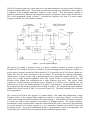
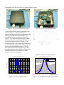
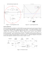
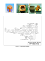
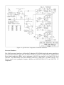
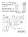
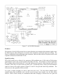
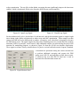
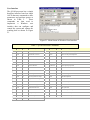
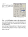
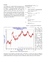
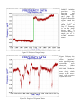
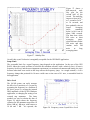
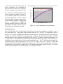
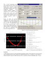
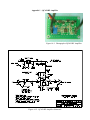
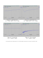
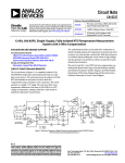
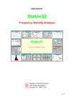
The Quartz Crystal Anomaly Detector (QCAD) System W.J. Riley Hamilton Technical Services Beaufort, SC 29907 USA [email protected] Keywords Quartz crystal resonator, frequency jumps, crystal anomalies, drive level sensitivity, temperaturefrequency characteristic, crystal resistance. Abstract This paper describes a Quartz Crystal Anomaly Detector (QCAD) system for detecting jumps and other anomalies in quartz crystal resonators. The crystal under test is operated at its minimum impedance frequency in a shunt network excited by a FM modulated, DDS synthesized RF source. The resulting AM signal is detected and used in a frequency lock loop servo to lock the frequency of the RF source to the crystal resonance. The DDS tuning word is a direct measure of the crystal frequency, and the DDS amplitude sets the crystal drive level. Relatively fast (<1 second), low noise (pp1011), and high resolution (pp1014) frequency measurements are supported by the associated embedded software and user interface, and the crystal behavior can be observed as a function of time, temperature, drive level and other variables in a convenient and inexpensive way. Introduction The Quartz Crystal Anomaly Detector (QCAD) is a measuring system for detecting frequency jumps and other anomalies, and characterizing the general behavior, aging, temperature coefficient and drive level dependence of quartz crystal resonators. The QCAD system was developed as a means to screen ≈13.4 MHz AT-cut fundamental mode quartz crystal resonators for anomalous frequency jumps in critical GPS rubidium atomic clock application [1]. While crystal oscillator static frequency error is removed by the atomic clock’s frequency lock loop, a crystal frequency jump can cause a permanent phase (time) error as the loop corrects a relatively large (> pp109) frequency change. The mechanisms behind such quartz crystal resonator frequency jumps are complex, and beyond the scope of this paper. But it is well known that they depend on both the individual device and its operating conditions (in particular, temperature and drive level). It is therefore necessary to test every resonator over a fairly long period of time (e.g., 1 month) under its actual operating conditions to avoid anomalous behavior. Furthermore, it is more effective to perform that screening prior to installing it into flight hardware. The equivalent circuit parameters for these crystals are shown in Table 1. Table 1. Parameter L1 C1 R1 C0 Equivalent Circuit Parameters of 13.401344 MHz Crystal in PerkinElmer GPS RAFS Units Value Remarks mH 35 Nominal value pF 0.004030346 Value so that the crystal is resonant with its specified 25 pF load capacitance at nominal 13.401344 MHz 30 Maximum value pF 1.2 Nominal value The QCAD system operates the crystal under test as the shunt element in a two port network excited by a frequency modulated RF source. The network transmission is sensed by an AM detector whose output is a minimum at the minimum impedance frequency of the crystal. That discriminator response is amplified, synchronously detected, and integrated to produce a frequency control voltage for the source. The overall arrangement, shown in Figure 1, resembles the frequency lock loop of a passive atomic frequency standard. No test oscillator is required. Figure 1. QCAD System Concept This process of locking a frequency source to a passive resonance response is similar to that first described by R.V Pound for microwave oscillator [2], and an arrangement for locking an oscillator to a passive quartz resonator described by Walls and Stein [12]. In particular, the QCAD system is based on a similar one that the author developed in the late-1960’s for measuring the frequency-temperature characteristics of quartz crystals used in uncompensated room temperature counter time bases. That system used a single frequency-modulated source that excited a bank of crystal networks and AM detectors whose outputs were multiplexed into a single frequency lock servo. That system, which required an external frequency measuring system, operated at a relatively slow sampling rate, but performed very well for its intended purpose for crystal TC measurements. An important advantage of the arrangement is that no phase-sensitive RF switching is required. The calculated and actual resonance characteristics for the crystal of Table 1 are shown in Figures 4-6. The actual resonance plot is inverted by the preamplifier. The current QCAD system also operates in a similar fashion. But, rather than multiplexing a single frequency source, it uses separate DDS synthesizers clocked by a frequency reference to excite each crystal, whose tuning words directly indicate the crystal frequency. That parallel architecture can operate at a faster rate and is easily expanded to the number of channels required. No external frequency measurement system is needed, and it retains the feature that the RF phase is not critical, thus permitting the crystal network to be located remotely (e.g., in a temperature chamber) from the RF source and processing circuits. The present embodiment includes a programmable crystal oven temperature and crystal drive power, both of which are important factors related to frequency jumps. Photographs of the QCAD system are shown in Figures 2 and 3. Figure 2. QCAD System Exterior of Box Figure 3. QCAD System Interior of Box A circuit model of the QCAD crystal network is shown in Figure 4. The QCAD Windows applications includes means for sweeping the DDS frequency through the crystal resonance and recording the detector response, as shown in Figure 5. It is somewhat asymmetrical, perhaps because of the finite sweep speed. The data can be replotted and fitted as shown in Figure 6. The Lorentizian fit has a full width at half amplitude of 287 Hz and inflection points at ±83 Hz (nearly the same as the normal FM deviation of ±100 Hz). The single-tuned circuit fit implies a Q=98,000, the typical specified value. Neither fit follows the resonance data at lower amplitudes, probably because of detector nonlinearity. Figure 4. Model of Crystal Resonance QCAD Frequency Sweep for Bliley Crystal S/N 040 QCAD Frequency Sweep for Bliley Crystal S/N 040 1.5 1.5 1.0 Detector Voltage, VDC Detector Voltage, VDC QCAD Sweep Data Lorentzian Line Fit Single-Tuned Circuit Fit 0.5 0 13.3995 13.4000 13.4005 13.4010 Frequency, MHz Figure 5. Actual Crystal Resonance 13.4015 1.0 Lorentizian Fit: Center frequency=354 Hz FWHA=287 Hz Peak=1.45 Single-Tuned Circuit Fit: Center Frequency=352 Hz Q=98,000 Peak=1.54 0.5 0 -200 -100 0 100 Lorentzian Fit: y=b/(1+(4*(x-c)*(x-c)/(a*a))) a=286.715, b=1.45403, c=354.095 200 300 400 500 600 Frequency, Hz wrt 13.4 MHz 700 800 900 1000 Single-Tuned Circuit Fit: y=a/sqrt(1+(2*b*(x-c)/c)*(2*b*(x-c)/c)) a=1.53634, b=2.57402, c=352.215 Figure 6. Crystal Resonance Replotted and Fitted Block Diagram The single channel QCAD system is implemented on two 3.8” x 2.5” circuit boards, as shown in the block diagram of Figure 7. The detector board comprises the crystal and crystal network, its oven, oven temperature controller and set-point DAC, and the AM detector, preamplifier and ADC. The processor board contains the DDS RF source, the signal processor, and the RS-232 PC interface. Figure 7. QCAD System Block Diagram Minimum Impedance Frequency The QCAD system tunes the DDS to the minimum impedance frequency of the crystal under test. That frequency, fm, is slightly below the series resonant frequency, fs, as shown in the impedance circle of Figure 10 and impedance plot of Figure 9 [3-6]. For the ≈ 13.4 MHz crystals described in Table 1, the minimum impedance frequency is lower than the series resonant frequency by about 2.1x10⁻⁸. The QCAD system is not particularly concerned with the absolute crystal frequency but rather its stability. C0 f m f s 1 2 2 C Q 1 Figure 9. Crystal Impedance Circle Figure 10. Crystal Impedance Plot Detector Hardware The QCAD detector board holds the 6 dB 50 RF drive input attenuator and crystal network, followed by a forward biased temperature compensated diode AM detector, a x25 signal preamplifier and the Analog Devices AD7457 12-bit analog-to digital converter (ADC). It also has the oven temperature controller with its thermistor bridge, DC amplifier, voltage-to-current converters, heater transistors, demand current limiter, and an Analog Devices AD5320 12-bit digital-to-analog converter (DAC) to set the oven temperature. Those circuits are shown in Figure 11. The oven uses four thermistors and heaters on each side to minimize thermal gradients, as shown in Figure 12. Schematic diagrams of the QCAD detector and temperature controller circuits are shown in Figure 13 and 14. Figure 11. Detector Circuits Figure 12. Crystal Oven Figure 13. QCAD Detector Schematic Figure 14. QCAD Oven Temperature Controller Schematic Processor Hardware The QCAD processor board uses a Microchip Technology PIC16F648A single-chip micro-controller to process the discriminator signal from the detector board, to control an Analog Devices AD9852 48-bit direct digital synthesizer (DDS), and to implement an RS-232 user interface via a MAX3235E level converter. The DDS and PIC are both externally clocked at 20 MHz from a 10 MHz reference via a discrete tuned circuit push-push frequency doubler and MC100LVEL16 ECL and LMV7219 5V comparators. The processor operates at 5 volts, the DDS at 3.3 volts, and a 74LCV244A logic level converter is used between them. The microprocessor flash program memory can be reprogrammed via an incircuit programming connector. The DDS uses an internal x6 clock multiplier, and is followed by a 7pole 15 MHz elliptic LPF. The DDS spectrum is quite clean, having no visible spurious components except for some -72 dBc noise around the carrier, as shown in Figure 15. The QCAD processor also has a 12-bit DAC that is used to produce an analog output to drive a stripchart recorder. Schematics of the QCAD processor and DDS circuits are shown in Figures 16 and 17. Figure 15. DDS Spectrum Figure 16. QCAD Processor Schematic Figure 17. QCAD DDS Schematic Firmware The firmware of the QCAD processor has two main functions, processing the discriminator signal to tune the DDS frequency and realizing the user interface that controls the system and outputs its readings. The former is implemented using multi-phase timer interrupts, while the latter utilizes a loop that waits for and responds to characters from the RS-232 I/O. Signal Processing The QCAD system uses a relatively low squarewave FM modulation rate (19 Hz) and an FM deviation approximately equal to the crystal resonance linewidth (±100 Hz). This produces a detected signal that has switching transient followed by DC levels that indicates the frequency offset from the center of the resonance, where they are equal for the two half cycles. Oscilloscope traces of the QCAD discriminator signal are shown in the upper portion of Figures 18 and 19 for open and closed loop conditions. The lower traces are the squarewave FM waveform. Two types of signal averaging are used to reduce the noise level. The first utilizes multiple signal samples during each modulation cycle, and the second averages those samples over the data stream interval. Both of those actually use summation rather than averaging to increase the servo gain and reduce quantization. The net effect is that further averaging does not significantly improve the short-term stability, which is dominantly flicker noise from the diode detector and preamplifier. Figure 18. Open-Loop Signal Figure 19. Closed-Loop Signal Each modulation half cycle is divided into 16 sub-intervals, and the discriminator signal is sampled eight times during eight of those sub-intervals to reduce noise and ADC quantization. Those samples are then summed and the half cycles differenced to produce a frequency error value that is integrated to become the DDS tuning word. The signal samples are taken after a blanking interval to exclude the FM switching transients (which, in principle, would cancel) while additional samples are taken during the peak of the transient for monitoring purposes, as shown in Figure 20 from the QCAD user interface application. These signal waveforms closely resemble those of a passive cesium beam tube atomic frequency standard. Calculations are performed during the various sub-intervals to perform additional averaging and prepare the DDS tuning word, RS-232 and stripchart recorder data streams. A relatively fast (115,200) RS-232 baud rate is used to maximize the allowable data stream rate. Figure 20. Signal Monitor Panel User Interface The QCAD processor has a simple hardware interface based on single ASCII character commands to enter parameters and perform queries as shown in Table 2. These commands are then used to implement a Windows user interface that can configure and control the system and capture the resulting data as shown in Figure 21. Figure 21. Main Screen of Windows User Interface Table 2. QCAD Processor Commands Cmd Type # Bytes Description Cmd Type # Bytes Description 0 Command 1 Reset PIC processor I Write 2 Enter temporary DAC setting 1 Read 1 Get PIC S/W revision # K Write 2 Enter oven set point temperature 2 Read 4 Get HF DDS sub-word L Write 4 Enter LF DDS sub-word 3 Read 4 Get LF DDS sub-word M Write 2 Enter modulation rate 4 Read 2 Get modulation rate N Command 1 Tune down or set DAC to 0 5 Read 1 Get DAC MS bit # O Command 1 Select open loop operation 6 Read 3 Get DAC word P Read 1 Get servo state 7 Read 1 Get PC data stream rate R Write 1 Enter PC data stream rate 8 Read 1 Get servo gain S Command 1 Save all settings in EEPROM 9 Read 2 Get average detector voltage T Read 2 Get DDS amplitude A Read 2 Get peak detector voltage U Command 1 Tune up or set DAC to FS B Write 1 Set DAC MS bit # V Write 2 Enter DDS amplitude C Command 1 Select closed loop operation W Write 1 Set EEPROM state D Read 2 Get discriminator error # Read 1 Get system S/N E Read 1 Get EEPROM state $ Read 1 Get oven set point temperature F Write 1 Enter QCAD system S/N < Command 1 Disable timer interrupts G Write 1 Enter servo gain > Command 1 Enable timer interrupts H Write 4 Enter HF DDS sub-word Configuration The QCAD Windows user interface includes a Configuration screen (shown in Figure 22) that can be used to display and change set all of the system’s operating parameters. Please consult the Help file for the details about using the QCAD configuration screen. Figure 22. QCAD Configuration Screen Performance The performance of the QCAD system has met its requirements and exceeded its expectations. In particular, the noise level and corresponding short and medium term stability is much better than needed to detect significant frequency jumps for the GPS RAFS application. The temperature and drive level sensitivity of the crystal are even larger and are even more easily resolved. As expected, the most critical aspect is crystal temperature stability, which requires good oven temperature control, especially if the measurements are made at a fixed temperature rather than close to the crystal turnover point. Little variation has been seen in the level of short term instability between different crystals, but the system could certainly detect a noisy device. Although the DC level of the AM detector provides information about the crystal resistance, no attempt has been made to quantify that parameter with this system. At a minimum, doing so would require compensating for the RF drive level and diode detector temperature dependence. Network analyzer and bridge methods are better suited for that purpose. The objective here was to detect and quantify frequency jumps as a function of time, temperature and drive level. If, as is likely, there is a corresponding resistance change, it doesn’t really matter because an anomaly has occurred and its severity is judged by the size of the frequency change. Example An example of a 1-month QCAD measurement run is shown in the figures below. This run resulted in about 2.6 million ≈ 1 second data points. Figure 23 shows the system configuration for this run, which was conducted between 08/05/2009 and 09/05/2009 on Bliley Crystal S/N 040 at its upper turnover temperature of 51ºC and maximum drive power of about -8 dBm. The absolute frequency at fm, the crystal’s minimum impedance point, is the average to the two DDS words, 13.400342325 MHz, about 1.002 kHz below its nominal operating value in the RAFS. QCAD #1 Configuration S/W Rev = 0.22 UTC: 2009-09-05 13:03:14 MJD: 55079.543912 Crystal S/N: B040 50C 0dB Oven Temperature: Setpoint: 0347 = 50.99 Deg C DDS: HF Word: 1C966DA0D16F = 13.400442325084470 MHz LF Word: 1C9651AA8A0E = 13.400242325084548 MHz Deviation: 1BF64761 = 200.0000 Hz Amplitude: Maximum Data Stream: Stream Rate: 13 Tau: 0.9961 sec Frequency: 6DA0D1 = 5.851635e-05 Servo: Mod Rate: E000 = 19.0735 Hz Gain: 08 = x 256 Loop = Closed EEPROM: Read = No Detector: Voltage: 6948 = 1.028 VDC Signal: 8718 = 28.3 % Error: 0001 Status = Green (Closed Loop, Small Error, OK Signal) DAC: MS Bit #: 18 = 24 Reading: 66B = 0.401 VDC Figure 23. QCAD System Configuration The entire frequency record is shown in Figure 24 after averaging the data by a factor of ten and removing twelve gross outliers caused by power line disturbances during thunderstorms [7]. Several frequency jumps are apparent, as is some cycling and wandering, but there is little overall drift. The crystal was operated near its 50ºC turnover point at a drive level of about 160 uW. Figure 24. Overall 1-Month Frequency Record Zooming in on the frequency record shows only a small effect (≈ 1x10⁻¹⁰ p-p) from air conditioner temperature cycling with a period of about 40 minutes. The cause of the slower semidiurnal cycling is probably thermal, but its exact origin has not been established, and may follow power line variations. Stable32 includes provisions for detecting and analyzing frequency jumps [8]. Figure 25 shows the region around the largest jump of about 3.1x10⁻⁹ at Day 5.7. Zooming in on the jump shows that it occurred during a single pair of 1second measurements. Figure 25. Region of Largest Jump Figure 26 shows the region around day # where “popcorn” noise type frequ-ency excursions were observed. Other crystals have shown this kind of behavior more clearly, which seems to be associated with excessive crystal drive level. Figure 26. Region of “Popcorn” Noise Figure 27 shows a drift-removed stability plot for the second half of the record. The stab-ility improves from 6x10-11 at 1 second to 2x10-11 at 30 seconds, and then gradually rises at longer averaging times, remaining below 1x10⁻¹⁰ out to about 2000 seconds. The data show white FM noise at short averaging times, which becomes flicker FM noise and then random walk FM noise at long averaging times. Figure 27. Stability Plot Overall, this crystal’s behavior is marginally acceptable for the GPS RAFS application. Jump Limit The acceptable limit for a crystal frequency jump depends on the application. In the case of the GPS RAFS, where the crystal oscillator is locked to the rubidium reference with a relatively fast (<10 msec) frequency lock loop, and the most important requirement is to maintain sub-nanosecond timing, the issue becomes what time error results as the loop corrects the frequency jump. As a rough estimate, a 1x10⁻⁸ frequency change that persisted for 10 msec would cause a time error of 0.1 nsec, a reasonable limit for this application. Drive Level The QCAD system can easily measure the drive level sensitivity of a crystal by measuring the frequency as a function of RF drive power by varying the internal DDS amplitude via the QCAD Windows application, or changing the setting of an external step attenuator. The latter method was used to obtain the data of Figure 28, which shows the frequency variation for RF attenuator steps from 10 dB to 0 dB in 1 dB steps, with retraces to 10 db and 7 dB. As expected, the Figure 28. Frequency versus Crystal Drive Level The variation in crystal dissipation versus crystal resistance is shown in Figure 29 for a nominal 0 dBm drive level to the QCAD detector board. That level can be reduced by DDS attenuator setting in the QCAD Windows interface Configuration screen, or increased by adding an optional amplifier between the DDS O/P and detector RF input connectors on the QCAD Processor and Detector boards. QCAD Crystal Dissipation Versus Crystal Resistance for 0 dBm Detector Board Drive 0.16 0.15 2 1 y = -1.057E-4x +0.007248x +0.02740 Crystal Dissipation, mW sensitivity increases with increasing drive power, estimated to be a maximum of 500 microwatts in these tests where the RF drive sensitivity was about 2x10⁻⁷/dB. 0.14 0.13 0.12 0.11 0.10 0.09 0.08 10 15 20 25 30 Crystal Resistance, Ohms Figure 29. Crystal Dissipation Versus Resistance Temperature Scan The QCAD Windows user interface application includes provisions for performing a temperature scan on the crystal under test. Temperature scans anywhere between 25ºC and 65ºC are supported in steps of about 10 mºC with an adjustable initial dwell time and ramp rate. Temperature and averaged frequency readings are written to a disk file at each temperature increment. The resulting temperature coefficient data are fitted to a cubic equation, and estimates of the crystal TC parameters, turnover temperatures, ATcut angle and TC at the nominal 45 ºC RAFS operating temperature are provided. These estimates are satisfactory even when based on a fairly narrow temperature scan. The TC and fit data are plotted onscreen, the former as the scan progresses. A 30ºC to 65 ºC scan at a rate of 2 ºC takes 17½ hours and produces about 3500 data points, where each frequency value is the result of averaging about 18 1-second measurements, as shown in the example below. The ambient temperature must be at least 5-10 ºC below the lowest scan temperature to maintain proper oven temperature control. The ≈ 10 mºC temperature steps cause transients in the crystal oven heater power, but they are brief (lasting only a couple of seconds) and within the dynamic range of the temperature controller. The resulting frequency changes are integrated by the relatively large thermal mass of the oven, and become cyclic fluctuations on the order of 2x10⁻¹⁰ so that even the unaveraged frequency record is smooth. Figure 30 shows the QCAD temperature scan screen after the completion of a scan with resulting red TC data and superimposed green cubic fit. A EasyPlot plot of the TC data is shown in Figure 31, and an excerpt from the data file is shown in Figure 32, which includes the cubic fit coefficients and derived crystal parameters [9]. Figure 30. QCAD Temperature Scan Screen PerkinElmer QCAD System TC Data for Crystal S/N Bliley 040 2.5 Frequency, pp10 6 2.0 1.5 1.0 0.5 0 30 40 50 60 Temperaure,ºC Figure 31. Crystal TC Plot with EasyPlot 70 Crystal S/N: Bliley 040 Start Temperature: 30.00 End Temperature: 65.00 Scan Rate: 2.00 Tau: 9.961472e-01 30.00 2.044269e-06 1.009 ... 64.98 2.392494e-06 1.010 Plot crystal TC cubic fit coefficients df/f = ao+a1*t+a2*t^2+a3*t^3 a0: 7.164359e-07 a1: 3.042312e-07 a2: -1.252024e-08 a3: 1.265733e-10 Standard crystal TC cubic fit coefficients df/f = A1(T-To)+A2(T-To)^2+A3(T-To)^3 To = 26.4 deg C A1: -9.218778e-08 A2: -2.495631e-09 A3: 1.265733e-10 Delta Theta: 1.090 min of arc wrt nominal angle of 35.25 degrees Upper turn point: 49.88 deg C Lower turn point: 16.06 deg C TC slope at 45 deg C: -5.37e-08 per deg C Figure 32. Excerpt from scan.frd Data File Scan Rate A bidirectional scan may be used to determine the optimum scan rate, which should be as fast as possible while avoiding hysteresis, and to minimize the initial temperature lag. An example of a fast scan rate is shown in Figures 33 and 34, which used a rate of 20 ºC per hour, x10 the recommended value. Even at that high rate the cubic fit determined by the average of the two directions is reasonably accurate. For example, the upper turnover temperature is estimated as 49.97 ºC instead of 49.88 ºC. PerkinElmer QCAD System TC Data for Crystal S/N Bliley 040 2.0 Relative Frequency, pp10 6 1.5 1.0 0.5 0 -0.5 30 40 50 60 70 Temperaure,ºC Figure 33. 20 ºC/Hour Scan Setup Figure 34. Scan Results at 20 ºC/Hour Crystal Resistance The detector voltage at the center of the resonance provides information about the crystal resistance, as shown in Figure 35 for crystal resistance values of 10, 20 and 30 ohms. It is therefore be possible to estimate the minimum impedance resistance of the resonator by detector voltage measurements made at the resonance center with normal RF level and off resonance at a reduced RF level that produces the same detector voltage. The crystal resistance estimate is given by: W2 Figure 35. Crystal Resonance vs. Resistance Characteristic Rx 72 W1 W 2 where 72 ohms is the RF source impedance seen by the shunt crystal, W1 is the normal RF amplitude word, and W2 is the off-resonance reduced RF amplitude word. This resistance estimate is independent of the actual detector and preamplifier transfer functions, detector bias, or temperature. Rx estimates of about 16 ohms were obtained for the Bliley 040 over a 30ºC to 65º range, a value that implies Q=184,000. Network Analyzer Measurements The validity of the crystal resistance measurement was confirmed with reflection coefficient measurements made on a vector RF network analyzer (VNA) [10] as shown in Figure 36. The plot shows the magnitude of the crystal impedance and the reflection coefficient (Smith chart) near the crystal resonant frequency. The marker at the minimum |Z| point shows a resistance of 15.4 ohms, in good agreement with the QCAD value of 16 ohms. Figure 37 shows the crystal equivalent circuit parameters extracted by the same instrument by fitting the measured impedance circle. The measured motional inductance value is in good agreement with that shown in Table 1. Figure 36. VNA Crystal Impedance Measurement Figure 37. Measured Crystal Equivalent Circuit Parameters Alternative Crystal Networks A resistive reflection coefficient bridge could be used in place of the shunt crystal network, with the crystal in the unknown bridge arm [11]. The resistance of the other equal bridge arms would have to close to that of the crystal resonance resistance to obtain a good null condition, and a balun transformer would be required at the output to the detector. The response of the reflection coefficient bridge would have essentially the same FWHA and require higher source power for the same crystal drive, and it is not obvious that that arrangement would offer any advantage over the shunt network. Other Applications While the present embodiment of the QCAD system is directed specifically to measuring ≈ 13.4 MHz AT-cut fundamental mode resonators, the DDS synthesizer and its associated firmware can be rather easily adapted for other frequencies in this general range. Similarly, the FM modulation rate and deviation can be adjusted for other resonator types. The physical arrangement of a single unit for each crystal under test could be changed to a multichannel architecture with a single RF source and processor by switching the detector signals as was done in the original 1960’s system. The on-board crystal oven could be replaced by an external temperature chamber, perhaps for multiple crystals under test. The emphasis could be changed from observing the behavior of a device under constant operating conditions to making TC measurements (or even characterizing static g sensitivity or radiation sensitivity). As presently implemented, it is easy to sweep the crystal resonance or scan the unit versus temperature to find its turnover point. Specifications The specifications for the QCAD system are shown in Table 3. Table 3. Quartz Crystal Anomaly Detector (QCAD) System Specifications Parameter Frequency Range Frequency Lock Frequency Resolution DDS Output Power Quartz Crystal Compatibility Quartz Crystal Oven Temperature Crystal Drive Power Range Measurement Interval Modulation Rate Short Term Stability Temperature Coefficient Strip Chart Recorder Output Frequency Reference Signal Monitor Oscilloscope Sync Power Supplies (12V @ 1.5A and 3.3V@ 4.0A with 5.5 mm OD connectors supplied with unit) Size (LxWxH) Weight Inputs Outputs Interfaces Internal Firmware User Interface Software Analysis and Plotting Software Specification 13.399658203125 To 13.401489257812 MHz (-55.4 to +81.3 ppm wrt nominal 13.400400 MHz At minimum impedance frequency of quartz crystal resonator under test 48-Bit internal DDS, LSB ≈ 5.03x10⁻¹³, 3-Byte (24 bits) numeric data stream with 137 ppm range and 8.14x10⁻¹² resolution 0 dBm nominal (max), adjustable with 12-bit resolution HC-37/U-1 (TO-8) Holder, 5 0.017” diameter leads on 0.1” grid, 0.2” to 0.6” long +25ºC to +65ºC, settable with ≈ 0.02 ºC resolution -8 dBm nominal (max), adjustable with 12-bit resolution Adjustable between ≈ 1 to 13 seconds (shorter intervals possible but not recommended) 19 Hz nominal (can be adjusted, but not recommended) ADEV < 1x10⁻¹⁰ at 1 second (2x10-11 typ at=30 sec) TC < 2x10⁻⁹/ ºC 0 to +1 VDC, 12-bit resolution with range adjustable in octave steps from 5.03x10⁻¹³ to 1.71x10⁻⁵ FS, update rate same as modulation rate (w/o ext analog LPF) 10 MHz , +7 dBm nominal (0 to +10 dBm) 0 to +2.5 VDC, shows DC detector bias (1.0 VDC nominal) and recovered discriminator signal +5 V squarewave at modulation rate +12 VDC @ 300 mA max (2.5 mm inner conductor) +3.3 DVC @ 350 mA (2.1 mm inner conductor) 3 W SS at 25ºC and 45ºC setpoint from 120V AC line 7.01” x 7.01” x 2.64” (Hammond 1590F Enclosure) 2.8 pounds DC Power, Frequency Reference (BNC) Strip Chart Recorder (dual binding posts), Signal Monitor (BNC), Oscilloscope Sync (BNC), Crystal Oven Heater Voltage Monitor (2 banana jacks) RS-232, bipolar, 115,000 Baud, 8 data bits, 1 stop bit, no parity (USB with adaptor) ASCII character command interface. Can be updated via incircuit programming QCAD Windows application provides parameter setting, data monitoring and capture, frequency and temperature sweeps (supplied with unit) Stable32 (supplied with unit), EasyPlot (recommended) Analysis Software The Stable32 program for frequency stability analysis can be launched by a button on the QCAD Windows user interface at any time during a run. Besides its general capabilities, Stable32 includes several features of particular interest for use with the QCAD system. An automation script may be invoked when the program is launched to automatically perform an analysis. During manual file reading, the Comments button of the Multicolumn Data Details function can be used to display comments that are automatically or manually entered into the QCAD data file during a run. Stable32 also includes a frequency jump detection and analysis feature that can be used to check the record for jumps. EasyPlot or another general-purpose scientific plotting program can be used to plot the results of QCAD frequency sweeps and temperature scans from their respective data files. Conclusions A simple yet effective method has been developed for making frequency measurements on quartz crystal resonators that is well suited for evaluating their general behavior, aging, frequency jumps, temperature coefficient, drive level sensitivity and the like. The QCAD system concept has been found effective for screening resonators for frequency jumps and other anomalies, and it could be adapted for a variety of measurements on quartz crystal resonators. Acknowledgements The author wishes to acknowledge the support of the PerkinElmer Rubidium Department for the development of the QCAD system. References 1. GPS Rubidium Atomic Frequency Standard (RAFS), PerkinElmer, Inc., Salem, MA 01970 USA. 2. R.V. Pound, "Electronic Frequency Stabilization of Microwave Oscillators", Review of Scientific Instruments, Vol. 17, pp. 490-505, November 1946. 3. J.R. Vig, Quartz Crystal Resonators and Oscillators for Frequency Control and Timing Applications A Tutorial. 4. E. Hafner, “The Role of Crystal Parameters in Circuit Design”, Proceedings of the 22nd Annual Frequency Control Symposium, April 1968, pp. 269-281. 5. W.S. Metcalf, “Practical Crystal Measurements and Standardization”, Proceedings of the 27th Annual Frequency Control Symposium, June 1973, pp. 55-62. 6. V.E. Bottom, Introduction to Quartz Crystal Unit Design, Van Nostrand Reinhold, 1982, ISBN 0442-26201—9. 7. User Manual, Stable32 Program for Frequency Stability Analysis, Hamilton Technical Services, Beaufort, SC 29907 USA. 8. W.J. Riley, "Algorithms for Frequency Jump Detection", Metrologia 45 (2008) S154-S161. 9. EasyPlot Program for Scientific Plotting and Data Analysis, Spiral Software, Brookline, MA 02146 USA. 10. T. Baier, DG8SAQ Vector Network Analyzer. 11. R.C. Smythe, “An Automated Resonator Measurement System Using a Reflection Coefficient Bridge”, Proceedings of the 35th Annual Frequency Control Symposium, May 1981, pp. 280-285. 12. F.L. Walls and S.R. Stein, “A Frequency-Lock System for Improved Quartz Crystal Oscillator Performance”, IEEE Transactions on Instrumentation and Measurement, Vol. IM-27, No. 3, September 1978, pp. 249-252. Appendix 1 – QCAD RF Amplifier Figure A1-1. Photograph of QCAD RF Amplifier Figure A1-2. QCAD RF Amplifier Schematic Figure A1-3. Input Return Loss S11 = -37 dB, VSWR = 1.03 at 13.4 MHz Figure A1-4. Output Return Loss S22 = -48dB, VSWR = 1.01 at 13.4 MHz Figure A1-5. Forward Gain S21 = 12.2 dB at 13.4 MHz Figure A1-6. Reverse Isolation S12 = -70 dB at 13.4 MHz File: The Quartz Crystal Anomaly Detector.doc, W.J. Riley, Hamilton Technical Services, Revision D, December 23, 2009