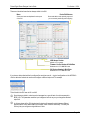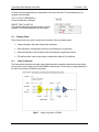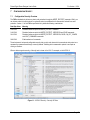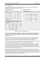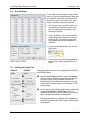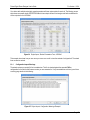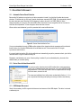
1
Fusion Digital Power Designer User’s Guide
For Version 1.3.23 or Higher · User’s Guide Last Updated on 15 September 2007
Documentation for the Microsoft WindowsTM application used to monitor and configure Texas
Instruments UCD91XX and UCD92XX PMBusTM digital power controllers.
This user’s guide will be updated in 2010 to
document changes and new features in Fusion
Digital Power Designer.
This version of the user manual has been updated to
reflect the equations used to calculate the loop
response in GUI versions 1.5.41+. See section
8.11.1 (UCD91XX) or 8.12.1 (UCD92XX).
Version 1.6+ of the GUI fully supports monitoring
and configuring multiple devices in online mode (this
document says the GUI can only configure a single
device). In offline mode, however, the GUI can only
configure a single device at a time.
Please launch the Documentation and Help Center
for additional up-to-date documentation on
configuration programming, the new UCD92xx
design tool, and other new GUI features.
Fusion Digital Power Designer User’s Guide
For Version 1.3.23+
IMPORTANT NOTICE
Texas Instruments and its subsidiaries (TI) reserve the right to make changes to their products or to discontinue any
product or service without notice, and advise customers to obtain the latest version of relevant information to verify,
before placing orders, that information being relied on is current and complete. All products are sold subject to the
terms and conditions of sale supplied at the time of order acknowledgment, including those pertaining to warranty,
patent infringement, and limitation of liability.
TI warrants performance of its products to the specifications applicable at the time of sale in accordance with TI’s
standard warranty. Testing and other quality control techniques are utilized to the extent TI deems necessary to
support this warranty. Specific testing of all parameters of each device is not necessarily performed, except those
mandated by government requirements.
Customers are responsible for their applications using TI components.
In order to minimize risks associated with the customer’s applications, adequate design and operating safeguards
must be provided by the customer to minimize inherent or procedural hazards.
TI assumes no liability for applications assistance or customer product design. TI does not warrant or represent that
any license, either express or implied, is granted under any patent right, copyright, mask work right, or other
intellectual property right of TI covering or relating to any combination, machine, or process in which such products or
services might be or are used. TI’s publication of information regarding any third party’s products or services does not
constitute TI’s approval, license, warranty or endorsement thereof.
Reproduction of information in TI data books or data sheets is permissible only if reproduction is without alteration
and is accompanied by all associated warranties, conditions, limitations and notices. Representation or reproduction
of this information with alteration voids all warranties provided for an associated TI product or service, is an unfair
and deceptive business practice, and TI is not responsible nor liable for any such use.
Resale of TI’s products or services with statements different from or beyond the parameters stated by TI for that
product or service voids all express and any implied warranties for the associated TI product or service, is an unfair
and deceptive business practice, and TI is not responsible nor liable for any such use.
Also see: Standard Terms and Conditions of Sale for Semiconductor Products. www.ti.com/sc/docs/stdterms.htm
Mailing Address:
Texas Instruments
Post Office Box 655303
Dallas, Texas 75265
Copyright © 2007, Texas Instruments Incorporated
Texas Instruments
Page i
Fusion Digital Power Designer User’s Guide
For Version 1.3.23+
Table of Contents
1
2
3
About This User’s Guide .................................................................................................................................... 2
1.1
Documented Program Version ..................................................................................................................... 2
1.2
Conventions.................................................................................................................................................. 2
1.3
User Interface Terminology & Tips ............................................................................................................... 2
1.4
Providing Feedback on this User’s Guide..................................................................................................... 2
About Fusion Digital Power Designer ............................................................................................................... 3
2.1
Overview....................................................................................................................................................... 3
2.2
Supported TI Controllers............................................................................................................................... 3
2.3
PMBus & the GUI ......................................................................................................................................... 3
2.4
Getting Device or Application Support .......................................................................................................... 5
Getting Started .................................................................................................................................................... 6
3.1
PC Requirements ......................................................................................................................................... 6
3.2
USB Adapter................................................................................................................................................. 6
3.3
Download & Installation ................................................................................................................................ 6
3.4
Starting the GUI ............................................................................................................................................ 7
3.4.1
Connection Troubleshooting Tips............................................................................................................. 8
3.5
Program Preferences ................................................................................................................................... 8
3.6
Upgrading the GUI ........................................................................................................................................ 8
3.7
Multiple Installations of the GUI .................................................................................................................... 9
4
User Interface Overview ................................................................................................................................... 11
5
Monitoring.......................................................................................................................................................... 13
6
5.1
Monitor Components .................................................................................................................................. 13
5.2
Control, Operation, and Margin .................................................................................................................. 17
5.3
Polling Status.............................................................................................................................................. 17
Configuration..................................................................................................................................................... 19
6.1
Configuration Overview .............................................................................................................................. 19
6.2
General Editing Concepts ........................................................................................................................... 21
6.3
Editors ........................................................................................................................................................ 22
6.3.1
Numeric Editors: ..................................................................................................................................... 23
6.3.2
String Editors.......................................................................................................................................... 23
6.3.3
Enumeration Editors ............................................................................................................................... 24
6.3.4
Custom Editors ....................................................................................................................................... 24
6.4
Configure Forms ......................................................................................................................................... 25
Texas Instruments
Page ii
Fusion Digital Power Designer User’s Guide
7
8
For Version 1.3.23+
6.4.1
Voltage Configuration ............................................................................................................................. 25
6.4.2
Basic Configuration ................................................................................................................................ 26
6.4.3
Advanced Configuration ......................................................................................................................... 26
Configuration Security...................................................................................................................................... 29
7.1
Configuration Security Overview ................................................................................................................ 29
7.2
Turning on Security .................................................................................................................................... 30
7.3
Turning Off or Disabling Security ................................................................................................................ 32
7.4
Automatic Login / Disable Form.................................................................................................................. 32
7.5
Security Commands ................................................................................................................................... 33
7.6
Security is Flash Based .............................................................................................................................. 33
7.7
Security in Offline Mode ............................................................................................................................. 33
Design ................................................................................................................................................................ 34
8.1
Design & Hardware Overview..................................................................................................................... 34
8.2
Design User Interface Overview ................................................................................................................. 34
8.3
Design Defaults .......................................................................................................................................... 35
8.4
How Designs Are Saved ............................................................................................................................. 36
8.5
Design Input ............................................................................................................................................... 37
8.5.1
Auto Calculation of Design ..................................................................................................................... 37
8.5.2
Plant Inputs ............................................................................................................................................ 38
8.5.3
Compensator Inputs ............................................................................................................................... 40
8.6
Input Errors ................................................................................................................................................. 41
8.7
Bode Plot .................................................................................................................................................... 41
8.8
Bode Data Export ....................................................................................................................................... 42
8.9
Controlling the Design Task........................................................................................................................ 42
8.10
CLA Editing vs. Design ............................................................................................................................... 44
8.11
UCD91XX Design Errata ............................................................................................................................ 45
8.11.1 UCD91XX Loop Response Components ............................................................................................... 45
8.11.2 Coefficient Table Review Form Example ............................................................................................... 47
8.11.3 Table Edit Feature .................................................................................................................................. 48
8.12
UCD92XX Design Errata ............................................................................................................................ 50
8.12.1 UCD92XX Loop Response Components ............................................................................................... 50
8.12.2 CLA Gains Review Form Example ......................................................................................................... 51
8.12.3 Floating Point CLA Gains Used for Loop Response .............................................................................. 52
9
Project Files ....................................................................................................................................................... 53
9.1
Project File Overview .................................................................................................................................. 53
9.2
Saving Project Files .................................................................................................................................... 53
Texas Instruments
Page iii
Fusion Digital Power Designer User’s Guide
9.3
9.3.1
10
11
12
For Version 1.3.23+
Importing Project Files ................................................................................................................................ 54
Configuration Import Warnings............................................................................................................... 59
Offline Mode ...................................................................................................................................................... 61
10.1
Open Existing Project ................................................................................................................................. 62
10.2
Create New Project .................................................................................................................................... 62
10.3
Differences between Offline & Online Mode ............................................................................................... 63
10.4
File Operations in Offline Mode .................................................................................................................. 64
Device Reset & Reconnect ............................................................................................................................... 65
11.1
Automatic Device Reset Detection ............................................................................................................. 65
11.2
Device Reset Initiated from the GUI ........................................................................................................... 65
11.3
USB Adapter Reconnect ............................................................................................................................ 65
Menu Summary ................................................................................................................................................. 66
12.1
File Menu .................................................................................................................................................... 66
12.2
Device Menu............................................................................................................................................... 67
12.3
Help Menu .................................................................................................................................................. 67
13
To Add ................................................................................................................................................................ 68
14
References, Related Material, and Links......................................................................................................... 70
Texas Instruments
Page iv
Fusion Digital Power Designer User’s Guide
For Version 1.3.23+
Table of Figures
Figure 1
GUI Download on UCD92XX Product Page .............................................................................................6
Figure 2
Monitoring Task, UCD9112 ....................................................................................................................13
Figure 3
Dashboard, UCD9240 ............................................................................................................................14
Figure 4
Background Polling Status Form, UCD9112, Monitor Task Active .........................................................18
Figure 5
Configure Task, UCD9240 .....................................................................................................................19
Figure 6
Over Voltage Fault Response Editor, UCD9112 ....................................................................................24
Figure 7
Voltage Configuration, UCD9240 ...........................................................................................................25
Figure 8
Basic Configuration, UCD91XX..............................................................................................................26
Figure 9
Advanced Configuration, Group by Category, UCD9240 .......................................................................26
Figure 10
Advanced Configuration, Do Not Group by Category on a Wide Display ...............................................28
Figure 11
UCD9112 Security – Security Off State .................................................................................................29
Figure 12
Security Activation Form ........................................................................................................................30
Figure 13
UCD9112 Security – Security On State .................................................................................................31
Figure 14
Security Login / Disable Form ................................................................................................................32
Figure 15
GUI Startup Security Automatic Login / Disable Form ........................................................................... 33
Figure 16
Design Preferences Hierarchy, UCD9240..............................................................................................37
Figure 17
Plant Inputs, UCD9112 Defaults ............................................................................................................38
Figure 18
E-Mail Project Sample, Microsoft Outlook ..............................................................................................54
Figure 19
Import Project Wizard, Select File on UCD9112 ....................................................................................55
Figure 20
Import Project Wizard, Item Selection ....................................................................................................55
Figure 21
Project Import, Review Parameters Form on UCD9112......................................................................... 57
Figure 22
Project Import, Review Parameters Form, LOGGED_FAULT Unchecked .............................................57
Figure 23
Project Import, PMBus Configuration Write Log .....................................................................................58
Figure 24
Project Import, Review Parameters Form, UCD9240.............................................................................59
Figure 25
Project Import, Configuration Warnings Example 1................................................................................59
Figure 26
Project Import, Configuration Warnings Example 2................................................................................60
Figure 27
Offline Mode Startup Wizard ..................................................................................................................61
Texas Instruments
Page v
Fusion Digital Power Designer User’s Guide
For Version 1.3.23+
Figure 28
Offline Mode Startup Wizard, New Project Device Selection .................................................................62
Figure 29
Offline Mode, UCD9112 .........................................................................................................................63
Figure 30
Device Reset Notification Form ..............................................................................................................65
Texas Instruments
Page 1
Fusion Digital Power Designer User’s Guide
1
1.1
For Version 1.3.23+
ABOUT THIS USER’S GUIDE
Documented Program Version
This user’s guide describes Fusion Digital Power Designer version 1.3.23. As features are modified or added in the
software, this document will be updated. Please refer to Section 3.3 for instructions on downloading the latest version
of the software.
1.2
Conventions
Any hexadecimal number will be prefixed by 0x. For example, 0xFF. Any other number should be assumed to be
decimal.
1.3
User Interface Terminology & Tips
Checkbox
You can select any number of boxes.
Radio Button
You can only select one of the circles at a time. For example, clicking
“High” will deselect “None.”
Spin Edit
Used for numeric entry. You can type in a number directly or click the up
and down arrows to increment or decrement the number. The up/down
usually changes the last decimal place (adding or subtracting 0.001 in
this example).
Widget
A generic term used to describe a user interface component such as a
button or checkbox.
Disabled (Grayed Out)
You can not edit to the widget. This is usually because the GUI has
determined that a particular item is a “don’t care” or does not make
sense given the setting of some other widget or PMBus command.
1.4
Providing Feedback on this User’s Guide
Please contact your Texas Instruments representative to give feedback on this document or send e-mail to
[email protected].
Texas Instruments
Page 2
Fusion Digital Power Designer User’s Guide
2
For Version 1.3.23+
ABOUT FUSION DIGITAL POWER DESIGNER
2.1
Overview
Fusion Digital Power Designer is a Graphical User Interface (GUI) used to configure and monitor a Texas
Instruments digital power controller, typically embedded on an Evaluation Module (EVM). The application – referred
to as the GUI throughout this user’s guide – uses the PMBus protocol to communicate with the controller over serial
bus by way of a TI USB adapter.
Some of the tasks you can perform with the GUI include:
•
Turn on or off the power supply output, either through the hardware control line or the PMBus OPERATION
command.
•
Monitor real-time data. Items such as input voltage, output voltage, output current, temperature, and
warnings/faults are continuously monitored and displayed by the GUI.
•
Configure the control law accelerator (CLA) coefficients through an interactive design tool.
•
Configure common operating characteristics such as Vout, warning and fault thresholds, and switching
frequency.
2.2
Supported TI Controllers
The GUI currently supports the following Texas Instruments digital power controllers:
•
UCD9111
•
UCD9112
•
UCD9240
Other pre-production or special purpose controllers not listed above may also be supported.
At startup, the GUI scans all possible PMBus addresses and detects the first responding device. Based on the device
found, the GUI configures its features and the list of PMBus commands it supports. For in-development products, the
GUI may also configure itself differently depending on the firmware version it detects. The goal is for the customer to
avoid the hassle of installing different versions of the GUI for different devices.
2.3
PMBus & the GUI
The GUI communicates with the device using the Power Management Bus (PMBus) protocol. PMBus uses the
System Management Bus (SMBus) to communicate with a controller over serial bus. The PMBus specification
defines the application layer while the SMBus standard defines the transport layer. This section gives a brief
overview of some PMBus concepts that are used in the GUI. Visit www.pmbus.org and www.smbus.org for a more
thorough description of PMBus and SMBus.
The PMBus protocol defines a set of standard commands that devices may support. A command represents an
action a device is to perform or information it can read and/or write. A PMBus parameter is a special type of
command. You can read a parameter to get information from the device and optionally write to a parameter to
configure the device. Some parameters are read only while others support read and write. Parameters are referred to
as variables in this user’s guide. Another type of command is a send byte command. These are similar to function
calls in a programming language: they instruct the device to do something.
Texas Instruments
Page 3
Fusion Digital Power Designer User’s Guide
For Version 1.3.23+
Every command has a unique command code. These are shown in the GUI using hexadecimal notation. Command
codes start at 0x00 and end at 0xFF. Commands are named using fairly descriptive labels, such as
VOUT_COMMAND for the command that is used to set output voltage.
Manufacturers may define their own proprietary commands. Command codes 0xD0 through 0xFF are reserved for
these manufacturer specific commands. Many of the UCD9xxx digital power controllers share a common set of
manufacturer commands. In the PMBus specification, manufacturer commands have generic names such as
MFR_SPECIFIC_00, MFR_SPECIFIC_01, and so on. TI manufacturer commands have more user friendly names
assigned to them. For example, a TI manufacturer specific command to used control voltage tracking is named
TRACKING_ENABLE instead of MFR_SPECIFIC_19.
Some commands may read or write different values depending on the converter phase you are interested in. For
example, on a two-phase device like the UCD9112, READ_IOUT can be used to read the output current on phase 1,
phase 2, or both phases (total current). Under the hood of the GUI, the PMBus PHASE command is used to tell the
device which phase READ_IOUT should return. This happens seamlessly. The GUI identifies parameters like this by
appending a label to the end of each “phased” command. For example, in the case of READ_IOUT on the UCD9112,
you might see READ_IOUT_1, READ_IOUT_2, and READ_IOUT_ALL.
If a device supports multiple output rails, such as UCD92XX devices, most commands will operate on a specific
output rail. For example, READ_VOUT returns the output voltage for a specific rail. Behind the scenes, the GUI uses
the PMBus PAGE command to set which output rail a “paged” command operates on. Similar to PHASE, you don’t
have to set PAGE directly. The GUI will handle writing to it depending on what rail you are managing. Refer to your
device’s application notes to determine which commands are paged and which are not.
Some example commands are shown in the following table:
Command
Code
Description
ON_OFF_CONFIG
0x02
A read/write parameter. Configures the combination of CONTROL
pin input and PMBus commands needed to turn the unit output on
and off. Paged.
READ_VOUT
0x8B
A read-only parameter. Returns the measured output voltage.
Paged.
READ_IOUT_1
0x8C
A read-only parameter. Output current for phase 1. Phased and
paged.
READ_IOUT_ALL
0x8C
A read-only parameter. Total output current. Notice how the
command code is the same as for READ_IOUT_1. Paged.
CLEAR_FAULTS
0x03
A send byte command. This instructs the device to clear any fault
or warning bits that have been set in the various status registers
the device maintains. Because this is a send byte, you do not
actually read this command. Paged.
TRACKING_ENABLE [MFR 19]
0xE3
A read/write manufacturer parameter. This controls whether the
voltage tracking feature is enabled on the UCD91XX. A tag such
as “MFR 19” shown here is used in the GUI to indicate a
parameter is a manufacturer command. In this case, 19 means this
command uses the MFR_SPECIFIC_19 command slot. Paged.
MFR_LOCATION
0x9C
A read-write string parameter. Since this is global to a device, it is
not paged.
Texas Instruments
Page 4
Fusion Digital Power Designer User’s Guide
2.4
For Version 1.3.23+
Getting Device or Application Support
If you need assistance with the GUI or your digital power controller, please contact your Texas Instruments sales
representative or send an e-mail to [email protected].
Texas Instruments
Page 5
Fusion Digital Power Designer User’s Guide
3
For Version 1.3.23+
GETTING STARTED
3.1
PC Requirements
The GUI requires the following:
•
A PC running Windows XP
•
Microsoft.NET Framework version 2.0
Microsoft.NET is the runtime application framework that the GUI uses. The GUI’s installer will check to see if you
have version 2.0 of .NET installed on your PC, and install it if necessary.
3.2
USB Adapter
The EVM is attached to the PC through a Texas Instruments serial bus adapter, part number HPA172 1. You should
have received this adapter with your EVM. The serial adapter must be running firmware v. 1.0.5 or higher. If your
adapter’s firmware does not meet this requirement, you will receive a warning message when you first start the GUI.
The GUI can be run in “Offline mode” without the serial bus adapter, which lets you edit an existing device
configuration or experiment with a default “virtual device.” See Section 10 for more information about the GUI’s offline
mode.
3.3
Download & Installation
The latest version of the Fusion Digital Power Designer can be found on the product page for supported digital
controllers under the Tools & Software section. For example, http://focus.ti.com/docs/prod/folders/print/ucd9240.html.
Figure 1 GUI Download on UCD92XX Product Page
Download the ZIP file to your hard drive. You do not need to unzip the ZIP: you can launch the installer from within
WinZip or similar ZIP utility.
Once you have started the installer, you will normally want to accept all of the installation defaults. You may want to
review the following install form, however:
Texas Instruments
Page 6
Fusion Digital Power Designer User’s Guide
For Version 1.3.23+
The previous form in the installer controls whether GUI “shortcuts” are added to the desktop and quick launch area.
The quick launch area is the area next to the Start menu which contains shortcuts to commonly used applications.
Quick Launch Shortcut
3.4
Starting the GUI
When you launch the GUI, it attempts to find a supported device attached to the PMBus. The following sequence is
followed:
1. The GUI looks for an attached USB serial bus adapter.
2. The GUI sends SMBus commands to the “broadcast” address 11 telling any devices that are in ROM mode
to execute their program (go to flash mode). While this is not necessary for production devices such as the
UCD9112, it may be necessary for in-development products that are set to boot to ROM mode.
Currently, the UCD92XX execute program command is sent first (send byte command code 0xF0) and then
the UCD91XX version is sent (send byte command code 0x08).
3. The GUI scans addresses 1 through 127 for an attached device. It does this by reading a special
manufacturer command, DEVICE_ID, on each address. This parameter contains information about the
device, including part number and firmware version. Address 12 is skipped because this is reserved for use
in the SMBus Alert Response Protocol.
4. While the scanning process occurs, you will see a dialog box:
5. If a supported device can not be found, you will see this error message:
Texas Instruments
Page 7
Fusion Digital Power Designer User’s Guide
For Version 1.3.23+
Double check your USB adapter connection and power to your device and click Retry if you would like to
retry the scan.
Offline mode allows you to use most of the GUI’s features while not electrically connected to a device. It is
described in more detail in Section 9.
When the GUI finds a device it makes a note of the address in it’s preferences. The next time you launch the GUI, it
will see if a device is still at this address before scanning the address range 1 through 127. This speeds up GUI
startup.
]
Currently, the GUI will stop scanning for devices after finding the first device. A future release of
the GUI will support managing multiple devices concurrently.
3.4.1
Connection Troubleshooting Tips
Problem
Resolution
The scan never occurs. The GUI immediately
comes up with the error form. When retry is
clicked, the error form reappears immediately.
This usually indicates the USB serial adapter is not attached to
the PC or is malfunctioning. Verify that the green LED on the
serial adapter is ON. If it is not, unplug the adapter, power off
your device, reconnect the adapter, and then power on your
device.
The GUI scans each address, but can not find
the device
Verify that power is on to the device. Try re-applying power to
the EVM. Also, try resetting the USB adapter as described
above.
3.5
Program Preferences
Many aspects of the GUI are configurable. Your settings are maintained in a preference file on your PC. Some
common preferences include:
•
GUI window size and location
•
Show/hide status of various components of the interface, such as charts in the monitoring task
•
The input parameters for your last design
The GUI does not maintain the state of the hardware configuration in its preferences. It does, however, provide a
powerful feature to export a device’s parameters and design to a separate file. This file, called a project file, can be
loaded at a later date and even edited offline. See Section 9 Project Files and Section 10 Offline Mode.
Preferences are stored in a file named prefs.xml under the folder the application was installed in. For example,
C:\Program Files\Texas Instruments Fusion Digital Power Designer\data\prefs.xml. Preferences are global for a
particular installation of the GUI on your PC. So if two people share the same PC, such as in a laboratory, they will
share GUI preferences.
3.6
Upgrading the GUI
When upgrading to a new release of the GUI, there is no need to un-install the current installed version first. In fact,
doing so will remove your program preferences, and is not recommended. The GUI installer will take care of updating
all necessary files. Your program preferences will not be modified by the installer.
Texas Instruments
Page 8
Fusion Digital Power Designer User’s Guide
3.7
For Version 1.3.23+
Multiple Installations of the GUI
You can install different versions of the GUI on same the PC. Because the preferences are stored within the program
folder as described in Section 3.5, each version of the GUI installed on your PC will have its own set of preferences.
When you install a second copy of the GUI, you need to ensure the name of the folder for the additional copy is
named different from the default folder name, “Texas Instruments Fusion Digital Power Designer.” The easiest way to
do this is to append something descriptive to the folder name. For example, in the following example “ – Beta” was
appended to the installation folder pathname:
You will also need to rename the Start Menu folder that gets created. Again, “ – Beta” has been appended to the
default:
Texas Instruments
Page 9
Fusion Digital Power Designer User’s Guide
For Version 1.3.23+
Finally, you’ll need to decide whether you want to install desktop or quick launch shortcuts for this version of the GUI.
These shortcuts will overwrite any existing shortcuts. In the “beta” example used here, it is probably best to skip the
creation of shortcuts:
Using this technique, you’ll be able to launch either version of GUI from the Start Menu:
Texas Instruments
Page 10
Fusion Digital Power Designer User’s Guide
4
For Version 1.3.23+
USER INTERFACE OVERVIEW
GUI functions are grouped together into tasks that can be selected by clicking the button on the lower left side of the
form:
Control Current
Task
This area changes
as you select a
new task
Tasks
Click a button to
select a new task;
the current task is
highlighted
Each task will be described in a separate chapter in this user’s manual:
Task
Description
Monitor
Readings of important device data is plotted and displayed. Real-time data is continuously
polled from the device in the background, updating the readings and plots.
Configure
View and optionally modify parameters the device supports.
Security
Select digital controllers support fine grained command write/execute protection. This task is
used to configure security for the device.
Design
Evaluate the predicted power supply performance and compute the digital loop coefficients for
the device through an interactive design tool. Once a satisfactory loop response has been
achieved, the coefficients may be written to the device.
Texas Instruments
Page 11
Fusion Digital Power Designer User’s Guide
For Version 1.3.23+
There are a few other items that are always visible in the GUI:
Menu
Some menu items are duplicated in other parts
of the GUI
Device/Rail Selector
Shows what device and, optionally, output rail
you are currently monitoring and configuring.
USB Adapter Version
Must be 1.0.5 or greater
Firmware Version Number & Build Date
Build date is in YYYY-MM-DD format
GUI Version Number & Build Date
Build date is in YYYY-MM-DD format
If you have a device attached that is configured for more than one rail – a typical configuration on the UCD9240 –
click the device/rail selector to monitor and configure a different output rail. For example:
This will switch the GUI from rail #1 to rail #2.
]
Some items are global to a device and not managed on a per-rail basis. An obvious example is
READ_VIN. This parameter reads the input voltage and will not vary as you change the selected
output rail.
]
In a future release of the GUI, the device/rail selector will be used to switch between different
devices that are on the same PMBus (for example, three UCD9240 controllers). Currently the
GUI only lets you configure a single device at a time.
Texas Instruments
Page 12
Fusion Digital Power Designer User’s Guide
5
For Version 1.3.23+
MONITORING
The Monitor task provides real-time monitoring of the device. During normal operation, the GUI collects data from the
device in the background. The GUI “polls” the device, meaning it periodically reads certain operational data. The
GUI’s polling interval is 500 milliseconds. Note that this is a true interval, and not a delay between polling cycles. If it
took 200 msec to perform a polling cycle, the GUI will pause 300 msec before starting its next cycle.
Polling occurs in a separate Windows thread, and will not interfere will other activities, such as device configuration.
5.1
Monitor Components
Below is a sample monitoring screen for a UCD9112:
B
C
H
I
D
E
F
G
Figure 2 Monitoring Task, UCD9112
B
Monitor Control. Use this area to configure monitoring:
•
Click the Vin, Vout, etc. checkboxes to show or hide plots. Or click the
it.
•
By default, all selected plots will be scaled to fit on the screen. You can click the Scale Plots to Screen
Width button to make the plots a constant width and adjustable height.
•
You can control whether the over/under warning and fault limit editors H are shown on the form. They
are shown in the screen shot above. See H for a description of each limit.
•
On plots, the latest reading is normally shown. For example, in the temperature plot 38ºC is the last
value read and plotted. Uncheck this to hide the reading label on the plot.
Texas Instruments
symbol next to a plot to hide
Page 13
Fusion Digital Power Designer User’s Guide
For Version 1.3.23+
•
The Stop Polling button will turn off all background polling. This includes readings and status registers.
Click to stop polling, and click again to restart polling. This can also be managed in the Device menu.
•
The items in C through G are collectively referred to as the dashboard. You can view these in a
stand-alone form by clicking the Launch Dashboard button. This is especially useful when you are in
the Configure task and want to keep your eye on device readings. You can also launch the dashboard
through the Device menu.
Here is an example of the dashboard on a UCD9240 configured for four phases on output rail #1 and
two phases on output rail #2:
Figure 3 Dashboard, UCD9240
C
Readings. The information displayed in this area will vary based on device. All readings are normally updated
once every ½ second.
The PMBus PHASE command is used to acquire readings for different phases from the device. READ_IOUT
will return different values depending on what value was last written to the PHASE command. A special case is
the “all phase” value. Readings such as Iout – All in the UCD9112 sample and Iout (Sum) in the the UCD9240
sample are examples of this “all phase” reading. Because of delay between each read from the device, the total
Iout reading may not add up to the summation of the individual Iout phase readings.
Reported and plotted temperature is always the temperature as reported by the external temperature sensors,
not the die temperature of the device.
Texas Instruments
Page 14
Fusion Digital Power Designer User’s Guide
For Version 1.3.23+
Device-specific reading notes:
UCD9240:
•
Temperature for each phase on the DPWM is reported, in addition to the
maximum temperature for all phases.
•
What phases are shown is determined by the settings of the
PHASE_INFO command. DPWM phase/rail mapping is defined in the
Configure task under the Phase/Rail Configuration tab.
UCD9111 / UCD9112:
D
•
Max Recorded Temp corresponds to the
LOGGED_MAX_TEMPERATURE manufacturer parameter, which is
always stored to flash memory. When the external
temperature reaches or exceeds OT_WARN_LIMIT,
LOGGED_MAX_TEMPERATURE will be updated. "---" means the
temperature was always less than OT_WARN_LIMIT. You can clear the
maximum recorded temperature by selecting Clear Max Recorded
Temperature in the Device menu.
•
Fan speed will only give a reading if a fan is installed and configured
through the Advanced Configuration screen. See FAN_CONFIG_1_2.
Status Registers. This area displays a summary of status bits set in the various PMBus status registers.
Warning conditions are colored orange, while fault conditions are colored red.
Vout
STATUS_VOUT
Vin
STATUS_VIN
Temp
STATUS_TEMPERATURE
Iout
STATUS_IOUT
Power Good
STATUS_WORD, hi byte
Comm
STATUS_CML
Fans
STATUS_FANS_1_2
Logged Faults
LOGGED_FAULT [MFR 26]
As is the case with most aspects of the GUI, status registers shown can vary with the device. For example, an
in-development part may not show logged faults.
Logged faults are stored to non-volatile memory and will not be changed by a system reset. You clear these
faults by clicking the Clear Logged Faults button, which writes to LOGGED_FAULT behind the scenes. All
other faults are standard PMBus faults and are only stored in RAM. These are cleared by a reset or when you
click the Clear Faults button. Clearing faults issues the PMBus CLEAR_FAULTS command.
Texas Instruments
Page 15
Fusion Digital Power Designer User’s Guide
E
For Version 1.3.23+
Control. The PC acts as a PMBus master via the USB serial adapter. You can command the CONTROL signal
from the master to be on or off using this radio button. Whether this will have any affect depends on the setting
of the ON_OFF_CONFIG parameter. For example, the default settings of the UCD9112 EVM require
OPERATION to be ON and CONTROL ON for the device to output power.
Because the PC is a master, this radio button will never be set based on any device reading. If a fault occurs
and power conversion stops, you will normally need to clear the fault, set CONTROL to OFF, and then back to
ON to restart conversion.
F
Operation. This widget provides quick access to bits 7:6 of the OPERATION command. Depending on
ON_OFF_CONFIG settings, it can be used to control the output. OPERATION is not polled: the value shown is
the last value you wrote to the device. An exception is if the device is reset: the GUI will refresh the value of
OPERATION since it may have reverted to a different default state.
G
Margin. This widget provides quick access to bits 5:4 of the OPERATION command. This command allows the
user to set the output voltage to one of VOUT_MARGIN_HIGH, VOUT_MARGIN_LOW, or VOUT_COMMAND.
The same rules regarding polling/reset that apply to Operation apply here.
H
Limit Editors. You can modify warning and fault limits for a particular variable through these widgets. Just type
in or use the buttons to change a value. Click the Write button to commit your change to hardware. Once you
have written your new limit value(s) to the device, the plot should be updated.
The following table summarizes limits specified in the PMBus v1.1 standard. Not all limits are supported on all
devices.
Vin:
OVF
VIN_OV_FAULT_LIMIT
Vin Over Voltage Fault Limit
OVW
VIN_OV_WARN_LIMIT
Vin Over Voltage Warning Limit
UVW
VIN_UV_WARN_LIMIT
Vin Under Voltage Warning Limit
UVF
VIN_UV_FAULT_LIMIT
Vin Under Voltage Fault Limit
OVF
VOUT_OV_FAULT_LIMIT
Vout Over Voltage Fault Limit
OVW
VOUT_OV_WARN_LIMIT
Vout Over Voltage Warning Limit
UVW
VOUT_UV_WARN_LIMIT
Vout Under Voltage Warning Limit
UVF
VOUT_UV_FAULT_LIMIT
Vout Under Voltage Fault Limit
OCF
IOUT_OC_FAULT_LIMIT
Iout Over Current Fault Limit
OCW
IOUT_OC_WARN_LIMIT
Iout Over Current Warning Limit
UCF
IOUT_UC_FAULT_LIMIT
Iout Under Current Fault Limit
OTF
OT_FAULT_LIMIT
Over Temperature Fault Limit
OTW
OT_WARN_LIMIT
Over Temperature Warning Limit
UTW
UT_WARN_LIMIT
Under Temperature Warning Limit
UTF
UT_FAULT_LIMIT
Under Temperature Fault Limit …
Vout:
Iout:
Temperature:
Texas Instruments
Page 16
Fusion Digital Power Designer User’s Guide
I
For Version 1.3.23+
Plot. A reading and its associated limits are plotted on the graph every 500 milliseconds. If communication is
lost with the device for any reason, plotting will stop. Plotting will also stop if you turn off background polling
using the Stop Polling button on the left side of the form. Fault limits are plotted in red while warning limits are
plotted in orange. The device value is plotted in green.
You can chose whether to show or hide the fault limit editors and the value labels on using checkboxes on the
left side of the form, directly above the Stop Polling button.
5.2
Control, Operation, and Margin
Note that clicking Control, Operation, or Margin will cause an immediate write to hardware. Any one of these may be
“grayed out” – disabled from user input – depending on the current setting of ON_OFF_CONFIG and, in the case of
Margin, the on/off setting of OPERATION. ON_OFF_CONFIG can be set under in Configure or by selecting On/Off
Configuration in the Device menu.
For example, if ON_OFF_CONFIG is set as follows:
Then Control and Operation will be disabled, since their values are “don’t cares” to the hardware and setting them will
not have any effect. Margin can still be set, however:
5.3
Polling Status
If you are curious to learn more about what is being polled in the background, you can bring up a stand-alone polling
status form using by selecting Background Polling Status from the Device menu:
Texas Instruments
Page 17
Fusion Digital Power Designer User’s Guide
For Version 1.3.23+
Figure 4 Background Polling Status Form, UCD9112, Monitor Task Active
This form is updated after every polling cycle, approximately once every ½ second. You can keep this form open
while you work elsewhere in the GUI. When you are on the advanced configuration form, you’ll see that a much
larger number of parameters are polled, because the GUI polls all variables (dynamic parameters) while this form is
visible.
You can click a column header to change the row sort order. By default the grid is sorted by the order in which the
parameters are read from the device (the “Order” column).
Texas Instruments
Page 18
Fusion Digital Power Designer User’s Guide
6
For Version 1.3.23+
CONFIGURATION
The Configure task is used to interactively configure the device through PMBus commands. When you first click the
Configure button, the GUI will cache all parameters on the device by fetching those parameters that have not been
previously read. A dialog box will show you the progress:
You can not cancel this step.
6.1
Configuration Overview
Once all parameters have been read from the device, the GUI should look something like the following:
B
C
D
E
Figure 5 Configure Task, UCD9240
Texas Instruments
Page 19
Fusion Digital Power Designer User’s Guide
B
For Version 1.3.23+
Configure Control. This area controls writes to the device. In most cases, changes you make will not be
written to hardware until you click the Write to Hardware button. As shown above, the button is disabled
because there have been no changes to any parameters. Once a change is made, the Write to Hardware
and Discard Changes buttons will be enabled.
This area manages writes to the device for all parameter editors on all tabs in the top of the form (C). So if
you make an edit in the Basic Configuration tab and then change to the Advanced Configuration tab, clicking
Write to Hardware button will write changes made in both tabs.
Discard Changes will undo all pending changes you have made to your device’s configuration since you last
wrote to hardware. Warning: there is no confirmation for this button. This only affects the GUI: it does not
affect hardware values.
Most PMBus parameters have an operational value that is stored in RAM and a power-on default that is stored
in non-volatile flash memory. When you change one of these parameters and write out the change to the
device, you are only changing the operational RAM copy. When the device is reset, this value will be
overwritten with the value from flash memory. You can copy all RAM values to flash by clicking the Store RAM
to Flash button. This executes the STORE_DEFAULT_ALL command on the device.
You can use the Restore Flash to RAM button to overwrite operational RAM values with the values stored in
flash memory. This executes the RESTORE_DEFAULT_ALL command on the device, and is similar to doing
a device reset. If the RESTORE_DEFAULT_ALL command is executed successfully, any differences between
previous RAM values and new RAM values loaded from flash will be noted in the GUI with a icon. Moving
the cursor over this icon will give additional details:
You can clear these notices clicking the Clear Restore Notices button.
Note: The Restore Flash to RAM button will only execute the RESTORE_DEFAULT_ALL command if
the GUI determines that the corresponding output is off. The GUI looks at your
ON_OFF_CONFIGURATION, the current setting of the CONTROL pin, and OPERATION to determine
if the unit is converting power. You will receive an error message if it is, and can use the dashboard to
stop power conversion (select Dashboard from the Device menu).
C
Configure Forms. Configuration is broken down into several sub-tasks and accessed by clicking on the tabs
at the top of the form. What tasks are available will vary based on the device. For example, each device family
will have it’s own unique CLA coefficient editor. Configure modes are described in more detail in Section 6.4.
D
Command Help. When you move your cursor over an editor, this area of the form will give a short description
of the parameter. You can make this area larger by dragging the horizontal dividers above help area.
E
Transaction Log. When you click the Write to Hardware, Store RAM to Flash, or Restore Flash to RAM
buttons, a log of the PMBus actions the GUI performs will be appended here. A sample is shown below:
The value in brackets is the raw, hexadecimal encoded value that was written to hardware. The timestamp is
Texas Instruments
Page 20
Fusion Digital Power Designer User’s Guide
For Version 1.3.23+
your local time in 24 hour format.
6.2
General Editing Concepts
Some important points about editing PMBus parameters in the GUI:
•
When you modify a parameter, an icon will appear near to it to indicate that you have made a change. For
example, changing Vout above from 1.0V to 1.1V:
You can move your mouse over icons like these to get more information:
This balloon shows both the current device value as well as the new, unwritten value. The icon stands
for “updated” and indicates that you have modified a parameter in the GUI but have not written your change
to hardware.
•
Editors in all Configure sub-task forms are synchronized. For example, if you edit VOUT_COMMAND in
the voltage configuration form, your edit will be reflected in the basic and advanced configuration editors.
This holds for uncommitted edits as well: even if you have not written the change to hardware, you will see
the icon in the other editors with your most recent edit.
•
Editors in different tasks are only synchronized when a new value is actually written to or read from
the device. Why? Because different tasks have their own write to hardware buttons that only manage writes
to parameters in that task. For example, the design task described in Section 8 has a Write to Hardware
button. It manages writes of FREQUENCY_SWITCH, VOUT_COMMAND, and the PID coefficients
generated there. If you edit VOUT_COMMAND there without writing out your change and switch to the
Configure task, you will notice that your change has not been reflected there. But once you click Write to
Hardware in the design task, the Configure forms will be updated to reflect the new device value for
VOUT_COMMAND.
•
When you write your changes to hardware, the GUI will keep track of what writes succeeded and what
failed. Normally the GUI looks to see if the device NACKed a write to determine if it failed. For some indevelopment devices, however, the GUI will take the extra step of reading back the parameter after write to
verify that the write was successful. In either case, the GUI will log failure in the transaction log and change
the icon to a . You can move your cursor over the icon to learn more.
For example, if we tried to change the switching frequency on a UCD9112 to 10 MHz, the device would
NACK the write because this is out of range:
Texas Instruments
Page 21
Fusion Digital Power Designer User’s Guide
For Version 1.3.23+
And in the transaction log would have an entry like the following:
The GUI attempts to write each parameter up to three times before giving up. This ensures that if a write is
NACKed, it is likely because the value is either out of range or the device is currently rejecting writes due to
some other factor.
]
Not all parameters are written to RAM. Some write directly to flash memory. The Store RAM to Flash and
Restore Flash to RAM buttons will have no effect on these parameters. Commands that write directly to flash
are listed below. Please refer to your device’s data sheet for additional information.
UCD9111/UCD9112:
LOGGED_FAULT [MFR 26]
LOGGED_MAX_TEMPERATURE [MFR 25]
MFR_DATE
MFR_LOCATION
MFR_MODEL
MFR_REVISION
MFR_SERIAL
USER_DATA_00
VOUT_SCALE_LOOP
VOUT_SENSE_UPPER_RESISTR [MFR 02]
UCD9240:
None
The transaction log will indicate when a parameter is written directly to flash. For example, on
the UCD9112 when MFR_ID is written:
If a parameter is written directly to flash, the GUI will pause 200 ms after each write in order
to give the flash write time to complete in firmware before executing the next PMBus
command.
6.3
Editors
The GUI hides the complexity of the underlying encoding used for each parameter: a custom widget is always
available for editing a particular parameter. Even though the GUI is ultimately reading and writing byte-encoded data
to the device, you normally do not need to be concerned with encoding details. If you would like to debug or review
encoding, the GUI provides several methods to review the low-level encoded value of a parameter.
Texas Instruments
Page 22
Fusion Digital Power Designer User’s Guide
6.3.1
For Version 1.3.23+
Numeric Editors:
Most of the configurable items on the device represent numeric values. A widget called a spin edit and is used to edit
numerical values, both floating point numbers such as for VOUT_COMMAND and integers such as for
FAN_SPEED_FAULT_LIMIT. For example:
VOUT_COMMAND:
FAN_SPEED_FAULT_LIMIT:
You can either type an entry directly or use the up and down buttons to increment or decrement the value at the last
decimal place. For example, clicking up for the 1.000 value shown would change it to 1.001.
Depending on the PMBus parameter, the spin edit may enforce a minimum and/or maximum value. If you try to use
the up/down buttons to go beyond one of these limits, you will hear beep. If you type an invalid entry using the
keyboard, you will hear a beep and see a special icon, . If you have typed in a bad value, you will only be informed
of the error once you move away from the editor in question: pressing the TAB key or clicking elsewhere on the form
will trigger the GUI’s validation of your input.
For example, VOUT_COMMAND must be greater than or equal to zero. If you typed in -1 and then tried to write your
new value to the device, the GUI would beep at you and show a icon next to the offending input. You can move
your cursor over the icon to learn more:
You must fix your error before you can perform any other actions in the GUI. The simplest way is to click the icon.
This will discard your change and revert back the value last read or written to the device. Alternatively, you can press
the ESC key to discard your edit.
The device will handle most range checking for numerical values. The GUI is fairly “dumb” in this regard, except for
obvious examples like VOUT_COMMAND and where the underlying encoding enforces a limited range of values. An
example of the later is the LOUT [MFR 22]. It is encoding as an unsigned byte representing the output inductor for
current ripple calculations in μH divided by 10. Of course the GUI hides this encoding, and lets the user enter a
floating point number. The GUI therefore sets a minimum of 0 and a maximum of 25.5 for LOUT, translating to a byte
encoded range from 0 to 255.
6.3.2
String Editors
Several PMBus parameters allow entry of ASCII strings. These include MFR_LOCATION, MFR_REVISION, and
USER_DATA_00. Just type in your string:
The editor will enforce a maximum string length and beep if you try to enter too many characters. Refer to the data
sheet for your device for maximum string lengths.
Texas Instruments
Page 23
Fusion Digital Power Designer User’s Guide
6.3.3
For Version 1.3.23+
Enumeration Editors
Some parameters have a limited set of allowed values. For these parameters, you will select a value from a drop
down. For example, for LIGHT_LOAD_ENABLE [MFR 29]:
6.3.4
Custom Editors
Some parameters require a stand-alone, custom editor because of complexity or to make editing the parameter easy
for the user. A good example of this is the fault response parameters such as VOUT_OV_FAULT_RESPONSE. As
shown below, clicking the
button will show the custom editor in a popup window:
Figure 6 Over Voltage Fault Response Editor, UCD9112
Click anywhere on the form to hide the editor or click the close button, . Many editors “grey out” – disable input –
certain combinations of input that are illegal or are “don’t cares.” For example, in the
VOUT_OV_FAULT_RESPONSE example above, the continue operation time is disabled because it is not used
when shut down immediately is selected.
Texas Instruments
Page 24
Fusion Digital Power Designer User’s Guide
For Version 1.3.23+
The editor’s pull down widget will show a representation of the value in the editor. This varies depending on the
parameter. Some examples:
VOUT_OV_FAULT_RESPONSE, etc.
The hex encoded value is displayed.
REMOTE_TEMP_CAL [MFR 18]
This command sets temperature offset and scale in a single
parameter. The pulldown summarizes the current setting.
6.4
Configure Forms
While configure forms vary by device, certain forms or variations of forms are always present:
•
Voltage configuration: edit output voltage related parameters
•
Basic configuration: edit parameters most likely to need tweaking for your application
•
Advanced configuration: view and optionally edit most parameters supported by the device
•
PID coefficient editor: varies by device family, but allows direct editing of CLA coefficients
6.4.1
Voltage Configuration
This form graphically represents how output voltage related parameters are applied to determine the output voltage.
Move your cursor over an editor to view it’s official PMBus command name. This form may vary slightly depending on
the device. Pre-production UCD9240 is shown below:
Figure 7 Voltage Configuration, UCD9240
Texas Instruments
Page 25
Fusion Digital Power Designer User’s Guide
6.4.2
For Version 1.3.23+
Basic Configuration
The basic configuration tab collects the most critical configuration parameters in one form. The UCD91XX form is
shown below. Other device versions may vary slightly.
Figure 8 Basic Configuration, UCD91XX
6.4.3
Advanced Configuration
A sample advanced configuration form for a UCD9240 is shown below:
C
B
Figure 9 Advanced Configuration, Group by Category, UCD9240
Texas Instruments
Page 26
Fusion Digital Power Designer User’s Guide
For Version 1.3.23+
By default, the advanced configuration form organizes parameters into several categories. Categories can be
collapsed by clicking it’s header (C). The available categories are:
•
Calibration
•
Configuration
•
Limits
•
Manufacturer Info
•
On/Off Configuration
•
Status
Within a category, parameters are sorted by command name.
Alternatively, you can turn off category grouping using the checkbox shown in B. This is especially useful when you
want to modify a few parameters and know their names or command codes. If you are reviewing parameters against
the official PMBus specification or a Texas Instruments PMBus command reference, you may find it useful to sort the
grid by command code using the sort radio button.
Certain devices may have additional options shown in the left hard control area (B). Devices like the UCD92XX that
support multiple output rails will have the checkbox “Show Paged Commands Only.” This will filter the grid and only
show those parameters that have unique values for each output rail (via the PMBus PAGE command, described
briefly in Section 2.3).
The advanced configuration form gives you access to every parameter the device supports, with the following
exceptions:
•
PID coefficient related parameters are not displayed. There is a stand-alone coefficient editor in a separate
tab.
•
Security related parameters are not displayed. There is a custom Security management task when a device
supports TI configuration security.
•
The UCD92XX PHASE_INFO parameter is not displayed. This is edited through a custom phase/rail
configuration tab.
•
PHASE and PAGE are not displayed. These parameters are set internally by the GUI to manage access to
parameters which have different values depending on current phase (PHASE) and output rail (PAGE).
•
USER_RAM_00 is also managed internally by the GUI. The GUI uses this to detect if you have power
cycled or reset the device.
If an item is dynamic on the device, such as READ_TEMPERATURE_2, it will be polled while the form is displayed.
For example, READ_DUTY_CYCLE is normally not displayed anywhere within the GUI and will not be polled from
the device. But when you are on the advanced configuration form, it will be polled in the background and update
approximately every ½ second.
Texas Instruments
Page 27
Fusion Digital Power Designer User’s Guide
For Version 1.3.23+
If you have a large PC display, the grid will expand to fill in the space available. In the UCD9112 example shown
below, almost every parameter is visible on a widescreen notebook. The grid is sorted by command name in this
example:
Figure 10 Advanced Configuration, Do Not Group by Category on a Wide Display
In addition to providing one of the editors described in Section 6.3 for each parameter, each row of the grid displays
the hex encoding of the parameter. When a parameter is writable, you can edit the hex directly. In the switching
frequency example shown below, 0xFBE5 is the LINEAR11 encoding of 498.5:
Texas Instruments
Page 28
Fusion Digital Power Designer User’s Guide
7
7.1
For Version 1.3.23+
CONFIGURATION SECURITY
Configuration Security Overview
The PMBus standard only allows very basic write protection through the WRITE_PROTECT parameter. With it you
can lockout writes to the entire device, or optionally select a pre-defined list of commands to exclude from write
protection. Version 1.1 of the PMBus specification only allows the following combinations:
Data Byte Value
Meaning
1000 0000
Disable all writes except to the WRITE_PROTECT command.
0100 0000
Disable all writes except to the WRITE_PROTECT, OPERATION and PAGE commands.
0010 0000
Disable all writes except to the WRITE_PROTECT, OPERATION, PAGE, ON_OFF_CONFIG
and VOUT_COMMAND commands.
0000 0000
Enable writes to all commands.
Texas Instruments’ enhanced configuration security lets you pick and chose which commands to write protect on a
command-by-command basis though a security bitmask. Selecting which commands to protect is as simple as
clicking a checkbox.
When a device supports security, a Security task is shown in the GUI. For example, on the UCD9112:
Figure 11 UCD9112 Security – Security Off State
Texas Instruments
Page 29
Fusion Digital Power Designer User’s Guide
For Version 1.3.23+
Note that both writeable PMBus parameters (VOUT_COMMAND, IOUT_OC_FAULT_LIMIT, etc) and send byte
operations (STORE_DEFAULT_ALL, SOFT_RESET, etc.) can be protected. Certain commands are not shown in the
bitmask editor because they should not be write protected. For example, the PAGE and PHASE parameters must be
writable in order to take readings from the device through commands such as READ_VOUT and READ_IOUT.
The device has four security states it can be in:
1. Off: Security is deactivated. Writes to all commands are allowed. The security bitmask can be written to.
2. On: Security is active. The configured security bit mask defines what commands are protected. Any writes
to those commands will be NACKed. The security bitmask can not be written to.
3. Temporarily Disabled: Security is temporarily disabled. Any command can be written to and the security
bitmask can be modified. When the device is reset, security will be returned to the On state.
4. Password Lockout: When changing the password or disabling security, the user must enter the current
password. If they enter it incorrectly, the system will lockout additional password entry until the device is
reset.
7.2
Turning on Security
EVMs provided directly from Texas Instruments normally have security turned off by default. To turn on security, you
set a security password. Click the Turn On Security button shown in Figure 11. You will be prompted for a password:
Figure 12 Security Activation Form
Passwords must be exactly six characters long. Once you click Set Password, you will get a confirmation on success
and the security task form will change to reflect the new state, Security On:
Texas Instruments
Page 30
Fusion Digital Power Designer User’s Guide
For Version 1.3.23+
Figure 13 UCD9112 Security – Security On State
Note how the security bitmask can not be edited anymore, as shown by the grayed out rows in the bitmask editor. In
other parts of the GUI, if an operation would be affected because a command is write protected and security is on,
this will be shown by a lock icon and grayed out state. For example, if LOGGED_FAULT and
LOGGED_MAX_TEMPERATURE are write protected and security activated on a UCD9112, you would see these
changes in the GUI:
Clear Logged Faults button
locked
Clear Max Recorded Temperature
function in the Device menu locked
Low-level editors for LOGGED_FAULT and LOGGED_MAX_TEMPERATURE in the Advanced Configuration tab
locked.
Texas Instruments
Page 31
Fusion Digital Power Designer User’s Guide
For Version 1.3.23+
Of course the GUI is not the only part of the system that is enforcing security. The device will write protect commands
specified in the security bitmask when security is on, and will NACK attempts to write to the parameter or, in the case
of a send byte, execute the command.
7.3
Turning Off or Disabling Security
When security has been activated and you would like to edit a locked parameter or edit the security bitmask, you
have two choices:
•
Temporarily disable security. This unlocks the device until it is reset or power cycled. This is useful if you are
concerned about remembering to reactivate security.
•
Turn off security. This unlocks the device until you re-active security per the procedure described in Section
7.2.
In either case you must know the password for the device. There is no backdoor password for device: be sure to
write it down somewhere secure. Texas Instruments can not recover your password or unlock your device if you
forget your password.
If you enter the wrong password for either of the above, the device will enter the password locked out state. You will
not be able to make another attempt at temporarily disabling security or turning security off until you reset the device.
There is no restriction on the number of times you can attempt to enter a password outside of the reset requirement
between each attempt. So you need not worry about permanently locking your device due to some “bad attempt”
count.
7.4
Automatic Login / Disable Form
If security is activated on your device, when you start the GUI it will prompt you for the password to temporarily
disable security. Why does this form appear? It is assumed you are working on an EVM that you make frequent edits
to write protected parameters, and then hand off the EVM to other individuals or groups who should not have the
same access.
If you do not have the password to the device or care not to enter it, you can simply click the Skip Password button to
hide the form:
Figure 14 Security Login / Disable Form
If you would prefer not to see the security login on GUI startup, click the Don’t show this form on startup checkbox.
Texas Instruments
Page 32
Fusion Digital Power Designer User’s Guide
For Version 1.3.23+
If you know the password and would like to automatically enter it when necessary at GUI startup, check the
Remember password checkbox before clicking the Enter Password button:
Figure 15 GUI Startup Security Automatic Login / Disable Form
If you use the remember password feature, your password will be stored in the clear on your PC’s hard drive inside
the GUI’s preferences file.
7.5
Security Commands
The GUI uses three TI manufacturer commands to manage security: SECURITY_BIT_MASK, SETUP_PASSWORD,
and DISABLE_SECURITY. The GUI hides implementation details of these commands through its security forms. For
more information about these commands, refer to the appropriate application note for your device:
•
UCD91XX: Configuration Security for the UCD91XX Digital Controllers 2
•
UCD9240: this device is in-development; security to be available in a future pre-production release
You can only edit the security bitmask and configure the security password through the security task. The advanced
configuration editor does not provide direct access to these commands.
7.6
Security is Flash Based
When you set/update the device password, update the security bitmask, or turn off security, the change is written
directly to flash memory on the device. There is no need to execute STORE_DEFAULT_ALL for security commands.
7.7
Security in Offline Mode
When you open a project file in offline mode for a device that has security activated, the security bitmask will be
retained and enforced: you will see the icon next to any write protected commands.
You can emulate activating and deactivating security in offline mode through the Turn On Security and Turn Off
Security buttons. Clicking these buttons will not request a password, and will only simulate turning security on and
off. You can edit the security bitmask when security is virtually disabled. If you later import the file in online mode,
your new security bitmask will be written to the device. Of course, if you don’t actually have the device password, this
part of the import will fail.
Real security activation and deactivation can only be performed while connected to the EVM. Turning security on and
off in offline mode does not bypass the EVM security in any way nor allow any “backdoor” writes to protected
parameters.
Texas Instruments
Page 33
Fusion Digital Power Designer User’s Guide
8
For Version 1.3.23+
DESIGN
8.1
Design & Hardware Overview
The Design task is used to create a set of Control Law Accelerator (CLA) coefficients for your target device’s digital
Pulse Width Modulation (PWM) controller(s). The general workflow of the design task is:
•
Define your power stage transfer function (the “plant model”).
•
Define the loop compensation by specifying the gain and zeros of the CLA. On select hardware you will also
specify poles. Alternatively, you can specify the PID gains of the compensator.
•
Adjust your design parameters until your desired crossover, phase margin and gain margin are reached on
the control loop gain Bode plot.
Each output rail of a device has a set of coefficients, stored in a series of tables (UCD91XX) or banks (UCD92XX).
The device dynamically selects which coefficient tables or banks to use based on its current operational mode. The
following summarizes the coefficients on each device supported by the GUI:
UCD91XX
The UCD91XX has two programmable coefficient lookup tables. Tables are first stored to the device’s
RAM similar to other PMBus parameters. You can review the impact of a design change on power
supply operation this way. When you want to make your changes non-volatile, you must save the
device’s configuration to flash.
CLA table 1 is used during normal regulation mode. CLA table 2 is used during soft start and soft stop
voltage ramp. See TI application report Designing the Digital Compensator For UCD91xx based
Digital Power Supply 3 for more information about the UCD91XX CLA and the design of its coefficient
set.
Section 8.11 covers features specific to the UCD91XX device family.
UCD92XX
UCD92XX devices have three programmable coefficient banks for each output voltage rail (power
supply output). These banks are flash based. Bank 0x0 is used during soft start and stop, bank 0x1
during normal regulation mode, and bank 0x2 during light load operation.
In operation the UCD92XX copies the coefficient values stored in flash to one of two sets of registers
dynamically based on what operation mode the device is in (normal, soft start/stop, or light load). You
can also manually activate a flash bank through the design tool, allowing easy review of design
change impact on hardware operation. See UCD9240 Digital Point of Load System Controller Device
and EVM Description 4 for more information about the UCD92XX CLA and design theory.
Section 8.12 covers features specific to the UCD92XX device family.
You do not have to be connected to your target device to develop its CLA designs. Please review Section 10, Offline
Mode, if you would like to work on your design “offline.”
8.2
Design User Interface Overview
The majority of the design user interface remains the same regardless of the device you are designing for. The figure
on the next page summarizes generic design features.
Texas Instruments
Page 34
Fusion Digital Power Designer User’s Guide
For Version 1.3.23+
Select CLA Table/Bank
Change the set of coefficients you are designing for.
Design
Control
Critical
functions
such as
writing your
coefficients
to hardware
are controlled
here.
Cl
Left Tab Group
Used to switch between design input entry forms and
perform other device-specific functions (UCD91XX
advanced table editing shown here).
8.3
Right Tab Group
Used to switch between bode plots, bode
data, and a schematic of the EVM.
Design Defaults
The first time you launch the GUI, it will load a default set of design inputs. These inputs come from three places:
•
Most plant parameters use a set of defaults based on the factory EVM for the device. The design
parameters loaded in this fashion are:
Plant/Compensator Tab
○ Vin
○ Iout
○ Filter Inductor L
○ RDS-on-hi
○ RDS-on-lo
○ Output capacitor legs
○ Inductor DCR
Voltage Feedback Tab
○ R1
Texas Instruments
○ R2
○ Cp
○ Cz
Page 35
Fusion Digital Power Designer User’s Guide
•
For Version 1.3.23+
Select plant parameters are synchronized to PMBus device parameters. When you start the GUI, the
following inputs will be set from the device’s configuration:
○ Vout – synchronized to VOUT_COMMAND
○ Fs - synchronized to FREQUENCY_SWITCH
Please refer to Section 8.5.2 for more information on how these parameters are synchronized.
•
The compensator design parameter inputs are derived from the CLA table/bank they are associated with.
For example, on a UCD9240 the compensator defaults for CLA bank 0x0 on rail #2 are derived from the
current set of coefficients in flash memory on the attached device. The digital coefficients are mapped from
the discrete domain to the continuous domain, from which the continuous design parameters are derived.
When running in offline mode, the project file’s snapshot of the coefficient bank is used.
•
All the plant parameters must be entered in the units specified to the right of the entry box.
You can reset the plant and/or compensator inputs at any time using the Reload/Reset Design button on the left side
of the design form. This is covered in more detail in Section 8.9.
8.4
How Designs Are Saved
When you start the GUI in online mode, it will load – if available – the last design you worked on for the attached
device. How? The GUI stores the last design for each device it supports in its preferences file (see Section 3.5).
Designs are keyed off of the device’s part number: UCD9111, UCD9112, etc. If you have two different systems for
the same part but configured for different PMBus addresses, only a single design will be stored in the preference file.
If you need to switch between designs or would like to save the state of a particular design, you can save your design
to a project file. You can then later import this design into the GUI or even work offline on your design away from the
EVM. See Section 9 Project Files and Section 10 Offline Mode.
The GUI maintains separate compensator design for each CLA table/bank. As you click the table/bank tab at the top
of the design form, the compensator inputs you are editing may therefore change. On a multi-rail device such as the
UCD92XX, you can define different plant designs for each rail. Each rail in turn has unique compensator designs for
each CLA bank on the rail.
Selecting a new table/bank:
Selecting a new output rail (UCD92XX only):
• Switches compensator inputs.
• Switches plant inputs and sets Fs and Vout
based on device values for the new rail.
• But does not affect plant parameters other than
Iout; these are global to the output rail (or
device in the case of a UCD91XX).
• Switches compensator inputs to the bank for
this rail.
• Recalculates the design.
• Recalculates the design.
• Changes the coefficients affected by the
hardware buttons on the left side of the form.
• Changes the coefficients affected by the
hardware buttons on the left side of the form.
Texas Instruments
Page 36
Fusion Digital Power Designer User’s Guide
For Version 1.3.23+
The following diagram shows the hierarchical nature of saved designs, using the UCD9240 as an example:
Device
CLA Bank 0x0
Compensator: Fz1, Fz2, etc.
Plant: Iout
Rail #1
Plant: Vin, Rds-on-hi,
Capacitor legs, etc
Rail #2
CLA Bank 0x1
CLA Bank 0x2
…
Figure 16 Design Preferences Hierarchy, UCD9240
Although Iout is a plant parameter, each CLA design can have a unique value for Iout. This simplifies design review
by allowing the design to address various load ranges. And as was described in Section 8.3, plant switching
frequency (Fs) and output voltage (Vout) are not stored in your design preferences at all. These are always derived
from current hardware values.
8.5
8.5.1
Design Input
Auto Calculation of Design
By default, the design is recalculated when you edit a design input. In the case of clicking on the up/down button in a
spin edit (
), the calculation is performed immediately. If you type in an entry, such as 1.5 into Vout, the
calculation is performed approximately 2 seconds after you finish typing. The auto calculate feature can be disabled
by unchecking the Auto Calculate checkbox below the Calculate button.
If you turn off auto calculate mode, you will need to click the Calculate button after you change your design. The
button will be enabled – no longer grayed out – after you change an input.
Texas Instruments
Page 37
Fusion Digital Power Designer User’s Guide
8.5.2
For Version 1.3.23+
Plant Inputs
Input of the plant is split between two tabs available at the bottom of the form. Plant parameters are the same
regardless of the device attached (UCD91XX or UCD92XX).
Plant/Compensator Tab
Voltage Feedback Tab
:
Figure 17 Plant Inputs, UCD9112 Defaults
The number of converter phases for each output rail will be factored into the plant response calculations. The series
connected components in the plant – L, DCR, RDS-on-hi, and RDS-on-lo – are automatically adjusted based on the
number of phases specified for that output voltage rail. The actual component values for a single phase should
therefore be entered.
Because the capacitors are typically connected in parallel, it is not necessary to have a fixed number of capacitors
per power stage. Therefore the tool does not automatically adjust the total capacitance based on the number of
phases: you should enter the total number of each type of capacitor connected to the output voltage rail.
On a multi-rail device, as you change output rails the Number of Phases label shown in the Plant box will be updated
to reflect the number of phases specified for the new rail on the Phase/Rail Configuration tab.
Vout and Fs are linked to the VOUT_COMMAND and FREQUENCY_SWITCH PMBus parameters for the output rail.
You can modify them directly with the form, and the change will be reflected with the design when it recalculates.
Your change will not be written to hardware, however, until you click the Write to Hardware button on the left side of
the form. Remember that Vout and Fs are not stored in your design preferences or project file. The current rail/device
value will be used the next time you work on this design.
Capacitors are entered using an Excel-like grid. Each type of capacitor defines a "capacitor leg". To edit a cell, click
the cell and then type in your new value. The # Legs column allows you to quickly replicate a capacitor. For example,
the UCD9112 example shown uses this to specify 14 total capacitors using only three entries in the grid: similar caps
are paralleled and treated as one cap. In auto calculate mode, you must click another input box or hit the TAB key to
indicate that you have completed your edit on the capacitor leg cell.
Texas Instruments
Page 38
Fusion Digital Power Designer User’s Guide
For Version 1.3.23+
When you click Add New Leg, a single 1 µF capacitor leg will be added to the grid with 0 mΩ ESR and 0 nH ESL.
The actual capacitor values can then be edited in the new row. To delete a leg, click on the leg’s row and then click
the Delete Selected Leg button.
Plant inputs are summarized below:
Input
Description
Units
Vin
Input voltage
V
Vout
Output voltage; synchronized to VOUT_COMMAND
V
Fs
Switching frequency; synchronized to
FREQUENCY_SWITCH
kHz
Iout
Output current used to define the plant response
A
L
Output filter inductor
µH
DCR
DC series resistance of the inductor L
mΩ
Rds-on-hi
Upper MOSFET drain to source on resistance
mΩ
Rds-on-lo
Lower MOSFET drain to source on resistance
mΩ
R1
Vout sense filter top voltage divider resistor
kΩ
R2
Vout sense filter bottom voltage divider resistor
kΩ
Cp
Vout sense filter capacitor
pF
Cz
Vout sense filter capacitor
pF
Capacitor Legs:
8.5.2.1
C
Output filter capacitance
µF
ESR
Equivalent series resistance of the capacitor C
mΩ
ESL
Equivalent series inductance of the capacitor C
nH
Current Sense Calculator
This tab, next to the voltage feedback tab at the bottom of the
form, is used to input the parameters for the current sense circuit.
The schematic represents the lossless current sense technique
used by the UCD7230 gate driver. This form will calculate either
values of R or C so that the time-constant of the R-C circuit
matches that of the L-DCR circuit. At this value the voltage across
C will match the voltage across DCR and the inductor current can
be determined.
DCR and L are synchronized to their values on the
Plant/Compensator tab: any change you make here will be
reflected there, and vice versa.
You can select whether to solve for C or R by clicking the radio
button.
Texas Instruments
Page 39
Fusion Digital Power Designer User’s Guide
8.5.3
For Version 1.3.23+
Compensator Inputs
UCD91XX:
UCD92XX:
The compensator inputs are entered in the continuous s-domain. There are three modes of entering the second order
filter. Click on the radio button to change modes:
Real Zeros Only
In this mode you can only enter two real zeros Fz1 and Fz2 along with the filter gain, K.
Complex or
Real Zeros
Specify a quality factor (Q) and the compensator zero frequency (Fz) along with the
compensator gain (K). If Q is greater than 0.5, the compensator will have a pair of
complex zeros. If Q is less than or equal to 0.5, it will have two real zeros.
s2
s2
H (s ) = K Gain
s
+
+1
2
ωZ ωZ Q
s
or
H (s ) = K Gain
s
s
+1
+1
ωZ 3
ω ωZ Q
⋅
s
s2
+1
+s
2
Z
+
ωP 2
UCD91XX
ωP 3
UCD92XX
Specify the Proportional-Integral-Derivative (PID) gains of the compensator in
continuous terms, Kp, Ki, and Kd.
PID
As you modify a design parameter in a particular input mode, the complimentary inputs are calculated and shown.
The relationship between real and complex zeros is:
Fzn =
[
(
Fz
1 m 1 − 4Q 2
2Q
)
1/ 2
]
The one special case is going from complex zeros (Q > 0.5) to real zeros. In this case:
Fz 1 = Fz2 =
Fz
2Q
UCD91XX Notes:
The gain entered in real zero or complex mode, K’, is not the same as the gain defined in the
UCD91XX application note, Designing the Digital Compensator For UCD91xx based Digital
Power Supply. The relationship between K’ and Kcr is:
K'=
Texas Instruments
K Cr
K eadc ⋅ K dpwm ⋅ K sense
Page 40
Fusion Digital Power Designer User’s Guide
UCD92XX Notes:
For Version 1.3.23+
The cascaded first order filter section is automatically disabled if the digital coefficients are
zero. Zero digital coefficients correspond to continuous pole and zero frequencies of Fs/π.
The design tool assumes that the compensator includes an integrator and forces the first
compensator pole Fp1 to be zero Hz.
8.6
Input Errors
Most design inputs restrict entry to a pre-defined range. If you enter an illegal value, an icon will appear next to the
input. Move your cursor over the icon to learn more. For example in the current synchronous buck topologies, L must
be between 0 and 3 µH:
You must fix your error before you can edit another design parameter or calculate the design. Or press the ESC key
to revert to the previous legal input.
8.7
Bode Plot
When the design is recalculated, the Bode Plot and
Bode Data tabs will be updated.
Phase Margin and Gain Margin are calculated based
on the overall loop response of the system. If there is
no crossover point (gain plot crossing 0 dB line), the
Phase Margin will be listed as “unstable.” If the phase
plot does not cross the -180º line, the Gain Margin will
be listed as Infinite.
You can choose to plot only the plant response, only
the compensator response, or overall loop response by
using the radio buttons on the left side of the design
form.
0 dB and -180º crossovers are marked on the Bode
plot. Poles and zeros of the compensator are shown
when the loop or the compensator response is
selected.
Section 8.11.1 reviews the components of the plant
and compensator gains for the UCD91XX and Section
8.12.1 for the UCD92XX.
Texas Instruments
Page 41
Fusion Digital Power Designer User’s Guide
8.8
For Version 1.3.23+
Bode Data Export
You can export the raw data used to create the Bode
plots by clicking on the Bode Data tab. By default every
gain component of the overall loop response will be
included in the export. You can narrow your export
using the checkboxes at the bottom of the form.
• Gain Columns. A gain is a complex number. You
can select whether to export the real part of the
gain, the imaginary part, the magnitude, or the
phase angle in degrees.
• Gains to Show/Export. You can select whether to
include individual gain components, such as the
divider gain Gdiv, in the export or simply export
what is plotted: total plant, total compensator, or
overall loop.
• Once you have decided what to export, click the
Export button:
• You can export to either an Excel spreadsheet or a
simple text file in comma separated value (CSV)
format..
8.9
Controlling the Design Task
UCD91XX:
UCD92XX:
B
Design task options and actions vary only slightly between UCD91XX
and UCD92XX devices.
B
When the Auto Calculate checkbox is checked, the Calculate
button will always be disabled: the design will re-calculate when
you change an input. If Auto Calculate is unchecked, the
Calculate button will be enabled when the design is out-of-date
and you need to recalculate. After you click the button, it will be
grayed out again.
C
You can review the CLA coefficients that have been generated by
clicking the Review Table or Review Gains button. The
coefficients are displayed in their own floating window. When the
design is updated, the coefficients will be refreshed.
C
D
E
F
G
H
Texas Instruments
If the design is not stable, no coefficients will be generated and
the Review Table/Gains button and the Write to Hardware button
will be disabled.
Page 42
Fusion Digital Power Designer User’s Guide
D
For Version 1.3.23+
The Reload/Reset Design button is used to redefine the CLA inputs based on the current hardware
coefficients and/or reset the plant inputs based on the EVM reference design. Fs and Vout will be reset to
current hardware values of VOUT_COMMAND and FREQUENCY_SWITCH.
Clicking the button brings up a dialog box, in which you can select what to reload/reset:
The default is to only redefine the compensator for the currently selected table/bank. Selecting the middle radio
button will only reset the plant. Selecting the bottom radio button will reset both the plant and compensator
inputs.
E
The System radio buttons select whether to plot the continuous (s-domain) or discrete (z-domain) response.
On the UCD92XX, only the discrete option is available. On the UCD91XX, the discrete option also adds in
Gdelay to the compensator. See design errata starting in Section 8.11 for a summary of design equations and
individual gain components for each device family.
F
The Plot radio buttons controls whether the plant, compensator, or loop (plant*compensator) response is
shown in the bode plot.
G
The Write to Hardware button:
•
Writes any changes to VOUT_COMMAND and FREQUENCY_SWITCH to hardware (RAM).
•
On the UCD91XX, writes the coefficient table for the currently selected CLA tab (such as “Table 1 –
Regulation”) to RAM.
•
On the UCD92XX, writes the CLA gains to the flash bank for the currently selected CLA tab (such as
“Bank 0x0 – Soft Start/Stop”).
A confirmation of the write – or list of errors – will be display when complete.
H
The name and behavior of the final button varies depending on the target device. But in each case, the button
is only enabled after the coefficients have been written to hardware.
•
UCD91XX: Save Table to Flash
When you write the coefficients to hardware, they are loaded into operational memory on the device.
You must save the parameters in the device’s RAM to flash if you want this set of coefficients to
survive a device reset. Clicking this button will execute the PMBus STORE_DEFAULT_ALL
command. You will receive a confirmation.
•
UCD92XX: Activate Flash Bank
The UCD92XX normally selects the current, active flash bank automatically based on the current
mode of the device: soft start/stop, light load, or normal operation. You can force the device to switch
to a particular flash bank using this button.
Texas Instruments
Page 43
Fusion Digital Power Designer User’s Guide
For Version 1.3.23+
8.10 CLA Editing vs. Design
The GUI supports editing individual CLA tables/banks on both UCD91XX and UCD92XX devices through the
Configure task. Edits made in this way do not directly affect your design.
You could, for example, use your own design methodology and tools to define your coefficients. You would then
manually type these into the CLA editor:
UCD91XX CLA Editor:
UCD92XX CLA Editor:
You could also use the Design task to write coefficients to hardware and later use the CLA Editor to “tweak” the
coefficients.
Going the other way, from hardware to design, is also possible. You can “reload” your compensator inputs based on
the hardware coefficients using the Reload/Reset Design button described in Section 8.9.
Thus, calculated design coefficients and configuration are only loosely coupled: you control when hardware
coefficients are written to, you can set the compensator design from hardware on demand, and you can manually edit
hardware coefficient values at any time.
Texas Instruments
Page 44
Fusion Digital Power Designer User’s Guide
For Version 1.3.23+
8.11 UCD91XX Design Errata
8.11.1 UCD91XX Loop Response Components
Power Stage
= Gstage
Controller
= Gcla1 * Gdelay1 * Gdelay2 * Gdiv * Keadc * Kpwm
Loop
= Power Stage * Controller
Power Stage
Gplant
Transfer function for the power stage circuit consisting of the FET
switches, LC output filter and load.
Gplant =
Vin ⋅ Zeq (s )
R + Ls + Zeq (s )
Z eq (s ) =
ZC1 ⋅ ZC 2 L
Z c ( s ) ⋅ R1
, z C (s) =
ZC1 + ZC 2 + L
Z c ( s ) + R1
Z Cn = ESR Cn + s ⋅ ESL Cn +
Gdiv
Transfer function for the VOUT sense divider and it's capacitive
filter network.
Gdiv =
Compensator
1
s ⋅ Cn
v sense
R1R2CZ s + R2
=
v out
R1R2 (CZ + CP )s + R1 + R2
Gcla1(s)
Transfer function of the CLA stage in the continuous s-domain.
Refer to the TI application report Designing the Digital
Compensator For UCD91xx based Digital Power Supply for
details.
Gcla1(z)
Transfer function of the CLA stage in the discrete z-domain.
b0 z 2 + b1z + b2
Gcla 1 ( z ) =
z ( z − 1)
Gdelay1(s)
Phase shift due to the delay due to the error ADC and the CLA.
Gdelay1( s) = e − s⋅Tdelay1
Tdelay1 = 0.242 ⋅ Ts
Texas Instruments
Page 45
Fusion Digital Power Designer User’s Guide
Gdelay2(s)
For Version 1.3.23+
Phase shift due to on-time pulse width and the phase shift
between multiple phases.
G delay 2 ( s) = e
Gdiv
, Tduty =
N phases - 1
Vo
Ts
Ts , Tphase =
2 ⋅ N phases
Vin
Transfer function for the VOUT sense divider and its capacitive
filter network.
Gdiv =
Keadc
− s ( Tduty + Tphase )
v sense
R1R2CZ s + R2
=
v out
R1R2 (CZ + CP )s + R1 + R2
Gain of the 4-bit Error ADC in units of LSBs/V.
K eadc = 200 LSBs/V
Kpwm
DPWM modulator gain. This accounts for the bit resolution of the
DPWM output.
K pwm = 2 −15 K pwm =
1
2
Npwm
⎛
1
N pwm = Log ⎜⎜
⎝ Fs ⋅ TRe sHrPwm
−1
⎞
⎟⎟
⎠
TRe sHrPwm = 175E - 12 seconds/LSB
Texas Instruments
Page 46
Fusion Digital Power Designer User’s Guide
For Version 1.3.23+
8.11.2 Coefficient Table Review Form Example
• The coefficients are read only in this view.
• The table updates when the design is recalculated.
• You can override specific rows of the CLA table and make
them non-linear using the Table Edit feature described in the
next section. Any non-linear overrides will be shown in this
form.
• If the design is not stable or produces a calculation error, this
form will show blank cells in all bins. You will not be able to
write the table until you fix your design.
Texas Instruments
Page 47
Fusion Digital Power Designer User’s Guide
For Version 1.3.23+
8.11.3 Table Edit Feature
The design calculates coefficients b0, b1, and b2. With a linear design, these map into bin -1 of the UCD91XX
coefficient table, with all other table bins calculated based on these coefficients. The table shown in the preceding
section is an example of a linear table. In this example:
Coefficients: b0 = 1,077
b1 = -2,051
b2 = 977
Bin -1:
N = 1,077
N-1 = -2,051
N-2 = 977
Bin 8:
N = -8*b0
N-1 = -8*b1
N-2 = -8*b2
N = -8,616
N-1 = 16,408
N-2 = -7,817
The Table Edit tab provides a way to make one or more rows in the generated coefficient table non-linear. You do
this by entering a set of PID gains for a particular row, overriding the calculated linear bin. Note that while the PID
gains are entered in continuous terms in the compensator tab, they are entered in discrete form here.
In the following example, bins 2 through 4 and -2 through -4 have been made non-linear:
B
F
B
The calculated b0, b1, and b2 are shown
here. These can no be edited. They will be
updated whenever the design is
recalculated.
C
To override a bin, click it’s checkbox and
enter a new discrete Kp, Ki, and/or Kd. Any
non-linear overrides you define will be
“sticky” and will be maintained even after
the design is recalculated. Overrides are
also saved to design preferences and
project files.
D
As you edit the PID gains, the new values
for the row will be updated. The N, N-1, and
N-2 columns always represent the value
that will be written to the device when you
click the Write to Hardware button.
E
By default, overrides are symmetrical. If you
override bin 4, bin -4 will also be
overridden, as shown in this example. If you
would like to enter different overrides for a
negative bin, uncheck this checkbox.
F
Clicking this button is equivalent to
unchecking every override checkbox: it will
discard any overrides present and make the
entire table linear.
E
D
Texas Instruments
C
Page 48
Fusion Digital Power Designer User’s Guide
For Version 1.3.23+
The trapezoidal rule for integration is used to derive the relationship between Kp, Ki, and Kd and b0, b1, and b2:
b0 = K P + K I + K D
b1 = −K P + K I − 2K D
b2 = K D
b0 − b1 − 3b2
2
b +b +b
KI = 0 1 2
2
K D = b2
KP =
When the GUI loads a compensator design from a hardware coefficient table – such as when you click Reload/Reset
Design or when the GUI is first run – a set of bin overrides is created based on a comparison between bin -1 and
every other bin. For example, on the factory UCD9112 EVM, table 1 is symmetrically non-linear while table 2 is
linear. The default compensator design for table 1 will automatically show a set of table overrides to reflect this:
Non-Linear Symmetrical Overrides
As the design is recalculated, these overrides will stay in effect. Note that bin 1/-1 is not overridden: this will be
updated as you change your design. This allows the steady state behavior of the CLA and the power supply output to
be controlled by the designed coefficients in +1/-1 bins. The entries in the other bins (2~8) are modified to control the
transient behavior of the CLA and, hence, that of the power supply output.
Thus the GUI allows you to tune the compensator for both the steady state and transient operation by generating a
non-linear controller and then maintain these settings in your design preferences or project file.
Texas Instruments
Page 49
Fusion Digital Power Designer User’s Guide
For Version 1.3.23+
8.12 UCD92XX Design Errata
8.12.1 UCD92XX Loop Response Components
Power Stage
= Gstage
Controller
= Gcla1 * Gcla2 * Gdelay1 * Gdelay2 * Gdiv * Keadc * Kpwm * Kafe * Knonlinear
Loop
= Power Stage * Controller
Power Stage
Gstage
Transfer function for the power stage circuit consisting of the FET
switches, LC output filter and load.
Gplant =
Vin ⋅ Zeq (s )
R + Ls + Zeq (s )
Z eq (s ) =
ZC1 ⋅ ZC 2 L
Z c ( s ) ⋅ R1
, z C (s) =
ZC1 + ZC 2 + L
Z c ( s ) + R1
Z Cn = ESR Cn + s ⋅ ESL Cn +
Compensator
Gcla1(z)
Transfer function of the first order CLA stage.
Gcla1 ( z) = 32 ⋅
Gcla2(z)
B01z 2 + B11z + B 21
z 2 + A11z + A 21
Transfer function of the second order CLA stage.
G cla 2 ( z ) =
Gdelay1(s)
1
s ⋅ Cn
z + B12
z + A 12
Phase shift due to the delay due to the error ADC and the CLA.
G delay1 ( s) = e − s(TsampTrig - Thold )
Tsample_trig = EADC_SAMPL E_TRIGGER , Thold = 80ns
Gdelay2(s)
Phase shift due to on-time pulse width and the phase shift
between multiple power stages.
G delay 2 ( s) = e
Texas Instruments
− s ( Tduty + Tphase )
, Tduty =
N phases - 1
Vo
Ts
Ts , Tphase =
2 ⋅ N phases
Vin
Page 50
Fusion Digital Power Designer User’s Guide
Gdiv
For Version 1.3.23+
Transfer function for the VOUT sense divider and its capacitive
filter network.
Gdiv =
v sense
R1R2CZ s + R2
=
v out
R1R2 (CZ + CP )s + R1 + R2
Keadc
Gain of the 6-bit Error ADC. It has a value of 125 LSBs/V. The
next effect is that during regulation mode the resolution of the
error ADC is 1.0 mV.
Kpwm
DPWM modulator gain. This accounts for the bit resolution of the
DPWM output.
K pwm = 2 −15 seconds/LSB
Kafe
Analog front-end amplifier gain. This is user adjustable in the
design tool and stored on a per-rail, per-bank basis.
Knonlinear
Gain for a near zero error signal through the nonlinear gain block
between the EADC and control law accelerator (CLA). To ensure
stability for the system, the gain that is used when calculating loop
response is the gain that would be selected when the error
voltage value is greater than or equal to zero. For example:
gain[4] = 6
limit[3] = 12
gain[3] = 5.5
limit[2] = 8
gain[2] = 4.25
limit[1] = 3
gain[1] = 4.0
← nominal gain is 4.0
limit[0] = -5
gain[0] = 4.5
8.12.2 CLA Gains Review Form Example
• The coefficients are read only in this
view.
• The form updates when the design
is recalculated.
• If the design is not stable or
produces a calculation error, this
form will show blank cells in all bins.
You will not be able to write the
gains to hardware until you remedy
your design.
• The calculated floating point coefficient term is shown below the fixed point version. The fixed point terms use hex
notation.
Texas Instruments
Page 51
Fusion Digital Power Designer User’s Guide
For Version 1.3.23+
• The scaler used to convert the floating point gains into fixed point is also shown.
8.12.3 Floating Point CLA Gains Used for Loop Response
The floating point coefficients displayed in the CLA review form shown above are based on the fixed point values that
are written to the device’s flash memory if you click the Write to Hardware button. Thus the CLA gains take into
account rounding errors due to the conversion from floating point to fixed point using the scalar shown in the form.
These “rounded” coefficients are also used to calculate the loop response of the system. The loop response therefore
more accurately simulates the power supply performance.
Texas Instruments
Page 52
Fusion Digital Power Designer User’s Guide
9
For Version 1.3.23+
PROJECT FILES
9.1
Project File Overview
A Fusion Digital Power Designer project file holds a snapshot of a device’s PMBus parameters and the current
design input parameters from the Design task. Both read-only and read-write PMBus parameters are saved in the
project file.
Some of the uses of project files include:
•
You can experiment with different device configurations, and easily revert back to an older configuration by
importing all or part of the project file’s configuration.
•
You can exchange a device configuration and/or design with a co-worker, partner, or Texas Instruments
support personnel.
•
You can review your device configuration or work on it’s design offline, without the need for the EVM to be
connected to your PC, through the GUI’s offline mode. See Section 10 for more information.
•
You can create scripts to extract important parameters from a project file to automate testing or other
activities. The project file uses the Extensible Markup Language 5 (XML) format, a richly structured textbased data exchange language.
There is an important distinction between CLA hardware coefficients and design inputs. As described in Section 8,
the designs you are working on in the Design task do not necessarily match the coefficients in hardware. While there
may be a correlation if you have written the design-generated coefficients to hardware, this is a loose association.
You can edit coefficients directly in the Configure task, bypassing the design process entirely. Or you can edit your
design and chose not to write out the generated coefficients to hardware.
Thus, the project file contains separate entries for design inputs – for every output rail and every CLA table/bank on
an output rail – and separate entries for a device’s actual CLA tables/banks on each output rail.
9.2
Saving Project Files
The File menu is used to save a project file to your hard drive, using the Save Project As … item:
This will bring up a standard Windows save dialog box. By default, the device’s part number will be part of the
filename, with the extension xml. For example, “UCD9112 Project.xml”.
When saving, everything is saved: all PMBus configurable parameters and your current design input parameters from
the Design task. If you have never visited the Configure task in this session, the GUI will first need to read all of the
device’s parameters.
Texas Instruments
Page 53
Fusion Digital Power Designer User’s Guide
For Version 1.3.23+
Remember that saving a project file only takes a snapshot in time. If you change your configuration through the GUI
later on, any project file you previously saved is not updated.
The E-Mail Project feature is a time saver if you intend to e-mail the project file and don’t really need a copy of the file
on your PC (other than your e-mail outbox). It will create a new message in your e-mail client, insert a default subject,
and create/attach the project file to the message.
Figure 18 E-Mail Project Sample, Microsoft Outlook
9.3
Importing Project Files
In online mode, project files are not really opened so much as a section of the project file is imported. Select Import
Project from the File menu:
This will launch the Import Project Wizard form in a new window:
Texas Instruments
Page 54
Fusion Digital Power Designer User’s Guide
For Version 1.3.23+
Figure 19 Import Project Wizard, Select File on UCD9112
The GUI keeps track of your 25 most recent projects you either opened or saved. In online mode, the GUI will only
show projects for a device that matches the current device you have connected. For example, in the example shown
in Figure 19, only recent UCD9112 projects are shown because a UCD9112 device is attached. Files are also only
shown if they can be accessed. If you opened a project on a file server previously and are now disconnected from the
file server, the project file will not appear in this list. But if you later reconnect to the file server and run the import
wizard, the file will be listed.
If one of the recent projects is what you want to import, click the file’s entry in the grid. Or, click the Select File …
button to bring up a file open dialog box and find the file on your PC or server.
Once you have selected the project file you want to import, click the Next button to bring up project item selection
page of the wizard:
B
C
Figure 20 Import Project Wizard, Item Selection
Texas Instruments
Page 55
Fusion Digital Power Designer User’s Guide
For Version 1.3.23+
This form is used to broadly define what items to import from the selected project file (B):
•
PMBus configuration and design parameters
•
PMBus configuration only
•
Design parameters only
PMBus configuration means all PMBus-configurable and writable parameters on the device with the exception of the
device’s security password. While the device’s security bitmask can be imported, the security password can not be
imported and must be set via the Security task.
Design input parameters can also be imported. This means plant design parameters for each output rail and
compensator parameters for each CLA bank/table on each output rail.
The second section of the form selects how to manage PMBus configuration import (C). Please keep the following
important points in mind when importing a PMBus configuration:
1. On the page after this one, you will have the opportunity to review what parameters will be imported, and
can cancel the import or select a sub-set of parameters to import.
2. When a configuration parameter is imported, the GUI writes the imported value directly to the device. For
most parameters this means only the device’s RAM is updated. But some parameters, as outlined in section
6.2, write directly to flash memory. The wizard log will inform you whether a parameter was written to RAM
or flash.
3. If you want to commit your device’s new operational memory (RAM) configuration to flash, you will need to
click the Store RAM to Flash button in the Configure task.
You have two options when importing PMBus configuration:
1. Only write PMBus parameters that differ from the current value in operational memory. This is the default.
This mode basically does a “diff” on the project and device configuration. It selects only those parameters
that differ to be written. This mode may start a little slower but will write much more quickly. If the GUI has
never read all parameters on the device – for example, you have not clicked the Configure task during this
GUI session – it will first need to cache all parameters on the device.
2. Write all parameters to the device, regardless of whether the project file value differs from the device value.
The GUI does not need to read the current values from the device in this case. This mode starts quickly but
takes longer to run because every single parameter is written, even if the imported parameter does not differ
from the target device parameter.
There is normally no need to use mode (2).
Texas Instruments
Page 56
Fusion Digital Power Designer User’s Guide
For Version 1.3.23+
In both modes, on the next page you can review the parameters which will be written to the device. In the following
example, option 2 was selected above:
Figure 21 Project Import, Review Parameters Form on UCD9112
In this example the device has a Vout set point of 1.0V. Vout margins and limits are set accordingly. The project file
that is being imported has a set point of 1.25V, again with margins and limits are set accordingly. The GUI detected
these differences and selected the project values to be written. Another parameter, LOGGED_FAULT, is checked
because there was a logged fault present at the time the project file was saved. We will uncheck this box and skip
over LOGGED_FAULT:
Figure 22 Project Import, Review Parameters Form, LOGGED_FAULT Unchecked
Note the Unselect All and Select All buttons. These quickly change the checked status of all parameters. And you
can always use the Prev button to go back and repeat a step.
Texas Instruments
Page 57
Fusion Digital Power Designer User’s Guide
For Version 1.3.23+
Once you are ready to write the checked parameters to hardware, click the Write Checked button. The status of each
write will be shown in real-time as they occur:
Figure 23 Project Import, PMBus Configuration Write Log
On the Monitor task, we see our changes have taken affect in hardware:
Device writes are ordered to ensure that any global configuration parameters are written first. Writes are ordered as
follows:
1. PHASE_INFO is written 1st (92XX only)
2. VOUT_MAX 2nd
3. All other parameters are written
4. ON_OFF_CONFIG is written 2nd to last
5. OPERATION is written last
Within (2)-(5), writes are ordered by rail number (PAGE, 92XX only). Within (3), writes are ordered by PHASE and
then alphabetically by parameter name. This order does not correspond to the order shown in the parameter review
form. Parameters are sorted alphabetically there.
Texas Instruments
Page 58
Fusion Digital Power Designer User’s Guide
For Version 1.3.23+
On a device with multiple output rails, paged parameters will have unique entries for each rail. The following screen
shot shows an example where OPERATION differs for two output rails and Vout margins and limits are different for
all four output rails on a UCD9240:
Figure 24 Project Import, Review Parameters Form, UCD9240
This example also shows how you can move your cursor over a cell to view the contents of a clipped cell. The wizard
form can also be resized.
9.3.1
Configuration Import Warnings
The wizard reviews your project file for inconsistencies. The file is checked against the expected PMBus
configuration for the device and firmware version you are connected to. If any inconsistencies are found, you will see
a warning page similar to the following:
Figure 25 Project Import, Configuration Warnings Example 1
Texas Instruments
Page 59
Fusion Digital Power Designer User’s Guide
For Version 1.3.23+
This example, from a UCD9240, shows warnings that can result from reading a project file that was saved from an
early, pre-production version of firmware and then later imported into the same device with newer firmware loaded.
The GUI detected that four parameters – one paged – are supported by the attached device but not found in the
project file being imported.
The opposite scenario is also checked for. If your project file contains parameters that are not supported by the
firmware you have loaded in the device, you will also get warnings. For example:
Figure 26 Project Import, Configuration Warnings Example 2
Texas Instruments
Page 60
Fusion Digital Power Designer User’s Guide
For Version 1.3.23+
10 OFFLINE MODE
Offline mode is a special disconnected operational mode of the GUI. You can review your device configuration or
work on its design offline, without the need for the device to be connected to your PC. There are two ways you can
start the GUI in offline mode:
1. Launch the GUI’s without a device attached to the USB adapter or with the device powered down. The GUI
will show this form:
Just click the Offline Mode button.
2. Launch the special offline mode shortcut in the GUI’s Start Menu:
Offline mode launches a wizard similar to the online project import wizard described in Section 9. You have two
choices: open an existing project or create a new project:
Figure 27 Offline Mode Startup Wizard
Texas Instruments
Page 61
Fusion Digital Power Designer User’s Guide
For Version 1.3.23+
10.1 Open Existing Project
Select this mode to review or edit a project file you or an associate previously saved using File->Save Project As.
Once you click Next, the project file picker is displayed, from which you can select a project file. Remember that
project files should use the xml extension. The GUI will automatically detect the type of device that the project file
contains, such as a UCD9112 versus a UCD9240.
10.2 Create New Project
This mode creates a new project using the factory defaults for each PMBus configurable parameter. This is a great
way to experiment with the GUI or review the capabilities of a particular TI digital power controller without an actual
device.
Once you click Next, you will be presented with a list of devices that have default offline project files. Pick a device
and then click Next again.
Figure 28 Offline Mode Startup Wizard, New Project Device Selection
Note that the devices listed are not the complete list of devices the GUI supports. The GUI usually supports a number
of in-development devices not shown in the list above. The only difference is that, while these devices can be edited
in online or offline mode, you can not create a new project for such devices.
When you create a new project, a project file is not saved to disk until you request it. This is very much like when you
create a new document in Microsoft® Word.
Texas Instruments
Page 62
Fusion Digital Power Designer User’s Guide
For Version 1.3.23+
10.3 Differences between Offline & Online Mode
The GUI uses the DEVICE_ID parameter embedded inside the file to emulate the firmware version that was loaded
in the EVM at the time the project file was created. In essence, the GUI creates a virtual device that you can manage.
Offline mode differs very little cosmetically from online mode, as shown by the following UCD9112 example:
B
C
E
D
Figure 29 Offline Mode, UCD9112
In offline mode, read-only parameters are a snapshot of the last value read from the device for each parameter. Note
that on the readings plots above, a single data point is plotted multiple times in order to show the plotting feature by
example.
When you are in offline mode, the GUI indicates this in several places:
B
The title bar will say “Offline Edit.”
C
The device/rail selector will have “[Offline]” appended to it.
D
The footer will contain the filename of the project file or, if this is a new project and it has not been
saved, “Not Saved.”
E
Some features that can’t be accessed in offline mode will be disabled (grayed out). For example,
the device’s CONTROL Pin can not be set in offline mode.
When editing PMBus configuration parameters like VOUT_COMMAND or coefficient tables/banks, you must still
"write" your changes to virtual hardware by clicking buttons such as Write to Hardware in the Configure task. This will
not write to your project file. It simply commits your changes to the virtual hardware, so that if or when you do save
your project, your modifications will be saved.
Texas Instruments
Page 63
Fusion Digital Power Designer User’s Guide
For Version 1.3.23+
Don’t get too concerned about remembering to write out any changes or save your project file. If you try to quit the
GUI or save your project file, you will be warned that your PMBus configuration has not been written to virtual
hardware. Similarly, if you quit the GUI and have made any changes to your design or virtually written to the device’s
configuration, you will be prompted to save your project.
In general, think Microsoft® Word: we've mimicked how common Office applications work. You can save your
project at any time, and even save to different project files in the same "session" (Project Ver1.xml, Project Ver2.xml,
etc). The project files are never written to unless you request it. And the GUI prompts you at exit to save any
unwritten changes.
10.4 File Operations in Offline Mode
• Open Project : Used to change project files. You can only open a project for
the same device you are editing. For example, if you are editing a UCD9112
project, you can not open a UCD9240 project. If you want to edit a different
device, you must quit the GUI and restart it in offline mode.
• Save Project : If this is a new project, the GUI prompts you to enter a
filename to save to. For an existing project, the GUI overwrites the project file
that was last opened or saved.
• Save Project As : The GUI prompts you for a new filename and saves the
project. The new filename will appear in the GUI’s footer and will be used if
you do a Save Project in the same session.
• E-Mail Project : Saves the project to a temporary file, composes a new e-mail
message using your e-mail client, and attaches the project file to it.
Texas Instruments
Page 64
Fusion Digital Power Designer User’s Guide
For Version 1.3.23+
11 DEVICE RESET & RECONNECT
11.1 Automatic Device Reset Detection
Because the GUI maintains a cached copy of device parameters it reads, it is critical that it handles device reset
situations. To facilitate this, the GUI uses a special manufacturer command USER_RAM_00 to automatically detect if
the device has been reset. When the GUI first starts up, it writes a value of 0x1 to USER_RAM_00. When
background polling is running, the GUI reads USER_RAM_00 and sees if it has changed back to 0x0, the device’s
boot value for the parameter. It it has changed, a device reset has occurred.
When a device reset is detected, you will be presented with a reset notification form:
Figure 30 Device Reset Notification Form
Once you acknowledge the reset, all PMBus editor widgets will be cleared and device parameters will be refreshed
from the device. Any unwritten PMBus edits will be discarded as well. This ensures that the GUI is again
synchronized with the device.
If you would prefer to have the GUI skip the notification and automatically jump to the parameter refresh, just click the
checkbox shown in Figure 30 before clicking OK.
Remember, reset detection only occurs if device polling is enabled. If you have disabled polling, the reset will be
detected when you re-enable polling.
11.2 Device Reset Initiated from the GUI
The previous section describes how the GUI handles device resets caused by a
power cycle or hardware-based reset of the device, such as the UCD9240 EVM’s
soft reset switch. The GUI can also initiate a reset on supported devices through
the Device menu, shown to the left.
The same reset notification form will be shown as described in Section 11.1. It is
not a requirement that background polling be running to initiate a reset this way.
11.3 USB Adapter Reconnect
Should it be necessary, the GUI supports hot disconnect and reconnect of the USB adapter. The device is not reset
or affected by this.
Texas Instruments
Page 65
Fusion Digital Power Designer User’s Guide
For Version 1.3.23+
12 MENU SUMMARY
This section gives brief summaries of all possible menu items (File & Device). Menus are built dynamically based on
the attached device, firmware version, and whether you are in online or offline mode. Sometimes menu items may be
visible but disabled – grayed out – based on these criteria, while other times a menu item may be hidden entirely.
A “…” in the menu name means that a “modal” dialog box be displayed. You won’t be able to get back to the GUI
until you close the dialog box.
12.1 File Menu
Open Project …
Offline mode only. Used to change the project file you are editing. You can only edit a
project for the same device you currently have loaded. For example, you can not open a
UCD9240 project file if you previously opened a UCD9112 project. You must quit the GUI
first. See Section 10.4.
Import Project …
Online mode only. Starts the project import wizard. You can import all or part of a PMBus
configuration, all CLA designs, or both. See Section 9.3.
Save Project
Offline mode only. Saves your project. Prompts for a filename if this is a new project, or
overwrites the currently open project file. See Section 10.4.
Save Project As …
In online mode, saves a snapshot of your device’s PMBus configuration and your CLA
designs to a project file. In offline mode, saves the current project to a new filename and
makes this the default for future invocations of “Save.” See Section 9.2 for online mode and
10.4 for offline mode.
E-Mail Project
Takes a snapshot of your PMBus configuration and CLA designs and attaches it to a new email message. See Section 9.2.
Preferences …
While most program preferences are set as you use the GUI – for example, your latest
designs are a program preference – there are a few preferences you can set using this
form.
Exit
Same as clicking the close button in the titlebar, . Checks to see if you have any unwritten
PMBus configuration changes. Also warns you if your project file has not been saved since
you updated your design or wrote out PMBus changes to the virtual device.
Texas Instruments
Page 66
Fusion Digital Power Designer User’s Guide
For Version 1.3.23+
12.2 Device Menu
Dashboard
Launches the readings dashboard in a separate form. See Section 5.
On/Off Configuration
Launches the PMBus ON_OFF_CONFIG editor in a separate form. Useful when
experimenting with how different ON_OFF_CONFIG settings affect how the device
interprets the CONTROL pin and OPERATION command. Changes to this form are
immediately written to the device.
Security Login
Online mode only. If your device supports TI enhanced security, this provides a shortcut to
temporarily disable security and “login” to the device. See Section 7.3.
Clear Max Recorded
Temperature
Online mode only. If your device supports the TI LOGGED_MAX_TEMPERATURE
parameter, selecting this menu item will clear the maximum temperature reading. The
device will then log the next temperature that exceeds OT_WARN_LIMIT.
Soft Reset Device
Online mode only. Executes the SOFT_RESET command on the device. This will simulate a
power cycle and restore the device to it’s power on defaults. The GUI will detect when the
reset is complete and refresh all parameters. See Section 11.2.
Background Polling Status
Online mode only. Displays a form showing what PMBus parameters are currently being
polled in the background. This form updates in real time. See Section 5.3.
Background Polling
Online mode only. Toggle background polling on and off. If a checkmark is beside the menu
item, background polling is on. See Section 5 for more information about readings and
polling.
12.3 Help Menu
User’s Guide &
Documentation
Launches an electronic copy of this user’s guide in Adobe Acrobat.
Contact TI for Support
Provides information on how to get application support for the GUI and your controller.
TI Digital Power
Homepage
Launches the Digital Fusion Power homepage in your browser.
TI Homepage
Launches the Texas Instruments homepage in your browser.
About …
Displays summary information about the GUI.
Texas Instruments
Page 67
Fusion Digital Power Designer User’s Guide
For Version 1.3.23+
13 TO ADD
Calculation of Output Impedance
An ideal power supply acts like an ideal voltage source in series with a impedance that feeds the load. So the lower
the series impedance, the better the power supply will perform. This makes calculating or measuring the output
impedance a useful indicator of the performance of the power supply.
For a Buck regulator, the open loop output impedance is the parallel combination of the series impedance elements
(ZS), RDSon, inductor DCR and inductance with the parallel impedance elements (ZP) ESR and capacitance:
Z OutputOpenLoop =
Z S ZP
Z S + ZP
ZS = R + s ⋅ L
R = DCR + (D ⋅ R DS(ON)HI + (1 − D) ⋅ R DS(ON)LO
D=
VOUT
VIN
This is the open loop output impedance. When feedback is applied to the power supply the output impedance is
further improved. In fact, a useful design criteria for defining the feedback compensation coefficients is to try to
minimize the output impedance over all frequencies.
Figure 2 Output impedance model
The calculation of closed loop output impedance follows:
Z OutputClosedLoop =
Z OutputOpenLoop
1 + GOpenLoop
GOpenLoop is the product of the plant gain and the compensator gain so the effect of increasing the compensator gain
has the effect of decreasing the output impedance, which should improve the performance of the power supply.
Texas Instruments
Page 68
Fusion Digital Power Designer User’s Guide
Texas Instruments
For Version 1.3.23+
Page 69
Fusion Digital Power Designer User’s Guide
For Version 1.3.23+
14 REFERENCES, RELATED MATERIAL, AND LINKS
1
USB Interface Adapter EVM (HPA172)
2
Configuration Security for the UCD91XX Digital Controllers, Texas Instruments.
Designing the Digital Compensator For UCD91xx based Digital Power Supply, Texas Instruments. Available on the UCD9112
product page at a later date.
3
UCD9240 Digital Point of Load System Controller Device and EVM Description, Texas Instruments. Available from your TI
representative.
4
5
See http://en.wikipedia.org/wiki/XML for an overview of XML.
PMBus Support in UCD911X Family of Digital Power Controllers, Texas Instruments.
USB Interface Adapter Evaluation Module User’s Guide, Texas Instruments
Texas Instruments Digital Power Homepage - http://www.ti.com/digitalpower
Texas Instruments
Page 70