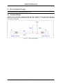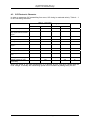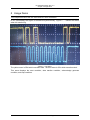
1
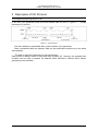
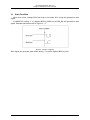
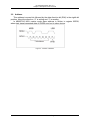
Fujitsu Semiconductor (Shanghai) Co., Ltd.
Application Note
MCU-AN- 500050-E-10
F²MC-8FX FAMILY
8-BIT MICROCONTROLLER
MB95310/370 SERIES
I2C HARDWARE DESIGN API
APPLICATION NOTE
I2C Hardware Design API V1.0
Revision History
Revision History
Date
2009-11-10
Author
Jane Li
Change of Records
V1.0, First draft
This manual contains 17 pages.
1. The products described in this manual and the specifications thereof may be changed without prior notice.
To obtain up-to-date information and/or specifications, contact your Fujitsu sales representative or Fujitsu
authorized dealer.
2. Fujitsu will not be liable for infringement of copyright, industrial property right, or other rights of a third party
caused by the use of information or drawings described in this manual.
3. The contents of this manual may not be transferred or copied without the express permission of Fujitsu.
4. The products contained in this manual are not intended for use with equipments which require extremely
high reliability such as aerospace equipments, undersea repeaters, nuclear control systems or medical
equipments for life support.
5. Some of the products described in this manual may be strategic materials (or special technology) as defined
by the Foreign Exchange and Foreign Trade Control Law. In such cases, the products or portions thereof
must not be exported without permission as defined under the law.
© 2009 Fujitsu Semiconductor (Shanghai) Co., Ltd
MCU-AN- 500050-E-10 – Page 2
I2C Hardware Design API V1.0
CONTENTS
CONTENTS
REVISION HISTORY .............................................................................................................. 2 CONTENTS ............................................................................................................................ 3 1 INTRODUCTION ................................................................................................................ 4 2 BACKGROUND ................................................................................................................. 5 3 DESCRIPTION OF I2C PROTOCOL ................................................................................. 6 3.1 Start Condition .......................................................................................................... 7 3.2 Address ..................................................................................................................... 8 3.3 Acknowledge ............................................................................................................. 9 3.4 Data .......................................................................................................................... 9 3.5 Stop Condition ........................................................................................................ 10 4 I2C HARDWARE DESIGN ............................................................................................... 11 4.1 Hardware Design .................................................................................................... 11 4.2 Pull Up Resister ...................................................................................................... 12 4.3 I2C Electronic Character ......................................................................................... 13 5 USAGE DEMO ................................................................................................................. 14 6 ADDITIONAL INFORMATION ......................................................................................... 16 7 APPENDIX ....................................................................................................................... 17 7.1 Figures .................................................................................................................... 17 7.2 Table ....................................................................................................................... 17 MCU-AN- 500050-E-10 – Page 3
I2C Hardware Design API V1.0
Chapter 1 Introduction
1 Introduction
This document introduces API for I2C hardware design.
I2C is two wires synchronization protocol in device communication, which has bi-directional
wires SDA and SCL. In following chapters we will describe the I2C hardware design and
protocol.
MCU-AN- 500050-E-10 – Page 4
I2C Hardware Design API V1.0
Chapter 2 Background
2 Background
This chapter introduces the background of I2C.
In serial extended interface protocol, there are SPI of MOTOROLA, PLUS of NS and I2C
of Philips. Compared with others, the I2C is used widely. I2C bus has standard criterion and
multitudinous periphery apparatus.
The I2C interface is a two-wire, bi-directional bus consisting of a serial data line (SDA) and
a serial clock line (SCL). The devices connected to the bus via these two wires can
exchange data, and each device can operate as a sender or receiver in accordance with
their respective functions based on the unique address assigned to each device.
Following are some features of I2C:
¾
integrated Criterion
¾
independent Structure
¾
Easy to use
When I2C is used, typical use module of SCM is a small system. It can include I/O, keyboard,
display module, clock, A/D, data storage and so on. For what the software become easy and
content become more abundance.
MCU-AN- 500050-E-10 – Page 5
I2C Hardware Design API V1.0
Chapter 3 Description of I2C Protocol
3 Description of I2C Protocol
This chapter describes protocol of I2C.
In I2C bus, SCL generates clock and SDA reloads data out and in. Figure 3 – 1 simply
describes I2C protocol.
Figure 3 - 1 I2C Protocol
The slave address is transmitted after a start condition (S) is generated.
Data is transmitted after the address. Data can be transmitted continuously to the same
slave address.
The data is eight bits followed by an acknowledgment.
Data transfer is always ended in the master stop condition (P). However, the repeated start
condition can be used to transmit the address which indicates a different slave without
generating a stop condition.
MCU-AN- 500050-E-10 – Page 6
I2C Hardware Design API V1.0
Chapter 3 Description of I2C Protocol
3.1
Start Condition
When bus is free, change SDA from high to low while SCL is high will generate a start
signal.
In MB95F310 writing “1” to register IBCR10_MSS and ICCR0_EN will generate a start
signal. Detailed start status refer to Figure 3 – 2.
Figure 3 - 2 Status of Starting
Start signal can generate again when writing “1” to MCU register IBCR10_SCC.
MCU-AN- 500050-E-10 – Page 7
I2C Hardware Design API V1.0
Chapter 3 Description of I2C Protocol
3.2
Address
This address is seven bits followed by the data direction bit (R/W) in the eighth bit
position. About the direction, “0” is writing and “1” is reading
In MB95F310 MCU master mode slave address is written to register IDDR0,
when start signal generated data of IDDR0 send out to slave device.
Figure 3 - 3 Status of Address
MCU-AN- 500050-E-10 – Page 8
I2C Hardware Design API V1.0
Chapter 3 Description of I2C Protocol
3.3
Acknowledge
Acknowledge is generated when slave device received address or data. Acknowledge is
low level when SCL is in the ninth pulse.
Figure 3 - 4 Status of Acknowledge
If the SDA is high at the ninth pulse, which indicates that the slave device didn’t receive the
address or data from master device.
3.4
Data
Whatever writing to/reading from slave device the data is eight bits. Only when master
device received the acknowledge data can transmitted out. In MB95F310 MCU the register
IDDR0 is used to save the data.
MCU-AN- 500050-E-10 – Page 9
I2C Hardware Design API V1.0
Chapter 3 Description of I2C Protocol
3.5
Stop Condition
When SCL is high, changing SDA from low to high will generate a stop signal. In
MB95F310 MCU writes “0” to register IBCR10_MSS will generate a stop signal.
Figure 3 - 5 Status of Stop
MCU-AN- 500050-E-10 – Page 10
I2C Hardware Design API V1.0
Chapter 4 I2C Hardware Design
4 I2C Hardware Design
This chapter describes hardware design of I2C.
4.1
Hardware Design
Actually, I2C is two wires, which are SDA and SCL. Master SDA is connected with slave
SDA, and master SCL is connected with slave SCL. Figure 4 – 1 describes the hardware
connection in detailed.
Figure 4 - 1 I2C Hardware Design
MCU-AN- 500050-E-10 – Page 11
I2C Hardware Design API V1.0
Chapter 4 I2C Hardware Design
4.2
Pull Up Resister
Because the start signal is generated when SCL is high, so user must connect pull up
resister to I2C.
The pull up resister is restricted by power voltage. That is because when voltage VOLMAX is
0.4V, the Min current must be 3mA. Figure 4 – 2 describes the relationship between power
voltage VDD and pull up resister RP, pull up resister RP and RS.
Figure 4 - 2 Resister of Pull Up
MCU-AN- 500050-E-10 – Page 12
I2C Hardware Design API V1.0
Chapter 4 I2C Hardware Design
4.3
I2C Electronic Character
In order to guarantee I2C transmitting from error, I2C timing is restricted strictly. Table 4 – 1
is I2C bus timing character.
Table 4 - 1 I2C Timing
Standard Mode
Parameter
High Speed Mode
Unit
MIN
MAX
MIN
MAX
0
100
0
400
kHz
4.7
-
1.3
-
µs
4
-
0.6
-
µs
SCL cycle of low level
4.7
-
1.3
-
µs
SCL cycle of high level
4
-
0.6
-
µs
Building time of double start
signal
4.7
-
0.6
-
µs
Data building time
250
-
100
-
ns
Rising time of SDA and SCL
-
1000
20
300
ns
Dropping time of SDA and
SCL
-
300
20
300
ns
Building time of stop signal
4
-
0.6
-
µs
Reload Capacity of every
transmitting
-
400
-
400
pF
SCL Frequency
Vacant time between first
stop signal and second start
signal
Start holding time
About the speed of I2C data transmission it is decided by SCL high level voltage and low
level voltage. In actually the transmitting speed can be modified by adding delay for SCL.
MCU-AN- 500050-E-10 – Page 13
I2C Hardware Design API V1.0
Chapter 5 Usage Demo
5 Usage Demo
This chapter describes the I2C wave and I2C multi connection.
In I2C transmitting the signal is transferred synchronously. Figure 5 - 1 shows the status
when bit transferring.
Figure 5 - 1 I2C Wave
The yellow wave is SDA which transfers data. The blue wave is SCL which transfers clock.
This wave displays the start condition, data transfer condition, acknowledge generate
condition, and stop condition.
MCU-AN- 500050-E-10 – Page 14
I2C Hardware Design API V1.0
Chapter 5 Usage Demo
One master I2C device can control several I2C devices. Every slave device has only
address. When the slave device received the address which is same as itself, the slave
device generates acknowledge to master, and then begin to receive data.
Figure 5 – 2 describes the situation when one master controls several slave device.
Figure 5 - 2 I2C Multi-connection
MCU-AN- 500050-E-10 – Page 15
I2C Hardware Design API V1.0
Chapter 6 Additional Information
6 Additional Information
For more information about how to use MB95310 EV-board, BGM Adaptor and SOFTUNE,
please refer to EV-Board MB2146-450-E User Manual, or visit websites:
English version:
http://www.fujitsu.com/cn/fsp/services/mcu/mb95/application_notes.html
Simplified Chinese Version:
http://www.fujitsu.com/cn/fss/services/mcu/mb95/application_notes.html
MCU-AN- 500050-E-10 – Page 16
I2C Hardware Design API V1.0
Chapter 7 Appendix
7 Appendix
7.1
Figures
Figure 3 - 1 I2C Protocol .......................................................................................................... 6 Figure 3 - 2 Status of Starting .................................................................................................. 7 Figure 3 - 3 Status of Address ................................................................................................. 8 Figure 3 - 4 Status of Acknowledge ......................................................................................... 9 Figure 3 - 5 Status of Stop ..................................................................................................... 10
Figure 4 - 1 I2C Hardware Design ......................................................................................... 11 Figure 4 - 2 Resister of Pull Up .............................................................................................. 12
Figure 5 - 1 I2C Wave ............................................................................................................ 14 Figure 5 - 2 I2C Multi-connection ........................................................................................... 15 7.2
Table
Table 4 - 1 I2C Timing ........................................................................................................... 13
MCU-AN- 500050-E-10 – Page 17