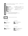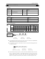
1
1
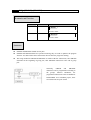
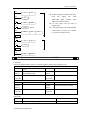
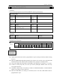
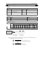
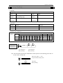
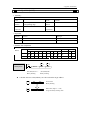
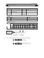
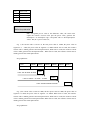
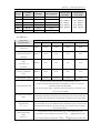
Program Summary
XC series PLC as the controllers, accept the signal and execute the program in the
controller, to fulfill the requirements from the users. In this chapter, we start with the
program forms, introduce the main features, the supported two program languages etc.
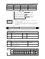
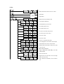
1-1.Programmer Controller’s Features
1-2.Program Language
1-3.Program Format
1-1.Program Controller’s Features
Program Language
XC series PLC support two kinds of program languages, instruction list and ladder,
the two languages can convert to the other;
Security of the Program
To avoid the stolen or wrong modifying of user program, we encrypt the program.
When uploading the encrypted program, it will check in the form of password. This
can maintain the user’s copyright; meantime, it limits the download, to avoid the
modification with the program spitefully.
Program’s comments
When the user program is too long, adding comments to the program and its soft
components is necessary.
Offset Function
Add offset appendix (like X3[D100]、M10[D100]、D0[D100]) behind coils, data
registers can realize indirect addressing. For example, when D100=9, X3[D100]=X14;
M10[D100]=M19, D0[D100]=D9
Rich Basic Functions
l
l
XC series PLC offers enough basic instructions, can fulfill basic sequential
control, data moving and comparing, arithmetic operation, logic control, data
loop and shift etc.
XC series PLC also support special compare, high speed pulse, frequency testing,
precise time, PID control, position control etc for interruption, high speed counter
(HSC).
C Language Function Block
XC series PLC support C language function block, users can call the edited function
block freely. This function reduces the program quantity greatly.
Stop when power ON Function
XC series PLC support “Stop when power on PLC” function. With this function,
when there is a serious problem during PLC running, use this method to stop all
output immediately. Besides, with this method, connect PLC when parameters are set
wrongly.
Communication Function
XC series PLC support many communication formats, like basic Modbus
communication, CABBUS communication, free format communication. Besides, via
special network module, connect to Ether net, GPRS net.
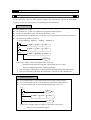
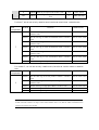
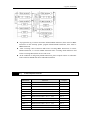
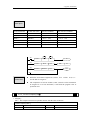
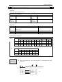
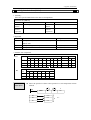
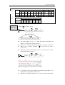
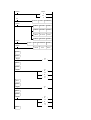
1-2.Program Language
1-2-1.Type
XC series PLC support two types of program language:
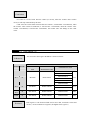
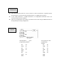
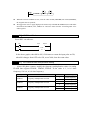
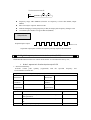
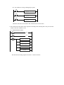
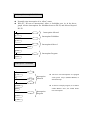
Instruction List
Instruction list inputs in the form of “LD”, “AND”, “OUT” etc. This is the basic input
form of the programs, but it’s hard to read and understand;
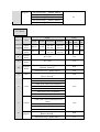
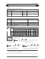
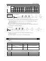
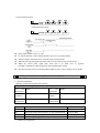
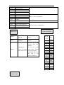
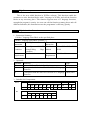
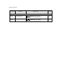
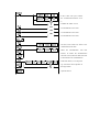
E.g.:
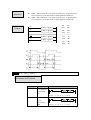
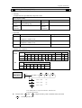
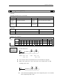
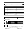
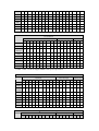
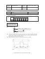
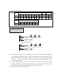
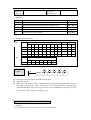
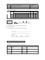
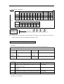
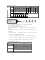
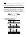
Step
0
1
2
3
Instruction
LD
OR
ANI
OUT
Soft Components
X000
Y005
X002
Y005
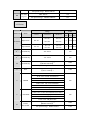
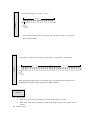
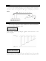
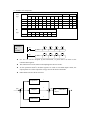
Ladder
With sequential control signal and soft components, draw the sequential control graph
on program interface, this method is called “Ladder”. This method use coil signs etc.
to represent sequential circuit, so it’s easier to understand the program. Meantime,
monitor PLC with the circuit’s status.
E.g.:
X0
X2
Y5
Y5
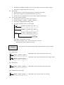
1-2-2.Alternation
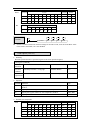
Convert the above two methods freely:
Instruction
Ladder
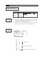
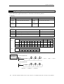
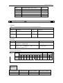
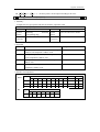
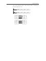
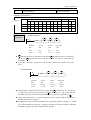
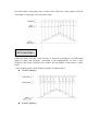
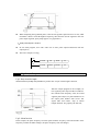
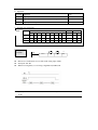
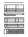
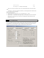
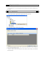
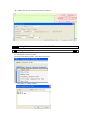
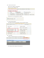
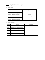
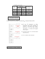
1-3.Program Format
Direct Input
The above two program methods can input in the correspond interface separately, especially in the
ladder window, there is a instruction hint function, which improves the program efficiency greatly;
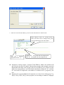
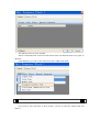
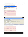
Panel Configuration
As in XC series PLC, there are many instructions which has complicate usage and
many using methods, like pulse output instruction, main unit PID etc. XCPPro also
support the configure interface for these special instructions. In the correcpond
configure interface, input the parameters and ID according to the requirements will be
ok;
For the details of panel configuration, please refer《XC series PLC user manual【software part】》
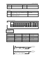
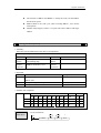
2
Soft Component’s Function
In chapter 1, we briefly tell the program language of XC series PLC. However, the most important
element to a program is the operands. These elements relate to the relays and registers inside the
controller. In this chapter, we will describe the functions and using methods of these relays and
registers.
2-1.Summary of the Soft Components
2-2.Structure of the Soft Components
2-3.List of the Soft Components
2-4.Input/output Relays (X、Y)
2-5.Auxiliary Relays (M)
2-6.Status Relays (S)
2-7.Timers (T)
2-8.Counters (C)
2-9.Data Registers (D)
2-10.Constant (K、H)
2-11.Pointer (P、I)
2-12.Program Principle
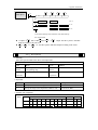
2-1.Summary of the Soft Components
There are many relays, timers and counters inside PLC. They all have countless NO (Normally
ON) and NC (Normally Closed) contactors. Connect these contactors with the coils will make a
sequential control circuit. Below, we will introduce these soft components briefly;
Input Relay (X)
l Usage of the input relays
The input relays are used to accept the external ON/OFF signal, we use X to state.
l Address Specify Principle
Ø
Ø
In each basic unit, specify the ID of input relay, output relay in the form of
X000~X007,X010~X017…,Y000~Y007,Y010~Y017… (octal form)
The expansion module’s ID obeys the principle of channel 1 starts from X100/Y100,
channel 2 starts from X200/Y200… 7 expansions can be connected in total.
l Points to pay attention when using
Ø
Ø
For the input relay’s input filter, we use digital filter. Users can change the filter
parameters via relate settings.
We equip enough output relays inside PLC; for the output relays beyond the
input/output points, use them as auxiliary relays, program as normal contactors/coils.
Output Relay(Y)
l Usage of the output relays
Output relays are the interface of drive external loads, represent with sign Y;
l
Address Assignment Principle
Ø
Ø
In each basic unit,assign the ID of output relays in the form of Y000~Y007,
Y010~Y017… this octal format.
The ID of expansion obeys the principle of: channel 1 starts from Y100, channel 2 starts
from Y200… 7 expansions could be connected totally.
Auxiliary Relays(M)
l Usage of Auxiliary Relays
Auxiliary relays are equipped inside PLC, represent with the sign of M;
l Address assignment principle
In basic units, assign the auxiliary address in the form of decimal
l Points to note
Ø This type of relays are different with the input/output relays, they can’t get external load,
can only use in program;
Ø Retentive relays can keep its ON/OFF status in case of PLC power OFF;
Status Relays(S)
l Usage of status relays
Used as relays in Ladder, represent with “S”
l Address assignment principle
In basic units, assign the ID in the form of decimal
l Points to note
If not used as operation number, they can be used as auxiliary relays, program as
normal contactors/coils. Besides, they can be used as signal alarms, for external
diagnose.
Timer(T)
l Usage of the timers
Timers are used to calculate the time pulse like 1ms, 10ms, 100ms etc. when reach the
set value, the output contactors acts, represent with “T”
l
Address assignment principle
In basic units, assign the timer’s ID in the form of decimal. But divide ID into several parts
according to the clock pulse, accumulate or not. Please refer to chapter 2-2 for details.
l Time pulse
There are three specifications for the timer’s clock pulse: 1ms、10ms、100ms. If choose 10ms timer,
carry on addition operation with 10ms time pulse;
l Accumulation/not accumulation
The times are divided into two modes: accumulation time means even the timer coil’s driver is
OFF, the timer will still keep the current value; while the not accumulation time means when the
count value reaches the set value, the output contact acts, the count value clears to be 0;
Counter(C)
According to different application and purpose, we can divide the counters to different types as
below:
l For internal count (for general using/power off retentive usage)
Ø
Ø
Ø
16 bits counter: for increment count, the count range is 1~32,767
32 bits counter: for increment count, the count range is 1~2,147,483,647
These counters can be used by PLC’s internal signal. The response speed is one scan
cycle or longer.
l For High Speed Count (Power off retentive)
Ø
32 bits counter: for increment/decrement count, the count range is -2,147,483,648~
+2,147,483,647
(single phase increment count, single phase increment/decrement count, AB phase cont)
specify to special input points (
Ø
The high speed counter can count 80KHz frequency, it separates with the PLC’s scan
cycle;
Data Register(D)
l Usage of Data Registers
Data Registers are used to store data, represent with “D”
l Addressing Form
The data registers in XC series PLC are all 16 bits (the highest bit is the sign bit), combine
two data registers together can operate 32 bits (the highest bit is the sign bit) data process.
l Points to note
Same with other soft components, data registers also have common usage type and power off
retentive type.
FlashROM Register(FD)
l Usage of FlashROM registers
FlashROM registers are used to store data soft components, represent with “FD”
l Addressing Form
In basic units, FlashROM registers are addressed in form of decimal;
l Points to note
Even the battery powered off, this area can keep the data. So this area is used to store
important parameters. FlashROM can write in about 1,000,000 times, and it takes time at
every write. Frequently write can cause permanent damage of FD.
Constant(B)(K)(H)
l In every type of data in PLC, B represents Binary, K represents Decimal, H represents
Hexadecimal. They are used to set timers and counters value, or operands of application
instructions.
2-2.Structure of Soft Components
2-2-1.Structure of Memory
In XC series PLC, there are many registers. Besides the common data registers D, FlashROM
registers, we can also make registers by combining bit soft components.
Data Register D
l
l
l
l
l
For common use, 16 bits
For common use, 32 bits (via combine two sequential 16 bits registers)
For power off retentive usage, can modify the retentive zone
For special usage, occupied by the system, can’t be used as common instruction’s parameters
For offset usage (indirect specifies)
Ø Form: Dn[Dm]、Xn[Dm] 、Yn[Dm] 、Mn[Dm] etc.
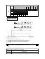
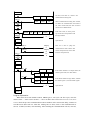
M8002
M2
M8000
MOV
K0
D0
MOV
K5
D0
MOV
D10[D0]
D100
Y0[D0]
In the above sample, if D0=0, then D100=D10, Y0 is ON.
If M2 turns from OFF to be ON, D0=5, then D100=D15, Y5 is ON.
Therein, D10[D0]=D[10+D0],Y0[D0]=Y[0+D0]。
Ø The word offset combined by bit soft components: DXn[Dm] represents DX[n+Dm]。
Ø The soft components with offset, the offset can be represent by soft component D.
Timer T/Counter C
l
l
l
For common usage, 16 bits, represent the current value of timer/counter;
For common usage, 32 bits, (via combine two sequential 16 bits registers)
To represent them, just use the letter+ID method, such as T10, C11.
E.g.
X0
M0
T11
T11
MOV
T11
K99
D0
Y1
In the above example, MOV T11 D0, T11 represents word register;
LD T11, T11 represents bit register.
FlashROM Register FD
l
l
l
For power off retentive usage, 16 bits
For power off retentive usage, 16 bits, (via combine two sequential 16 bits registers)
For special usage, occupied by the system, can’t be used as common instruction’s
parameters
Expansion’s internal register ED
l
l
For common usage, 16 bits,
For common usage, 32 bits, (via combine two sequential 16 bits registers)
Bit soft components combined to be register
l
l
l
l
l
For common usage, 16 bits, (via combine two sequential 16 bits registers)
The soft components which can be combined to be words are: X、Y、M、S、
T、C
Format: add “D” in front of soft components, like DM10, represents a 16
bits data from M10~M25
Get 16 points from DXn, but not beyond the soft components range;
The word combined by bit soft components can’t realize bit addressing;
E.g.:
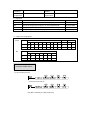
M0
M1
M8000
Ø
Ø
Ø
MOV
K21
DY0
MOV
K3
D0
MOV
DX2[D0]
D10
When M0 changes from OFF to be ON, the value in the word which is
combined by Y0~Y17 equals 21, i.e. Y0、Y2、Y4 becomes to be ON
Before M1 activates, if D0=0, DX2[D0] represents a word combined by
X2~X21
If M1 changes from OFF→ON, D0=3,then DX2[D0] represents a
2-2-2.Structure of Bit Soft Components
Bit soft components structure is simple, the common ones are X、Y、M、S、T、C, besides, a bit
of a register can also represents:
Relay
l
l
l
l
Input Relay X, octal type
Output Relay Y, octal type
Auxiliary Relay M、S, decimal type
Auxiliary Relay T、C, decimal type, as the represent method is same with
registers, so we need to judge if it’s word register or bit register according to
the register.
Register’s Bit
l
l
l
l
Composed by register’s bit, support register D
Represent method: Dn.m (0≤m≤15): the Nr.m bit of Dn register
The represent method of word with offset: Dn[Dm].x
Bit of Word can’t compose to be word again;
E.g.:
D0.4
D5[D1].4
Ø
Ø
Y0
Y1
D0.4 means when the Nr.4 bit of D0 is 1, set Y0 ON .
D5[D1].4 means bit addressing with offset, if D1=5, then D5[D1]
means the Nr.4 bit of D10
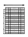
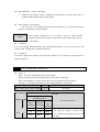
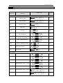
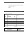
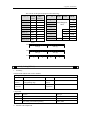
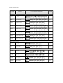
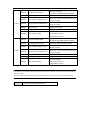
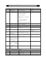
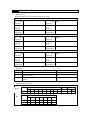
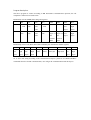
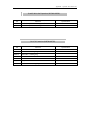
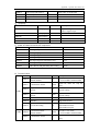
2-3.Soft Components List
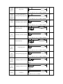
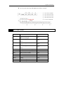
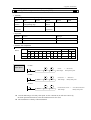
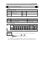
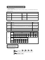
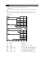
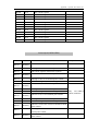
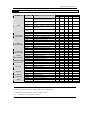
2-3-1.Soft Components List
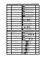
XC1 Series
Mnemonic
※1
I/O points
X
Y
※2
※3
Name
Range
points
10I/O
16 I/O
24 I/O
X0~X4
X0~X7
X0~X13
X0~X17
5
8
12
16
Output Points Y0~Y4
Y0~Y7
Y0~Y13
Y0~Y17
5
8
12
16
Input Points
Internal Relay
X0~X77
Internal Relay
Y0~Y77
32 I/O 10 I/O 16 I/O 24 I/O 32 I/O
64
64
※4
M0~M199【M200~M319】
For Special Usage
M
Internal Relay
For Special Usage
For Special Usage
For Special Usage
For Special Usage
S
Flow
320
※5
M8000~M8079
※5
M8120~M8139
※5
M8170~M8172
128
※5
M8238~M8242
※5
M8350~M8370
S0~S31
32
T0~T23: 100ms not accumulation
T100~T115: 100ms accumulation
T
Timer
T200~T223: 10ms not accumulation
T300~T307: 10ms accumulation
80
T400~T403: 1ms not accumulation
T500~T503: 1ms accumulation
C0~C23: 16 bits forward counter
C300~C315: 32 bits forward/backward
counter
C
Counter
C600~C603: single-phase HSC
48
C620~C621
C630~C631
D0~D99【D100~D149】
For Special Usage
For Special Usage
D
Data Register
For Special Usage
For Special Usage
For Special Usage
For Special Usage
FD
FlashROM
※4
150
※5
D8000~D8029
※5
D8060~D8079
※5
D8120~D8179
※5
D8240~D8249
138
※5
D8306~D8313
※5
D8460~D8469
FD0~FD411
412
Register
※6
For Special Usage
For Special Usage
For Special Usage
For Special Usage
For Special Usage
※5
FD8000~FD8011
※5
FD8202~FD8229
※5
98
FD8306~FD8315
※5
FD8323~FD8335
※5
FD8350~FD8384
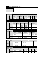
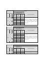
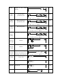
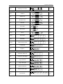
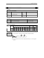
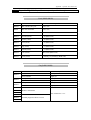
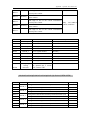
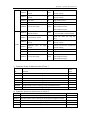
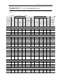
XC2 Series
Range
Mnemonic
Name
I/O Points
※1
X
Y
※2
※3
M
S
Points
14 16
I/O I/O
14 I/O
16 I/O
24/32 I/O
48/60 I/O
Input
Points
X0~X7
X0~X7
X0~X15
X0~X21
X0~X33
X0~X43
8
Output
Points
Y0~Y5
Y0~Y7
Y0~Y11
Y0~Y15
Y0~Y23
Y0~Y27
6
24/32
I/O
48/60
I/O
8
14/18
28/36
8
10/14
20/24
Internal
Relay
X0~X1037
544
Internal
Relay
Y0~Y1037
544
M0~M2999
※
【M3000~M7999】 4
8000
Internal
Relay
Flow
※
For Special Usage 5M8000~M8767
768
S0~S511
※
【S512~S1023】 4
1024
T0~T99: 100ms not accumulation
T100~T199: 100ms accumulation
T200~T299: 10ms not accumulation
T
Timer
T300~T399: 10ms accumulation
640
T400~T499: 1ms not accumulation
T500~T599: 1ms accumulation
T600~T639: 1ms precise time
C0~C299: 16 bits forward counter
C
Counter
C300~C599: 32 bits forward/backward
counter
C600~C619: single-phase HSC
640
C620~C629: double-phase HSC
C630~C639: AB phase HSC
D
Data
Register
D0~D999
※
【D4000~D4999】 4
※
For Special Usage 5D8000~D8511
2000
612
※
For Special Usage 5D8630~D8729
FD
FLASH
Register
FD0~FD127
128
※
For Special Usage 5FD8000~FD8383
384
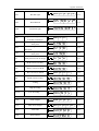
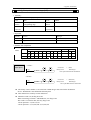
XC3 Series
Range
Mnemonic
Name
Points
14 24/32 48/60
I/O I/O I/O
14 I/O
24/32 I/O
48/60 I/O
Input Points
X0~X7
X0~X15
X0~X21
X0~X33
X0~X43
8
14/18 28/36
Output Points
Y0~Y5
Y0~Y11
Y0~Y15
Y0~Y23
Y0~Y27
6
10/14 20/24
I/O Points
※1
X
Y
※2
※3
M
Internal Relay
X0~X1037
544
Internal Relay
Y0~Y1037
544
Internal Relay
M0~M2999
※
【M3000~M7999】 4
8000
※
S
Flow
For Special Usage 5M8000~M8767
768
S0~S511
※
【S512~S1023】 4
1024
T0~T99: 100ms not accumulation
T100~T199: 100ms accumulation
T200~T299: 10ms not accumulation
T
TIMER
T300~T399: 10ms accumulation
640
T400~T499: 1ms not accumulation
T500~T599: 1ms accumulation
T600~T639: 1ms precise time
C0~C299: 16 bits forward counter
C300~C599: 32 bits forward/backward counter
C
COUNTER
C600~C619: single-phase HSC
640
C620~C629: double-phase HSC
C630~C639: AB phase HSC
D
DATA
REGISTER
D0~D3999
※
【D4000~D7999】 4
※
For Special Usage 5D8000~D9023
8000
1024
FD
ED
※7
FlashROM
※
REGISTER 6
FD0~FD1535
1536
※
For Special Usage 5FD8000~FD8511
512
ED0~ED16383
16384
EXPANSION’S
INTERNAL
REGISTER
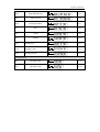
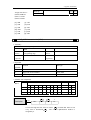
XC5 Series
Mnemonic
Name
I/O RANGE
POINTS
24/32 I/O
48/60 I/O
Input Points
X0~X15
X0~X21
X0~X33
X0~X43
14/18
28/36
Output Points
Y0~Y11
Y0~Y15
Y0~Y23
Y0~Y27
10/14
20/24
I/O Points
24/32 I/O 48/60 I/O
※1
X
Y
※2
※3
M
Internal Relay
X0~X1037
544
Internal Relay
Y0~Y1037
544
8000
Internal Relay
M0~M3999
※
【M4000~M7999】 4
※
S
Flow
For Special Usage 5M8000~M8767
768
S0~S511
※
【S512~S1023】 4
1024
T0~T99: 100ms not accumulation
T100~T199: 100ms accumulation
T200~T299: 10ms not accumulation
T
TIMER
T300~T399: 10ms accumulation
640
T400~T499: 1ms not accumulation
T500~T599: 1ms accumulation
T600~T639: 1ms precise time
C0~C299: 16 bits forward counter
C300~C599: 32 bits forward/backward counter
C
COUNTER
C600~C619: single-phase HSC
640
C620~C629: double-phase HSC
C630~C639: AB phase HSC
D
FD
DATA
REGISTER
FlashROM
D0~D3999
※
【D4000~D7999】 4
※
8000
For Special Usage 5D8000~D9023
1024
FD0~FD5119
5120
※6
ED
※7
REGISTER
For Special Usage 5FD8000~FD9023
1024
EXPANSION’S
INTERNAL
REGISTER
ED0~ED36863
36864
I/O range
Points
※
XCM Series
Mnemonic
I/O Points
Name
24/32 I/O
48 I/O
24/32 I/O
48 I/O
Input Points
X0~X15
X0~X21
X0~X33
14/18
28
Output Points
Y0~Y11
Y0~Y15
Y0~Y23
10/14
20
※1
X
Y
※2
※3
M
Internal Relay
X0~X1037
544
Internal Relay
Y0~Y1037
544
Internal Relay
M0~M2999
※
【M3000~M7999】 4
8000
※
S
Flow
For Special Usage 5M8000~M8767
768
S0~S511
※
【S512~S1023】 4
1024
T0~T99: 100ms not accumulation
T100~T199: 100ms accumulation
T200~T299: 10ms not accumulation
T
TIMER
T300~T399: 10ms accumulation
640
T400~T499: 1ms not accumulation
T500~T599: 1ms accumulation
T600~T639: 1ms precise time
C0~C299: 16 bits forward counter
C
COUNTER
C300~C599: 32 bits forward/backward
counter
C600~C619: single-phase HSC
640
C620~C629: double-phase HSC
C630~C639: AB phase HSC
D
FD
DATA
REGISTER
FlashROM
D0~D2999
※
【D4000~D4999】 4
※
4000
For Special Usage 5D8000~D9023
1024
FD0~FD63
64
※6
REGISTER
※
For Special Usage 5FD8000~FD8349
※
For Special Usage 5FD8890~FD8999
ED
※7
EXPANSION’S
INTERNAL
REGISTER
ED0~ED36863
460
36864
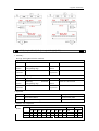
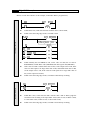
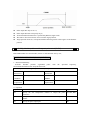
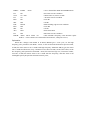
※1: I/O points, means the terminal number that users can use to wire the input, output
※2: X, means the internal input relay, the X beyond Input points can be used as middle relay;
※3: Y, means the internal output relay, the Y beyond Output points can be used as middle relay;
※4: The memory zone in【
】 is power off retentive zone, soft components D、M、S、T、C can change the
retentive area via setting. Please refer to 2-3-2 for details;
※5: for special use, means the special registers occupied by the system, can’t be used for other purpose. Please
refer to Appendix 1.
※6: FlashROM registers needn’t set the power off retentive zone, when power is off (no battery), the data will not
lose
※7: Expansion’s internal register ED, require PLC hardware V3.0 or above
※8: Input coils、output relays are in octal form, the other registers are in decimal form;
※9: The I/O that are not wired with external device can be used as fast internal relays;
※10: for the soft components of expansion devices, please refer to relate manuals;
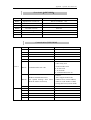
2-3-2.Power Off Retentive Zone
The power off retentive area of XC series PLC are set as below, this area can be set by user again;
Soft
components
XC1
Series
XC2
Series
XC3
Series
XC5
Series
XCM
Series
SET
AREA
FUNCTION
System’s
default
value
Retentive
Zone
100
D100~D149
D
FD8202 Start tag of D power off retentive zone
M
FD8203
Start tag of M power off retentive
zone
200
M200~M319
T
FD8204
Start tag of T power off retentive zone
640
Not set
C
FD8205
Start tag of C power off retentive zone
320
C320~C631
S
FD8206
Start tag of S power off retentive zone
512
S0~S31
D
FD8202 Start tag of D power off retentive zone
4000
D4000~D4999
M
FD8203
Start tag of M power off retentive
zone
3000
M3000~M7999
T
FD8204
Start tag of T power off retentive zone
640
Not set
C
FD8205
Start tag of C power off retentive zone
320
C320~C639
S
FD8206
Start tag of S power off retentive zone
512
S512~S1023
D
FD8202 Start tag of D power off retentive zone
4000
D4000~D7999
M
FD8203
Start tag of M power off retentive
zone
3000
M3000~M7999
T
FD8204
Start tag of T power off retentive zone
640
Not set
C
FD8205
Start tag of C power off retentive zone
320
C320~C639
S
FD8206
Start tag of S power off retentive zone
512
S512~S1023
ED
FD8207
Start tag of ED power off retentive
zone
0
ED0~ED16383
4000
D4000~D7999
D
FD8202 Start tag of D power off retentive zone
M
FD8203
Start tag of M power off retentive
zone
4000
M4000~M7999
T
FD8204
Start tag of T power off retentive zone
640
Not set
C
FD8205
Start tag of C power off retentive zone
320
C320~C639
S
FD8206
Start tag of S power off retentive zone
512
S512~S1023
ED
FD8207
Start tag of ED power off retentive
zone
0
ED0~ED36863
4000
D4000~D4999
D
FD8202 Start tag of D power off retentive zone
M
FD8203
Start tag of M power off retentive
zone
3000
M3000~M7999
T
FD8204
Start tag of T power off retentive zone
640
Not set
C
FD8205
Start tag of C power off retentive zone
320
C320~C639
S
FD8206
Start tag of S power off retentive zone
512
S512~S1023
ED
FD8207
Start tag of ED power off retentive
zone
0
ED0~ED36863
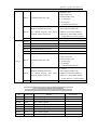
For timer T, we can set not only retentive zone, but also set certain timer’s retentive zone
Soft
Components
T
Set area
Function
Retentive Zone
FD8323
Set the start tag of 100ms not accumulation timer’s
retentive zone
The set value ~T99
FD8324
Set the start tag of 100ms accumulation timer’s retentive
zone
The set value~T199
FD8325
Set the start tag of 10ms not accumulation timer’s
retentive zone
The set value~T299
FD8326
Set the start tag of 10ms accumulation timer’s retentive
zone
The set value~T399
FD8327
Set the start tag of 1ms not accumulation timer’s
retentive zone
The set value~T499
FD8328
Set the start tag of 1ms accumulation timer’s retentive
zone
The set value~T599
FD8329
Set the start tag of 1ms precise timer’s retentive zone
The set value~T639
For counter C, we can set not only retentive zone, but also set certain counter’s retentive
zone
Soft
Components
Set area
Function
FD8330
Set the start tag of 16 bits positive counter’s retentive
zone
The set value~C299
FD8331
Set the start tag of 32 bits positive/negative counter’s
retentive zone
The set value~C599
FD8332
Set the start tag of single phase HSC’s retentive zone
The set value~C619
FD8333
Set the start tag of dual direction HSC’s retentive zone
The set value~C629
FD8334
Set the start tag of AB phase HSC’s retentive zone
The set value~C639
C
Retentive Zone
※1:if the whole power off retentive zone is smaller than the segment’s retentive area, then the segment’s area is
invalid. If the total counter’s set range is T200~T640, FD8324 value is 150, then the 100ms accumulate timer’s
retentive area T150~T199 is invalid.
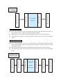
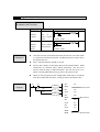
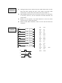
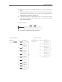
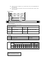
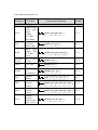
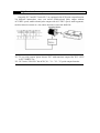
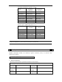
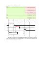
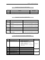
2-4.Input/output relays(X、Y)
Number List
XC series PLC’s input/output are all in octal form, each series numbers are listed below:
Range
Series
XC1
Name
Points
16
24 I/O 32 I/O
I/O
10I/O
16 I/O
24 I/O
32 I/O
10 I/O
X
X0~X4
X0~X7
X0~X13
X0~X17
5
8
12
16
Y
Y0~Y4
Y0~Y7
Y0~Y13
Y0~Y17
5
8
12
16
Range
Series
Name
Points
14 I/O
16 I/O
24/32 I/O
48/60 I/O
14
I/O
X
X0~X7
X0~X7
X0~X15
X0~X21
X0~X33
X0~X43
8
8
14/18
28/36
Y
Y0~Y5
Y0~Y7
Y0~Y11
Y0~Y15
Y0~Y23
Y0~Y27
6
8
10/14
20/24
XC2
16
48/60
24/32 I/O
I/O
I/O
Range
Series
Name
24/32 I/O
48/60 I/O
X
X0~X7
X0~X15
X0~X21
X0~X33
X0~X43
8
14/18
28/36
Y
Y0~Y5
Y0~Y11
Y0~Y15
Y0~Y23
Y0~Y27
6
10/14
20/24
Name
Range
Points
24/32 I/O
48/60 I/O
24/32 I/O
48/60 I/O
X
X0~X15
X0~X21
X0~X33
X0~X43
14/18
28/36
Y
Y0~Y11
Y0~Y15
Y0~Y23
Y0~Y27
10/14
20/24
XC5
Series
14 I/O 24/32 I/O
48/60
I/O
14 I/O
XC3
Series
Points
Name
Range
Points
24 I/O
32 I/O
48 I/O
24 I/O
32 I/O 48 I/O
X
X0~X15
X0~X21
X0~X33
14
18
28
Y
Y0~Y11
Y0~Y15
Y0~Y23
10
14
20
XCM
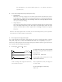
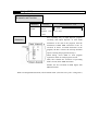
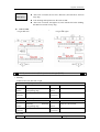
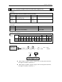
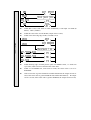
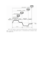
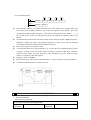
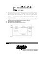
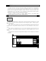
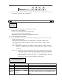
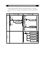
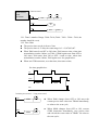
Function
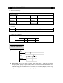
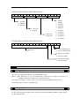
External Signal Output
Output Terminal Y
Input Terminal X
External Signal Input
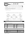
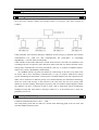
XC series PLC
CPU unit
Input Relay X
l
l
l
PLC’s input terminals are used to accept the external signal input, while the input relays are a
type of optical relays to connect PLC inside and input terminals;
The input relays have countless normally ON/OFF contactors, they can be used freely;
The input relays which are not connected with external devices can be used as fast internal
relays;
Output Relay Y
l
l
l
PLC’s output terminals can be used to send signals to external loads. Inside PLC, output
relay’s external output contactors (including relay contactors, transistor’s contactors) connect
with output terminals.
The output relays have countless normally ON/OFF contactors, they can be used freely;
The output relays which are not connected with external devices can be used as fast internal
relays;
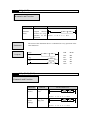
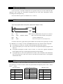
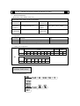
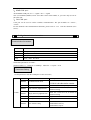
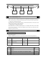
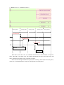
Execution Order
External Signal Output
Output Terminal Y
Program
Dispose Area
Output Image Area
Input Image Area
Input Terminal X
External Signal Input
XC series PLC
CPU unit
l
l
Input Disposal
Ø Before PLC executing the program, read every input terminal’s ON/OFF status of PLC
to the image area.
Ø In the process of executing the program, even the input changed, the content in the input
image area will not change. However, in the input disposal of next scan cycle, read out
the change.
Output Disposal
Ø Once finish executing all the instructions, transfer the ON/OFF status of output Y image
area to the output lock memory area. This will be the actual output of the PLC.
Ø The contacts used for the PLC’s external output will act according to the device’s
response delay time.
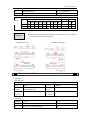
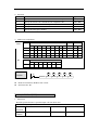
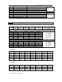
2-5.Auxiliary Relay (M)
Number List
The auxiliary relays M in XC series PLC are all in decimal form, please refer the details from
tables below:
RANGE
SERIES NAME
FOR COMMON
USE
FOR POWER-OFF
RETENTIVE USE
FOR SPECIAL USE
M8000~M8079
M8120~M8139
XC1
M
M000~M199
M200~M319
M8170~M8172
M8238~M8242
M8350~M8370
RANGE
SERIES NAME
XC2
M
FOR COMMON
USE
FOR POWER-OFF
RETENTIVE USE
FOR SPECIAL USE
M000~M2999
M3000~M7999
M8000~M8767
RANGE
SERIES NAME
XC3
M
SERIES NAME
FOR COMMON
USE
FOR POWER-OFF
RETENTIVE USE
FOR SPECIAL USE
M000~M2999
M3000~M7999
M8000~M8767
RANGE
XC5
M
FOR COMMON
USE
FOR POWER-OFF
RETENTIVE USE
FOR SPECIAL USE
M000~M3999
M4000~M7999
M8000~M8767
RANGE
SERIES NAME
XCM
M
FOR COMMON
USE
FOR POWER-OFF
RETENTIVE USE
FOR SPECIAL USE
M000~M2999
M3000~M7999
M8000~M8767
Function
In PLC, auxiliary relays M are used frequently. This type of relay’s coil is same with the output
relay. They are driven by soft components in PLC;
auxiliary relays M have countless normally ON/OFF contactors. They can be used freely, but this
type of contactors can’t drive the external loads.
l For common use
Ø This type of auxiliary relays can be used only as normal auxiliary relays. I.e. if power
supply suddenly stop during the running, the relays will disconnect.
Ø Common usage relays can’t be used for power off retentive, but the zone can be
modified;
l
For Power Off Retentive Use
Ø The auxiliary relays for power off retentive usage, even the PLC is OFF, they can keep
the ON/OFF status before power OFF.
Ø Power off retentive zone can be modified by the user;
Ø Power off retentive relays are usually used to memory the status before stop the power,
then when power the PLC on again, the status can run again;
l
For Special Usage
Ø Special relays refer some relays which are defined with special meanings or functions,
start from M8000.
Ø There are two types of usages for special relays, one type is used to drive the coil, the
other type is used to the specified execution;
E.g.: M8002 is the initial pulse, activates only at the moment of start
M8033 is “all output disabled”
Ø Special auxiliary relays can’t be used as normal relay M;
2-6.Status Relay (S)
Address List
SERIES NAME
XC1
S
SERIES NAME
XC2
S
SERIES NAME
XC3
S
SERIES NAME
XC5
S
SERIES NAME
XCM
Function
l
l
l
S
XC series PLC’s status relays S are addressed in form of decimal; each
subfamily’s ID are listed below:
RANGE
FOR COMMON USE
FOR POWER-OFF RETENTIVE USE
S000~S031
-
RANGE
FOR COMMON USE
FOR POWER-OFF RETENTIVE USE
S000~S511
S512~S1023
RANGE
FOR COMMON USE
FOR POWER-OFF RETENTIVE USE
S000~S511
S512~S1023
RANGE
FOR COMMON USE
FOR POWER-OFF RETENTIVE USE
S000~S511
S512~S1023
RANGE
FOR COMMON USE
FOR POWER-OFF RETENTIVE USE
S000~S511
S512~S1023
Status relays are very import in ladder program; usually use them with
instruction “STL”. In the form on flow, this can make the program’s structure
much clear and easy to modify;
For common use
After shut off the PLC power, this type of relays will be OFF status;
For Power Off Retentive Use
Ø The status relays for power off retentive usage, even the PLC is OFF, they can keep the
ON/OFF status before power OFF.
Ø Power off retentive zone can be modified by the user;
The status relays also have countless “normally ON/OFF” contactors. So users can use them
freely in the program;
2-7.Timer (T)
Address List
SERIES NAME
XC series PLC’s timers T are addressed in form of decimal; each
subfamily’s ID are listed below:
RANGE
FOR COMMON USE
POINTS
T0~T23: 100ms not accumulation
T100~T115: 100ms accumulation
XC1
T
T200~T223: 10ms not accumulation
T300~T307: 10ms accumulation
80
T400~T403: 1ms not accumulation
T500~T503: 1ms accumulation
T0~T99: 100ms not accumulation
XC2
XC3
XC5
XCM
T100~T199: 100ms accumulation
T200~T299: 10ms not accumulation
T
T300~T399: 10ms accumulation
640
T400~T499: 1ms not accumulation
T500~T599: 1ms accumulation
T600~T639: 1ms with precise time
Function
The timers accumulate the 1ms, 10ms, 10ms clock pulse, the output contactor
activates when the accumulation reaches the set value;
We use OUT or TMR instruction to time for the normal timers. We use constant (K) to set the
value, or use data register (D) to indirect point the set value;
If X0 is ON, then T200 accumulate
10ms clock pulse based on the current
value; when the accumulation value
reaches the set value K200, the timer’s
output contact activates. I.e. the output
contact activates 2s later. If X0 breaks,
the timer resets, the output contact
resets;
l
Both OUT and TMR can realize the
time function. But if use OUT, the start
time is 0; if use TMR, the start time is 1
scan cycle
Normal Type
l
Accumulation Type
If X001 is ON, then T300 accumulate
10ms clock pulse based on the current
value; when the accumulation value
reaches the set value K2000, the timer’s
output contact activates. I.e. the output
contact activates 2s later.
Even if X0 breaks, the timer will
continue to accumulation on re-starting.
The accumulation time is 20ms;
If X002 is ON, the timer will be reset,
the output contacts reset;
Specify the set
value
T10 is the timer with 100ms as the
unit. Specify 100 as the constant, then
0.1s*100=10s timer works;
《Constant (K)》
X0
T10
K100
《Register (D)》
Timer Value
Action
Example
Write the value of indirect
data register in the
X0
MOV
K200
D5
program or input by value
switch.
X1
T10
D5
If set as the retentive
register, make sure the
battery voltage is enough,
or the value will be
unstable.
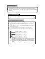
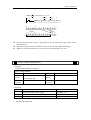
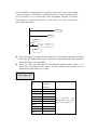
Timer T0~T599 is 16 bits linear increment mode (0~K32767), when the timer’s
value reaches the max value K32767, it stops timing. The timer’s status keeps
still;
《output delay OFF timer》
X0
Y0
T2
Y0
X0
T2
X0
K200
Y0
T2
When X000 is ON, output Y000;
When X000 from ON to OFF, delay T2(20s), then output Y000 is OFF.
《glitter》
X0
T2
T1
K20
T2
K10
X0
T1
T1
T2
T1
Y0
Y0
When X000 is ON, Y000 starts to glitter.
T1 controls the OFF time of Y000, T2 controls the ON time of Y000.
2-8.Counter ( C )
Number list
XC series PLC counters’ number are all decimal, please see the following
table for all the counter numbers.
RANGE
SERIES NAME
FOR COMMON USE
POINTS
C0~C23: 16 bits forward counter
C300~C315: 32 bits forward/backward counter
XC1
C
C600~C603: single-phase HSC
48
C620~C621
C630~C631
XC2
XC3
XC5
XCM
C0~C299: 16 bits forward counter
C300~C599: 32 bits forward/backward counter
C
C600~C619: single-phase HSC
640
C620~C629: double-phase HSC
C630~C639: AB phase HSC
All the counters number meaning:
TYPE
DESCRIPTION
16 bits forward counter
C0~C299
32 bits forward/backward
counter
C300~C599 (C300,C302...C598)(each occupies 2 counters
number) the number should be even
HSC
(High
Counter)
C600~C634(C600,C602...C634)( (each occupies 2 counters
number) the number should be even
Speed
※1: Please see chapter 5 for high speed counter.
Counter
characteristics
The characteristics of 16 bits and 32 bits counters:
Items
16 bits counter
32 bits counter
Count direction
Positive
Positive/negative
The set value
1~32,767
-2,147,483,648~+2,147,483,647
The assigned set
value
Constant K or data register
Same as the left, but data register must be in a
couple
Changing of the
current value
Change after positive count
Change after positive count (Loop counter)
Output contact
Hold the action
positive count
Hold the action after positive count, reset if
negative count
Reset activates
When executing RST command, counter’s current value is 0, output contacts
recover
The current value
register
16 bits
after
32 bits
The assignment of common use counters and power off retentive counters,
can me changed via FD parameters from peripheral devices;
Function
16 bits counter normal/retentive type
16 bits binary increment counters, the valid value is K1~K32,767 (decimal type
constant). The set value K0 and K1 has the same meaning. i.e. the output contact
works on the first count starts
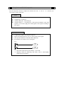
X0
X1
C0
l
l
l
RST
C0
C0
K10
If cut the PLC power supply, the normal
counter value become zero, the retentive
counter can store the value, it can
accumulate the value of last time.
Y0
When X001 is ON once, the counter increases 1. When the counter value is 10,
its output is activated. After, when the X001 is ON again, the counter continues
increasing 1.
If X000 is ON, reset counter, the counter value becomes zero.
It also can set the counter value in D register. For example, D10=123 is the same
as K123.
32 bits increase/decrease count range is +2147483648 ~ - 2147483647. Set the
increase or decrease count mode in M8238.
32 bits counter normal/retentive type
X2
X3
X4
C300
l
l
l
RST
C300
C300
K10
l
l
If M8238=1, it is decrease mode;
M8238=0, it is increase mode.
Set the count value in K or D, if set in D0
register, D0 and D1 will be seemed as one
32bits value.
X004 is ON, C300 starts to count.
Y1
If X003 is ON, reset the counter and C300 output.
If use retentive counter, the count value will be stored in PLC.
32 bits counter can be used as 32 bits register.
Set the count
value
u
l
M8238
It includes 16 bits and 32 bits count value.
16 bits counter
《set as constant K》
《set in D register》
X000
X001
MOV
C0
X001
u
D5
C0
D5
32 bits counter
《set as constant K》
X001
K100
K100
《set in D register》
X000
C300
K43,100
X001
DMOV
C300
K43100
D0
D0(D1)
Count value
C0~C299 are 16 bits linear increase counter (0~32767), when the counter value reaches
32767, it will stop count and keep the state.
C300~C599 are 32 bits linear increase/decrease counter (-2147483648~+2147483647), when
the counter value reaches 2147483647, it will become -2147483648, when the counter value
reaches -2147483648, it will become 2147483647, the counter state will change as the count
value.
2-9.Data register ( D)
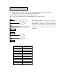
Address list
XC series PLC data register D address is shown as below:
RANGE
SERIES NAME
FOR COMMON
USE
FOR POWER OFF
RETENTIVE USE
FOR SPECIAL USE
D8000~D8029
D8060~D8079
XC1
D
D0~D99
D100~D149
D8120~D8179
D8240~D8249
138
D8306~D8313
D8460~D8469
D8000~D8511
XC2
D
D0~D999
D4000~D4999
XC3
XC5
D
D0~D3999
D4000~D7999
D8000~D9023
1024
XCM
D
D0~D2999
D3000~D4999
D8000~D9023
1024
Structure
D8630~D8729
612
Data register is soft element which used to store data, it includes 16 bits and
32 bits. ( 32 bits contains two registers, the highest bit is sign bit )
16 bits register range is -32,768 ~ +32,767
D0( 16 bits)
0 1 0 0 0 0 1 0 0 1 1 0 0 0 0 0
16 bits
b15
b0
Sign bit
0:positive
1:negative
Use the applied instruction to read and write the register data. Or use other
devices such as HMI.
32 bits value is consisted of two registers. The range is -2147483648 ~ 2147483647.
D 1( 16 bits )
High
32 bits
bit
D 0 (16 bits )
0 1 0 0 0 0 1 0 0 1 1 0 0 0 0 0 0 1 0 0 0 0 1 0 0 1 1 0 0 0 0 0
b31
Sign bit
0: positive
1: negative
When appoint the 32bits register, if set D0, the PLC will connect the next register D1 as
the high bits. Generally, we often appoint even address register.
Function
l
l
Normal type
Ø When write a new value in the register, the former value will be covered.
Ø When PLC from RUN to STOP or STOP to RUN, the value in the register will be
cleared.
Retentive type
Low
bit
b0
l
l
Ø When PLC from RUN to STOP or power off, the value in the register will be retained.
Ø The retentive register range can be set by user.
Special type
Ø Special register is used to set special data, or occupied by the system.
Ø Some special registers are initialized when PLC is power on.
Ø Please refer to the appendix for the special register address and function.
Used as offset (indirect appoint)
Ø Data register can be used as offset of soft element.
Ø Format : Dn[Dm]、Xn[Dm]、Yn[Dm]、Mn[Dm].
Ø Word offset: DXn[Dm] means DX[n+Dm].
Ø The offset value only can be set as D register.
M8002
M2
M8000
MOV
K0
D0
MOV
K5
D0
MOV
D10[D0]
D100
Y0[D0]
When D0=0, D100=D10, Y0 is ON;
When M2 is from OFF→ON, D0=5, D100=D15, Y5 is ON.
D10[D0]=D[10+D0], Y0[D0]=Y[0+D0].
Example
l
Data storage
M0
M1
l
When M0 is ON, write 100 into D0.(16 bits value)
MOV
K100
D0
DMOV
K41100
D10
When M1 is ON, write 41100 into D11,D10 (32bits value)
Data transfer
M0
l
Data register D can deal with many kinds of data and realize various controls.
MOV
D0
D10
When M0 is ON, transfer the value of D10 to D0
Read the timer and counter
M0
MOV
C10
D0
When M0 is ON, move the value of C10 to D0.
l
As the set value of timer and counter
X0
X1
↑
T10
D0
C300
D1
When X0 is ON, T10 starts to work, the time is set in D0.
When X1 is ON once, C300 increase 1, when C300 value=D1,
C300 coil outputs.
2-10.Constant
Data process
XC series PLC use the following 5 number systems.
l
DEC: DECIMAL NUMBER
Ø The preset number of counter and timer ( constant K)
Ø The number of Auxiliary relay M, timer T, counter C, state S.
Ø Set as the operand value and action of applied instruction (constant K)
l
HEX: HEXADECIMAL NUMBER
Ø Set as the operand value and action of applied instruction (constant K)
l
BIN: BINARY NUMBER
Ø Inside the PLC, all the numbers will be processed by binary. But when monitoring on
the device, all the binary will be transformed into HEX or DEC.
l
OCT: OCTAL NUMBER
Ø XC series PLC I/O relays are addressed in OCT. Such as [0-7, 10-17,….70-77,100-107].
l
BCD: BINARY CODE DECIMAL
Ø BCD uses 4 bits binary number to display decimal number 0-9. BCD can be used in 7
segments LED and BCD output digital switch
l
Other numbers ( float number)
XC series PLC can calculate high precision float numbers. It is calculated by binary
numbers, and display by decimal numbers.
PLC program should use K, H to process values. K means decimal
numbers, H means hex numbers. Please note the PLC input/output relay use
octal address.
Display
l Constant K
K is used to display decimal numbers. K10 means decimal number 10. It is used to set timer and
counter value, operand value of applied instruction.
l Constant H
H is used to display hex numbers. H10 means hex number 10. It is used to set operand value of
applied instruction.
2-11.PROGRAM PRINCIPLE
l
Tag P、I
Tag P、I are used in branch division and interruption.
Tag for branch (P) is used in condition jump or subroutine’s jump target;
Tag for interruption (I) is used to specify the e input interruption, time interruption;
The tags P、I are both in decimal form, each coding principle is listed below:
SERIES
NAME
RANGE
XC1、XC2、XC3、XC5、XCM
P
P0~P9999
RANGE
FOR EXTERNAL
INTERRUPTION
SERIES NAME
Input Rising edge
terminals interruption
XC2
I
Falling
edge
interruption
X2
I0000
I0001
X5
I0100
I0101
X10
I0200
I0201
For time interruption
There are 10 channels time interruption,
the represent method is: I40**~I49**.
(“**” represents interruption time, the unit
is mm)
RANGE
FOR EXTERNAL
INTERRUPTION
SERIES NAME I/O
Input
terminals
14
XC3
I
24
32
19
48
60
For time interruption
Rising
Falling
edge
edge
interruption interruption
X7
I0000
I0001
X2
I0000
I0001
X5
I0100
I0101
X10
I0200
I0201
X10
I0000
I0001
X7
I0100
I0101
X6
I0200
I0201
There are 10 channels time interruption,
the represent method is: I40**~I49**.
(“**” represents interruption time, the
unit is mm)
RANGE
FOR EXTERNAL
INTERRUPTION
SERIES NAME I/O
Input
terminals
24
32
XC5
I
48
60
For time interruption
Rising
Falling
edge
edge
interruption interruption
X2
I0000
I0001
X5
I0100
I0101
X10
I0200
I0201
X11
I0300
I0301
X12
I0400
I0401
X2
I0000
I0001
X5
I0100
I0101
X10
I0200
I0201
There are 10 channels time interruption,
the represent method is: I40**~I49**.
(“**” represents interruption time, the
unit is mm)
RANGE
FOR EXTERNAL
INTERRUPTION
SERIES NAME I/O
Input
terminals
XCM
I
24
32
Rising
Falling
edge
edge
interruption interruption
X2
I0000
I0001
X5
I0100
I0101
For time interruption
There are 10 channels time interruption,
the represent method is: I40**~I49**.
X10
I0200
I0201
X11
I0300
I0301
X12
I0400
I0401
(“**” represents interruption time, the
unit is mm)
Tag P is usually used in flow, it is used with CJ (condition jump)、CALL (subroutine
call)etc.
l Condition Jump CJ
X0
CJ
P1
If coil X0 gets ON, jump to the step behind
tag P1;
If the coil X0 is not ON, do not execute
jump action, but run with the original
program;
X1
Y0
P1
X2
RST
T0
Tag P
l Call the subroutine (CALL)
X0
If X0 gets ON, jump to the
subroutine from the main program;
If the coil is not ON, run with the
original program;
Subroutine
FEND
P10
Main program
CALL
After executing the subroutine,
return to the main program;
P10
SRET
Tag I
Tag I is usually used in interruption, including external interruption, time interruption etc.
use with IRET (interruption return)、EI (enable interruption)、DI (disable interruption);
l External interruption
Ø Accept the input signal from the special input terminals, not effected by the scan
cycle. Activate the input signal, execute the interruption subroutine.
Ø With external interruption, PLC can dispose the signal shorter than scan cycle;
So it can be used as essential priority disposal in sequence control, or used in
short time pulse control.
l Time interruption
Ø Execute the interruption subroutine at each specified interruption loop tine. Use
this interruption in the control which requires it to be different with PLC’s
operation cycle;
l
Action order of input/output relays and response delay
Ø Input disposal
Before PLC executing the program, read all the input terminal’s ON/OFF status of PLC
to the image area. In the process of executing the program, even the input changed, the
content in the input image area will not change. However, in the input disposal of next
scan cycle, read out the change.
Ø Output disposal
Once finish executing all the instructions, transfer the ON/OFF status of output Y image
area to the output lock memory area. This will be the actual output of the PLC. The
contacts used for the PLC’s exterior output will act according to the device’s response
delay time.
When use this input/output format in a batch, the drive time and operation cycle of input filter
and output device will also appear response delay.
l Not accept narrow input pulse signal
PLC’s input ON/OFF time should be longer than its loop time. If consider input filter’s response
delay 10ms, loop time is 10ms,then ON/OFF time needs 20 ms separately. So, up to 1,
000/(20+20)=25Hz input pulse can’t be disposed. But, this condition could be improved when use
PLC’s special function and applied instructions.
l
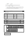
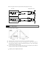
Dual output(Dual coils)action
X1
Y3
X2
Y3
Y4
Y3
When executing dual output (use dual coil),
the back side act in prior.
As shown in the left map, please consider
the things of using the same coil Y003 at
many positions:
E.g. X001=ON,X002=OFF
At first, X001 is ON, its image area is ON,
output Y004 is also ON.
But, as input X002 is OFF, the image area
of Y003 is OFF.
So, the actual output is: Y003=OFF,
Y004= ON.
3
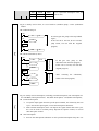
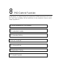
Basic Program Instructions
In this chapter, we tell the basic instructions and their functions.
3-1.Basic Instructions List
3-2.[LD], [LDI], [OUT]
3-3.[AND], [ANI]
3-4.[OR], [ORI]
3-5.[LDP], [LDF], [ANDP], [ANDF], [ORP], [ORF]
3-6.[LDD], [LDDI]
3-7.[ORB]
3-8.[ANB]
3-9.[MCS], [MCR]
3-10.[ALT]
3-11.[PLS], [PLF]
3-12.[SET], [RST]
3-13.[OUT], [RST] (Aim at counter device)
3-14.[NOP], [END]
3-15.[GROUP], [GROUPE]
3-16.Items to be attended when programming
3-1.Basic Instructions List
All XC1、XC2、XC3、XC5、XCM series support the below instructions:
Mnemonic
Function
LD
(LoaD)
Initial logical operation
contact type NO (normally
open)
Format and Device
Chapter
3-2
X、Y、M、S、T、C、Dn.m、FDn.m
LDD
(LoaD
Directly)
Read the status from the
contact directly
3-6
X0
D
X
LDI
(LoaD
Inverse)
Initial logical operation
contact type NC (normally
closed)
3-2
X、Y、M、S、T、C、Dn.m、FDn.m
LDDI
Read the normally closed
contact directly
3-6
X0
D
X
LDP
(LoaD
Pulse)
Initial logical
operation-Rising edge
pulse
3-5
X、Y、M、S、T、C、Dn.m、FDn.m
LDF
(LoaD
Falling
Pulse)
Initial logical
operation-Falling /trailing
edge pulse
AND
(AND)
Serial connection of NO
(normally open) contacts
3-5
X、Y、M、S、T、C、Dn.m、FDn.m
3-3
M0
X、Y、M、S、T、C、Dn.m、FDn.m
ANDD
Read the status from the
contact directly
X0
3-6
D
X
ANI
(AND
Inverse)
Serial connection of NC
(normally closed) contacts
3-3
M0
X、Y、M、S、T、C、Dn.m、FDn.m
ANDDI
Read the normally closed
contact directly
X0
D
X
3-6
ANDP
(AND
Pulse)
Serial connection of rising
edge pulse
3-5
X、Y、M、S、T、C、Dn.m、FDn.m
ANDF
(AND
Falling
pulse)
Serial connection of
falling/trailing edge pulse
OR
(OR)
Parallel connection of NO
(normally open) contacts
3-5
X、Y、M、S、T、C、Dn.m、FDn.m
3-4
X、Y、M、S、T、C、Dn.m、FDn.m
ORD
3-6
Read the status from the
contact directly
X0
D
X
ORI
(OR
Inverse)
Parallel connection of NC
(normally closed) contacts
3-4
X、Y、M、S、T、C、Dn.m、FDn.m
ORDI
Read the normally closed
contact directly
3-6
X0
D
X
ORP
(OR
Pulse)
Parallel connection of
rising edge pulse
3-5
X、Y、M、S、T、C、Dn.m、FDn.m
ORF
(OR
Falling
pulse)
Parallel connection of
falling/trailing edge pulse
ANB
(ANd
Block)
Serial connection of
multiply parallel circuits
3-5
X、Y、M、S、T、C、Dn.m、FDn.m
3-8
None
ORB
(OR
Block)
Parallel connection of
multiply parallel circuits
3-7
None
OUT
(OUT)
Final logic operation type
coil drive
3-2
Y、M、S、T、C、Dn.m
OUTD
Output to
directly
the
contact
Y0
D
3-6
Y
SET
(SET)
Set a bit device
permanently ON
3-12
Y、M、S、T、C、Dn.m
RST
(ReSeT)
3-12
Reset a bit device
permanently OFF
Y、M、S、T、C、Dn.m
PLS
(PuLSe)
3-11
Rising edge pulse
X、Y、M、S、T、C、Dn.m
PLF
(PuLse
Falling)
Falling/trailing edge pulse
3-11
X、Y、M、S、T、C、Dn.m
MCS
(New bus
line start)
Connect the public serial
contacts
Y0
3-9
Y0
3-9
None
MCR
(Bus line
return)
Clear the public serial
contacts
None
ALT
(Alternate
state)
The status of the assigned
device is inverted on every
operation of the instruction
END
(END)
Force the current program
scan to end
ALT
M0
3-10
X、Y、M、S、T、C、Dn.m
3-14
None
GROUP
Group
3-15
None
GROUPE
Group End
3-15
None
TMR
Time
2-7
3-2.[LD] , [LDI] , [OUT]
Mnemonic and Function
Mnemonic
LD
(LoaD)
Function
Initial logic operation
contact
type
NO
(Normally Open)
Format and Operands
Operands: X、Y、M、S、T、C、
Dn.m、FDn.m
LDI
(LoaD Inverse)
Initial logic operation
contact
type
NC
(Normally Closed)
Devices:X、Y、M、S、T、C、Dn.m、
FDn.m
OUT
(OUT)
Final logic operation
type drive coil
Operands: X、Y、M、S、T、C、
Dn.m
Statement
l
l
l
l
l
Connect the LD and LDI instructions directly to the left bus bar. Or use them
to define a new block of program when using ANB instruction.
OUT instruction is the coil drive instruction for the output relays、auxiliary
relays、status、timers、counters. But this instruction can’t be used for the
input relays
Can not sequentially use parallel OUT command for many times.
For the timer’s time coil or counter’s count coil, after using OUT instruction,
set constant K is necessary.
For the constant K’s setting range、actual timer constant、program’s step
relative to OUT instruction (include the setting value), See table below:
Timer, Counter
Setting Range of constant K
1ms Timer
10ms Timer
0.001~32.767 sec
1~32,767
100ms Timer
16 bits counter
The actual setting value
0.01~327.67 sec
0.1~3276.7 sec
1~32,767
Same as the left
32 bits counter
Program
1~2,147,483,647
Same as the left
X0
Y100
X1
M1203
T0
T0
Y1
K19
LD
OUT
LDI
OUT
OUT
LD
OUT
X0
Y100
X1
M1203
T0
T0
Y1
K19
3-3.[AND] , [ANI]
Mnemonic and Function
Mnemonic
AND
(AND)
Function
Serial connection of
NO
(Normally
Open) contacts
Format and Operands
M0
Operands: X、Y、M、S、T、C、Dn.m、FDn.m
ANI
(ANd
Inverse)
Serial connection of
NC
(Normally
Closed) contacts
M0
Operands: X、Y、M、S、T、C、Dn.m、FDn.m
Statements
l
l
Use the AND and the ANI instruction for serial connection of contacts. As
many contacts as required can be connected in series. They can be used for
many times.
The output processing to a coil, through writing the initial OUT instruction is
called a “follow-on” output (For an example see the program below: OUT M2
and OUT Y003). Follow-on outputs are permitted repeatedly as long as the
output order is correct. There’s no limit for the serial connected contacts’ Nr.
and follow-on outputs’ number.
X2 M1
Program
Y2
Y2 X3
M2
T1
Y3
LD
AND
OUT
LD
ANI
OUT
AND
OUT
X2
M1
Y2
Y2
X3
M2
T1
Y3
3-4.[OR] , [ORI]
Mnemonic and Function
Mnemonic
OR
(OR)
Function
Parallel connection
of NO (Normally
Open) contacts
Format and Operands
Operands: X、Y、M、S、T、C、Dn.m、FDn.m
ORI
(OR
Inverse)
Parallel connection
of NC (Normally
Closed) contacts
Operands: X、Y、M、S、T、C、Dn.m、FDn.m
Statements
l
l
Use the OR and ORI instructions for parallel connection of contacts. To connect a block
that contains more than one contact connected in series to another circuit block in parallel,
use an ORB instruction, which will be described later;
OR and ORI start from the instruction’s step, parallel connect with the LD and LDI
instruction’s step said before. There is no limit for the parallel connect times.
X5
X6
Program
Y6
M11
Y6 M4 X7
M12
M13
M100
LD
OR
OR
OUT
LDI
AND
OR
ANI
OR
OUT
X5
X6
M11
Y6
Y6
M4
M12
X7
M13
M100
Relationship with ANB
The parallel connection with OR, ORI
instructions should connect with LD, LDI
instructions in principle. But behind the
ANB instruction, it’s still ok to add a LD
or LDI instruction.
3-5.[LDP] , [LDF] , [ANDP] , [ANDF] , [ORP] , [ORF]
Mnemonic and Function
Mnemonic
LDP
(LoaD
Pulse)
Function
Initial
operation-Rising
pulse
Format and Operands
logical
edge
Operands: X、Y、M、S、T、C、Dn.m、FDn.m
LDF
(LoaD
Falling
pulse)
ANDP
(AND
Pulse)
Initial logical operation
Falling/trailing edge pulse
Operands: X、Y、M、S、T、C、Dn.m、FDn.m
Serial
connection
Rising edge pulse
of
Operands: X、Y、M、S、T、C、Dn.m、FDn.m
ANDF
(AND
Falling
pulse)
ORP
(OR
Pulse)
Serial
connection
of
Falling/trailing edge pulse
Operands: X、Y、M、S、T、C、Dn.m、FDn.m
Parallel connection
Rising edge pulse
of
Operands: X、Y、M、S、T、C、Dn.m、FDn.m
ORF
(OR
Falling
pulse)
Parallel connection of
Falling/trailing edge pulse
Operands: X、Y、M、S、T、C、Dn.m、FDn.m
Statements
l
l
LDP、ANDP、ORP are active for one program scan after the associated devices switch from
OFF to ON.
LDF、ANDF、ORF are active for one program scan after the associated devices switch from
ON to OFF.
X5
Program
M13
X6
M8000 X7
M15
LDP
ORP
OUT
LD
ANDP
OUT
X5
X6
M13
M8000
X7
M15
3-6.[LDD] , [LDDI] , [ANDD] , [ANDDI] , [ORD] , [ORDI],[OUTD]
Mnemonic and Function
Mnemonic
Function
Format and Operands
LDD
Read the status from the
X0
contact directly
D
Devices: X
LDDI
Read the normally closed
X0
contact directly
D
Devices: X
ANDD
Read the status from the
contact directly
X0
D
Devices: X
ANDDI
Read
the
normally
closed contact directly
X0
D
Devices: X
ORD
Read the status from the
contact directly
X0
D
Devices: X
Read
the
normally
closed contact directly
ORDI
X0
D
Devices: X
Output to the contact
directly
OUTD
Y0
D
Devices: Y
Statements
l
l
The function of LDD、ANDD、ORD instructions are similar with LD、AND、OR; LDDI、
ANDDI、ORDI instructions are similar with LDI、ANDI、ORI; but if the operand is X, the
LDD、ANDD、ORD commands read the signal from the terminals directly, this is the only
difference.
OUTD and OUT are output instructions. But if use OUTD, output immediately if the
condition comes true, needn't wait the next scan cycle.
X0
Program
D
X2
D
Y0
D
M13
X1
D
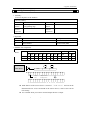
3-7.[ORB]
Mnemonic and Function
Mnemonic
Function
Format and Devices
ORB
(OR Block)
Parallel connection
of multiply parallel
circuits
Devices: none
LDD
LDDI
ORD
ANB
OUTD
X0
X2
X2
Y0
Statements
l
l
l
The serial connection with two or more contacts is called "serial block". If parallel connect
the serial block, use LD, LDI at the branch start place, use ORB at the stop place;
As the ANB instruction,an ORB instruction is an independent instruction and is not
associated with any device number.
There are no limitations to the number of parallel circuits when using an ORB instruction in
the sequential processing configuration.
Program
Recommended
good
programming method:
LD
AND
LD
AND
ORB
LD
AND
ORB
X0
X1
X2
X3
X4
X5
Non-preferred batch
programming
method:
LD
X0
AND
X1
LD
X2
AND
X3
LD
X4
AND
X5
ORB
ORB
3-8.[ANB]
Mnemonic and Function
Mnemonic
Function
ANB
(And
Block)
Serial
connection of
multiply
parallel circuits
l
Statements
l
Format and Devices
Devices: none
To declare the starting point of the circuit block, use a LD or LDI
instruction. After completing the parallel circuit block, connect it to the
preceding block in series using the ANB instruction.
It is possible to use as many ANB instructions as necessary to connect a
number of parallel circuit blocks to the preceding block in series.
Program
LD
OR
LD
AND
LDI
AND
ORB
OR
ANB
OR
OUT
X0
X1
X2
X3
X4
X5
Start of a branch
End of a parallel circuit block
X6
X7
Y20
Serial connect with the preceding circuit
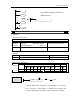
3-9.[MCS] , [MCR]
Mnemonic and Function
Mnemonic
Function
MCS
(Master
control)
Denotes
the
start
of
a
master control
block
l
l
l
l
Devices:None
Y0
Devices:None
After the execution of an MCS instruction, the bus line(LD、LDI)shifts
to a point after the MCS instruction. An MCR instruction returns this to
the original bus line.
MCS、MCR instructions should use in pair.
The bus line could be used nesting. Between the matched MCS、MCR
instructions use matched MCS、MCR instructions. The nest level
increase with the using of MCS instruction. The max nest level is 10.
When executing MCR instruction, go back to the upper bus line.
When use flow program, bus line management could only be used in the
same flow. When end some flow, it must go back to the main bus line.
X1
Program
Y0
Denotes
the
end of a master
control block
MCR
(Master
control
Reset)
Statements
Format and Devices
LD
X2
M1
Y0
M3
M2
Y1
Y2
X1
MCS
Bus line starts
LD
X2
OUT
Y0
LD
M1
MCS
Bus line nest
LD
M3
OUT
Y1
LD
M2
OUT
Y2
MCR
MCR
Bus line back
3-10.[ALT]
Mnemonic and Function
Mnemonic
ALT
(Alternate
status)
Statements
Function
Format and Devices
The status of the
assigned
devices
inverted on every
operation of the
instruction
ALT
M0
Devices: Y、M、S、T、C、Dn.m
The status of the destination device is alternated on every operation of the
ALT instruction.
M100
ALT
Program
M0
M0
Y0
M0
Y1
LDP
ALT
LD
OUT
LDI
OUT
M100
M0
M0
Y0
M0
Y1
3-11.[PLS] , [PLF]
Mnemonic and Function
Mnemonic
PLS
(Pulse)
Function
Rising
pulse
Format and Devices
edge
Devices: Y、M、S、T、C、Dn.m
PLF
(Pulse
Falling)
Falling/trailing
edge pulse
Devices: Y、M、S、T、C、Dn.m
Statements
l
l
When a PLS instruction is executed, object devices Y and M operate
for one operation cycle after the drive input signal has turned ON.
When a PLF instruction is executed, object devices Y and M operate
for one operation cycle after the drive input signal has turned OFF.
X0
Program
M0
X1
PLS
M0
SET
Y0
PLF
M1
RST
Y0
M1
LD
X0
PLS
M0
LD
M0
SET
Y0
---------------------LD
X1
PLF
M1
LD
M1
RST
Y0
3-12.[SET] , [RST]
Mnemonic and Function
Mnemonic
SET(Set)
Function
Format and Devices
Set a bit device
permanently
ON
Devices: Y、M、S、T、C、Dn.m
RST(Reset)
Reset a bit
device
permanently
OFF
Devices: Y、M、S、T、C、Dn.m
Statements
l
Turning ON X010 causes Y000 to turn ON. Y000 remains ON even after
X010 turns OFF. Turning ON X011 causes Y000 to turn OFF. Y000
remains OFF even after X011 turns OFF. It’s the same with M、S.
SET and RST instructions can be used for the same device as many times
as necessary. However, the last instruction activated determines the
current status.
Besides, it’s also possible to use RST instruction to reset the current
contents of timer, counter and contacts.
When use SET, RST commands, avoid to use the same ID with OUT
command;
l
l
l
X10
Program
SET
Y0
RST
Y0
SET
M50
RST
M50
SET
S0
RST
S0
X11
X12
X13
X14
X15
X10
X17
X10
X11
Y0
T250
RST
T250
K10
LD
SET
LD
RST
LD
SET
LD
RST
LD
SET
LD
RST
LD
OUT
LD
RST
X10
Y0
X11
Y0
X12
M50
X13
M50
X14
S0
X15
S0
X10
T250
X17
T250
K10
3-13.【OUT】,【RST】for the counters
Mnemonic and Function
Mnemonic
OUT
Function
Format and Devices
Final
logic
operation
type
coil drive
RST
Device:K、D
Reset a bit device
permanently OFF
Device:C
Programming of
interior counter
Counter used for power cut retentive.
Even when power is cut, hold the current
value and output contact’s action status
and reset status.
C0 carries on increase count for the
OFF→ON of X011. When reach the
set value K10, output contact C0
activates. Afterwards, even X011 turns
from OFF to ON, counter’s current
value will not change, output contact
keep on activating.
To clear this, let X010 be the activate
status and reset the output contact. It’s
necessary to assign constant K or
indirect data register’s ID behind OUT
instruction.
Programmi
ng of high
speed
l
l
l
In the preceding example, when M0 is ON, carry on positive count with OFF→ON
of X0.
Counter’s current value increase, when reach the set value (K or D), the output
contact is reset.
When M1 is ON, counter’s C600 output contact is reset, counter’s current value turns
to be 0.
3-14. [END]
Mnemonic and Function
Mnemonic
END
(END)
Statements
Function
Force
the
current
program scan
to end
Format and Devices:None
Devices: None
PLC repeatedly carry on input disposal, program
executing and output disposal. If write END
instruction at the end of the program, then the
instructions behind END instruction won’t be
executed. If there’s no END instruction in the
program, the PLC executes the end step and then
repeat executing the program from step 0.
When debug, insert END in each program
segment to check out each program’s action.
Then, after confirm the correction of preceding
block’s action, delete END instruction.
Besides, the first execution of RUN begins with
END instruction.
When executing END instruction, refresh monitor timer. (Check if scan cycle is a long timer.)
3-15.[GROUP] , [GROUPE]
Mnemonic and Function
Mnemonic
GROUP
Function
Format and Device
GROUP
Devices: None
GROUPE
GROUP END
Devices: None
Statements
l
l
l
GROUP and GROUPE should used in pairs.
GROUP and GROUPE don't have practical meaning, they are used to optimize the program
structure. So, add or delete these instructions doesn't effect the program's running;
The using method of GROUP and GROUPE is similar with flow instructions; enter GROUP
instruction at the beginning of group part; enter GROUPE instruction at the end of group
part.
Generally,
GROUP
and
GROUPE
instruction can be programmed according to
the group's function. Meantime, the
programmed instructions can be FOLDED or
UNFOLDED. To a redundant project, these
two instructions are quite useful.
3-16.Items To Note When Programming
1、Contacts’ structure and step number
Even in the sequencial control circuit with the same action, it’s also available to
simple the program and save program’s steps according to the contacts’ structure.
General program principle is:a)write the circuit with many serial contacts on the top;
b)write the circuit with many parallel contacts in the left.
2、Program’s executing sequence
Handle the sequencial control program by【From top to bottom】and【From left to
right】
Sequencial control instructions also encode following this flow.
3、Dual output dual coil’s activation and the solution
l If carry on coil’s dual output (dual coil) in the sequencial control program, then
the backward action is prior.
l Dual output (dual coil) doesn’t go against the input rule at the program side. But
as the preceding action is very complicate, please modify the program as in the
following example.
X0
X3
X2
X4
Y0
X0
X2
X3
X4
X0
X2
X3
X4
Y0
Y0
M0
M0
M1
Y0
M1
There are other methods. E.g. jump instructions or step ladder. However, when use
step ladder, if the main program’s output coil is programmed, then the disposal
method is the same with dual coil, please note this.
4 applied instructions
4
Applied Instructions
In this chapter, we describe applied instruction’s function of XC series PLC.
4-1.Table of Applied Instructions
4-2.Reading Method of Applied Instructions
4-3.Flow Instructions
4-4.Contactors Compare Instructions
4-5.Move Instructions
4-6.Arithmetic and Logic Operation Instructions
4-7.Loop and Shift Instructions
4-8.Data Convert
4-9.Floating Operation
4-10.Clock Operation
4 applied instructions
4 applied instructions
4-1.Applied Instruction List
Mnemonic
Function
Ladder chart
Chapter
Program Flow
CJ
Condition jump
CJ
Pn
4-3-1
CALL
Call subroutine
CALL
Pn
4-3-2
SRET
Subroutine return
SRET
4-3-2
STL
Flow start
STLE
Flow end
SET
Open the assigned flow, close
the current flow
S
Open the assigned flow, not
close the current flow
D
·
4-3-3
Start a FOR-NEXT loop
D
·
4-3-4
ST
FOR
End of a FOR-NEXT loop
NEXT
FEND
Main program END
END
Program END
STL Sn
4-3-3
S 1 ·
4-3-3
·
4-3-3
D
·
4-3-4
D
·
4-3-5
4-3-5
Data Compare
LD=
LD activates if (S1) = (S2)
LD>
LD activates if (S1) > (S2)
LD<
LD activates if (S1) =< (S2)
LD<>
LD activates if(S1)≠(S2)
LD<=
LD activates if(S1)≤(S2)
LD>=
LD activates if(S1)≥(S2)
AND=
AND activates if(S1)=(S2)
S
·
4-4-1
D
·
4-4-1
D
·
4-4-1
D
·
4-4-1
D
·
4-4-1
LD>=
S1
AND=
4-4-1
S2
S1
S2
4-4-2
4 applied instructions
AND>
AND activates if(S1)>(S2)
AND<
AND activates if(S1)<(S2)
AND<>
AND activates if(S1)≠(S2)
AND<=
AND activates if(S1)≤(S2)
AND>=
AND activates if(S1)≥(S2)
X 1
X 2
OR=
OR activates if(S1)=(S2)
OR>
OR activates if(S1)>(S2)
OR<
OR activates if(S1)<(S2)
OR<>
OR activates if(S1)≠(S2)
OR<=
OR activates if(S1)≤(S2)
AND>
S1
S2
4-4-2
AND<
S1
S2
4-4-2
AND<>
S1
S2
4-4-2
AND<=
S1
S2
4-4-2
B M
O
V
D 1 0
D 9
K 3
B M
O
V
D 1 0
D 1 1
K 3
OR=
X0
S1
PMOV
S·
D·
n
D5
D10
K3
4-4-3
S1
S2
4-4-3
OR<>
S1
S2
4-4-3
X
0
OR activates if(S1)≥(S2)
4-4-3
S2
OR<
DFMOV
OR>=
4-4-2
S·
D·
n
D0
D10
K3
S1
OR>=
4-4-3
4-4-3
S2
Data Move
CMP
Compare the data
ZCP
Compare the data in certain area
S1
CMP
S
S·
MOV
BMOV
PMOV
X 2
FW R T
Move
Block move
MOV
X0
Transfer the Data block
D 1·
D 0
4-5-1
D 2·
FD 0
S
MSET
D
K 3
D
4-5-2
4-5-3
D 1·
D 2·
M 10
M 120
4-5-4
D
2
·
4-5-5
D
1
·
4-5-6
FMOV
Multi-points repeat move
FWRT
Flash ROM written
D
2
·
4-5-7
MSET
Zone set
D
1
·
4-5-8
ZRST
Zone reset
D
2
·
4-5-9
SWAP
Swap the high and low byte
D
1 ·
4-5-10
4 applied instructions
D
X
XCH
0
Exchange two values
Z R
S
T
Z R
S
T
M
1
·
D
5 0 0
D
D
1
M
2 ·
5 5 9
·
D
0
D
4-5-11
2 ·
1 0 0
Data Operation
ADD
Addition
D
2
·
4-6-1
SUB
Subtraction
D
1
·
4-6-2
MUL
Multiplication
D
2
·
4-6-3
DIV
Division
D
1
·
4-6-4
INC
Increment
D
1 ·
4-6-5
DEC
Decrement
D
2 ·
4-6-5
D
MEAN
Mean
WAND
Word And
WAND
WOR
Word OR
WOR
WXOR
Word exclusive OR
CML
Compliment
NEG
Negative
1
·
S1
CML
S2
D
4-6-7
S2
D
4-6-7
S1 S2
D
4-6-7
S1
WXOR
4-6-6
S
D
4-6-8
4-6-9
Data Shift
SHL
Arithmetic Shift Left
SHL
D
n
4-7-1
SHR
Arithmetic Shift Right
SHR
D
n
4-7-1
LSL
Logic shift left
4-7-2
LSR
Logic shift right
4-7-2
ROL
Rotation shift left
4-7-3
ROR
Rotation shift right
4-7-3
SFTL
Bit shift left
SFTL
S
D
n1
n2
4-7-4
4 applied instructions
SFTR
S
D
n1
n2
SFTR
Bit shift right
WSFL
Word shift left
4-7-6
WSFR
Word shift right
4-7-7
4-7-5
Data Convert
WTD
Single word integer converts
to double word integer
FLT
16 bits integer converts to
float point
4-8-2
DFLT
32 bits integer converts to
float point
4-8-2
FLTD
64 bits integer converts to
float point
4-8-2
INT
Float point converts to integer
4-8-3
BIN
BCD converts to binary
4-8-4
BCD
Binary converts to BCD
4-8-5
ASCI
Hex. converts to ASCII
HEX
ASCII converts to Hex.
4-8-7
DECO
Coding
4-8-8
ENCO
High bit coding
4-8-9
ENCOL
WTD
ASCI
S
S
D
D
4-8-1
n
4-8-6
Low bit coding
4-8-10
Float Point Operation
ECMP
S1
S2
D
ECMP
Float compare
EZCP
Float Zone compare
EADD
Float Add
4-9-3
ESUB
Float Subtract
4-9-4
EZCP
S1
S2
D1
4-9-1
D2
4-9-2
4 applied instructions
EMUL
Float Multiplication
4-9-5
EDIV
Float division
4-9-6
ESQR
Float Square Root
4-9-7
SIN
Sine
4-9-8
COS
Cosine
4-9-9
TAN
Tangent
4-9-10
ASIN
Floating Sine
4-9-11
ACOS
Floating Cosine
4-9-12
ATAN
Floating Tangent
4-9-13
Clock Operation
TRD
Read RTC data
4-10-1
TWR
Write RTC data
4-10-2
4 applied instructions
4-2.Reading Method of Applied Instructions
In this manual, the applied instructions are described in the following manner.
1.Summary
ADDITION [ADD]
16 bits
ADD
32 bits
DADD
Execution
Normally ON/OFF, Rising/Falling
Suitable
XC1.XC2.XC3.XC5.XCM
condition
edge
Models
Hardware
-
Software
requirement
-
requirement
2.Operands
Operands
Function
Data Type
S1
Specify the augend data or register
16 bits/32 bits, BIN
S2
Specify the summand data or register
16 bits/32 bits, BIN
D
Specify the register to store the sum
16 bits/32 bits, BIN
3.Suitable Soft Components
Word
Bit
operands
System
D
FD
S1
●
S2
D
ED
Constant
Module
ID
TD
CD
DX
DY
DM
DS
K/H
●
●
●
●
●
●
●
●
●
●
●
●
●
●
●
●
●
●
●
●
●
●
●
●
Operands
QD
System
X
Y
M
S
T
C
Dn.m
<16 bits instruction>
Description
X0
ADD
S1·
S2·
D·
D10
D12
D14
S1·
S2·
D·
D10
D12
D14
(D10)+(D12)→(D14)
<32 bits instruction>
X0
DADD
(D11D10)+(D13D12)→(D15D14)
l
The data contained within the two source devices are combined and total is stored in the specified
4 applied instructions
destination device. Each data’s highest bit is the sign bit, 0 stands for positive, 1 stand for negative. All
calculations are algebraic processed. (5+(-8)= -3).
l
If the result of a calculations is “0”, the “0’ flag acts. If the result exceeds 323,767(16 bits limit) or
2,147,483,648 ( 32 bits limit), the carry flag acts. ( refer to the next page). If the result exceeds -323,768 (16
bits limit) or -2,147,483,648 (32 bits limit ) , the borrow flag acts (Refer to the next page)
l
When carry on 32 bits operation, word device’s 16 bits are assigned, the device follow closely the preceding
device’s ID will be the high bits. To avoid ID repetition, we recommend you assign device’s ID to be even
ID.
l
The same device may be used a source and a destination. If this is the case then the result changes after
every scan cycle. Please note this point.
Related flag
Flag
Name
M8020
Zero
Function
ON:the calculate result is zero
OFF:the calculate result is not zero
ON:the calculate result is over 32767(16bits) or 2147483647(32bits)
M8021
Borrow
OFF:the calculate result is not over 32767(16bits) or 2147483647(32bits)
ON:the calculate result is over 32767(16bits) or 2147483647(32bits)
M8022
Carry
The related
description
OFF:the calculate result is not over 32767(16bits) or 2147483647(32bits)
l
The assignment of the data
The data register of XC series PLC is a single word (16 bit) data
register, single word data only engross one data register which is
assigned by single word object instruction. The disposal bound is: Dec.
–327,68~327,67, Hex. 0000~FFFF.
Single word object instruction
Instruction D(NUM)
D(NUM)
→
Object data
Double word(32 bit)engrosses two data register, it’s composed by two consecutive data
registers, the first one is assigned by double word object instruction. The dispose bound is:
Dec. -214,748,364,8~214,748,364,7, Hex. 00000000~FFFFFFFF.
Double word object instruction
Instruction D(NUM)
l
D(NUM+1)
→
Object data
D(NUM)
Object data
The denote way of 32 bits instruction
If an instruction can not only be 16 bits but also be 32 bits, then the denote method for 32
bits instruction is to add a “D” before 16 bits instruction.
E.g:ADD D0 D2 D4 denotes two 16 bits data adds;
DADD D10 D12 D14 denotes two 32 bits data adds
4 applied instructions
※1:Flag after executing the instruction. Instructions without the direct flag will not display.
※2: S· Source operand, its content won’t change after executing the instruction
※3: D· Destinate operand, its content changes with the execution of the instruction
※4:Tell the instruction’s basic action, using way, applied example, extend function, note items
etc.
4-3.Program Flow Instructions
Mnemonic
Instruction’s name
Chapter
CJ
Condition Jump
4-3-1
CALL
Call subroutine
4-3-2
SRET
Subroutine return
4-3-2
STL
Flow start
4-3-3
STLE
Flow end
4-3-3
SET
Open the assigned flow, close the current flow (flow
jump)
4-3-3
ST
Open the assigned flow, not close the current flow (Open
the new flow)
4-3-3
FOR
Start of a FOR-NEXT loop
4-3-4
NEXT
End of a FOR-NEXT loop
4-3-4
FEND
First End
4-3-5
END
Program End
4-3-5
4 applied instructions
4-3-1.Condition Jump [CJ]
1.Summary
As used to run a part of program, CJ shorten the operation cycle and using the dual coil
Condition Jump [CJ]
16 bits
CJ
32 bits
-
Execution
Normally ON/OFF coil
Suitable
XC1.XC2.XC3.XC5.XCM
condition
Models
-
Hardware
Software
requirement
-
requirement
2.Operands
Operands
Function
Data Type
Pn
Jump to the target (with pointer Nr.) P (P0~P9999)
Pointer's Nr.
3.Suitable Soft Components
Other
Pointer
P
I
●
Description
In the below graph, if X000 is “ON”, jump from the first step to the next step
behind P6 tag. If X000 “OFF”, do not execute the jump construction;
4 applied instructions
X0
CJ
P6
l In the left graph, Y000 becomes to be
dual coil output, but when
X000=OFF, X001 activates; when
X000=ON, X005 activates
l CJ can’t jump from one STL to
another STL;
l After driving time T0~T640 and HSC
C600~C640, if execute CJ, continue
to work, the output activates.
X1
Y0
X2
X3
X4
RST
T246
T246
K1000
MOV
K3
CJ
P7
D0
P6
X0
X5
Y0
P7
X6
RST
T246
4-3-2.Call subroutine [CALL] and Subroutine return [SRET]
1.Summary
Call the programs which need to be executed together, decrease the program's steps;
Subroutine Call [CALL]
16 bits
CALL
32 bits
-
Execution
Suitable
XC1.XC2.XC3.XC5.XCM
condition
Normally ON/OFF,
Rising/Falling edge
Hardware
-
Software
requirement
Models
-
requirement
Subroutine Return [SRET]
16 bits
SRET
32 bits
-
Execution
-
Suitable
XC1.XC2.XC3.XC5.XCM
condition
Hardware
Models
-
requirement
Software
-
requirement
2.Operands
Operands
Function
Data Type
Pn
Jump to the target (with pointer Nr.) P (P0~P9999)
Pointer's Nr.
3.Suitable Soft Components
4 applied instructions
Others
Pointer
P
I
●
X0
P10
Main Program
CALL
Description
l If X000= “ON”, execute
the call instruction and
jump to the step tagged by
P10. after executing the
subroutine,
return the
original step via SRET
instruction.Program the tag
with FEND instruction
(will
describe
this
instruction later)
l In the subroutine 9 times
call is allowed, so totally
there can be 10 nestings.
FEND
P10
Subroutine
SRET
END
4-3-3.Flow [SET].[ST] .[STL]. [STLE]
1、Summary
Instructions to specify the start, end, open, close of a flow;
Open the specified flow, close the local flow [SET]
16 bits
SET
32 bits
-
Execution
Suitable
XC1.XC2.XC3.XC5.XCM
condition
Normally ON/OFF,
Rising/Falling edge
Hardware
-
Software
Models
requirement
-
requirement
Open the specified flow, not close the local flow [ST]
16 bits
ST
Execution
condition
Normally
Rising/Falling edge
Hardware
-
requirement
ON/OFF,
32 bits
-
Suitable
XC1.XC2.XC3.XC5.XCM
Models
Software
-
requirement
Flow starts [STL]
16 bits
STL
32 bits
-
4 applied instructions
Execution
-
XC1.XC2.XC3.XC5.XCM
Suitable
condition
Models
Hardware
-
-
Software
requirement
requirement
Flow ends [STLE]
16 bits
STLE
32 bits
-
Execution
-
Suitable
XC1.XC2.XC3.XC5.XCM
condition
Models
Hardware
-
-
Software
requirement
requirement
2.operands
Operands
Function
Data Type
Sn
Jump to the target flow S
Flow ID
3.Suitable Soft Components
Bit
System
Operands
X
Sn
Y
M
S
T
C
Dn.m
●
Description
l
l
l
l
l
l
l
l
STL and STLE should be used in pairs. STL represents the start of a flow, STLE represents
the end of a flow.
After executing of SET Sxxx instruction, the flow specified by these instructions is ON.
After executing RST Sxxx instruction, the specified flow is OFF.
In flow S0, SET S1 close the current flow S0, open flow S1.
In flow S0, ST S2 open the flow S2, but don’t close flow S0.
When flow turns from ON to be OFF, reset OUT、PLS、PLF、not accumulate timer etc.
which belongs to the flow.
ST instruction is usually used when a program needs to run more flows at the same time.
After executing of SET Sxxx instruction, the pulse instructions will be closed (including
one-segment, multi-segment, relative or absolute, return to the origin)
4 applied instructions
SET
S0
SET
S1
ST
S2
STL S0
STLE
STL S1
STLE
STL S2
STLE
4 applied instructions
4-3-4. [FOR] and [NEXT]
1.Summary
Loop execute the program between FOR and NEXT with the specified times;
Loop starts [FOR]
16 bits
FOR
32 bits
-
Execution
Rising/Falling edge
Suitable
XC1.XC2.XC3.XC5.XCM
condition
Models
-
Hardware
Software
requirement
-
requirement
Loop ends [NEXT]
16 bits
NEXTs
32 bits
-
Execution
Normally ON/OFF,
Rising/Falling edge
Suitable
XC1.XC2.XC3.XC5.XCM
condition
Hardware
-
Software
Models
requirement
-
requirement
2.Operands
Operands
Function
Data Type
S
Program’s loop times between FOR~NEXT
16 bits, BIN
3.Suitable Soft Components
Word
Operands
System
D
S
●
FD
ED
TD
CD
DX
DY
DM
DS
Constant
Module
K/H
ID
QD
●
Description
l FOR.NEXT instructions must be programmed as a pair. Nesting is allowed, and the nesting
level is 8.
l Between FOR/NEXT, LDP.LDF instructions are effective for one time. Every time when M0
turns from OFF to ON, and M1 turns from OFF to ON, [A] loop is executed 6 times.
l Every time if M0 turns from OFF to ON and M3 is ON, [B] loop is executed 5×7=35 times.
l If there are many loop times, the scan cycle will be prolonged. Monitor timer error may
occur, please note this.
l If NEXT is before FOR, or no NEXT, or NEXT is behind FENG,END, or FOR and NEXT
number is not equal, an error will occur.
l Between FOR~NEXT, CJ nesting is not allowed, also in one STL, FOR~NEXT must be
programmed as a pair.
4 applied instructions
S·
M0
M1
FOR
K5
FOR
K6
IN C
D0
[A ]
NEX T
[C ]
M3
FOR
K7
IN C
D1
[B ]
NEX T
NEX T
4-3-5. [FEND] and [END]
1.Summary
FEND means the main program ends, while END means program ends;
main program ends [FEND]
Execution condition
-
Suitable Models
XC1.XC2.XC3.XC5.XCM
Hardware requirement
-
Software requirement
-
Execution condition
-
Suitable Models
XC1.XC2.XC3.XC5.XCM
Hardware requirement
-
Software requirement
-
program ends [END]
2.Operands
Operands
Function
Data Type
None
-
-
3.Suitable Soft Components
None
Description
Even though [FEND] instruction represents the end of the main program, if
execute this instruction, the function is same with END. Execute the
output/input disposal, monitor the refresh of the timer, return to the 0th step.
4 applied instructions
l If program the tag of CALL instruction behind FEND instruction, there must be SRET
instruction. If the interrupt pointer program behind FEND instruction, there must be
IRET instruction.
l After executing CALL instruction and before executing SRET instruction, if execute
FEND instruction; or execute FEND instruction after executing FOR instruction and
before executing NEXT, then an error will occur.
l In the condition of using many FEND instruction, please compile routine or subroutine
between the last FEND instruction and END instruction.
4-4. Data compare function
Mnemonic
Function
Chapter
LD=
LD activates when(S1)=(S2)
4-4-1
LD>
LD activates when(S1)>(S2)
4-4-1
LD<
LD activates when(S1)<(S2)
4-4-1
LD<>
LD activates when(S1)≠(S2)
4-4-1
LD<=
LD activates when(S1)≤(S2)
4-4-1
LD>=
LD activates when(S1)≥(S2)
4-4-1
AND=
AND activates when(S1)=(S2)
4-4-2
AND>
AND activates when(S1)>(S2)
4-4-2
AND<
AND activates when(S1)<(S2)
4-4-2
AND<>
AND activates when(S1)≠(S2)
4-4-2
AND<=
AND activates when(S1)≤(S2)
4-4-2
AND>=
AND activates when(S1)≥(S2)
4-4-2
4 applied instructions
OR=
OR activates when(S1)=(S2)
4-4-3
OR>
OR activates when(S1)>(S2)
4-4-3
OR<
OR activates when(S1)<(S2)
4-4-3
OR<>
OR activates when(S1)≠(S2)
4-4-3
OR<=
OR activates when(S1)≤(S2)
4-4-3
OR>=
OR activates when(S1)≥(S2)
4-4-3
4-4-1.LD Compare [LD□]
1. Summary
LD□ is the point compare instruction connected with the generatrix.
LD Compare [LD□]
16 bits
As below
32 bits
As below
Execution
-
Suitable
XC1.XC2.XC3.XC5.XCM
condition
Models
-
Hardware
-
Software
requirement
requirement
2.Operands
Operands
Function
Data Type
S1
Specify the Data ( to be compared) or soft
component’s address code
16/32bits, BIN
S2
Specify the comparand’s
component’s address code
16/32 bits, BIN
value
or
soft
3.Suitable soft components
Word
Operands
System
D
FD
S1
●
S2
●
ED
Constant
Module
ID
TD
CD
DX
DY
DM
DS
K/H
●
●
●
●
●
●
●
●
●
●
●
●
●
●
●
●
Description
16 bits instruction
32 bits instruction
Activate Condition
Not Activate Condition
LD=
DLD=
(S1)=(S2)
(S1)≠(S2)
LD>
DLD>
(S1)>(S2)
(S1)≤(S2)
QD
4 applied instructions
LD<
DLD<
(S1)<(S2)
(S1)≥(S2)
LD<>
DLD<>
(S1)≠(S2)
(S1)=(S2)
LD<=
DLD<=
(S1)≤(S2)
(S1)>(S2)
LD>=
DLD>=
(S1)≥(S2)
(S1)<(S2)
S1·
S2·
LD=
K100
C0
LD>
D200
K-30
DLD>
K68899
C300
X0
Y0
X1
SET
Y1
M50
M4
l
When the source data’s highest bit (16 bits:b15,32 bits:b31) is 1,
use the data as a negative.
The comparison of 32 bits counter (C300~) must be 32 bits instruction.
If assigned as a 16 bits instruction, it will lead the program error or
operation error.
。
Note Items
l
l
4-4-2.AND Compare [AND□]
1.Summary
AND□: The compare instruction to serial connect with the other contactors.
AND Compare [AND□]
16 bits
As Below
32 bits
As Below
Execution
Normally ON/OFF coil
Suitable
XC1.XC2.XC3.XC5.XCM
condition
Models
-
Hardware
-
Software
requirement
requirement
2.Operands
Operands
Function
Data Type
S1
Specify the Data ( to be compared) or soft
component’s address code
16/32bit,BIN
S2
Specify the comparand’s
component’s address code
16/32bit,BIN
value
or
soft
3.suitable soft components
Word
Operands
System
D
FD
S1
●
S2
●
ED
Konstant
Module
ID
TD
CD
DX
DY
DM
DS
K/H
●
●
●
●
●
●
●
●
●
●
●
●
●
●
●
●
QD
4 applied instructions
Description
16 bits instruction
32 bits instruction
Activate Condition
Not Activate Condition
AND=
DAND=
(S1)=(S2)
(S1)≠(S2)
AND>
DAND>
(S1)>(S2)
(S1)≤(S2)
AND<
DAND<
(S1)<(S2)
(S1)≥(S2)
AND<>
DAND<>
(S1)≠(S2)
(S1)=(S2)
AND<=
DAND<=
(S1)≤(S2)
(S1)>(S2)
AND>=
DAND>=
(S1)≥(S2)
(S1)<(S2)
S1·
S2·
AND=
K100
C0
AND>
K-30
D0
DAND>
K68899
D10
X0
X1
X2
Y0
SET
Y1
M50
M4
l
Note Items
l
When the source data’s highest bit (16 bits:b15,32 bits:b31) is 1,
use the data as a negative.
The comparison of 32 bits counter (C300~) must be 32 bits instruction.
If assigned as a 16 bits instruction, it will lead the program error or
operation error.
4-4-3.Parallel Compare [OR□]
1. Summary
OR□ The compare instruction to parallel connect with the other contactors
Parallel Compare [OR□]
16 bits
As below
32 bits
As below
Execution
-
Suitable
XC1.XC2.XC3.XC5.XCM
4 applied instructions
condition
Models
-
Hardware
-
Software
requirement
requirement
2. Operands
Operands
Function
Data Type
S1
Specify the Data ( to be compared) or soft
component’s address code
16/32 bit,BIN
S2
Specify the comparand’s
component’s address code
16/32 bit,BIN
value
or
soft
3. suitable soft components
Word
Operands
System
D
FD
S1
●
S2
●
ED
Constant
Module
ID
TD
CD
DX
DY
DM
DS
K/H
●
●
●
●
●
●
●
●
●
●
●
●
●
●
●
●
QD
Description
16 bits instruction
32 bits instruction
Activate Condition
Not Activate Condition
OR=
DOR=
(S1)=(S2)
(S1)≠(S2)
OR>
DOR>
(S1)>(S2)
(S1)≤(S2)
OR<
DOR<
(S1)<(S2)
(S1)≥(S2)
OR<>
DOR<>
(S1)≠(S2)
(S1)=(S2)
OR<=
DOR<=
(S1)≤(S2)
(S1)>(S2)
OR>=
DOR>=
(S1)≥(S2)
(S1)<(S2)
X0
Y0
OR=
X2
S1·
S2·
K100
C0
M4
DOR>
M50
D10
K68899
4 applied instructions
Note Items
l
l
When the source data’s highest bit (16 bits:b15,32 bits:b31) is 1,
use the data as a negative.
The comparison of 32 bits counter (C300~) must be 32 bits instruction.
If assigned as a 16 bits instruction, it will lead the program error or
operation error.
4-5.Data Move
Mnemonic
Function
Chapter
CMP
Data compare
4-5-1
ZCP
Data zone compare
4-5-2
MOV
Move
4-5-3
BMOV
Data block move
4-5-4
PMOV
Data block move (with faster speed)
4-5-5
FMOV
Fill move
4-5-6
FWRT
FlashROM written
4-5-7
MSET
Zone set
4-5-8
ZRST
Zone reset
4-5-9
SWAP
The high and low byte of the destinated
devices are exchanged
4-5-10
XCH
Exchange
4-5-11
4 applied instructions
4-5-1.Data Compare [CMP]
1. Summary
Compare the two specified Data, output the result.
Data compare [CMP]
16 bits
CMP
32 bits
DCMP
Execution
Suitable
XC1.XC2.XC3.XC5.XCM
condition
Normally ON/OFF,
rising/falling edge
Hardware
-
Software
Models
requirement
-
requirement
2. Operands
Operands
Function
Data Type
S1
Specify the data (to be compared) or soft
component’s address code
16 bit,BIN
S
Specify the comparand’s
component’s address code
16 bit,BIN
D
Specify the compare result’s address code
value
or
soft
bit
3. Suitable soft component
Word
Bit
Operands
System
D
FD
S1
●
S
●
ED
ID
CD
DX
DY
DM
DS
K/H
●
●
●
●
●
●
●
●
●
●
●
●
●
●
●
●
C
Dn..m
System
X
D
Description
Module
TD
Oper
ands
Constant
Y
M
S
●
●
●
X
0
T
CM
P
M0
M1
M
2
S
1
S
D1
0
D
2
0
D1
0>D
20
O
N
D1
0=D
20
O
N
D1
0<D
20
O
N
D
M
0
Even X000=OFF to stop ZCP instruction, M0~M2 will
keep the original status
S1·
S·
l Compare data
and
, output the three points’ ON/OFF status (start with
D· ) according to the value
QD
4 applied instructions
l
D·
,D· +1, D·
+2 :the three point’s on/off output according to the valve
4-5-2.Data zone compare [ZCP]
1. Summary
Compare the two specify Data with the current data, output the result.
Data Zone compare [ZCP]
16 bits
ZCP
Execution
condition
Normally
rising/falling edge
Hardware
-
ON/OFF,
32 bits
DZCP
Suitable
XC1.XC2.XC3.XC5.XCM
Models
-
Software
requirement
requirement
2. Operands
Operands
Function
Data Type
S1
Specify the down-limit Data (of the compare
stand) or soft component’s address code
16 bit, BIN
S2
Specify the Up-limit Data (of the compare stand)
or soft component’s address code
16 bit, BIN
S
Specify the current data or soft component’s
address code
16 bit, BIN
D
Specify the compare result’s data or soft
component’s address code
bit
3.Suitable soft components
Word
Bit
Operands
System
D
FD
S1
●
S2
S
ED
D
ID
CD
DX
DY
DM
DS
K/H
●
●
●
●
●
●
●
●
●
●
●
●
●
●
●
●
●
●
●
●
●
●
●
●
●
●
C
Dn..m
System
X
Module
TD
Oper
ands
Constant
Y
M
S
●
●
●
T
QD
4 applied instructions
X0
Description
ZCP
S
1
S
2
S
D
D2
0
D30
D0
M0
M0
M
0ON
D2
0
>
D0
D2
0
≤
D0
≤
D31(分)
M1ON
D0
> D31(分)
M2ON
M1
M2
Even X000=OFF stop ZCP instruction,M0~M2 will keep
the original status
S1
S2
l Compare S· data with
and
, D·
output the three point’s ON/OFF
status according to the zone size.
l D· , D· +1, D· +2 : the three point’s ON/OFF output according to the result
4-5-3.MOV [MOV]
1. Summary
Move the specified data to the other soft components
MOV [MOV]
16 bits
MOV
Execution
condition
Normally
rising/falling edge
Hardware
-
ON/OFF,
32 bits
DMOV
Suitable
XC1.XC2.XC3.XC5.XCM
Models
-
Software
requirement
requirement
2. Operands
Operands
Function
Data Type
S
Specify the source data or register’s address code
16 bit/32 bit, BIN
D
Specify the target soft component’s address code
16 bit/32 bit, BIN
3. Suitable soft component
Word
Operands
System
Constant
Module
ID
D
FD
ED
TD
CD
DX
DY
DM
DS
K/H
S
●
●
●
●
●
●
●
●
●
●
D
●
●
●
●
●
●
●
QD
4 applied instructions
Description
l
l
X0
MOV
S·
D·
K10
D10
<read the counter’s or time’s current value>
l
Move the source data to the target
When X000 is off, the data keeps
same
Convert constant K10 to be BIN
code automatically
<indirectly specify the counter’s ,time’s set value>
X2
X1
MOV
T0
D20
M0
MOV
K10
T20
D20
D20
(K10)(D10)
( The current value of T0)→(D20)
The same as counter
D20=K10
< Move the 32bits data >
DMOV
D0
D10
DMOV
C235
D20
(D1,D0)→(D11,D10)
(the current value of C235)→(D21,D20)
Please use DMOV when the value is 32 bits, such
as MUL instruction, high speed counter…
4 applied instructions
4-5-4.Data block Move [BMOV]
1. Summary
Move the specified data block to
Data block move [BMOV]
16 bits
BMOV
32 bits
-
Execution
Normally ON/OFF coil
Suitable
XC1.XC2.XC3.XC5.XCM
condition
Models
-
Hardware
-
Software
requirement
requirement
2. Operands
Operands
Function
Data Type
S
Specify the source data block or soft component
address code
16 bits, BIN; bit
D
Specify the target soft components address code
16 bits, BIN; bit
n
Specify the move data’s number
16 bits, BIN;
3. Suitable soft components
Word
Bit
Operands
System
D
FD
ED
TD
CD
DX
DY
DM
DS
S
●
●
●
●
●
●
●
●
●
D
●
●
●
●
●
●
●
n
●
●
●
●
●
Operands
Module
K/H
ID
QD
●
System
X
Y
M
S
●
●
●
D
●
●
●
Description
●
Constant
S
T
C
Dn.m
l Move the specified “n” data to the specified “n” soft components in the
form block.
X0
BMOV
S·
D·
n
D5
D10
K3
D5
D10
D6
D11
D7
D12
n=3
4 applied instructions
l As the following picture, when the data address overlapped, the
instruction will do from 1 to 3.
X1
X2
D10
D11
BMOV
D10
D9
K3
BMOV
D10
D11
K3
①
②
③
D12
D10
D11
D12
D9
D10
D11
③
②
①
D11
D12
D13
4 applied instructions
4-5-5.Data block Move [PMOV]
1. Summary
Move the specified data block to the other soft components
Data block mov[PMOV]
16 bits
PMOV
32 bits
-
Execution
Normally ON/OFF coil
Suitable
XC1.XC2.XC3.XC5.XCM
condition
Models
-
Hardware
-
Software
requirement
requirement
2. Operands
Operands
Function
Data Type
S
Specify the source data block or soft component
address code
16 bits, BIN; bit
D
Specify the target soft components address code
16 bits, BIN; bit
n
Specify the move data’s number
16 bits, BIN;
3. Suitable soft components
Word
Bit
Operands
System
D
FD
ED
TD
CD
DX
DY
DM
DS
S
●
●
●
●
●
●
●
●
●
D
●
●
●
●
●
●
●
n
●
●
●
●
●
●
Oper
Module
K/H
ID
QD
●
system
ands
X
Y
M
S
●
●
●
D
●
●
●
Description
Constant
S
T
C
Dn.m
l Move the specifed “n” data to the specified “n” soft components in form
of block
X0
PMOV
S·
D·
n
D5
D10
K3
D5
D10
D6
D11
D7
D12
n=3
4 applied instructions
l
The function of PMOV and BMOV is mostly the same, but the PMOV
has the faster speed
PMOV finish in one scan cycle, when executing PMOV , close all the
interruptions
Mistake many happen, if there is a repeat with source address and target
address
l
l
4-5-6.Fill Move [FMOV]
1. Summary
Move the specified data block to the other soft components
Fill Move [FMOV]
16 bits
FMOV
Execution
condition
Normally
rising/falling edge
Hardware
DFMOV need above V3.0
ON/OFF,
32 bits
DFMOV
Suitable
XC1.XC2.XC3.XC5.XCM
Models
-
Software
requirement
requirement
2. Operands
Operands
Function
Data Type
S
Specify the source data block or soft component
address code
16 bits, BIN; bit
D
Specify the target soft components address code
16 bits, BIN; bit
n
Specify the move data’s number
16 bits, BIN;
3. Suitable soft component
Word
Operands
System
Constant
Module
ID
D
FD
ED
TD
CD
DX
DY
DM
DS
K/H
S
●
●
●
●
●
●
●
●
●
●
D
●
●
●
●
●
●
●
n
●
●
●
●
●
●
<16 bits instruction>
Description
X0
FMOV
S·
D·
n
K0
D0
K10
●
QD
4 applied instructions
l Move K0 to D0~D9, copy a single data device to a range of destination
device
l The data stored in the source device (S) is copied to every device within
the destination range, The range is specified by a device head address (D)
and a quantity of consecutive elements (n).
l If the specified number of destination devices (n) exceeds the available
space at the destination location, then only the available destination
devices will be written to.
<32 bits instruction >
X
0
DFMOV
S·
D·
n
D0
D10
K3
l Move D0.D1 to D10.D11:D12.D13:D14.D15.
<16 bits Fill Move >
K
0
<32 bits Fill move>
K0
D0
K0
D1
K0
D2
K0
D3
K0
D4
n
K0
D5
K0
D6
K0
D7
K0
D8
K0
D9
4 applied instructions
4-5-7.FlashROM
Write [FWRT]
1. Summary
Write the specified data to other soft components
FlashROM Write [FWRT]
16 bits
FWRT
32 bits
DFWRT
Execution
rising/falling edge
Suitable
XC1.XC2.XC3.XC5.XCM
condition
Models
-
Hardware
-
Software
requirement
requirement
2. Operands
Operands
Function
Data Type
S
The data write in the source or save in the soft
element
16 bits/32 bits, BIN
D
Write in target soft element
16 bits/32 bits, BIN
D1
Write in target soft element start address
16 bits/32 bits, BIN
D2
Write in data quantity
bit
3. Suitable soft components
Word
Operands
S
System
D
FD
●
●
D
●
D1
●
D2
ED
●
Constant
Module
ID
TD
CD
DX
DY
DM
DS
K/H
●
●
●
●
●
●
●
●
●
●
●
●
●
●
QD
< Written of a word >
Description
X0
FWRT
S·
D·
D0
FD0
<Written of double word>
<Written of multi-word>
S·
X1
DFWRT
Write value in D0 into FD0
D0
D·
FD0
Write value in D0,D1 into FD0,FD1
X2
FWRT
S·
D1·
D2·
D0
FD0
K3
Write value in D0,D1,D2 into FD0,FD1,FD2
※1:FWRT instruction only allow to write data into FlashRom register. In this storage, even battery drop, data
could be used to store important technical parameters
※2:Written of FWRT needs a long time, about 150ms, so frequently operate this operate this operate operation is
4 applied instructions
recommended
※3:The written time of Flshrom is about 1,000,000 times. So we suggest using edge signal (LDP, LDF etc.) to
trigger.
※4:Frequently written of FlashROM
4-5-8.Zone set [MSET]
1. Summary
Set or reset the soft element in certain range
Multi-set [MSET]
16 bits
MSET.ZRST
32 bits
-
Execution
Normally ON/OFF
Suitable
XC1.XC2.XC3.XC5.XCM
condition
Hardware
Models
-
-
Software
requirement
requirement
2. Operands
Operands
Function
Data Type
D1
Start soft element address
bit
D2
End soft element address
bit
3. Suitable soft components
Bit
Description
Operands
System
X
Y
M
S
T
C
D1
●
●
●
●
●
●
D2
●
●
●
●
●
●
X0
MSET
D1·
D2·
M10
M120
Dn.m
Zone set unit M10~M120
l D1· D2· Are specified as the same type of soft units, and D1· < D2·
l When D1· > D2· ,will not run Zone set, set M8004.M8067,and
D8067=2。
4 applied instructions
4-5-9.Zone reset [ZRST]
1. Summary
Reset the soft element in the certain range
Multi-reset [ZRST]
16 bits
ZRST
32 bits
-
Execution
Normally ON/OFF
Suitable
XC1.XC2.XC3.XC5.XCM
condition
Models
-
Hardware
-
Software
requirement
requirement
2. Operands
Operands
Function
Data Type
D1
Start address of soft element
Bit:16 bits,BIN
D2
End address of soft element
Bit:16 bits,BIN
3. Suitable soft components
Word
Operands
System
D
Bit
D1
●
D2
●
FD
ED
TD
CD
●
Operands
DX
DY
DM
●
●
●
●
●
●
Module
K/H
ID
Y
M
S
T
C
D1
●
●
●
●
●
●
D2
●
●
●
●
●
●
X0
ZRST
ZRST
D1·
D2·
M500
M559
D1·
D2·
D0
D100
Dn.m
Zone reset bits M5 00~M559。
Zone reset words D0~D100
l D1· D2· Are specified as the same type of soft units, and
l When D1· > D2·, only reset the soft unit specified in
M8004.M8067,D8067=2。
Other Reset
Instruction
QD
System
X
Description
DS
Constant
D1·
D1·
< D2·
,and set
l As soft unit’s separate reset instruction, RST instruction can be used
to bit unit Y, M, S and word unit T, C, D
l As fill move for constant K0, 0 can be written into DX, DY, DM, DS,
T, C, D.
4 applied instructions
4-5-10.Swap the high and low byte [SWAP]
1. Summary
Swap the high and low byte
High and low byte swap [SWAP]
16 bits
SWAP
32 bits
-
Execution
Normally ON/OFF
Suitable
XC1.XC2.XC3.XC5.XCM
condition
Models
-
Hardware
Software
requirement
-
requirement
2. Operands
Operands
Function
Data Type
S
The address of the soft element
16 bits: BIN
3. Suitable soft components
Word
Operands
System
D
S
●
FD
ED
TD
CD
●
●
DX
DY
DM
DS
Constant
Module
K/H
ID
QD
S·
Description
X0
SWAP
D10
D10
高8
位
低8
位
l Low 8 bits and high 8 bits change when it is 16 bits instruction.
l If the instruction is a consecutive executing instruction, each operation
cycle should change.
4 applied instructions
4-5-11.Exchange [XCH]
1. Summary
Exchange the data in two soft element
Exchange [XCH]
16 bits
XCH
32 bits
DXCH
Execution
Normally ON/OFF
Suitable
XC1.XC2.XC3.XC5.XCM
condition
Models
-
Hardware
-
Software
requirement
requirement
2. Operands
Operands
Function
Data Type
D1
The soft element address
16 bits, BIN
D2
The soft element address
16 bits, BIN
3. Suitable soft component
Word
Operands
System
D
FD
ED
TD
CD
DX
DY
DM
DS
D1
●
●
●
●
●
●
D2
●
●
●
●
●
●
Constant
Module
K/H
ID
QD
<16 bits instruction>
Description
X0
XCH
Before(D10)=100
D1·
D2·
D10
D11
→After
(D11)=101
(D10)=101
(D11)=100
l
The contents of the two destination devices D1 and D2 are swapped,
l
When drive input X0 is ON, each scan cycle should carry on data
exchange, please note.
<32 bits instruction >
X0
l
DXCH
D1·
D2·
D10
D20
32 bits instruction [DXCH] swaps value composed by D10、D11 and the
value composed by D20、D21.
4 applied instructions
4-6.Data Operation Instructions
Mnemonic
Function
Chapter
ADD
Addition
4-6-1
SUB
Subtraction
4-6-2
MUL
Multiplication
4-6-3
DIV
Division
4-6-4
INC
Increment
4-6-5
DEC
Decrement
4-6-5
MEAN
Mean
4-6-6
WAND
Logic Word And
4-6-7
WOR
Logic Word Or
4-6-7
WXOR
Logic Exclusive Or
4-6-7
CML
Compliment
4-6-8
NEG
Negation
4-6-9
4 applied instructions
4-6-1 Addition [ADD]
1. Summary
Add two numbers and store the result
Add [ADD]
16 bits
ADD
32 bits
DADD
Execution
Normally ON/OFF
Suitable
XC1.XC2.XC3.XC5.XCM
condition
Models
-
Hardware
-
Software
requirement
requirement
2. Operands
Operands
Function
Data Type
S1
The number address
16 bit/32 bit, BIN
S2
The number address
16 bit/32bit, BIN
D
The result address
16 bit/32bit, BIN
3. Suitable soft components
Word
Operands
System
D
FD
S1
●
S2
●
D
●
Description
X0
ED
Constant
Module
ID
TD
CD
DX
DY
DM
DS
K/H
●
●
●
●
●
●
●
●
●
●
●
●
●
●
●
●
●
●
●
●
●
ADD
S1·
S2·
D·
D10
D12
D14
QD
(D10)+(D12)→(D14)
l The data contained within the two source devices are combined and the total is stored in
the specified destination device. Each data’s highest bit is the sign bit, 0 stands for
positive、1 stands for negative. All calculations are algebraic processed.(5+(-8)=-3)
l If the result of a calculation is “0”, the “0” flag acts. If the result exceeds 323,767(16
bits limit)or 2,147,483,647(32 bits limit), the carry flag acts.(refer to the next page).
If the result exceeds –323,768(16 bits limit)or –2,147,483,648(32 bits limit), the
borrow flag acts(Refer to the next page。
l When carry on 32 bits operation, word device’s low 16 bits are assigned, the device
following closely the preceding device’s ID will be the high bits. To avoid ID repetition,
we recommend you assign device’s ID to be even ID.
l The same device may be used as a source and a destination. If this is the case then the
result changes after every scan cycle. Please note this point.
4 applied instructions
Related flag
Flag meaning
Flag
Name
Function
M8020
Zero
ON:the calculate result is zero
OFF:the calculate result is not zero
M8021
Borrow
ON:the calculate result is less than -32768(16 bit) or -2147483648(32bit)
OFF:the calculate result is over -32768(16 bit) or -2147483648(32bit)
M8022
Carry
ON:the calculate result is over 32768(16 bit) or 2147483648(32bit)
OFF:the calculate result is less than 32768(16 bit) or 2147483648(32bit)
4-6-2.Subtraction [SUB]
1. Summary
Sub two numbers, store the result
Subtraction [SUB]
16 bits
SUB
32 bits
DSUB
Execution
Normally ON/OFF
Suitable
XC1.XC2.XC3.XC5.XCM
condition
Models
-
Hardware
-
Software
requirement
requirement
2.Operands
Operands
Function
Data Type
S1
The number address
16 bits /32 bits,BIN
S2
The number address
16 bits /32 bits,BIN
D
The result address
16 bits /32 bits,BIN
3.Suitable soft component
Word
Operands
System
D
FD
S1
●
S2
●
D
●
ED
Constant
Module
ID
TD
CD
DX
DY
DM
DS
K/H
●
●
●
●
●
●
●
●
●
●
●
●
●
●
●
●
●
●
●
●
●
QD
4 applied instructions
X0
Description
l
SUB
S1·
S2·
D·
D10
D12
D14
(D10)—(D12)→(D14)
S1·
appoint the soft unit’s content, subtract the soft unit’s content appointed by S2· in
the format of algebra. The result will be stored in the soft unit appointed by D· .
(5-(-8)=13)
l The action of each flag, the appointment method of 32 bits operation’s soft units are
both the same with the preceding ADD instruction.
l The importance is: in the preceding program, if X0 is ON, SUB operation will be
executed every scan cycle
The relationship of the flag’s action and vale’s positive/negative is shown below:
4-6-3.Multiplication [MUL]
1. Summary
Multiply two numbers, store the result
Multiplication [MUL]
16 bits
MUL
32 bits
DMUL
Execution
Normally ON/OFF
Suitable
XC1.XC2.XC3.XC5.XCM
condition
Hardware
Models
-
requirement
2.
Software
-
requirement
Operands
Operands
Function
Data Type
S1
The number address
16 bits/32bits,BIN
S2
The number address
16 bits/32bits,BIN
D
The result address
16 bits/32bits,BIN
3. Suitable soft component
4 applied instructions
Operands
Word
System
D
FD
S1
●
S2
●
D
●
ED
Constant
Module
ID
TD
CD
DX
DY
DM
DS
K/H
●
●
●
●
●
●
●
●
●
●
●
●
●
●
●
●
●
●
●
●
●
QD
<16 bits Operation>
BIN
Description
S1·
S2·
D·
D0
D2
D4
(D0) × (D2)
X0
MUL
BIN
16 bits
BIN
→ (D5,D4)
→
16 bits
32 bits
l The contents of the two source devices are multiplied together and the result is stored at
the destination device in the format of 32 bits. As in the upward chart: when (D0)=8、
(D2)=9, (D5, D4) =72.
l The result’s highest bit is the symbol bit: positive (0)、negative (1).
l When be bit unit, it can carry on the bit appointment of K1~K8. When appoint K4, only
the result’s low 16 bits can be obtained.
<32 bits Operation >
S1·
S2·
BIN
D·
X1
DMUL
D0
D2
BIN
BIN
(D1,D0)× (D3,D2) → (D7,D6,D5,D4)
D4
32 bits
32 bits
→
l When use 2 bits Operation ,the result is stored at the destination device in
the format of 64 bits.
l Even use word device, 64 bits results can’t be monitored at once.
4-6-4.Division [DIV]
1. Summary
Divide two numbers and store the result
Division [DIV]
16 bits
DIV
Execution
condition
Normally
rising/falling edge
Hardware
-
requirement
ON/OFF,
32 bits
DDIV
Suitable
XC1.XC2.XC3.XC5.XCM
Models
Software
-
requirement
2. Operands
Operands
Function
Data Type
S1
The number address
16 bits / 32 bits, BIN
S2
The number address
16 bits /32 bits, BIN
64 bits
4 applied instructions
D
The result address
16 bits /32 bits, BIN
3.Suitable soft components
Operands
Word
System
D
FD
S1
●
S2
●
D
●
ED
Constant
Module
ID
TD
CD
DX
DY
DM
DS
K/H
●
●
●
●
●
●
●
●
●
●
●
●
●
●
●
●
●
●
●
●
●
QD
<16 bits operation >
Description
S1·
S2·
D·
D0
D2
D4
X0
DIV
Dividend
Divisor
Result
BIN
BIN
BIN
BIN
(D2) →
D4) ┅
(D5)
16 bits
16 bits
16 bits
÷
(D0)
16 bits
l
Remainder
S1·
appoints the device’s content be the dividend, S2· appoints the device’s content be
the divisor, D· appoints the device and the next one to store the result and the
remainder.
l In the above example, if input X0 is ON, devision operation is executed every scan
cycle.
<32 bits operation >
S1·
S2·
D·
D0
D2
D4
X1
DDIV
Dividend
Divisor
Result
Remainder
BIN
BIN
BIN
BIN
(D5,D4)┅
(D7,D6)
32 bits
32 bits
(D1,D0)
32 bits
÷ (D3,D2)
32 bits
l The dividend is composed by the device appointed by S1· and the next one. The divisor
is composed by the device appointed by S2·and the next one. The result and the
remainder are stored in the four sequential devices, the first one is appointed by D·
l If the value of the divisor is 0, then an operation error is executed and the operation of
the DIV instruction is cancelled
l The highest bit of the result and remainder is the symbol bit (positive:0, negative: 1). When
any of the dividend or the divisor is negative, then the result will be negative. When the
dividend is negative, then the remainder will be negative.
4 applied instructions
4-6-5.Increment [INC] & Decrement [DEC]
1. Summary
Increase or decrease the number
Increment 1[INC]
16 bits
INC
Execution
condition
Normally
rising/falling edge
Hardware
-
ON/OFF,
32 bits
DINC
Suitable
XC1.XC2.XC3.XC5.XCM
Models
-
Software
requirement
requirement
Increment 1[DEC]
16 bits
DEC
Execution
condition
Normally
rising/falling edge
Hardware
-
ON/OFF,
32 bits
DDEC
Suitable
XC1.XC2.XC3.XC5.XCM
Models
-
Software
requirement
requirement
2. Operands
Operands
Function
Data Type
D
The number address
16 bits / 32bits,BIN
3. Suitable soft components
Word
Operands
System
D
D
FD
ED
●
TD
CD
●
●
DX
DY
DM
DS
●
●
●
Constant
Module
K/H
ID
QD
< Increment [INC]>
Description
D·
X0
INC
D0
(D0)+1→(D0)
l On every execution of the instruction the device specified as the
destination D· has its current value incremented (increased) by a value
of 1.
l In 16 bits operation, when +32,767 is reached, the next increment will
write -32,767 to the destination device. In this case, there’s no additional
flag to identify this change in the counted value.
<Decrement [DEC]>
4 applied instructions
D·
X1
DEC
(D0)-1 →(D0)
D0
l On every execution of the instruction the device specified as the
destination D· has its current value decremented (decreased) by a value
of 1.
l When -32,768 or -2,147,483,648 is reached, the next decrement will
write +32,767 or +2,147,483,647 to the destination device.
4-6-6.Mean [MEAN]
1. Summary
Get the mean value of numbers
Mean [MEAN]
16 bits
MEAN
Execution
condition
Normally
rising/falling edge
Hardware
-
ON/OFF,
32 bits
DMEAN
Suitable
XC1.XC2.XC3.XC5.XCM
Models
-
Software
requirement
requirement
2. Operands
Operands
Function
Data Type
S
The head address of the numbers
16 bits, BIN
D
The mean result address
16 bits, BIN
n
The number quantity
16 bits, BIN
3. Suitable soft components
Word
Operands
System
D
FD
S
●
●
D
●
ED
TD
CD
●
●
DX
DY
DM
DS
●
●
●
●
●
●
●
●
n
Description
Constant
Module
K/H
ID
●
X0
MEAN
(D0)
+
S·
D·
n
D0
D10
K3
(D1) + (D2)
3
(D10)
QD
4 applied instructions
l The value of all the devices within the source range is summed and then
divided by the number of devices summed, i.e. n.. This generates an integer
mean value which is stored in the destination device (D) The remainder of
the calculated mean is ignored.
l If the value of n is specified outside the stated range (1 to 64) an error is
generated.
4-6-7.Logic AND [WAND] , Logic OR[WOR], Logic Exclusive OR [WXOR]
1. Summary
Do logic AND, OR, XOR for numbers
Logic AND [WAND]
16 bits
WAND
Execution
condition
Normally
rising/falling edge
Hardware
-
ON/OFF,
32 bits
DWAND
Suitable
XC1.XC2.XC3.XC5.XCM
Models
Software
requirement
-
requirement
Logic OR[WOR]
16 bits
WOR
Execution
condition
Normally
rising/falling edge
Hardware
-
ON/OFF,
32 bits
DWOR
Suitable
XC1.XC2.XC3.XC5.XCM
Models
Software
requirement
-
requirement
Logic Exclusive OR [WXOR]
16 bits
WXOR
Execution
condition
Normally
rising/falling edge
Hardware
-
ON/OFF,
requirement
32 bits
DWXOR
Suitable
XC1.XC2.XC3.XC5.XCM
Models
Software
-
requirement
2. Operands
Operands
Function
Data Type
S1
The soft element address
16bit/32bit,BIN
S2
The soft element address
16bit/32bit,BIN
D
The result address
16bit/32bit,BIN
4 applied instructions
3. Suitable soft components
Word
Operands
System
D
FD
S1
●
S2
●
D
●
ED
TD
CD
DX
DY
DM
DS
●
●
●
●
●
●
●
●
●
●
●
●
●
●
●
●
●
●
●
Constant
Module
K/H
ID
QD
l < Execute logic AND operation with each bit>
Description
X0
WAND
S1·
S2·
D·
D10
D12
D14
0&0=0
1&0=0
0&1=0
1&1=1
< Execute logic OR operation with each bit >
X0
WOR
S1·
S2·
D·
D10
D12
D14
0 or 0=0 0 or 1=1
1 or 0=1 1 or 1=1
< Execute logic Exclusive OR operation with each bit >
X0
WXOR
S1·
S2·
D·
D10
D12
D14
0 xor 0=0 0 xor 1=1
1 xor 0=1 1 xor 1=0
If use this instruction along with CML instruction, XOR NOT operation could
also be executed.
X0
S1·
S2·
D·
WXOR
D10
D12
D14
CML
D14
D14
4 applied instructions
4-6-8.Converse [CML]
1. Summary
Converse the phase of the numbers
Converse [CML]
16 bits
CML
Execution
condition
Normally
rising/falling edge
Hardware
-
ON/OFF,
32 bits
DCML
Suitable
XC1.XC2.XC3.XC5.XCM
Models
-
Software
requirement
requirement
2. Operands
Operands
Function
Data Type
S
Source number address
16 bits/32 bits, BIN
D
Result address
16 bits/32 bits, BIN
3. Suitable soft components
Word
Operands
System
D
FD
S1
●
●
D
●
Description
ED
M0
↑
D0 0
0
1
0
S
i
g
n
b
i
t
1
0
1
0
1
Module
ID
TD
CD
DX
DY
DM
DS
K/H
●
●
●
●
●
●
●
●
●
●
●
●
CML
1
Constant
1
0
S·
D·
D0
DY0
1
0
1
0
1
0
1
0
1
0
1
0
1
0
1
0
QD
(0
=
p
o
s
i
t
i
v
e
,
1
=
n
e
g
a
t
i
v
e
)
0
1
Y17
0
1
Y7 Y6
Y5 Y4
l Each data bit in the source device is inverted (1→0,0→1) and sent to the
destination device. If use constant K in the source device, it can be auto convert
to be binary.
l It’s available when you want to inverted output the PLC’s output
< Reading of inverted input >
4 applied instructions
X0
The sequential control instruction in the
left could be denoted by the following
CML instruction.
M0
X1
M1
X2
M2
M8000
CML
X3
DX0
DM0
M3
X17
M17
4-6-9.Negative [NEG]
1. Summary
Get the negative number
Negative [NEG]
16 bits
NEG
Execution
condition
Normally
rising/falling edge
Hardware
-
ON/OFF,
32 bits
DNEG
Suitable
XC1.XC2.XC3.XC5.XCM
Models
-
Software
requirement
requirement
2. Operands
Operands
Function
Data Type
D
The source number address
16 bits/ bits, BIN
3. Suitable soft components
Word
Operands
System
D
D
●
FD
ED
TD
CD
●
●
DX
DY
DM
DS
●
●
●
Constant
Module
K/H
ID
QD
D·
Description
M0
NEG
D10
(D10) +1
(D10)
l The bit format of the selected device is inverted, I.e. any occurrence
of a “1’ becomes a “0” and any occurrence of “0” becomes “1”, when
this is complete, a further binary 1 is added to the bit format. The
result is the total logic sigh change of the selected devices contents.
4 applied instructions
4-7.Shift Instructions
Mnemonic
Function
Chapter
SHL
Arithmetic shift left
4-7-1
SHR
Arithmetic shift right
4-7-1
LSL
Logic shift left
4-7-2
LSR
Logic shift right
4-7-2
ROL
Rotation left
4-7-3
ROR
Rotation right
4-7-3
SFTL
Bit shift left
4-7-4
SFTR
Bit shift right
4-7-5
WSFL
Word shift left
4-7-6
WSFR
Word shift right
4-7-7
4 applied instructions
4-7-1.Arithmetic shift left [SHL], Arithmetic shift right [SHR]
1. Summary
Do arithmetic shift left/right for the numbers
Arithmetic shift left [SHL]
16 bits
SHL
Execution
condition
Normally
rising/falling edge
Hardware
-
ON/OFF,
32 bits
DSHL
Suitable
XC2.XC3.XC5.XCM
Models
-
Software
requirement
requirement
Arithmetic shift right [SHR]
16 bits
SHR
Execution
condition
Normally
rising/falling edge
Hardware
-
ON/OFF,
32 bits
DSHR
Suitable
XC2.XC3.XC5.XCM
Models
-
Software
requirement
requirement
2. Operands
Operands
Function
Data Type
D
The source data address
16bit/32bit,BIN
n
Shift left or right times
16bit/32bit,BIN
3. Suitable soft components
Word
Operands
System
D
D
●
n
Description
FD
ED
TD
CD
●
●
DX
DY
DM
DS
●
●
●
Constant
Module
K/H
ID
QD
●
l After once execution, the low bit is filled in 0, the final bit is stored
in carry flag.
l After once execution, the high bit is same with the bit before
shifting, the final bit is stored in carry flag.
< Arithmetic shift left >
< Arithmetic shift right >
4 applied instructions
4-7-2.Logic
shift left [LSL] , Logic shift right [LSR]
、
1. Summary
Do logic shift right/left for the numbers
Logic shift left [LSL]
16 bits
LSL
Execution
condition
Normally
rising/falling edge
Hardware
-
ON/OFF,
32 bits
DLSL
Suitable
XC2.XC3.XC5.XCM
Models
-
Software
requirement
requirement
Logic shift right [LSR]
16 bits
LSR
Execution
condition
Normally
rising/falling edge
Hardware
-
ON/OFF,
32 bits
DLSR
Suitable
XC2.XC3.XC5.XCM
Models
-
Software
requirement
requirement
2. Operands
Operands
Function
Data Type
D
Source data address
16 bits/32 bits, BIN
n
Arithmetic shift left/right times
16 bits/32bits, BIN
3. Suitable soft components
Word
Operands
System
D
D
n
●
FD
ED
TD
CD
●
●
DX
DY
DM
DS
●
●
●
Constant
Module
K/H
ID
●
QD
4 applied instructions
l After once execution, the low bit is filled in 0, the final bit is stored in
carry flag.
l LSL meaning and operation are the same as SHL.
l After once execution, the high bit is same with the bit before shifting,
the final bit is stored in carry flag。
Description
l LSR and SHR is different, LSR add 0 in high bit when moving, SHR all bits are moved.
< Logic shift left >
< Logic shift right >
4-7-3.Rotation shift left [ROL] , Rotation shift right [ROR]
1. Summary
Continue and cycle shift left or right
Rotation shift left [ROL]
16 bits
ROL
Execution
condition
Normally
rising/falling edge
Hardware
-
ON/OFF,
32 bits
DROL
Suitable
XC2.XC3.XC5.XCM
Models
Software
requirement
-
requirement
Rotation shift right [ROR]
16 bits
ROR
Execution
condition
Normally
rising/falling edge
Hardware
-
requirement
ON/OFF,
32 bits
DROR
Suitable
XC2.XC3.XC5.XCM
Models
Software
-
requirement
2. Operands
Operands
Function
Data Type
4 applied instructions
D
Source data address
16 bits/32 bits, BIN
n
Shift right or left times
16 bits/32 bits, BIN
3. Suitable soft components
Word
Operands
System
D
D
FD
ED
●
TD
CD
●
●
DX
DY
DM
DS
●
●
●
n
Constant
Module
K/H
ID
QD
●
l The bit format of the destination device is rotated n bit places to the left
on every operation of the instruction.
Description
< Rotation shift left >
< Rotation shift right >
4-7-4.Bit shift left [SFTL]
1. Summary
Bit shift left
Bit shift left [SFTL]
16 bits
SFTL
Execution
condition
Normally
rising/falling edge
Hardware
-
ON/OFF,
requirement
32 bits
DSFTL
Suitable
XC2.XC3.XC5.XCM
Models
Software
-
requirement
2. Operands
Operands
Function
Types
S
Source soft element head address
bit
D
Target soft element head address
bit
4 applied instructions
n1
Source data quantity
16 bits /32 bits, BIN
n2
Shift left times
16 bits/32 bits, BIN
3. Suitable soft components
Word
Operands
System
D
Bit
FD
ED
Constant
Module
ID
TD
CD
DX
DY
DM
DS
K/H
n1
●
●
●
●
●
●
●
●
n2
●
●
●
●
●
●
●
●
Dn..m
Operands
QD
System
S
D
X
Y
M
S
T
C
●
●
●
●
●
●
●
●
●
●
●
l The instruction copies n2 source devices to a bit stack of length n1. For every
new addition of n2 bits, the existing data within the bit stack is shifted n2 bits to
the left/right. Any bit data moving to the position exceeding the n1 limit is
diverted to an overflow area.
l In every scan cycle, loop shift left action will be executed
Description
① M15~M12→Overflow
② M11~M 8→M15~M 12
③ M 7~M 4→M11~M8
④ M 3~M 0→M7~M4
⑤ X 3~X 0→M3~M0
4-7-5.Bit shift right [SFTR]
1. Summary
Bit shift right
Bit shift right [SFTR]
16 bits
SFTR
32 bits
DSFTR
Execution
rising/falling edge
Suitable
XC2.XC3.XC5.XCM
4 applied instructions
condition
Models
-
Hardware
-
Software
requirement
requirement
2. Operands
Operands
Function
Data Type
S
Source soft element head address
bit
D
Target soft element head address
bit
n1
Source data quantity
16 bits/32 bits, BIN
n2
Shift right times
16 bits/32 bits, BIN
3. Suitable soft components
Word
Operands
System
D
FD
ED
Constant
Module
ID
TD
CD
DX
DY
DM
DS
K/H
n1
●
●
●
●
●
●
●
●
n2
●
●
●
●
●
●
●
●
Bit
Operands
S
D
Description
QD
System
X
Y
M
S
T
C
●
●
●
●
●
●
●
●
●
●
●
Dn..m
l The instruction copies n2 source devices to a bit stack of length n1. For
every new addition of n2 bits, the existing data within the bit stack is
shifted n2 bits to the left/right. Any bit data moving to the position
exceeding the n1 limit is diverted to an overflow area.
l In every scan cycle, loop shift right action will be executed
① M 3~M 0→Overflow
② M 7~M 4→M3~M0
③ M11~M 8→M7~M4
④ M15~M12→M11~M8
⑤ X 3~X 0→M15~M12
4 applied instructions
4-7-6.Word shift left [WSFL]
1. Summary
Word shift left
Word shift left [ [WSFL]
16 bits
WSFL
32 bits
-
Execution
rising/falling edge
Suitable
XC2.XC3.XC5.XCM
condition
Models
-
Hardware
-
Software
requirement
requirement
2. Operands
Operands
Function
Data Type
S
Source soft element head address
16 bits/32 bits, BIN
D
Target soft element head address
16 bits /32 bits, BIN
n1
Source data quantity
16 bits /32 bits, BIN
n2
Word shift left times
16 bits /32 bits, BIN
3. Suitable soft components
Word
Operands
System
D
FD
S
●
●
D
Module
K/H
ID
TD
CD
DX
DY
DM
DS
●
●
●
●
●
●
●
●
●
●
●
●
n1
●
●
●
●
●
●
●
n2
●
●
●
●
●
●
●
Description
ED
Constant
QD
l The instruction copies n2 source devices to a word stack of length n1.
For each addition of n2 words, the existing data within the word stack is
shifted n2 words to the left. Any word data moving to a position
exceeding the n1 limit is diverted to an overflow area.
l In every scan cycle, loop shift left action will be executed.
① D25~D22→Overflow
② D21~D18→D25~D22
③ D17~D14→D21~D18
④ D13~D10→D17~D14
⑤ D 3~D 0→D13~D10
n2 word shift left
4 applied instructions
4-7-7.Word shift right[WSFR]
1. Summary
Word shift right
Word shift right [WSFR]
16 bits
WSFR
32 bits
-
Execution
rising/falling edge
Suitable
XC2.XC3.XC5.XCM
condition
Models
-
Hardware
-
Software
requirement
requirement
2. Operands
Operands
Function
Data Type
S
Source soft element head address
16 bits/32 bits, BIN
D
Target soft element head address
16 bits/32 bits, BIN
n1
Source data quantity
16 bits/32 bits, BIN
n2
Shift right times
16 bits/32 bits, BIN
3. Suitable soft components
Word
Operands
System
D
FD
S
●
●
D
Module
K/H
ID
TD
CD
DX
DY
DM
DS
●
●
●
●
●
●
●
●
●
●
●
●
n1
●
●
●
●
●
●
●
n2
●
●
●
●
●
●
●
Description
ED
Constant
QD
l The instruction copies n2 source devices to a word stack of length n1.
For each addition of n2 words, the existing data within the word stack is
shifted n2 words to the right. Any word data moving to a position
exceeding the n1 limit is diverted to an overflow area.
4 applied instructions
l In every scan cycle, loop shift right action will be executed
① D13~D10→Overflow
② D17~D14→D13~D10
③ D21~D18→D17~D14
④ D25~D22→D21~D18
⑤ D 3~D 0→D25~D22
n2 字右移
4-8.Data Convert
Mnemonic
Function
Chapter
WTD
Single word integer converts to
double word integer
4-8-1
FLT
16 bits integer converts to float
point
4-8-2
DFLT
32 bits integer converts to float
point
4-8-2
FLTD
64 bits integer converts to float
point
4-8-2
INT
Float point converts to integer
4-8-3
BIN
BCD convert to binary
4-8-4
BCD
Binary converts to BCD
4-8-5
ASCI
Hex. converts to ASCII
4-8-6
HEX
ASCII converts to Hex.
4-8-7
DECO
Coding
4-8-8
ENCO
High bit coding
4-8-9
ENCOL
Low bit coding
4-8-10
4 applied instructions
4-8-1.Single word integer converts to double word integer [WTD]
1. Summary
Single word integer converts to double word integer [WTD]
16 bits
WTD
Execution
condition
Normally
rising/falling edge
Hardware
-
ON/OFF,
32 bits
-
Suitable
XC2.XC3.XC5.XCM
Models
-
Software
requirement
requirement
2. Operands
Operands
Function
Data Type
S
Source soft element address
16 bits, BIN
D
Target soft element address
32 bits, BIN
3.Suitable soft components
Word
Operands
System
D
FD
S
●
●
D
●
Description
X0
ED
WTD
TD
CD
DX
DY
DM
DS
●
●
●
●
●
●
●
●
●
●
●
S·
D·
D0
D10
0 or 1
D11
Constant
Module
K/H
ID
QD
(D0) → (D11,D10)
Single Word
Double
D0
D10
High bits Low bits
l When single word D0 is positive integer, after executing this instruction,
the high bit of double word D10 is 0.
l When single word D0 is negative integer, after executing this instruction,
the high bit of double word D10 is 1.
4 applied instructions
4-8-2.16 bits integer converts to float point [FLT]
1. Summary
16 bits integer converts to float point [FLT]
16 bits
FLT
Execution
32 bits
condition
Normally
rising/falling edge
Hardware
-
DFLT
ON/OFF,
64 bits
FLTD
XC2.XC3.XC5.XCM
Suitable
Models
-
Software
requirement
requirement
2. Operands
Operands
Function
Data Type
S
Source soft element address
16 bits/32 bits/64 bits,BIN
D
Target soft element address
32 bits/64 bits,BIN
3. Suitable soft components
Word
Operands
System
D
FD
S
●
●
D
●
ED
TD
CD
DX
DY
DM
DS
Constant
Module
K/H
ID
QD
●
<16 bits>
Description
X0
FLT
S·
D·
D10
D12
S·
D·
D10
D12
S·
D·
D10
D14
(D10)
→ (D13,D12)
BIN integer
Binary float point
<32 bits >
X0
DFLT
(D11,D10)→ (D13,D12)
BIN integer
Binary float point
<64 bits>
X0
FLTD
(D13,D12,D11,D10)→ (D17,D16,D15,D14)
BIN integer
Binary float point
l Convert BIN integer to binary float point. As the constant K ,H will auto convert by
the float operation instruction, so this FLT instruction can’t be used.
l The instruction is contrary to INT instruction
4 applied instructions
4-8-3.Float point converts to integer [INT]
1. Summary
Float point converts to integer [INT]
16 bits
INT
Execution
condition
Normally
rising/falling edge
Hardware
-
ON/OFF,
32 bits
DINT
Suitable
XC2.XC3.XC5.XCM
Models
Software
requirement
-
requirement
2. Operands
Operands
Function
Data Type
S
Source soft element address
16 bits/32 bits, BIN
D
Target soft element address
16 bits/32 bits, BIN
3. Suitable soft components
Word
Operands
System
D
FD
S
●
●
D
●
ED
TD
CD
DX
DY
<16 bits>
Description
X0
INT
S·
D·
D10
D20
S·
D·
D10
D20
DM
DS
Constant
Module
K/H
ID
QD
(D11,D10) → (D20)
Binary Float
BIN integer
Give up the data after the decimal dot
<32 bits>
X0
DINT
(D11,D10) → (D20,D21)
Binary Float
BIN integer
Give up the data after the decimal dot
l The binary source number is converted into a BIN integer and stored at the destination
device. Abandon the value behind the decimal point.
l This instruction is contrary to FLT instruction.
l When the result is 0, the flag bit is ON
When converting, less than 1 and abandon it, zero flag is ON.
The result is over below data, the carry flag is ON.
16 bits operation: -32,768~32,767
32 bits operation: -2,147,483,648~2,147,483,647
4 applied instructions
4-8-4.BCD convert to binary [BIN]
1. Summary
BCD convert to binary [BIN]
16 bits
BIN
Execution
condition
Normally
rising/falling edge
Hardware
-
ON/OFF,
32 bits
-
Suitable
XC2.XC3.XC5.XCM
Models
-
Software
requirement
requirement
2. Operands
Operands
Function
Data Type
S
Source soft element address
BCD
D
Target soft element address
16 bits/32 bits, BIN
3. Suitable soft components
Word
Operands
System
D
FD
S
●
●
D
●
ED
TD
CD
DX
DY
DM
DS
●
●
●
●
●
●
●
●
●
●
●
Constant
Module
K/H
ID
QD
Convert and move instruction of Source (BCD) → destination (BIN)
Description
X0
BIN
S·
D·
D10
D0
l When source data is not BCD code, M8067(Operation error), M8004 (error occurs)
l As constant K automatically converts to binary, so it’s not suitable for this instruction.
4 applied instructions
4-8-5.Binary convert to BCD [BCD]
1. Summary
Binary convert to BCD [BCD]
16 bits
BCD
Execution
condition
Normally
rising/falling edge
Hardware
-
ON/OFF,
32 bits
-
Suitable
XC2.XC3.XC5.XCM
Models
-
Software
requirement
requirement
2. Operands
Operands
Function
Data Type
S
Source soft element address
16 bits/32 bits, BIN
D
Target soft element address
BCD code
3. Suitable soft components
Word
Operands
System
D
FD
S
●
●
D
●
Description
ED
TD
CD
DX
DY
DM
DS
●
●
●
●
●
●
●
●
●
●
●
Constant
Module
K/H
ID
QD
Convert and move instruction of source (BIN)→destination (BCD)
X0
BCD
S·
D·
D10
D0
l This instruction can be used to output data directly to a seven-segment
display.
4 applied instructions
4-8-6.Hex. converts to ASCII [ASCI]
1. Summary
Hex. convert to ASCII [ASCI]
16 bits
ASCI
Execution
condition
Normally
rising/falling edge
Hardware
-
ON/OFF,
32 bits
-
Suitable
XC2.XC3.XC5.XCM
Models
-
Software
requirement
requirement
2. Operands
Operands
Function
Data Type
S
Source soft element address
2 bits, HEX
D
Target soft element address
ASCII code
n
Transform character quantity
16 bits, BIN
3. Suitable soft components
Word
Operands
System
D
FD
S
●
●
D
n
ED
TD
CD
DX
DY
DM
DS
●
●
●
●
●
●
●
●
●
●
●
●
●
●
●
●
●
●
S·
D·
n
D100
D200
K4
X0
Description
S·
ASCI
Constant
Module
K/H
ID
QD
●
D·
Convert each bit of source’s (S) Hex. format data to be ASCII code, move separately to the
high 8 bits and low 8 bits of destination (D). The convert alphanumeric number is assigned
with n.
D· is low 8 bits, high 8 bits, store ASCII data.
The convert result is this
n
D
K1
K2
K3
K4
K5
K6
K7
K8
K9
D200 down
[C]
[B]
[A]
[0]
[4]
[3]
[2]
[1]
[8]
[C]
[B]
[A]
[0]
[4]
[3]
[2]
[1]
[C]
[B]
[A]
[0]
[4]
[3]
[2]
[C]
[B]
[A] [0]
[4]
[3]
[C]
[B]
[A]
[0]
[4]
[C]
[B]
[A]
[0]
[C]
[B]
[A]
D200 up
D201 down
D201 up
D202 down
D202 up
D203 down
4 applied instructions
D203 up
Assign start device:
(D100)=0ABCH
(D101)=1234H
(D102)=5678H
[0]=30H
[5]=35H
[2]=32H
[B]=42H
[7]=37H
[4]=34H
[C]
D204 down
[B]
[C]
[1]=31H
[A]=41H
[6]=36H
[3]=33H
[C]=43H
[8]=38H
4-8-7.ASCII convert to Hex.[HEX]
1. Summary
ASCII converts to Hex. [HEX]
16 bits
HEX
Execution
condition
Normally
rising/falling edge
Hardware
-
ON/OFF,
32 bits
-
Suitable
XC2.XC3.XC5.XCM
Models
-
Software
requirement
requirement
2. Operands
Function
Date type
S
Source soft element address
ASCII
D
Target soft element address
2 bits, HEX
n
Character quantity
16 bits, BIN
Operands
3. Suitable soft components
Word
Operands
System
D
FD
S
●
●
D
●
ED
TD
CD
DX
DY
DM
DS
●
●
●
●
●
●
●
●
●
●
●
n
Description
Constant
Module
K/H
ID
QD
●
S·
D·
n
D200
D100
K4
X0
HEX
Convert the high and low 8 bits in source S· to HEX data. Move 4 bits
every time to destination D· . The convert alphanumeric number is
assigned by n.
4 applied instructions
The convert of the upward program is the following:
(S )
ASCII
Code
HEX
Convert
n
(D
D102
)
D101
D100
0H
D
2
0
0d
o
w
n 30H
0
1
D
2
0
0u
p
41H
A
2
D
2
0
1d
o
w
n 42H
B
3
D
2
0
1u
p
43H
C
4
0ABCH
D
2
0
2d
o
w
n 31H
1
5
0H ABC1H
D
2
0
2u
p
32H
2
6
0AH BC12H
D
2
0
3d
o
w
n 33H
3
7
0ABH C123H
D
2
0
3u
p
4
8
0ABCH
1234H
5
9
0H ABC1H
2345H
34H
D
2
0
4d
o
w
n 35H
时
n=k4
D200
0
1
0
0
0
0
0
1
0
0
Not change to
be 0
1
41H? [A]
D201
0
1
0
0
0
0
0
0
0
1
0
0
0
0
0
1
0
1
0
0
30H? [0]
0
1
1
0
1
0
43H? [C]
D100
1
1
0
42H? [B]
0
0
1
0
1
0
A
1
1
1
C
B
4-8-8.Coding [DECO]
1. Summary
Transform the ASCII code to Hex numbers.
Coding [DECO]
16 bits
DECO
Execution
condition
Normally
rising/falling edge
Hardware
-
ON/OFF,
requirement
s
-
Suitable
XC2.XC3.XC5.XCM
Models
Software
-
requirement
2. Operands
Operands
Function
Data Type
S
Source soft element address
ASCII
D
Target soft element address
2 bits HEX
n
The coding soft element quantity
16bits, BIN
2. Suitable soft components
0AH
0ABH
4 applied instructions
Word
Operands
System
S
D
FD
●
●
ED
TD
CD
DX
DY
DM
DS
●
●
●
●
●
●
n
Bit
Constant
Module
K/H
ID
QD
●
Operands
System
D
Description
X
Y
M
S
T
C
●
●
●
●
●
●
< When
D·
X10
7
0
M17
is bit unit > n≤16
DECO
6
0
M16
Dn.m
S·
D·
n
DX0
M10
K3
X002
0
X001
1
X000
1
4
②
①
5
0
M15
4
0
M14
③
2
0
1
M13
M12
1
0
M11
0
0
M10
l
The source address is 1+2=3,so starts from M10, the number 3 bit
(M13) is 1. If the source are all 0, M10 is 1.
l When n=0, no operation, beyond n=0~16, don’t execute the instruction.
D·
l When n=16, if coding command
is soft unit, it’s point is
2^16=65536。
l When drive input is OFF, instructions are not executed, the activate
coding output keep on activate.
< When
is word device > n≤4
S·
D·
n
D0
D1
K3
X0
DECO
② ①
全部转化为 0
③
l
l
Low n bits(n≤4) of source address is decoded to target address. n≤3,
the high bit of target address all become 0.
When n=0, no operation, beyond n=0~14, don’t execute the instruction.
4 applied instructions
4-8-9.High bit coding [ENCO]
1. Summary
Transform the ASCII code to hex numbers
High bit coding [ENCO]
16 bits
ENCO
Execution
condition
Normally
rising/falling edge
Hardware
-
ON/OFF,
32 bits
-
Suitable
XC2.XC3.XC5.XCM
Models
-
Software
requirement
requirement
2. Operands
Operands
Function
Data Type
S
data address need coding
16 bits, BIN; bit
D
Coding result address
16 bits, BIN
n
soft element quantity to save result
16 bits, BIN
3. Suitable soft components
Word
Operands
System
D
FD
S
●
●
D
●
ED
TD
CD
DX
DY
DM
DS
●
●
●
●
●
●
●
●
●
●
●
n
Bit
Constant
Module
K/H
ID
●
Operands
System
S
Description
X
Y
M
S
T
C
●
●
●
●
●
●
< When
S·
Dn..m
is bit device > n≤16
S·
D·
n
M10
D10
K3
X0
ENCO
M17
0
7
b15
0 0
M16
0
6
M15
0
5
M14
0
4
M13
1
0
D10
0 0
0
0
0
All be 0
0
③
0
M12
0
2
M11
1
1
0
0
0
M10
0
0
4 ② ①
0 1 1
b0
QD
4 applied instructions
< When
S·
is word device > n≤4
S·
D·
n
D0
D1
K3
X1
ENCO
b15
0 1
b15
0 0
0
1
被忽视
0
0
D0
0 1
D1
0 0
0
0
1
0
0
0
0
0
1
0
1
b0
0
7
6
5
4 ③
2
1
0
0
0
0
0
4 ② ①
0 1 1
0
b0
All be 0
l
l
l
If many bits in the source ID are 1, ignore the low bits. If source ID are all 0, don’t execute
the instructions.
When drive input is OFF, the instruction is not executed, encode output don’t change.
When n=8, if encode instruction’s “S” is bit unit, it’s point number is 2^8=256
4-8-10.Low bit coding [ENCOL]
1. Summary
Transform the ASCII to hex numbers.
Low bit coding [ENCOL]
16 bits
ENCOL
Execution
condition
Normally
rising/falling edge
Hardware
-
ON/OFF,
requirement
32 bits
-
Suitable
XC2.XC3.XC5.XCM
Models
Software
-
requirement
2. Operands
Operands
Function
Data Type
S
Soft element address need coding
16bit,BIN;bit
D
Soft element address to save coding result
16bit,BIN
n
The soft element quantity to save result
16bit,BIN
3. Suitable soft components
4 applied instructions
Word
Operands
System
D
FD
S
●
●
D
●
ED
TD
CD
DX
DY
DM
DS
●
●
●
●
●
●
●
●
●
●
●
n
Bit
Constant
Module
K/H
ID
QD
●
Operands
System
S
<if
X
Y
M
S
T
C
●
●
●
●
●
●
Dn.m
is bit device > n≤16
S·
Description
S·
D·
n
M10
D10
K3
X0
ENCOL
M17
0
7
b15
0 0
M16
0
6
M15
1
5
M14
0
4
M13
1
0
D10
0 0
0
0
0
0
M12
0
2
M11
0
1
0
0
③
0
0
M10
0
0
4 ② ①
0 1 1
b0
All be 0
< if
is word device> n≤4
S·
S·
D·
n
D0
D1
K3
X1
ENCOL
b15
0 1
0
1
D0
0 1
0
1
0
0
1
0
1
0
0
b0
0
7
6
5
4 ③
2
1
0
0
0
0
0
4 ② ①
0 1 1
被忽视
b15
0 0
0
0
D1
0 0
0
0
0
b0
All be 0
l
l
l
If many bits in the source ID are 1, ignore the high bits. If source ID are all 0,
don’t execute the instructions。
When drive input is OFF, the instruction is not executed, encode output don’t
change
When n=8, if encode instruction’s S· is bit unit, it’s point number is 2^8=256
4 applied instructions
4-9.Floating Operation
Mnemonic
Function
Chapter
ECMP
Float Compare
4-9-1
EZCP
Float Zone Compare
4-9-2
EADD
Float Add
4-9-3
ESUB
Float Subtract
4-9-4
EMUL
Float Multiplication
4-9-5
EDIV
Float Division
4-9-6
ESQR
Float Square Root
4-9-7
SIN
Sine
4-9-8
COS
Cosine
4-9-9
TAN
Tangent
4-9-10
ASIN
ASIN
4-9-11
ACOS
ACOS
4-9-12
ATAN
ATAN
4-9-13
4 applied instructions
4-9-1.Float Compare [ECMP]
1. Summary
Float Compare [ECMP]
16 bits
-
Execution
condition
Normally
rising/falling edge
Hardware
-
ON/OFF,
32 bits
ECMP
Suitable
XC2.XC3.XC5.XCM
Models
-
Software
requirement
requirement
2. Operands
Operands
Function
Data Type
S1
Soft element address need compare
32 bits, BIN
S2
Soft element address need compare
32 bits, BIN
D
Compare result
bit
3. Suitable soft components
Word
Bit
Operands
System
D
FD
S1
●
S2
●
ED
TD
ID
DY
DM
DS
K/H
●
●
●
●
●
●
●
●
●
●
●
●
QD
System
X
D
Description
Module
DX
Operands
CD
Constant
Y
M
S
●
●
●
(D11,D10)
:
Binary Floating
X0
ECMP
T
C
(D21,D20)→ M0,M1,M2
Binary Floating
S1·
S2·
D·
D10
D20
M0
M0
(D11,D10)
M1
(D11,D10)
>
Binary Floating
=
Binary Floating
M2
Dn.m
(D11,D10)
<
Binary Floating
(D21<D20)
Binary Floating
(D21<D20)
Binary Floating
(D21<D20)
Binary Floating
The status of the destination device will be kept even if the ECMP instruction is
deactivated.
4 applied instructions
l The binary float data of S1 is compared to S2. The result is indicated by 3 bit
devices specified with the head address entered as D
l If a constant K or H used as source data, the value is converted to floating point
before the addition operation.
X0
ECMP
K500
D100
M10
(K500)∶
(D101,D100)→M10,M11,M12
Binary converts
Binary floating
to floating
4-9-2.Float Zone Compare [EZCP]
1. Summary
Float Zone Compare [EZCP]
16 bits
-
Execution
condition
Normally
rising/falling edge
Hardware
-
ON/OFF,
32 bits
EZCP
Suitable
XC2.XC3.XC5.XCM
Models
-
Software
requirement
requirement
2. Operands
Operands
Function
Data Type
S1
Soft element address need compare
32 bits, BIN
S2
Upper limit of compare data
32 bits, BIN
S3
Lower limit of compare data
32 bits, BIN
D
The compare result soft element address
bit
3.Suitable soft components
Word
Bit
Operands
System
D
FD
S1
●
S2
S3
ED
TD
ID
DY
DM
DS
K/H
●
●
●
●
●
●
●
●
●
●
●
●
●
●
●
●
●
●
●
●
System
X
D
Module
DX
Operands
CD
Constant
Y
M
S
●
●
●
T
C
Dn..m
QD
4 applied instructions
Compare a float range with a float value..
Description
X0
EZCP
M3
S1·
S2·
S3·
D·
D10
D20
D0
M3
(D1,D0)
<
Binary Floating
M4
(D1,D0)
≤(D21,D20)
(D1,D0 )
Binary Floating
M5
ON
Binary Floating
≤
(D11,D10)
(D11,D10)
Binary Floating
>
Binary Floating
(D21,D20)
Binary Floating
ON
ON
Binary Floating
The status of the destination device will be kept even if the EZCP instruction
is deactivated.
l The data of S1 is compared to the data of S2. The result is indicated by 3
bit devices specified with the head address entered as D.
l If a constant K or H used as source data, the value is converted to floating
point before the addition operation.
X0
EZCP
(K10)∶
Binary converts
to Floating
K10
[D6,D5]∶
Binary Floating
K2800
D5
(K2800)→
M0
M0,M1,M2
Binary converts
to Floating
Please set S1<S2, when S2>S1, see S2 as the same with S1 and compare them
4 applied instructions
4-9-3.Float Add[EADD]
1. Summary
Float Add [EADD]
16 bits
-
Execution
condition
Normally
rising/falling edge
Hardware
-
ON/OFF,
32 bits
EADD
Suitable
XC2.XC3.XC5.XCM
Models
-
Software
requirement
requirement
2. Operands
Operands
Function
Data Type
S1
Soft element address need to add
32 bits, BIN
S2
Soft element address need to add
32 bits, BIN
D
Result address
32 bits, BIN
3. Suitable soft components
Word
Operands
System
D
FD
S1
●
S2
●
D
●
DM
DS
K/H
●
●
●
●
●
●
●
●
●
●
●
●
●
●
●
EADD
(D11,D10)
CD
ID
DY
Description
TD
Module
DX
X0
ED
Constant
S1·
S2·
D·
D10
D20
D50
(D21,D20) →
+
Binary Floating
Binary Floating
QD
(D51,D50)
Binary Floating
l The floating point values stored in the source devices S1 and S2 are algebraically
added and the result stored in the destination device D.
l If a constant K or H used as source data, the value is converted to floating point before
the addition operation.
X1
(K1234)
EADD
D100
+
Binary converts to Floating
K1234
D110
( D101,D100) →
Binary Floating
(D111,D110)
Binary Floating
l The same device may be used as a source and as the destination. If this is the case
then, on continuous operation of the EADD instruction, the result of the previous
operation will be used as a new source value and a new result calculated. This will
happen every program scan unless the pulse modifier or an interlock program is used.
4 applied instructions
4-9-4.Float Sub[ESUB]
1. Summary
Float Sub [ESUB]
16 bits
-
Execution
condition
Normally
rising/falling edge
Hardware
-
ON/OFF,
32 bits
ESUB
Suitable
XC2.XC3.XC5.XCM
Models
-
Software
requirement
requirement
2. Operands
Operands
Function
Data Type
S1
Soft element address need to subtract
32 bits, BIN
S2
Soft element address need to subtract
32 bits, BIN
D
Result address
32 bits, BIN
3. Suitable soft components
Word
Operands
System
D
FD
S1
●
S2
●
D
●
DM
DS
K/H
●
●
●
●
●
●
●
●
●
●
●
●
●
●
●
(D11,D10)
ESUB
-
Binary Floating
CD
ID
DY
Description
TD
Module
DX
X0
ED
Constant
S1·
S2·
D·
D10
D20
D50
(D21,D20) →
Binary Floating
QD
(D51,D50)
Binary Floating
l The floating point value of S2 is subtracted from the floating point value of S1 and the
result stored in destination device D.
l If a constant K or H used as source data, the value is converted to floating point before
the addition operation。
X1
(K1234)
ESUB
K1234
-
Binary converts to Floating
D100
D110
(D101,D100) →
Binary Floating
(D111,D110)
Binary Floating
l The same device may be used as a source and as the destination. If this is the case then,
on continuous operation of the EADD instruction, the result of the previous operation
will be used as a new source value and a new result calculated. This will happen every
program scan unless the pulse modifier or an interlock program is used.
4 applied instructions
4-9-5.Float Mul[EMUL]
1. Summary
Float Multiply [EMUL]
16 bits
-
Execution
condition
Normally
rising/falling edge
Hardware
-
ON/OFF,
32 bits
EMUL
Suitable
XC2.XC3.XC5.XCM
Models
-
Software
requirement
requirement
2. Operands
Operands
Function
Data Type
S1
Soft element address need to multiply
32 bits, BIN
S2
Soft element address need to multiply
32 bits, BIN
D
Result address
32 bits, BIN
3. Suitable soft components
Word
Operands
System
D
FD
S1
●
S2
●
D
●
Description
X0
ED
TD
Module
ID
DX
DY
DM
DS
K/H
●
●
●
●
●
●
●
●
●
●
●
●
●
●
●
EMUL
CD
Constant
S1·
S2·
D·
D10
D20
D50
QD
(D11,D10) × (D21,D20)→ (D51,D50)
Binary Floating
Binary Floating
Binary Floating
l The floating value of S1 is multiplied with the floating value point value of S2. The
result of the multiplication is stored at D as a floating value
l If a constant K or H used as source data, the value is converted to floating point before
the addition operation.
X1
(K100)
EMUL
K100
×
Binary converts to Floating
D100
D110
(D101,D100)
→ (D111,D110)
Binary Floating
Binary Floating
4 applied instructions
4-9-6.Float Div[EDIV]
1. Summary
Float Divide [EDIV]
16 bits
-
Execution
condition
Normally
rising/falling edge
Hardware
-
ON/OFF,
32 bits
EDIV
Suitable
XC2.XC3.XC5.XCM
Models
-
Software
requirement
requirement
2. Operands
Operands
Function
Data Type
S1
Soft element address need to divide
32 bits, BIN
S2
Soft element address need to divide
32 bits, BIN
D
Result address
32 bits, BIN
3. Suitable soft components
word
Operands
System
D
FD
S1
●
S2
●
D
●
Description
X0
ED
TD
Module
ID
DX
DY
DM
DS
K/H
●
●
●
●
●
●
●
●
●
●
●
●
●
●
●
EDIV
CD
Constant
S1·
S2·
D·
D10
D20
D50
(D11,D10) ÷ (D21,D20)→ (D51,D50)
Binary Floating
Binary Floating
Binary Floating
l The floating point value of S1 is divided by the floating point value of S2.
The result of the division is stored in D as a floating point value. No
remainder is calculated.
l If a constant K or H used as source data, the value is converted to floating
point before the addition operation
X1
EDIV
(D101,D100)
D100
÷
Binary converts to Floating
K100
D110
(K100)
Binary Floating
If S2 is 0, the calculate is error, the instruction can not work
→(D111,D110)
Binary Floating
QD
4 applied instructions
4-9-7.Float Square Root [ESQR]
1. Summary
Float Square Root [ESQR]
16 bits
-
Execution
condition
Normally
rising/falling edge
Hardware
-
ON/OFF,
32 bits
ESQR
Suitable
XC2.XC3.XC5.XCM
Models
-
Software
requirement
requirement
2. Operands
Operands
Function
Data Type
S
The soft element address need to do square root
32 bits, BIN
D
The result address
32 bits, BIN
3. Suitable soft components
Word
Operands
System
D
FD
S
●
●
D
●
Description
X0
ED
ESQR
TD
CD
Constant
Module
ID
DX
DY
DM
DS
K/H
●
●
●
●
●
●
●
●
S·
D·
D10
D20
QD
(D11,D10) →(D21,D20)
Binary Floating Binary Floating
l A square root is performed on the floating point value in S the result is stored in D
l If a constant K or H used as source data, the value is converted to floating point before
the addition operation.
X1
ESQR
(K1024)
K1024
D110
→ (D111,D110)
Binary converts to Floating
Binary Floating
l When the result is zero, zero flag activates.
l Only when the source data is positive will the operation be effective. If S is negative
then an error occurs and error flag M8067 is set ON, the instruction can’t be executed.
4 applied instructions
4-9-8.Sine[SIN]
1. Summary
Float Sine[SIN]
16 bits
-
Execution
condition
Normally
rising/falling edge
Hardware
-
ON/OFF,
32 bits
SIN
Suitable
XC2.XC3.XC5.XCM
Models
-
Software
requirement
requirement
2. Operands
Operands
Function
Data Type
S
The soft element address need to do sine
32 bits, BIN
D
The result address
32 bits, BIN
3. Suitable soft components
Word
Operands
System
D
FD
S
●
●
D
●
X0
Description
ED
SIN
→
(D51,D50)
Binary Floating
TD
CD
Constant
Module
ID
DX
DY
DM
DS
K/H
●
●
●
●
●
●
●
●
S·
D·
D50
D60
QD
(D61,D60)SIN
Binary Floating
l This instruction performs the mathematical SIN operation on the floating point value
in S (angle RAD). The result is stored in D.
S·
D51
D50
RAD value (angle×π/180)
Assign the binary floating value
D·
D61
D60
SIN value
Binary Floating
4 applied instructions
4-9-9.Cosine[SIN]
1. Summary
Float Cosine[COS]
16 bits
-
Execution
condition
Normally
rising/falling edge
Hardware
-
ON/OFF,
32 bits
COS
Suitable
XC2.XC3.XC5.XCM
Models
-
Software
requirement
requirement
2. Operands
Operands
Function
Data Type
S
Soft element address need to do cos
32 bits, BIN
D
Result address
32 bits, BIN
3. Suitable soft components
Word
Operands
System
D
FD
S
●
●
D
●
X0
Description
ED
COS
(D51,D50)RAD →
Binary Floating
TD
CD
Constant
Module
ID
DX
DY
DM
DS
K/H
●
●
●
●
●
●
●
●
S·
D·
D50
D60
QD
(D61,D60)COS
Binary Floating
l This instruction performs the mathematical COS operation on the floating point value
in S (angle RAD). The result is stored in D。
S·
D51
D50
RAD value (angle×π/180)
Assign the binary floating value
D·
D61
D60
COS value
Binary Floating
4 applied instructions
4-9-10.TAN [TAN]
1. Summary
TAN [TAN]
16 bits
-
Execution
condition
Normally
rising/falling edge
Hardware
-
ON/OFF,
32 bits
TAN
Suitable
XC2.XC3.XC5.XCM
Models
-
Software
requirement
requirement
2. Operands
Operands
Function
Data Type
S
Soft element address need to do tan
32bit,BIN
D
Result address
32bit,BIN
3. Suitable soft components
Word
Operands
System
D
FD
S
●
●
D
●
X0
Description
ED
TAN
TD
CD
Constant
Module
ID
DX
DY
DM
DS
K/H
●
●
●
●
●
●
●
●
S·
D·
D50
D60
(D51,D50)RAD →
(D61,D60)TAN
Binary Floating
Binary Floating
QD
l This instruction performs the mathematical TAN operation on the floating point value in
S. The result is stored in D.
RAD value (angle×π/180)
S·
D51
D50
Assign the binary floating value
TAN value
D·
D61
D60
Binary Floating
4 applied instructions
4-9-11.ASIN [ASIN]
1. Summary
ASIN [ASIN]
16 bits
-
Execution
condition
Normally
rising/falling edge
Hardware
V3.0 and above version
ON/OFF,
32 bits
ASIN
Suitable
XC2.XC3.XC5.XCM
Models
-
Software
requirement
requirement
2. Operands
Operands
Function
Data Type
S
Soft element address need to do arcsin
32 bits, BIN
D
Result address
32 bits, BIN
3. Suitable soft components
Word
Operands
System
D
FD
S
●
●
D
●
X0
Description
ED
ASIN
TD
CD
Constant
Module
ID
DX
DY
DM
DS
K/H
●
●
●
●
●
●
●
●
S·
D·
D50
D60
(D51,D50)ASIN →
(D61,D60)RAD
Binary Floating
Binary Floating
QD
l This instruction performs the mathematical ASIN operation on the floating point value in
S. The result is stored in D.
S·
D51
D50
ASIN value
Binary Floating
D·
D61
D60
RAD value (angle×π/180)
Assign the binary floating value
4 applied instructions
4-9-12.ACOS [ACOS]
1. Summary
ACOS [ACOS]
16 bits
-
Execution
condition
Normally
rising/falling edge
Hardware
V3.0 and above
ON/OFF,
32 bits
ACOS
Suitable
XC2.XC3.XC5.XCM
Models
-
Software
requirement
requirement
2. Operands
Operands
Function
Data Type
S
Soft element address need to do arccos
32 bits, BIN
D
Result address
32 bits, BIN
3. Suitable soft components
Word
Operands
System
D
FD
S
●
●
D
●
X0
Description
ED
ACOS
TD
CD
Constant
Module
ID
DX
DY
DM
DS
K/H
●
●
●
●
●
●
●
●
S·
D·
D50
D60
(D51,D50)ACOS →
(D61,D60)RAD
Binary Floating
Binary Floating
l Calculate the arcos value(radian), save the result in the target address
S·
D51
D50
TCOS value
Binary Floating
D·
D61
D60
RAD value (angle×π/180)
Assign the binary floating value
QD
4 applied instructions
4-9-13.ATAN [ATAN]
1. Summary
ATAN [ATAN]
16 bits
-
Execution
condition
Normally
rising/falling edge
Hardware
V3.0 and above
ON/OFF,
32 bits
ACOS
Suitable
XC2.XC3.XC5.XCM
Models
-
Software
requirement
requirement
2. Operands
Operands
Function
Data Type
S
Soft element address need to do arctan
32 bit, BIN
D
Result address
32 bit, BIN
3.Suitable soft components
Word
Operands
System
D
FD
S
●
●
D
●
X0
Description
ED
ATAN
(D51,D50)ATAN →
Binary Floating
l
TD
CD
Constant
Module
ID
DX
DY
DM
DS
K/H
●
●
●
●
●
●
●
●
S·
D·
D50
D60
(D61,D60)RAD
Binary Floating
Calculate the arctan value ( radian), save the result in the target address
S·
D51
D50
ATAN value
Binary Floating
D·
D61
D60
RAD value (angle×π/180)
Assign the binary floating value
QD
4 applied instructions
4-10.RTC Instructions
Mnemonic
Function
Chapter
TRD
Clock data read
4-10-1
TWR
Clock data write
4-10-2
※1: To use the instructions, The Model should be equipped with RTC function;
4 applied instructions
4-10-1.Read the clock data [TRD]
1. Instruction Summary
Read the clock data:
Read the clock data: [TRD]
16 bits
TRD
Execution
condition
Normally
rising/falling edge
Hardware
V2.51 and above
ON/OFF,
32 bits
-
Suitable
XC2.XC3.XC5.XCM
Models
-
Software
requirement
requirement
2. Operands
Operands
Function
Data Type
D
Register to save clock data
16 bits, BIN
3. Suitable Soft Components
Operands
Word
System
D
D
FD
ED
●
TD
CD
●
●
DX
DY
DM
DS
Constant
Module
K/H
ID
D·
Functions
And Actions
X0
TRD
D0
The current time and date of the real time clock are read and stored in the 7
data devices specified by the head address D.
l Read PLC’s real time clock according to the following format.
The reading source is the special data register (D8013~D8019) which save clock data.
Special data register for real
time clock t
Unit
Item
Clock data
Unit
Item
D8018
Year
0-99
D0
Year
D8017
Month
1-12
D1
Month
D8016
Date
1-31
D2
Date
D8015
Hour
0-23
D3
Hour
D8014
Minute
0-59
D4
Minute
D8013
Second
0-59
D5
Second
D8019
Week
0 (Sun.)-6 (Sat.)
D
Week
QD
4 applied instructions
4-10-2.Write Clock Data [TWR]
1. Instruction Summary
Write the clock data:
Write clock data [TRD]
16 bits
-
Execution
condition
Normally
rising/falling edge
Hardware
V2.51 and above
ON/OFF,
32 bits
TRD
Suitable
XC2.XC3.XC5.XCM
Models
-
Software
requirement
requirement
2. Operands
Operands
Function
Data Type
S
Write the clock data to the register
16 bits, BIN
3. Suitable Soft Components
Operands
Word
S
System
D
FD
●
●
X0
Functions
And Actions
ED
TD
CD
DX
DY
DM
DS
●
●
●
●
●
●
TWR
Constant
Module
K/H
ID
QD
S·
The 7 data devices specified with the head
D0
address S are used to set a new current value of
the real time clock.
l
Write the set clock data into PLC’s real time clock.
In order to write real time clock, the 7 data devices specified with the head
address S· should be pre-set.
Clock data
Unit
Item
D10
Year
0-99
D8018
Year
D11
Month
1-12
D8017
Month
D12
Date
1-31
D8016
Date
D13
Hour
0-23
D8015
Hour
D14
Minute
0-59
D8014
Minute
D15
Second
0-59
D8013
Second
D16
Week
0 (Sun.)-6 (Sat.)
D8019
Week
Special data register for real
Item
time clock t
Data for clock setting
Unit
4 applied instructions
After executing TWR instruction, the time in real time clock will immediately change to be
the new set time. So, when setting the time it is a good idea to set the source data to a time a
number of minutes ahead and then drive the instruction when the real time reaches this value.
4 applied instructions
5
HIGH SPEED COUNTER (HSC)
In this chapter we tell high speed counter’s functions, including high speed count
model, wiring method, read/write HSC value, reset etc.
5-1.FUNCTIONS SUMMARY
5-2.HIGH SPEED COUNTER’S MODE
5-3.HIGH SPEED COUNTER’S RANGE
5-4.INPUT WIRING OF HIGH SPEED COUNTER
5-5.INPUT TERMINALS ASSIGNMENT FOR HSC
5-6.READ AND WRITE THE HSC VALUE
5-7.RESET MODE OF HSC
5-8.FREQUENCY MULTIPLICATION OF AB PHASE HSC
5-9.HSC EXAMPLES
5-10.HSC INTERRUPTION
Instructions List for HSC
MNEMONIC
FUNCTION
CIRCUIT AND SOFT COMPONENTS
CHAPTER
READ/WRITE HIGH SPEED COUNTER
HSCR
Read HSC
5-6-1
HSCW
Write HSC
5-6-2
OUT
HSC (High Speed Counter)
3-13
OUT
24 segments HSC Interruption
5-10
RST
HSC Reset
3-13
5-1.Functions Summary
XC series PLC has HSC (High Speed Counter) function which is independent
with the scan cycle. Via choosing different counter, test the high speed input signals
with detect sensors and rotary encoders. The highest testing frequency can reach
80KHz.
5-2.HSC Mode
XC series high speed counter’s function has three count modes: Increment Mode,
Pulse+Direction Mode and AB phase Mode;
Increment Mode
Under this mode, count and input the pulse signal, the count value increase at each
pulse’s rising edge;
Pulse+Direction Mode
Under this mode, the pulse signal and direction signal are all inputted, the count value
increase or decrease with the direction signal’s status. When the count signal is OFF,
the count input’s rising edge carry on plus count; When the count signal is ON, the
count input’s rising edge carry on minus count;
AB Phase Mode
Under this mode, the HSC value increase or decrease according to two differential
signal (A phase and B phase). According to the multiplication, we have 1-time
frequency and 4-time frequency two modes, but the default count mode is 4-time
mode.
1-time frequency and 4-time frequency modes are shown below:
l 1-time Frequency
l 4-time Frequency
5-3.HSC Range
HSC’s count range is: K-2,147,483,648 ~ K+2,147,483,647. If the count value
overflows this range, then up flow or down flow appears;
For “up flow”, it means the count value jumps from K+2,147,483,647 to be
K-2,147,483,648, then continue to count; For “down flow”, it means the count value
jumps from K-2,147,483,648 to be K+2,147,483,647 then continue to count.
5-4.HSC Input Wiring
For the counter’s pulse input wiring, things differ with different PLC model and
counter model; several typical input wiring are shown below: (take XC3-48 as the
example):
5-5.HSC ports assignment
Each letter’s Meaning:
U
Dir
Pulse input
A
Count Direction Judgment
A phase input
B
B phase input
(OFF=increment, ON=decrement)
Normally, X0 and X1 can accept 80KHz frequency under single phase mode and AB phase
mode. Other terminals can accept only 10KHz under single phase mode, 5KHz under AB phase
mode. X can use as normal input terminals when they are not used as high speed input. The
detailed assignment is shown as below:
XC2 series PLC
Increment
Pulse+Dir Input
AB Phase Mode
C600 C602 C604 C606 C608 C610 C612 C614 C616 C618 C620 C622 C624 C626 C628 C630 C632 C634
Max.F
80K 80K 10K 10K 10K
80K 10K
√
4-times F
Count
80K 5K
√
√
√
√
√
√
√
U
A
Dir
B
Interrupt
X000
X001
X002
U
U
X003
U
X004
U
A
Dir
B
X005
X006
U
X007
U
X010
X011
X012
XC3-14 PLC
Increment
Pulse+Dir Input
AB Phase Mode
C600C602C604 C606 C608 C610 C612 C614 C616 C618 C620C622 C624 C626 C628 C630C632 C634
*Max.F
10K 10K 10K 10K
10K 10K
5K
4-times F
Count
√
√
√
√
√
Interrupt
X000
U
X001
X002
U
A
Dir
B
U
X003
U
X004
X005
U
* C600、C620、C630 can support 80KHz with special requirement
XC3-19AR-E
Increment
Pulse+Dir Input
AB Phase Mode
C600C602 C604 C606 C608 C610 C612C614 C616 C618 C620C622 C624 C626 C628 C630C632 C634
Max.F
10K 10K 10K 10K
10K 10K
5K
√
4-times F
Count
5K
√
√
√
√
√
√
Interrupt
X000
U
X001
X002
U
X003
X004
X005
U
A
Dir
B
U
A
Dir
B
U
U
XC3-24、32 PLC and XC5-48、60 PLC
Increment
Pulse+Dir Input
AB Phase Mode
C600 C602 C604 C606 C608 C610 C612 C614 C616 C618 C620 C622 C624 C626 C628 C630 C632 C634
Max.F
80K 80K 10K 10K 10K 10K
80K 10K 10K
√
4-times F
Count
80K 5K
√
√
√
√
√
√
√
√
U
A
Dir
B
5K
√
Interrupt
X000
U
X001
U
X002
X003
U
X004
U
A
Dir
B
X005
X006
U
X007
U
A
Dir
B
X010
X011
U
X012
U
XC3-48、60 PLC
Increment
Pulse+Dir Input
AB Phase Mode
C600 C602 C604 C606 C608 C610 C612 C614 C616 C618 C620 C622 C624 C626 C628 C630 C632 C634
Max.F
80K 80K 10K 10K
80K 80K
80K 80K
√
4-times F
Count
√
√
√
√
√
√
Interrupt
X000
U
X001
X002
U
A
Dir
B
U
X003
X004
U
A
Dir
B
U
X005
U
XC5-24/32 PLC、XCM-24/32 PLC
Increment
Pulse+Dir Input
AB Phase Mode
C600 C602 C604 C606 C608 C610 C612 C614 C616 C618 C620 C622 C624 C626 C628 C630 C632 C634
Max.F
80K 10K
80K
√
4-times F
Count
80K
√
√
√
√
U
A
Dir
B
Interrupt
X000
U
X001
X002
X003
U
X004
X005
X006
5-6.Read/Write HSC value
All high speed counters support read instruction [HSCR] and write instruction
[HSCW], but users need to use hardware V3.1c and above.
5-6-1.Read HSC value [HSCR]
1、Instruction Summary
Read HSC value to the specified register;
Read from HSC [HSCR]/ write to HSC [HSCW]
16
bits Instruction
32
bits HSCR
Instruction
Execution
condition
Normally ON/OFF,
rising/falling edge
Suitable
models
XC2、XC3、XC5、XCM
Hardware
requirement
V3.1c and above
Software
requirement
-
2、Operands
Operands
Function
Type
S
Specify HSC code
32 bits, BIN
D
Specify the read/written register
32 bits, BIN
3、Suitable Soft Components
word
operands
system
D
FD
ED
TD
S
D
CD
DX
DY
●
●
FUNCTIONS AND ACTIONS
M0
HSCR
S·
D·
C630
D10
DM
DS
constant
module
K/H
ID
QD
l
When the activate condition is true, read the HSC value in C630 (DWORD) into
D10 (DWORD)
Instruction HSCR read the HSC value into the specified register, improve HSC
value’s precision.
l
Sample Program:
5-6-2.Write HSC value [HSCW]
1、Instruction Summary
Write the specified register value into HSC;
Write HSC value [HSCW]
16
bits Instruction
32
bits
Instruction
HSCW
Execution
condition
Normally ON/OFF,
rising/falling edge
Suitable
models
XC2、XC3、XC5、XCM
Hardware
requirement
V3.1c and above
Software
requirement
-
2、operands
Operands
Function
Type
S
Specify HSC code
32 bits, BIN
D
Specify the read/written register
32 bits, BIN
3、suitable soft components
word
operands
system
D
FD
ED
S
D
TD
CD
●
●
FUNCTIONS AND ACTIONS
DX
DY
DM
DS
constant
module
K/H
ID
QD
M0
l
l
HSCW
S·
D·
C630
D20
When the activate condition is true, write the value in D20 (DWORD) into C630 (DWORD),
the original value is replaced;
We suggest the users to apply high speed counter only with HSCR and HSCW, not with other
instructions like DMOV, LD>, DMUL etc. and users must run after converting HSC to be
other registers.
5-7.HSC Reset Mode
Reset HSC via software:
M0
C600
(
M1
↑
(
K2000
)
C600
R
)
In the above graph, when M0 is ON, C600 starts to count the input pulse on X0;
when M1 changes from OFF to be ON, reset C600, clear the count value
5-8.AB Phase counter multiplication setting
About AB phase counter, modify the frequency multiplication value via setting
FLASH data register FD8241, FD8242, FD8243. If the value is 1, it is 1-time
frequency, if it is 4, it is 4-time frequency.
Register
Function
FD8241
Frequency multiplication of C630
FD8242
Frequency multiplication of C632
FD8243
Frequency multiplication of C634
Set Value
Meaning
1
1-time frequency
4
4-time frequency
1
1-time frequency
4
4-time frequency
1
1-time frequency
4
4-time frequency
5-9.HSC Example
Below, we take XC3-60 PLC as the example, to introduce HSC’s program form;
When M0 is ON, C600 starts the HSC with the OFF→ON of X000;
When comes the rising edge of M1, reset HSC C600
l
When normally ON coil M8000 is ON, set the value of C600, the set value is
K888888888, read the HSC value (DWORD) into data register D0 (DWORD).
If the value in C600 is smaller than value in D2, set the output coil Y0 ON; If the
value in C600 equals or be larger than value in D2, and smaller than value in D4,
set the output coil Y1 ON; If the value in C600 equals or be larger than value in
D4, set the output coil Y2 ON;
When comes the rising edge of M1, reset HSC C600 and stop counting.
Increment Mode
l
l
l
l
Pulse+Dir Mode
l
l
When M4 is ON, C620 starts the HSC with the OFF→ON of X000; judge the
count direction according to the input X001 status (OFF or ON). If X001 is OFF,
it’s increment count; if X001 is ON, it’s decrement count;
When comes the rising edge of M5, reset HSC C620 and stop counting.
l
l
l
When M8 is ON, C630 starts to count immediately. Count input via X000 (B
Phase)、X001 (A Phase)
When the count value exceeds K3000, output coil Y2 is ON;
When comes the rising edge of M9, reset HSC C630
AB phase mode
l
l
l
When therising edge of initial positive pulse coil M8002 comes, i.e. Each scan
cycle starts, HSC C630 reset and clear the count value.
When set coil M8000 ON, C630 starts to count, the count value is set to be
K8888888。
If the count value is greater than K0 but smaller than K100, the output coil Y0 set
ON; If the count value is greater thanK100 but smaller than K200 时,the output
coil Y1 set ON; If the count value is greater thanK200, the output coilY2 set ON;
5-10.高速计数中断
5-10. HSC Interruption
To XC series PLC, each HSC channels has 24 segments 32-bit pre-set value. When the HSC
difference value equals the correspond 24-segment pre-set value, then interruption occures
according to the interruption tag;
To use this function, please use hardware V3.1c or above;
5-10.高速计数中断
5-10-1. Instruction Description
(for the program about interruption, please refer chapter 5-10-4)
LD
OUT
LDP
RST
M0
C600
M1
C600
//HSC activate condition M0 (interruption count condition)
K20000 D4000
//HSC value and set the start ID of 24-segment
//activate condition reset
//HSC and 24-segment reset (interruption reset)
As shown in the above graph, data register D4000 is the start ID of 24-segment pre-set value
area. Behind it, save each pre-set value in DWORD form. Please pay attention when using HSC:
l If certain pre-set value is 0, it means count interruption stops at this segment;
l Set the interruption pre-set value but not write the correspond interruption program is not
allowed;
l 24-segment interruption of HSC occurs in order. I.e. If the first segment interruption
doesn't happen, then the second segment interruption will not happen;
l 24-segment pre-set value can be specified to be relative value or absolute value. Meantime,
users can specify the et value to be loop or not. But the oop mode can't be used together
with absolute value.
5-10.高速计数中断
5-10-2. Interruption tags to HSC
In the below table, we list each counter's 24-segment pre-set value to its interruption tag. E.e.:
24-segment pre-set value of counter C600 correspond with the interruption pointer: I1001、I1002、
I1003、…I1024.
Increment mode
pulse+direction mode
AB phase mode
Counter
C600
C602
C604
C606
C608
Interruption tag
Counter
Interruption tag
Counter
Interruption tag
I1001~I1024
C620
I2001~I2024
C630
I2501~I2524
I1101~I1124
C622
I2101~I2124
C632
I2601~I2624
I1201~I1224
C624
I2201~I2224
C634
I2701~I2724
I1301~I1324
C626
I2301~I2324
C636
I2801~I2824
I1401~I1424
C628
I2401~I2424
C638
I2901~I2924
C610
I1501~I1524
C612
I1601~I1624
C614
I1701~I1724
C616
I1801~I1824
C618
I1901~I1924
Define the presetvalue
HSC 24-segment pre-set value is the difference value, the count value
equals the counter's current value plus the preset value, generate the
interruption. N interruption tags correspond with N interruptionpreset
values. The (N+1) preset value is 0;
E.g. 1, the current value is C630 is 0, the first preset value is 10000, the preset value in
segment 2 is -5000, the preset value in segment 3 is 20000. When start to count, the counter's
current value is 10000, generate first interruption I2501; When start to count, the counter's current
value is 5000, generate first interruption I2502;When start to count, the counter's current value is
25000, generate first interruption I2503.
See graph below:
C630
D4000
K0
K10000
C600= K0+K10000=K10000
D4001
D4002
D4003
K-5000
D4004
D4005
K20000
I2501
C600= K10000+(K-5000)=K5000
I2502
C600= K5000+K20000=K25000
I2503
E.g. 2, the current value is C630 is 10000, the first preset value is 10000, the preset value in
segment 2 is 5000, the preset value in segment 3 is 20000. When start to count, the counter's
current value is 20000, generate first interruption I2501; When start to count, the counter's current
value is 25000, generate first interruption I2502;When start to count, the counter's current value is
45000, generate first interruption I2503.
See graph below:
C630
D4000
K10000
K10000
C600= K10000+K10000=K20000
D4001
D4002
D4003
K5000
D4004
D4005
K20000
I2501
C600= K20000+K5000=K25000
I2502
C600= K25000+K20000=K45000
I2503
5-10.高速计数中断
5-10-3. Loop mode of HSC Interruption
Mode 1: Unicycle (normal mode)
Not happen after HSC interruption ends. The conditions below can re-start the interruption:
(1) reset the HSC
(2) Reboot the HSC activate condition
Mode 2: Continuous loop
Restart after HSC interruption ends. This mode is especially suitable for the following
application:
(1) continous back-forth movement
(2) Generate cycle interruption according to the defined pulse
Via setting he special auxiliary relays, users can set the HSC interruption to be unicycle mode
or continous loop mode. The loop mode is only suitable with the relative count. The detailed
assignment is show below:
ID
M8270
M8271
M8272
M8273
M8274
M8275
M8276
HSC ID
24 segments HSC interruption loop (C600)
24 segments HSC interruption loop (C602)
24 segments HSC interruption loop (C604)
24 segments HSC interruption loop (C606)
24 segments HSC interruption loop (C608)
24 segments HSC interruption loop (C610)
24 segments HSC interruption loop (C612)
M8277
M8278
M8279
M8280
24 segments HSC interruption loop (C614)
24 segments HSC interruption loop (C616)
24 segments HSC interruption loop (C618)
24 segments HSC interruption loop (C620)
Setting
OFF: unicycle mode
ON: continous loop mode
M8281
24 segments HSC interruption loop (C622)
M8282
M8283
24 segments HSC interruption loop (C624)
24 segments HSC interruption loop (C626)
M8284
24 segments HSC interruption loop (C628)
M8285
24 segments HSC interruption loop (C630)
M8286
M8287
24 segments HSC interruption loop (C632)
24 segments HSC interruption loop (C634)
5-10-4. Example of HSC Interruption
5-10.高速计数中断
E.g.2:Application on knit-weaving machine (continous loop mode)
The system theory is shown as below: Control the inverter via PLC, thereby control the motor.
Meantime, via the feedback signal from encoder, control the knit-weaving machine and realize the
precise position.
Below is PLC program: Y2 represents forward output signal; Y3 represents backward output
signal; Y4 represents output signal of speed 1; C340: Back-forth times accumulation counter;
C630: AB phase HSC;
M8000
(
M8285
S )
Y2
S
(
)
Y2
OUT
C340
K1000000
M8000
DMOV
K75000
D4000
DMOV
K15000
D4002
DMOV
K-75000
D4004
DMOV
K-15000
D4006
K30000000
D4000
M8000
OUT
C630
M8000
HSCR
C630
D200
FEND
I2501
M8000
(
Y4
S
)
(
Y4
R
)
(
Y2
R
)
(
Y3
S
)
(
Y4
S
)
(
Y3
R
)
(
Y4
R
)
(
Y2
S
)
IRET
I2502
M8000
IRET
I2503
M8000
IRET
I2504
M8000
IRET
Instruction List Form:
//M8002 is initial positive pulse coil
LD M8002
SET M8285
//special auxiliary relay set ON, to enable C630 continuous loop
SET Y2
//set output coil Y2 (i.e. Start run forth)
LDP Y2 //knit-weaving machine back-forth times counter's activate condition Y2 (forth rising edge activate)
OUT
C340
K1000000
//counter C340 starts to count
LD M8000
//M8000 is normally ON coil
DMOV K75000 D4000
//set segment-1 ID D4000 to be K75000,
//set segment-2 D4002 to be K15000,
DMOV K15000 D4002
DMOV K-75000 D4004
//set segment-3 D4004 to be K-75000,
DMOV K-15000 D4006
//set segment-4 D4004 to be K-15000,
LD M8000
//M8000 is normally ON coil
//HSC and start ID of 24-segment
OUT C630 K30000000 D4000
LD M8000
//M8000 is normally ON coil
//read the HSC value of C630 to D200
HSCR C630
D200
FEND
//main program end
//interruption tag of segment 1
I2501
LD M8000
//M8000 is normally ON coil
SET
Y4
//output coil Y4 set (low-speed run with speed 1)
IRET
//interruption return tag
///interruption tag of segment 2
I2502
LD M8000
//M8000 is normally ON coil
RST Y4
//output coil Y4 reset (low-speed run stop)
RST Y2
//output coil Y2 reset (run forward stops)
SET Y3
//output coil Y3 set (back running)
IRET
//interruption return tag
I2503
///interruption tag of segment 3
LD M8000
//M8000 is normally ON coil
SET Y4
//output coil Y4 set (low-speed run with speed 1)
IRET
//interruption return tag
I2504
///interruption tag of segment 4
LD M8000
//M8000 is normally ON coil
RST Y3
//output coil Y3 reset (back running stop)
//output coil Y4 reset (low-speed run stop)
RST Y4
SET Y2
//output coil Y2 set (run forward)
IRET
//interruption return tag
6
PULSE OUTPUT
In this chapter we tell the pulse function of XC series PLC. The content includes pulse
output instructions, input/output wiring, items to note and relate coils and registers
etc.
6-1.Functions Summary
6-2.Pulse Output Types and Instructions
6-3.Output Wiring
6-4.Items To Note
6-5.Sample Programs
6-6.Coils and Registers Relate To Pulse Output
Pulse Output Instructions List
Mnemonic
Function
PULSE OUTPUT
Unidirectional
ration pulse
output
PLSY
without
ACC/DEC
time change
Variable
PLSF
frequency
pulse output
Ration pulse
output with
PLSR
ACC/DEC
speed
PLSNEXT/ Pulse Section
PLSNT
Switch
STOP
PLSMV
ZRN
DRVI
DRVA
PLSA
Pulse Stop
Refresh Pulse
Nr.
immediately
Original
Return
Relative
Position
Control
Absolute
Position
Control
Absolute
Position
multi-section
pulse control
Circuit And Soft Device
PLSY
S1
S2
PLSF
S
D
PLSR
S1
S2
Chapter
6-2-1
D
6-2-2
S3
D
6-2-3
PLSNT
S
6-2-4
STOP
S
6-2-5
PLSMV
S
ZRN
S1
D
6-2-6
S2
S3
D
6-2-7
DRVI
S1
S2
S3
D1
D2
6-2-8
DRVA
S1
S2
S3
D1
D2
6-2-9
S2
D
PLSA
S1
6-2-10
6-1.Functions Summary
Generally, XC3 and XC5 series PLC are equipped with 2CH pulse output function.
Via different instructions, users can realize unidirectional pulse output without
ACC/DEC speed; unidirectional pulse output with ACC/DEC speed; multi-segments,
positive/negative output etc., the output frequency can reach 400K Hz.
※1: To use pulse output, please choose PLC with transistor output, like XC3-14T-E
or XC3-60RT-E etc.
※2: XC5 series 32I/O PLC has 4CH (Y0、Y1、Y2、Y3) pulse output function.
6-2.Pulse Output Types and Instructions
6-2-1.Unidirectional ration pulse output without ACC/DEC time change [PLSY]
1、Instruction Summary
Instruction to generate ration pulse with the specified frequency;
Unidirectional ration pulse output without ACC/DEC time change [PLSY]
16
bits PLSY
instruction
32
bits
instruction
DPLSY
Execution
condition
Suitable
models
XC2、XC3、XC5、XCM
Software
requirements
-
Normally ON/OFF coil
Hardwarere quirement
2、Operands
Operands
Function
Type
S1
Specify the frequency’s value or register ID
16 bits/32 bits, BIN
S2
Specify the pulse number or register’s ID
16 bits /32 bits, BIN
D
Specify the pulse output port
bit
3、Suitable soft components
Word
Bit
operands
system
D
FD
S1
●
S2
●
ED
DY
DM
DS
D
K/H
ID
CD
●
●
●
●
●
●
●
●
system
X
module
TD
operands
DX
constant
Y
M
S
T
C
Dn.m
●
Functions And Actions
《16 bits instruction》
M0
M8170
S1·
S2·
D·
PLSY
K30
D1
Y0
RST
M0
QD
l
l
l
l
Frequency Range: 0~400KHz;
Pulse Quantity Range: 0~K32767;
Pulse output from Y000 or Y001 only;
When M0 is ON, PLSY instruction output 30Hz pulse at Y0, the pulse
number is decided by D1, M8170 is set ON only when sending the pulse.
When the output pulse number reaches the set value, stop sending the pulse,
M8170 is set to be OFF, reset M0;
《32 bits instruction》
M0
M8170
l
l
l
l
S1·
S2·
D·
DPLSY
K30
D1
Y0
RST
M0
Frequency Range: 0~400KHz;
Pulse Quantity Range: 0~K2147483647;
Pulse output from Y000 or Y001 only;
When M0 is ON, DPLSY instruction output 30Hz pulse at Y0, the pulse
number is decided by D2D1, M8170 is set ON only when sending the pulse.
When the output pulse number reaches the set value, stop sending the pulse,
M8170 is set to be OFF, reset M0;
Output Mode
《continuous or limited pulse number》
Limited pulse output
Set pulse number
When finish sending the set pulse number, stop outputting automatically
Items to Note
If the control object is stepping/servo motor, we recommend users not use
this instruction, to avoid the motor losing synchronism. PLSR is available.
6-2-2.Variable Pulse Output [PLSF]
1、Instruction Summary
Instruction to generate continuous pulse in the form of variable frequency
Variable Pulse Output [PLSF]
16
bits PLSF
Instruction
32
bits
Instruction
DPLSF
Execution
condition
Normally ON/OFF coil
Suitable
Models
XC2、XC3、XC5、XCM
Hardware
requirement
-
Software
requirement
-
2、Operands
Operands
Function
Type
S
Specify the frequency or register ID
16 bits/32 bits, BIN
D
Specify pulse output port
bit
3、suitable soft components
Word
operands
S
Bit
system
D
FD
●
●
ED
TD
CD
●
●
operands
DX
DY
DM
DS
constant
module
K/H
ID
QD
●
system
X
Y
D
M
S
T
C
Dn.m
●
Functions And Actions
《16 bit instruction form》
M0
l
l
l
l
PLSF
S·
D·
D0
Y0
Frequency range: 6Hz~400KHz (when the set frequency is lower than 200Hz, output
200Hz)
Pulse can only be output at Y000 or Y001.
With the changing of setting frequency in D0, the output pulse frequency changes at Y0
Accumulate pulse number in register D8170 (DWord)
《32 bit instruction form》
M0
l
l
l
l
DPLSF
S·
D·
D0
Y0
Frequency range: 6Hz~400KHz (when the set frequency is lower than 200Hz, output
200Hz)
Pulse can only be output at Y000 or Y001.
With the changing of setting frequency in D0, the output pulse frequency changes at Y0
Accumulate pulse number in register D8170 (DWord)
Output Mode
Sequential pulse output
Sequential output pulse with the set frequency till stop outputvia the instruction
6-2-3.Multi-segment pulse control at relative position [PLSR]
PLSR/DPLSR instruction has two control modes. Below we will instroduce one by one;
Ø Mode 1: segment uni-directional pulse output PLSR
1、Instruction Summary
Generate certain pulse quantity (segmented) with the specified
acceleration/deceleration time
frequency
and
Segmented uni-directional pulse output [PLSR]
16
bits PLSR
Instruction
32
bits
Instruction
DPLSR
Execution
condition
Normally ON/OFF coil
Suitable
Models
XC2、XC3、XC5、XCM
Hardware
requirement
-
Software
requirement
-
2、Operands
Operands
Function
Type
S1
Specify the soft component’s start ID of the segmented
pulse parameters
16 bit/ 32 bit, BIN
S2
Specify acceleration/deceleration time or soft component’s 16 bit/ 32 bit, BIN
ID
D
Specify the pulse output port
Bit
3、suitable soft components
Word
Bit
operands
system
D
FD
S1
●
S2
●
ED
TD
CD
●
●
●
●
●
●
operands
DX
DY
DM
DS
constant
module
K/H
ID
QD
●
system
X
Y
D
M
S
T
C
Dn.m
●
Functions And A
《16 bit instruction form》
M0
M8170
S1·
S2·
D·
PLSR
D0
D100
Y0
RST
M0
《32 bit instruction form》
M0
M8170
l
l
l
l
l
l
l
S1·
S2·
D·
DPLSR
D0
D100
Y0
RST
M0
The parameters’ address is a section starts from Dn or FDn. In the above example (16bit
instruction form): D0 set the first segment pulse’s highest frequency、D1 set the first
segment’s pulse number,D2 set the second segment pulse’s highest frequency、D3 set the
second segment’s pulse number,…… if the set value in Dn、Dn+1 is 0, this represents the
end of segment, the segment number is not limited.
To 32 bit instruction DPLSR, D0、D1 set the first segment pulse’s highest frequency、D2、
D3 set the first segment’s pulse number, D4、D5 set the second segment pulse’s highest
frequency、D6、D7 set the second segment’s pulse number……
Acceleration/deceleration time is the time from the start to the first segment’s highest
frequency. Meantime, it defines the slope of all segment’s frequency to time. In this way the
following acceleration/deceleration will perform according to this slope.
Pulse can be output at only Y000 or Y001
Frequency range: 0~400KHz;
Pulse number range: 0~K32,767 (16 bits instruction)、0~K2,147,483,647 (32 bits instruction)
Acceleration/deceleration time : below 65535 ms
Ø Mode 2: segmented dual-directional pulse output PLSR
1、Instruction Summary
Generate certain pulse quantity with the specified frequency、acceleration/deceleration time and
pulse direction ;
Segmented dual-directional pulse output [PLSR]
16
bits PLSR
Instruction
32
bits
Instruction
DPLSR
Execution
condition
Normally ON/OFF coil
Suitable
Models
XC2、XC3、XC5、XCM
Hardware
requirement
-
Software
requirement
-
2、Operands
Operands
Function
Type
S1
Specify the soft component’s start ID of the segmented pulse
parameters
16 bit/ 32 bit,
BIN
S2
Specify acceleration/deceleration time or soft component’s ID
16 bit/ 32 bit,
BIN
D1
Specify the pulse output port
Bit
D2
Specify the pulse output direction’s port
Bit
3、suitable soft components
Word
Bit
operands
system
D
FD
S1
●
S2
●
ED
TD
CD
●
●
●
●
●
●
operands
DX
DY
DM
Y
D1
●
D2
●
Functions And Actions
M
S
module
K/H
ID
K
system
X
DS
constant
T
C
Dn.m
QD
《16 bit instruction form》
M0
M8170
l
l
l
l
l
l
l
S1·
S2·
D1·
D2·
PLSR
D0
D100
Y0
Y3
RST
M0
The parameters’ address is a section starts from Dn or FDn. In the above example: D0 set the
first segment pulse’s highest frequency、D1 set the first segment’s pulse number,D2 set the
second segment pulse’s highest frequency、D3 set the second segment’s pulse number,…… if
the set value in Dn、Dn+1 is 0, this represents the end of segment, the segment number is not
limited.
Acceleration/deceleration time is the time from the start to the first segment’s highest frequency.
Meantime, it defines the slope of all segment’s frequency to time. In this way the following
acceleration/deceleration will perform according to this slope.
Pulse can be output at only Y000 or Y001
Y for Pulse direction can be specified freely. E.g.: if in S1 (the first segment) the pulse number
is动作示意图,如下所示:
positive, Y output is ON; if the pulse number is negative, Y output is OFF; Note: in the first
segment’s pulse output, the pulse direction is only decided by the pulse number’s nature
(positive or negative) of the first segment.
Frequency range: 0~400KHz;
Pulse number range: 0~K32,767 (16 bits instruction)、0~K2,147,483,647 (32 bits instruction)
Acceleration/deceleration time : below 65535 ms
6-2-4.Pulse Segment Switch [PLSNEXT]/[PLSNT]
1、Instruction Summary
Enter the next pulse output;
Pulse segment switch [PLSNEXT]/[PLSNT]
16
bits PLSNEXT/PLSNT
Instruction
32
bits Instruction
Execution
condition
Rising/falling edge
Suitable
Models
XC2、XC3、XC5、XCM
Hardware
requirement
-
Software
requirement
-
2、Operands
Operands
Function
Type
D
Specify the pulse output port
Bit
3、suitable soft components
Bit
operands
system
X
Y
D
M
S
T
C
Dn.m
●
Functions And Actions
《16 bit instruction form》
M0
M1
l
l
PLSR
D0
D100
Y0
D
PLSNEXT
Y0
If the pulse output reaches the highest frequency at the current segment, and output
steadily at this frequency; when M1 changes from OFF to ON, then enter the next pulse
output with the acceleration/deceleration time;
Run the instruction within the acceleration/deceleration time is invalid;
--------(the dashed line represents the original pulse output
6-2-5.Pulse Stop [STOP]
1、Instruction Summary
Stop pulse output immediately;
Pulse stop [STOP]
16
bits STOP
Instruction
32
bits
Instruction
-
Execution
condition
Rising/falling edge
Suitable
Models
XC2、XC3、XC5、XCM
Hardware
requirement
-
Software
requirement
-
2、Operands
Operands
Function
Type
D
Specify the port to stop pulse output
Bit
3、suitable soft components
Bit
operands
system
X
Y
D
M
S
T
C
Dn.m
●
Functions And Actions
《16 bit instruction form》
M0
PLSR
D0
D100
Y0
D
M1
M8170
l
STOP
Y0
RST
M0
When M000 changes from OFF to be ON, PLSR output pulse at Y000. D0 specify the
frequency, D001 specify the pulse number, D100 specify the acceleration/deceleration time;
when the output pulse number reaches the set value, stop outputting the pulse; on the rising
edge of M001, STOP instruction stops outputting the pulse at Y000;
6-2-6.Refresh the pulse number at the port [PLSMV]
1、Instruction Summary
Refresh the pulse number at the port;
Refresh the pulse number at the port [PLSMV]
16
bits Instruction
32
bits
Instruction
PLSMV
Execution
condition
Normally ON/OFF coil
Suitable
Models
XC2、XC3、XC5、XCM
Hardware
requirement
-
Software
requirement
-
2、Operands
Operands
Function
Type
S
Specify the pulse number or soft components’ ID
32bit, BIN
D
Specify the port to refresh the pulse
Bit
3、suitable soft components
Word
operands
S
Bit
system
D
FD
●
●
ED
operands
TD
CD
●
●
DX
DY
DM
D
Y
●
Functions And Actions
《32 bit instruction form》
M
S
module
K/H
ID
●
system
X
DS
constant
T
C
Dn.m
QD
l
l
When the working table is moving backward, it gets the origin signal X2, execute the
external interruption, PLSMV command run immediately, not effected by the scan
cycle. Refresh the pulse number from Y0 and send to D8170;
This instruction is used remove the accumulation difference caused in pulse control;
6-2-7.Back to the Origin [ZRN]
1、Instruction Summary
Back to the Origin
Back to the Origin [ZRN]
16
bits ZRN
Instruction
32
bits
Instruction
DZRN
Execution
condition
Normally ON/OFF coil
Suitable
Models
XC2、XC3、XC5、XCM
Hardware
requirement
-
Software
requirement
-
2、Operands
Operands
Function
Type
S1
Specify the backward speed or soft components’ ID
16/32bit, BIN
S2
Specify the creeping speed or soft components’ ID
16/32 bit, BIN
S3
Specify the soft components’ ID of the close point’s signal
Bit
D
Specify the pulse output port
Bit
3、suitable soft components
Word
Bit
operands
system
D
FD
S1
●
S2
●
ED
D
DM
ID
●
●
●
●
●
●
●
●
Y
●
M
●
●
Functions And Actions
S
T
C
Dn.m
DS
K/H
CD
system
X
S3
DY
module
TD
operands
DX
constant
QD
《16 bit instruction form》
《32 bit instruction form》
l
l
l
l
l
l
Pulse output address: Y0 or Y1 only;
S1 and S2 direction is same and the absolute value of S1 is greater than S2;
After driving the instruction, move with the origin return speed S1;
When the closed point signal turns from OFF to be ON, decrease the speed to be S2;
When the closed point signal turns from ON to be OFF, write to registers
(Y0:[D8171,D8170],Y1:[D8174,D8173]) when stopping pulse output;
The decrease time can be specified by D8230~D8239; please refer to chapter 6-6 for details;
6-2-8.Relative position uni-segment pulse control [DRVI]
1、Instruction Summary
Relative position uni-segment pulse control;
Relative position uni-segment pulse control [DRVI]
16
bits DRVI
Instruction
32
bits
Instruction
DDRVI
Execution
condition
Normally ON/OFF coil
Suitable
Models
XC2、XC3、XC5、XCM
Hardware
requirement
-
Software
requirement
-
2、Operands
Operands
Function
Type
S1
Specify the output pulse value or soft components ID
16/32bit, BIN
S2
Specify the output pulse frequency or soft components ID
16/32 bit, BIN
D1
Specify the pulse output port
Bit
D2
Specify the pulse output direction port
Bit
3、suitable soft components
Word
Bit
operands
system
D
FD
S1
●
S2
●
ED
DY
DM
DS
module
K/H
ID
TD
CD
●
●
●
●
●
●
●
●
operands
DX
constant
QD
system
X
Y
D1
●
D2
●
M
S
T
C
Dn.m
Functions And Actions
《16 bit instruction form》
《32 bit instruction form》
l
l
l
l
Pulse output ID: only Y0 or Y1;
Pulse output direction can specify any Y;
Acceleration/deceleration time is specified by D8230 (single word)
The relative drive form means: move from the current position;
6-2-9.Absolute position uni-segment pulse control [DRVA]
1、Instruction Summary
Absolute position uni-segment pulse control
Absolute position uni-segment pulse control [DRVA]
16
bits DRVA
Instruction
32
bits
Instruction
DDRVA
Execution
Suitable
XC2、XC3、XC5、XCM
Normally ON/OFF coil
condition
Models
Hardware
requirement
-
Software
requirement
-
2、Operands
Operands
Function
Type
S1
Specify the output pulse value or soft components ID
16/32bit, BIN
S2
Specify the output pulse frequency or soft components ID
16/32 bit, BIN
D1
Specify the pulse output port
Bit
D2
Specify the pulse output direction port
Bit
3、suitable soft components
Word
Bit
operands
system
D
FD
S1
●
S2
●
ED
DY
DM
X
K/H
ID
CD
●
●
●
●
●
●
●
●
system
Y
D1
●
D2
●
M
S
T
C
Dn.m
Functions And Actions
《16 bit instruction form》
《32 bit instruction form》
(Y0:[D8171,D8170],Y1:[D8174,D8173])
DS
module
TD
operands
DX
constant
QD
l
l
l
l
l
Pulse output ID: only Y0 or Y1;
Pulse output direction can specify any Y;
Acceleration/deceleration time is specified by D8230 (single word)
The relative drive form means: move from the origin position;
Target position means S1, correspond with the following current value register as the absolute
position
6-2-10.Absolute position multi-segment pulse control [PLSA]
PLSA/DPLSA has two control modes, below we will introduce one by one;
Ø
Mode 1: uni-directional pulse output PLSA
1、Instruction Summary
Generate absolute position segmented pulse
acceleration/deceleration time and pulse direction;
with
the
specified
frequency,
Absolute position multi-segment pulse control [PLSA]
16
bits PLSA
Instruction
32
bits
Instruction
DPLSA
Execution
condition
Normally ON/OFF coil
Suitable
Models
XC2、XC3、XC5、XCM
Hardware
requirement
-
Software
requirement
-
2、Operands
Operands
Function
Type
S1
Specify the soft component’s number to output the pulse
parameters
16/32bit, BIN
S2
Specify the acceleration/deceleration time or soft component’s
number
16/32 bit, BIN
D
Specify the pulse output port
Bit
3、suitable soft components
Word
Bit
operands
system
D
FD
S1
●
S2
●
ED
TD
CD
●
●
●
●
●
●
operands
DX
DY
DM
DS
constant
module
K/H
ID
QD
K
system
X
D1
Y
M
S
T
C
Dn.m
●
Functions And Actions
《16 bit instruction form》
《32 bit instruction form》
l
l
l
The parameters’ address is a section starts from Dn or FDn. In the above example: D0 set the
first segment pulse’s highest frequency、D1 set the first segment’s absolute position,D2 set
the second segment pulse’s highest frequency、D3 set the second segment’s absolute
position,…… if the set value in Dn、Dn+1 is 0, this represents the end of segment, we can
set 24 segments in total;
Acceleration/deceleration time is the time from the start to the first segment’s highest
frequency. Meantime, it defines the slope of all segment’s frequency to time. In this way the
following acceleration/deceleration will perform according to this slope.
Pulse can be output at only Y000 or Y001
Ø
Mode2: dual-directional pulse output PLSA
1、Instruction Summary
Generate absolute position pulse with the specified frequency, acceleration/deceleration time
and pulse direction;
Absolute position multi-segment pulse control [PLSA]
16
bits PLSA
Instruction
32
bits
Instruction
DPLSA
Execution
condition
Normally ON/OFF coil
Suitable
Models
XC2、XC3、XC5、XCM
Hardware
requirement
-
Software
requirement
-
2、Operands
Operands
Function
Type
S1
Specify the soft component’s number to output the pulse
parameters
16/32bit, BIN
S2
Specify the acceleration/deceleration time or soft component’s
number
16/32 bit, BIN
D1
Specify the pulse output port
Bit
D2
Specify the pulse direction port
Bit
3、suitable soft components
Word
Bit
operands
system
D
FD
S1
●
S2
●
ED
TD
CD
●
●
●
●
●
●
operands
DX
DY
DM
Y
D1
●
D2
●
Functions And Actions
《16 bit instruction form》
M
S
module
K/H
ID
K
system
X
DS
constant
T
C
Dn.m
QD
《32 bit instruction form》
l
l
l
l
The parameters’ address is a section starts from Dn or FDn. In the above example: D0 set the
first segment pulse’s highest frequency、D1 set the first segment’s absolute position,D2 set
the second segment pulse’s highest frequency、D3 set the second segment’s absolute
position,…… if the set value in Dn、Dn+1 is 0, this represents the end of segment, we can
set 24 segments in total;
Acceleration/deceleration time is the time from the start to the first segment’s highest
frequency. Meantime, it defines the slope of all segment’s frequency to time. In this way the
following acceleration/deceleration will perform according to this slope.
Pulse can be output at only Y000 or Y001
The Y port to output the pulse direction can be set freely;
6-3.Output Wiring
Y0
COM0
Y1
COM1
Y2
COM2
Output port Y0: Pulse output port 0 (single phase)
Output port Y1: Pulse output port 1 (single phase)
Below is the graph to show the output terminals and stepping driver wiring:
PLC side
Stepping driver side
Y
0
Y
1
P
U
P
U
6-4.Items to Note
1、Concept of Step Frequency
l
l
l
During ACC/DEC, each step time is 5ms, this time is fixed and not changeable.
The minimum step frequency (each step’s rising/falling time) is 10Hz. If the frequency is
lower than 10Hz, calculate as 10Hz; the maximum step frequency is 15Hz. If the frequency
is larger than 15Hz, calculate as 15Hz;
In case of frequency larger than 200Hz, please make sure each segment’s pulse number no
less than 10, if the set value is less than 10, send as 200Hz;
2、frequency jump in segment pulse output
频率的跳变
l
When outputting the segmented pulse, if the current segment’s pulse has been set out, while
meantime it doesn’t reach the highest frequency, then from the current segment to the next
pulse output segment, pulse jump appears, see graph above;
3、dual pulse output is invalid
l
l
In one main program, users can’t write two or more pulse output instructions with one
output port Y;
The below sample is wrong;
M0
M1
PLSR
D0
D100
Y0
PLSR
D200
D1000
Y0
6-5.Sample Programs
E.g.1: Stop at certain length
With instruction [PLSR] and [PLSNEXT], realize this “stop at certain length” function;
M0
M1
Take the sample program as the example, set
two segments pulse output in D0、D1 and D2,
D3, with the same frequency value; In second
segment pulse output, set pulse number D3 as
the output pulse number after receive M1
signal. This will realize “stop at certain
length” function. See graph by the left side;
M8170
E.g.2: follow function
In this sample, the pulse frequency from Y0 equals with the frequency tested from X003. If the
frequency tested from X003 changes, the pulse frequency from Y0 changes;
X000
FRQM
K20
D0
PLSF
D0
Y0
K1
X003
6-6.Relative coils and registers of pulse output
Some flags of pulse output are listed below:
ID
Pulse ID
M8170
PULSE_1
Function
specification
“sending pulse” flag
Being ON when sending the pulse,
M8171
overflow flag of “32 bits pulse
sending”
When overflow, Flag is on
M8172
Direction flag
1 is positive direction, the correspond
direction port is on
“sending pulse” flag
Being ON when sending the pulse,
M8174
overflow flag of “32 bits pulse
sending”
When overflow, Flag is on
M8175
Direction flag
1 is positive direction, the correspond
direction port is on
“sending pulse” flag
Being ON when sending the pulse,
M8177
overflow flag of “32 bits pulse
sending”
When overflow, Flag is on
M8178
Direction flag
1 is positive direction, the correspond
M8173
M8176
PULSE_2
PULSE_3
direction port is on
M8179
“sending pulse” flag
Being ON when sending the pulse,
M8180
overflow flag of “32 bits pulse
sending”
When overflow, Flag is on
M8181
Direction flag
1 is positive direction, the correspond
direction port is on
M8210
PULSE_4
PULSE_1
M8211
M8212
PULSE_2
M8213
M8214
PULSE_3
M8215
M8216
PULSE_4
M8217
M8218
PULSE_5
M8219
Pulse alarm flag
change suddenly)
(frequency
1 is alarm, 0 is correct
Neglect the alarm or not
When flag is 1, stop sending alarm
Pulse alarm flag
change suddenly)
1 is alarm, 0 is correct
(frequency
Neglect the alarm or not
When flag is 1, stop sending alarm
Pulse alarm flag
change suddenly)
1 is alarm, 0 is correct
(frequency
Neglect the alarm or not
When flag is 1, stop sending alarm
Pulse alarm flag
change suddenly)
1 is alarm, 0 is correct
(frequency
Neglect the alarm or not
When flag is 1, stop sending alarm
Pulse alarm flag
change suddenly)
1 is alarm, 0 is correct
(frequency
Neglect the alarm or not
When flag is 1, stop sending alarm
Some special registers of pulse output are listed below:
ID
Pulse ID
D8170
PULSE_1
Function
The low 16 bits of accumulated pulse number
D8171
The high 16 bits of accumulated pulse
number
D8172
The current segment (means Nr.n segment)
D8173
PULSE_2
The low 16 bits of accumulated pulse number
D8174
The high 16 bits of accumulated pulse
number
D8175
The current segment (means Nr.n segment)
D8176
PULSE_3
The low 16 bits of accumulated pulse number
D8177
The high 16 bits of accumulated pulse
number
D8178
The current segment (means Nr.n segment)
D8179
D8180
PULSE_4
The low 16 bits of accumulated pulse number
The high 16 bits of accumulated pulse
Specification
number
D8181
D8190
The current segment (means Nr.n segment)
PULSE_1
The high 16 bits of the current accumulated
current pulse number
D8191
D8192
PULSE_2
PULSE_3
The low 16 bits of the current accumulated
current pulse number
The high 16 bits of the current accumulated
current pulse number
D8195
D8196
The low 16 bits of the current accumulated
current pulse number
The high 16 bits of the current accumulated
current pulse number
D8193
D8194
The low 16 bits of the current accumulated
current pulse number
PULSE_4
The low 16 bits of the current accumulated
current pulse number
Only
XC5-32RT-E
(4PLS) model has
The high 16 bits of the current accumulated
current pulse number
D8197
D8210
PULSE_1
The error pulse segment’s position
D8212
PULSE_2
The error pulse segment’s position
D8214
PULSE_3
The error pulse segment’s position
D8216
PULSE_4
The error pulse segment’s position
D8218
PULSE_5
The error pulse segment’s position
Absolute position/relative position/back to origin;
ID
Pulse
D8230
PULSE_1
Function
Rising time of the absolute/relation position
instruction (Y0)
D8231
Falling time of the origin return instruction
(Y0)
D8232
Rising time of the absolute/relation position
instruction (Y1)
PULSE_2
D8233
Falling time of the origin return instruction
(Y1)
D8234
Rising time of the absolute/relation position
instruction (Y2)
PULSE_3
D8235
Falling time of the origin return instruction
(Y2)
D8236
Rising time of the absolute/relation position
instruction (Y3)
D8237
PULSE_4
Falling time of the origin return instruction (Y3)
Description
D8238
D8239
PULSE_5
Rising time of the absolute/relation position
instruction
Falling time of the origin return instruction
7
Communication Function
This chapter mainly includes: basic concept of communication, Modbus communication, free
communication and CAN-bus communication;
7-1.Summary
7-2.Modbus Communication
7-3.Free Communication
7-4.CAN Communication
Relative Instructions:
Mnemonic
Function
Circuit and Soft Components
Chapter
MODBUS Communication
COLR
Coil Read
7-2-3
INPR
Input coil read
INPR
COLW
Single coil write
COLW
MCLW
Multi-coil write
MCLW
D1
D2
REGR
Register read
REGR
S1
S2
INRR
Input register read
INRR
S1
REGW
Single register write
REGW
D1
MRGW
Multi-register write
MRGW
S1
D1
D1
S2
S3
D1
D2
S1
S2
7-2-3
7-2-3
S1
S2
7-2-3
S3
D1
D2
7-2-3
S2
S3
D1
D2
7-2-3
D2
S1
S2
D2
D3
D2
D3
S1
7-2-3
S2
7-2-3
Free Communication
SEND
Send data
SEND
RCV
Receive data
RCV
S1
S1
S2
S2
n
7-3-2
n
7-3-2
CAN-bus Communication
CCOLR
Read coil
7-4-4
CCOLW
Write coil
7-4-4
CREGR
Read register
CREGR
S1
S2
S3
D
7-4-4
CREGW
Write register
CREGW
D1
D2
D3
S
7-4-4
7-1.Summary
XC2-PLC, XC3-PLC, XC5-PLC main units can fulfill your requirement on communication
and network. They not only support simple network (Modbus protocol、free communication
protocol), but also support those complicate network. XC2-PLC, XC3-PLC, XC5-PLC offer
communication access, with which you can communicate with the devices (such as printer,
instruments etc.) that have their own communication protocol.
XC2-PLC, XC3-PLC, XC5-PLC all support Modbus protocol 、 free protocol these
communication function, XC5-PLC also have CANbus function.
7-1-1.COM port
COM Port
There are 2 COM ports (Port1、Port2) on XC3 series PLC basic units, while there are 3 COM
ports on XC5 series PLC main units. Besides the same COM ports (COM1、COM2), they have
also CAN COM port.
COM 1 (Port1) is the program port, it can be used to download the program and connect with
the other devices. The parameters (baud rate, data bit etc.) of this COM port are fixed, can’t be
re-set.
COM 2 (Port2) is communication port, it can be used to download program and connect with
the other devices. The parameters (baud rate, data bit etc.) of this COM port can be re-set via
software.
Via BD cards, XC series PLC can expend other COM ports. These COM ports can be RS232
and RS485.
C
O
M
X
1
X
3
X
5
X
7
X
1
1
X
1
3
X
1
5
X
1
7
X
2
1
X
2
3
X
2
5
X
2
7
X
3
1
X
3
3
X
3
5
X
3
7
X
4
1
X
4
3
C
O
M
X
0
X
2
X
4
X
6
X
1
0
X
1
2
X
1
4
X
1
6
X
2
0
X
2
2
X
2
4
X
2
6
X
3
0
X
3
2
X
3
4
X
3
6
X
4
0
X
4
2
0 12 3 45 6 7
X
P
O
R
T
1
X
C5
-60
RE
P
O
R
T
2
P
W
R
R
U
N
E
R
R
Y
0 12 3 45 6 7
0
V
2
4
V
A
B
C
A
N
+
C
A
N
-
Y
0
Y
1
Y
2
C
O
M
0 C
O
M
1 C
O
M
2
C
O
M
3
Y
4
Y
6
Y
7
Y
1
1
Y
3
Y
5
C
O
M
4 Y
1
0
Y
1
2
Y
1
3
Y
1
5 C
O
M
6
Y
2
0
Y
2
2
Y
2
3
Y
2
5
Y
2
7
C
O
M
5 Y
1
4
Y
1
6
Y
1
7
Y
2
1
C
O
M
7 Y
2
4
Y
2
6
1、RS232 COM Port
l
COM1
Pin Definition:
1 2
34 5
8
6
7
Mini Din 8 pin female
2:PRG
4:RxD
5:TxD
6:VCC
8:GND
COM2
Pin Definition:
1 2
34 5
8
6
7
Mini Din 8 pin female
4:RxD
5:TxD
8:GND
2、RS485 COM port:
About RS485 COM port, A is “+” signal、B is “-“ signal.
The A, B terminals (RS485) on XC series PLC comes from COM2, so, you can’t only use two at
the same time.
3、CAN COM port:
CAN port can be used to realize CANbus communication. The pin terminals are “CAN+”,
“CAN-“
For the detailed CAN communication functions, please refer to “6-8.CAN bus function (XC5
series)”
7-1-2.Communication Parameters
Communication Parameters
Station
Modbus Station number: 1~254、255 (FF) is free format communication
Baud Rate
300bps~115.2Kbps
Data Bit
8 bits data、7 bits data
Stop Bit
2 stop bits、1 stop bit
Parity
Even、Odd、No check
The default parameters of COM 1:
Station number is 1、baud rate is 19200bps、8 data bit、1 stop bit、Even
Parameters Setting
Set the parameters with the COM ports on XC series PLC;
COM 1
Number
Function
FD8210
Communication mode
FD8211
Communication format
FD8212
ASC timeout judgment time
Unit: ms,if set to be 0, it means no
timeout waiting
FD8213
Reply timeout judgment time
Unit: ms,if set to be 0, it means no
timeout waiting
FD8214
Start symbol
High 8 bits invalid
FD8215
End symbol
High 8 bits invalid
Free format setting
8/16 bits cushion,
with/without start bit,
with/without stop bit
FD8216
Description
255 is free format,
1~254 bit is Modbus station number
Baud rate, data bit, stop bit, parity
COM 2
COM 3
255 is free format,
FD8220
Communication mode
FD8221
Communication format
Baud rate, data bit, stop bit, parity
FD8222
ASC timeout judgment time
Unit: ms,if set to be 0, it means no
timeout waiting
FD8223
Reply timeout judgment time
Unit: ms,if set to be 0, it means no
timeout waiting
FD8224
Start symbol
High 8 bits invalid
FD8225
End symbol
High 8 bits invalid
FD8226
Free format setting
8/16 bits cushion,
with/without start bit,
with/without stop bit
FD8230
Communication mode
FD8231
Communication format
Baud rate, data bit, stop bit, parity
FD8232
ASC timeout judgment time
Unit: ms,if set to be 0, it means no
timeout waiting
FD8233
Reply timeout judgment time
Unit: ms,if set to be 0, it means no
timeout waiting
FD8234
Start symbol
High 8 bits invalid
FD8235
End symbol
High 8 bits invalid
Free format setting
8/16 bits cushion,
with/without start bit,
with/without stop bit
FD8236
1~254 bit is Modbus station number
255 is free format,
1~254 bit is Modbus station number
※1: The PLC will be Off line after changing the communication parameters, use “stop when reboot” function to
keep PLC online;
※2: After modifying the data with special FLASH data registers, the new data will get into effect after reboot;
Set the communication parameters:
FD8211 (COM1)/FD8221 (COM2)/FD8231 (COM3)
15
14
13
12
11
10
9
8
7
6
5
4
3
2
1
0
0:300bps
1:600bps
2:1200 bps
3:2400 bps
4:4800 bps
5:9600 bps
6:19.2K bps
7:38.4K bps
8:57.6K bps
9:115.2K bps
0:No check
1:Odd check
2:Even check
0:2 stop bits
2:1stop bit
0:8bits data
1:7bits data
FD8216 (COM1)/FD8226 (COM2)/FD8236 (COM3)
15
14
13
12
11
10
9
8
7
Reserved
6
5
4
3
2
1
0
0: 8 bits communication
1: 16 bits communication
0: without start symbol
1: with start symbol
0: without end symbol
1: with end symbol
7-2.MODBUS Communication
7-2-1.Function
XC series PLC support both Modbus master and Modbus slave
Master format: When PLC is set to be master, PLC sends request to other slave devices via
Modbus instructions, other devices response the master.
Slave format: when PLC is set to be slave, it can only response with other master devices.
The default status of XC-PLC is Modbus slave.
7-2-2.Address
For the soft component’s number in PLC which corresponds with Modbus address number, please
see the following table:
Coil Space: (Modbus ID prefix is “0x”)
Bit ID
ModbusID
Modbus ID
( decimal K)
(Hex. H)
M0~M7999
0~7999
0~1F3F
X0~X1037
16384~16927
4000~421F
Y0~Y1037
18432~18975
4800~4A1F
S0~S1023
20480~21503
5000~53FF
M8000~M8511
24576~25087
6000~61FF
T0~T618
25600~26218
6400~666A
C0~C634
27648~28282
6C00~6E7A
Register Space: (Modbus ID prefix is “4x”)
Word ID
ModbusID
Modbus ID
( decimal K)
(Hex. H)
D0~D7999
0~7999
0~1F3F
TD0~TD618
12288~12906
3000~326A
CD0~CD634
14336~14970
3800~3A7A
D8000~D8511
16384~16895
4000~41FF
FD0~FD5000
18432~23432
4800~5B88
FD8000~FD8511
26624~27135
6800~69FF
※1: Bit soft components X、Y are in Octal form, the left are in decimal form;
7-2-3.Communication Instructions
Modbus instructions include coil read/write, register read/write; below, we describe these
instructions in details:
Ø
Coil Read [COLR]
1、Instruction Summary
Read the specified station’s specified coil status to the local PLC;
Coil read [COLR]
16
bits
instruction
COLR
32
bits
instruction
-
Execution
Condition
Normally ON/OFF coil
Suitable
Models
XC2、XC3、XC5、XCM
Hardware
Requirement
-
Software
Requirement
-
2、Operands
Operands
Function
Type
S1
Specify the remote communication station or soft component’s ID
16bits, BIN
S2
Specify the remote coil’s start ID or soft component’s ID
16bits, BIN
S3
Specify the coil number or soft component’s ID
16bits, BIN
D1
Specify the start ID of the local receive coils
bit
D2
Specify the serial port’s number
16bits, BIN
3、suitable soft components
Word
Operands
System
D
FD
S1
●
S2
S3
ED
constant
TD
CD
DX
DY
DM
DS
K/H
●
●
●
●
●
●
●
●
●
●
●
●
●
●
D2
Bit
Operands
QD
Operands
X
Y
M
S
T
C
●
●
●
●
●
●
Function
Ø
ID
K
D1
l
l
module
X0
COLR
Dn.m
S1·
S2·
S3·
D1·
D2·
K1
K500
K3
M1
K2
Read coil instruction, Modbus code is 01H。
Serial Port: K1~K3
Input Coil Read [INPR]
1、Instruction
Read the specified station’s specified input coils into local coils:
Input coil read [INPR]
16
bits
instruction
INPR
32 bits instruction
-
Execution
Condition
Normally ON/OFF、rising edge
Suitable Models
XC2、XC3、XC5、XCM
Hardware
Requirement
-
Software
Requirement
-
2、Operands
Operands
Function
Type
S1
Specify the remote communication station or soft component’s ID
16bits, BIN
S2
Specify the remote coil’s start ID or soft component’s ID
16bits, BIN
S3
Specify the coil number or soft component’s ID
16bits, BIN
D1
Specify the start ID of the local receive coils
bit
D2
Specify the serial port’s number
16bits, BIN
3、Suitable Soft Components
Word
Operands
System
D
FD
S1
●
S2
S3
ED
constant
TD
CD
DX
DY
DM
DS
●
●
●
●
●
●
●
●
●
●
●
●
●
●
D2
Bit
Function
l
l
l
Ø
ID
QD
K
Operands
D1
K/H
module
System
X
Y
M
S
T
C
●
●
●
●
●
●
X0
INPR
Dn.m
S1·
S2·
S3·
D1·
D2·
K1
K500
K3
M1
K2
Instruction to read the input coil, Modbus code is 02H
Serial port: K1~K3
When X0 is ON, execute COLR or INPR instruction, set communication flag after execution
the instruction; when X0 is OFF, no operation. If error happens during communication,
resend automatically. If the errors reach 3 times, set the communication error flag. The user
can check the relative registers to judge the error;
single coil write [COLW]
1、summary
Write the local coil status to the specified station’s specified coil;
Single coil write [COLW]
16
bits
instruction
COLW
32
bits instruction
Execution
Condition
Normally ON/OFF、rising edge
Suitable Models
XC2、XC3、XC5、XCM
Hardware
Requirement
-
Software
Requirement
-
2、Operands
Operands
Function
Type
D1
Specify the remote communication station or soft component’s ID
16bits, BIN
D2
Specify the remote coil’s start ID or soft component’s ID
16bits, BIN
S1
Specify the start ID of the local receive coils
bit
S2
Specify the serial port’s number
16bits, BIN
3、suitable soft components
Word
Operands
System
D
FD
D1
●
D2
●
ED
constant
TD
CD
DX
DY
DM
DS
●
●
●
●
●
●
●
●
S2
Bit
Function
l
l
Ø
K
Operands
S1
K/H
System
X
Y
M
S
T
C
●
●
●
●
●
●
X0
COLW
Dn.m
D1·
D2·
S1·
S2·
K1
K500
M1
K2
Write the single coil, Modbus code is 05H
Serial port: K1~K3
multi-coil write [MCLW]
1、Summary
Write the local multi-coil status into the specified station’s specified coil;
Multi-coil write [MCLW]
module
ID
QD
16
bits
instruction
MCLW
32 bits instruction
-
Execution
Condition
Normally ON/OFF、rising edge
Suitable Models
XC2、XC3、XC5、XCM
Hardware
Requirement
-
Software
Requirement
-
2、Operands
Operands
Function
Type
D1
Specify the remote communication station or soft component’s
ID
16bits, BIN
D2
Specify the remote coil’s start ID or soft component’s ID
16bits, BIN
D3
Specify the coil number or soft component’s ID
16bits, BIN
S1
Specify the start ID of the local receive coils
bit
S2
Specify the serial port’s number
16bits, BIN
3、Suitable soft components
Word
Operands
System
D
FD
D1
●
D2
D3
ED
constant
TD
CD
DX
DY
DM
DS
●
●
●
●
●
●
●
●
●
●
●
●
●
●
S2
Bit
Function
l
l
l
Ø
ID
QD
K
Operands
S1
K/H
module
System
X
Y
M
S
T
C
●
●
●
●
●
●
X0
MCLW
Dn.m
D1·
D2·
D3·
S1·
S2·
K1
K500
K3
M1
K2
Instruction to write the multiply coils, Modbus code is 0FH
Serial port: K1~K3
When X0 is ON, execute COLW or MCLW instruction, set communication flag after
execution the instruction; when X0 is OFF, no operation. If error happens during
communication, resend automatically. If the errors reach 4 times, set the communication error
flag. The user can check the relative registers to judge the error;
Register Read [REGR]
1、Summary
Read the specified station’s specified register to the local register;
Register read [REGR]
16
bits
instruction
REGR
32
bits
instruction
-
Execution
Condition
Normally ON/OFF、rising edge
Suitable
Models
XC2、XC3、XC5、XCM
Hardware
Requirement
-
Software
Requirement
-
2、Operands
Operands
Function
Type
S1
Specify the remote communication station or soft component’s ID
16bits, BIN
S2
Specify the remote coil’s start ID or soft component’s ID
16bits, BIN
S3
Specify the coil number or soft component’s ID
16bits, BIN
D1
Specify the start ID of the local receive coils
bit
D2
Specify the serial port’s number
16bits, BIN
3、Suitable soft components
Word
Operands
System
D
FD
S1
●
S2
ED
constant
TD
CD
DX
DY
DM
DS
●
●
●
●
●
●
●
●
●
S3
●
●
●
●
●
D1
●
D2
Function
l
l
Ø
K
X0
REGR
S1·
S2·
S3·
D1·
D2·
K1
K500
K3
D1
K2
Instruction to read the REGISTERS, Modbus code is 03H
Serial port: K1~K3
Read Input Register [INRR]
1、Summary
K/H
module
ID
QD
Read the specified station’s specified input register to the local register
Read Input Register [INRR]
16
bits
instruction
INRR
32
bits
instruction
-
Execution
Condition
Normally ON/OFF、rising edge
Suitable
Models
XC2、XC3、XC5、XCM
Hardware
Requirement
-
Software
Requirement
-
2、Operands
Operands
Function
Type
S1
Specify the remote communication station or soft component’s ID
16bits, BIN
S2
Specify the remote coil’s start ID or soft component’s ID
16bits, BIN
S3
Specify the coil number or soft component’s ID
16bits, BIN
D1
Specify the start ID of the local receive coils
bit
D2
Specify the serial port’s number
16bits, BIN
3、Suitable soft components
Word
Operands
System
D
FD
S1
●
S2
ED
constant
TD
CD
DX
DY
DM
DS
●
●
●
●
●
●
●
●
●
S3
●
●
●
●
●
D1
●
D2
Function
l
l
l
Ø
K/H
module
ID
QD
K
X0
INRR
S1·
S2·
S3·
D1·
D2·
K1
K500
K3
D1
K2
Instruction to read the input registers, Modbus code is 04H
Serial port: K1~K3
When X0 is ON, execute REGR or INRR instruction, set communication flag after execution
the instruction; when X0 is OFF, no operation. If error happens during communication,
resend automatically. If the errors reach 4 times, set the communication error flag. The user
can check the relative registers to judge the error;
Single register write [REGW]
1、summary
Instruction to write the local specified register into the specified station’s specified register;
Single register write [REGW]
16
bits
instruction
REGW
32
bits
instruction
-
Execution
Condition
Normally ON/OFF、rising edge
Suitable
Models
XC2、XC3、XC5、XCM
Hardware
Requirement
-
Software
Requirement
-
2、Operands
Operands
Function
Type
D1
Specify the remote communication station or soft
component’s ID
16bits, BIN
D2
Specify the remote coil’s start ID or soft component’s
ID
16bits, BIN
S1
Specify the start ID of the local receive coils
16bits, BIN
S2
Specify the serial port’s number
16bits, BIN
3、Suitable soft components
Operands
Word
System
D
FD
D1
●
D2
●
S1
●
ED
constant
TD
CD
DX
DY
DM
DS
●
●
●
●
●
●
●
●
S2
Function
l
l
Ø
K/H
module
ID
QD
K
X0
REGW
D1·
D2·
S1·
S2·
K1
K500
D1
K2
Write the single register, Modbus code is 06H
Serial port: K1~K3
Multi-register write [MRGW]
1、Summary
Instruction to write the local specified register to the specified station’s specified register;
Multi-register write [MRGW]
16
bits
instruction
MRGW
32
bits
instruction
-
Execution
Condition
Normally ON/OFF 、 rising
edge
Suitable
Models
XC2、XC3、XC5、XCM
Hardware
Requirement
-
Software
Requirement
-
2、Operands
Operands
Function
Type
D1
Specify the remote communication station or soft
component’s ID
16bits, BIN
D2
Specify the remote coil’s start ID or soft component’s
ID
16bits, BIN
D3
Specify the coil number or soft component’s ID
16bits, BIN
S1
Specify the start ID of the local receive coils
bit
S2
Specify the serial port’s number
16bits, BIN
3、Suitable soft components
Word
Operands
System
D
FD
D1
●
D2
●
S1
●
ED
constant
TD
CD
DX
DY
DM
DS
●
●
●
●
●
●
●
●
S2
Function
l
l
l
K/H
module
ID
QD
K
X0
MRGW
D1·
D2·
D3·
S1·
S2·
K1
K500
K3
D1
K2
Instruction to write the multiply registers, Modbus code is 10H
Serial port: K1~K3
When X0 is ON, execute REGW or MRGW instruction, set communication flag after
execution the instruction; when X0 is OFF, no operation. If error happens during
communication, resend automatically. If the errors reach 4 times, set the communication error
flag. The user can check the relative registers to judge the error;
7-3.FREE FORMAT COMMUNICATION
7-3-1.Communication mode
Free format communication transfer data in the form of data block, each block can transfer 128
bytes at most. Meanwhile each block can set a start symbol and stop symbol, or not set.
Communication Mode:
Start Symbol (1 byte)
l
l
l
l
l
l
Data Block (max. 128 bytes)
End Symbol (1 byte)
Port1、Port2 or Port3 can realize free format communication
Under free format form, FD8220 or FD8230 should set to be 255 (FF)
Baud Rate: 300bps~115.2Kbps
Data Format
Data Bit: 7bits、8bits
Parity: Odd、Even、No Check
Stop bit: 1 bit、2 bits
Start Symbol: 1 bit
Stop Symbol: 1 bit
User can set a start/stop symbol, after set the start/stop symbol, PLC will automatically add this
start/stop symbol when sending data; remove this start/stop symbol when receiving data.
Communication Format: 8 bits、16 bits
If choose 8 bits buffer format to communicate, in the communication process, the high bytes are
invalid, PLC only use the low bytes to send and receive data.
If choose 16 bits buffer format to communicate, when PLC is sending data, PLC will send low
bytes before sending higher bytes
7-3-2.Instruction form
Ø
Send data [SEND]
1、Summary
Write the local specified data to the specified station’s specified ID;
Send data [SEND]
16
bits
instruction
SEND
32
bits
instruction
-
Execution
Condition
Normally ON/OFF 、 rising
edge
Suitable
Models
XC2、XC3、XC5、XCM
Hardware
Requirement
-
Software
Requirement
-
2、Operands
Operands
Function
Type
S1
Specify the start ID of local PLC
16bits, BIN
S2
Specify the ASC number to send or soft component’s ID
16bits, BIN
n
Specify the COM port Nr.
16bits, BIN
3、Suitable soft components
Word
Operands
D
FD
S1
●
S2
●
n
●
Function
l
l
l
Ø
System
ED
TD
CD
●
●
●
●
●
●
constant
DX
DY
DM
DS
K/H
module
ID
QD
●
K
M0
SEND
S1·
S2·
n
D10
D100
K2
Data send instruction, send data on the rising edge of M0;
Serial port: K2~K3
When sending data, set “sending” flag M8132 (COM2) ON
Receive Date [RCV]
1、Summary
Write the specified station’s data to the local specified ID;
Receive data [RCV]
16
bits
instruction
RCV
32
bits
instruction
-
Execution
Condition
Normally ON/OFF 、 rising
edge
Suitable
Models
XC2、XC3、XC5、XCM
Hardware
Requirement
-
Software
Requirement
-
2、Operands
Operands
Function
Type
S1
Specify the start ID of local PLC
16bits, BIN
S2
Specify the ASC number to receive or soft component’s ID
16bits, BIN
n
Specify the COM port Nr.
16bits, BIN
3、Suitable soft components
Word
Operands
System
D
FD
S1
●
S2
●
ED
TD
CD
●
●
●
●
●
●
constant
DX
DY
DM
DS
l
l
l
ID
QD
●
n
Function
K/H
module
●
M1
RCV
S1·
S2·
n
D20
D200
K2
Data receive instruction, receive data on the rising edge of M0;
Serial port: K2~K3
When receiving data, set “receiving” flag M8134(COM2) ON
※1: If you require PLC to receive but not send, or receive before send, you need to set the communication timeout
as 0ms
7-4.CAN Bus Functions
7-4-1.Brief Introduction of CAN-bus
XC5 series PLC support CANbus bus function. Below we will give some basic concept on
CANbus;
CAN (Controller Area Network) belongs to industrial area bus category. Compared with common
communication bus, CAN bus data communication has performance of outstanding
dependability、real time ability and flexibility.
CAN controller works under multi-master format. In the network, each node can send data to bus
according to the bus visit priority. These characters enable each node in CAN bus network to have
stronger data communication real time performance, and easy to construct redundant structure,
improve the system’s dependability and flexibility.
In CANBUS network, any node can initiatively send message at any time to any other node,
no master and no slave. Flexibility communication, it’s easy to compose multi-device backup
system, distributing format monitor, control system. To fulfill different real time requirement, the
nodes can be divided to be different priority level. With non-destroy bus arbitrament technology,
when two nodes send message to the network at the same time, the low level priority node
initiatively stop data sending, while high level priority node can continue transferring data without
any influence. So there is function of node to node, node to multi-node, bureau broadcasting
sending/receiving data. Each frame’s valid byte number is 8, so the transfer time is short, the
probability ratio is low.
7-4-2.External Wiring
CAN-Bus Communication Port: CAN+、CAN-
The wiring among each node of CAN bus is shown in the following graph; at the two ends, add
120 ohm middle-terminal resistors.
120R
120R
CAN- CAN+
CAN+
00
CAN-
CAN+
01
CAN-
02
7-4-3.CAN Bus Network Form
There are two forms of CAN bus network: one is instructions communication format; the
other is internal protocol communication format. These two forms can work at the same time
Ø Instructions communication format
This format means, in the local PLC program, via CAN-bus instructions, execute bit or word
reading/writing with the specified remote PLC.
Ø Internal protocol communication format
This format means, via setting of special register, via configure table format, realize allude
with each other among PLC’s certain soft component’s space. In this way, realize PLC source
sharing in CAN-bus network.
7-4-4.CAN-bus Instructions
Ø
Read Coil [CCOLR]
1、Instruction Description
Function:Read the specified station’s specified coil status into the local specified coil.
Read Coil [CCOLR]
16
bits
instruction
CCOLR
32
bits
instruction
-
Execution
Condition
Normally ON/OFF, rising
edge activates
Suitable
Models
XC5
Hardware
Requirement
-
Software
Requirement
-
2、Operands
Operands
Function
Type
S1
Specify remote communication station ID or soft component’s
number;
16bits, BIN
S2
Specify the remote coil’s start ID or soft component’s number;
16bits, BIN
S3
Specify the coil number or soft component’s number;
16bits, BIN
D
Specify the local receive coil’s start ID
bit
3、Suitable Soft Components
Word
Operands
System
D
FD
S1
●
S2
S3
ED
Constant
TD
CD
DX
DY
DM
DS
K/H
●
●
●
●
●
●
●
●
●
●
●
●
●
●
Module
ID
QD
Bit
Operands
D
System
X
Y
M
S
T
C
●
●
●
●
●
●
X0
Function
l
Ø
CCOLR
Dn.m
S1·
S2·
S3·
D·
K2
K20
K4
M20
Execute CCOLR instruction when X0 changes from OFF to ON; read the four coils data of
remote station 2th, coil’s start ID K20 to local M20~M23.
Write the Coil [CCOLW]
1、Summary
Write the local specified multi-coils status into the specified station’s specified coils;
Write the coil [CCOLW]
16
bits
instruction
CCOLW
32
bits
instruction
-
Execution
Condition
Normally ON/OFF 、 rising
edge
Suitable
Models
XC5
Hardware
Requirement
-
Software
Requirement
-
2、Operands
Operands
Function
Type
D1
Specify remote communication station ID or soft
component’s number;
16 bit, BIN
D2
Specify the remote coil’s start ID or soft component’s
number;
16 bit, BIN
D3
Specify the coil number or soft component’s number;
16 bit, BIN
S
Specify the local receive coil’s start ID
bit
3、Suitable soft components
Word
Bit
Operands
D
FD
S1
●
S2
S3
constant
TD
CD
●
●
●
●
●
●
●
●
●
●
●
●
●
●
DX
DY
DM
DS
module
K/H
ID
QD
System
X
Y
M
S
T
C
●
●
●
●
●
●
X0
Function
Ø
ED
Operands
D
l
System
CCOLW
Dn.m
D1·
D2·
D3·
S·
K2
K20
K4
M20
Execute CCOLW instruction when X0 changes from OFF to ON; write the local M20~M23
to the remote station 2th, coil’s start ID K20.
Read Register [CREGR]
1、Summary
Read the specified station’s specified register to the local specified register;
Read register [CREGR]
16
bits
instruction
CREGR
32 bits instruction
-
Execution
Condition
Normally ON/OFF、rising edge
Suitable Models
XC5
Hardware
Requirement
-
Software Requirement
-
2、Operands
Operands
Function
Type
D1
Specify remote communication station ID or soft component’s
number;
16bits, BIN
D2
Specify the remote register’s start ID or soft component’s number;
16bits, BIN
D3
Specify the register number or soft component’s number;
16bits, BIN
S
Specify the local receive coil’s start ID
16bits, BIN
3、Suitable soft components
Word
Operands
System
D
FD
S1
●
S2
ED
constant
TD
CD
DX
DY
DM
DS
K/H
●
●
●
●
●
●
●
●
●
S3
●
●
●
●
●
D
●
●
●
module
ID
QD
X0
Function
l
Ø
CREGR
S1·
S2·
S3·
D·
K2
K20
K4
D20
Execute CREGR instruction when X0 changes from OFF to ON; read the remote station 2th,
coil’s start ID K20 to the local D20~D23
Write the Register [CREGW]
1、Summary
Write the specified local input register to the specified station’s specified register;
Write the register [CREGW]
16
bits
instruction
CREGW
32
bits
instruction
-
Execution
Condition
Normally ON/OFF、rising edge
Suitable
Models
XC5
Hardware
Requirement
-
Software
Requirement
-
2、Operands
Operands
Function
Type
D1
Specify remote communication station ID or soft
component’s number;
16bits, BIN
D2
Specify the remote register’s start ID or soft
component’s number;
16bits, BIN
D3
Specify the register number or soft component’s
number;
16bits, BIN
S
Specify the local receive coil’s start ID
16bits, BIN
3、Suitable soft components
Word
Function
Operands
System
D
FD
S1
●
S2
ED
constant
TD
CD
DX
DY
DM
DS
K/H
●
●
●
●
●
●
●
●
●
S3
●
●
●
●
●
D
●
●
●
module
ID
QD
X0
l
CREGW
D1·
D2·
D3·
S·
K2
K20
K4
D20
Execute CREGW instruction when X0 changes from OFF to ON; write the local D20~D23
to the remote station 2th, coil’s start ID K20.
7-4-5.Communication Form of Internal Protocol
Function
l
Open/close the internal protocol communication function
Set the value in register FD8350:
0: do not use CAN internal protocol communication;
1: use CAN internal protocol communication
CAN internal protocol communication is default to be closed;
l Set the communication parameters
See the setting methods with baud rate, station number, sending frequency etc. in the below table:
Define the configure items:
Internal protocol communication is to communicate via setting the configure items;
The configure items include: read the bit, read the word, write the bit, write the word;
The configure form:
Step 1、add the four configure items number separately: FD8360—read the bit items、
FD8361—read the word items、FD8362—write the bit items、FD8363—write the
word items
Step 2、set each configure item’s communication object, each item includes four parameter:
remote node’s station、remote node’s object ID、local object’s ID、number; the
correspond register ID is: FD8370~FD8373 represents Nr.1 item; 、
FD8374~FD8377 represents Nr.2 item、……FD9390~FD9393 represents
Nr.256 item;totally we can set 256 items; see table below:
Communication Setting
Nr.
Function
Description
FD8350
CAN communication mode
0 represents not use; 1 represents internal protocol
FD8351
CAN baud rate
See CAN baud rate setting table
FD8352
Self CAN station
For CAN protocol use (the default value is 1)
FD8354
Configured
frequency
sending
The set value’s unit is ms, represents “send every ms”
if set to be 0, it means send every cycle, the default value is
5ms
FD8360
Read bit number
FD8361
Read word number
FD8362
write bit number
FD8363
write word number
FD8370
Remote node’s ID
FD8371
Remote node’s object ID
FD8372
Local object’s ID
FD8373
Number
……
……
FD9390
Remote node’s ID
FD9391
Remote node’s object ID
FD9392
Local object’s ID
FD9393
Number
-
The Nr.1 item’s configuration
……
The Nr.256 item’s configuration
Baud Rate Setting
Status Flag
M8240
CAN self
error flag
check
Set 1 if error; set 0 if
correct
M8241
Error flag of CAN
configure
Set 1 if error; set 0 if
correct
Automatically
recover the control
after CAN bus error
If set to be 1, then
recover after error
happens;
If set to be 1, then
CAN stops working
after error happens;
The default value is 1,
this flag is not
power-off retentive
M8242
Register Status
FD8351
value
Baud
Rate
(BPS)
0
1K
1
2K
2
5K
3
10K
4
20K
5
40K
6
50K
7
80K
8
100K
9
150K
10
200K
11
250K
12
300K
13
400K
14
500K
15
600K
16
800K
17
1000K
D8240
CAN error information
0: no error
2: initialize error
30: bus error
31: error alarm
32: data overflow
D8241
The configure item’s Nr. which has error
Show the first number of error
configure item
D8242
Data package number sent every second
-
D8243
Data package number received every second
-
D8244
CAN communication error count
-
7-4-6.CAN Free Format Communication
Ø
CAN Sending [CSEND]
1、Instructions Summary
Write the specified data from the unit to a specified address (data transfer in one unit)
CAN Sending [CSEND]
16bits
instruction
CSEND
32bits
instruction
-
Executing
Condition
Normally ON/OFF、Rising edge
Suitable
Models
XC5
Hardware
Requirement
-
Software
Requirement
-
2、Operands
Operands
Function
Type
S1
specify the ID number to send the data package
16bits, BIN
S2
specify the first ID number of sent data or soft
component locally
16bits, BIN
S3
specify the byte number of sent data
16bits, BIN
3、Suitable soft components
Word
type
Operands
System
D
FD
S1
●
S2
S3
ED
TD
CD
●
●
●
●
●
●
●
●
●
●
●
constant
DX
DY
DM
DS
K/H
●
●
module
ID
QD
Functions and Actions
M0
l
l
l
l
CSEND
S1·
S2·
S3·
K100
D0
K4
Instruction to enable data sending, send data at every rising edge of M0
ID number of sending data package is 100, 4 bytes data, the first ID is in D0
8 bits data transfer: the transferred data is: D0L、D1L、D2L、D3L (D0L means the low byte
of D0)
16 bits data transfer: the transferred data is: D0L、D0H、D1L、D1H (D0H means the high byte
of D0)
M0
l
l
l
l
l
l
CSEND
D10
D0
D20
The ID of sending data package is specified by D10, the data number is specified by D20, the
first ID is in D0;
8 bits data transfer: the transferred data is: D0L、D1L、D2L、D3L(D0L means the low byte
of D0)
16 bits data transfer: the transferred data is: D0L、D0H、D1L、D1H (D0H means the high byte
of D0)
Standard Frame: the valid bits of the data package ID number that is specified by D10 is the
low 11 bits, the left bits are invalid;
The expansion frame: the valid bits of the data package ID number that is specified by D10 is
the low 29 bits, the left bits are invalid;
The maximum data bits specified by D20 is 8, if exceeds 8, the instruction will send only 8
bits;
Ø
CAN Receive [CRECV]
1、Instructions Summary
Write the specified data in one unit to a specified address in another unit (data transfers between
different units)
CAN Receive [CRECV]
16
bits
instruction
CRECV
32
bits
instruction
-
Executing
Condition
Normally ON/OFF 、 Rising
edge
Suitable
Models
XC5
Hardware
Requirement
-
Software
Requirement
-
2、Operands
Operands
Function
Type
S1
specify the ID number to receive the data package
16bits, BIN
S2
specify the first ID number of received soft
component locally
16bits, BIN
S3
specify the byte number of received data
16bits, BIN
S4
specify the soft component’s start ID number of ID
filter code
16bits, BIN
3、Suitable soft components
Word
Type
Operands
System
D
FD
S1
●
S2
ED
TD
CD
●
●
●
●
●
●
●
S3
●
●
●
●
S4
●
Constant
DX
DY
DM
DS
K/H
Module
ID
QD
Functions and Actions
M0
l
l
CRECV
S1·
S2·
S3·
S4·
D0
D10
D20
D30
The 32 bits memory combined by [D1, D0] (D0 is low byte, D1 is high byte) is used to stock
ID number of the received data package. The received data length is stored in D20. The data
content is stored in registers start from D10. D30 specifies the received ID filter code; if the
received data doesn’t fit the filter codes, then it will keep the RECV status;
ID filter code: D30 specifies the start address of ID filter codes; the instruction specifies two
groups of filter codes, occupy D30~D37 zone;
Filter
Code
Memory
Description
Example
The
first
group
D31,
D30
D30 low bytes, D31 high bytes,
they compose a 32 bits mask
code
D33,
D32
D32 low bytes, D33 high bytes,
they compose a 32 bits filter
value
D35,
D34
D34 low bytes, D35 high bytes,
they compose a 32 bits mask
code
D30=0xFFFF, D31=0x0000, then
the mask code is 0x0000FFFF
D30=0x1234, D31=0x0000, then
filter value is 0x00001234
If ID and 0x0000FFFF equals
0x00001234, the pass the first
group of filter. If the ID pass any of
two groups, the allow the reception
D37,
D36
D36 low bytes, D37 high bytes,
they compose a 32 bits filter
The
first
group
value
l
l
l
Ø
Standard/ expansion frame: the setting of FD8358 has no effect to reception. If the data
frame fulfills ID mask codes, the standard frame and the expansion frames can be all received.
When receive the standard frame, the ID bits is 11, but will still occupy the 32 bits memory
combined by [D1,D0]
8 bits data transfer: the transfer data is: D0L、D1L、D2L、D3L……(D0L means the low byte
of D0)
16 bits data transfer: the transfer data is: D0L、D0H、D1L、D1H……(D0H means the high
byte of D0)
Relate Special Soft Components List
1、 System FD8000 Setting
ID
Function
Description
CAN Mode
0: not usable
1: XC-CAN network
2: Free format FREE
CAN baud rate
0, 1KBPS initial value, actual is 5KBPS.
1, 2KBPS initial value, actual is 5KBPS.
2, 5KBPS initial value
3, 10KBPS initial value
4, 20KBPS initial value
5, 40KBPS initial value
6, 50KBPS initial value
7, 80KBPS initial value
8, 100KBPS initial value
9, 150KBPS initial value
10, 200KBPS initial value
11, 250KBPS initial value
12, 300KBPS initial value
13, 400KBPS initial value
14, 500KBPS initial value
15, 600KBPS initial value
16, 800KBPS initial value
17, 1000KBPS initial value
FD8358
CAN free format
mode
low 8 bits: 0-standard frame .
low 8 bits: 1-expansion frame
high 8 bits: 0-8 bits data store
high 8 bits: 1-16 bits data store
FD8359
CAN
accept
timeout time
for free format using, unit: ms
CAN send timeout
time
fixed to be 5ms
FD8350
FD8351
2、System M8000 flag
ID
Function
Description
M8240
CAN error flag
ON: error happens
OFF: normal
if set M8242 as ON, and manually set M8240 as
ON, this will enable CAN reset
M8241
CAN node dropped off
flag
XC-CAN mode valid
ON: certain node/nodes are dropped off
OFF: Normal
M8242
do reset or not if CAN
error happens
ON: CAN reset automatically when error
happens
OFF: take no operation when error happens
CAN send/accept finished
flag
FREE mode valid
ON: receive/accept finish
reset ON automatically when starting to
send/accept
CAN send/accept timeout
flag
FREE mode valid
ON: send/accept timeout
Set OFF automatically
send/accept
M8243
M8244
when
starting to
3、System D8000
ID
Function
Description
D8240
CAN error information
0: no error
2: initializing error
30: CAN bus error
31: error alarm
32: data overflow
D8241
configure item number when
error happens
XC-CAN valid
D8242
data package number sent
every second
both XC-CAN and FREE modes are
valid
D8243
data
package
number
accepted every second
both XC-CAN and FREE modes are
valid
D8244
CAN communication error
counter
correspond with M8240
at every CAN error, M8240 will be set
ON one time, D8244 increase 1
8
PID Control Function
In this chapter, we mainly introduce the applications of PID instructions for XC series
PLC basic units, including: call the instructions, set the parameters, items to notice,
sample programs etc.
8-1. Brief Introduction of The Functions
8-2. Instruction Formats
8-3. Parameter Setting
8-4. Auto Tune Mode
8-5. Advanced Mode
8-6.Application Outlines
8-7. Sample Programs
8-1.Brief Introductions of The Functions
PID instruction and auto tune function are added into XC series PLC basic units (Version 3.0 and
above). Via auto tune method, users can get the best sampling time and PID parameters and
improve the control precision.
The previous versions can not support PID function on basic units unless they extend analog
module or BD cards. PID instruction has brought many facilities to the users.
1. The output can be data form D and on-off quantity Y, user can choose them freely when
program.
2. Via auto tune, users can get the best sampling time and PID parameters and improve the control
precision.
3. User can choose positive or negative movement via software setting. The former is used in
heating control, the later is used in cooling control.
4. PID control separates the basic units with the expansions, this improves the flexibility of this
function.
8-2.Instruction Forms
1、Brief Introductions of the Instructions
Execute PID control instructions with the data in specified registers.
PID control [PID]
16
bits
instruction
PID
32
bits
instruction
-
Executing
Condition
Normally ON/normally closed
coil activates
Suitable
Models
XC2、XC3、XC5、XCM
Hardware
Condition
V3.0 or above
Software
Condition
V3.0 or above
2、Operands
Operands
Usage
Type
S1
set the ID Nr. of the target value (SV)
16bits, BIN
S2
set the ID Nr. of the tested value (PV)
16 bits, BIN
S3
set the first ID Nr. of the control parameters
16 bits, BIN
D
the ID Nr. of the operation resule (MV) or output port
16 bits, BIN
3、Suitable soft components
Operands
Word
Type
System
D
Bit
S1
●
S2
●
S3
●
D
●
FD
ED
DX
DY
DM
DS
K/H
ID
QD
●
●
System
X
D
Functions
and
Actions
CD
Module
●
Operands
Type
TD
Constant
Y
M
S
T
C
●
●
●
●
●
X0
PID
X0
PID
Dn.m
S1·
S2·
D0
D10
S1·
S2·
D0
D10
S3·
D·
D4000
D100
S3·
D·
D4000
Y0
l
S3~ S3+ 43 will be occupied by this instruction, so please don’t use them as the
common data registers.
l
This instruction executes when each sampling time interval comes.
l
To the operation result D, the data registers are used to store PID output values; the
output points are used to output the occupy ratio in the form of ON/OFF.
PID control rules are shown as below:
l
Proportion
r(t) + e(t)
+
+
u(t)
Integral
-
Differential
+
Be
controlled
object
c(t)
e(t) = r (t ) –c ( t )
u(t) = Kp [ e ( t ) + 1/Ti∫e(t)dt + TD de(t)/dt]
(1-1)
(1-2)
Here, e(t) is warp, r(t) is the given value, c(t) is the actual output value, u(t) is the control
value;
In function (1-2), Kp is the proportion coefficient, Ti is the integration time coefficient, and
TD is the differential time coefficient.
The result of the operation:
1. Analog output: MV= digital form of u (t), the default range is 0 ~ 4095.
2. Digital output: Y=T*[MV/PID output upper limit]. Y is the output’s activate time within the
control cycle. T is the control cycle, equals to the sampling time. PID output upper limit
default value is 4095.
8-3.Parameters Setting
Users can call PID instruction in XCP Pro software directly and set the parameters in the window
(see graph below), for the details please refer to XCPPro user manual. Users can also write the
parameters into the specified registers by MOV instructions before PID operation.
8-3-1.Registers and their functions
For PID control instruction’s relative parameters ID, please refer to the below table:
ID
Function
Description
Memo
S3
sampling time
32 bits without sign
Unit: ms
S3+1
sampling time
32 bits without sign
Unit: ms
S3+2
mode setting
bit0:
0: Negative; 1 Negative;
bit1~bit6 not usable
bit7:
0: Manual PID; 1: auto tune PID
bit8:
1: auto tune successful flag
bit9~bit14 not usable
bit15:
0: regular mode; 1: advanced mode
S3+3
Proportion Gain (Kp)
Range: 1~32767[%]
S3+4
Integration time (TI)
0~32767[*100ms]
0 is taken as no integral.
S3+5
Differential time (TD)
0~32767[*10ms]
0 is taken as no differential.
S3+6
PID operation zone
0~32767
PID adjustment band width
value.
S3+7
control death zone
0~32767
PID value keeps constant in
death zone
S3+8
PID auto tune cycle
varied value
full scale AD value *(0.3~1%)
S3+9
PID
auto
tune
overshoot permission
0: enable overshoot
1:disable overshoot
S3+10
current target value
adjustment percent in
auto tune finishing
transition stage
S3+11
current target value
resident count in auto
tune
finishing
transition stage
S3+12~
S3+39
occupied by PID
operation’s internal
process
Below is the ID of advanced PID mode setting
S3+40
Input filter constant (a)
0~99[%]
0: no input filter
S3+41
Differential gain (KD)
0~100[%]
0: no differential gain
S3+42
Output upper limit value
-32767~32767
S3+43
Output lower limit value
-32767~32767
8-3-2.Parameters Description
l
Movement Direction:
Ø
Positive movement: the output value MV will increase with the increasing of the detected
value PV, usually used for cooling control.
Negative movement: the output value MV will decrease with the increasing of the detected
value PV, usually used for heating control.
Ø
l
Mode Setting
Ø
Common Mode:
The parameter’s register zone is from S3 to S3+43, S3 to S3+11 needs to be set by users.
S3+12 to S3+43+12 are occupied by the system, users can’t use them.
Advanced Mode
The parameter’s register zone is from S3 to S3+43, S3 to (S3+11) and (S3+40) to (S3+43)
need to be set by users. (S3+12) to (S3+39) are occupied by the system, users can’t use them.
Ø
l
Sample Time [S3]
The system samples the current value according to certain time interval and compare them
with the output value. This time interval is the sample time T. There is no requirement for T
during AD output. T should be larger than one PLC scan period during port output. T value
should be chosen among 100~1000 times of PLC scan periods.
l
PID Operation Zone [S3+6]
PID control is entirely opened at the beginning and close to the target value with the highest
speed (the defaulted value is 4095), when it entered into the PID computation range,
parameters Kp, Ti, TD will be effective.
See graph below:
If the target value is 100, PID operation zone is 10, then the real PID’s operation zone is from 90
to 110.
l
Death Region [S3+7]
If the detected value changed slightly for a long time, and PID control is still in working
mode, then it belongs to meanless control. Via setting the control death region, we can
overcome this condition. See graph below:
Suppose: we set the death region value to be 10. Then in the above graph, the difference is only 2
comparing the current value with the last value. It will not do PID control. The difference is 13
(more than death region 10) comparing the current value with the next value, this difference value
is larger than control death region value, it will do the PID control with 135.
8-4.Auto Tune Mode
If users do not know how to set the PID parameters, they can choose auto tune mode which can
find the optimal control parameters (sampling time, proportion gain Kp, integral time Ti,
differential time TD) automatically.
l Auto tune mode is suitable for these objectives: temperature, pressure; not suitable for liquid
level and flow.
l Users can set the sampling cycle to be 0 at the beginning of the auto tune process then modify
the value manually in terms of practical needs after the auto tune process is completed.
l Before doing auto tune, the system should be under the no-control steady state. Take the
temperature for example, the detected temperature should be the same as the environment
temperature.
To enter the auto tune mode, please set bit7 of (S3+ 2) to be 1 and turn on PID working condition.
If bit8 of (S3+ 2) turn to 1, it means the auto tune is successful.
l
PID auto tune period value [S3+ 8]
Set this value in [S3+ 8] during auto tune.
This value decides the auto tune performance, in a general way, set this value to be the AD result
corresponding to one standard detected unit. The default value is 10. The suggested setting range:
full-scale AD result × 0.3 ~ 1%.
User don’t need to change this value. However, if the system is interfered greatly by outside, this
value should be increased modestly to avoid wrong judgment for positive or negative movement.
If this value is too large, the PID control period (sampling time) got from the auto tune process
will be too long. As the result do not set this value too large.
※1: if users have no experience, please use the defaulted value 10, set PID sampling time ( control
period ) to be 0ms then start the auto tune.
l PID auto tune overshooting permission setting [S3+ 9]
If set 0, overshooting is permitted, the system can study the optimal PID parameters all the time.
But in self-study process, detected value may be lower or higher than the target value, safety factor
should be considered here.
If set 1, overshooting is not permitted. For these objectives which have strict safety demand such
as pressure vessel, set [S3+ 9] to be 1 to prevent from detected value seriously over the target
value. In this process, if [S3+ 2] bit8 changes from 0 to 1, it means the auto tune is successful and
the optimal parameters are got; if [S3+ 2] is always 0 until [S3+ 2] bit7 changes from 1 to 0, it
means the auto tune is completed but the parameters are not the best and need to be modified by
users.
l
Every adjustment percent of current target value at auto tune process finishing transition
stage [S3+10]
This parameter is effective only when [S3+ 9] is 1.
If doing PID control after auto tune, small range of overshooting may be occurred. It is better to
decrease this parameter to control the overshooting. But response delay may occur if this value is
too small. The defaulted value is 100% which means the parameter is not effective. The
recommended range is 50~80%.
Cutline Explanation:
Current target value adjustment percent is 2/3 (S3 + 10 = 67%), the original temperature of the
system is 0 ºC, target temperature is 100 ºC, the current target temperature adjustment situation is
shown as below:
Next current target value = current target value + (final target value – current target value ) × 2/3;
So the changing sequence of current target is 66 ºC, 88 ºC, 96 ºC, 98 ºC, 99 ºC, 100 ºC.
l
The stay times of the current target value at auto tune process finishing transition stage
[S3+11]
This parameter is valid only when [S3+9] is 1;
If entering into PID control directly after auto tune, small range of overshoot may occur. It is good
for preventing the overshoot if increasing this parameter properly. But it will cause response lag if
this value is too large. The default value is 15 times. The recommended range is from 5 to 20.
8-5.Advanced Mode
Users can set some parameters in advanced mode in order to get the better effect of PID control.
Enter into the advanced mode, please set [S3+2] bit 15 to be 1, or set it in the XCP Pro software.
l Input Filter constant
It will smooth the sampling value. The default value is 0% which means no filter.
l Differential Gain
The low pass filtering process will relax the sharp change of the output value. The default value is
50%, the relaxing effect will be more obviously if increasing this value. Users do not need to
change it.
l Upper-limit and lower-limit value
Users can choose the analog output range via setting this value.
Default value: lower- limit output= 0
Upper -limit= 4095
8-6.Application Outlines
l
l
l
l
Under the circumstances of continuous output, the system whose effect ability will die down
with the change of the feedback value can do self-study, such as temperature or pressure. It is
not suitable for flux or liquid level.
Under the condition of overshoot permission, the system will get the optimal PID parameters
from self-study.
Under the condition of overshoot not allowed, the PID parameters got from self-study is up
to the target value, it means that different target value will produce different PID parameters
which are not the optimal parameters of the system and for reference only.
If the self-study is not available, users can set the PID parameters according to practical
experience. Users need to modify the parameters when debugging. Below are some
experience values of the control system for your reference:
u Temperature system:
P (%) 2000 ~ 6000, I (minutes) 3 ~ 10, D (minutes) 0.5 ~ 3
u Flux system: P (%) 4000 ~ 10000, I (minutes) 0.1 ~ 1
u Pressure system: P (%) 3000 ~ 7000, I (minutes) 0.4 ~ 3
u Liquid level system: P (%) 2000 ~ 8000, I (minutes) 1 ~ 5
8-7.Program Example
PID Control Program is shown below:
// Move ID100 content into D10
// convert PID mode to be auto tune at
the beginning of auto tune control
starts or auto tune finish
// start PID, D0 is target value, D10 is
detected value, from D4000 the zone
is PID parameters area; output PID
result via Y0
// PID control finish, close auto tune PID
mode
// if auto tune is successful, and
overshoot is permitted, close auto
tune control bit, auto tune finish;
If auto tune turns to be manual mode,
and auto tune is not permitted, close
auto tune control bit
Soft components function comments:
D4000.7: auto tune bit
D4002.8: auto tune successful sign
M0: normal PID control
M1: auto tune control
M2: enter into PID control after auto tune
9
C Language Function Block
In this chapter, we focus on C language function block’s specifications, edition,
instruction calling, application points etc. we also attach the common Function list.
9-1.Functions Summary
9-2.Instrument Form
9-3.Operation Steps
9-4.Import and Export of the Functions
9-5.Edit the Function Block
9-6.Example Program
9-7.Application Points
9-8.Function List
9-1.Summary
This is the new added function in XCPPro software. This function enable the
customers to write function blocks with C language in XCPPo; and call the function
blocks at any necessary place. This function supports most of C language functions,
strength the program’s security. As users can call the function at many places and call
different functions, this function increase the programmer’s efficiency greatly.
9-2.Instruction Format
1、Instruction Summary
Call the C language Func Block at the specified place
Call the C language Func Block [NAME_C]
16
bits NAME_C
32
bits
Instruction
Instruction
Execution
Normally
ON/OFF, Suitable
Condition
Rising/Falling
Edge Models
activation
Hardware
V3.0C and above
Software
Requirement
Requirement
XC1、XC2、XC3、XC5、
XCM
V3.0C and above
2、Operands
Operands Function
Type
S1
name of C Func Block, defined by the user
String
S2
Correspond with the start ID of word W in C language 16bits, BIN
Function
S3
Correspond with the start ID of word B in C language 16bits, BIN
Function
3、Suitable Soft Components
Word
Operands
System
D
S2
Bit
FD
ED
CD
DX
DY
DM
●
Operands
System
X
S3
TD
Constant
Y
M
●
S
T
C
Dn.m
DS
K/H
Module
ID
QD
Functions and Actions
l
l
l
X0
S1·
S2·
S3·
NAME_C
D0
M0
The name is composed by numbers, letters and underlines, the first character
can’t be numbers, the name’s length shouldn’t longer than 8 ASC.
The name can’t be same with PLC’s self instructions like LD,ADD,SUB,PLSR
etc.
The name can’t be same with the func blocks exist in current PLC;
9-3.Operation Steps
1、Open PLC edit tool, in the left “Project” toolbar, choose “Func Block”, right click it
and choose”Add New Func Block”
2、See graph below, fill in the information of your function;
3、After new create the Func Block, you can see the edit interface as shown below:
Main function’s name (it’s function block’s
name, this name can’t be changed freely, and
users should modify in the edit window.
Edit your C language
program between “{}”
l
l
WORD W: correspond with soft component D
BIT B: correspond with soft component M
Parameters’ transfer format: if call the Func Block in ladder, the transferred D
and M is the start ID of W and B. Take the above graph as the example, start with
D0 and M0, then W[0] is D0, W[10] is D10, B[0 is M0, B[10]is M10. If in the
ladder the used parameters are D100, M100, then W[0] is D100, B[0]is M100.
So, word and bit component’s start address is defined in PLC program by the
user.
Parameter W: represent Word soft component, use in the form of data group. E.g.
W[0]=1;W[1]=W[2]+W[3]; in the program, use according to standard C language
l
l
l
l
l
l
rules.
Parameter B: represent Bit soft component, use in the form of data group.
Support SET and RESET. E.g: B[0]=1;B[1]=0; And assignment, for example
B[0]=B[1]。
Double-word operation: add D in front of W, e.g. DW[10]=100000, it means
assignment to the double-word W[10]W[11]
Floating Operation: Support the definition of floating variable in the function, and
execute floating operation;
Function Library: In Func Block, users can use the Functions and Variables in
function library directly. For the Functions and Variables in function library, see
the list in Appendix.
The other data type supported:
BOOL;
//BOOL Quantity
INT8U;
//8 bits unsigned integral
INT8S;
//8 bits signed integral
INT16U
//16 bits unsigned integral
INT16S
//8 bits signed integral
INT32U
//32 bits unsigned integral
INT32S
//32 bits signed integral
FP32;
//Single precision Floating
FP64;
// Doubleprecision Floating
Predefined Marco
#define
true
1
#define
false
0
#define
TRUE
1
#define
FALSE
0
9-4.Import and Export the Functions
1、Export
(1) Function: export the function as the file, then other PLC program can import to use;
(2) Export Format
a) Editable; export the source codes out and save as a file. If import again, the file is editable;
b) Not editable: don’t export the source code, if import the file, it’s not editable;
2、Import
Function; Import the exist Func Block file, to use in the PLC program;
Choose the Func Block, right click “Import Func Block From Disk”, choose the correct file,
then click OK.
9-5.Edit eh Func Blocks
Example: Add D0 and D1 in PLC’s registers, then assign the value to D2;
(1) In “Project” toolbar, new create a Func Block, here we name the Func Block as
ADD_2, then edit C language program;
(2) Click compile after edition
The information list
According to the information shown in the output blank, we can search and modify the
grammar error in C language program. Here we can see that in the program there is no “;” sign
behind W[2]=W[0]+W[1];
Compile the program again after modify the program. In the information list, we can corfirm
that there is no grammar error in the program;
(3) Write PLC program, assign value 10 and 20 into registers D0, D1 separately, then call Func
Block ADD_2, see graph below:
(4) Download program into PLC, run PLC and set M0.
(5) From Free Monitor in he toolbar, we can see that D2 changes to be 30, it means the assignment
is successful;
Free Monitor
9-6.Program Example
l Function: calculate CRC parity value via Func Block
l CRC calculation rules:
(1) Set 16 bits register (CRC register) = FFFF H
(2) XOR (Exclusive OR) 8 bits information with the low byte of the 16 bits CRC
register.
(3) Right shift 1 bit of CRC register, fill 0 in the highest bit.
(4) Check the right shifted value, if it is 0, save the new value from step3 into CRC
register; if it is not 0, XOR the CRC register value with A001 H and save the result
into the CRC register.
(5) Repeat step3&4 until all the 8 bits have been calculated.
(6) Repeat step2~5, then calculate the next 8 bits information. Until all the
information has been calculated, the result will be the CRC parity code in CRC
register.
l
Edit C language Func Block program, see graph below:
l Edit PLC ladder program,
D0: Parity data byte number;
D1~D5: Parity data’s content, see graph below:
l
Download to PLC, then RUN PLC, set M0, via Free Monitor, we can find that values in D6
and D7 are the highest and lowest bit of CRC parity value;
9-7.Application Points
l
When upload the PLC program in which there are some Func Blocks, the Func
Blocks can’t be uploaded, there will be an error say: There is an unknown
instruction;
l
In one Func Block file, you can write many subsidry functions, can call each
other;
l
Each Func Block files are independent, they can’t call its owned functions;
l
Func Block files can call C language library functions in form of floating,
arithmetic like sin, cos, tan etc.
9-8.Function Table
The default function library
Constant
Data
Description
_LOG2
(double)0.693147180559945309417232121458
Logarithm of 2
_LOG10
(double)2.3025850929940459010936137929093
Logarithm of 10
_SQRT2
(double)1.41421356237309504880168872421
Radical of 2
_PI
(double)3.1415926535897932384626433832795
PI
_PIP2
(double)1.57079632679489661923132169163975
PI/2
_PIP2x3
(double)4.71238898038468985769396507491925
PI*3/2
String Function
Description
void * memchr(const void *s, int c, size_t n);
Return the first c position among n
words before s position
int
Compare the first n words of position
s1 and s2
memcmp(const void *s1, const void *s2, size_t n);
void * memcpy(void *s1, const void *s2, size_t n);
Copy n words from position s2 to
s1and return s1
void * memset(void *s, int c, size_t n);
Replace the n words start from s
position with word c, and return
position s
char
* strcat(char *s1, const char *s2);
Connect string ct behind string s
char
* strchr(const char *s, int c);
Return the first word c position in
string s
int
strcmp(const char *s1, const char *s2);
char
* strcpy(char *s1, const char *s2);
Double-precision math
function
Compare string s1 and s2
Copy string s1 to string s2
Single-precision math
function
Description
double acos(double x);
float acosf(float x);
Inverse cosine function.
double asin(double x);
float asinf(float x);
Inverse sine function
double atan(double x);
float atanf(float x);
Inverse tangent function
double atan2(double y, double
x);
float atan2f(float y, float x);
Inverse
tangent
parameter (y/x)
double ceil(double x);
float ceilf(float x);
Return the smallest double
integral which is greater or equal
with parameter x
double cos(double x);
float cosf(float x);
Cosine function
double cosh(double x);
float coshf(float x);
Hyperbolic cosine function
cosh(x)=(e^x+e^(-x))/2.
double exp(double x);
float expf(float x);
Exponent (e^x) of a nature data
double fabs(double x);
float fabsf(float x);
Absolute value of parameter x
value
of
double floor(double x);
float floorf(float x);
Return the largets dounble
integral which is smaller or equals
with x
double fmod(double x, double
y);
float fmodf(float x, float y);
If y is not zero, return the
reminder of floating x/y
double frexp(double val, int
_far *exp);
float frexpf(float val, int
_far *exp);
Break floating data x to be
mantissa and exponent x =
m*2^exp, return the mantissa of
m, save the logarithm into exp.
double ldexp(double x, int
exp);
float ldexpf(float x, int
exp);
X multipy the (two to the power
of n) is x*2^n.
double log(double x);
float logf(float x);
Nature logarithm logx
double log10(double x);
float log10f(float x);
logarithm (log10x)
float modff(float val, float
*pd);
Break floating data X to be
integral part and decimal part,
return the decimal part, save the
integral part into parameter ip.
double pow(double x, double
y);
float powf(float x, float y);
Power value of parameter y (x^y)
double sin(double x);
float sinf(float x);
sine function
double sinh(double x);
float sinhf(float x);
Hyperbolic sine function,
sinh(x)=(e^x-e^(-x))/2.
double sqrt(double x);
float sqrtf(float x);
Square root of parameter X
double tan(double x);
float tanf(float x);
tangent function.
double tanh(double x);
float tanhf(float x);
Hyperbolic tangent function,
tanh(x)=(e^x-e^(-x))/(e^2+e^(-x)).
double
modf(double
double *pd);
val,
10
SEQUENCE BLOCK
This chapter will introduce the sequence block instruction and the application.
10-1. Concept of the BLOCK
10-2. Call the BLOCK
10-3. Edit the instruction inside the BLOCK
10-4. Running form of the BLOCK
10-5. BLOCK instruction editing rules
10-6. BLOCK related instructions
10-7. BLOCK flag bit and register
10-8. Program example
Block instruction:
Instruction
Function
Ladder chart
Chapter
Block
BSTOP
BGOON
Stop the BLOCK
Continue
BLOCK
running
the
BSTOP
S1
BGOON
S1
S2
S2
10-6-1
10-6-1
10-1.Concept of the BLOCK
10-1-1.BLOCK summarization
Sequence block, which is also called block, is a program block can realize certain function.
Block is a special flow, all the instructions run in order; this is the difference from other flows.
BLOCK starts from SBLOCK and ends by SBLOCKE, you can write program between them. If
there are many pulse output instructions (or other instructions), they will run one after one
according to the condition. After one pulse outputting over then the next pulse will output.
The construction of the block is as the following:
SBLOCK n
BLOCK start
User’s program
Pulse output
Communication
Frequency inverter
Wait instruction
Instruction list
SBLOCKE
The instructions in the
BLOCK run one after one
BLOCK end
10-1-2.The reason to use BLOCK
To optimize the editing method of pulse and communication instruction in the process
In former program, XC series PLC can not support many pulse or communication
instructions in one process, but BLOCK can support this and the instructions will run in
sequence.
Unavailable (×)
Available (√)
Former
M0
SBLOCK Se
qu
en
ceb
lo
ck
1
After
using
block
DPLSR D 0 D 2 D 4 Y0
DPLSR D6 D 8 D10 Y0
SBLOCKE
10-2.Call the BLOCK
In one program file, it can call many BLOCK; the following is the method to add BLOCK in
the program.
10-2-1.Add the BLOCK
Open XCPpro software, right click the sequence block in the project bar:
Click “add sequence block” will show below window:
You can edit the program in this window. Upwards and downwards are used to change the
position of the instruction in the block.
There is a “Insert” choice on the bottom left of the window, when selecting it, the add button
will become insert:
The difference between insert and add:
Add is to add instructions in the end of the block; insert can add instruction in any place in
the block.
Click add button, you will see the instructions can be added in the block.
10-2-2.Move the BLOCK
If you want to move the block to other position, you have to select the former block and
delete it.
Then put the cursor in the place you want to move:
Right click the “add to lad” in the project bar:
Now the block is moved to the new place:
10-2-3.Delete the BLOCK
You can select the whole block and delete it. If you want to delete the block forever, please
right click the block you want to delete in the project bar and select “delete sequence block”. After
this operation, you can not call this block anymore.
10-2-4.Modify the BLOCK
There are two methods to modify the block.
(A)double click the start or end instruction to modify all the instructions in the block.
(B)double click one instruction in the block to modify it:
10-3.Edit the instruction inside the BLOCK
10-3-1.Common item
Use command to edit the program.
Open the block editing window, click add/common item:
It will show the editing window:
User can add instructions in this window.
SKIP condition: can control the stop and running of the instructions. When select skip and
enter coil in it, if the coil is ON, the instructions will stop.
Comment: can modify the note for this instruction.
After setting, the block will be changed as the following:
10-3-2.Pulse item
Open the pulse item window:
Set the pulse output frequency, numbers, output terminals, accelerate/decelerate time and so
on. Then add the pulse instruction in the block:
※1:the pulse output instructions are all 32bits.
10-3-3.Modbus item
Open the modbus item window:
Select the modbus instructions, set the address and com port, then software will build an
instruction.
10-3-4.Wait item
There are two modes to wait.
(A)flag bit
(B)timer wait
The ladder chart is as the following:
10-3-5.Frequency inverter item
Users only have to set the parameters in below window, the PLC will communicate with the
frequency inverter.
There are four areas in the window, the following will introduce one by one:
(A)Inverter station number and serial number
Set the station number of the frequency inverter and the PLC
serial
port:
(B)Control inverter action
There are two modes to set parameters.
First one is write constant value:
Second one is to set the parameters in register:
(C)Inverter status read into
To read the status from the frequency inverter to the PLC register.
(D)User define
To write or read the frequency inverter address flexible.
For example, add a writing inverter instruction:
Add a reading inverter instruction:
The result after adding:
※1:Frequency inverter instructions will not expand in the block.
10-3-6.Free format communication item
Add free format communication instructions in the block.
For example, select “send” instruction, first address set to D0, serial port is 2, 16 bits.
There are two methods to set the data. Const data is to set the value directly. Reg is to set the
value via register.
Change to check out tab, select the checking mode.
Besides, it needs to set the communication parameters. Click “serial port config”:
10-4.Running form of the BLOCK
1、If there are many blocks, they run as the normal program. The block is running when the
condition is ON.
(A)the condition is normal ON, normal OFF coil
M1
SBLOCK Sequence block 1
M2
SBLOCK Sequenceblock2
M3
SBLOCK Sequenceblock3
Scanning period 1
Scanning period 2
Scanning period 3
M1
M2
M3
Block1
Block1, Block2
Block1, Block2, Block3
(B)the condition is rising or falling edge of pulse
M1
↑
SBLOCK Sequenceblock1
M2
↑
SBLOCK Sequenceblock2
M3
↑
SBLOCK Sequenceblock3
When M1, M2, M3 is from OFF to ON, all these blocks will run once.
2、The instructions in the block run in sequence according to the scanning time. They run one after
another when the condition is ON.
(A)Without SKIP condition
M0
(
M1
Y0
)
Y1
(
)
M2
↑
SBLOCK
Se
qu
en
ceb
lo
ck
1
DPLSR D 0 D 2 D 4 Y0
DPLSR D 0 D 2 D 4 Y1
I
nv
er
te
rCo
nf
ig
SBLOCKE
The instructions running sequence in block 1 is shown as below:
Scanning period 1
Scanning period 2
Scanning period 3
Scanning period 4
Scanning period 5
M2
BLOCK condition is
PLS Y0
PLS Y1
Inverter config
OFF
and
all
the
sequence instructions
are finished running.
BLOCK running
(B)With SKIP condition
M0
Y0
(
M1
)
Y1
(
)
M2
SBLOCK Sequence block1
M3
DPLSR D 0 D 2 D 4 Y0
M4
DPLSR D 0 D 2 D 4 Y1
M5
In
ve
rt
erc
on
fi
g
SBLOCKE
Explanation:
A) When M2 is ON, block 1 is running.
B) All the instructions run in sequence in the block.
C) M3, M4, M5 are the sign of SKIP, when they are ON, this instruction will not run.
D) When M3 is OFF, if no other instructions use this Y0 pulse , DPLSR D0 D2 D4 Y0 will
run; if not, the DPLSR D0 D2 D4 Y0 will run after it is released by other instructions.
E) After “DPLSR D0 D2 D4 Y0” is over, check M4. If M4 is OFF, check “DPLSR D0 D2
D4 Y1”, if M4 is ON, check M5. If M5 is OFF, “inverter config” will run.
10-5.BLOCK instruction editing rules
In the BLOCK, the instruction editing should accord with some standards.
1、Do not use the same pulse output terminal in different BLOCK.
NO(×)
YES(√)
M0
M0
Sequence block1
SBLOCK
SBLOCK Sequence block1
M1
M1
DPLSR D 0 D2 D4 Y 0
DPLSR D 0 D2 D4 Y 0
SBLOCKE
SBLOCKE
M2
M2
SBLOCK S
eq
ue
nc
ebl
ock
2
SBLOCK Sequence block2
DPLSR D 10 D 12 D14 Y 0
DPLSR D 10 D 12 D14 Y 1
SBLOCKE
SBLOCKE
2、Do not use the same pulse output terminal in BLOCK and main program.
NO(×)
YES(√)
M0
M0
DPLSR D 0 D2 D4 Y0
M2
DPLSR D 0 D2 D4 Y1
M2
SBLOCK Se
qu
en
ceb
lo
ck
1
SBLOCK Sequence block1
DPLSR D 10 D 12 D14 Y 0
DPLSR D 10 D 12 D14 Y 0
SBLOCKE
SBLOCKE
3、There only can be one SKIP condition for one BLOCK instruction.
NO(×)
YES(√)
M0
M0
SBLOCK Sequence block1
M1
M2
SBLOCK Sequence block1
M1
DPLSR D 0 D 2 D4 Y 0
DPLSR D 0 D 2 D4 Y 0
SBLOCKE
SBLOCKE
4、The SKIP condition only can use M, X, can not use other coil or register.
NO(×)
YES(√)
M0
M0
SBLOCK Sequence block1
SBLOCK Sequence block1
T0
X0
DPLSR D 0 D2 D4 Y 0
DPLSR D 0 D 2 D4 Y 0
M2[D 10]
M2
DPLSR D 0 D2 D4 Y 1
DPLSR D 0 D2 D4 Y 1
SBLOCKE
SBLOCKE
5、The output instructions can not be HSC, PLSF, PWM, FRQM.
NO(×)
YES(√)
M0
SBLOCK Sequence block1
M0
SBLOCK Sequence block1
M1
HSCR C600 D 0
M1
DPLSY K 30 D 1 Y 0
M2
PLSF D0 Y0
M2
DPLSR D 0 D2 D4 Y 1
M3
PWM K100 D 0 Y 1
SBLOCKE
SBLOCKE
6、LabelKind type can not be used in the block
Sign P, I can not be used in block. Even they can be added in block, but they do not work in
fact.
10-6.BLOCK related instructions
10-6-1.Instruction explanation
Ø
stop running the BLOCK [BSTOP]
1、Summarization
Stop the instructions running in the block
[BSTOP]
16 bits
BSTOP
32 bits
-
Condition
NO,NC coil and pulse edge
Suitable types
XC1、XC2、XC3、XC5、XCM
Hardware
V3.1i and above
Software
V3.1h and above
2、Operand
Operand
Function
Type
S1
The number of the BLOCK
16 bits, BIN
S2
The mode to stop the BLOCK
16 bits, BIN
3、Suitable component
Word
compo
nent
Operand
Register
D
S1
S2
●
FD
ED
TD
CD
Constant
DX
DY
DM
DS
K/H
Module
ID
QD
●
K
Function
l
S2 is the mode to stop BLOCK, operand K1, K2
K0: stop the BLOCK slowly, if the pulse is outputting, the BLOCK will stop after the
pulse outputting is finished.
K1: stop the BLOCK immediately; stop all the instructions running in the BLOCK.
Ø
Continue running the BLOCK[BGOON]
1、Summarization
This instruction is opposite to BSTOP. To continue running the BLOCK.
[BGOON]
16 bits
BGOON
32 bits
-
Condition
Pulse edge
Suitable types
XC1、XC2、XC3、XC5、XCM
Hardware
V3.1i and above
Software
V3.1h and above
2、Operand
Operand
Function
Type
S1
The number of the BLOCK
16 bits, BIN
S2
The mode to continue running the BLOCK
16 bits, BIN
3、Suitable component
Word
Comp
onent
Operand
Register
D
S1
S2
●
FD
ED
TD
CD
Constant
DX
DY
DM
DS
K/H
Module
ID
QD
●
K
Function
l
S2 is the mode to continue running the BLOCK. Operand: K0, K1.
K0: continue running the instructions in the BLOCK. For example, if pulse
outputting stopped last time, BGOON will continue outputting the rest pulse.
K1: continue running the BLOCK, but abandon the instructions have not finished last
time. Such as the pulse output instruction, if the pulse has not finished last time,
BGOON will not continue outputting this pulse but go to the next instruction in the
BLOCK.
10-6-2.The timing sequence of the instructions
1、BSTOP(K1 K0)+BGOON(K1 K0)
Scanning period1
Scanning period 2 Scanning period 3 Scanning period 4 Scanning period 5
Condition M0
Condition M1
Condition M3
PLS Y0
When M0 is from OFF→ON, run “DSPLSR D0 D2 D4 Y0” in the BLOCK to output the
pulse; when M1 is from OFF→ON, the BLOCK stops running, pulse outputting stops at once;
when M3 is from OFF→ON, abandon the rest pulse.
2、BSTOP(K1 K0)+BGOON(K1 K1)
Scanning period 1
Scanning period 2
Scanning period 3
Scanning period 4
Scanning period 5
Condition M0
Condition M1
Condition M4
PLS Y0
PLS Y0
When M0 is from OFF→ON, run “DSPLSR D0 D2 D4 Y0” in the BLOCK to output the
pulse; when M1 is from OFF→ON, the BLOCK stops running, the pulse outputting stops at once;
when M4 is from OFF→ON, output the rest pulses.
3、BSTOP(K1 K1)+BGOON(K1 K0)
Scanning period 1
Scanning period 2
Scanning period 3
Scanning period 4
Scanning period 5
Condition M0
Condition M2
Condition M3
PLS Y0
When M0 is from OFF→ON, run “DSPLSR D0 D2 D4 Y0” in the BLOCK to output the
pulse; when M2 is from OFF→ON, stop the BLOCK, the pulse will stop slowly with slope, when
M3 is from OFF→ON, abandon the rest pulses.
4、BSTOP(K1 K1)+BGOON(K1 K1)
Scanning period 1
Scanning period 2
Scanning period 3
Scanning period 4
Scanning period 5
Condition M0
Condition M2
Condition M4
PLS Y0
PLS Y0
When M0 is from OFF→ON, run “DSPLSR D0 D2 D4 Y0” in the BLOCK to output the
pulse; when M2 is from OFF→ON, stop running the BLOCK, the pulse will stop slowly with
slope; when M4 is from OFF→ON, output the rest pulses.
Please note that though the BSTOP stops the pulse with slope, there maybe still some pulses;
in this case, if run BGOON K1 K1 again, it will output the rest of the pulses.
10-7.BLOCK flag bit and register
1、BLOCK flag bit:
Address
Function
Explanation
M8630
M8631
BLOCK1 running flag
M8632
BLOCK2 running flag
…….
…….
……..
…….
M8730
BLOCK100 running flag
1: running
0: not running
2、BLOCK flag register
Address
Function
Explanation
D8630
D 8631
BLOCK1 current running instruction
D8632
BLOCK2 current running instruction
…….
…….
……..
…….
D8730
BLOCK10 current running instruction
BLOCK use this value when monitoring
10-8.Program example
Example:
This example is used in the tracking system. The process is like this:
Output some pulses and prohibit the exterior interruption.
Continue outputting the pulse but at low speed, and open the exterior interruption. When checked
the exterior cursor signal, stop the pulse outputting and machine running.
Ladder chart:
M8050
S )
M8002
(
X0
↑
PLC power on, prohibit the exterior interruption
BLOCK starts
SBLOCK Sequenceblock1
Output the pulses and move some distance
DPLSR
D0
D2
D4
Y0
Reset M8050, open the exterior interruption
Instruction list
Output the pulses at low speed
DPLSR D100
D102
D104
Y0
BLOCK ends
SBLOCKE
M8000
The first pulse frequency
MOV
K1000
D0
MOV
K20000
D2
MOV
K0
D4
MOV
K100
D100
MOV
K300
D102
MOV
K20
D104
The first pulse numbers
Accelerate/decelerate time for the first pulse
The second pulse frequency
The second pulse numbers
Accelerate/decelerate time for the second pulse
I0000
The interruption starts
M8000
STOP
(
IRET
The instruction list content:
RST M8050
Notes:
M8050: prohibit the exterior interruption
Y0
M8050
S )
Stop outputting the pulse
Close the interruption
The interruption ends
11
Special Function Instructions
In this chapter, we mainly introduce PWM pulse width modulation, frequency detect,
precise time, interruption etc;
11-1.PWM Pulse Width Modulation
11-2.Frequency Detect
11-3.Precise Time
11-4.Interruption
Instructions List
Mnemonic
Function
Circuit and soft components
Pulse Width Modulation, Frequency Detection
Output pulse with the
PWM
PWM
specified
occupied
ratio and frequency
FRQM
FRQM
Frequency Detection
S1
S1
S2
D
Chapter
D
S2
11-1
S3
11-2
Time
STR
STR
Precise Time
STRR
Read Precise
Register
STRS
Stop Precise Time
STRR
Time
STRS
D1
S
S
D2
11-3
11-3
11-3
Interruption
EI
Enable Interruption
DI
Disable Interruption
IRET
Interruption Return
EI
DI
IRET
11-4-1
11-4-1
11-4-1
11-1.PWM Pulse Width Modulation
1、Instruction’s Summary
Instruction to realize PWM pulse width modulation
PWM pulse width modulation [PWM]
16
bits PWM
32
bits
instruction
instruction
execution
normally ON/OFF coil
suitable
condition
models
hardware
software
requirement
requirement
XC1、XC2、XC3、XC5、
XCM
-
2、Operands
Operands Function
Type
S1
specify the occupy ratio value or soft component’s ID 16 bits, BIN
number
S2
specify the output frequency or soft component’s ID 16 bits, BIN
number
D
specify the pulse output port
bit
3、Suitable Soft Components
Word
Operands
System
D
FD
S1
●
S2
●
ED
DX
DY
DM
DS
Constant
Module
K/H
ID
TD
CD
●
●
●
●
●
●
●
●
Bit
Operands
System
X
D
Function
Action
Y
M
S
T
C
Dn.m
●
and
X0
PWM
S1·
S2·
D·
K100
D10
Y0
QD
l
l
l
The occupy ratio n: 1~255
Output pulse f: 0~72KHz
Pulse is output at Y000 or Y001 (Please use transistor output)
l
The output occupy/empty ratio of PMW =n /256×100%
l
PWM output use the unit of 0.1Hz, so when set (S2) frequency, the set value is 10 times of
the actual frequency (i.e. 10f). E.g.:to set the frequency as 72KHz, then set value in (S2) is
720000.
l
When X000 is ON, output PWM wave;when X000 is OFF, stop output. PMW output
doesn’t have pulse accumulation.
t
In the left graph: T0=1/f
T/T0=n/256
T0
11-2.Frequency Testing
1、Instruction’s Summary
Instruction to realize frequency testing
frequency testing [FRQM]
16
bits FRQM
instruction
execution
normally ON/OFF coil
condition
hardware
requirement
32
bits instruction
XC1、XC2、XC3、XC5、XCM
suitable
models
software
requirement
2、Operands
Operands Function
S1
Specify the sampling pulse number or soft component’s
ID number
S2
Specify the frequency division choice’s number
S3
Specify the pulse input port
D
specify the tested result’s soft component’s number
Type
16 bits, BIN
16 bits, BIN
bit
16 bits, BIN
3、Suitable Soft Components
Operands
Word
System
D
S1
FD
ED
●
TD
CD
●
●
DX
DY
DM
DS
●
FUNCTIONS
ACTIONS
ID
QD
●
●
System
X
S3
K/H
●
Operands
Bit
Module
●
S2
D
Constant
Y
M
S
T
C
Dn.m
●
AND
X000
FRQM
S1·
D·
S2·
S3·
K20
D100
K1
X003
l S1: sampling pulse number: the number to calculate the pulse frequency
l D: tested result, the unit is Hz.
l S2: Frequency division choice. It can be K1 or K2;
When the frequency division is K1, the range is: no less than 9Hz, precision range:
9~18KHz.
When the frequency division is K2, the range: no less than 300Hz, precision range:
300~400KHz.
l
In frequency testing, if choose frequency division as K2, the frequency testing
precision is higher than frequency division K1.
l
When X000 is ON, FRQM will test 20 pulse cycles from X003 every scan cycle.
Calculate the frequency’s value and save into D100. Test repeatedly. If the tested
frequency’s value is smaller than the test bound, then return the test value as 0.
The pulse output to X number:
Model
XC2 series
XC3 series
XC5 series
XCM series
X Number
14/16/24/32/48/60 I/O
X1、X6、X7
14 I/O
X2、X3
24/32 I/O
X1、X11、X12
48/60 I/O、XC3-19AR-E
X4、X5
24/32 I/O
X3
48/60 I/O
X1、X11、X12
24/32 I/O
X3
11-3.Precise Time
1、Instruction List
Read and stop precise time when execute precise time;
precise time [STR]
16
bits instruction
32
bits
instruction
STR
execution
condition
edge activation
suitable
models
XC1、XC2、XC3、XC5、XCM
hardware
requirement
-
software
requirements
-
16
bits instruction
32
bits
instruction
STRR
execution
condition
edge activation
suitable
models
XC1、XC2、XC3、XC5、XCM
hardware
requirement
V3.0e and above
software
requirements
-
16
bits instruction
32
bits
instruction
STRS
execution
condition
edge activation
suitable
models
XC1、XC2、XC3、XC5、XCM
hardware
requirement
V3.0e and above
software
requirements
-
read precise time [STRR]
stop precise time [STRS]
2、Operands
Operands
Function
Type
D
Timer’s Number
bit
D1
Timer’s Number
bit
D2
specify timer’s value or soft component’s ID
number
16 bits, BIN
3、Suitable Soft Components
Word
operands
D2
Bit
system
D
FD
●
●
ED
operands
TD
CD
●
●
DX
DY
DM
Y
M
S
module
K/H
ID
●
system
X
DS
constant
T
D
●
D1
●
C
Dn.m
QD
FUNCTIONS
AND
ACTIONS
《Precise Time》
X0
STR
T600
D1·
D2·
T600
K100
Y0
M0
RST
T600
D1: Timer’s number. Range: T600~T618 (T600、T602、T604…T618, the
number should be even)
D2: Time Value
l
l
l
l
The precise timer works in form of 1ms
The precise timer is 32 bits, the count range is 0~+2,147,483,647.
When X000 turns from OFF to ON, timer T600 starts to time, when time
accumulation reaches 100ms, set T600; if X000 again turns from OFF to
ON, timer T600 turns from ON to OFF,restart to time, when time
accumulation reaches 100ms, T600 again reset. See graph below:
When run STR instruction, reset the timer, then start to time;
See time graph below:
X0
T600
100ms
100ms
M0
《read the precise time》
、
《stop precise time》
D·
X0
M0
STRR
STRS
T600
l
When X000 changes from OFF to ON, move the
current precise time value into TD600 immediately,
no relate to the scan cycle;
D·
l
When M000 changes from OFF to ON, execute
STRS instruction immediately, stop precise time
and refresh the count value in TD600. No relate to
the scan cycle;
T600
Precious Time Interruption
l
When the precise time reaches the count value, generate a correspond
interruption tag, execute some interruption subroutines.
Start the precise time in precise time interruption;
Every precise timer has its own interruption tag, see table below:
l
l
X0
STR
M0
T600
RST
K100
T600
When X000 changes from OFF to be ON,
timer T600 starts to time. When time
accumulates to 100ms, set T600; meantime,
generate an interruption, the program jumps to
interruption tag I3001 and execute the
subroutine.
FEND
I3001
IRET
Interruption Tag correspond with the Timer
Timer’s Nr.
Interruption Tag
T600
I3001
T602
I3002
T604
I3003
T606
I3004
T608
I3005
T610
I3006
T612
I3007
T614
I3008
T616
I3009
T618
I3010
11-4.Interruption
XC series PLC are equipped with interruption function. The interruption function
includes external interruption and time interruption. Via interruption function we can
dispose some special programs. This function is not effected by the scan cycle.
11-4-1.External Interruption
The input terminals X can be used to input external interruption. Each input
terminal corresponds with one external interruption. The input’s rising/falling edge
can activate the interruption. The interruption subroutine is written behind the main
program (behind FEND). After interruption generates, the main program stops
running immediately, turn to run the correspond subroutine. After subroutine running
ends, continue to execute the main program.
Main Prog.
Main Prog.
Subroutine
Input interrupt
External Interruption’s Port Definition
XC3-14
Input
Terminal
X7
Pointer Nr.
Rising
Interruption
Falling
Interruption
Disable the
interruption
instruction
I0000
I0001
M8050
XC2 series、XC3-24/32、XC5-48/60
Rising
Interruption
Falling
Interruption
Disable the
interruption
instruction
X2
I0000
I0001
M8050
X5
I0100
I0101
M8051
X10
I0200
I0201
M8052
Input
Terminal
Pointer Nr.
XC3-48/60、XC3-19AR-E
Rising
Interruption
Falling
Interruption
Disable the
interruption
instruction
X10
I0000
I0001
M8050
X7
I0100
I0101
M8051
X6
I0200
I0201
M8052
Input
Terminal
Pointer Nr.
XC5-24/32、XCM-24/32Rising
Interruption
Falling
Interruption
Disable the
interruption
instruction
X2
I0000
I0001
M8050
X5
I0100
I0101
M8051
X10
I0200
I0201
M8052
X11
I0300
I0301
M8053
X12
I0400
I0401
M8054
Input
Terminal
Pointer Nr.
Interruption Instruction
Enable Interruption [EI]、Disable Interruption [DI]、Interruption Return [IRET]
l If use EI instruction to allow
interruption, then when scanning the
program, if interruption input changes
from OFF to be ON, then execute
subroutine①、②, return to the original
main program;
l Interruption pointer (I****) should be behind
FEND instruction;
l PLC is default to allow interruption
Interruption’s Range Limitation
l Via program with DI instruction,
set interruption forbidden area;
l Allow interruption input between
EI~DI
l If interruption forbidden is not
required, please program only with
EI, program with DI is not
required.
Disable The Interruption
l Every input interruption is equipped
with special relay (M8050~M8052) to
disable interruption;
l In the left program, if use M0 to set
M8050 “ON”, then disable the
interruption input at channel 0.
11-4-2.Time Interruption
FUNCTIONS AND ACTIONS
In the condition of main program’s execution cycle long, if you need to handle
a special program; or during the sequential scanning, a special program needs
to be executed at every certain time, time interruption function is required.
This function is not affected by PLC’s scan cycle, every Nm, execute time
interruption subroutine.
X0
Y0
FEND
I4010
M8000
INC
D0
IRET
l
l
Time interruption is default in open status, time interruption subroutine is similar
with other interruption subroutine, it should be written behind the main program,
starts with I40xx, ends with IRET.
There are 10CH time interruptions. The represent method is I40**~I49** (“**”
means time interruption’s time, unit is ms. For example, I4010 means run one
channel time interruption every 10ms.
Interruption Nr.
Interruption
Nr.
I40**
Interruption
Forbidden
Instruction
M8056
I41**
M8057
I42**
M8058
I43**
-
I44**
-
I45**
-
I46**
-
I47**
-
I48**
-
I49**
-
Description
“**”
represents
time
interruption’s time, range
from 1 to 99, unit is ms.
Interruption range’s limitation
l
l
Normally time interruption is in “allow” status
With EI、DI can set interruption’s allow or forbidden area. As in the above
graph, all time interruptions are forbidden between DI~EI, and allowed beyond
DI~EI.
Interruption Allowed
DI
Interruption Forbidden
EI
Interruption Allowed
FEND
I4010
Interruption Program
IRET
Interruption Forbidden
EI
M0
M8056
Interruption
Allowed
FEND
I4020
Interruption
Program
IRET
END
l The first 3CH interruptions are equipped
with special relays (M8056~M8059) to
forbid interrupt
l In the left example program, if use M0 to
enable M8056 “ON”, the forbid 0CH’s
time interruption.
12
Application Program Samples
In this chapter, we make some samples about pulse output instruction, Modbus
communication instructions and free format communication instructions etc.
12-1.Pulse Output Sample
12-2.Modbus Communication Sample
12-3.Free Format Communication Sample
12-1.Pulse Output Application
Example: below is the example program to send high/low pulse in turn
Each Parameter:
Stepping motor parameters: step angle= 1.8 degrees/step, scale=40, pulse number per rotate is
8000
High frequency pulse: maximum frequency is 100KHz, total pulse number is 24000 (3 rotates)
Low frequency pulse: maximum frequency is 10KHz, total pulse number is 8000 (1 rotates)
Ladder Program:
M8002
M10
↓
M10
↑
SET
M0
DMOV
K100000
D200
DMOV
K24000
D210
MOV
K100
D220
DMOV
K10000
D200
DMOV
K8000
D210
M1
T0
(
K20
)
T0
M8170
↓
RST
M1
SET
M0
RST
M0
SET
M1
ALT
M10
M0
DPLSR
Instruction List:
LD
M8002
SET
M0
LDF
M10
OR
M8002
DMOV K100000
DMOV K24000
MOV
K100
LDP
M10
DMOV K10000
D200
D210
D220
D200
D200
D210
D220
Y0
//initial positive pulse coil
//set M0 ON
//M10 falling edge activate condition
//Initial data
//move decimal data 100000 into DWORD D200
// move decimal data 24000 into DWORD D210
// move decimal data 100 into DWORD D220
//M10 rising edge activate condition
// move decimal data 10000 into DWORD D200
DMOV
LD
OUT
LD
RST
SET
LDF
RST
SET
ALT
LD
DPLSR
K8000
D210
// move decimal data 8000 into DWORD D210
M1
//M1 status activate condition
T0 K20
//100ms timer T0, time 2 seconds
T0
//T0 status activate condition
M1
//reset M1
M0
//set M0
M8170
//M8170 falling edge activate condition
M0
//reset M0
M1
//set M1
M10
//M10 status NOT
M0
//M0 status activate condition
D200 D210 D220 Y0
//value in D200 is frequency、value in D210 is pulse
number、value is D220 is acceleration/deceleration time, send pulse via Y0;
Explanation:
When PLC changes from STOP to be RUN, M8002 gets a scan cycle; set the high
frequency pulse parameters into D200、D210, set the acceleration/deceleration speed to D220,
set M0, the motor starts to run 3 rounds with high frequency. Meantime M8170 sets; the motor
runs 3 rounds and decelerate, stop, coil M8170 reset; then reset M0, set M1, NOT M10; set the
low frequency pulse parameters into D200、D210; the timer time lags 2sec, when time reaches,
reset M1; set M0, the motors starts to run 1 round with low frequency; after this starts to run
with high frequency. Repeat this alternation time by time;
12-2.MODBUS COMMUNICATION SAMPLES
E.g.1: realize Modbus read/write among one master and three slaves
Operation: (1) write content in D10~D14 to D10~D14 of 2# slave;
(2) read D15~D19 of the slaves to D15~D19 of the mater; anyhow, write
the first five registers’ content to the slaves, the left five registers
are used to store the content from the slaves;
(3)3# 、4# slaves are similar;
Soft component’s comments:
D0: communication station number
D1: offset
M2: 2# communication error
M3: 3# communication error
M4: 4# communication error
M8137: COM2 communication error end signal
M8138: COM2 communication correct end signal
Ladder
S0: write the target station
S1: read the target station
S2: judge the communication status
S3: offset the communication ID
T200: communication interval 1
T201: communication interval 2
T202: self reset 1 of communication error
T203: self reset 2 of communication error
In PLC’s first scan cycle, evaluate
the “communication station” to be
2;
Evaluate the “offset” to be 0
2# communication error reset
3# communication error reset
4# communication error reset
S0 starts, T202 counts 2S, which is the
communication wait time
When
the
communication
wait time
reaches, no matter the communication
succeeds or not, T200 time 20ms, this time
is used start the next communication
T200 time reaches, or on the power
up, execute the RUN operation to
the target station
Open the flow S1
STL S1
S1
OUT
T203
K200
S0 starts, T203 time 2s, which is the
communication waiting time
M8138
OUT
T201
K2
M8137
When communication waiting time reaches,
no matter the communication succeeded or
not, T201 counts 20ms, this time is used to
T203
start the next communication.
T201
REGR
D0
K15
K5
D15[D1]
K2
T201 times reach, or on the power
up, execute the read operation with
S2
S
M8002
(
the target stations
)
STLE
Open flow S2
STL S2
S2
M0[D0]
M8137
(
S
Flow S2 is used to judge the
)
communication status. Failure will
M0[D0]
( R
)
S3
( S )
M8138
M8137
set the correspond coil; success will
reset the correspond coil;
M8138
STLE
STL S3
S3
D0
K4
INC
≤
D0
If the station number is not larger than 4, the
station register add 1, the offset add 10
ADD
D0
K10
D1
D1
K4
>
MOV
K2
D0
MOV
K0
D1
(
S0
S
)
If the station number is larger than 4, evaluate
the station register 1; clear the offset register
Open flow S0
STLE
END
Program Explanation:
When PLC turns from STOP to RUN, M8002 gets a scan cycle. S0 flow open, write the
master’s D10——D14 to slave 2# D10——D14. no matter the communication is success or not, turn to
S1 flow; check the previous communication written condition. After certain time delay, continue to
read D15~D19 data from 2#. After this reading entr S2 flow, check if the communication is
success. If failed, set M23, enter alarming. After finishing the communication with 2#, enter S3,
then flow S3 will judge with the station number. If the station number is less than 1, the offset add
10; or else start from 2# again.
e.g. 2: Below is the sample of XINJE XC series PLC with two of XINJE inverters, they
communicate via Modbus communication, XC series PLC write the frequency to the two
inverters;
set the first inverter’s station to be 1; set the second inverter’s station to be 2; store the
frequency’s set value in D1000 and D2000. execute the frequency setting order via COM ports;
Program Description:
On the rising edge of M8012, write frequency to the first inverter; on the falling edge of M8012,
write frequency to the second inverter;
12-3.Free Format Communication Example
In this example, we use DH107/DH108 series instruments;
1、Interface Specifications
DH107/DH108 series instruments use asynchronous serial communication interface, the interface
level fits RS232C or RS485 standard. The data format is: 1 start bit, 8 data bits, no parity, one/two
stop bit. The baud rate can be 1200~19200bit/s .
2、Communication Instruction Format
DH107/108 instruments use Hex data form to represent each instruction code and data;
Read/write instructions:
Read: address code +52H (82) +the para.(to read) code +0+0+CRC parity code
Write: address code +43H(67)+ the para.(to write) code +low bytes of the wrote data + high
bytes of the wrote data +CRC parity code
The read instruction’s CRC parity code is: the para. (to read) code *256+82+ADDR
ADDR is instrument’s address para., the range is 0~100 (pay attention not to add 80H). CRC is
the remainder from the addition of the above data (binary 16bits integral). The reminder is 2 bytes,
the high byte is behind the low byte;
The write instruction’s CRC parity code is: the para. (to write) code *256+67+ the para.
value (to write) +ADDR
The para. to write represents with 16 bits binary integral;
No matter to write or read, the instrument should return data as shown below:
The test value PV+ given value SV+ output value MV and alarm status +read/write
parameters value +CRC parity code
Among in, PV、SV and the read parameters are all in integral form, each occupies two bytes, MV
occupies one byte, the value range is 0~220, alarm status occupies one byte, CRC parity code
occupies two bytes, totally 10 byes.
CRC parity code is the reminder from the result of PV+SV+ (alarm status *256+MV)+ para.
value +ADDR;
(for details, please refer to AIBUS communication description)
3、Write the program
After power on the PLC, the PLC read the current temperature every 40ms. During this period, the
user can write the set temperature.
Data zone definition: buffer area of sending data D10~D19
buffer area of accepting data D20~D29
instruction’s station number: D30
read command’s value: D31=52 H
write command’s value: D32=43 H
parameter’s code: D33
temperature setting: D34
CRC parity code: D36
Temperature display: D200,D201
The send data form: 81H 81H 43H 00H c8H 00H 0cH 01H (current temperature display)
Communication parameters setting: baud rate: 9600, 8 data bits, 2 stop bits, no parity
Set FD8220=255; FD8221=5
( the hardware and software must be V2.4 or above)
Ladder:
Write instrument’s station Nr. K1 in to D30
Time 40ms
Output M10
Write the read code 52H into D31
Clear registers D40-D56
D30 add H80 to get value 81H
move D40 (81H) to D10
move D40 (81H) to D11
move D31 (read code 52H) to D12
move D33 (para. code) to D13
write zero to D14
write zero to D15
below is to calculate CRC parity;
D33 multiply K256, the result is saved in D42
D42 add K82, the result is stored in D44
D44 add D30 (instrument’s station), the result
is saved in D52
Move D52 into D54
Logic AND D54 with HFF, save the
result in D16
Move D52 into D56
Right shift 8 bits with D56 (convert the high
8bits to the low 8 bits)
Logic AND D56 with HFF, save the result in
D17
M11
↑
M10
MOV
H43
D32
Write code H43 into D32
Clear registers D40-D56
FMOV
K0
D40
D56
ADD
D30
H80
D40
D30 (station Nr.) add H80, save the result in
D40
MOV
D40
D10
MOV
D40
D11
MOV
D32
D12
Move D32 (write code H43) to D12
MOV
D33
D13
MOV
D34
D42
Move D33 (para .code) to D13
Move D34 (temp. set) to D42
Move D40 to D10
Move D40 to D11
Logic and D42 with HFF, save data in D14
WAND
D42
HFF
D14
MOV
D34
D44
ROR
D44
K8
Move D34 (temp. set) to D44
D44 right shift 8 bits
Logic and D44 with HFF, save data in D15
WAND
D44
HFF
D15
MUL
D33
K256
D46
ADD
D46
K67
D48
Below is to calculate CRC parity:
D33 (para. code) multiply K256, save result
in D46
D46 add K67, save data in D48
ADD
D48
D34
D50
ADD
D50
D30
D52
D48 add D34, save data in D50
D50 add D30, save data in D52
MOV
D52
D54
Move D52 to D54
WAND
D54
HFF
D16
Logic and D54 with HFF, save result in D16
MOV
D52
D56
Move D52 to D56
ROR
D56
K8
Right shift 8 bits with D56
WAND
M10
↑
M11
↑
M8132
↓
M8134
↓
D56
HFF
D17
Logic and D56 with HFF, save result in D17
SEND
D10
K8
K2
RCV
D20
K10
K2
BMOV
D20
D100
K10
Send data D10-D17 out
Read the returned data and save in D20-D29
Move the returned data to D100~109
ROL
WOR
D101
D101
D100
K8
D200
Left shift 8 bits with D101
Logic OR D101 with D100, save result in
ROL
WOR
D102
D103
D103
K8
D201
D200
Left shift 8 bits with D103
Logic OR D102 with D103, save result in D201
Program Description:
The above program is written according to DH instrument’s communication protocol, the soft
component’s functions are listed below:
Relationship of sent (SEND) data string and registers:
D10
D11
D12
D13
D14
D15
D16
D17
Read
Address
code
Address
code
Read
code
52H
Parameters
code
0
0
CRC
low
bytes
CRC
high
bytes
Write
Address
code
Address
code
Write
code
42H
Parameters
code
low
bytes of
the
written
data
high
bytes of
the
written
data
CRC
low
bytes
CRC
high
bytes
Relationship of received (RCV) data (data returned by the instrument) and the registers:
D20
D21
D22
D23
D24
D25
D26
D27
D28
D29
PV
low
bytes
PV
high
bytes
SV
low
bytes
SV
high
bytes
Output
value
Alarm
status
Read/write
low bytes
Read/write
high bytes
CRC
low
bytes
CRC
high
bytes
So, if write data string according to the communication objects’ protocol, use SEND and RCV
commands from free format communication, user will get the communication with the objects.
Appendix 1 special soft device list
Appendix 1
Special soft device list
Here we mainly introduce the functions of special soft device, data register and FlashROM, and
introduce the address of expansion. Users can scan fast.
Appendix 1-1.Special Auxiliary Relay List
Appendix 1-2.Special Data Register List
Appendix 1-3.Special Module Address List
Appendix 1-4.Special Flash Register List
Appendix 1 special soft device list
Appendix 1-1.Special Auxiliary Relay List
PC Status (M8000-M8003)
ID
Function
Description
M8000
Normally ON coil
when running
M8000 keeps being ON
status when PLC is running
M8001
Normally OFF coil
when running
M8001 keeps being OFF
status when PLC is running
M8002
Initial positive pulse
coil
M8002 be ON in first scan
cycle
M8003
Initial negative pulse
coil
M8003 be OFF in first scan
cycle
Clock (M8011-M8014)
ID
Function
Description
5ms
M8011
Shake with the cycle of 10ms
5ms
50ms
M8012
Shake with the cycle of
100ms
50ms
0.5s
M8013
Shake with the cycle of
10sec
0.5s
30s
M8014
Shake with the cycle of 1min
30s
Appendix 1 special soft device list
Flag (M8020-M8029)
ID
Function
Description
M8020
Zero
The plus/minus operation result is 0
M8021
Borrow
“borrow” occurs in minus operation
M8022
Carry
When carry occurs in plus operation or overflow
occurs in bit shift operation
M8023
M8026
RAMP Mode
M8029
PC Mode (M8030-M8038)
ID
Function
Description
M8030
PLC initializing
M8031
Non-retentive register reset
M8032
Retentive register reset
M8033
Registers keep stopping
When PLC changes from RUN to STOP, leave all
content in mapping registers and data registers
M8034
All output forbidden
Set PC’s all external contacts to be OFF status
M8038
Parameter setting
Set communication parameters flag
When driving this M, ON/OFF mapping memory of
Y, M, S, TC and the current values of T, C, D are all
reset to be 0
Stepping Ladder (M8041-M8046)
ID
Function
Description
M8041
M8045
All output reset forbidden
When shifting the mode,
functions are forbidden
all
outputs
reset
M8046
STL status activate
When M8047 activating, act when any device of
S0~S999 turns to be ON
Appendix 1 special soft device list
Interruption (M8050-M8059)
ID
M8050
I000□
Function
Description
Forbid the input interruption 0
M8051
I010□
M8052
I020□
M8053
I030□
M8054
I040□
Forbid the input interruption 1
Forbid the input interruption 2
Forbid the input interruption 3
After executing EI instruction, even the
interruption is allowed, but if M acts at this
time, the correspond input interruption
couldn’t act separately
E.g.:when M8050 is ON, interrupt I000□ is
forbidden
Forbid the input interruption 4
M8055
I050□
M8056
I40□□
Forbid the input interruption 5
Forbid the time interruption 2
After executing EI instruction, even the
interruption is allowed, but if M acts at this
time, the correspond time interruption
couldn’t act separately
Forbid the interruption
Forbid all interruption
Forbid the time interruption 0
M8057
I41□□
M8058
I42□□
M8059
Forbid the time interruption 1
Error Testing (M8067-M8072)
ID
Function
Description
M8067
Operation error
happen when calculating
M8070
Scan time out
M8071
No user program
Internal codes parity error
M8072
User program error
execution codes or configure table parity error
Appendix 1 special soft device list
Communication (M8120-M8148)
ID
Function
Description
M8120
M8121
Waiting to send via RS232
M8122
“sending by RS232” flag
M8123
“RS232 receiving finish” flag
M8124
RS232 receiving flag
M8125
“Receive incomplete” flag
M8126
Global signal
M8127
“Accept error” flag
M8128
“ Accept correct” flag
COM1
acceptance ends normally, but the accepted
data number is less than the required
number
M8129
M8130
COM2
M8131
Waiting to send via RS232
M8132
“sending by RS232” flag
M8133
“RS232 receiving finish” flag
M8134
RS232 receiving flag
M8135
“Receive incomplete” flag
M8136
Global signal
M8137
“Accept error” flag
M8138
“ Accept correct” flag
acceptance ends normally, but the accepted
data number is less than the required
number
M8139
M8140
COM3
M8141
Waiting to send via RS232
M8142
“sending by RS232” flag
M8143
“RS232 receiving finish” flag
M8144
RS232 receiving flag
M8145
“Receive incomplete” flag
M8146
Global signal
M8147
“Accept error” flag
M8148
“ Accept correct” flag
M8149
acceptance ends normally, but the accepted
data number is less than the required
number
Appendix 1 special soft device list
“High Speed Counter Interruption Finished” Flag (M8150-M 8169)
Counter
ID
ID
Function
Description
M8150
C600
“Count Interruption Finished” Flag
Set flag ON when count interruption finish
M8151
C602
“Count Interruption Finished” Flag
Set flag ON when count interruption finish
M8152
C604
“Count Interruption Finished” Flag
Set flag ON when count interruption finish
M8153
C606
“Count Interruption Finished” Flag
Set flag ON when count interruption finish
M8154
C608
“Count Interruption Finished” Flag
Set flag ON when count interruption finish
M8155
C610
“Count Interruption Finished” Flag
Set flag ON when count interruption finish
M8156
C612
“Count Interruption Finished” Flag
Set flag ON when count interruption finish
M8157
C614
“Count Interruption Finished” Flag
Set flag ON when count interruption finish
M8158
C616
“Count Interruption Finished” Flag
Set flag ON when count interruption finish
M8159
C618
“Count Interruption Finished” Flag
Set flag ON when count interruption finish
M8160
C620
“Count Interruption Finished” Flag
Set flag ON when count interruption finish
M8161
C622
“Count Interruption Finished” Flag
Set flag ON when count interruption finish
M8162
C624
“Count Interruption Finished” Flag
Set flag ON when count interruption finish
M8163
C626
“Count Interruption Finished” Flag
Set flag ON when count interruption finish
M8164
C628
“Count Interruption Finished” Flag
Set flag ON when count interruption finish
M8165
C630
“Count Interruption Finished” Flag
Set flag ON when count interruption finish
M8166
C632
“Count Interruption Finished” Flag
Set flag ON when count interruption finish
M8167
C634
“Count Interruption Finished” Flag
Set flag ON when count interruption finish
M8168
C636
“Count Interruption Finished” Flag
Set flag ON when count interruption finish
M8169
C638
“Count Interruption Finished” Flag
Set flag ON when count interruption finish
Pulse output (M8170~M8238)
ID
Pulse ID
M8170
PULSE_1
Function
specification
“sending pulse” flag
Being ON when sending the pulse,
M8171
overflow flag of “32 bits pulse
sending”
When overflow, Flag is on
M8172
Direction flag
1 is positive direction, the correspond
direction port is on
“sending pulse” flag
Being ON when sending the pulse,
M8174
overflow flag of “32 bits pulse
sending”
When overflow, Flag is on
M8175
Direction flag
1 is positive direction, the correspond
direction port is on
“sending pulse” flag
Being ON when sending the pulse,
overflow flag of “32 bits pulse
When overflow, Flag is on
M8173
M8176
M8177
PULSE_2
PULSE_3
Appendix 1 special soft device list
sending”
Direction flag
1 is positive direction, the correspond
direction port is on
“sending pulse” flag
Being ON when sending the pulse,
M8180
overflow flag of “32 bits pulse
sending”
When overflow, Flag is on
M8181
Direction flag
1 is positive direction, the correspond
direction port is on
M8178
M8179
PULSE_4
absolute、relative bit:
ID
function
specification
M8190 C600 (24 segments)
1 is absolute, 0 is relative
M8191 C602 (24 segments)
1 is absolute, 0 is relative
M8192 C604 (24 segments)
1 is absolute, 0 is relative
M8193 C606 (24 segments)
1 is absolute, 0 is relative
M8194 C608 (24 segments)
1 is absolute, 0 is relative
M8195 C610 (24 segments)
……
M8196 C612 (24 segments)
M8197 C614 (24 segments)
M8198 C616 (24 segments)
M8199 C618 (24 segments)
M8200 C620 (24 segments)
M8201 C622 (24 segments)
M8202 C624 (24 segments)
M8203 C626 (24 segments)
M8204 C628 (24 segments)
M8205 C630 (24 segments)
M8206 C632 (24 segments)
M8207 C634 (24 segments)
M8208 C636 (24 segments)
M8209 C638 (24 segments)
Pulse alarm flag (frequency change
M8210 suddenly)
1 is alarm, 0 is correct
PULSE_1
M8211
When flag is 1, stop sending alarm
PULSE_1
Pulse alarm flag (frequency change
M8212 suddenly)
1 is alarm, 0 is correct
PULSE_2
M8213 Neglect the alarm or not
When flag is 1, stop sending alarm
PULSE_2
Pulse alarm flag (frequency change
M8214 suddenly)
1 is alarm, 0 is correct
PULSE_3
M8215 Neglect the alarm or not
When flag is 1, stop sending alarm
PULSE_3
Pulse alarm flag (frequency change
M8216 suddenly)
1 is alarm, 0 is correct
PULSE_4
Neglect the alarm or not
Appendix 1 special soft device list
M8217 Neglect the alarm or not
When flag is 1, stop sending alarm
PULSE_4
Pulse alarm flag (frequency change
M8218 suddenly)
1 is alarm, 0 is correct
PULSE_5
M8219 Neglect the alarm or not
When flag is 1, stop sending alarm
PULSE_5
Positive/negative count
ID
M8238
Counter Nr.
C300~C498
Function
Positive/negative
control
Specification
counter
0 is increment counter, 1 is decrement
counter, default is 0
24 segments HSC interruption loop (M8270~M8289)
ID
M8270
Counter ID
24 segments HSC interruption loop (C600)
M8271
M8272
M8273
M8274
M8275
M8276
M8277
……
M8279
M8280
24 segments HSC interruption loop (C602)
24 segments HSC interruption loop (C604)
24 segments HSC interruption loop (C606)
24 segments HSC interruption loop (C608)
24 segments HSC interruption loop (C610)
24 segments HSC interruption loop (C612)
24 segments HSC interruption loop (C614)
……
24 segments HSC interruption loop (C618)
24 segments HSC interruption loop (C620)
M8281
……
M8284
M8285
24 segments HSC interruption loop (C622)
……
24 segments HSC interruption loop (C628)
24 segments HSC interruption loop (C630)
……
M8289
……
24 segments HSC interruption loop (C638)
Specification
if set it to be 1, then loop executing
the interruption; or else execute
only one time interruption;
if set it to be 1, then loop executing
the interruption; or else execute
only one time interruption;
if set it to be 1, then loop executing
the interruption; or else execute
only one time interruption;
Appendix 1 special soft device list
Read &Write the Expansions (M8340~M8341)
ID
Function
M8340
Read the expansion error flag (read instruction)
M8341
Write the expansion error flag (write instruction)
Specification
BLOCK Execution (M8630~M8730)
ID
Function
Specification
M8630
M8631
BLOCK1 is running flag
M8632
BLOCK2 is running flag
……
……
……
……
……
……
……
……
……
M8730
BLOCK100 is running flag
Appendix 1 special soft device list
Appendix 1-2.List of special memory and special data register
Clock (D8010-D8019)
ID
Function
Specification
D8010
The current scan cycle
Unit:0.1ms
D8011
The min. scan time
Unit:0.1ms
D8012
The max. scan time
Unit:0.1ms
D8013
Second (clock)
0~59 (BCD code)
D8014
minute (clock)
0~59 (BCD code)
D8015
hour (clock)
0~23 (BCD code)
D8016
day (clock)
0~31 (BCD code)
D8017
month (clock)
0~12 (BCD code)
D8018
year (clock)
2000~2099 (BCD code)
D8019
week (clock)
0 (Sunday)~6 (Saturday) (BCD code)
Flag (D8021-D8029)
ID
D8021
D8022
D8023
Function
Specification
Model
Low byte
Series number
High byte
Compatible system’s version number
Low byte
System’s version number
High byte
Compatible model’s version number
Low byte
Model’s version number
High byte
D8024
D8025
Model’s information
D8026
Max 5 characters +“\0”
D8027
D8028
D8029
Suitable program software version
Appendix 1 special soft device list
Error check(D8067-D8098)
ID
Function
Specification
D8067
Operation error code’s Nr.
The error of divide zero
D8068
lock the Nr. of error code
D8069
D8070
exceeded scan time
Unit 1ms
D8074
Nr. of offset registers D
D8097
D8098
Communication (D8120-D8149)
ID
Function
specification
D8120
D8121
D8122
the left data RS232 should send
D8123
Data number RS232 received
D8126
Com 1
D8127
D8128
Communication error code
7: hardware error
8: CRC Parity error
9: station number error
10: no start code
11: no end code
12: communication time out
Modbus communication error
(the replied message from slaves
when the master send errors)
0: correct
1: don’t support function ID
2: address error (overrun address)
3: Data error (the number of data)
8: saving data error (rewrite Flash)
D8129
Com2
D8130
D8131
D8132
the left data RS232 should send
D8133
Data number RS232 received
D8136
Appendix 1 special soft device list
D8137
D8138
Communication error code
7: hardware error
8: CRC check error
9: station number error
10: no start sign
11: no end sign
12: communication time out
Modbus communication error
(the replied message from slaves
when the master send errors)
0:correct
1: don’t support function ID
2: address error(overrun address)
3: Data error ( the number of data)
8:saving data error ( rewrite Flash)
D8139
D8140
D8141
D8142
the left data RS232 should send
D8143
Data number RS232 received
D8146
Com 3
D8147
D8148
Communication error code
7: hardware error
8: CRC check error
9: station number error
10: no start sign
11: no end sign
12: communication time out
Modbus communication error
(the replied message from slaves
when the master send errors)
0:correct
1: don’t support function ID
2: address error(overrun address)
3: Data error ( the number of data)
8:saving data error ( rewrite Flash)
D8149
HSC Interruption Station (D8150-D8169)
ID
Counter ID
function
D8150
C600
The current segment (No.n segment)
D8151
C602
The current segment
D8152
C604
The current segment
D8153
C606
The current segment
D8154
C608
The current segment
D8155
C610
The current segment
D8156
C612
The current segment
D8157
C614
The current segment
specification
Appendix 1 special soft device list
D8158
C616
The current segment
D8159
C618
The current segment
D8160
C620
The current segment
D8161
C622
The current segment
D8162
C624
The current segment
D8163
C626
The current segment
D8164
C628
The current segment
D8165
C630
The current segment
D8166
C632
The current segment
D8167
C634
The current segment
D8168
C636
The current segment
D8169
C638
The current segment
Pulse output (D8170-D8220)
ID
D8170
Pulse ID
PULSE_1
function
The low 16 bits of accumulated pulse number
D8171
The high 16 bits of accumulated pulse number
D8172
The current segment (means Nr.n segment)
D8173
PULSE_2
The low 16 bits of accumulated pulse number
D8174
The high 16 bits of accumulated pulse number
D8175
The current segment (means Nr.n segment)
D8176
PULSE_3
The low 16 bits of accumulated pulse number
D8177
The high 16 bits of accumulated pulse number
D8178
The current segment (means Nr.n segment)
D8179
PULSE_4
The low 16 bits of accumulated pulse number
D8180
The high 16 bits of accumulated pulse number
D8181
The current segment (means Nr.n segment)
D8190
PULSE_1
D8192
The low 16 bits of the current accumulated current
pulse number
The high 16 bits of the current accumulated
current pulse number
D8191
PULSE_2
specification
The low 16 bits of the current accumulated current
pulse number
Only XC5-32RT-E
(4PLS) model has
Appendix 1 special soft device list
The high 16 bits of the current accumulated
current pulse number
D8193
D8194
The low 16 bits of the current accumulated current
pulse number
PULSE_3
The high 16 bits of the current accumulated
current pulse number
D8195
D8196
The low 16 bits of the current accumulated current
pulse number
PULSE_4
The high 16 bits of the current accumulated
current pulse number
D8197
ID
Only XC5-32RT-E
(4PLS) model has
Pulse ID
Function
Description
D8210
PULSE_1
Error segment number
PULSE_1
D8212
PULSE_2
Error segment number
PULSE_2
D8214
PULSE_3
Error segment number
PULSE_3
D8216
PULSE_4
Error segment number
PULSE_4
D8218
PULSE_5
Error segment number
PULSE_5
D8220
Frequency
Testing
Precision
indicate the bit Nr. Behind
the decimal dot, 1 means
*10, 2 means *100
Absolute Positioning/Relative Positioning/the Origin Return (D8230-D8239)
ID
D8230
D8231
D8232
D8233
D8234
D8235
D8236
D8237
D8238
D8239
Pulse
PULSE_1
PULSE_2
PULSE_3
PULSE_4
PULSE_5
Function
Rising time of the absolute/relation position instruction (Y0)
Falling time of the origin return instruction (Y0)
Rising time of the absolute/relation position instruction (Y1)
Falling time of the origin return instruction (Y1)
Rising time of the absolute/relation position instruction (Y2)
Falling time of the origin return instruction (Y2)
Rising time of the absolute/relation position instruction (Y3)
Falling time of the origin return instruction (Y3)
Rising time of the absolute/relation position instruction
Falling time of the origin return instruction
Description
Appendix 1 special soft device list
Read/Write the Expansion (D8315-D8316)
ID
Function
D8315
Read the expansion’s error type
D8316
Write the expansion’s error type
Description
Sequential Function Block (D8630-D8730)
ID
Function
Description
D8630
The current executing instruction of
D8631
BLOCK1
The value is used when BLOCK is monitoring
D8632
The current executing instruction of
BLOCK2
The value is used when BLOCK is monitoring
……
……
……
……
……
……
……
……
……
The current executing instruction of
D8730
The value is used when BLOCK is monitoring
BLOCK100
Error information of the Expansions (D8600-D8627)
ID
D8600
D8601
D8602
D8603
D8604
D8605
D8606
D8607
D8608
D8609
D8610
D8611
Function
Read the expansion’s error times
Read the expansion’s error
write the expansion’s error times
write the expansion’s error
Read the expansion’s times
Read the expansion’s error
write the expansion’s error times
write the expansion’s error
Read the expansion’s times
Read the expansion’s error
write the expansion’s error times
write the expansion’s error
specification
1.
2.
3.
4.
5.
6.
7.
expansion’s CRC parity error
expansion’s address error
expansion’s accepted data length error
expansion’s accept buffer zone overflow
expansion’s timeout error
CRC parity error when PLC is accepting data
unknown error
Expansion ID
Expansion 1
……
……
Expansion 2
……
……
……
Expansion 3
Appendix 1 special soft device list
D8612
D8613
D8614
D8615
……
……
D8624
D8625
D8626
D8627
Read the expansion’s times
Read the expansion’s error
write the expansion’s error times
write the expansion’s error
……
……
Read the expansion’s times
Read the expansion’s error
write the expansion’s error times
write the expansion’s error
……
Expansion 4
……
……
……
……
……
……
Expansion 7
……
Appendix 1-3.ID List of the Expansions
Take the first expansion module as the example:
Channel
AD
signal
XC-E8AD
0CH
ID100
1CH
ID101
2CH
ID102
3CH
ID103
4CH
ID104
5CH
ID105
6CH
ID106
7CH
ID107
XC-E4AD2DA
0CH
ID100
1CH
ID101
2CH
ID102
3CH
ID103
0CH
1CH
-
DA
signal
PID
Output
value
PID
run/stop bit
Set value
PID parameter: Kp, Ki, Kd,
control range Diff、Death
range death
-
ID108
ID109
ID110
ID111
ID112
ID113
ID114
ID115
Y100
Y101
Y102
Y103
Y104
Y105
Y106
Y107
QD100
QD101
QD102
QD103
QD104
QD105
QD106
QD107
Kp-----QD108
Ki------QD109
Kd-----QD110
Diff----QD111
Death--QD112
QD100
QD101
ID104
ID105
ID106
ID107
-
Y100
Y101
Y102
Y103
-
QD102
QD103
QD104
QD105
-
Kp-----QD106
Ki------QD107
Kd-----QD108
Diff----QD109
Death--QD110
XC-E4DA
CH Nr.
Exp. 1
Exp. 2
Exp. 3
Exp. 4
Exp. 5
Exp. 6
Exp. 7
0CH
QD100
QD200
QD300
QD400
QD500
QD600
QD700
1CH
QD101
QD201
QD301
QD401
QD501
QD601
QD701
2CH
QD102
QD202
QD302
QD402
QD502
QD602
QD702
3CH
QD103
QD203
QD303
QD403
QD503
QD603
QD703
XC-E2DA
CH Nr.
Exp. 1
Exp. 2
Exp. 3
Exp. 4
Exp. 5
Exp. 6
Exp. 7
0CH
QD100
QD200
QD300
QD400
QD500
QD600
QD700
1CH
QD101
QD201
QD301
QD401
QD501
QD601
QD701
XC-E6PT-P/ XC-E6TC-P
Appendix 1 special soft device list
CH Nr.
Current
temp.
Set temp.
PID run/stop bit
0CH
ID100
QD100
Y100
1CH
ID101
QD101
Y101
2CH
ID102
QD102
Y102
3CH
ID103
QD103
Y103
4CH
ID104
QD104
Y104
5CH
ID105
QD105
Y105
The first 3CH
PID value
The last 3CH
PID value
Kp:QD106
Ki:QD107
Kd:QD108
Diff:QD109
Kp:QD110
Ki:QD111
Kd:QD112
Diff:QD113
XC-E6TCA-P
RELATIVE
PARAMETERS
Display temperature
(unit: 0.1℃)
COMMENTS AND DESCRIPTIONS
CH
Ch0
Ch1
Ch5
module 1
ID100
ID101
ID10×
ID105
module 1
X100
X101
X10×
X105
module 1
X110
X111
X11×
X115
module 1
X120
X121
X12×
X125
module 1
Y100
Y101
Y10×
Y105
PID output
(X input which returns to
main unit)
Thermocouple’s connecting
status
(0 is connect, 1 is
disconnect)
PID auto tune error bit (0 is
normal, 1 is parameters
error)
Enable channel’s signal
Auto tune activate signal, enter auto tune stage if being set to be 1;
when auto turn finish, PID parameters and temperature control cycle value are
Auto tune PID control bit
refreshed, reset this bit automatically.
Users can also read its status; 1 represents auto tune processing; 0 represents no atto
tune or auto tune finished
PID output value (operation
value)
Digital output value range: 0~4095
If PID output is analogue control (like steam valve open scale or thyistor ON angle),
transfer this value to the analogue output module to realize the control requirements
Via PID auto tune to get the best parameters;
PID parameters
If the current PID control can’t fulfill the control requirements, users can also write the
(P、I、D)
PID parameters according to experience. Modules carry on PID control according to
the set PID parameters.
PID operation range
(Diff)
(unit: 0.1℃)
PID operation activates between ±Diff range. In real temperature control
environments, if the temperature is lower than
value; if the temperature is higher than
, PID output the max
, PID output the mini value;
Appendix 1 special soft device list
Temperature difference δ
(unit: 0.1℃)
(sample temperature+ Temperature difference δ)/10=display temperature value. Then
temperature display value can equal or close to the real temperature value. This
parameter has sign (negative or positive). Unit is 0.1℃, the default value is 0.
The set temperature
Control system’s target temperature value. The range is 0~1000℃, the precision is
value(unit: 0.1℃)
0.1℃.
Temperature control cycle
Control cycle’s range is 0.5s~200s, the minimum precision is 0.1s. the write value is
(unit: 0.1s)
the real temperature control cycle multiply 10. i.e. 0.5s control cycle should write 5,
200s control cycle should write 2000.
If users think the environment temperature is different with the display temperature, he
can write in the known temperature value. At the moment of value written in, calculate
the temperature difference δ and save.
Calculate the temperature difference value δ=adjust environment temperature value-
sample temperature value. Unit: 0.1℃.
Adjust environment
E.g.: under heat balance status, user test the environmental temperature as 60.0℃ with
temperature value
mercurial thermometer, the display temperature is 55.0℃ (correspond sample
(unit: 0.1℃)
temperature is 550), temperature difference δ=0. at this time, users write this
parameters with 600,temperature difference δ is re-calculated to be 50 (5℃), then the
display temperature = (sample temperature+temperature difference δ)/10 =60℃。
**Note: when users write the adjust temperature value, make sure that the temperature
is same with the environment temperature value. This value is very important, once
it’s wrong, temperature difference δ will be wrong, then effect the display temperature
Auto tune output value
The output when auto tune, use % as the unit, 100 represents 100% of full scale
output. 80 represents 80% of full scale output.
XC-E3AD4PT2DA
CH Nr.
AD
signal
PID output
value
PID run/stop bit
Set value
0CH
ID100
ID107
Y100
QD102
1CH
ID101
ID108
Y101
QD103
2CH
ID102
ID109
Y102
QD104
CH Nr.
PT
signal
PID output
value
PID run/stop bit
Set value
3CH
ID103
ID110
Y103
QD105
4CH
ID104
ID111
Y104
QD106
5CH
ID105
ID112
Y105
QD107
6CH
ID106
ID113
Y106
QD108
CH Nr.
DA
signal
-
-
-
0CH
QD100
-
-
-
PID parameters: Kp、Ki、
Kd、control range Diff、
death range Death
Kp------- QD109
Ki------- QD110
Kd------- QD111
Diff------ QD112
Death---- QD113
-
Appendix 1 special soft device list
1CH
QD101
-
-
-
XC-E2AD2PT2DA
RELATIVE
PARAMETERS
Display temperature
(unit: 0.1℃)
COMMENTS AND DESCRIPTIONS
CH
PT1(0.01℃)
AD0
AD1
ID100
ID101
ID102
ID103
X100
X101
X102
X103
X110
X111
X112
X113
X120
X121
X122
X123
Y100
Y101
Y102
Y103
module 1
PID output
(X input which returns
PT0(0.01℃)
module 1
to main unit)
Connecting status
(0 is connect, 1 is
module 1
disconnect)
PID auto tune error bit
(0 is normal, 1 is
module 1
parameters error)
Enable channel’s
signal
module 1
Auto tune activate signal, enter auto tune stage if being set to be 1;
Auto tune PID control
bit
when auto turn finish, PID parameters and temperature control cycle value are refreshed,
reset this bit automatically.
Users can also read its status; 1 represents auto tune processing; 0 represents no atto tune or
auto tune finished
PID output value
(operation value)
Digital output value range: 0~4095
If PID output is analogue control (like steam valve open scale or thyistor ON angle),
transfer this value to the analogue output module to realize the control requirements
Via PID auto tune to get the best parameters;
PID parameters
If the current PID control can’t fulfill the control requirements, users can also write the PID
(P、I、D)
parameters according to experience. Modules carry on PID control according to the set PID
parameters.
PID operation range
(Diff)
(unit: 0.1℃)
PID operation activates between ±Diff range. In real temperature control environments, if
the temperature is lower than
higher than
, PID output the max value; if the temperature is
, PID output the mini value;
Temperature difference
(sample temperature+ Temperature difference δ)/10=display temperature value. Then
δ
temperature display value can equal or close to the real temperature value. This parameter
(unit: 0.1℃)
has sign (negative or positive). Unit is 0.1℃, the default value is 0.
The set temperature
value(unit: 0.1℃)
Control system’s target temperature value. The range is 0~1000℃, the precision is 0.1℃.
Appendix 1 special soft device list
Temperature control
Control cycle’s range is 0.5s~200s, the minimum precision is 0.1s. the write value is the
cycle (unit: 0.1s)
real temperature control cycle multiply 10. i.e. 0.5s control cycle should write 5, 200s
control cycle should write 2000.
If users think the environment temperature is different with the display temperature, he can
write in the known temperature value. At the moment of value written in, calculate the
temperature difference δ and save.
Calculate the temperature difference value δ=adjust environment temperature value-
sample temperature value. Unit: 0.1℃.
E.g.: under heat balance status, user test the environmental temperature as 60.0℃ with
Real value
mercurial thermometer, the display temperature is 55.0℃ (correspond sample temperature
(unit: 0.1℃)
is 550), temperature difference δ=0. at this time, users write this parameters with 600,
temperature difference δ is re-calculated to be 50 (5℃), then the display temperature =
(sample temperature+temperature difference δ)/10 =60℃。
**Note: when users write the adjust temperature value, make sure that the temperature is
same with the environment temperature value. This value is very important, once it’s
wrong, temperature difference δ will be wrong, then effect the display temperature
Auto tune output value
The output when auto tune, use % as the unit, 100 represents 100% of full scale output. 80
represents 80% of full scale output.
Appendix 1-4.Special Flash Register List
1、 I filter
ID
Function
FD8000
input filter time of X port
Initial Value
Description
10
Unit: ms
FD8002
0
FD8003
0
……
0
FD8009
0
2、 I mapping
ID
Function
Initial value
Description
FD8010
X00 corresponds with I**
0
X0 corresponds with number of
input image I**
FD8011
X01 corresponds with I**
1
Initial values are all decimal
FD8012
X02 corresponds with I**
2
……
……
FD8073
X77 corresponds with I**
63
3、 O mapping
ID
Function
Initial value
Description
FD8074
Y00 corresponds with I**
0
Y0 corresponds with the number of
output image O**
Appendix 1 special soft device list
FD8075
Y01 corresponds with I**
1
FD8076
Y02 corresponds with I**
2
……
……
FD8137
Y77 corresponds with I**
Initial value are all decimal
63
4、 I property
ID
function
Initial value
Description
FD8138
X00 property
all be 0
0: positive logic;
others: negative logic
FD8139
X01 property
FD8140
X02 property
……
……
FD8201
X77 property
5、 power-off retentive area of soft components
ID
Function
Initial Value
FD8202
Start tag of D power off retentive area
4000
FD8203
Start tag of M power off retentive area
3000
FD8204
Start tag of T power off retentive area
640
FD8205
Start tag of C power off retentive area
320
FD8206
Start tag of S power off retentive area
512
FD8207
Start tag of ED power off retentive area
0
FD8209
Pulse director and pulse delay time setting
50ms
6、 Communication
ID
Function
Initial
Description
FD8210
Communicate Mode
(station number)
1
255 (FF) is free mode,
1~254 is modbus station number
FD8211
Communicate format
8710
Baud rate, Data bit, stop bit,
parity
FD8212
Judgment
timeout
time
of
ASC
3
Unit ms, if set to be 0, it means no
timeout waiting
FD8213
Judgment
timeout
time
of
reply
300
Unit ms, if set to be 0, it means no
timeout waiting
FD8214 Start ASC
0
High 8 bits invalid
FD8215 End ASC
0
High 8 bits invalid
0
8/16 bits buffer;
With/without start bit,
With/without stop bit
8710
255 (FF) is free mode,
1~254 is modbus station number
3
Baud rate, Data bit, stop bit,
parity
COM1
FD8216 Free format setting
COM2
FD8220
Communicate Mode
(station number)
FD8221 Communicate format
Appendix 1 special soft device list
FD8222
Judgment
timeout
time
of
ASC
300
Unit ms, if set to be 0, it means no
timeout waiting
FD8223
Judgment
timeout
time
of
reply
0
Unit ms, if set to be 0, it means no
timeout waiting
FD8224 Start ASC
0
High 8 bits invalid
FD8225 End ASC
0
High 8 bits invalid
8710
8/16 bits buffer;
With/without start bit,
With/without stop bit
8710
255 (FF) is free mode,
1~254 is modbus station number
3
Baud rate, Data bit, stop bit,
parity
300
Unit ms, if set to be 0, it means no
timeout waiting
0
Unit ms, if set to be 0, it means no
timeout waiting
FD8234 Start ASC
0
High 8 bits invalid
FD8235 End ASC
0
High 8 bits invalid
8710
8/16 bits buffer;
With/without start bit,
With/without stop bit
FD8226 Free format setting
FD8230
Communicate Mode
(station number)
FD8231 Communicate format
COM3
FD8232
Judgment
timeout
time
of
ASC
FD8233
Judgment
timeout
time
of
reply
FD8236 Free format setting
7、 Subsection Power-off Retentive Zone of Timer T
Nr.
Function
FD8323
Set the retentive zone’s start tag of 100ms non-accumulation timer
FD8324
Set the retentive zone’s start tag of 100ms accumulation timer
FD8325
Set the retentive zone’s start tag of 10ms non-accumulation timer
FD8326
Set the retentive zone’s start tag of 10ms accumulation timer
FD8327
Set the retentive zone’s start tag of 1ms non-accumulation timer
FD8328
Set the retentive zone’s start tag of 1ms accumulation timer
FD8329
Set the retentive zone’s start tag of 1ms precise timer
Initial
Value
8、 Subsection power-off retentive zone of counter C
Nr.
Function
FD8330
Set the retentive zone’s start tag of 16 bits positive counter
FD8331
Set the retentive zone’s start tag of 32 bits positive/negative counter
FD8332
Set the retentive zone’s start tag of single-phase HSC
FD8333
Set the retentive zone’s start tag of dual-phase HSC
FD8334
Set the retentive zone’s start tag of AB-phase HSC
Initial Value
Appendix 1 special soft device list
※1:If you change special FLASH memory, it will take into effect after restart the PLC
Appendix 2 instructions list
Appendix 2
Instructions List
In this chapter, we will list all the instructions XC series PLC support. These instructions include:
basic instructions, application instructions, special function instructions and motion control
instructions. Also, we declare each instruction’s application range.
This part enables the users to check the instruction’s functions much faster. For the detailed
application, please refer to《XC Series Programmable Controller【Instruction Part】》。
Appendix 2-1.Basic Instructions List
Appendix 2-2.Application Instructions List
Appendix 2-3.Special Function Instructions List
Appendix 2-4.Motion Control Instructions List
Appendix 2 instructions list
Appendix 2-1.Basic Instructions List
Mnemonic
Function
LD
Initial logical operation contact type NO (normally open)
LDI
Initial logical operation contact type NC (normally closed)
OUT
Final logic operation type coil drive
AND
Serial connection of NO
ANI
Serial connection of NC
OR
Parallel connection of NO
ORI
Parallel connection of NC
LDP
Rising edge pulse
LDF
Falling edge pulse
ANDP
Serial connection of rising edge pulse
ANDF
Serial connection of falling edge pulse
ORP
Parallel connection of rising edge pulse
ORF
Parallel connection of falling edge pulse
LDD
Read the point
LDDI
Read NC
ANDD
Read the point and serial connection
ANDDI
Read NC and serial connection
ORD
Read the point and parallel connection
ORDI
Read NC and parallel connection
OUTD
Output the point
ORB
Parallel connection of parallel multiply parallel circuit
ANB
Serial connection of parallel multiply parallel circuit
MCS
New bus line start
MCR
Bus line return
ALT
Alternate state
PLS
Rising edge pulse
PLF
Falling edge pulse
SET
Set a bit device permanently on
RST
Reset a bit device permanently off
OUT
Output counter coil
RST
Output reset, and current data reset to zero
END
I/O process and return to step0
GROUP
Instruction block fold start
GROUPE
Instruction block fold end
TMR
Time
Appendix 2 instructions list
Appendix 2-2.Applied instruction list
Sort
Program
flow
Mnemonic
Function
CJ
CALL
SRET
Condition Jump
Call subroutine
FOR
NEXT
FEND
LD=※1
LD>※1
LD<※1
LD<>※1
LD>=※1
LD<=※1
AND=※1
AND>※1
AND<※1
AND<>※1
AND>=※1
AND<=※1
OR=※1
OR>※1
OR<※1
OR<>※1
OR>=※1
OR<=※1
CMP※1
ZCP※1
MOV※1
BMOV
FMOV※1
FWRT※1
MSET
ZRST
SWAP
XCH※1
Subroutine return
Flow start
Flow end
Open the assigned flow, close the
current flow
Open the assigned flow, not close the
current flow
Start of a FOR-NEXT loop
END of a FOR-NEXT loop
End of main program
LD activate if (S1)= (S2)
LD activate if (S1)> (S2)
LD activate if (S1)< (S2)
LD activate if(S1)≠(S2)
LD activate if(S1) >= (S2)
LD activate if(S1) <= (S2)
AND activate if (S1)= (S2)
AND activate if (S1)> (S2)
AND activate if (S1)< (S2)
AND activate if(S1)≠(S2)
AND activate if(S1) >= (S2)
AND activate if(S1) <= (S2)
OR activate if (S1)= (S2)
OR activate if (S1)> (S2)
OR activate if (S1)< (S2)
OR activate if(S1)≠(S2)
OR activate if(S1) >= (S2)
OR activate if(S1) <= (S2)
Data compare
Data zone compare
Move
Block move
Fill move
FlashROM Written
Zone set
Zone reset
The high bytes and low bytes exchange
Data exchange
Mnemonic
function
ADD※1
SUB※1
MUL※1
DIV※1
INC※1
DEC※1
MEAN※1
WAND※1
WOR※1
WXOR※1
CML※1
NEG※1
SHL※1
SHR※1
addition
subtraction
multiplication
division
Increment
decrement
mean
Word and
Word or
Word exclusive or
Complement
Negative
Arithmetic shift left
Arithmetic shift right
STL
STLE
SET
ST
Data
compare
Data
move
Sort
Data
Operation
Data shift
XC1
√
√
√
Suit Model
XC2 XC3 XC5
√
√
√
√
√
√
√
√
√
XCM
√
√
√
√
√
√
√
√
√
√
√
√
√
√
√
√
√
√
√
√
√
√
√
√
√
√
√
√
√
√
√
√
√
√
√
√
√
√
√
√
√
√
√
√
√
√
√
√
√
√
√
√
√
√
√
√
√
√
√
√
√
√
√
√
√
√
√
√
√
√
√
√
√
√
√
√
√
√
√
√
√
√
√
√
√
XC1
√
√
√
√
√
√
√
√
√
√
√
√
√
√
√
√
√
√
√
√
√
√
√
√
√
√
√
√
√
√
√
√
√
√
√
√
√
√
√
√
√
√
√
√
√
√
√
√
√
√
√
√
√
√
√
√
√
√
√
√
√
√
√
√
√
√
√
√
√
√
√
√
√
√
Suit model
XC2 XC3 XC5
√
√
√
√
√
√
√
√
√
√
√
√
√
√
√
√
√
√
√
√
√
√
√
√
√
√
√
√
√
√
√
√
√
√
√
√
√
√
√
√
√
√
√
√
√
√
√
√
√
√
√
√
√
√
√
√
√
√
√
√
√
√
√
√
√
√
√
√
√
√
√
√
√
XCM
√
√
√
√
√
√
√
√
√
√
√
√
√
√
Appendix 2 instructions list
LSL※1
LSR※1
ROL※1
ROR※1
SFTL※1
SFTR※1
WSFL
WSFR
WTD
Data
convert
Sort
Float
Operation
Clock
FLT※1
FLTD※1
INT※1
BIN
BCD
ASCI
HEX
DECO
ENCO
ENCOL
Mnemonic
ECMP※2
EZCP※2
EADD※2
ESUB※2
EMUL※2
EDIV※2
ESQR※2
SIN※2
COS※2
TAN※2
ASIN※2
ACOS※2
ATAN※2
TRD
TWR
Logic shift left
Logic shift right
Rotation shift lift
Rotation shift right
Bit shift left
Bit shift right
Word shift left
Word shift right
Single word integer convert to double
word integer
16 bits integer convert to float
64 bits integer convert to float
Float convert to integer
BCD convert to binary
Binary convert to BCD
Hex convert to ASCⅡ
ASCⅡ convert to Hex
Coding
High bit coding
Low bit coding
function
Float compare
Float zone compare
Float addition
Float subtraction
Float multiplication
Float division
Float square root
Sine
Cosine
tangent
Float arcsin
Float arccos
Float arctan
Read RTC data
Set RTC data
XC1
√
√
√
√
√
√
√
√
√
√
√
√
√
√
√
√
√
√
√
√
√
√
√
√
√
√
√
√
√
√
√
√
√
√
√
√
√
√
√
√
√
√
√
√
√
√
√
√
√
√
√
√
√
√
√
√
√
√
√
√
√
√
√
√
√
√
√
√
√
√
√
√
√
√
√
√
Suit Model
XC2 XC3 XC5
√
√
√
√
√
√
√
√
√
√
√
√
√
√
√
√
√
√
√
√
√
√
√
√
√
√
√
√
√
√
√
√
√
√
√
√
√
√
√
√
√
√
√
√
√
XCM
√
√
√
√
√
√
√
√
√
√
√
√
√
√
√
※1:All the instructions are 16bits except the instructions with ※1 which has 32bits. 32bits instructions are added
D in front of its 16bits instruction. Such as ADD(16bits) / DADD(32bits).
※2: These instructions are 32bits, and have no 16bits format.
※3: √ means this series support the instruction.
Appendix 2 instructions list
Appendix 2-3.Special Instructions List
Sort
Mnemonic
Function
PLSY※1
Single
segment
no
accelerate/decelerate pulse output
Relative position multi-segment pulse
control
Changeable frequency pulse output
Absolute position multi-segment
pulse control
change the pulse segment
PLSR※1
pulse
High Speed
Counter (HSC)
MODBUS
communication
Free format
communication
CANBUS
communication
Precision time
interrupt
BLOCK
Read/write
expansion
others
PLSF※1
PLSA※1
PLSNEXT/
PLSNT
PLSMV※2
STOP
HSCR※2
HSCW※2
COLR
INPR
COLW
MCLW
REGR
INRR
REGW
MRGW
SEND
RCV
CCOLR
CCOLW
CREGR
CREGW
STR
STRR
STRS
EI
DI
IRET
BSTOP
BGOON
WAIT
FROM
TO
FRQM
PWM
PID
Save the pulse number in the register
Pulse stop
Read high speed counter value
Write high speed counter value
MODBUS coil read
MODBUS input coil read
MODBUS single coil write
MODBUS multi coil write
MODBUS register read
MODBUS input register write
MODBUS single register write
MODBUS multi register write
Free format data send
Free format data receive
CANBUS coil read
CANBUS coil write
CANBUS register read
CANBUS register write
Precision time
Read precision time register
Stop precision time
Enable interruption
Disable interruption
Interruption return
Stop the block
Continue running the block
Wait
Read the module
Write the module
Frequency measurement
Pulse width modulation
PID control
XC1
XC2
√
Suitable type
XC3 XC5
√
√
XCM
√
√
√
√
√
√
√
√
√
√
√
√
√
√
√
√
√
√
√
√
√
√
√
√
√
√
√
√
√
√
√
√
√
√
√
√
√
√
√
√
√
√
√
√
√
√
√
√
√
√
√
√
√
√
√
√
√
√
√
√
√
√
√
√
√
√
√
√
√
√
√
√
√
√
√
√
√
√
√
√
√
√
√
√
√
√
√
√
√
√
√
√
√
√
√
√
√
√
√
√
√
√
√
√
√
√
√
√
√
√
√
√
√
√
√
√
√
√
√
√
√
√
√
√
√
√
√
√
√
√
√
√
√
※1:All the instructions are 16bits except the instructions with ※1 which has 32bits. 32bits instructions are added
D in front of its 16bits instruction. Such as ADD(16bits) / DADD(32bits).
※2: These instructions are 32bits, and have no 16bits format.
※3: √ means this series support the instruction.
Appendix 2 instructions list
Appendix 2-4.MOTION CONTROL INSTRUCTIONS LIST
Mnemonic
FUNCTION
ZRN※1
DRVA※1
DRVI※1
ABS
CCW※2
CHK
CW※2
DRV※2
DRVR
DRVZ
FOLLOW※2
INC
LIN※2
PLAN※2
TIM※2
SETR
SETP※2
Origin return
Absolute position
Relative position
Absolute address
Circular anticlockwise interpolation
Servo end check
Circular clockwise interpolation
High speed
Electrical zero return
Machine zero return
Follow movement instruction
Incremental address
Linear interpolation positioning
Plane selection
Delayed time
Set electrical zero
Set reference frame
SUITABLE MODELS
XC1 XC2 XC3 XC5
√
√
√
√
√
√
√
√
√
XCM
√
√
√
√
√
√
√
√
√
√
√
√
√
√
√
√
√
※1: The instructions with ※1 sign have 32 bits form; generally 32 bits instructions are represented as adding D
before 16 bits instructions, like this 32 bits ADD instructions is DADD;
※2: The instructions with ※2 sign are 32 bits form; they don’t have 16 bits form;
Appendix 3 version for special function
Appendix 3 Version for special function
Generally, the functions and instructions described in this manual don’t have software and
hardware requirements. But for some special functions, we have software and hardware versions
requirement. Below, we list these requirements for the special functions;
function
Fill move 32 bits instruction DFMOV
Anti-trigonometric Operation
Read/write clock
Read/write high speed counter
Interrupt high speed counter
Read precise time
Stop precise time
C program block function
PID function
Block
Connect T-BOX
Connect G-BOX
Read/write XC-E6TCA-P、XC-E2AD2PT3DA、XC-E2AD2PT2DA
Expand register ED
Hardware version
V3.0 and above
V3.0 and above
V2.51 and above
V3.1c and above
V3.1c and above
V3.0e and above
V3.0e and above
V3.0c and above
V3.0 and above
V3.1i and above
V3.0g and above
V3.0i and above
V3.1f and above
V3.0 and above
Software version
V3.0 and above
V3.0 and above
V3.0 and above
V3.0 and above
V3.0 and above
V3.0 and above
V3.0 and above
V3.0 and above
V3.0 and above
V3.1h and above
V3.0 and above
V3.0 and above
V3.1b and above
V3.0 and above
Appendix 3 version for special function
Appendix 4
PLC Configuration List
This part is used to check each model’s configurations. Via this table, we can judge the model
easily;
○ selectable
×Not support
√support
communication
NO. of high speed counter
No. of
Pulse
Models
clock
expansion
CAN
Modbus
Free
board
(T
Pulse
BD
Increase
+
AB
model/
directo
phase
RT
External
interrupt
model
r
)
XC1 Series
XC1-10
×
×
×
×
×
×
×
×
×
×
×
XC1-16
×
×
×
×
×
×
×
×
×
×
×
×
×
×
×
×
×
×
×
XC1-24
XC1-32
×
×
※2
√
※2
×
×
√
×
×
×
×
×
×
×
×
XC2-14
○
×
○
○
×
×
5
2
2
2
3
XC2-16
○
×
×
×
×
×
5
2
2
2
3
XC2 Series
XC2-24
XC2-32
XC2-48
XC2-60
○
○
○
×
×
×
√
√
√
√
√
√
×
×
×
√
√
√
5
5
5
2
2
2
2
2
2
※1
2
※1
2
※1
2
※1
3
3
3
○
×
√
√
×
√
5
2
2
2
3
×
×
○
○
×
×
4
2
2
2
1
XC3 Series
XC3-14
XC3-24
○
×
√
√
√
√
6
3
3
※1
2
※1
3
XC3-32
○
×
√
√
√
√
6
3
3
2
3
XC3-48
○
×
√
√
√
√
4
2
2
2
3
XC3-60
○
×
√
√
√
√
4
2
2
2
3
XC3-19A
○
×
√
√
×
×
4
2
2
2
3
○
×
√
√
√
√
2
1
1
4※1
5
R-E
XC5 Series
XC5-24
XC5-32
XC5-48
XC5-60
○
○
×
√
√
√
√
√
√
√
√
√
2
6
1
3
1
3
※1
4
※1
2
※1
5
3
○
√
√
√
√
√
6
3
3
2
3
XCM-24
○
×
√
√
√
√
2
1
1
4※1
5
XCM-32
○
×
√
√
√
√
2
1
1
4※1
5
XCM Series
Appendix 3 version for special function
※1:If use BD board , Y1 can’t be used for pulse
※2:it just can be used for Modbus slave.
Appendix 5 common question A&Q
Appendix 5 common question A&Q
The following are the common questions may happen when using the PLC.
Q1:why the coil is not set when the condition is satisfied?
A1:the probable reasons:
(1)use one coil for many times, double coils output, the later coil has priority.
(2)some conditions reset the coil, please use monitor function to find the reset point and
modify the program.
Q2: set on the pulse output instruction, the pulse doesn’t output?
A2:there are many pulse output instructions in the program.
Q3:why connect the high speed counter but no counter value?
A3:the probable reasons:
(1)make sure the PLC has high speed counter photo-couplers.
(2)when the PLC hardware version is 2.5 and software version is 3.0, it is not available to
use HSC, please update the hardware version to 3.0.
Q4:What’s the difference between com1 and com2?
A4:the communication parameters of com1 and com2 can set by users. The difference is com1
can return to default parameters by stop PLC after power on.
Q5:Why free format communication is failure?
A5:check the communication parameters, if use com2, please set the FD8220 to HFF, FD8221 set
to corresponding parameters.
Q6:why the real time clock(RTC) can not work?
A6:XC3-14 and XP1 do not have RTC function.
Q7:why PLC can not communicate with other device?
A7:the probable reasons:
(1)communication parameters: PLC com port and device parameters must be the same.
(2)communication cable: connection correct and good.
(3)communication serial port: check the serial port, download the PLC program, if
download successful the serial port is no problem.
(4)ask manufacturer for help.
Q8:how long can the PLC battery be used?
A8:for 3-5 years.
Q9:why the temperature fluctuates serious under normal temperature when connecting the
thermocouple with the temperature module?
A9:the probable reasons:
Appendix 5 common question A&Q
(1)check if the thermocouple cold point is short with the outside cover. If short, please
change another thermocouple.
(2)the weak electricity such as outside interference, thermocouple, temperature module
should separate from the strong electricity, make sure there is certain distance
between them. If the device has motor, inverter, make sure to connect the ground
correctly.
Appendix 5 common question A&Q