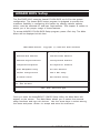
1
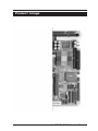
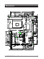
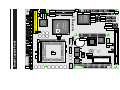
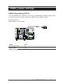
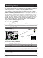
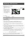
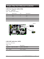
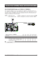
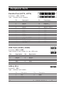
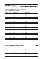
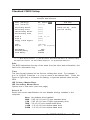
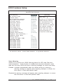
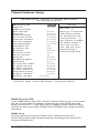
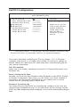
EmCORE-i6315 5¼" Pentium III Miniboard with 4x AGP SVGA or Flat Panel SVGA, Fast Ethernet, Audio, 16-bit Digital I/O, 4 Serial Ports and DiskOnChip socket Copyright © 2002 All Rights Reserved. Manual edition 1.2, April 2002 The information in this document is subject to change without prior notice in order to improve the reliability, design and function. It does not represent a commitment on the part of the manufacturer. Under no circumstances will the manufacturer be liable for any direct, indirect, special, incidental, or consequen-tial damages arising from the use or inability to use the product or documentation, even if advised of the possibility of such damages. This document contains proprietary information protected by copyright. All rights are reserved. No part of this manual may be reproduced by any mechanical, electronic, or other means in any form without prior written permission of the manufacturer. Trademarks ProSavage is a registered trademark of VIA Technologies. DiskOnChip ®2000 and TrueFFS are registered trademarks of M-Systems Inc.. PC is a registered trademark of International Business Machines Corporation. Intel is a registered trademark of Intel Corporation. AWARD is a registered trademark of Award Software International, Inc. Other product names mentioned herein are used for identification purposes only and may be trademarks and/or registered trademarks of their respective companies. Part number : 4011631500120 Table of Contents Specifications ................................................................................ 1 Ordering Codes ................................................................................................... 3 Product Image ............................................................................... 4 Dimensions ................................................................................... 5 Board Layout Front ....................................................................... 6 Jumper/Connector Quick Reference ............................................ 7 CMOS Jumper Settings ................................................................ 8 CMOS Operation(JRTC1) .................................................................................... 8 Watchdog Timer ............................................................................ 9 Mode Setting (JWDT1) ......................................................................................... 9 Time-out Setting (SWDT1) ................................................................................... 9 Programming Example ....................................................................................... 10 DiskOnChip® 2000 Flash Disk .................................................... 11 Installation Instructions ....................................................................................... 11 Single Chip Fast Ethernet Controller ......................................... 12 LAN Port Signals (LAN-CON) ............................................................................ 12 LAN LED Indicator (LED) ................................................................................... 12 Serial Port (COM2) Mode (RS232C/422/485) ............................... 13 RS-232/422/485 Mode on COM2 (JCOMSEL) ................................................... 13 Power Connectors ....................................................................... 14 Power Connectors (PWR) ................................................................................ 14 ATX power control (JP2) .................................................................................. 14 Chassis Auxilary Fan Connector (FAN1) .......................................................... 15 CPU Fan Connector (FAN3) .............................................................................. 15 Switches and Indicators ............................................................. 16 Interface Connectors HDD, FDD .................................................. 17 Floppy Disk Drive (FDD1) .................................................................................. 17 Enhanced IDE Connector (IDE1) ....................................................................... 18 Enhanced IDE Connector (IDE2) ....................................................................... 19 Peripheral Ports .......................................................................... 20 Parallel Port (LPT1, LPT2) .................................................................................. 20 USB Ports (USB1, USB2) .................................................................................. 21 IrDA (JIR1) .......................................................................................................... 21 Onboard RS-232 Serial Port (JCOM) ............................................................................................ 21 RS-422/485 Serial Ports (JRS1) ........................................................................ 21 Flat Panel VGA (LCD) ........................................................................................ 23 CRT SVGA (JVGA) ........................................................................................... 23 Keyboard (JKB&MS) ......................................................................................... 23 Audio Interface Port (JAUDIO) .......................................................................... 23 CDROM audio interface (SONY) ....................................................................... 23 16-bit General Purpose I/O (JDIO) ..................................................................... 24 System Resources ...................................................................... 25 C&T 69000 Flat Panel Controller ................................................ 28 LCD Voltage and Voltage Delay Selection (JVOLT1/JVOLT2) .......................... 28 Flat Panel Connector Power Setting ................................................................. 29 PLANAR EL640.480-AA1 ................................................................................. 30 KYOCERA KCB104VG2BA-A01 ....................................................................... 31 SHARP LQ12S41 ............................................................................................... 32 HITACHI LMG9211XUCC .................................................................................... 33 NAN YA LTBSHT024GC ..................................................................................... 34 TORISAN MXS121022010 ................................................................................. 35 NEC NL8060AC26-04 ........................................................................................ 36 AWARD BIOS Setup .................................................................... 38 Setup Items ........................................................................................................ 39 Standard CMOS Setup ....................................................................................... 40 IDE Harddisk Setup (submenu) ......................................................................... 42 BIOS Features Setup ......................................................................................... 44 Chipset Features Setup ..................................................................................... 46 Integrated Peripherals ....................................................................................... 53 Power Management Setup ................................................................................ 55 PnP/PCI Configuration ........................................................................................ 56 POST Codes ................................................................................ 59 Howto : Flash the BIOS ............................................................... 64 What if things go wrong .................................................................................... 65 Warranty ....................................................................................... 66 Specifications General Specifications CPU : Socket 370 FC-PGA/PPGA supports Intel ® Pentium®III, Intel® Celeron, VIA Cyrix®III with FSB @ 133 / 100 / 66 MHz Chipset : VIA ProSavage PM133 includes VT8605 Northbridge and VT82C686B Super Southbridge, supports PC-133, 133MHz FSB and ATA100 BIOS : AWARD Flash BIOS Green&Soft Off function, LS120, Multiple boot function Green Function : power saving supported in BIOS. DOZE /STANDBY / SUSPEND modes, ACPI & APM Secondary Cache : Integrated on CPU DRAM Memory : up to 512 MB of SDRAM in one 168-pin DIMM sockets (supports PC-133 SDRAM) Bus Interface : PCI-bus and PC/104-Plus (PCI+ISA) PCI Enhanced IDE with Ultra DMA : supports 2 ports and up to 4 ATAPI devices. Ultra DMA transfer 33/66 and 100 MB/sec one 40-pin (2.54 pitch) box header and one 44-pin (2.0 pitch) box header for 2.5" (laptop-size) HDD/Flash IDE drive including power lines. Watchdog Timer : generates an NMI or system RESET when your application loses control over the system. The timer interval is: 1, 2, 10, 20, 110 and 220 seconds . Real-time Clock : built-in chipset with lithium battery backup for 10 years of data retention. Network Interface Controller Chipset : Intel 82559, 10/100 Mbps, autoswitching Connector : 10-pin onboard header PC/104-Plus Interface Bus types : 104-pin ISA and 120-pin PCI Digital I/O Type : 16-bit GPIO, 8 independent GPI and 8 independent GPO programamble by software. High Speed Multi I/O Chipset : included in VT82C686B Super Southbridge Serial Ports : 3 high speed RS-232C ports (COM1,3,4) and one high speed RS-232/422/485 port (COM2) EmCORE-i6315 User's Manual 1 USB Ports : 4 ver 1.0 ports ( two 2x5-pin headers ) SIR Interface : onboard IrDA TX/RX port (5-pin header) Floppy Disk Drive Interface : 2 floppy disk drives, 5¼" (360 KB or 1.2 MB) and 3½" (720 KB, 1.44 MB or 2.88 MB). Bi-directional Parallel Port : SPP, EPP and ECP mode. Keyboard and Mouse Connectors : one combined 10-pin header for KB/Mouse Flash Disk DiskOnChip®2000 Package : Single Chip Flash Disk in 32-pin DIP JEDEC Capacity : up to 288 MByte Audio Chipset : 16-bit 3D AC'97 Audio controller integrated in VIA686B. Soundblaster Pro and Direct Sound compatible. LINE-in/out CD-in, Mic-in and stereo speakers. Connector : 10-pin onboard header Display Controller OPTION 1 Chipset : 4x AGP S3® Savage4 3D and S3® Savage 2000 2D engines integrated in VT8605 supports up to 32 MB (shared) memory Display Type : CRT (VGA, SVGA, XGA, SXGA) OPTION 2 Chipset : CHIPS C&T69030 HiQVideo Accelerator with 4 MB SDRAM on die Display Type : CRT, TFT, DSTN, SSTN, EL, Plasma Quarter VGA, VGA, SVGA, XGA and SXGA Environmental and Power Power Requirements : +5 V @ 4.8 A (typical), ±12 V ; (Pentium-III at 866 MHz and 128 MB PC-133 SDRAM) CPU Power : autodetect PWM switching power supply System Monitoring and Alarm : CPU and System temperature, system voltage and cooling fan RPM. Board Dimensions : 203 mm x 146 mm (5.75" x 8.0") Board Weight : 0.30 Kg. Operating Temperature : 0 to 60°C (32 to 140°F) 2 EmCORE-i6315 User's Manual Warning Single Board Computers and Miniboards contain very delicate Integrated Circuits (IC). To protect these components against damage from static electricity, always follow the following precautions when handling them : 1. Disconnect your board from the power source when you want to work on the inside 2. Hold the board by the edges and try not to touch the IC chips, leads or circuitry 3. Use a grounded wrist strap when handling computer components. 4. Place the board on a grounded antistatic pad or on the bag that came with the it, whenever it is separated from the system. Ordering Codes EmCORE-i6315/VL : 5.25" Socket 370 Pentium III / Celeron Littleboard Computer with AGP CRT SVGA, Fast Ethernet, AC97 Audio, 16-bit Digital I/O, 4 Serial Ports and DiskOnChip socket EmCORE-i6315/CL : same as above with Flat Panel / CRT Display support EmCORE-i6315 User's Manual 3 Product Image 4 EmCORE-i6315 User's Manual Dimensions 136.0 5.0 23.4 114.9 58.6 30.0 43.0 5.1 5.8 20.0 10.0 5.0 31.7 25.7 65.9 17.0 24.6 115.0 8.7 60.5 18.0 40.5 56.5 55.3 26.3 5.7 7.3 17.0 9.0 5.0 8.4 17.0 7.5 16.3 11.0 27.0 5.0 8.3 1.7 27.0 12.1 30.4 18.4 6.5 18.0 10.0 3.3 2.0 73.7 21.0 74.0 6.0 1.2 4.3 38.0 24.8 18.0 8.8 14.0 24.2 15.5 3.0 32.4 8.2 2.0 15.2 5.0 11.3 6.3 EmCORE-i6315 User's Manual 31.2 49.4 85.0 69.9 50.0 15.0 3.733.01.7 57.3 57.7 Ø 12.0 40.0 15.0 3.0 4.5 51.2 81.6 80.0 18.0 5.0 5.0 78.5 51.0 38.0 85.7 17.8 5.3 38.0 5.2 6.0 56.4 8.0 54.4 5 IDE1 JIR1 USB2 "Southbridge" VT82C686B REV : 1.0 EmCORE-i3615 VT8605 6 FDD "Northbridge" LCD C&T 69000 JP2 FAN3 JVOLT1 JVOLT2 JVGA JCOM JRS1 JKB&MS JCOMSEL USB1 SONY JDIO LPT1 LPT2 JAUDIO LAN-CON LAN-LED FAN1 Intel 82559 JWDT1 JFRNT PGA 370 RT2 JDOC1 SWDT1 ON 1 2 3 4 DiskOnChip2000 PWR 6 Board Layout Front i JRTC1 EmCORE-i6315 User's Manual RT1 IDE2 Jumper/Connector Quick Reference Jumpers Connectors JRTC1 CMOS Operation 2-3 -> Normal Operation 1-2 -> Clear CMOS JWDT1 Watchdog Active Mode 1-2 -> IOCHK 2-3 -> RESET off -> Disabled SWDT1 Watchdog Timer 1 2 3 4 off off on o f f off off on on off on off off off on o f f on on off off off on off o f f on Timeout Time 1 sec 2 sec 10 sec 20 sec 110 sec 220 sec JDOC1 DiskOnChip Base Address 1-2 -> D0000h 3-4 -> D8000h JVOLT1 /LCD voltage JVOLT1 Voltage 1-2 5 V 2-3 3.3 V JVOLT2 /LCD voltage delay JVOLT1 mode 1-2 immidiate 2-3 delayed EmCORE-i6315 User's Manual FAN1 CPU Fan Power FAN3 Auxilary Fan Power RT1 Temperature Sensor RT2 CPU Temperature Sensor LCD Flat Panel Connector JIR1 IrDA Header JKB&MS internal AT Keyboard JCOM COM 1/2/3/4 (RS-232) JDIO 16-bit DIO JRS1 COM 2 (RS-422/485) LPT1 Primary Parallel PORT LPT2 Secondary Parallel PORT USB1 1st/2nd USB port USB2 3rd/4th USB port JAUDIO Audio Connector SONY FDD 4-pin CDROM audio FDD interface IDE1 Primary IDE (40-pin) IDE2 Secondary IDE (44-pin) JVGA CRT SVGA PWR JP2 JFRNT 6-pin Power Connector ATX Power Control Signals, RESET, LEDs J1 Riser card cable Connector (For PCI riser card) 7 CMOS Jumper Settings CMOS Operation(JRTC1) If the EmCORE-i6315 refuses to boot due to inappropriate CMOS settings here is how to proceed to clear (reset) the CMOS to its default values Connector:JRTC1 Type:onboard 3-pin header 1 2 3 VT8605 "Northbridge" 6 "Southbridge" VT82C686B REV : 1.0 EmCORE-i3615 C&T 69000 JRTC1 i Intel 82559 PGA 370 ON 1 2 3 4 DiskOnChip2000 Mode Normal Operation JRTC1 2-3 Clear CMOS default setting 1-2 8 EmCORE-i6315 User's Manual Watchdog Timer The onboard watchdog timer can be disabled by jumper setting or enabled for either reboot by RESET or invoking an NMI.(non-maskable interrupt). Even if enabled by jumper setting upon boot the watchdog timer is always inactive. To initialize the watchdog timer reading of port 444H is sufficient. To disable the watchdog timer read port 44H. After the watchdog timer has been initialized by reading port 444H, it has to be strobed at preconfigured intervals to keep it from issuing a RESET or NMI. Intervals can also be selected by jumper setting. Strobing of the watchdog is done by reading port the same port that initializes the watchdog timer: port 444H. Failure to strobe before the configured period expires, indicating a program halt/abort, resulting in a RESET or NMI. Mode Setting (JWDT1) Watchdog Mode RESET JWDT1 2-3 I0CHK (Active NMI) 1-2 Disable Watchdog timer OFF default setting JWDT1 3 2 VT8605 "Northbridge" 6 REV : 1.0 "Southbridge" VT82C686B EmCORE-i3615 C&T 69000 1 i SW DT1 Intel 82559 PGA 370 ON ON 1 2 3 4 DiskOnChip2000 1 2 3 4 Time-out Setting (SWDT1) Watchdog Time-out Period 1 sec 1 OFF 2 OFF 3 ON 4 OFF 2 sec OFF OFF ON ON 10 sec OFF ON OFF OFF 20 sec OFF ON OFF ON 110 sec ON OFF OFF OFF 220 sec ON OFF OFF ON default setting EmCORE-i6315 User's Manual 9 Watchdog Timer Program Control Function Requirred Action Enable/refresh the Watch -Dog I/O Read 444H Disable the Watch-Dog Timer. I/O Read 044H Programming Example The following program is an examples of how to enable, disable and refresh the Watchdog timer: WDT_EN_RF EQU 444H WDT_DIS EQU 044H WT_Enable PUSH AX PUSH DX ;save AX MOV DX,WDT_EN_RF ;enable IN AL,DX POP DX POP AX DX the ;reco AX DX ;save AX DX watchdog RET WT_Rresh PUSH AX PUSH DX MOV DX,WDT_ET_RF ;refresh IN AL,DX POP DX POP AX ;reco the AX, watchdog DX RET WT_DISABLE PUSH AX PUSH DX MOV DX,WDT_DIS; IN AL,DX POP DX POP AX disable ;reco the AX, watchdog DX RET 10 EmCORE-i6315 User's Manual DiskOnChip® 2000 Flash Disk Installation Instructions 1. Make sure the EmCORE-i6315 is powered OFF. VT8605 "Northbridge" 6 "Southbridge" REV : 1.0 VT82C686B EmCORE-i3615 C&T 69000 JDOC1 2 1 i Intel 82559 PGA 370 2. Plug the DOC (DiskOnChip 2000) device into its socket. Verify the direction is correct (pin 1 of the DiskOnChip 2000 is aligned with pin 1 of the socket) 4 3 ON 1 2 3 4 DiskOnChip2000 3. Set address Base Address JDOC1 D0000h D8000h 1-2 3-4 default setting 4. Power up the system 5. During power up you may observe a message displayed by the DOC when its drivers are automatically loaded into systems memory 6. At this stage the DOC can be accessed as any disk in the system 7. If the DOC is the only disk in the system, it will appear as the first disk (drive C: in DOS) 8. If there are more disks besides the DOC, the DOC will appear by default as the last drive, unless it was programmed as first drive. (please refer to the DOC utilities user manual) 9. If you want the DOC to be bootable: a - copy the operating system files into the DOC by using the standard DOS command (for example: sys d:) b - The DOC should be the only disk in the systems or should be configured as the first disk in the system (c: ) using the DUPDATE utility For more information on DiskOnChip2000, visit M-Systems Web site at http:// www.m-sys.com where you can find Utilities Manual, Data Sheets and Application Notes. In addition, you can find the latest DiskOnChip 2000 S/W Utilities EmCORE-i6315 User's Manual 11 Single Chip Fast Ethernet Controller LAN Port Signals (LAN-CON) Connector : LAN-CON Type : Onboard 10-pin header Pin Description Pin Description 1 TX+ 2 TX- 3 RX+ 4 N/C 5 N/C 6 RX- 7 N/C 8 N/C 9 GND 10 GND LAN-CON VT8605 "Northbridge" 6 "Southbridge" VT82C686B REV : 1.0 EmCORE-i3615 C&T 69000 2 4 6 8 10 1 3 5 7 9 i Intel 82559 LAN-LED PGA 370 ON 1 2 3 4 DiskOnChip2000 10/ S A 100 P C D T LAN LED Indicator (LED) Connector: LED block Type: 3 LED LED Description (10)or100 / (light off) green 10MB/100MB Mode SPD / green Speed ACT / yellow Active Transfer 12 EmCORE-i6315 User's Manual Serial Port (COM2) Mode (RS232C/422/485) RS-232/422/485 Mode on COM2 (JCOMSEL) The onboard COM2 port can be configured to operate in RS-485 mode or in four different RS-422 modes. RS-422 modes differ in the way RX/TX is being handled. Jumper JCOMSEL determines between RS-232 or RS-422/485 and assigns the different RS-422 modes. NOTE : in RS-232 mode in RS-422/485 mode 2 4 COM2 is assigned to onboard connector JCOM COM2 is assigned to onboard connector JRS1 1 3 VT8605 "Northbridge" 6 REV : 1.0 2 4 6 8 10 12 1 3 5 7 JCOM SEL "Southbridge" VT82C686B EmCORE-i3615 C&T 69000 JRS1 9 11 i Intel 82559 PGA 370 ON 1 2 3 4 DiskOnChip2000 Mode Selection (JCOMSEL) RS-232C 1-2 off RS-485 on on on on off on RS-422 TX/RX always enabl RX enabl by RTS, TX always enabl TX enabl by RTS, RX always enabl TX/RX enabl by RTS default setting off off on on off on off on off off off off off off off off off off off off on on on on EmCORE-i6315 User's Manual 3-4 off 5-6 off 7-8 off 9-10 11-12 on off 13 Power Connectors Power Connectors (PWR) Connector : PWR Type : 4-pin onboard AT Connetor Pin Description wire color 1 +12V yellow 2 GND black 3 GND black 4 +5V red 1 6 VT8605 "Southbridge" REV : 1.0 VT82C686B C&T 69000 PWR "Northbridge" 3 2 1 EmCORE-i3615 JP2 Intel 82559 4 PGA 370 3 i 2 ON 1 2 3 4 DiskOnChip2000 ATX power control (JP2) Connector : JP2 Type : 3-pin onboard Wafer connector 14 Pin Description 1 5V SB(Standby) 2 GND 3 PS-ON EmCORE-i6315 User's Manual Chassis Auxilary Fan Connector (FAN1) Connector : FAN1 Type : 3-pin onboard header box Pin Description 1 GND 2 +12V 3 FAN_CTL VT8605 "Northbridge" 6 REV : 1.0 "Southbridge" VT82C686B EmCORE-i3615 3 2 1 C&T 69000 FAN1 i Intel 82559 PGA 370 ON 1 2 3 4 DiskOnChip2000 FAN3 1 2 3 CPU Fan Connector (FAN3) Connector : CHASFAN Type : 3-pin onboard header box Pin Description 1 GND 2 +12V 3 FAN_CTL EmCORE-i6315 User's Manual 15 VT8605 "Northbridge" 6 "Southbridge" REV : 1.0 VT82C686B EmCORE-i3615 C&T 69000 Switches and Indicators i Intel 82559 PGA 370 ON 1 2 3 4 DiskOnChip2000 JFRNT Green AC PI(+) LED GND Reset IDE LED GND Reset Vcc(+) Active Pow er PW RBT Sw itch GND SM I Sw itch GND SM I (+)Vcc NC GND Pow er LED KB LOCK Keyboard Lock GND V cc NC NC S PKIN Speaker Note : (+) means LED anode 16 EmCORE-i6315 User's Manual Interface Connectors HDD, FDD 1 Floppy Disk Drive (FDD1) 2 Connector : FDD1 Type : Onboard 34-pinheader Pin Description Pin Description 1 GND 2 DRIVE DENSITY SELECT 0 3 GND 4 DRIVE DENSITY SELECT 1 5 GND 6 N/C 7 GND 8 INDEX- 9 GND 10 MOTOR ENABLE A- 11 GND 12 DRIVER SELECT B- 13 GND 14 DRIVER SELECT A- 15 GND 16 MOTOR ENABLE B- 17 GND 18 DIRECTION- 19 GND 20 STEP- 21 GND 22 WRITE DATA- 23 GND 24 WRITE GATE- 25 GND 26 TRACK 0- 27 GND 28 WRITE PROTECT- 29 GND 30 READ DATA- 31 GND 32 HEAD SELECT- 33 GND 34 DISK CHANGE- EmCORE-i6315 User's Manual 33 34 17 1 2 Enhanced IDE Connector (IDE1) Connector : IDE1 and IDE2 Type : onboard 40-pin box headers, primary IDE Pin Description 1 RESET 2 GND 3 D7 4 D8 5 D6 6 D9 7 D5 8 D10 9 D4 10 D11 11 D3 12 D12 13 D2 14 D13 15 D1 16 D14 17 D0 18 D15 19 GND 20 N/C 21 REQ 22 GND 23 IOW-/STOP 24 GND 25 IOR-/HDMARDY 26 GND 27 IORDY/DDMARDY 28 IDESEL 29 DACK- 30 GND 31 IRQ 32 N/C 33 A1 34 CBLID 35 A0 36 A2 37 CS0(MASTER CS) 38 CS1(SLAVE CS) 39 LED ACT- 40 GND 18 Pin Description EmCORE-i6315 User's Manual Enhanced IDE Connector (IDE2) 44-pin (2.0 pitch) box header for 2.5" (laptop-size) HDD/Flash IDE drive includinging power signals Connector : IDE2 Type : onboard 44-pin box header, secondary IDE Pin Description Pin Description 1 RESET 2 GND 3 D7 4 D8 5 D6 6 D9 7 D5 8 D10 9 D4 10 D11 11 D3 12 D12 13 D2 14 D13 15 D1 16 D14 17 D0 18 D15 19 GND 20 N/C 21 REQ 22 GND 23 IOW-/STOP 24 GND 25 IOR-/HDMARDY 26 GND 27 IORDY/DDMARDY 28 IDESEL 29 DACK- 30 GND 31 IRQ 32 N/C 33 A1 34 CBLID 35 A0 36 A2 37 CS0(MASTER CS) 38 CS1(SLAVE CS) 39 LED ACT- 40 GND 41 Vcc 42 Vcc 43 GND 44 GND EmCORE-i6315 User's Manual 19 Peripheral Ports Parallel Port (LPT1, LPT2) 13 26 1 14 Connector : LPT1 / LPT2 Type : Onboard 26-pin headers 13 26 1 14 Pin Description Pin Description 1 STROBE- 14 AUTO FEED- 2 DATA0 15 ERROR- 3 DATA1 16 INITIALIZE- 4 DATA2 17 SELECT INPUT- 5 DATA3 18 GND 6 DATA4 19 GND 7 DATA5 20 GND 8 DATA6 21 GND 9 DATA7 22 GND 10 ACKNOWLEDGE- 23 GND 11 BUSY 24 GND 12 PAPER EMPTY 25 GND 13 SELECT+ 26 N/C 2 4 6 8 10 USB Ports (USB1, USB2) 1 3 5 7 9 Connector: USB1 / USB2 Type:onboard 10-pin header for two USB ports Pin Description Pin Description 1 VCC 2 VCC 3 DATA0- 4 DATA1- 5 DATA0+ 6 DATA1+ 7 GND 8 GND 9 GND 10 GND 2 4 6 8 10 1 3 5 7 9 IrDA (JIR1) 1 2 3 4 5 Connector : JIR1 Type : onboard 5-pin header 20 Pin Description Pin Description 1 2 4 Vcc NC GND 3 5 IRRX IRTX EmCORE-i6315 User's Manual Onboard RS-232 Serial Port (JCOM) 2 1 40 39 Connector : JCOM (COM1, COM2, COM3, COM4) Type : 4x onboard 10-pin headers COM1 Pin Description Pin Description 1 DCD 2 RXD 3 TXD 4 DTR 5 GND 6 DSR 7 RTS 8 CTS 9 RI 10 N/C 11 DCD 12 RXD 13 TXD 14 DTR 15 GND 16 DSR 17 RTS 18 CTS 19 RI 20 N/C 21 DCD 22 RXD 23 TXD 24 DTR 25 GND 26 DSR 27 RTS 28 CTS 29 RI 30 N/C 31 DCD 32 RXD 33 TXD 34 DTR 35 GND 36 DSR 37 RTS 38 CTS 39 RI 40 N/C COM2 COM3 COM4 2 4 RS-422/485 Serial Ports (JRS1) 1 3 Connector : JRS1 Type : onboard 4-pin header (COM2) COM2 Pin Description Pin 1 TX- / 485- 3 TX+ / 485+ 2 RX+ 4 RX- EmCORE-i6315 User's Manual Description 21 Flat Panel VGA (LCD) 2 1 Connector : LCD Type : Onboard 50-pin box header Pin 1 3 5 7 9 11 13 15 17 19 21 23 25 27 29 31 33 35 37 39 41 43 45 47 49 Description +12V GND VCC_LCD ENAVEE P0 P2 P4 P6 P8 P10 P12 P14 P16 P18 P20 P22 P24 SHFCLK M GND P26 P28 P30 P32 P34 Pin 2 4 6 8 10 12 14 16 18 20 22 24 26 28 30 32 34 36 38 40 42 44 46 48 50 Description +12V GND ENAVDD GND P1 P3 P5 P7 P9 P11 P13 P15 P17 P19 P21 P23 P25 FLM LP ENABKL P27 P29 P31 P33 P35 1 2 CRT SVGA (JVGA) Connector : JVGA Type : onboard 16-pin header 22 Pin Description Pin Description 1 RED 2 GREEN 3 BLUE 4 N/C 5 GROUND 6 GROUND 7 GROUND 8 GROUND 9 N/C 10 GROUND 11 N/C 12 VDDAT 13 HSYNC 14 VSYNC 15 VDCCLK 16 N/C EmCORE-i6315 User's Manual Keyboard (JKB&MS) 2 4 6 8 10 Connector : JKB&MS Type : Onboard 10-pin header 1 3 5 7 9 Pin Description Pin Description 1 3 5 7 9 KB-DATA N/C GND Vcc KB-CLK 2 4 6 8 10 MS-DATA NC GND Vcc MS-CLK Audio Interface Port (JAUDIO) 2 4 6 8 10 Connector : JAUDIO Type : onboard 10-pin header 1 3 5 7 9 Pin Description Pin Description 1 LINE RIGHT 2 GND 3 LINE LEFT 4 MIC 5 MIC 6 GND 7 N/C 8 SPEAKER LEFT 9 SPEAKER RIGHT 10 GND 3 4 CDROM audio interface (SONY) 1 2 Connector : SONY Type : onboard 4-pin boxheader Pin Description Pin Description 1 CD Left 2 GND 3 GND 4 CD Right EmCORE-i6315 User's Manual 23 16-bit General Purpose I/O (JDIO) 1 2 Connector : JDIO Type : Onboard 20-pin header Pin 1 3 5 7 9 11 13 15 17 19 24 Description DO0 DO2 DO4 DO6 GND DI0 DI2 DI4 DI6 +5V Pin 2 4 6 8 10 12 14 16 18 20 20 19 Description DO1 DO3 DO5 DO7 GND DI1 DI3 DI5 DI7 +12V EmCORE-i6315 User's Manual System Resources Interrupt Assignment IRQ Address Description 0 System Timer 1 Keyboard (KB output buffer full) 2 Programmable Interrupt Controller 3 Serial Port 2 4 Serial Port 1 5 Parallel Port 2 6 Floppy controller 7 Parallel Port 1 8 Real-Time Clock 9 Software Redirected IRQ2 10 Reserved 11 Reserved 12 Reserved 13 Coprocessor 14 Primary IDE Controller 15 Secondary IDE Controller Memory Mapping Adress Size Description 00000000h-0009FFFFh 640K Host access map to the main memory 000A0000h-000BFFFFh 128K Reserved for Video frame buffer 000C0000h-000C3FFFh 16K Reserved for VGA BIOS 000C4000h-000C7FFFh 16K Reserved for VGA BIOS 000C8000h-000CBFFFh 16K Reserved for ROM device 000CC000h-000CFFFFh 16K Reserved for ROM device 000D0000h-000DFFFFh 64K Reserved for ROM device EmCORE-i6315 User's Manual 25 I/O Adress Mapping IO address Description Notes 0000h-000Fh DMA controller 1 registers 0010h-001Ch Local Bus configuration registers 0020h-0021h Interrupt controller 1 registers. 0040h-0043h Timer/Counter registers 0060h-0064h Keyboard shadow registers 0070h-0071h NMI Mask control registers 0080h-008Fh DMA Page registers. 0094h Mother-board VGA enable 00A0h-00A1h Interrupt controller 2 registers 00B1h ISA standard Port B 00C0h-00DFh DMA controller 2 registers 0102h VGA setup register. 03B4h,03B5h,03BAh 03D4h,03D5h,03DAh 03C0h-03CFh VGA registers. 0CF8h PCI configuration Address register. 0CFCh-0CFFh PCI configuration Data register. 46E8h VGA add-in mode enable register. 26 EmCORE-i6315 User's Manual This page intetionally left blank EmCORE-i6315 User's Manual 27 C&T 69000 Flat Panel Controller EmCORE-i6315CL only ! The 69000 is the first member of CHIPS's HiQVideo family to integrate high speed SDRAM frame buffer memory into the chip. Using leading edge embedded memory logic technologies, the 69000 integrates 2 MBytes of SDRAM into the chip. By embedding SDRAM and graphics controller logic on the same die, the 69000 delivers uncompromised performance and at the same time consumes much less power than the discrete solution. The integrated SDRAM supports up to 83MHz operation, which provides up to 664MBytes/second frame buffer bandwidth. The increase in the frame buffer bandwidth enables the 69000 to support high color, high-resolution graphics modes and real-time video acceleration. Supported Display Modes : Resolution Colors 1280x1024 8bpp 60 Hz 1024x768 16bpp 60,75,85 Hz 800x600 24bpp 60,75,85 Hz 640x480 24bpp 60,75,85 Hz 28 Refresh Rate EmCORE-i6315 User's Manual Flat Panel Connector Power Setting The EmCORE-i6315 's Vcc is configurable as either +3.3 or +5.0 Volt by jumper setting (JVOLT1) A second jumper (JVOLT2) delays applying power to the LCD's backlight when booting your system. Enabling this delay only initializes the backlight after the LCD itself is initialized. The function is mainly cosmetic. +12 V GND V CC FPVEE P0 P2 P4 P6 P8 P10 P12 P14 P16 P18 P20 P22 P24 SHFCLK M GND P26 P28 P30 P32 P34 1 3 5 7 9 11 13 15 17 19 21 23 25 27 29 31 33 35 37 39 41 43 45 47 49 2 4 6 8 10 12 14 16 18 20 22 24 26 28 30 32 34 36 38 40 42 44 46 48 50 +12 V GND ENA V DD GND P1 P3 P5 P7 P9 P11 P13 P15 P17 P19 P21 P23 P25 FLM LP ENABKL P27 P29 P31 P33 P35 VT8605 "Northbridge" 6 REV : 1.0 JVOLT1 JVOLT2 1 2 3 "Southbridge" VT82C686B EmCORE-i3615 C&T 69000 LCD Voltage and Voltage Delay Selection (JVOLT1/JVOLT2) i Intel 82559 PGA 370 ON 1 2 3 4 Connectors : JVOLT1 / JVOLT2 Type : onboard 3-pin header Vcc JVOLT1 +3.3 +5.0 2-3 1-2 DiskOnChip2000 default setting Delay Mode JVOLT12 delayed no delay 2-3 1-2 default setting EmCORE-i6315 User's Manual 29 PLANAR EL640.480-AA1 Display type : 640 x 480 EL Mono 30 EL 640.480-AA1/ 34-pin 2.54 pitch / housing EMCORE-I6315 / 50-pin 2.0 pitch / housing Pin 1 2 3 4 5 6 7 8 9 10 11 12 13 14 15 16 17 18 19 20 21 22 23 24 25 26 27 28 29 30 31 32 33 34 J2(1) J2(2) J2(3) J2(4) J3(1) J3(2) Pin 39 21 39 22 39 23 Description GND PD12 GND PD13 GND PD14 24 PD15 39 GND 3 35 3 40 3 38 GND SHFCLK GND ENABKL GND LP 36 FLM 6 PVCC 1 4 4 5 5 4 +12V GND GND VCC VCC GND Description GND D0 GND D1 GND D2 N/C D3 N/C Reserved N/C Reserved N/C Reserved GND Reserved GND VCLK GND _BLANK GND HS N/C VS N/C N/C N/C ENABLE VMODE N/C N/C N/C Reserved Reserved +12Vdc GND GND +5Vdc LUM GND EmCORE-i6315 User's Manual KYOCERA KCB104VG2BA-A01 Display type : 640 x 480 16-bit Color STN KCB104VG2BA-A01 Molex 53261-1510 EMCORE-I6315 / 50-pin 2.0 pitch / housing Pin 1 2 3 4 5 6 7 8 9 10 11 12 13 14 15 Pin 36 --40 38 39 35 39 20 19 18 17 12 11 10 9 Description FLM NC DISP LOAD VSS CP VSS HD0 HD1 HD2 HD3 HD4 HD5 HD6 HD7 Description FLM --ENABKL LP GND SHFCLK GND P11 P10 P9 P8 P3 P2 P1 P0 KCB104VG2BA-A01 Molex 53261-1410 EMCORE-I6315 / 50-pin 2.0 pitch / housing Pin 1 2 3 4 5 6 7 8 9 10 11 12 13 14 Pin 24 23 22 21 16 15 14 13 5 3 --------- Description LD0 LD1 LD2 LD3 LD4 LD5 LD6 LD7 VDD VSS NC NC NC VCONT EmCORE-i6315 User's Manual Description P15 P14 P13 P12 P7 P6 P5 P4 +5V GND ------+0.8~+2.8V 31 SHARP LQ12S41 Display type : 800 x 600 18-bit Color TFT 32 LQ12S41 DF9X-41S-1V/Hirose EMCORE-I6315 / 50-pin 2.0 pitch / housing Pin 1 2 3 4 5 6 7 8 9 10 11 12 13 14 15 16 17 18 19 20 21 22 23 24 25 26 27 28 29 30 31 32 33 34 35 36 37 38 39 40 41 Pin 39 35 39 38 36 39 39 39 27 28 29 4 30 31 32 4 4 4 19 20 21 8 22 23 24 8 8 8 11 12 13 3 14 15 16 3 37 --5 5 --- Description GND CLK GND Hsync Vsync GND GND GND R0 R1 R2 GND R3 R4 R5 GND GND GND G0 G1 G2 GND G3 G4 G5 GND GND GND B0 B1 B2 GND B3 B4 B5 GND DE R/L VCC VCC U/P Description GND SHFCLK GND LP FLM GND GND GND P18 P19 P20 GND P21 P22 P23 GND GND GND P10 P11 P12 GND P13 P14 P15 GND GND GND P2 P3 P4 GND P5 P6 P7 GND M --+3.3V +3.3V --- EmCORE-i6315 User's Manual HITACHI LMG9211XUCC Display type : 640 x 480 16-bit Color STN LMG9211XUCC Molex 53261-1510 EMCORE-I6315 / 50-pin 2.0 pitch / housing Pin 1 2 3 4 5 6 7 8 9 10 11 12 13 14 15 Pin 36 --40 38 39 35 39 20 19 18 17 12 11 10 9 Description FLM NC DISP·OFF LOAD VSS CP VSS UD0 UD1 UD2 UD3 UD4 UD5 UD6 UD7 Description FLM --ENABKL LP GND SHFCLK GND P11 P10 P9 P8 P3 P2 P1 P0 LMG9211XUCC Molex 53261-1410 EMCORE-I6315 / 50-pin 2.0 pitch / housing Pin 1 2 3 4 5 6 7 8 9 10 11 12 13 14 Pin 24 23 22 21 16 15 14 13 5 3 3 ------- Description LD0 LD1 LD2 LD3 LD4 LD5 LD6 LD7 VDD VSS VSS VEE VEE VO EmCORE-i6315 User's Manual Description P15 P14 P13 P12 P7 P6 P5 P4 +5V GND GND +27V +27V +27V 33 NAN YA LTBSHT024GC Display type : 640 x 480 8-bit Mono STN 34 LTBSHT024GC Molex 53261-1590 EMCORE-I6315 / 50-pin 2.0 pitch / housing Pin 1 2 3 4 5 6 7 8 9 10 11 12 13 14 15 Pin 36 38 35 40 5 39 -12 11 10 9 16 15 14 13 Description FLM LOAD CP D.OFF VDD VSS VEE DU0 DU1 DU2 DU3 DL0 DL1 DL2 DL3 Description FLM LP SHFCLK ENABKL VCC GND -17V P3 P2 P1 P0 P7 P6 P5 P4 EmCORE-i6315 User's Manual TORISAN MXS121022010 Display type : 800 x 600 18-bit Color TFT MXS121022010 DF9X-41S-1V/Hirose EMCORE-I6315 / 50-pin 2.0 pitch / housing Pin 1 2 3 4 5 6 7 8 9 10 11 12 13 14 15 16 17 18 19 20 21 22 23 24 25 26 27 28 29 30 31 32 33 34 35 36 37 38 39 40 41 Pin 3 35 3 38 36 3 3 3 27 28 29 4 30 31 32 4 4 4 19 20 21 8 22 23 24 8 8 8 11 12 13 39 14 15 16 39 37 39 5 5 --- Description GND DCLK GND Hsync Vsync GND GND GND R0 R1 R2 GND R3 R4 R5 GND GND GND G0 G1 G2 GND G3 G4 G5 GND GND GND B0 B1 B2 GND B3 B4 B5 GND DE TEST VCC VCC MODE EmCORE-i6315 User's Manual Description GND SHFCLK GND LP FLM GND GND GND P18 P19 P20 GND P21 P22 P23 GND GND GND P10 P11 P12 GND P13 P14 P15 GND GND GND P2 P3 P4 GND P5 P6 P7 GND M GND +3.3V +3.3V --- 35 NEC NL8060AC26-04 Display type : 800 x 600 18-bit Color TFT 36 NL8060AC26-04 DF9X-41S-1V/Hirose EMCORE-I6315 / 50-pin 2.0 pitch / housing Pin 1 2 3 4 5 6 7 8 9 10 11 12 13 14 15 16 17 18 19 20 21 22 23 24 25 26 27 28 29 30 31 32 33 34 35 36 37 38 39 40 41 Pin 39 35 39 38 36 39 39 39 27 28 29 4 30 31 32 4 4 4 19 20 21 8 22 23 24 8 8 8 11 12 13 3 14 15 16 3 37 5 5 5 --- Description GND CLK GND Hsync Vsync GND GND GND R0 R1 R2 GND R3 R4 R5 GND GND GND G0 G1 G2 GND G3 G4 G5 GND GND GND B0 B1 B2 GND B3 B4 B5 GND DE VCC VCC VCC MODE Description GND SHFCLK GND LP FLM GND GND GND P18 P19 P20 GND P21 P22 P23 GND GND GND P10 P11 P12 GND P13 P14 P15 GND GND GND P2 P3 P4 GND P5 P6 P7 GND M +3.3V/+5V +3.3V/+5V +3.3V/+5V --- EmCORE-i6315 User's Manual This page intetionally left blank EmCORE-i6315 User's Manual 37 AWARD BIOS Setup The EmCORE-i6315 uses the Award PCI/ISA BIOS ver 6.0 for the system configuration. The Award BIOS setup program is designed to provide the maximum flexibility in configuring the system by offering various options which could be selected for end-user requirements. This chapter is written to assist you in the proper usage of these features. To access AWARD PCI/ISA BIOS Setup program, press <Del> key. The Main Menu will be displayed at this time. CMOS SETUP UTILITY - Copyright (C) 1984-2001 Award Software Standard CMOS Features Frequency/Voltage Control Advanced BIOS Features Load Fail-Safe Defaults Advanced Chipset Features Load Optimized Defaults Integrated Peripherals Set Supervisor Password Power Management Setup Set User Password PnP/PCI Configurations Save & Exit Setup PC Health Status Exit Without Saving Esc: Quit F10: Save and Exit ¯®¬ : Select Item Time, Date, Hard Disk Type Once you enter the AwardBIOS CMOS Setup Utility, the Main Menu will appear on the screen. The Main Menu allows you to select from several setup functions and two exit choices. Use the arrow keys to select among the items and press <Enter> to accept and enter the sub-menu. 38 EmCORE-i6315 User's Manual Setup Items The main menu includes the following main setup categories. Recall that some systems may not include all entries. Standard CMOS Features Use this menu for basic system configuration. Advanced BIOS Features Use this menu to set the Advanced Features available on your system. Advanced Chipset Features Use this menu to change the values in the chipset registers and optimize your system's performance. Integrated Peripherals Use this menu to specify your settings for integrated peripherals. Power Management Setup Use this menu to specify your settings for power management. PnP / PCI Configuration This entry appears if your system supports PnP / PCI. Frequency/Voltage Control Use this menu to specify your settings for frequency/voltage control. Load Fail-Safe Defaults Use this menu to load the BIOS default values for the minimal/stable performance for your system to operate. Load Optimized Defaults Use this menu to load the BIOS default values that are factory settings for optimal performance system operations. While Award has designed the custom BIOS to maximize performance, the factory has the right to change these defaults to meet their needs. Supervisor / User Password Use this menu to set User and Supervisor Passwords. Save & Exit Setup Save CMOS value changes to CMOS and exit setup. Exit Without Saving Abandon all CMOS value changes and exit setup. EmCORE-i6315 User's Manual 39 Standard CMOS Setup CMOS SETUP UTILITY - Copyright (C) 1984-2001 Award Software Standard CMOS Features Date: (mm:dd:yy) Time: (hh:mm:ss) Fri, Feb 23 2001 16:19:20 IDE IDE IDE IDE [None] [None] [None] [None] Primary Master Primary Slave Secondary Master Secondary Slave Item Help 2001 Change the day, month, year and century Drive A Drive B Floppy 3 Mode Support 1.44M, 3.5 in. [None] [None] Video Halt On [EGA/VGA] [All , but Keyboard] Base Memory Extended Memory Total Memory 640K 252928K 253952K ¯ ® ¬ :Move Enter:Select +/-/PU/PD:Value F10:Save ESC:Exit F1:General Help F5:Previous Values F6:Fail-SAfe Defaults F7:Optimized Defaults Date The BIOS determines the day of the week from the other date information; this field is for information only. Time The time format is based on the 24-hour military-time clock. For example, 1 p.m. is 13:00:00. Press the « or ( key to move to the desired field . Press the PgUp or PgDn key to increment the setting, or type the desired value into the field. IDE Primary Master/Slave IDE Secondary Master/Slave Options are in sub menu (see next page) Drive A, B Select the correct specifications for the diskette drive(s) installed in the computer. None : No diskette drive installed 360K : 5.25 in5-1/4 inch PC-type standard drive 1.2M : 5.25 in5-1/4 inch AT-type high-density drive 720K : 3.5 in3-1/2 inch double-sided drive 1.44M : 3.5 in3-1/2 inch double-sided drive 2.88M : 3.5 in3-1/2 inch double-sided drive 40 EmCORE-i6315 User's Manual Floppy Mode 3 Support Enables support for 1.2 MB format capacity on 3½" disk drives. This format is commonly used Japan. Options are : disabled, drive A, drive B, both. Video Select the type of primary video subsystem in your computer. The BIOS usually detects the correct video type automatically. The BIOS supports a secondary video subsystem, but you do not select it in Setup. Halt On During the power-on self-test (POST), the computer stops if the BIOS detects a hardware error. You can tell the BIOS to ignore certain errors during POST and continue the boot-up process. These are the selections: No errors POST does not stop for any errors. All errors If the BIOS detects any non-fatal error, POST stops and prompts you to take corrective action. All, But Keyboard POST does not stop for a keyboard error, but stops for all other errors. All, But Diskette POST does not stop for diskette drive errors, but stops for all other errors. All, But Disk/Key POST does not stop for a keyboard or disk error, but stops for all other errors. EmCORE-i6315 User's Manual 41 IDE Harddisk Setup (submenu) CMOS SETUP UTILITY - Copyright (C) 1984-2001 Award Software IDE Primary Master IDE HDD Auto-Detection Press Enter Item Help 2001 IDE Primary Master Access Mode [Auto] [Auto] Menu Level Capacity 0 MB Cylinder Head Precomp Landing Zone Sector 0 0 0 0 0 ¯ ® ¬ :Move Enter:Select +/-/PU/PD:Value F10:Save ESC:Exit F1:General Help F5:Previous Values F6:Fail-SAfe Defaults F7:Optimized Defaults IDE HDD Auto-detection Press Enter to auto-detect the HDD on this channel. If detection is successful, it fills the remaining fields on this menu. IDE Primary Master Selecting 'manual' lets you set the remaining fields on this screen. Selects the type of fixed disk. "User Type" will let you select the number of cylinders, heads, etc. Note: PRECOMP=65535 means NONE ! Capacity Disk drive capacity (Approximated). Note that this size is usually slightly greater than the size of a formatted disk given by a disk checking program. Access Mode Normal, LBA, Large or Auto Choose the access mode for this hard disk The following options are selectable only if the 'IDE Primary Master' item is set to 'Manual' 42 EmCORE-i6315 User's Manual Cylinder Min = 0 Max = 65535 Set the number of cylinders for this hard disk. Head Min = 0 Max = 255 Set the number of read/write heads Precomp Min = 0 Max = 65535 **** Warning: Setting a value of 65535 means no hard disk Landing zone Min = 0 Max = 65535 **** Warning: Setting a value of 65535 means no hard disk Sector Min = 0 Max = 255 Number of sectors per track We recommend that you select Type "AUTO" for all drives. The BIOS will auto-detect the hard disk drive and CD-ROM drive at the POST stage. If your hard disk drive is a SCSI device, please select "None" for your hard drive setting. EmCORE-i6315 User's Manual 43 BIOS Features Setup CMOS SETUP UTILITY - Copyright (C) 1984-2001 Award Software Advanced BIOS Features Virus Warning CPU Internal Cache External Cache CPU L2 Cache ECC Checking Quick Power On Self Test First Boot device Second Boot device Third Boot device Boot other device Swap Floppy Drive Boot Up Floppy Seek Boot Up NumLock Status Gate A20 Option Typematic Rate Setting Typematic Rate (Chars/Sec) 6 Typematic Delay (Msec) Security Option OS Select For DRAM > 64MB Video BIOS Shadow C8000-CBFFF Shadow CC000-CFFFF Shadow D0000-D3FFF Shadow D4000-D7FFF Shadow D8000-DBFFF Shadow DC000-DFFFF Shadow [Enabled] [Enabled] [Enabled] [Enabled] [Disabled] [Floppy] [HDD-0] [Floppy] [Disabled] [Disabled] [Disabled] [Off] [Normal] [Disabled] Item Help Menu Level Allows you to choose the VIRUS warning feature for IDE Hard Disk boot sector protection. If this function is enabled and someone attempt to write data into this area, BIOS will show a warning message on screen and alarm beep 250 [Setup] [Non-OS2] [Enabled] [Disabled] [Disabled] [Disabled] [Disabled] [Disabled] [Disabled] ¯ ® ¬ :Move Enter:Select +/-/PU/PD:Value F10:Save ESC:Exit F1:General Help F5:Previous Values F6:Fail-SAfe Defaults F7:Optimized Defaults Virus Warning Allows you to choose the VIRUS Warning feature for IDE Hard Disk boot sector protection. If this function is enabled and someone attempt to write data into this area, BIOS will show a warning message on screen and beep. Enabled Activates automatically when the system boots up causing a warning message to appear when anything attempts to access the boot sector or hard disk partition table. Disabled No warning message will appear when anything attempts to access the boot sector or hard disk partition table. 44 EmCORE-i6315 User's Manual CPU Internal Cache/External Cache These two categories speed up memory access. However, it depends on CPU/chipset design. Enabled : Enable cache, Disabled : Disable cache CPU L2 Cache ECC Checking This item allows you to enable/disable CPU L2 Cache ECC checking. The choice: Enabled, Disabled. Quick Power On Self Test This category speeds up Power On Self Test (POST) after you power up the computer. If it is set to Enable, BIOS will shorten or skip some check items during POST. Enabled : Enable quick POST. Disabled : Normal POST First/Second/Third/Other Boot Device The BIOS attempts to load the operating system from the devices in the sequence selected in these items. The choices are : Floppy, LS/ZIP, HDD, SCSI, CDROM, Disabled. Swap Floppy Drive If the system has two floppy drives, you can swap the logical drive name assignments. The choice: Enabled/Disabled. Boot Up Floppy Seek Seeks disk drives during boot up. Disabling speeds boot up. The choice: Enabled/Disabled. Boot Up NumLock Status Select power on state for NumLock. The choice: Enabled/Disabled. Gate A20 Option Select if chipset or keyboard controller should control GateA20. Normal A pin in the keyboard controller controls GateA20 Fast Lets chipset control GateA20 Typematic Rate Setting Key strokes repeat at a rate determined by the keyboard controller. When enabled, the typematic rate and typematic delay can be selected. The choice: Enabled/Disabled. Typematic Rate (Chars/Sec) Sets the number of times a second to repeat a key stroke when you hold the key down. The choice: 6, 8, 10, 12, 15, 20, 24, 30. Typematic Delay (Msec) Sets the delay time after the key is held down before it begins to repeat the keystroke. The choice: 250, 500, 750, 1000. EmCORE-i6315 User's Manual 45 Security Option Select whether the password is required every time the system boots or only when you enter setup. System The system will not boot and access to Setup will be denied if the correct password is not entered at the prompt. Setup The system will boot, but access to Setup will be denied if the correct password is not entered at the prompt. Note To disable security, select PASSWORD SETTING at Main Menu and then you will be asked to enter password. Do not type anything and just press <Enter>, it will disable security. Once the security is disabled, the system will boot and you can enter Setup freely. OS Select For DRAM > 64MB Select the operating system that is running with greater than 64MB of RAM on the system.The choice: Non-OS2, OS2. Video BIOS Shadow Enabled this copies the video BIOS from ROM to RAM. effectively enhancing performance, and reducing the amount of upper memory available by 32KB (the C0000~C7FFF area of memory between 640 KB and 1 MB is used). C8000-CBFFF Shadow Enabling any of the C8000~CBFFF segments allows components to move their firmware into these upper memory segments. However your computer can lock-up doing so, because some devices don't like being shadowed at those particular 16 KB segments of upper memory. Note - In Windows 95, double click 'Computer' within Device Manager and select 'Memory'. This will tell you what segments (if any) are being shadowed For DOS you can use MSD.EXE to see what segments are claimed. CC000-CFFFF - D0000-D3FFF - D4000-D7FFF - D8000-DBFFF and DC000-DFFFF - Same as above. 46 EmCORE-i6315 User's Manual Chipset Features Setup CMOS SETUP UTILITY - Copyright (C) 1984-2001 Award Software Advanced Chipset Features DRAM Timing by SPD DRAM Clock SDRAM Cycle Length Bank Interleave Memory Hole P2C/C2P Concurrency Fast R-W Turn Around System BIOS Cacheable Video BIOS Cacheable Video RAM Cacheable Frame Buffer Size AGP Aperture Size AGP-4X Mode AGP Driving Control AGP Driving Value Onchip USB USB Keyboard Support OnChip Sound CPU to PCI Write Buffer PCI Dynamic Bursting PCI Master 0 WS Write PCI Delay Transaction PCI#2 Access #1 Retry AGP Master 1 WS Write AGP Master 1 WS Read [Enabled] Host CLK 3 Disabled [Disabled] [Enabled] [Disabled] [Disabled] [Disabled] [Disabled] [8M] [64M] [Enabled] [Auto] DA [Enabled] [Disabled] [Auto] [Enabled] [Enabled] [Enabled] [Disabled] [Enabled] [Enabled] [Disabled] Item Help Menu Level Allows you to choose the VIRUS warning feature for IDE Hard Disk boot sector protection. If this function is enabled and someone attempt to write data into this area, BIOS will show a warning message on screen and alarm beep ¯ ® ¬ :Move Enter:Select +/-/PU/PD:Value F10:Save ESC:Exit F1:General Help F5:Previous Values F6:Fail-SAfe Defaults F7:Optimized Defaults DRAM Timing By SPD If your DIMM memory have SPD ( Serial Presence Detect ) 8-pin IC on module, you can set this option to Enabled. System will set your DRAM clock and timing from the SPD IC. If the option set as Disabled, DRAM clock and timing must be set from items below. (DRAM Clock, SDRAM Cycle Length and Bank Interleave) DRAM Clock This item allows you to set the DRAM Clock. Options are Host CLK, HCLK+33M or HCLK-33M. Please set the item according to the Host (CPU) Clock and DRAM Clock. EmCORE-i6315 User's Manual 47 SDRAM Cycle Length This feature is similar to SDRAM CAS Latency Time. It controls the time delay (in clock cycles - CLKs) that passes before the SDRAM starts to carry out a read command after receiving it. This also determines the number of CLKs for the completion of the first part of a burst transfer. Thus, the lower the cycle length, the faster the transaction. However, some SDRAM cannot handle the lower cycle length and may become unstable. So, set the SDRAM Cycle Length to 2 for optimal performance if possible but increase it to 3 if your system becomes unstable. Bank Interleave This feature enables you to set the interleave mode of the SDRAM interface. Interleaving allows banks of SDRAM to alternate their refresh and access cycles. One bank will undergo its refresh cycle while another is being accessed. This improves performance of the SDRAM by masking the refresh time of each bank. A closer examination of interleaving will reveal that since the refresh cycles of all the SDRAM banks are staggered, this produces a kind of pipelining effect. If there are 4 banks in the system, the CPU can ideally send one data request to each of the SDRAM banks in consecutive clock cycles. This means in the first clock cycle, the CPU will send an address to Bank 0 and then send the next address to Bank 1 in the second clock cycle before sending the third and fourth addresses to Banks 2 and 3 in the third and fourth clock cycles respectively. Each SDRAM DIMM consists of either 2 banks or 4 banks. 2-bank SDRAM DIMMs use 16Mbit SDRAM chips and are usually 32MB or less in size. 4-bank SDRAM DIMMs, on the other hand, usually use 64Mbit SDRAM chips though the SDRAM density may be up to 256Mbit per chip. All SDRAM DIMMs of at least 64MB in size or greater are 4-banked in nature. If you are using a single 2-bank SDRAM DIMM, set this feature to 2-Bank. But if you are using two 2-bank SDRAM DIMMs, you can use the 4-Bank option as well. With 4-bank SDRAM DIMMs, you can use either interleave options. Naturally, 4-bank interleave is better than 2-bank interleave so if possible, set it to 4-Bank. Use 2-Bank only if you are using a single 2-bank SDRAM DIMM. Notethat it is recommends that SDRAM bank interleaving be disabled if 16Mbit SDRAM DIMMs are used. Memory Hole Enabling this feature reserves 15MB to 16MB memory address space to ISA expansion cards that specifically require this setting. This makes the memory from 15MB and up unavailable to the system. Expansion cards can only access memory up to 16MB. P2C/C2P Concurrency When Disabled, CPU bus will be occupied during the entire PCI operation period. Fast R-W Turn Around This BIOS option reduces the delay that occurs when the CPU first reads from the RAM and then writes to it. There is normally an extra delay associated with this switch from reading to writing. If you enable this option, the delay will be reduced and switching from read to write will be faster. 48 EmCORE-i6315 User's Manual However, if your RAM modules cannot handle the faster turnaround, data may be lost and your system may become unstable. With that in mind, enable this option for better RAM performance unless you face stability problems after enabling it. System BIOS Cacheable Allows the system BIOS to be cached for faster access. However, most operating systems BIOS access is minimal so faster access does not automatically translates in better performance. Next to that, by caching the system BIOS, you stand the chance that the cached version gets overwritten by a malicious program resulting in a system crash. Therefore it is recommended to disable system BIOS caching. Video BIOS Cacheable Allows the video BIOS to be cached for faster access. Since driver mostly bypass the video BIOS this faster access does not automatically translates in better performance. Next to that, by caching the video BIOS, you stand the chance that the cached version gets overwritten by a malicious program resulting in a system crash. Therefore it is recommended to disable video BIOS caching. Video RAM Cacheable (C&T69000 version only !) Allows the video RAM to be cached for faster access. Since C&T 69000 has high speed ondye memory peformance gain will be minimal while occupying L2 cache that could be used for better purposes So disable video RAM caching. Frame Buffer Size This item defines the amount of system memory that will be shared and uses as video memory. AGP Aperture Size Options : 4, 8, 16, 32, 64, 128, 256 This option selects the size of the AGP aperture. The aperture is a portion of the PCI memory address range dedicated as graphics memory address space. Host cycles that hit the aperture range are forwarded to the AGP without need for translation. This size also determines the maximum amount of system RAM that can be allocated to the graphics card for texture storage. AGP Aperture size is set by the formula : maximum usable AGP memory size x 2 plus 12MB. That means that usable AGP memory size is less than half of the AGP aperture size. That's because the system needs AGP memory (uncached) plus an equal amount of write combined memory area and an additional 12MB for virtual addressing. This is address space, not physical memory used. The physical memory is allocated and released as needed only when Direct3D makes a "create non-local surface" call. AGP-4X Mode Set to Enabled if your AGP card supports the 4X mode, which transfers video data at 1066MB/s. EmCORE-i6315 User's Manual 49 AGP Driving Control This item is use for control AGP drive strength. Auto: Setup AGP drive strength by default setting. Manual: Setup AGP drive strength by manual setting. AGP Driving Value Key in a HEX number to control AGP output buffer drive strength. Min = 00, Max = FF. OnChip USB If your system contains a Universal Serial Bus controller and you have a USB peripheral, select Enabled. The next option will become available. USB Keyboard Support This item lets you enable or disable the USB keyboard driver within the onboard BIOS. CPU to PCI Write Buffer This controls the CPU write buffer to the PCI bus. If this buffer is disabled, the CPU writes directly to the PCI bus. Although this may seem like the faster and thus, the better method, this isn't true. Because the CPU bus is faster than the PCI bus, any CPU writes to the PCI bus has to wait until the PCI bus is ready to receive data. This prevents the CPU from doing anything else until it has completed sending the data to the PCI bus. Enabling the buffer enables the CPU to immediately write up to 4 words of data to the buffer so that it can continue on another task without waiting for those 4 words of data to reach the PCI bus. The data in the write buffer will be written to the PCI bus when the next PCI bus read cycle starts. The difference here is that it does so without stalling the CPU for the entire CPU to PCI transaction. Therefore, it's recommended that you enable the CPU to PCI write buffer. PCI Dynamic Bursting When enabled, data transfer on the PCI bus, where possible, make use of the high-performance PCI bust protocol, in which greater amounts of data are transferred at a single command. PCI Master 0 WS Write This function determines whether there's a delay before any writes to the PCI bus. If this is enabled, then writes to the PCI bus are executed immediately (with zero wait states), as soon as the PCI bus is ready to receive data. But if it is disabled, then every write transaction to the PCI bus is delayed by one wait state. Normally, it's recommended that you enable this for faster PCI performance. However, disabling it may be useful when overclocking the PCI bus results in instability. The delay will generally improve the overclockability of the PCI bus. PCI Delay Transaction The chipset has an embedded 32-bit posted write buffer to support delay transactions cycles. Select Enabled to support compliance with PCI specification version 2.1. 50 EmCORE-i6315 User's Manual PCI # 2 Access # 1 Retry This BIOS feature is linked to the CPU to PCI Write Buffer. Normally, the CPU to PCI Write Buffer is enabled. All writes to the PCI bus are, as such, immediately written into the buffer, instead of the PCI bus. This frees up the CPU from waiting till the PCI bus is free. The data are then written to the PCI bus when the next PCI bus cycle starts. There's a possibility that the buffer write to the PCI bus may fail. When that happens, this BIOS option determines if the buffer write should be reattempted or sent back for arbitration. If this BIOS option is enabled, then the buffer will attempt to write to the PCI bus until successful. If disabled, the buffer will flush its contents and register the transaction as failed. The CPU will have to write again to the write buffer. It is recommended that you enable this feature unless you have many slow PCI devices in your system. In that case, disabling this feature will prevent the generation of too many retries which may severely tax the PCI bus. AGP Master 1 WS Write By default, the AGP busmastering device waits for at least 2 wait states or AGP clock cycles before it starts a write transaction. This BIOS option allows you to reduce the delay to only 1 wait state or clock cycle. For better AGP write performance, enable this option but disable it if you experience weird graphical anomalies like wireframe effects and pixel artifacts after enabling this option. AGP Master 1 WS Read By default, the AGP busmastering device waits for at least 2 wait states or AGP clock cycles before it starts a read transaction. This BIOS option allows you to reduce the delay to only 1 wait state or clock cycle. For better AGP read performance, enable this option but disable it if you experience weird graphical anomalies like wireframe effects and pixel artifacts after enabling this option. EmCORE-i6315 User's Manual 51 Integrated Peripherals CMOS SETUP UTILITY - Copyright (C) 1984-2001 Award Software Integrated Peripherals OnChip IDE Channel0 OnChip IDE Channel1 IDE Prefetch Mode Primary Master PIO Primary Slave PIO Secondary Master PIO Secondary Slave PIO Primary Master UDMA Primary Slave UDMA Secondary Master UDMA Secondary Slave UDMA Init Display First IDE HDD Block Mode Onboard FDD Controller Onboard Serial Port 1 Onboard Serial Port 2 UART 2 Mode IR Function Duplex Tx, Rx inverting enable Onboard Parallel Port Onboard Parallel Mode ECP Mode Use DMA Parallel Port EPP Type Onboard Serial Port 3 Serial Port 3 Use IRQ Onboard Serial Port 4 Serial Port 4 Use IRQ Onboard Parallel Port 2 Parallel Port 2 Use IRQ Parallel Port 2 Mode LPT2 ECP Mode Use DMA Onboard Legacy Audio Sound Blaster SB I/O Base Address SB IRQ Select SB DMA Select MPU-401 MPU-401 I/O Address GAME Port (200-207H) [Enabled] [Enabled] [Enabled] [Auto] [Auto] [Auto] [Auto] [Auto] [Auto] [Auto] [Auto] [PCI Slot] [Enabled] [Enabled] [Auto] [Auto] [Standard] Half No, Yes [378/IRQ7] [Normal] 3 EPP1.9 [3E8] [IRQ11] [2E8] [IRQ10] [378] [IRQ5] [Normal] 3 [Enabled] [Disabled] [220H] [IRQ 5] [DMA1] [Disabled] [330-333H] [Enabled] Item Help Menu Level Allows you to choose the VIRUS warning feature for IDE Hard Disk boot sector protection. If this function is enabled and someone attempt to write data into this area, BIOS will show a warning message on screen and alarm beep ¯ ® ¬ :Move Enter:Select +/-/PU/PD:Value F10:Save ESC:Exit F1:General Help F5:Previous Values F6:Fail-SAfe Defaults F7:Optimized Defaults 52 EmCORE-i6315 User's Manual OnChip IDE Channel 0/1 Select "Enabled" to activate each on-board IDE channel separately, Select "Disabled", if you install an add-on IDE Control card IDE Prefetch Mode Enable prefetching for IDE drive interfaces that support its faster drive accesses. If you are getting disk drive errors, change the setting to omit the drive interface where the errors occur. Depending on the configuration of your IDE subsystem, this field may not appear, and it does appear when the Internal PCI/IDE filed, above, is Disabled. Primary & Secondary Master/Slave PIO These four PIO fields let you set a PIO mode (0-4) for each of four IDE devices. When under "Auto" mode, the system automatically set the best mode for each device Primary & Secondary Master/Slave UDMA When set to "Auto" mode, the system will detect if the hard drive supports Ultra DMA mode. Init Display First Select "AGP" or "PCI Slot" for system to detect first when boot-up. IDE HDD Block Mode This feature enhances disk performance by allowing multi-sector data transfers and eliminates the interrupt handling time for each sector. Onboard FDD Controller Select "Enabled" to activate the on-board FDD Select "Disabled" to activate an add-on FDD Onboard Serial Port 1 & 2 Select an address and corresponding interrupt for the first/second serial port. The default value for the first serial port is "3F8/IRQ4" and the second serial port is "2F8/IRQ3". UART 2 Mode Select to activate the Infrared transfer function. Onboard Parallel Port Select address and interrupt for the Parallel port. Onboard Parallel Mode Select an operating mode for the parallel port. Mode options are Normal, EPP, ECP, ECP/EPP. ECP Mode Use DMA Select a DMA channel if parallel Mode is set as ECP, ECP/EPP. Parallel Port EPP Type Select a EPP Type if parallel Port is set as EPP, ECP/EPP. EmCORE-i6315 User's Manual 53 Power Management Setup CMOS SETUP UTILITY - Copyright (C) 1984-2001 Award Software Power Management Setup ACPI function Power Management ACPI Suspend Type PM Control by APM Video Off Option Video Off Method MODEM Use IRQ Soft-off by PWRBTN Wake Up Events [Disabled] [Press Enter] [S1 (POS)] [Yes] [Suspend -> Off] [V/H SYNC+Blank] [3] [Instant-Off] [Press Enter] Item Help Menu Level ¯ ® ¬ :Move Enter:Select +/-/PU/PD:Value F10:Save ESC:Exit F1:General Help F5:Previous Values F6:Fail-SAfe Defaults F7:Optimized Defaults ACPI Function Select Enabled only if your computer's operating system supports ACPI (the Advanced Configuration and Power Interface) specification. Currently, Windows 98 and Windows2000 support ACPI. Power Management There are 4 selections for Power Management, 3 of which have fixed mode : Disabled (default) No power management. Disables all four modes. Min. Power Saving Minimum power management. Doze Mode = 1 hr., Standby Mode = 1 hr., Suspend Mode = 1 hr., Max. Power Saving Maximum power management -- ONLY AVAILABLE FOR SL CPU's.. Doze Mode = 1 min., Standby Mode = 1 min., Suspend Mode = 1 min. User Defined Allows you to set each mode individually. When not disabled, each of the ranges are from 1 min. to 1 hr. HDD Power Down is always set independently 54 EmCORE-i6315 User's Manual ACPI Suspend Type S1 (POS) Power On suspend All devices are powered up except for the clock synthesizer. The Host and PCI clocks are inactive and PIIX4 provides control signals and 32-kHz Suspend Clock (SUSCLK) to allow for DRAM refresh and to turn off the clock synthesizer. The only power consumed in the system is due to DRAM Refresh and leakage current of the powered devices. When the system resumes from POS, PIIX4 can optionally resume without resetting the system, can reset the processor only, or can reset the entire system. When no reset is performed, PIIX4 only needs to wait for the clock synthesizer and processor PLLs to lock before the system is resumed. This takes typically 20 ms. S3 (STR) Suspend To RAM Power is removed from most of the system components during STR, except the DRAM. Power is supplied to Suspend Refresh logic in the Host Controller, and RTC and Suspend Well logic in PIIX4. PIIX4 provides control signals and 32-kHz Suspend Clock (SUSCLK) to allow for DRAM refresh and to turn off the clock synthesizer and other power planes. PM Control By APM When enabled, an Advanced power Management device will be activated to enhance the Max. Power Saving mode and stop the CPU internal clock. If the Max. Power Saving is not enabled, this will be preset to No. Video Off Option Controls what causes the display to be switched off Suspend -> Off Always On All Mode -> Off Video Off Method This determines the manner in which the monitor is blanked. V/H SYNC+Blank cause the system to turn off the vertical and horizontal synchronization signals and writes blanks to the screen. Blank Screen This option only writes blanks to the screen. DPMS Initial display power management signaling. Modem Use IRQ Name the interrupt request (IRQ) assigned to the modem (if any) on your system. Activity of the selected IRQ always awakens the system. Soft-Off By PWRBTN The field defines the power-off mode when using an ATX power supply. The Instant-Off mode means powering off immediately when pressing the power button. In the Delay 4 Sec mode, the system powers off when the power button is pressed for more than four seconds or places the system in a very low-power-usage state, with only enough circuitry receiving power to detect power button activity or resume by ring activity when press for less than four seconds. The default is 'Instant-Off'. EmCORE-i6315 User's Manual 55 State After Power Failure On : After a power failure, the system will automatically reboot as soon as power is re-stored. Off : After a power failure, the system will not reboot when power is restored. The system needs to be turned on again manually. Auto : After a power failure, the system will automatically reboot as soon power is restored if the PC was turned on when the power failed. If the PC was already turned off when the power failed, the system needs to be turned on again manually. Wake Up Events Setting an event on each device listed to awaken the system from a soft off state. VGA LPT & COM HDD & FDD PCI Master Power On by PCI Card Wake Up on LAN/Ring RTC Alarm Resume Date (of Month) Resume Time (hh:mm:ss) Primary INTR IRQs Activity Monitoring 56 EmCORE-i6315 User's Manual PnP/PCI Configuration CMOS SETUP UTILITY - Copyright (C) 1984-2001 Award Software Power Management Setup PnP OS Installed Reset Configuration Data Resource Controlled By IRQ Resources DMA Resources PCI/VGA Palette Snoop Assign IRQ For VGA Assign IRQ For USB [No] [Disabled] [Auto(ESCD)] Press Enter Press Enter [Disabled] [Disabled] [Enabled] Item Help Menu Level Select Yes if you are using a Plug and Play capable operating system Seelct No if need the BIOS to configure non-boot devices ¯ ® ¬ :Move Enter:Select +/-/PU/PD:Value F10:Save ESC:Exit F1:General Help F5:Previous Values F6:Fail-SAfe Defaults F7:Optimized Defaults This section describes configuring the PCI bus system. PCI, or Personal Computer Interconnect, is a system which allows I/O devices to operate at speeds nearing the speed the CPU itself uses when communicating with its own special components. PnP OS Installed Select Yes if the system operating environment is Plug-and-Play aware (e.g., Windows 95). Reset Configuration Data Normally, you leave this field Disabled. Select Enabled to reset ESCD (Extended System Configuration Date) when you exit Setup if you have installed a new add-on and the system reconfiguration has caused such a serious conflict that the operating system cannot boot. Resource Controlled By The Award Play and Play BIOS can automatically configure all the boot and Plug-and-Play compatible devices. If you select Auto, all the interrupt request (IRQ) and DMA assignment fields disappear, as the BIOS automatically assigns them. EmCORE-i6315 User's Manual 57 IRQ Resources When resources are controlled manually, assign each system interrupt as one of the following types, depending on the type of device using the interrupt : Legacy ISA Devices compliant with the original PC/AT bus specification, requiring a specific interrupt (such as IRQ4 for serial port 1). PCI/ISA PnP Device compliant with the Plug and Play standard, whether designed for PCI or ISA bus architecture. DMA Resources When resources are controlled manually, assign each system DMA channel as one of the following types, depending on the type of device using the DMA : Legacy ISA Devices compliant with the original PC/AT bus specification, requiring a specific DMA channel. PCI/ISA PnP Devices compliant with the Plug and Play standard, whether designed for PCI or ISA bus architecture. PCI/VGA Palette Snoop Normally this option is always Disabled! Nonstandard VGA display adapters such as overlay cards or MPEG video cards may not show colors properly. Setting Enabled should correct this problem. If this field set Enabled, any I/O access on the ISA bus to the VGA card's palette registers will be reflected on the PCI bus. This will allow overlay cards to adapt to the changing palette colors. Assign IRQ For VGA Many high-end graphics accelerator cards now require an IRQ to function properly. Disabling this feature with such cards will cause improper operation and/or poor performance. Thus, it's best to make sure you enable this feature if you are having problems with your graphics accelerator card. However, some low-end cards don't need an IRQ to run normally. Check your graphics card's documentation (manual). If it states that the card does not require an IRQ, then you can disable this feature to release an IRQ for other uses. When in doubt, it's best to leave it enabled unless you really need the IRQ. Assign IRQ For USB Windows 95 will automatically give an IRQ to the USB port even if there is no USB peripheral connected. Disabling this will free the IRQ. 58 EmCORE-i6315 User's Manual POST Codes The following codes are not displayed on the screen. They can only be viewed on the LED display of a so called POST card. The codes are listened in the same order as the according functions are executed at PC startup. If you have access to a POST Card reader, you can watch the system perform each test by the value that's displayed. If the system hangs (if there's a problem) the last value displayed will give you a good idea where and what went wrong, or what's bad on the system board. CODE CHECK DESCRIPTION OF CHECK C0 01 Turn Off Chipset Processor Test 1 OEM Specific-Cache control Cache Processor Status (1FLAGS) Verification. Tests the following processor status flags:carry, zero, sign, overflow, The BIOS sets each flag, verifies they are set, then turns each flag off and verifies it is off. 02 Processor Test 2 Read/Write/Verify all CPU registers except SS, SP, and BP with data pattern FF and 00. 03 Initialize Chips Disable NMI, PIE, AIE, UEI, SQWV Disable video, parity checking, DMA Reset math coprocessor Clear all page registers, CMOS shutdown byte Initialize timer 0, 1, and 2, including set EISA timer to a known state Initialize DMA controllers 0 and 1 Initialize interrupt controllers 0 and 1 Initialize EISA extended registers. 04 Test Memory Refresh Toggle RAM must be periodically refreshed to keep the memory from decaying. This function ensures that the memory refresh function is working properly. 05 Blank video Initialize keyboard Keyboard controller initialization 06 Reserved 07 Test CMOS Interface and Battery Status Verifies CMOS is working correctly, detects bad battery. BE Chipset Default Initialization Program chipset registers with power on BIOS defaults. EmCORE-i6315 User's Manual 59 C1 Memory presence test OEM Specific-Test to size on-board memory C5 Early Shadow OEM Specific-Early Shadow enable for fast boot. C6 Cache presence test External cache size detection 08 Setup low memory Early chip set initialization Memory presence test OEM chip set routines Clear low 64K of memory Test first 64K memory. 09 Early Cache Initialization Cyrix CPU initialization Cache initialization 0A Setup Interrupt Vector Table Initialize first 120 interrupt vectors with SPURIOUS_INT_HDLR and initialize INT 00h-1Fh according to INT_TBL 0B Test CMOS RAM Checksum Test CMOS RAM Checksum, if bad, or insert key pressed, load defaults. 0C Initialize keyboard Detect type of keyboard controller (optional) Set NUM_LOCK status. 0D Initialize Video Interface Detect CPU clock. Read CMOS location 14h to find out type of video in use. Detect and Initialize Video Adapter. 0E Test Video Memory Test video memory, write sign-on message to screen. Setup shadow RAM - Enable shadow according to Setup. 0F Test DMA Controller 0 BIOS checksum test. Keyboard detect and initialization 10 Test DMA Controller 1 11 Test DMA Page Registers 12-13 Reserved 60 Test DMA Page Registers. EmCORE-i6315 User's Manual 14 Test Timer Counter 2 Test 8254 Timer 0 Counter 2 15 Test 8259-1 Mask Bits Verify 8259 Channel 1 masked interrupts by alternately turning off and on the interrupt lines. 16 Test 8259-2 Mask Bits Verify 8259 Channel 2 masked interrupts by alternately turning off and on the interrupt lines. 17 Test Stuck 8259's Interrupt Bits Turn off interrupts then verify no interrupt mask register is on. 18 Test 8259 Interrupt Functionality Force an interrupt and verify the interrupt occurred. 19 Test Stuck NMI Bits (Parity/IO Check) Verify NMI can be cleared. 1A Display CPU clock 1B-1E Reserved 1F Set EISA Mode If EISA non-volatile memory checksum is good, execute EISA initialization. If not, execute ISA tests an clear EISA mode flag. Test EISA Configuration Memory Integrity (checksum & communication interface). 20 Enable Slot 0 Initialize slot 0 (System Board). 21-2F Enable Slots 1-15 Initialize slots 1 through 15. 30 Size Base and Extended Memory Size base memory from 256K to 640K and extended memory above 1MB. 31 Test Base and Extended Memory Test base memory from 256K to 640K and extended memory above 1MB using various patterns. NOTE: This test is skipped in EISA mode and can be skipped with ESC key in ISA mode. EmCORE-i6315 User's Manual 61 32 Test EISA Extended Memory If EISA Mode flag is set then test EISA memory found in slots initialization. NOTE: This test is skipped in ISA mode and can be skipped with ESC key in EISA mode. 33-3B Reserved 3C Setup Enabled 3D Initialize & Install Mouse Detect if mouse is present, initialize mouse, install interrupt vectors. 3E Setup Cache Controller Initialize cache controller. 3F Reserved BF Chipset Initialization 40 Program chipset registers with Setup values Display virus protect disable or enable 41 Initialize Floppy Drive & Controller Initialize floppy disk drive controller and any drives. 42 Initialize Hard Drive & Controller initialize hard drive controller and any drives. 43 Detect & Initialize Serial/Parallel Ports Initialize any serial and parallel ports (also game port). 44 Reserved 45 Detect & Initialize Math Coprocessor 46 Reserved 47 Reserved Initialize math coprocessor. 48-4D Reserved 4E 62 Manufacturing POST Loop Display Messages Reboot if Manufacturing POST Loop pin or is set. Otherwise display any messages (i.e., any non-fatal errors that were detected during POST) and enter Setup. EmCORE-i6315 User's Manual 4F Security Check Ask password security (optional). 50 Write CMOS Write all CMOS values back to RAM and clear screen. 51 Pre-boot Enable Enable parity checker Enable NMI, Enable cache before boot. 52 Initialize Option ROMs Initialize any option ROMs present from C8000h to EFFFFh. NOTE: When FSCAN option is enabled, ROMs initialize from C8000h to F7FFFh. 53 Initialize Time Value Initialize time value in 40h: BIOS area. 60 Setup Virus Protect Setup virus protect according to Setup 61 Set Boot Speed Set system speed for boot 62 Setup NumLock Setup NumLock status according to Setup 63 Boot Attempt Set low stack Boot via INT 19h. B0 Spurious If interrupt occurs in protected mode. B1 Unclaimed NMI If unmasked NMI occurs, display: Press F1 to disable NMI, F2 reboot. E1-EF Setup Pages E1- Page 1, E2 - Page 2, etc. FF Boot EmCORE-i6315 User's Manual 63 Howto : Flash the BIOS To flash your BIOS you'll need 1) a xxxxx.bin file that is a file image of the new BIOS 2) AWDFLASH.EXE a utility that can write the data-file into the BIOS chip. Create a new, clean DOS 6 bootable floppy with "format a: /s". Copy flash utility and the BIOS image file to this disk. Turn your computer off. Insert the floppy you just created and boot the computer. As it boots up, hit the [DEL] key to enter the CMOS setup. Go to "LOAD SETUP (or BIOS) DEFAULTS," and then save and exit the setup program. Continue to boot with the floppy disk. Type "AWDFLASH" to execute the flash utility. When prompted, enter the name of the new BIOS image and begin the flash procedure. Note: If you reboot now, you may not be able to boot again. After the flash utility is complete, reboot the system. What to do when the Award flasher says: Insufficient memory 1. In CMOS Chipset Features Setup, Disable Video Bios Cacheable. 2. Hit Esc, F10, Save and exit. 3. Flash the BIOS and reboot 4. Enter CMOS Chipset Features Setup,and Enable Video Bios Cacheable, hit Esc, F10, Save and reboot. 64 EmCORE-i6315 User's Manual What if things go wrong if you use the wrong Flash BIOS or if the writing process gets interrupted, there is a fat chance that your computer won't boot anymore. How can you recover a corrupt BIOS ? Boot-block booting (this works only for Award BIOS) Modern motherboards based on Award BIOS have a boot-block BIOS. This is small area of the BIOS that doesn't get overwritten when you flash a BIOS. The boot-block BIOS only has support for the floppy drive. If you have the AGP video enabled you won't see anything on the screen because the bootblock BIOS only supports an ISA videocard. If you do not want to change your AGP video setting than proceed as follows: The boot-block BIOS will execute an AUTOEXEC.BAT file on a bootable diskette. Copy an Award flasher & the correct BIOS *.bin file on the floppy and execute it automatically by putting awdflash *.bin in the AUTOEXEC.BAT file. EmCORE-i6315 User's Manual 65 Warranty This product is warranted to be in good working order for a period of one year from the date of purchase. Should this product fail to be in good working order at any time during this period, we will, at our option, replace or repair it at no additional charge except as set forth in the following terms. This warranty does not apply to products damaged by misuse, modifications, accident or disaster. Vendor assumes no liability for any damages, lost profits, lost savings or any other incidental or consequential damage resulting from the use, misuse of, or inability to use this product. Vendor will not be liable for any claim made by any other related party. Return authorization must be obtained from the vendor before returned merchandise will be accepted. Authorization can be obtained by calling or faxing the vendor and requesting a Return Merchandise Authorization (RMA) number. Returned goods should always be accompanied by a clear problem description.