1
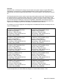
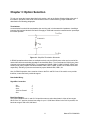
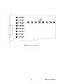
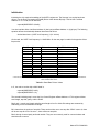
10623 Roselle Street, San Diego, CA 92121 • (858) 550-9559 • FAX (858) 550-7322
[email protected] • www.accesio.com
MODEL PCI-COM422/8
USER MANUAL
FILE: MPCI-COM422-8.D1g
Notice
The information in this document is provided for reference only. ACCES does not assume any liability
arising out of the application or use of the information or products described herein. This document may
contain or reference information and products protected by copyrights or patents and does not convey
any license under the patent rights of ACCES, nor the rights of others.
IBM PC, PC/XT, and PC/AT are registered trademarks of the International Business Machines
Corporation.
Printed in USA. Copyright 1995, 2005 by ACCES I/O Products Inc, 10623 Roselle Street, San Diego, CA
92121. All rights reserved.
WARNING!!
ALWAYS CONNECT AND DISCONNECT YOUR FIELD CABLING WITH
THE COMPUTER POWER OFF. ALWAYS TURN COMPUTER POWER
OFF BEFORE INSTALLING A CARD. CONNECTING AND
DISCONNECTING CABLES, OR INSTALLING CARDS INTO A SYSTEM
WITH THE COMPUTER OR FIELD POWER ON MAY CAUSE DAMAGE
TO THE I/O CARD AND WILL VOID ALL WARRANTIES, IMPLIED OR
EXPRESSED.
2
Manual PCI-COM422/8
Warranty
Prior to shipment, ACCES equipment is thoroughly inspected and tested to applicable specifications.
However, should equipment failure occur, ACCES assures its customers that prompt service and support
will be available. All equipment originally manufactured by ACCES which is found to be defective will be
repaired or replaced subject to the following considerations.
Terms and Conditions
If a unit is suspected of failure, contact ACCES' Customer Service department. Be prepared to give the
unit model number, serial number, and a description of the failure symptom(s). We may suggest some
simple tests to confirm the failure. We will assign a Return Material Authorization (RMA) number which
must appear on the outer label of the return package. All units/components should be properly packed for
handling and returned with freight prepaid to the ACCES designated Service Center, and will be returned
to the customer's/user's site freight prepaid and invoiced.
Coverage
First Three Years: Returned unit/part will be repaired and/or replaced at ACCES option with no charge for
labor or parts not excluded by warranty. Warranty commences with equipment shipment.
Following Years: Throughout your equipment's lifetime, ACCES stands ready to provide on-site or in-plant
service at reasonable rates similar to those of other manufacturers in the industry.
Equipment Not Manufactured by ACCES
Equipment provided but not manufactured by ACCES is warranted and will be repaired according to the
terms and conditions of the respective equipment manufacturer's warranty.
General
Under this Warranty, liability of ACCES is limited to replacing, repairing or issuing credit (at ACCES
discretion) for any products which are proved to be defective during the warranty period. In no case is
ACCES liable for consequential or special damage arriving from use or misuse of our product. The
customer is responsible for all charges caused by modifications or additions to ACCES equipment not
approved in writing by ACCES or, if in ACCES opinion the equipment has been subjected to abnormal
use. "Abnormal use" for purposes of this warranty is defined as any use to which the equipment is
exposed other than that use specified or intended as evidenced by purchase or sales representation.
Other than the above, no other warranty, expressed or implied, shall apply to any and all such equipment
furnished or sold by ACCES.
3
Manual PCI-COM422/8
Table of Contents
Chapter 1: Introduction .............................................................................................................................. 5
Specifications.......................................................................................................................................... 6
Figure 1-1: Block Diagram(Only one serial channel shown) ............................................................... 7
Chapter 2: Installation ................................................................................................................................ 8
Chapter 3: Option Selection..................................................................................................................... 11
Figure 3-1: Simplified Termination Schematic .................................................................................. 11
Figure 3-2: Option Selection Map...................................................................................................... 12
Figure 3-3: Low-Profile Option Selection Map .................................................................................. 13
Chapter 4: Address Selection.................................................................................................................. 14
Chapter 5: Programming .......................................................................................................................... 15
Table 5-1: Baud Rate Divisor Values................................................................................................. 16
Chapter 6: Connector Pin Assignments ................................................................................................. 19
Table 6-1: Connection Pin Assignments ........................................................................................... 19
Table 6-2: Data Cable Wiring ............................................................................................................ 20
4
Manual PCI-COM422/8
Chapter 1: Introduction
The Serial Interface Card was designed for effective transmission in RS422 (EIS422) protocol. The card
is 7.83 inches long and may be installed in PCI-bus slots of IBM PC or compatible computers. The card
features eight independent, asynchronous RS422 serial ports, type 16550 buffered UARTs.
RS422 Balanced Mode Operation
The card supports RS422 communications and uses differential balanced drivers for long range and
noise immunity. It also has the capability to add load resistors to terminate the communications lines.
RS422 communications requires that a transmitter supply a bias voltage to ensure a known "zero" state.
Also, receiver inputs at each end of the network should be terminated to eliminate "ringing". The card
supports biasing by default and supports termination by jumpers on the card. If your application requires
the transmitter to be un-biased, please contact the factory.
COM Port Compatibility
Type 16550 UARTs are used as the Asynchronous Communication Element (ACE). These include a 16byte transmit/receive buffer to protect against lost data in multitasking operating systems, while
maintaining 100% compatibility with the original IBM serial port. The system assigns the address(es).
A crystal oscillator is located on the card. This oscillator permits precise selection of baud rates up to
115,200 or, by changing a jumper, up to 921,600 with the standard crystal oscillator.
The driver/receiver used, the SN75176B, is capable of driving extremely long communication lines at high
baud rates. It can drive up to +60 mA on balanced lines and receive inputs as low as 200 mV differential
signal superimposed on common mode noise of +12 V or -7 V. In case of communication conflict, the
driver/receivers feature thermal shutdown.
Communication Mode
The card supports Full-Duplex and Half-Duplex communications with a 4-wire cable connection. HalfDuplex allows traffic to travel in both directions, but only one way at a time.
Baud Rate Ranges
The card has capability for two baud rate range selections and can be selected through the setting of the
CLK X1/CLK X4 jumper. The baud rates are selected on a port-by-port basis. One range is for up to
115,200 baud applications and the other is up to 921,600 baud applications. The lower baud rate is
selected when the jumper is in the CLK X1 position. When the jumper is in the X1 position we can utilize
the industry standard baud rate selection methodology. When in the X4 position, we must compensate for
the new input frequency by letting the Windows operating system see the frequency at 1/4 of the selected
value.
As an example when the X4 position is selected, assume the selected baud output is to be 9600 baud.
The operating system would need to have defined the value of 2400 baud so that the correct system
operations occur.
Note: Refer to the Baud Rate Divisor Value Table in chapter 5 of the manual.
5
Manual PCI-COM422/8
Specifications
Communications Interface
•
I/O Connection:
50-pin SCSI D-Connector
•
Serial Ports:
Eight cable terminated shielded male D-sub 9-pin with
standard IBM AT Style connectors compatible with
RS422 specifications.
•
Character length:
5, 6, 7, or 8 bits.
•
Parity:
Even, odd or none.
•
Stop Interval:
1, 1.5, or 2 bits.
•
Serial Data Rates:
Up to 115,200 baud, Asynchronous, A faster range of
rates, up to 921,600, is achieved by jumper selection on
the card. Type 16550 buffered UART.
•
Address:
Continuously mappable within 0000 to FFFF (hex) range
of PCI bus addresses.
•
Receiver Input Sensitivity:
+200 mV, differential input.
•
Common Mode Rejection:
+12V to -7V
•
Transmitter Output Drive Capability:
60 mA, with thermal shutdown.
Environmental
•
Operating Temperature Range: 0 °C. to +60 °C.
•
Storage temperature Range:
-50 °C. to +120 °C.
•
Humidity:
5% to 95%, non-condensing.
•
Power Required:
+5VDC at 125 mA typical, -12VDC at 5 mA typical,
+12VDC at 5 mA typical, 750 mW total power
consumption.
•
Size:
7.8 Inches long (198 mm) by 3.8 inches high (97 mm).
6
Manual PCI-COM422/8
DB50M
Figure 1-1: Block Diagram(Only one serial channel shown)
7
Manual PCI-COM422/8
Chapter 2: Installation
A printed Quick-Start Guide (QSG) is packed with the card for your convenience. If you’ve already
performed the steps from the QSG, you may find this chapter to be redundant and may skip forward to
begin developing your application.
The software provided with this card is on CD and must be installed onto your hard disk prior to use. To
do this, perform the following steps as appropriate for your operating system.
Configure Card Options via Jumper Selection
Before installing the card into your computer, carefully read Chapter 3: Option Selection of this manual,
then configure the card according to your requirements and protocol (RS-232, RS-422, RS-485, 4-wire
485, etc.). Our Windows based setup program can be used in conjunction with Chapter 3 to assist in
configuring jumpers on the card, as well as provide additional descriptions for usage of the various card
options (such as termination, bias, baud rate range, RS-232, RS-422, RS-485, etc.).
CD Software Installation
The following instructions assume the CD-ROM drive is drive “D”. Please substitute the appropriate drive
letter for your system as necessary.
DOS
1.
2.
3.
4.
Place the CD into your CD-ROM drive.
Type B- to change the active drive to the CD-ROM drive.
Type GLQR?JJ- to run the install program.
Follow the on-screen prompts to install the software for this board.
WINDOWS
1.
Place the CD into your CD-ROM drive.
2.
The system should automatically run the install program. If the install program does not run
promptly, click START | RUN and type BGLQR?JJ, click OK or press -.
3.
Follow the on-screen prompts to install the software for this board.
LINUX
1.
Please refer to linux.htm on the CD-ROM for information on installing under linux.
Note: COM boards can be installed in virtually any operating system. We do support installation in earlier
versions of Windows, and are very likely to support future versions as well.
Caution! * ESD A single static discharge can damage your card and cause premature
failure! Please follow all reasonable precautions to prevent a static
discharge such as grounding yourself by touching any grounded
surface prior to touching the card.
8
Manual PCI-COM422/8
Hardware Installation
1.
2.
3.
4.
5.
6.
7.
8.
9.
10.
11.
Make sure to set switches and jumpers from either the Option Selection section of this manual or
from the suggestions of SETUP.EXE.
Do not install card into the computer until the software has been fully installed.
Turn OFF computer power AND unplug AC power from the system.
Remove the computer cover.
Carefully install the card in an available 5V or 3.3V PCI expansion slot (you may need to remove
a backplate first).
Inspect for proper fit of the card and tighten screws. Make sure that the card mounting bracket is
properly screwed into place and that there is a positive chassis ground.
Install an I/O cable onto the card’s bracket mounted connector.
Replace the computer cover and turn ON the computer. Enter the CMOS setup program of your
system and verify that the PCI plug-and-play option is set appropriately for your system. Systems
running Windows 95/98/2000/XP/2003 (or any other PNP-compliant operating system) should set
the CMOS option to OS. Systems running under DOS, Windows NT, Windows 3.1, or any other
non-PNP-compliant operating system should set the PNP CMOS option to BIOS or Motherboard.
Save the option and continue booting the system.
Most computers should auto-detect the card (depending on the operating system) and
automatically finish installing the drivers.
Run PCIfind.exe to complete installing the card into the registry (for Windows only) and to
determine the assigned resources.
Run one of the provided sample programs that was copied to the newly created card directory
(from the CD) to test and validate your installation.
The base address assigned by BIOS or the operating system can change each time new hardware is
installed into or removed from the computer. Please recheck PCIFind or Device Manager if the hardware
configuration is changed. Software you write can automatically determine the base address of the card
using a variety of methods depending on the operating system. In DOS, the PCI\SOURCE directory
shows the BIOS calls used to determine the address and IRQ assigned to installed PCI devices. In
Windows, the Windows sample programs demonstrate querying the registry entries (created by PCIFind
and NTIOPCI.SYS during boot-up) to determine this same information.
9
Manual PCI-COM422/8
Interrupts
Please note that, in Windows NT, changes must be made to the system registry to support IRQ sharing.
The following is excerpted from "Controlling Multiport Serial I/O Cards" provided by Microsoft in the
MSDN library, documentid:mk:@ivt:nt40res/D15/S55FC.HTM, also available in the WindowsNT Resource
Kit.
The Microsoft serial driver can be used to control many dumb multiport serial cards. Dumb indicates that
the control includes no on-board processor. Each port of a multiport card has a separate subkey under
the HKLM\CurrentControlSet\Services\Serial\Parameters subkey in the registry. In each of these subkeys,
you must add values for DosDevices, Interrupt, InterruptStatus, PortAddress, and PortIndex because
these are not detected by the Hardware Recognizer. (For descriptions and ranges for these values, see
Regentry.hlp, the Registry help file on the WindowsNT Workstation Resource Kit CD.)
For example, if you have an eight-port card configured to use address 0xFC00 with an interrupt of 05, the
values in the Registry are:
Serial##### Subkey:
PortAddress = REG_DWORD 0xFC00
Interrupt = REG_WORD 5
DosDevices = REG_SZ COM5
InterruptStatus = REG_DWORD 0xFC40
PortIndex = REG_DWORD 1
Serial##### Subkey:
PortAddress = REG_DWORD 0xFC00
Interrupt = REG_WORD 5
DosDevices = REG_SZ COM5
InterruptStatus = REG_DWORD 0xFC40
PortIndex = REG_DWORD 1
Serial##### Subkey:
PortAddress = REG_DWORD 0xFC08
Interrupt = REG_DWORD 5
DosDevices = REG_SZ COM6
InterruptStatus = REG_DWORD 0xFC40
PortIndex = REG_DWORD 2
Serial##### Subkey:
PortAddress =_DWORD 0xFC10
Interrupt = REG_DWORD 5
DosDevices = REG_SZ COM7
InterruptStatus = REG_DWORD 0xFC40
PortIndex - REG_DWORD 3
Serial##### Subkey:
PortAddress = REG_DWORD 0xFC18
Interrupt = REG_DWORD 5
Dos Devices = REG_SZ COM8
InterruptStatus = REG_DWORD 0xFC40
PortIndex = REG_DWORD4
Serial##### Subkey:
PortAddress = REG_DWORD 0xFC20
Interrupt = REG_DWORD 5
DosDevices = REG_SZ COM9
InterruptStatus = REG_DWORD 0xFC40
PortIndex - REG_DWORD 5
Serial##### Subkey:
PortAddress = REG_DWORD 0xFC20
Interrupt = REG_DWORD 5
DosDevices = REG_SZ COM9
InterruptStatus = REG_DWORD 0xFC40
PortIndex - REG_DWORD 5
Serial##### Subkey:
PortAddress = REG_DWORD 0xFC28
Interrupt = REG_DWORD 5
DosDevices = REG_SZ COM10
InterruptStatus = REG_DWORD 0xFC40
PortIndex = REG_DWORD 6
Serial##### Subkey:
PortAddress = REG_DWORD 0xFC30
Interrupt = REG_DWORD 5
DosDevices = REG_SZ COM11
InterruptStatus = REG_DWORD 0xFC40
PortIndex = REG_DWORD 7
Serial##### Subkey:
PortAddress = REG_DWORD 0xFC38
Interrupt = REG_DWORD 5
DosDevices = REG_SZ COM12
InterruptStatus = REG_DWORD 0xFC40
PortIndex = REG_DWORD8
As this example shows, the shared IRQ status Register is located at Base address + 0x40.
10
Manual PCI-COM422/8
Chapter 3: Option Selection
To help you locate the jumpers described in this section, refer to the Option Selection Map at the end of
this section. Operation of the serial communications section is determined by jumper installation as
described in the following paragraphs.
Terminations
A transmission line should be terminated at the receiving end in its characteristic impedance. Installing a
jumper at the locations labeled LDxO and LDxI apply a 120Ω load across the transmit/receive input/output
for RS422 operation.
Tx+/R x+
COM422LD
120
0.1 :F
Tx-/R xFigure 3-1: Simplified Termination Schematic
In RS422 operations where there are multiple terminals, only the RS422 ports at the receiver end of the
network should have terminating impedance as described above. To so terminate the COM A port, place
a jumper at the location labeled LDAO. To terminate the COM B, COM C, COM D, COM E, COM F and
COM H ports, place jumpers at locations labeled LDBO, LDCO, LDDO, LDEO, LDFO LDGO and LDHO
respectively. Similarly, Inputs are terminated at jumpers labeled LDAI, LDB1, etc.
Also, for RS422 operation, there must be a bias on the RX+ and RX- lines. If the card is not to provide
that bias, contact the factory technical support.
Data Cable Wiring
SignalPin Connection
AinAout+
Aout100 Ω to Ground
Ain+
1
2
3
5
9
Baud Rate Ranges
The jumpers labeled CLK X1 and CLK X4 provide means to select baud rates in either of two ranges.
When in the "X1" position, the baud rate range is up to 115,200 baud. When in the CLK X4 position, the
baud rate range is 200 to 921,600 baud.
11
Manual PCI-COM422/8
Figure 3-2: Option Selection Map
12
Manual PCI-COM422/8
Figure 3-3: Low-Profile Option Selection Map
13
Manual PCI-COM422/8
Chapter 4: Address Selection
The card uses one address space. COM A, COM B, COM C, COM D, COM E, COM F, COM G, and
COM H each occupy eight consecutive register locations. The interrupt register which indicates which port
or ports caused the interrupt is located at base address + 64.
PCI architecture is Plug-and-Play. This means that the BIOS or Operating System determines the
resources assigned to PCI cards rather than you selecting those resources with switches or jumpers. As a
result, you cannot set or change the card's base address. You can only determine what the system has
assigned.
To determine the base address that has been assigned, run the PCIFind.EXE, or PCINT utility program
provided. This utility will display a list of all of the cards detected on the PCI bus, the addresses assigned
to each function on each of the cards, and the respective IRQs (if any) allotted.
Alternatively, some operating systems (Windows95/98/2000) can be queried to determine which
resources were assigned. In these operating systems, you can use either PCIFind (DOS) or PCINT
(Windows95/98/NT), or the Device Manager utility from the System Applet of the control panel. The PCICOM422/8 is installed in the Data Acquisition class of the Device Manager list. Selecting the card,
clicking Properties, and then selecting the Resources Tab will display a list of the resources allocated to
the card.
The PCI bus supports 64K of I/O space, so your card's addresses may be located anywhere in the 0000
to FFFF hex range.
Vendor ID code is 494F (ASCII for "I/O")
Device ID code is 1068
14
Manual PCI-COM422/8
Chapter 5: Programming
Sample Programs
There are sample programs provided with the card in C, Pascal, QuickBASIC, and several Windows
languages. DOS samples are located in the DOS directory and Windows samples are located in the
WIN32 directory.
Windows Programming
The card installs into Windows as COM ports. Thus the Windows standard API functions can be used. In
particular:
►
CreateFile() and CloseHandle() for opening and closing a port.
►
SetupComm(), SetCommTimeouts(), GetCommState(), and SetCommState() to set and
change a port’s settings.
►
ReadFile() and WriteFile() for accessing a port.
See the documentation for your chosen language for details.
Under DOS, the process is very different. The remainder of this chapter describes DOS programming.
15
Manual PCI-COM422/8
Initialization
Initializing the chip requires knowledge of the UART's register set. The first step is to set the baud rate
divisor. You do this by first setting the DLAB (Divisor Latch Access Bit) high. This bit is Bit 7 at Base
Address +3. In C code, the call would be:
outportb(BASEADDR +3,0x80);
You then load the divisor into Base Address +0 (low byte) and Base Address +1 (high byte). The following
equation defines the relationship between baud rate and divisor:
desired baud rate = (UART clock frequency) / (32 * divisor)
On the card, the UART clock frequency is 1.8432 MHz. On the next page is a table for the popular divisor
frequencies.
Baud Rate
921600
460800
230400
153600
115200
57600
38400
28800
19200
14400
9600
4800
2400
1200
Divisor x1
1
2
3
4
6
8
12
24
48
96
Divisor x8
1
2
4
6
8
16
24
32
48
64
96 – Most Common
192
384
768
Max Diff. Cable Length*
250 ft
550 ft
1400 ft
2500 ft
3000 ft
4000 ft
4000 ft
4000 ft
4000 ft
4000 ft
4000 ft
4000 ft
4000 ft
4000 ft
* These are theoretical maximums for typical conditions and good quality cables based on the EIA 485 and EIA 422 standard for
balanced differential drivers.
Table 5-1: Baud Rate Divisor Values
In C, the code to set the chip to 9600 baud is:
outportb(BASEADDR, 0x0C);
outportb(BASEADDR +1,0);
The second initializing step is to set the Line Control Register at Base Address +3. This register defines
word length, stop bits, parity, and the DLAB.
Bits 0 and 1 control word length and allow word lengths from 5 to 8 bits. Bit settings are extracted by
subtracting 5 from the desired word length.
Bit 2 determines the number of stop bits. There can be either one or two stop bits. If Bit 2 is set to 0, there
will be one stop bit. If Bit 2 is set to 1, there will be two stop bits.
Bits 3 through 6 control parity and break enable. They are not commonly used for communications and
should be set to zeroes.
16
Manual PCI-COM422/8
Bit 7 is the DLAB discussed earlier. It must be set to zero after the divisor is loaded or else there will be
no communications.
The C command to set the UART for an 8-bit word, no parity, and one stop bit is:
outportb(BASEADDR +3, 0x03)
Reception
Reception can be handled in two ways: polling and interrupt-driven. When polling, reception is
accomplished by constantly reading the Line Status Register at Base Address +5. Bit 0 of this register is
set high whenever data are ready to be read from the chip. A simple polling loop must continuously check
this bit and read in data as it becomes available. The following code fragment implements a polling loop
and uses a value of 13, (ASCII Carriage Return) as an end-of-transmission marker:
do
{
while (!(inportb(BASEADDR +5) & 1));
data[i++]= inportb(BASEADDR);
}
while (data[i]!=13);
/*Wait until data ready*/
/*Reads the line until null character rec'd*/
Interrupt-driven communications should be used whenever possible and is required for high data rates.
Writing an interrupt-driven receiver is not much more complex than writing a polled receiver but care
should be taken when installing or removing your interrupt handler to avoid writing the wrong interrupt,
disabling the wrong interrupt, or turning interrupts off for too long a period.
The handler would first read the Interrupt Identification Register at Base Address +2. If the interrupt is for
Received Data Available, the handler then reads the data. If no interrupt is pending, control exits the
routine. A sample handler, written in C, is as follows:
readback = inportb(BASEADDR +2);
if (readback & 4)
data[i++]=inportb(BASEADDR);
outportb(0x20,0x20);
return;
/*Readback will be set to 4 if data are available*/
/*Write EOI to 8259 Interrupt Controller*/
17
Manual PCI-COM422/8
Transmission
To transmit a string of data, the transmitter must first check Bit 5 of the Line Status Register at Base
Address +5. That bit is the transmitter-holding-register-empty flag. If it is high, the transmitter has sent the
data. The process of checking the bit until it goes high followed by a write is repeated until no data
remains.
The following C code fragment demonstrates this process:
while(data[i]);
{
while(!(inportb(BASEADDR +5)&0x20));
outportb(BASEADDR,data[i]);
i++;
}
/*While there is data to send*/
/*Wait until transmitter is empty*/
18
Manual PCI-COM422/8
Chapter 6: Connector Pin Assignments
Input/Output Connections
The card uses a 50-pin SCSI D-connector to interface to a spider cable. The spider cable has eight
individual 9-pin connectors provided with it.
To ensure that there is minimum susceptibility to EMI and minimum radiation it is important that the card
mounting bracket be properly screwed into place and that there be a positive chassis ground. Also,
proper EMI cabling techniques (cable connect to chassis ground at the aperture, shielded twisted-pair
wiring, etc) must be used for the input/output wiring.
Pin RS-422 Signals
Pin RS-422 Signals
1
GND
Ground
26 GND
2
Aout+
27 Eout+
3
Aout-
28 Eout-
4
Ground through 100 Ohm R
29 Ground through 100 Ohm R
5
Ain+
30 Ein+
6
Ain-
31 Ein-
7
GND
8
Bout+
33 Fout+
9
Bout-
34 Fout-
10
Ground through 100 Ohm R
35 Ground through 100 Ohm R
11
Bin+
36 Fin+
12
Bout-
37 Fout-
13
GND
14
Cout+
39 Gout+
15
Cout-
40 Gout-
16
Ground through 100 Ohm R
41 Ground through 100 Ohm R
17
Cin+
42 Gin+
18
Cin-
43 Gin-
19
GND
20
Dout+
45 Hout+
21
Dout-
46 Hout-
22
Ground through 100 Ohm R
47 Ground through 100 Ohm R
23
Din+
48 Hin+
24
Din-
49 Hin-
25
GND
Ground
32 GND
Ground
38 GND
Ground
44 GND
Ground
50 GND
Ground
Ground
Ground
Ground
Ground
Table 6-1: Connection Pin Assignments
19
Manual PCI-COM422/8
Signal
Connector Pin
Ain-
Pin 1
Aout+
Pin 2
Aout-
Pin 3
100 Ohm to Ground Pin 5
Ain+
Pin 9
Table 6-2: Data Cable Wiring
20
Manual PCI-COM422/8
Customer Comments
If you experience any problems with this manual or just want to give us some feedback, please email us
at: [email protected]. Please detail any errors you find and include your mailing address so that
we can send you any manual updates.
10623 Roselle Street, San Diego CA 92121
Tel. (858)550-9559 FAX (858)550-7322
www.accesio.com
21
Manual PCI-COM422/8