1
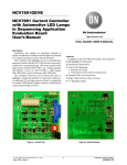
Preliminary Information
NCV7691RCLEVB
NCV7691 8-channel Rear
Combo / Daylight Running
Light Evaluation Board User’s
Manual
http://onsemi.com
EVAL BOARD USER’S MANUAL
Prepared by: Ondrej Kupcik
Updated by: Ladislav Bažant
ON Semiconductor
Introduction
The evaluation board demonstrates rear combination / daylight running
light (RCL/DRL) solution with up to eight LED string. The board
regulates constant current of 100 mA (68 to 150 mA) through each onboard LED string consisting of three red or two white LEDs in the wide
range of the supply voltage. The current is reduced for the board
temperature above 90°C. The board is designed in order to provide
good cooling of the active components with no extra cost. Additionally,
a heat sink may be mounted on the bottom side of the board to improve
the thermal capability of the board. In case of LEDs short or opening,
the current sources are disabled and the fault may be detected by the
ECU diagnostics.
On-board LEDs may be easily replaced by external ones.
Evaluation Board Features
•
•
•
•
•
•
•
•
•
•
•
•
Wide range of supply voltage: 7 to 40 V
Eight LED strings with on-board red or white LEDs (RCL/DRL)
Nominal LED current 100 mA (150 mA max.)
Over-temperature current fold-back protection
OPEN jumper in each string allowing LEDs disconnection
SHORT jumper in each string for short emulation or connection of
the external LEDs
Led short-circuit and open-load emulation jumpers
Optional external PWM input
Optional Error flagging through indication LED and FLTS output
Positions for optional EMC capacitors
One-side components assembly
Passive cooling (optional heat sink may be attached to the bottom)
© Semiconductor Components Industries, LLC, 2015
May, 2015 – Rev i2.10
http://onsemi.com
EVBUMXXXX
Publication Order Number:
Figure 1: Running NCV7691 Evaluation Board Picture
Table 1. Absolute Maximum Ratings
Rating
Supply Voltage (Vbat)
LED String Current (thermally limited)
PWM, FLTS, Err Voltage (J1 connector)
Error pin current (J1 connector, pin 3)
Junction Temperature (NCV7691, BCP56)
Junction Temperature (ASMT-QRBD-AEF0E, ASMT-QWBF-NKL0E)
Ambient Temperature
Value
-40 to +40
150
-0.3 to Vbat
0 to 200
-40 to +150
-40 to +125
-40 to +105
Unit
V
mA
V
mA
°C
°C
°C
Table 2. Recommended Board Operating Conditions
Rating
Supply Voltage (Vbat)
Rated LED string Current (VS < 18 V, Tboard < +90°C)
Open-Load or Short-Circuit board consumption (VS = 14 V)
Ambient Temperature (for rated LED current)
Value
7 to 18
68 /100 /150
max. 7
-40 to +70
Unit
V
mA
mA
°C
Preliminary Information
Rear Combo / Daylight Running Light Evaluation Board Schematic
Figure 2: NCV7691 RCL/DRL Evaluation Board Schematic
http://onsemi.com
3
Preliminary Information
Table 3. Interface Function Description
Connector Name
VBAT
OPEN1-8
Connector Type
2.1 mm DC supply
SMD Jumper
SHORT1-8
SMD Jumper
B
Col1
Col5
FB
FB1
FB5
Test Point
Test Point
Test Point
Test Point
Test Point
Test Point
J1
SMD Header
Description / Function
Supply battery input
Removing the jumper emulates open LED condition
Shorting terminals by the jumper emulates short LED condition OR
terminal for external LEDs
BASE output of NCV7691 / NPN base
String 1 NPN collector
String 5 NPN collector
FB output of NCV7691
String 1 NPN emitter / feedback resistor
String 5 NPN emitter / feedback resistor
Control/diagnostic functions:
Pin 1: GND
Pin 2: PWM input (10k pull-up to VS)
Pin 3: Error signal (active low, pull-up to VS through LED and 10k)
Pin 4: FLTS pin of NCV7691
Pin 5: Alternative pull-up input for the error signal (if used, remove R9’)
Getting Started
The board is supplied through a standard 5.5 x 2.1 mm
DC connector. Nominal supply voltage ranges from 7 to
18 V. Below 7 V, the current through the LEDs starts
decreasing. For battery voltage above 18 V, the LED
current is reduced by the over-voltage fold back to reduce
the power dissipation.
The thermal fold-back circuitry ensures the board
temperature remains within the safe range (see following
chapter for details).
Two jumpers in each string emulate LEDs short or
opening. By default, OPEN jumper is closed while SHORT
terminals are not shorted. Alternatively, external LEDs may
be connected through SHORT header while on-board LEDs
are disconnected.
7 to 18 V
2.1 mm DC supply
The LEDs current is defined by Rx1 resistors. By default,
it is set to 100 mA, but may be changed using following
formula:
•
•
With no thermal fold-back (NTC pin grounded):
𝐹𝐹𝐹𝐹 𝑅𝑅𝑅𝑅𝑅𝑅𝑅𝑅𝑙𝑙𝑙𝑙𝑙𝑙𝑙𝑙𝑙𝑙𝑙𝑙 𝑉𝑉𝑉𝑉𝑉𝑉𝑉𝑉𝑉𝑉𝑉𝑉𝑉𝑉 0.15
𝑅𝑅1 =
≈
𝐼𝐼𝐿𝐿𝐿𝐿𝐿𝐿
𝐼𝐼𝐿𝐿𝐿𝐿𝐿𝐿
With thermal fold-back circuitry on NTC pin:
𝑉𝑉𝑁𝑁𝑁𝑁𝑁𝑁
1.5
0.15
𝑅𝑅1 =
≈
=
10 ∙ 𝐼𝐼𝐿𝐿𝐿𝐿𝐿𝐿 10 ∙ 𝐼𝐼𝐿𝐿𝐿𝐿𝐿𝐿 𝐼𝐼𝐿𝐿𝐿𝐿𝐿𝐿
LED current programming resistors
Thermal fold-back circuitry
NCV7691
Positions for optional EMC resistors
Figure 3: NCV7691 8-channel Evaluation Board Picture
Modules control strategy
The board is designed to operate in standard “One Wire
Driver Body ECU” and decentralized architecture.
In the first case, both control and diagnosis is done
through one supply wire. The dimming might be provided
through the PWM applied to the High-side SmartFET in the
body ECU. At the same time, the SmartFET allows
diagnosis of the failure on the LED module (open load or
short-circuit) (see Figure 3). In case of both LED short and
disconnection, NCV7691 disables all the NPN bipolars.
In decentralized operation, extra wires are needed for the
control and diagnosis (Figure 4). For this purpose, header
J1 is available on the board for easy access to FLTS and
PWM functions of NCV7691.
http://onsemi.com
4
Preliminary Information
Normal operation
LED string open
LED string short
ECU
ECU
ECU
control
diagnostics
control
control
diagnostics
NCV8460A
RCL / DRL
7 mA max.
@ 14 V
RCL / DRL
open
8x 100 mA
NCV7691
NCV8460A
7 mA max.
@ 14 V
0.8 A
RCL / DRL
diagnostics
NCV8460A
short
NCV7691
NCV7691
Figure 4: Centralized One Wire System Diagram
Normal operation
LED string open
LED string short
ECU
ECU
ECU
Control / diagnostics
Control / diagnostics
Control / diagnostics
error
RCL / DRL
error
RCL / DRL
RCL / DRL
open
NCV7691
NCV7691
Figure 5: De-centralized System Diagram
http://onsemi.com
5
short
NCV7691
Preliminary Information
Open LED string diagnostics
VS
NCV7691 includes Open Load Detection feature. When
the LED is open, the control loop tries to increase the BASE
current to reach 152 mV on the FB pin. As the BASE
current is limited to typ. 25 mA, the FB voltage drops below
the target level. When the FB voltage decreases below the
Open Load Detection FB Threshold (typ. 75 mA), an open
load is detected after a period defined by a capacitor
connected to the FLTS pin. Figure 5 demonstrates an open
load situation on two-string application.
V(SC) > (VS - 2 V) ->
-> FLTS curre nt source active
-> LEDs o ff
VS-0.5V
BCP56
BCP56
NCV7691
1R5
1R5
SC
BAS E
FB
GND
BCP56
~24.8mA
~0.2mA
90mV
NCV7691
SC
BCP56
37.2mV
1R5
60mA
25mA
Figure 8: Short LED detection principle
1R5
Thermal considerations of the board
24.8mA
BAS E
FB
GND
63.6mV
V(FB) < 75 mV ->
-> FLTS curre nt source active ->
-> LEDs o ff
Figure 6: Open load detection principle
In multi-string applications with high-beta transistors, the
feedback voltage from individual strings is averaged, so one
defective LED string does not always lead to the open load
detection.
One of the ways to improve the open load detection
capability is more precise external BASE current limitation.
An example of the circuit with one extra resistor and PNP
bipolar is shown in Figure 6.
As the board dissipation is typ. 11 W at 13.8 V battery
supply and 100 mA LED current, the thermal aspects
should be taken into account for the board design. The main
limitations are LED lifetime vs. operating temperature and
NPN bipolar maximum junction temperature.
The board was designed to operate at full current with
board temperature of up to 90°C on standard 70 μm FR4
PCB substrate and passive cooling without any extra
thermal improvements. In case higher power dissipation is
foreseen, a cooling metal profile may be mounted to the
bottom side of the board,
Thermal fold-back
To the protect power dissipating devices on the board
(LEDs, NPN bipolar transistor), a circuit reducing LED
current at high board temperatures is included (Figure 8).
VS
R3
10k
BCP56
~9.3mA
~0.1mA
NCV7691 ~10mA
R4
100k
45mV
47R
1R5
30mA
1R5
4V7
10.9mA
R5
51k
57.3mV
GND
BC856
R6
560k
PTC
to NTC pin
BAS E
FB
Temperature
dependent
element
Voltage reference
14mV
max.
SC
~4.3 V
BCP56
V(FB) < 75 mV ->
-> FLTS curre nt source active ->
-> LEDs o ff
T < Tsense: 470 Ω
T = Tsense + 15°C: >40 kΩ
Figure 9: Thermal fold-back circuitry
Figure 7: Improved open load detection for 8 strings
Short LED diagnostics
NCV7691 contains a LED string short detection based on
LED string voltage measurement (pin SC). In case the
voltage difference between the VS and SC pins drops below
typ. 2 V (Figure 7), the BASE is switched off and FLTS
current source is active to flag an error. In multi-string
applications, an OR-circuitry (e.g. diodes) has to be used to
cover all the strings.
The circuit consists of a voltage reference (ZD1 supplied
via R3) and temperature dependent resistor divider. A
thermistor with positive temperature dependency (PTC) is
used for temperature sensing. For temperatures below the
PTC sensing temperature, the thermistor has low resistance
(typ. 470 Ω), so the circuitry output voltage is given by R4
and R5 while for high temperatures the reference voltage
drops rapidly (Figure 9). R6 ensures the voltage on NTC
input does not fall below the NTC Detection Level (max.
300 mV) at high temperature, which would result into a
switch-over to the internal voltage reference of NCV7691.
http://onsemi.com
6
Preliminary Information
4.3 V
4.3 V
R4
100k
T < Tsense
R4
100k
R6
560k
PTC ~ 470R
R6
560k
1.45 V to NTC pin
0.31 V to NTC pin
R5 V(NTC) has to be > 0.3 V
R5
51k
T >> Tsense
PTC → ∞
The sensing temperature (PTC parameter) has to be
chosen carefully with respect to the heat distribution over
the board and thermal properties of the power dissipating
components. For PTC type B59641A95A62, the current
fold-back reduces the reference voltage on the NTC pin and
thus LED current above the board temperature of ~90°C
(Figure 11).
51k
Figure 10: Thermal fold-back circuitry at low / high
temperature
The optimal Zener voltage in terms of the temperature
independency is usually between 4 and 5 V. At the same
time, it should be as low as possible to allow a low-battery
operation. 4V7 Zener diode is recommended as a good
tradeoff. Because of lower bias current (< 1 mA) and
impedance of the Zener, the reference voltage is lower than
the nominal one (~4.3 V for 4V7 Zener) (Figure 10).
Figure 12: NTC voltage vs. board temperature (VS=12V)
If the thermal fold-back feature is not required,
components R3, R4, R6, ZD1 and PTC do not need to be
assembled and NTC pin should be tied to GND (directly or
via R5).
EMC recommendations
Figure 11: NTC voltage vs. supply voltage (Tpcb = 25°C)
If extensive EMC immunity level is required, Cx1, C3 and
C4 capacitors can improve the EMC performance. Using C3
is usually sufficient against disturbances from the supply
line. Capacitors Cx1 and C4 may further improve the
performance esp. in the setups with external (off-board)
LEDs.
http://onsemi.com
7
Preliminary Information
PCB Drawings
Assembly Drawings
Figure 13: NCV7691 RCL EVB PCB Top Assembly Drawing (Red LEDs) Option A
Figure 14: NCV7691 DRL EVB PCB Top Assembly Drawing (White LEDs) Option B
Composite Drawings
Figure 15: NCV7691 RCL/DRL EVB PCB Top Composite Drawing
http://onsemi.com
8
Preliminary Information
Figure 16: NCV7691 RCL/DRL EVB PCB Bottom Composite Drawing
http://onsemi.com
9
Preliminary Information
REFERENCES
[1]
[2]
[3]
ON Semiconductor, NCV7691 Product Datasheet Rev. 2, January 2015.
EPCOS, PTC thermistors as limit temperature sensors, Series: B59421, B59641, B59721, March 2014
ON Semiconductor, BCP56 NPN Silicon Epitaxial Transistor, Rev. 10, March, 2014.
http://onsemi.com
10
Preliminary Information
ON Semiconductor and
are registered trademarks of Semiconductor Components Industries, LLC (SCILLC). SCILLC reserves the right to make
changes without further notice to any products herein. SCILLC makes no warranty, representation or guarantee regarding the suitability of its products for
any particular purpose, nor does SCILLC assume any liability arising out of the application or use of any product or circuit, and specifically disclaims any and
all liability, including without limitation special, consequential or incidental damages. “Typical” parameters which may be provided in SCILLC data sheets
and/or specifications can and do vary in different applications and actual performance may vary over time. All operating parameters, including “Typicals” must
be validated for each customer application by customer's technical experts. SCILLC does not convey any license under its patent rights nor the rights of
others. SCILLC products are not designed, intended, or authorized for use as components in systems intended for surgical implant into the body, or other
applications intended to support or sustain life, or for any other application in which the failure of the SCILLC product could create a situation where personal
injury or death may occur. Should Buyer purchase or use SCILLC products for any such unintended or unauthorized application, Buyer shall indemnify and
hold SCILLC and its officers, employees, subsidiaries, affiliates, and distributors harmless against all claims, costs, damages, and expenses, and reasonable
attorney fees arising out of, directly or indirectly, any claim of personal injury or death associated with such unintended or unauthorized use, even if such
claim alleges that SCILLC was negligent regarding the design or manufacture of the part. SCILLC is an Equal Opportunity/Affirmative Action Employer. This
literature is subject to all applicable copyright laws and is not for resale in any manner.
PUBLICATION ORDERING INFORMATION
Literature Fulfillment:
Literature Distribution Center for ON Semiconductor
P.O. Box 5163, Denver, Colorado 80217 USA
Phone: 303–675–2175 or 800–344–3860 Toll Free USA/Canada
Fax: 303–675–2176 or 800–344–3867 Toll Free USA/Canada
Email: [email protected]
JAPAN: ON Semiconductor, Japan Customer Focus Center
2–9–1 Kamimeguro, Meguro–ku, Tokyo, Japan 153–0051
Phone: 81–3–5773–3850
Email: [email protected]
N. American Technical Support: 800–282–9855 Toll Free USA/Canada
For additional information, please contact your local
Sales Representative.
ON Semiconductor Website: http://onsemi.com
http://onsemi.com
11


![LEGASIC IrCOMMアダプタPro Plus[ 137KB]](http://vs1.manualzilla.com/store/data/006589505_2-7f310eff1596309770aaa67c0dbcdaf0-150x150.png)