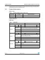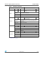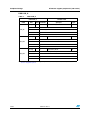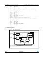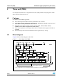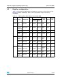
1
RM0148
Reference manual
ST40 core support peripherals (ST40-300)
Overview
Note:
This manual reflects the core support peripherals (CSP) for the ST40-300 series devices
only.
The ST40 CSP package contains a set of core support peripherals for use in ST40-based
system on chips (SoCs). These peripherals are designed to provide many common
functions used by embedded operating systems.
This manual provides details on the architecture of the core support peripherals which
includes: Clock, power and reset control (CPRC), Timer unit (TMU), User debug interface
(UDI) and the Interrupt controller (INTC).
This manual also describes the peripheral bridge which acts as the interface between the
peripherals and the STBus. This is achieved by grouping the modules into a single port on
the STBus, and handling any data size, data rate and endianness issues transparently.
For the architectural description of the peripheral bridge, see Chapter 2: Peripheral bridge
on page 9.
October 2011
8011247 Rev 5
1/58
www.st.com
Contents
ST40 core support peripherals (300 series)
Contents
1
Architectural overview . . . . . . . . . . . . . . . . . . . . . . . . . . . . . . . . . . . . . . . 7
2
Peripheral bridge . . . . . . . . . . . . . . . . . . . . . . . . . . . . . . . . . . . . . . . . . . . . 9
2.1
Address map . . . . . . . . . . . . . . . . . . . . . . . . . . . . . . . . . . . . . . . . . . . . . . . 9
2.1.1
Virtual addressing of a CPU’s own CSP peripherals . . . . . . . . . . . . . . . . 9
2.1.2
CSP physical addressing . . . . . . . . . . . . . . . . . . . . . . . . . . . . . . . . . . . . . 9
2.1.3
Error conditions . . . . . . . . . . . . . . . . . . . . . . . . . . . . . . . . . . . . . . . . . . . 10
2.2
Bridge registers . . . . . . . . . . . . . . . . . . . . . . . . . . . . . . . . . . . . . . . . . . . . 11
2.3
Peripheral subsystem access errors . . . . . . . . . . . . . . . . . . . . . . . . . . . . 11
2.3.1
3
Clock, power and reset control (CPRC) . . . . . . . . . . . . . . . . . . . . . . . . 15
3.1
Features . . . . . . . . . . . . . . . . . . . . . . . . . . . . . . . . . . . . . . . . . . . . . . . . . . 15
3.2
Register configuration . . . . . . . . . . . . . . . . . . . . . . . . . . . . . . . . . . . . . . . 16
3.3
Powerdown modes . . . . . . . . . . . . . . . . . . . . . . . . . . . . . . . . . . . . . . . . . . 16
3.4
3.5
3.6
2/58
Peripheral bridge registers . . . . . . . . . . . . . . . . . . . . . . . . . . . . . . . . . . . 12
3.3.1
Types of powerdown modes . . . . . . . . . . . . . . . . . . . . . . . . . . . . . . . . . 16
3.3.2
Module clock control register (CPRC.STBCR) . . . . . . . . . . . . . . . . . . . 18
3.3.3
Module clock control register 2 (CPRC.STBCR2) . . . . . . . . . . . . . . . . . 19
3.3.4
Sleep mode . . . . . . . . . . . . . . . . . . . . . . . . . . . . . . . . . . . . . . . . . . . . . . 20
Module clock-stop functions . . . . . . . . . . . . . . . . . . . . . . . . . . . . . . . . . . . 20
3.4.1
Timer unit (TMU) . . . . . . . . . . . . . . . . . . . . . . . . . . . . . . . . . . . . . . . . . . 20
3.4.2
User break controller stop function . . . . . . . . . . . . . . . . . . . . . . . . . . . . 20
Watchdog timer . . . . . . . . . . . . . . . . . . . . . . . . . . . . . . . . . . . . . . . . . . . . 22
3.5.1
Watchdog timer counter (WTCNT) . . . . . . . . . . . . . . . . . . . . . . . . . . . . 23
3.5.2
Watchdog timer control/status register (WTCSR) . . . . . . . . . . . . . . . . . 23
3.5.3
Watchdog timer control/status register 2 (WTCSR2) . . . . . . . . . . . . . . . 26
3.5.4
Notes on register access . . . . . . . . . . . . . . . . . . . . . . . . . . . . . . . . . . . . 26
Using the WDT . . . . . . . . . . . . . . . . . . . . . . . . . . . . . . . . . . . . . . . . . . . . . 27
3.6.1
Using watchdog timer mode . . . . . . . . . . . . . . . . . . . . . . . . . . . . . . . . . 27
3.6.2
Using interval timer mode . . . . . . . . . . . . . . . . . . . . . . . . . . . . . . . . . . . 27
8011247 Rev 5
ST40 core support peripherals (300 series)
4
Timer unit (TMU) . . . . . . . . . . . . . . . . . . . . . . . . . . . . . . . . . . . . . . . . . . . 28
4.1
Features . . . . . . . . . . . . . . . . . . . . . . . . . . . . . . . . . . . . . . . . . . . . . . . . . . 28
4.2
Block diagram . . . . . . . . . . . . . . . . . . . . . . . . . . . . . . . . . . . . . . . . . . . . . . 28
4.3
Register configuration . . . . . . . . . . . . . . . . . . . . . . . . . . . . . . . . . . . . . . . 29
4.4
Register descriptions . . . . . . . . . . . . . . . . . . . . . . . . . . . . . . . . . . . . . . . . 30
4.5
5
Contents
4.4.1
Timer start register (TMU.TSTR) . . . . . . . . . . . . . . . . . . . . . . . . . . . . . . 30
4.4.2
Timer constant registers (TMU.TCOR) . . . . . . . . . . . . . . . . . . . . . . . . . 31
4.4.3
Timer counters (TMU.TCNT) . . . . . . . . . . . . . . . . . . . . . . . . . . . . . . . . . 31
4.4.4
Timer control registers (TMU.TCR) . . . . . . . . . . . . . . . . . . . . . . . . . . . . 32
Operation . . . . . . . . . . . . . . . . . . . . . . . . . . . . . . . . . . . . . . . . . . . . . . . . . 33
4.5.1
Counter operation . . . . . . . . . . . . . . . . . . . . . . . . . . . . . . . . . . . . . . . . . 33
4.5.2
TCNT count timing . . . . . . . . . . . . . . . . . . . . . . . . . . . . . . . . . . . . . . . . . 35
4.6
Interrupts . . . . . . . . . . . . . . . . . . . . . . . . . . . . . . . . . . . . . . . . . . . . . . . . . 35
4.7
Usage notes . . . . . . . . . . . . . . . . . . . . . . . . . . . . . . . . . . . . . . . . . . . . . . . 35
4.7.1
Register writes . . . . . . . . . . . . . . . . . . . . . . . . . . . . . . . . . . . . . . . . . . . . 35
4.7.2
TCNT register reads . . . . . . . . . . . . . . . . . . . . . . . . . . . . . . . . . . . . . . . 35
User debug interface (UDI) . . . . . . . . . . . . . . . . . . . . . . . . . . . . . . . . . . . 36
5.1
Block diagram . . . . . . . . . . . . . . . . . . . . . . . . . . . . . . . . . . . . . . . . . . . . . . 36
5.2
Pin configuration . . . . . . . . . . . . . . . . . . . . . . . . . . . . . . . . . . . . . . . . . . . . 37
5.3
Register configuration . . . . . . . . . . . . . . . . . . . . . . . . . . . . . . . . . . . . . . . 38
5.4
Register descriptions . . . . . . . . . . . . . . . . . . . . . . . . . . . . . . . . . . . . . . . . 39
5.5
5.6
5.4.1
Instruction register (SDIR) . . . . . . . . . . . . . . . . . . . . . . . . . . . . . . . . . . . 39
5.4.2
Data register (SDDR) . . . . . . . . . . . . . . . . . . . . . . . . . . . . . . . . . . . . . . . 40
5.4.3
Bypass register (SDBPR) . . . . . . . . . . . . . . . . . . . . . . . . . . . . . . . . . . . 40
5.4.4
Interrupt factor register (SDINT) . . . . . . . . . . . . . . . . . . . . . . . . . . . . . . 41
Operation . . . . . . . . . . . . . . . . . . . . . . . . . . . . . . . . . . . . . . . . . . . . . . . . . 42
5.5.1
TAP control . . . . . . . . . . . . . . . . . . . . . . . . . . . . . . . . . . . . . . . . . . . . . . 42
5.5.2
UDI reset . . . . . . . . . . . . . . . . . . . . . . . . . . . . . . . . . . . . . . . . . . . . . . . . 43
5.5.3
UDI interrupt . . . . . . . . . . . . . . . . . . . . . . . . . . . . . . . . . . . . . . . . . . . . . 43
5.5.4
Bypass . . . . . . . . . . . . . . . . . . . . . . . . . . . . . . . . . . . . . . . . . . . . . . . . . . 43
Usage notes . . . . . . . . . . . . . . . . . . . . . . . . . . . . . . . . . . . . . . . . . . . . . . . 44
5.6.1
SDIR command . . . . . . . . . . . . . . . . . . . . . . . . . . . . . . . . . . . . . . . . . . . 44
5.6.2
SDIR commands in sleep mode . . . . . . . . . . . . . . . . . . . . . . . . . . . . . . 44
8011247 Rev 5
3/58
Contents
6
ST40 core support peripherals (300 series)
Interrupt controller (INTC) . . . . . . . . . . . . . . . . . . . . . . . . . . . . . . . . . . . 45
6.1
INTC features . . . . . . . . . . . . . . . . . . . . . . . . . . . . . . . . . . . . . . . . . . . . . . 45
6.2
Block diagram . . . . . . . . . . . . . . . . . . . . . . . . . . . . . . . . . . . . . . . . . . . . . . 46
6.3
Pin configuration . . . . . . . . . . . . . . . . . . . . . . . . . . . . . . . . . . . . . . . . . . . . 46
6.4
Register configuration . . . . . . . . . . . . . . . . . . . . . . . . . . . . . . . . . . . . . . . 47
6.5
Interrupt sources . . . . . . . . . . . . . . . . . . . . . . . . . . . . . . . . . . . . . . . . . . . 47
6.6
6.7
7
4/58
6.5.1
Non maskable interrupts (NMI) . . . . . . . . . . . . . . . . . . . . . . . . . . . . . . . 47
6.5.2
IRL interrupts . . . . . . . . . . . . . . . . . . . . . . . . . . . . . . . . . . . . . . . . . . . . . 48
6.5.3
On-chip peripheral module interrupts . . . . . . . . . . . . . . . . . . . . . . . . . . 49
6.5.4
Interrupt exception handling and priority . . . . . . . . . . . . . . . . . . . . . . . . 49
INTC registers . . . . . . . . . . . . . . . . . . . . . . . . . . . . . . . . . . . . . . . . . . . . . 51
6.6.1
Interrupt priority registers A to D (IPRA to IPRD) . . . . . . . . . . . . . . . . . 51
6.6.2
Interrupt control register (ICR) . . . . . . . . . . . . . . . . . . . . . . . . . . . . . . . . 52
INTC operation . . . . . . . . . . . . . . . . . . . . . . . . . . . . . . . . . . . . . . . . . . . . . 53
6.7.1
Interrupt sequence . . . . . . . . . . . . . . . . . . . . . . . . . . . . . . . . . . . . . . . . . 53
6.7.2
Nested interrupts . . . . . . . . . . . . . . . . . . . . . . . . . . . . . . . . . . . . . . . . . . 54
Revision history . . . . . . . . . . . . . . . . . . . . . . . . . . . . . . . . . . . . . . . . . . . 55
8011247 Rev 5
ST40 core support peripherals (300 series)
Preface
Preface
Comments on this manual should be made by contacting the local STMicroelectronics sales
office or distributor.
Document identification and control
Each book carries a unique identifier of the form:
nnnnnnn Rev x
where nnnnnnn is the document number, and x is the revision.
Whenever making comments on this document, quote the complete identification
nnnnnnn Rev x.
ST40 documentation suite
The ST40 documentation suite comprises the following volumes:
32-bit RISC Series, ST40 Core Architecture Manual (7182230)
This manual describes the architecture and instruction set of the ST40 (previously known as
ST40-C200) core as used by STMicroelectronics.
ST40 Micro Toolset User Guide (7379953)
This manual describes the ST40 Micro Toolset and provides an introduction to OS21. It
covers the various code and cross development tools that are provided in the toolset, how to
boot OS21 applications from ROM and how to port applications which use
STMicroelectronics’ OS20 operating systems. Information is also given on how to build the
open source packages that provide the compiler tools, base run-time libraries and debug
tools and how to set up an ST Micro Connect.
OS21 User Manual (7358306)
This manual describes the generic use of OS21 across the supported platforms. It
describes all the core features of OS21 and their use and details the OS21 function
definitions. It also explains how OS21 differs from OS20, the API targeted at ST20
platforms.
OS21 for ST40 User Manual (7358673)
This manual describes the use of OS21 on ST40 platforms. It describes how specific ST40
facilities are exploited by the OS21 API. It also describes the OS21 board support packages
for ST40 platforms.
8011247 Rev 5
5/58
Preface
ST40 core support peripherals (300 series)
Conventions used in this guide
General notation
The notation in this document uses the following conventions:
●
sample code, keyboard input and file names
●
variables, code variables and code comments
equations and math
screens, windows, dialog boxes and tool names
instructions
●
●
●
Hardware notation
The following conventions are used for hardware notation:
6/58
●
REGISTER NAMES and FIELD NAMES
●
PIN NAMES and SIGNAL NAMES
8011247 Rev 5
ST40 core support peripherals (300 series)
Architectural overview
Figure 1 shows an overview of the core support peripherals architecture.
Figure 1.
Core support peripherals architecture
Peripheral bridge
CPRC
STBus
port (target)
STBus
target
Peripheral bus
initiator
Peripheral bus
1
Architectural overview
TMU
INTC
VCR_H
VCR_L
IEEE 1149.1
TAP Port
UDI
The CSP comprises the peripheral bridge and core support peripherals. The peripheral
bridge comprises an STBus target module and a peripheral bus initiator module. These
modules receive requests and place responses on to the STBus, through its port. The
STBus requests pass to the peripheral bus initiator that places the requests on the
peripheral bus. These are received and serviced by the appropriate peripheral to generate
responses. These then pass back through the peripheral bus initiator to the STBus target to
provide STBus responses. The peripheral bridge has two registers: the version control high
(VCR_H) and low (VCR_L) registers.
If an access is made to a peripheral which is not present in a particular implementation of
the CSP, an STBus error is issued in response. Such an incorrect access is recorded in the
VCR error flags.
The following peripherals are included in the CSP.
●
Clock, power and reset controller (CPRC). The ST40 and CSP modules support
several power-down modes. These modes allow selective halting of CPU and CSP
functions allowing core power consumption to be reduced. A watchdog timer (WDT)
provides standard reset and interval timer features. Further details are provided in
Chapter 3: Clock, power and reset control (CPRC) on page 15.
●
Timer unit (TMU). This peripheral comprises three independent 32-bit timer channels.
These are based on auto-reload type 32-bit down counters which can generate
8011247 Rev 5
7/58
Architectural overview
ST40 core support peripherals (300 series)
interrupts when they underflow. Further details are provided in Chapter 4: Timer unit
(TMU) on page 28.
●
User debug interface (UDI). This module is a serial input/output interface conforming to
the JTAG IEEE 1149.1 TAP Controller Architecture. Further details are provided in
Chapter 5: User debug interface (UDI) on page 36.
●
Interrupt controller (INTC). This module allows masking and prioritizing of interrupts
generated by other peripherals, non-maskable sources and external modules. The
INTC works with 15 levels of interrupts. Further details are provided in Chapter 6:
Interrupt controller (INTC) on page 45.
Integration options
Several of the peripherals have a number of integration options which may create
architectural differences. Where these options arise they are highlighted in this manual and,
where applicable, the default option is given.
For example, some reset values can be altered by system integrators.
All integration-dependent features of the CSP are highlighted in this manual.
8/58
8011247 Rev 5
ST40 core support peripherals (300 series)
2
Peripheral bridge
Peripheral bridge
The ST40 core support peripherals (CSP) are handled by a single STBus target port in the
peripheral bridge. The peripheral bridge allocates a partition of the address space to each
peripheral device and is responsible for steering incoming STBus requests to the correct
peripheral.
The peripheral bridge also does the following.
2.1
●
Maintains a pair of revision and status registers called PBR.VCR_L and PBR.VCR_H.
These indicate the version of the peripheral subsystem and keep track of certain types
of incorrect access which may have been made to the peripheral bridge.
●
Handles requests to unmapped areas, which are addresses allocated to the peripheral
bridge but not mapped onto a peripheral.
Address map
This section describes how the peripheral bridge allocates address space to each
peripheral device.
2.1.1
Virtual addressing of a CPU’s own CSP peripherals
Software can access the CSP peripherals and peripheral bridge at the virtual addresses
shown in Table 1. These addresses are identical to those used on earlier ST40 series. Use
of these addresses guarantees maximum compatibility with software for other ST40
variants.
The registers in Table 1 can also be accessed using address translation in the UTLB or
PMB. This is described in the ST40 Core Architecture Manual, Chapter 3, Resources
accessible through P4 and through translations.
Table 1.
CSP virtual memory map
Subsystem
2.1.2
Description
P4 start address
PBR
Version control registers
0xFFFF FFF8
CPRC
Clock, power and reset control
0xFFC0 0000
TMU
Timer unit
0xFFD8 0000
INTC
Interrupt controller
0xFFD0 0000
CSP physical addressing
Each ST40 core in a product has a specific physical base address (CSPBASE) at which its
CSP peripherals and peripheral bridge are located. CSPBASE is defined in the product
manual or datasheet.
Each CSPBASE address is aligned on an 8 Kbyte boundary. Table 2 defines the physical
base address of each peripheral subsystem relative to CSPBASE. Bits [9:0] of the physical
address encode the offset of each register relative to its own subsystem base address.
8011247 Rev 5
9/58
Peripheral bridge
Table 2.
ST40 core support peripherals (300 series)
CSP physical memory map
Subsystem
Description
P4 start address
PBR
Version control registers
CSPBASE + 0x0FF8
CPRC
Clock, power and reset control
CSPBASE + 0x0000
TMU
Timer unit
CSPBASE + 0x0600
INTC
Interrupt controller
CSPBASE + 0x0400
Any STBus initiator in the system (including other ST40 cores) can access the CSP
registers using the physical addressing defined in Table 2.
Software running on an ST40 could use the physical address derived from Table 2, with its
own value of CSPBASE, to provide an alternative address range for its own CSP
peripherals. However, the addresses in Table 1 are preferred for maximum software
compatibility between ST40 variants.
Table 3 is an example of how the TMU.TSTR register can be accessed from software
running on its own ST40, and from software running on another ST40 (or another STBus
initiator).
Table 3.
Software
running on
Addressing of ST40 CSP registers by their associated CPU and by other
initiators
Example
CPUBASE of
this ST40
Address(es) for TMU.TSTR of
ST40 #0
Address(es) for TMU.TSTR of
ST40 #1
ST40 #0
0x0123 4000
0xFFD8 0004
0x0123 4604
(discouraged)
-
0x0246 8604
ST40 #1
0x0246 8000
-
0x0123 4604
0xFFD8 0004
0x0246 8604
(discouraged)
Other device
n/a
-
0x0123 4604
-
0x0246 8604
The conversion of the addressing scheme in Table 1 to the physical addresses in Table 2 is
handled automatically by the ST40 CPU when it accesses its own CSP peripherals.
If the CSP is mapped using translations in the UTLB or PMB, there are two translation
stages inside the ST40 CPU:
2.1.3
1.
Virtual to physical translation in the UTLB or PMB.
2.
Conversion of CSP P4 physical address to STbus physical address (that is, mapping of
Table 1 base addresses to Table 2 base addresses).
Error conditions
If an access is attempted to an unmapped area, or to an un-implemented peripheral, an
address error is recorded and an STBus error response sent to the requesting initiator.
10/58
8011247 Rev 5
ST40 core support peripherals (300 series)
2.2
Peripheral bridge
Bridge registers
The peripheral bridge has two registers:
●
PBR.VCR_L
●
PBR.VCR_H
The following access types are supported by these registers:
●
load four bytes
●
store four bytes
If any other type of access is presented to either of these register addresses the result of the
operation is undefined.
2.3
Peripheral subsystem access errors
All accesses made to the peripheral subsystem are decoded by the peripheral bridge
according to Table 1 on page 9. If an access address is not within a 256 byte address range
starting at one of the addresses given in Table 1 on page 9, it is referred to as a bad
address. A bad address access also occurs if an access is attempted to a peripheral not
present in that particular CSP configuration. If an access is not one of the permitted types
for the peripheral bridge, this is referred to as a bad opcode. Table 4 shows the permitted
access types for the peripheral bridge
.
Table 4.
Permitted access types
Access types
load/store byte
load/store two bytes
load/store four bytes
load/store eight bytes
Accesses which are determined to be to a bad address causes the BAD_ADDR bit in the
PBR.VCR_L.PERR_FLAGS field to be set. See Table 6 on page 12 for details.
Accesses which are determined to be to a bad opcode causes the BAD_OPC bit in the
PBR.VCR_L.PERR_FLAGS field to be set. See Table 6 on page 12 for details.
If an access is determined to be both a bad address and a bad opcode, either or both of the
bits BAD_ADDR, BAD_OPC can be set.
Accesses which are not determined by the peripheral bridge to be a bad address or a bad
opcode are forwarded to the appropriate peripheral. If the peripheral determines the access
address is not of the correct size or access type for the accessed register, or if the access
address does not map onto a legitimate register, the result of the operation is undefined.
Information on the correct size, access type and address for each register is given in the
peripheral architectural elsewhere in this manual.
The peripheral subsystem does not support locked transactions. Its bus interface ignores
the STbus lock signal on an incoming request, and does not generate a corresponding lock
signal in its response. All ST40 CPU cores are tolerant of this behaviour. However, the
peripheral subsystem may be accessed using another bus initiator. In this case, the access
8011247 Rev 5
11/58
Peripheral bridge
ST40 core support peripherals (300 series)
method, and hence the type of STbus transaction involved, may require care. Refer to the
documentation for the bus initiator being used.
2.3.1
Peripheral bridge registers
Address map
Table 5.
Peripheral bridge registers address map
Abbreviation
P4 address
Register description
VCR_L
0xFFFF FFFC
Version control register, low 4-bytes
VCR_H
0xFFFF FFF8
Version control register, high 4-bytes
Register definitions
PBR.VCR_L
Table 6.
PBR.VCR_L
PBR.VCR_L
Field
Bits
0
ERR_REC
0xFFFF FFFC
Size
1
✓
Synopsis
ST40 received an error response
Type
RW
Operation
This bit is set by the ST40 core when an error response is
received by its initiator port (implementation dependent)
When read
Returns current value
When written
Updates current value
Reset
0
1
1
✓
An error response has been sent
RW
Operation
This bit is set by the bridge hardware if an error response is
sent by the bridge to the STBus. It indicates that an earlier
request to the bridge was invalid.
When read
Returns current value
When written
Updates current value
Reset
0
ERR_SNT
2
1
✓
A request for an undefined control
register has been received
RW
Operation
This bit is only set if the PBR can not find a block to send the
request to.
When read
Returns current value
When written
Updates current value
Reset
0
BAD_ADDR
12/58
Volatile?
8011247 Rev 5
ST40 core support peripherals (300 series)
Table 6.
Peripheral bridge
PBR.VCR_L (continued)
PBR.VCR_L
Field
Bits
3
0xFFFF FFFC
Size
1
ST40 received an unsolicited
response
Type
RW
This bit is set by the ST40 core when an unsolicited response
is received by its initiator port.
When read
Returns current value
When written
Updates current value
Reset
0
5
1
✓
A request with an unsupported opcode
RW
has been received
Operation
This bit is set by the bridge hardware if a request with an
unsupported opcode is received by that module from the
packet-router.
When read
Returns current value
When written
Updates current value
Reset
0
BAD_OPC
[15:6], 4
8, 1
—
Operation
Reserved
When read
Undefined
When written
Write 0
Reset
Undefined
[31:16]
MOD_VERS
✓
Synopsis
Operation
UNSOL
—
Volatile?
16
—
Reserved
RES
Module version
Operation
Used to indicate module version
When read
Returns 0x0000
When written
Ignored
Reset
0x0000
RO
number(a)
a. The values of these fields is an integration option these values may differ between systems, see
Integration options on page 8.
8011247 Rev 5
13/58
Peripheral bridge
ST40 core support peripherals (300 series)
PBR.VCR_H
Table 7.
PBR.VCR_H
PBR.VCR_H
Field
Bits
[15:0]
MOD_ID
—
Synopsis
Module identity
Used to identify module
When read
0x2BA2(a)
When written
Ignored
Reset
0x2BA2a
8
—
Bottom memory block
Operation
Used to identify bottom memory block
When read
0xFCa
When written
Ignored
Reset
0xFCa
[31:24]
TOP_MB
16
Volatile?
Operation
[23:16]
BOT_MB
Size
0xFFFF FFF8
8
—
Top memory block
Operation
Used to identify top memory block
When read
0xFFa
When written
Ignored
Reset
0xFFa
Type
RO
RO
RO
a. The values of these fields is an integration option. These values may differ between systems, see
Section : Integration options.
14/58
8011247 Rev 5
ST40 core support peripherals (300 series)
3
Clock, power and reset control (CPRC)
Clock, power and reset control (CPRC)
The CSP contains a control module for clock, power and reset control (CPRC).
The clocks for the ST40-300 CPU core (I-clk) and CSP (P-clk) are generated by other
modules which are not described in this manual. Refer to the specific product datasheet for
information about clock generation.
The CPRC also contains a watchdog timer (WDT). This is a single-channel timer which can
be used to provide either watchdog or interval timer functions.
3.1
Features
Clock supply to the ST40
The I- and P- clocks are supplied to the ST40 by a clock generator elsewhere in the device.
When the ST40 CPU executes the SLEEP instruction, it requests that the clock generator
remove the I-clk until the next wake-up event (NMI, interrupt or reset).
When the I-clk is stopped, the clock generator may also stop the P-clk, or it may leave it
running. For example, there may be register bits in the clock generator that allow software to
determine whether or not the P-clk is removed. Such a feature is product-specific and the
appropriate manuals and datasheets should be consulted.
TMU clock stop
The CPRC allows the P-clk supply to the TMU to be stopped. See Section 3.3.2: Module
clock control register (CPRC.STBCR) on page 18.
Watchdog timer
●
The WDT has the following features. See Section 3.5: Watchdog timer on page 22.
●
Can be switched between watchdog timer mode and interval timer mode.
●
In watchdog timer mode, an internal reset is generated on counter overflow. In this
case, a power-on reset or manual reset can be selected.
●
In interval timer mode an interval timer interrupt is generated on counter overflow.
●
Any of sixteen counter input clocks can be selected, scaled from the (PΦ).
8011247 Rev 5
15/58
Clock, power and reset control (CPRC)
3.2
ST40 core support peripherals (300 series)
Register configuration
Table 8.
CPRC registers
Name
Abbreviation
R/W
Initial value
P4 address(a)
Access
size
Module clock control
register
STBCR
R/W
0x00
0xFFC0 0004
8
Watchdog timer counter
WTCNT
R/W(b) 0x00
0xFFC0 0008
R: 8,
W: 16b
Watchdog timer
control/status register
WTCSR
R/Wb
0x00
0xFFC0 000C
R: 8,
W: 16b
Module clock control
register2
STBCR2
R/W
0x00
0xFFC0 0010
8
Watchdog timer
control/status register 2
WTCSR2
R/Wb
0x00
0xFFC0001C
R:8
W:16b
a. The registers in Table 8 can also be accessed using translation. This is described in the ST40 Core
Architecture Manual, Chapter 3, Resources accessible through P4 and through translations.
b. Use word-size access when writing. Perform the write with the upper byte set to 0x5A, 0xA5 or 0xAA,
respectively. Byte- and longword-size writes cannot be used. Use byte access when reading.
3.3
Powerdown modes
The ST40 supports several power-down modes. These modes allow selective halting of
CPU and CSP functions allowing core power consumption to be reduced.
It is the responsibility of software to ensure that sequence leading to entering a power-down
mode is safe.
3.3.1
Types of powerdown modes
The following power-down modes and functions are provided:
16/58
●
sleep mode (ST40 CPU only, only the I-clk is stopped)
●
sleep mode (ST40 CPU + CSP, both the I- and P-clks are stopped)
●
module clock-stop function (CSP modules).
8011247 Rev 5
ST40 core support peripherals (300 series)
Clock, power and reset control (CPRC)
Table 9 and Table 10 show:
●
the conditions for entering these modes from the program execution state,
●
the status of the CPU and CSP
●
the method of exiting each mode
.
Table 9.
Powerdown mode, sleep
Entering conditions
CPRC
Status
Halted (registers held)
CSP
Operating or halted: depends on whether the clock generator halts
P-clk as well as I-clk
Interrupt
Reset
Powerdown mode, economy
Entering conditions
CPRC
Status
Operating or halted: depends on whether the clock generator halts
P-clk as well as I-clk
CPU
Exiting method
Table 10.
SLEEP instruction executed
Setting MSTP bit to 1 in STBCR or STBCR2
Operating
CPU
Operating (store queue and UBC may be stopped)
CSP
Specified modules halted(a)
Exiting method
Clearing MSTP bit to 0
Reset
a. See Table 12 on page 19 and Table 13 on page 23.
8011247 Rev 5
17/58
Clock, power and reset control (CPRC)
3.3.2
ST40 core support peripherals (300 series)
Module clock control register(1) (CPRC.STBCR)
The module clock control register (CPRC.STBCR) is an 8-bit read/write register that
specifies the power- down mode status. It is initialized to 0x00 by a power- on reset either
asserted from outside the ST40 or due to watchdog timer overflow.
Table 11.
CPRC.STBCR
CPRC.STBCR
Field
Bits
[1:0]
RESERVED
Size
2
Volatile?
-
Operation
Reserved
When read
Returns 0
When written
Ignored
Reset
0
[2]
1
-
Synopsis
Type
Reserved
RW
Module stop 2 (TMU)
RW
Operation
Bit 2 specifies the TMU module (if present) to stop the clock
supply (PΦ)
0: TMU operates
1: TMU clock supply is stopped
When read
Returns current value
When written
Updates current value
Reset
0
MSTP2
[7:3]
RESERVED
0x04
5
-
Operation
Reserved
When read
Returns 0
When written
Ignored
Reset
0
Reserved
RW
1. Register bits are specific to the implementation. If an implementation omits the TMU, all bits in this register are reserved.
18/58
8011247 Rev 5
ST40 core support peripherals (300 series)
3.3.3
Clock, power and reset control (CPRC)
Module clock control register 2 (CPRC.STBCR2)
Module clock control register 2 (CPRC.STBCR2) is an 8-bit read/write register that specifies
clock stop behavior for particular modules inside the ST40 CPU.
It is initialized to 0x00 by a power-on reset either asserted from outside the ST40 or due to
watchdog timer overflow.
Table 12.
CPRC.STBCR2
CPRC.STBCR2
Field
Bits
[0]
Size
1
Volatile?
-
Synopsis
Module stop 5 (UBC)
Type
RW
Operation
Specifies the clock supply (IΦ) to the ST40 core internal UBC
(user break controller) module is stopped(a)
0: UBC operating (initial value)
1: clock supply to UBC is stopped
When read
Returns current value
When written
Updates current value
Reset
0
MSTP5
[1]
1
-
Module stop 6 (SQ)
RW
Operation
Specifies the clock supply (IΦ) to the ST40 core internal SQ
(store queue) module is stopped. When stopped SQ functions
are unavailable.
0: SQ operating (initial value)
1: clock supply to SQ is stopped
When read
Returns current value
When written
Returns current value
Reset
0
MSTP6
[7:2]
RESERVED
0x10
6
-
Operation
Reserved
When read
Returns 0
When written
Ignored
Reset
0
Reserved
RES
a. See Section 3.4.2: User break controller stop function on page 20.
8011247 Rev 5
19/58
Clock, power and reset control (CPRC)
3.3.4
ST40 core support peripherals (300 series)
Sleep mode
Transition to sleep mode
If a SLEEP instruction is executed, the clock generator stops the I-clk to the CPU and the
program execution state transfers to sleep mode. The CPU halts but its register contents are
retained.
The CSP modules may continue to operate, or may also be halted. This depends on
whether the clock generator halts the P-clk as well, and is product-specific.
Exit from sleep mode
Sleep mode is exited using an interrupt (NMI, IRL, or on-chip peripheral module) or a reset.
In sleep mode, interrupts are accepted even if the BL bit in the SR register is 1. SPC and
SSR should be saved to the stack before executing the SLEEP instruction.
Exit by interrupt
When an NMI, IRL, or on-chip peripheral module interrupt is generated, sleep mode is
exited and interrupt exception handling is executed. The code corresponding to the interrupt
source is set in the INTEVT register.
If the following conditions arise:
1.
2.
3.
a device is using binary-coded IRL (that is, INTC.ICR.IRLM=0 (see Table 35: Interrupt
control register (INTC.ICR) on page 52), and
a wake-up interrupt is signalled through the IRL input to the INTC, and
the P-clk supply has been stopped during sleep mode,
then it is possible for the ST40 to be woken and to take the interrupt, even if the signalled
IRL level is lower than the current SR.IMASK level.
Exit by reset
Sleep mode is exited using a power-on or manual reset either asserted from outside the
ST40, or due to a watchdog timer overflow.
Note that a watchdog timer overflow cannot occur if the CSP is halted during the sleep,
because the WDT will not count when its clock is stopped.
3.4
Module clock-stop functions
3.4.1
Timer unit (TMU)
Setting the MSTP2 bit in the STBCR to 1 halts the clock supply to the TMU. Use of this
function allows for further reduction of power consumption in sleep mode.
Whilst the clock is stopped, the TMU retains its state from before the clock was stopped.
3.4.2
User break controller stop function
This function stops the clock supplied to the user break controller and is used to minimize
power dissipation when the chip is operating.
Note:
20/58
Use of this function prevents use of the user break controller.
8011247 Rev 5
ST40 core support peripherals (300 series)
Clock, power and reset control (CPRC)
Transition to user break controller stopped state
Setting the MSTP5 bit of the CPRC.STBCR2 to 1 stops the clock supply and causes the
user break controller to enter the stopped state. The following procedure sets the MSTP5 bit
to 1 and enters the stopped state.
1.
Initialize UBC.BBRA and UBC.BBRB to 0.
2.
Initialize UBC.BBCR to 0.
3.
Make a dummy read of UBC.BBCR.
4.
Read CPRC.STBCR2. Set the MSTP5 bit in the read data to 1 and write back.
5.
Make two dummy reads of CPRC.STBCR2.
If an exception or interrupt occurs while performing these steps, make sure the values of
these registers are not changed in the exception handling routine.
Do not read or write the following registers while the user break controller clock is stopped:
●
UBC.BARA
●
UBC.BAMRA
●
UBC.BBRA
●
UBC.BARB
●
UBC.BAMRB
●
UBC.BBRB
●
UBC.BDRB
●
UBC.BDMRB
●
UBC.BRCR
If these registers are read or written, the value cannot be guaranteed.
Cancelling the user break controller stopped state
The clock supply can be restarted by setting the CPRC.MSTP5 bit of STBCR2, inside the
CPRC, to 0. The user break controller can then be operated again. The following steps clear
the MSTP5 bit to 0 to cancel the stopped state. This is similar to the transition to the stopped
state.
1.
Read CPRC.STBCR2, then clear the MSTP5 bit in the read data to 0 and write the
modified data back.
2.
Make 2 dummy reads of CPRC.STBGR2.
If an exception or interrupt occurs while processing these steps, make sure the values in
these registers are not changed in the exception handling routine.
Examples of stop/start-ing the user break controller
The following are example programs.
; Transition to user break controller stopped state
; (1)
Initialize BBRA and BBRB to 0.
mov
#0, R0
mov.l
#BBRA, R1
mov.w
R0, @R1
mov.l
#BBRB, R1
mov.w
R0, @R1
; (2)
Initialize BBCR to 0.
8011247 Rev 5
21/58
Clock, power and reset control (CPRC)
mov.l
mov.w
; (3)
mov.w
ST40 core support peripherals (300 series)
#BBCR, R1
R0, @R1
Dummy read BRCR.
R1, R0
; (4)
Read STBCR2, then set MSTP5 bit in the read data to
; 1 and write it back
mov.l
#STBCR2, R1
mov.b
@R0, R1
or #H’1, R0
mov.b
R0, @R1
; (5)
Twice dummy read STBCR2.
mov.b
@R1, R0
mov.b
@R1, R0
; Canceling user break controller stopped state
; (6)
Read STBCR2, then clear MSTP5 bit in the read data to
; 0 and write it back
mov.l
#STBCR2, R1
mov.b
@R1, R0
and
#H’FE, R0
mov.b
R0, @R1
; (7)
Twice dummy read STBGR2.
mov.b
@R1, R0
mov.b
@R1, R0
3.5 Watchdog timer
Figure 2.
WDT block diagram
WDT
Peripheral clock
Interrupt reset
request
Frequency
divider
Reset
control
Clock selection
Interrupt
request
Interrupt
control
Overflow
Clock
WTCSR,
WTCSR2
Bus interface
WTCSR, WTCSR2: Watchdog timer control/status registers
WTCNT: Watchdog timer counter
22/58
Clock selector
8011247 Rev 5
WTCNT
ST40 core support peripherals (300 series)
3.5.1
Clock, power and reset control (CPRC)
Watchdog timer counter (WTCNT)
The watchdog timer counter (WTCNT) is an 8-bit readable/writable counter that counts up
on the selected clock. When WTCNT overflows, a reset is generated in watchdog timer
mode, or an interrupt in interval timer mode.
WTCNT is initialized to 0x00 only by a power-on reset using the RESET pin.
To write to the WTCNT counter, use a word-size access with the upper byte set to 0x5A. To
read WTCNT, use a byte-size access.
Table 13.
CPRC.WTCNT
CPRC.WTCNT
Field
Bits
[7:0]
WTCNT
Size
8
0x08
Volatile?
Yes
Synopsis
WDT count register
Type
RW
Operation
Specifies initial value for watchdog counter
When read
Returns current value
When written
Updates current value(a)
Reset
0x00
a. To write use a word-size access with the upper byte set to 0x5A.
3.5.2
Watchdog timer control/status register (WTCSR)
The watchdog timer control/status register (WTCSR) is an 8-bit readable/writable register
containing bits for selecting the count clock and timer mode, and overflow flags.
WTCSR is initialized to 0x00 only by a power-on reset using the RESET pin. It retains its
value in an internal reset due to WDT overflow.
To write to the WTCSR register, use a word-size access with the upper byte set to 0xA5. To
read WTCSR, use a byte-size access.
Table 14.
CPRC.WTCSR
CPRC.WTCSR
Field
Bits
[2:0]
0x0c
Size
3
Volatile?
-
Synopsis
Clock select 2 to 0
Type
RW
Operation
In conjunction with WTCSR2.CKS3, these bits select the clock
used for the WTCNT count from 16 clocks obtained by dividing
the peripheral clock PΦ. The overflow periods can be calculated
using the appropriate frequency. See Table 15 on page 25.
When read
Returns current value
When written
Updates current value
Reset
0x0
CKS2 - 0
8011247 Rev 5
23/58
Clock, power and reset control (CPRC)
Table 14.
ST40 core support peripherals (300 series)
CPRC.WTCSR (continued)
CPRC.WTCSR
Field
Bits
[3]
Size
1
Volatile?
Yes
Synopsis
Interval timer overflow flag
Type
RW
Operation
Indicates that WTCNT has overflowed in interval timer mode.
This flag is not set in watchdog timer mode.
0: no overflow (initial value)
1: WTCNT has overflowed in interval timer mode
When read
Returns current value
When written
Returns current value
Reset
0x0
IOVF
[4]
1
Yes
Watchdog timer overflow flag
RW
Operation
Indicates that WTCNT has overflowed in watchdog timer mode.
This flag is not set in interval timer mode.
0: no overflow (initial value)
1: WTCNT has overflowed in watchdog timer mode
When read
Returns current value
When written
Updates current value
Reset
0x0
WOVF
[5]
1
-
Reset select
RW
Operation
Specifies the type of reset to use when WTCNT overflows in
watchdog timer mode. This setting is ignored in interval timer
mode.
0: power-on reset (initial value)
1: manual reset
When read
Returns the current value
When written
Updates the current value
Reset
0x0
RSTS
[6]
1
-
Timer mode select
RW
Operation
Specifies whether the WDT is used as a watchdog timer or
interval timer(a)
0: interval timer mode(Initial value)
1: watchdog timer mode
When read
Returns current value
When written
Updates current value
Reset
0
WT/IT
24/58
0x0c
8011247 Rev 5
ST40 core support peripherals (300 series)
Table 14.
Clock, power and reset control (CPRC)
CPRC.WTCSR (continued)
CPRC.WTCSR
Field
Bits
0x0c
Size
[7]
Volatile?
1
-
Synopsis
Type
Timer enable
RW
Operation
Specifies starting and stopping of timer operation.
0: up-count stopped, WTCNT value retained (initial value)
1: up-count started
When read
Updates current value
When written
Returns current value
Reset
0
TME
a. The up-count may not be correct if WT/IT is modified while the WDT is running.
Table 15.
Clock select 3 to 0 (CKS3–CKS0) bit descriptions
Description
CKS3
CKS2
CKS1
CKS0
Clock Division
Ratio
Clock Division
Ratio = 2**(-N)
Overflow
Period(a)
0
1/32 (initial value)
5
123 μs
1
1/64
6
246 μs
0
1/128
7
492 μs
1
1/256
8
984 μs
0
1/512
9
1968 μs
1
1/1024
10
3.936 ms
0
1/2048
11
7.872 ms
1
1/4096
12
15.744 ms
0
1/16384
14
63 ms
1
1/65536
16
253 ms
0
1/131072
17
506 ms
1
1/262144
18
1s
0
1/524288
19
2s
1
1/2097152
21
8s
0
1/8388608
23
32 s
1
1/33554432
25
129 s
0
0
1
0
0
1
1
0
0
1
1
0
1
1
a. Assuming a peripheral clock PΦ of 66 MHz.
Note:
The up-count may not be performed correctly if bits CKS3–CKS0 are modified while the
WDT is running. Always stop the WDT before modifying these bits.
Overflow periods shown have minor rounding errors.
8011247 Rev 5
25/58
Clock, power and reset control (CPRC)
3.5.3
ST40 core support peripherals (300 series)
Watchdog timer control/status register 2 (WTCSR2)
The watchdog timer control/status register (WTCSR2) is an 8-bit readable/writable register
containing bits for selecting an extended range of clock selectors.
WTCSR2 is initialized to 0x00 only by a power-on reset using the RESET pin. It retains its
value in an internal reset due to WDT overflow.
To write to the WTCSR2 register, use a word-size access with the upper byte set to 0xAA.
To read WTCSR2, use a byte-size access.
Table 16.
CPRC.WTCSR2
CPRC.WTCSR2
Field
Bits
[7:1]
Reserved
Size
5
Volatile?
-
Operation
Reserved
When read
Returns 0
When written
Ignored
Reset
0
[0]
1
Yes
Synopsis
Type
Reserved
RES
Watchdog timer overflow flag
RW
Operation
This bit augments the CKS2:0 fields of WTCSR to form a 4-bit
prescalar selection.
0 (default value): CKS2:0 bits retain their existing meaning and
the prescalar selection is fully compatible with legacy ST40
cores.
1: CKS2:0 bits select from 8 new prescalar values as shows in
Table 15 on page 25.
When read
Returns current value
When written
Sets the value
Reset
0x0
CKS3
3.5.4
0x0c
Notes on register access
The watchdog timer counter (WTCNT) and watchdog timer control/status registers
(WTCSR, WTCSR2) differ from other registers in being more difficult to write to.
Writing to WTCNT, WTCSR and WTCSR2
These registers must be written to with a word transfer instruction. They cannot be written to
with a byte or longword transfer instruction.
When writing to WTCNT, perform the transfer with the upper byte set to 0x5A and the lower
byte containing the write data.
When writing to WTCSR, perform the transfer with the upper byte set to 0xA5 and the lower
byte containing the write data.
When writing to WTCSR2, perform the transfer with the upper byte set to 0xAA and the
lower byte containing the write data.
26/58
8011247 Rev 5
ST40 core support peripherals (300 series)
Clock, power and reset control (CPRC)
This transfer procedure writes the lower byte data to WTCNT or WTCSR. The write formats
are shown in Figure 3.
Figure 3.
Writing to WTCNT, WTCSR and WTCSR2
WTCNT write
15
Address: 0xFFC0 0008
0x5A
WTCSR write
Address: 0xFFC0 000C
15
WTCSR2 write
Address: 0xFFC0 001C
15
3.6
Using the WDT
3.6.1
Using watchdog timer mode
8 7
0
Write data
8 7
0xA5
0
Write data
8 7
0xAA
1.
Set the WT/IT bit in the WTCSR register to 1.
2.
Select the type of reset with the RSTS bit.
3.
Set the count clock with bits CKS3–CKS0.
0
Write data
4.
Set the initial value in the WTCNT counter.
5.
Set the TME bit in the WTCSR register 1. The count starts in watchdog timer mode.
6.
During operation in watchdog timer mode, write 0x00 to the counter periodically so that
it does not overflow.
When the counter overflows, the WDT sets the WOVF flag in the WTCSR register to 1,
and generates a reset of the type specified by the RSTS bit. The counter then
continues counting.
3.6.2
Using interval timer mode
When the WDT is operating in interval timer mode, an interval timer interrupt is generated
each time the counter overflows. This enables interrupts to be generated at fixed intervals.
1.
Clear the WT/IT bit in the WTCSR register to 0.
2.
Select the count clock with bits CKS3–CKS0.
3.
Set the initial value in the WTCNT counter.
4.
Set the TME bit in the WTCSR register to 1. The count starts in interval timer mode.
When the counter overflows, the WDT sets the IOVF flag in the WTCSR register to 1,
and sends an interval timer interrupt request to INTC. The counter continues counting.
8011247 Rev 5
27/58
Timer unit (TMU)
4
ST40 core support peripherals (300 series)
Timer unit (TMU)
This chapter describes the on-chip 32-bit timer unit (TMU) module comprising three 32-bit
timer channels (channels 0 to 2).
4.1
Features
The TMU has the following features.
4.2
●
Auto-reload type 32-bit down-counter provided for each channel.
●
32-bit timer constant register for auto-reload use, readable or writable at any time, and
32-bit down-counter provided for each channel.
●
Selection of five internal clocks for each channel (PΦ/4, PΦ/16, PΦ/64, PΦ/256,
PΦ/1024, where PΦ is the peripheral module clock).
●
Timer count operations are only possible when the module clock supply to the TMU is
enabled.
●
Three interrupt sources: three underflow sources (channels 0, 1 and 2).
Block diagram
Figure 4 shows a block diagram of the TMU.
Figure 4.
Block diagram of TMU
RESET, STBY,
etc.
TUNI0
TMU
control unit
PCLK/4, 16, 64*
TUNI1
TCLK RTCCLK
TUNI2 TICPI2
TCLK
control unit
Prescaler
To each
channel
To each
channel
TOCR
TSTR
Ch 0
Ch 1
Counter unit
TCR0
Interrupt
control unit
TCOR0
TCNT0
Ch 2
Counter unit
TCR1
Interrupt
control unit
TCOR1
TCNT1
Counter unit
TCR2
TCOR2
Interrupt
control unit
TCNT2
TCPR2
Bus interface
Internal peripheral module bus
Note: * Signals with 1/4, 1/16, and 1/64 the Pφ frequency, supplied to the on-chip peripheral functions.
28/58
8011247 Rev 5
ST40 core support peripherals (300 series)
4.3
Timer unit (TMU)
Register configuration
Table 17 summarizes the TMU registers. All addresses are given as offsets relative to the
TMU base address (TMUBASE). Refer to the system address map for the value of
TMUBASE.
Table 17.
TMU registers (base address P4 0xFFD8 0000)
Initialization
Channel
Offset
Access
size
0x00
0x04
8
Initialized
0xFFFF
FFFF
0x08
32
Initialized
Initialized
0xFFFF
FFFF
0x0C
32
RW
Initialized
Initialized
0x0000
0x10
16
Timer
constant TMU.TCOR1
register 1
RW
Initialized
Initialized
0xFFFF
FFFF
0x14
32
Timer
TMU.TCNT1
counter 1
RW
Initialized
Initialized
0xFFFF
FFFF
0x18
32
Timer
control
TMU.TCR1
register 1
RW
Initialized
Initialized
0x0000
0x1C
16
Timer
constant TMU.TCOR2
register 2
RW
Initialized
Initialized
0xFFFF
FFFF
0x20
32
Timer
TMU.TCNT2
counter 2
RW
Initialized
Initialized
0xFFFF
FFFF
0x24
32
Timer
control
TMU.TCR2
register 2
RW
Initialized
Initialized
0x0000
0x28
16
Name
1
2
RW
Poweron reset
Manual
reset
RW
Initialized
Initialized
Timer
constant TMU.TCOR0
register 0
RW
Initialized
Timer
TMU.TCNT0
counter 0
RW
Timer
control
TMU.TCR0
register 0
Timer
Common start
register
0
Abbreviation
TMU.TSTR
8011247 Rev 5
Initial
value
29/58
Timer unit (TMU)
ST40 core support peripherals (300 series)
4.4
Register descriptions
4.4.1
Timer start register (TMU.TSTR)
TMU.TSTR is an 8-bit readable/writable register that specifies whether the channel 0 to
channel 2 timer counters (TCNT) are operated or stopped.
TMU.TSTR is initialized to 0x00 by a power-on reset or manual reset.
Table 18.
TMU.TSTR
TMU.TSTR
Field
Bits
0
STR0
1
Volatile?
-
Synopsis
Counter 0 start
Returns current value
When written
0: TMU.TCNT0 count operation is stopped
1: TMU.TCNT0 performs count operation
Reset
0
1
-
Counter 1 start
RW
Operation
Specifies whether timer counter 1 (TMU.TCNT1) is operated or
stopped
When read
Returns current value
When written
0: TMU.TCNT1 count operation is stopped
1: TMU.TCNT1 performs count operation
Reset
0
1
-
Counter 2 start
RW
Operation
Specifies whether timer counter 2 (TMU.TCNT2) is operated or
stopped
When read
Returns current value
When written
0: TMU.TCNT2 count operation is stopped
1: TMU.TCNT2 performs count operation
Reset
0
5
-
Reserved
Operation
30/58
RW
When read
[7:3]
-
Type
Specifies whether timer counter 0 (TMU.TCNT0) is operated or
stopped
2
STR2
Size
Operation
1
STR1
0x04
When read
0
When written
Invalid
Reset
0
8011247 Rev 5
RES
ST40 core support peripherals (300 series)
4.4.2
Timer unit (TMU)
Timer constant registers (TMU.TCOR)
The TCOR registers are 32-bit readable/writable registers. There are three TCOR registers,
one for each channel.
When a TCNT counter underflows while counting down, the TCOR value is set in that
TCNT, which continues counting down from the set value.
The TCOR registers are initialized to 0xFFFF FFFF by a power-on or manual reset. They
retain their contents in sleep mode.
Table 19.
TMU.TCOR registers
TMU.TCOR[n] where n=[0,2]
Field
Bits
[31:0]
4.4.3
Size
32
0x08 + (n*0x0C)
Volatile?
-
Synopsis
Timer constant
Type
RW
Operation
This value is used to reload TCNT[n] when it underflows
When read
Returns current value
When written
Updates current value
Reset
0xFFFF FFFF
Timer counters (TMU.TCNT)
The TCNT registers are 32-bit readable/writable registers. There are three TCNT registers,
one for each channel.
Each TCNT counts down on the input clock selected by TPSC2 to TPSC0 in the timer
control register (TCR).
When a TCNT counter underflows while counting down, the underflow flag (UNF) is set in
the corresponding timer control register (TCR). At the same time the timer constant register
(TCOR) value is set in TCNT, and the count-down operation continues from the set value.
The TCNT registers are initialized to 0xFFFF FFFF by a power-on or manual reset. They
retain their contents in sleep mode.
Table 20.
TMU.TCNT registers
TMU.TCNT[n] where n=[0,2]
Field
Bits
[31:0]
Size
32
0x0C+(n*0x0C)
Volatile?
3
Synopsis
Timer counter
Type
RW
Operation
32-bit down counter, counts on the clock selected by TMU.TCR
When read
Returns current value
When written
Updates current value
Reset
0xFFFF FFFF
8011247 Rev 5
31/58
Timer unit (TMU)
4.4.4
ST40 core support peripherals (300 series)
Timer control registers (TMU.TCR)
The TCR registers are 16-bit readable/writable registers. There are three TCR registers, one
for each channel.
Each TCR selects the count clock and controls interrupt generation when the flag indicating
timer counter (TCNT) underflow is set to 1.
The TCR registers are initialized to 0x0000 by a power-on or manual reset. They retain their
contents in sleep mode.
Table 21.
TMU.TCR[n]
TMU.TCR[n] where n=[0,2]
Field
Bits
[2:0]
Size
3
Returns current value
When written
000: counts on PΦ/4
001: counts on PΦ/16
010: counts on PΦ/64
011: counts on PΦ/256
100: counts on PΦ/1024
101: reserved (do not set)
110: reserved (do not set)
111: reserved (do not set)
Reset
000
2
-
Operation
Reserved
When read
0
When written
Ignored
Reset
0
1
-
Type
RW
Reserved
RES
Underflow interrupt control
RW
Operation
Controls enabling or disabling of interrupt generation when the
UNF status flag is set to 1, indicating TCNT underflow
When read
Returns current value
When written
0: interrupt due to underflow (TUNI) is not enabled
1: interrupt due to underflow (TUNI) is enabled
Reset
0
[7:6]
32/58
Timer prescaler
When read
5
-
-
Synopsis
Specifies the TCNT count clock for channel n
[4:3]
UNIE
Volatile?
Operation
TPSC
-
0x10 + (n*0x0C)
2
-
Operation
Reserved
When read
0
When written
Ignored
Reset
0
Reserved
8011247 Rev 5
RES
ST40 core support peripherals (300 series)
Table 21.
Timer unit (TMU)
TMU.TCR[n] (continued)
TMU.TCR[n] where n=[0,2]
Field
Bits
8
UNF
4.5
1
Volatile?
3
Synopsis
Underflow flag
Operation
Status flag that indicates the occurrence of underflow
When read
0: TCNT has not underflowed
1: TCNT has underflowed
When written
0: clears flag to 0
1: write Ignored
Reset
0
[15:9]
-
Size
0x10 + (n*0x0C)
7
-
Operation
Reserved
When read
0
When written
Ignored
Reset
0
Reserved
Type
RW
RES
Operation
Each channel has a 32-bit timer counter (TCNT) that performs count-down operations, and
a 32-bit timer constant register (TCOR). The channels have an auto-reload function that
allows cyclic count operations.
4.5.1
Counter operation
When one of bits STR0 to STR2 is set to 1 in the timer start register (TMU.TSTR), the timer
counter (TCNT) for the corresponding channel starts counting. When TCNT underflows, the
UNF flag is set in the corresponding timer control register (TCR). If the UNIE bit in TCR is
set to 1 at this time, an interrupt request is sent to the CPU. At the same time, the value is
copied from TCOR into TCNT, and the count-down continues (auto-reload function).
Example of count operation setting procedure
Figure 5 shows an example of the count operation setting procedure.
1. Select the count clock with bits TPSC2 to TPSC0 in the timer control register (TCR).
2. Specify whether an interrupt is to be generated on TCNT underflow with the UNIE bit in
TCR.
3. Set a value in the timer constant register (TCOR).
4. Set the initial value in the timer counter (TCNT).
5. Set the STR bit to 1 in the timer start register (TMU.TSTR) to start the count.
8011247 Rev 5
33/58
Timer unit (TMU)
ST40 core support peripherals (300 series)
Figure 5.
Example of count operation setting procedure
Operation selection
Select count clock
1
Underflow interrupt
generation setting
2
Time constant
register setting
3
Set initial timer
counter value
4
Start count
5
Note: When an interrupt is generated, clear the source flag in the interrupt handler. If the interrupt
enabled state is set without clearing the flag, another interrupt is generated.
Auto-reload count operation
Figure 6 shows the TCNT auto-reload operation.
Figure 6.
TCNT auto-reload operation
TCNT value
TCOR value set in TCNT
on underflow
TCOR
H'00000000
Time
STR0–STR2
UNF
34/58
8011247 Rev 5
ST40 core support peripherals (300 series)
4.5.2
Timer unit (TMU)
TCNT count timing
Operating on internal clock
Any of five count clocks (PΦ/4, PΦ/16, PΦ/64, PΦ/256, or PΦ/1024) scaled from the
peripheral module clock can be selected as the count clock using the TPSC2 to TPSC0 bits
in TCR.
Figure 7 shows the timing.
Figure 7.
Count timing when operating on internal clock
Pφ
Internal clock
N+1
TCNT
4.6
N
N–1
Interrupts
There are three TMU interrupt sources, comprising underflow interrupts. Underflow
interrupts can be generated on any combination of channels 0, 1 and 2.
An underflow interrupt request is generated for each channel according to the AND of UNF
and the interrupt enable bit (UNIE) in TCR.
The TMU interrupt sources are summarized in Table 22.
Table 22.
TMU interrupt sources
Channel
Interrupt source
Description
0
TUNI0
Underflow interrupt 0
1
TUNI1
Underflow interrupt 1
2
TUNI2
Underflow interrupt 2
4.7
Usage notes
4.7.1
Register writes
Priority
High
Low
When performing a register write, timer count operation must be stopped by clearing the
start bit (STR0 to STR2) for the relevant channel in the timer start register (TMU.TSTR).
4.7.2
TCNT register reads
When performing a TCNT register read, processing for synchronization with the timer count
operation is performed. If a timer count operation and register read processing are
performed simultaneously, the TCNT counter value before the count-down operation is read
using the synchronization processing.
8011247 Rev 5
35/58
User debug interface (UDI)
5
ST40 core support peripherals (300 series)
User debug interface (UDI)
The user debug interface (UDI) is a serial input/output interface conforming to JTAG, IEEE
1149.1, and IEEE Standard Test Access Port Architecture. The UDI uses 6 pins (TCK, TMS,
TDI, TDO, NOT_TRST, and NOT_ASEBRK/BRKACK). The pin functions and serial transfer
protocol conform to the JTAG specifications.
5.1
Block diagram
Figure 8 shows a block diagram of the UDI. The TAP (test access port) controller and control
registers are reset independently of the chip reset pin by driving the NOT_TRST pin low or
setting TMS to 1 and applying TCK for at least 5 clock cycles. The other circuits are reset
and initialized in an ordinary reset. The UDI circuit has 6 internal registers: SDBPR, SDBSR,
SDIR, SDDRH, and SDDRL (these last 2 together designated SDDR) and SDINT. The
SDBPR register supports the JTAG bypass mode, SDIR is the command register, SDDR is
the data register and SDINT is the UDI interrupt register. SDIR can be accessed directly
from the TDI and TDO pins.
Figure 8.
36/58
Block diagram of UDI circuit
8011247 Rev 5
ST40 core support peripherals (300 series)
5.2
User debug interface (UDI)
Pin configuration
Table 23 shows the UDI pin configuration.
Table 23.
Pin name
TCK
TMS
UDI pins
Description
Clock pin
Mode pin
I/O
Function
When not
used
Input
Data is transferred from data input pin
TDI to the UDI circuit, and data is read
from data output pin TDO, in
synchronization with this signal.
Input
The mode select input pin. Changing this
signal in synchronization with TCK
determines the meaning of the data
Opena
input from TDI. The protocol conforms to
the JTAG (IEEE Std 1149.1)
specification.
Fix at ground(b)
Open(a)
NOT_TRST
Reset pin
Input
The input pin that resets the UDI. This
signal is received asynchronously with
respect to TCK, and effects a reset of
the JTAG interface circuit when low.
NOT_TRST must be driven low for a
certain period when powering on,
regardless of whether or not JTAG is
used. This differs from the IEEE
specification.
TDI
Data input
pin
Input
The data input pin. Data is sent to the
UDI circuit by changing this signal in
synchronization with TCK.
Opena
TDO
Data output
pin
Output
The data output pin. Data is sent to the
UDI circuit by reading this signal in
synchronization with TCK.
Opena
Dedicated emulator pin
Opena
NOT_ASEBRK/
Input/
Emulator pin
BRKACK
output
a. Pulled up inside the chip. When designing a board that allows use of an emulator, or when using interrupts
and resets via the UDI, there is no problem in connecting a pull-up resistance externally.
b. When designing a board that enables the use of an emulator, or when using interrupts and resets via the
UDI, drive NOT_TRST low for a period overlapping NOT_RESET at power-on, and also provide for control
by NOT_TRST alone.
The maximum frequency of TCK (TMS, TDI, TDO) is product specific (refer to the
appropriate datasheet). The TCK frequency must always be kept below that of the ST40’s
on-chip peripheral module clock.
8011247 Rev 5
37/58
User debug interface (UDI)
5.3
ST40 core support peripherals (300 series)
Register configuration
Table 24 shows the UDI registers. Except for SDBPR, these registers are mapped in the
control register space and can be referenced by the CPU.
Table 24.
UDI registers on CPU side
CPU side
Register
name
Description
Initial
value(a)
P4
address
Type
Access
size
Area 7 address
UDI.SDIR
Instruction
register,
see Section 5.4.1:
Instruction register
(SDIR) on page 39
0xFFFF
RO
0xFFF00000
0x1FF00000
16
UDI.SDDR/
SDDRH
Data register H,
see Section 5.4.2:
Data register
(SDDR) on page 40
Undefined
RW
0xFFF00008
0x1FF00008
32/16
UDI.SDDRL
Data register L,
see Section 5.4.2:
Data register
(SDDR) on page 40
Undefined
RW
0xFFF0000A
0x1FF0000A
16
UDI.SDBPR
Bypass register,
see Section 5.4.3:
Bypass register
(SDBPR) on
page 40
Undefined
-
-
-
-
UDI.SDINT
Interrupt factor
register,
see Section 5.4.4:
Interrupt factor
register (SDINT) on
page 41
0x00000000
RW
0xFFF00014
0x1FF00014
16
a. Initialized when the NOT_TRST pin goes low or when the TAP is in the test-logic-reset state.
38/58
8011247 Rev 5
ST40 core support peripherals (300 series)
Table 25.
User debug interface (UDI)
UDI registers on UDI side
Register
name
UDI side
Initial value(a)
Description
Type
Access size
UDI.SDIR
Instruction register, see
Section 5.4.1: Instruction register
(SDIR) on page 39
0xFFFFFFFD
Fixed values(b)
RW
32
UDI.SDDR
Data register, see Section 5.4.2:
Data register (SDDR) on page 40
Undefined
-
32
UDI.SDBPR
Bypass register, see Section 5.4.3:
Bypass register (SDBPR) on
page 40
Undefined
RW
1
UDI.SDINT
Interrupt factor register, see
Section 5.4.4: Interrupt factor register 0x00000000
(SDINT) on page 41
WO(c)
32
a. Initialized when the NOT_TRST pin goes low or when the TAP is in the test-logic-reset state.
b. The value read from UDI is fixed (0xFFFF FFFD)
c.
1 can be written to the LSB using the UDI interrupt command.
5.4
Register descriptions
5.4.1
Instruction register (SDIR)
The instruction register (SDIR) is a 16-bit register that can only be read by the CPU. In the
initial state, bypass mode is set. The value (command) is set from the serial input pin (TDI).
SDIR is initialized by the NOT_TRST pin or in the TAP test-logic-reset state. When this
register is written to from the UDI, writing is possible regardless of the CPU mode. Operation
is undefined if a reserved command is set in this register.
Table 26.
Instruction register (SDIR)
SDIR
Field
Bits
[15:8]
TI7:TI0
Size
8
Volatile?
See Table 27: Bits [15:8].
When read
Returns current value
When written
Writes ignored
Reset
0xFF
8
Synopsis
Type
RO
Operation
[7:0]
RES
0x00
-
RO
Operation
Reserved
When read
Undefined
When written
Writes ignored
Reset
Undefined
8011247 Rev 5
39/58
User debug interface (UDI)
Table 27.
Bit 15:
TI7
ST40 core support peripherals (300 series)
Bits [15:8]
Bit 14:
TI6
Bit 13:
TI5
Bit 12:
TI4
Bit 11:
TI3
Bit 10:
TI2
Bit 9:
TI1
Bit 8:
TI0
0
0
0
0
0
0
0
0
EXTEST
0
0
0
0
0
1
0
0
SAMPLE/PREL
OAD
0
1
1
0
-
-
-
-
UDI reset negate
0
1
1
1
-
-
-
-
UDI reset assert
1
0
1
-
-
-
-
-
UDI interrupt
1
1
1
1
1
1
1
1
Bypass mode
(initial value)
Other than above
5.4.2
Description
Reserved
Data register (SDDR)
The data register (SDDR) is a 32-bit register, comprising the two 16-bit registers SDDRH
and SDDRL, that can be read and written to by the CPU. The value in this register is not
initialized by a NOT_TRST or CPU reset.
Table 28.
Data register (SDDR)
SDDR
Field
Bits
[31:0]
DR Data
5.4.3
0x08
Size
32
Volatile?
Synopsis
-
Type
RO
Operation
These bits store the SDDR value
When read
Returns current value
When written
Updates current value
Reset
0
Bypass register (SDBPR)
The bypass register (SDBPR) is a 1-bit register that cannot be accessed by the CPU. When
bypass mode is set in SDIR, SDBPR is connected between the TDI pin and TDO pin of the
UDI.
40/58
8011247 Rev 5
ST40 core support peripherals (300 series)
5.4.4
User debug interface (UDI)
Interrupt factor register (SDINT)
The interrupt factor register (SDINT) is a 16-bit register that can be read and written from the
CPU. When a UDI interrupt command is set in the SDIR (Update-IR) using the UDI pin, the
INTREQ bit is set to 1. While SDIR has the UDI interrupt command, the SDINT register is
connected between UDI pins TDI and TDO, and can be read as a 32-bit register. The high
16 bits are 0 and the low 16 bits are SDINT.
Only 0 can be written to the INTREQ bit from the CPU. While this bit is 1, the interrupt
request continues to be generated, and must therefore be cleared to 0 by the interrupt
handler. This register is initialized by NOT_TRST or when in the test-logic-reset state.
Table 29.
Interrupt factor register (SDINT)
SDINT
Field
Bits
[15:1]
RES
0x14
Size
15
Volatile?
Reserved
When read
Undefined
When written
Write 0
Reset
Undefined
1
Type
RES
Operation
[0]
Synopsis
-
RO
Operation
Shows the existence of an interrupt request from the UDI
interrupt command. The interrupt request can be cleared by
writing 0 to this bit from the CPU. When 1 is written to this bit,
the existing value is retained.
When read
Returns current value
When written
Updates current value
Reset
0
INTREQ
8011247 Rev 5
41/58
User debug interface (UDI)
5.5
Operation
5.5.1
TAP control
ST40 core support peripherals (300 series)
Figure 9 shows the internal states of the TAP control circuit. These conform to the state
transitions specified by JTAG.
●
The transition condition is the TMS value at the rising edge of TCK.
●
The TDI value is sampled at the rising edge of TCK, and shifted at the falling edge.
●
The TDO value changes at the falling edge of TCK. When not in the Shift-DR or ShiftIR state, TDO is in the high-impedance state.
●
In a transition to NOT_TRST = 0, a transition is made to the Test-Logic-Reset state
asynchronously with respect to TCK.
Figure 9.
TAP control state transition diagram
1
Test-Logic-Reset
0
0
Run-Test/Idle
1
Select-DR-Scan
1
Select-IR-Scan
0
1
0
1
Capture-DR
Capture-IR
0
0
0
Shift-DR
1
1
Exit1-DR
0
0
1
0
Exit2-DR
Exit2-IR
1
1
Update-DR
8011247 Rev 5
0
Pause-IR
1
42/58
1
Exit1-IR
0
Pause-DR
1
0
Shift-IR
1
0
1
Update-IR
0
1
0
ST40 core support peripherals (300 series)
5.5.2
User debug interface (UDI)
UDI reset
A power-on reset is effected by an SDIR command. A reset is effected by sending a UDI
reset assert command, and then sending a UDI reset negate command, from the UDI pin
(see Figure 10). The interval required between the UDI reset assert command and the UDI
reset negate command is the same as the length of time the reset pin is held low in order to
effect a power-on reset.
Figure 10. UDI reset
Hitachi-UDI pin
Hitachi-UDI
reset assert
Hitachi-UDI
reset negate
Chip internal reset
CPU state
5.5.3
Normal
Reset
Reset processing
UDI interrupt
The UDI interrupt function generates an interrupt by setting a command value in SDIR from
the UDI. The UDI interrupt is of general exception/interrupt operation type, with a branch to
an address based on VBR and return effected by means of an RTE instruction. The
exception code stored in control register INTEVT in this case is 0x600. The priority of the
UDI interrupt can be controlled with bits 3 to 0 of control register IPRC.
The UDI interrupt request signal is asserted when, after the command is set (UPDATE-IR),
the INTREQ bit of the SDINT register is set to 1. The interrupt request signal is not negated
until 0 is written to the INTREQ bit by software, and there is therefore no risk of the interrupt
request being unexpectedly missed. While the UDI interrupt command is set in SDIR, the
SDINT register is connected between TDI and TDO.
5.5.4
Bypass
The UDI pins can be set to the bypass mode specified by JTAG by setting a command in
SDIR (from the UDI).
8011247 Rev 5
43/58
User debug interface (UDI)
5.6
Usage notes
5.6.1
SDIR command
ST40 core support peripherals (300 series)
Once an SDIR command has been set, it remains unchanged until initialization by asserting
NOT_TRST or placing the TAP in the test-logic-reset state, or until another command (other
than a UDI interrupt command) is written from the UDI.
5.6.2
SDIR commands in sleep mode
Sleep mode is cleared by a UDI interrupt or UDI reset, and these exception requests are
accepted in this mode. In standby mode, neither a UDI interrupt nor a UDI reset is accepted.
44/58
8011247 Rev 5
ST40 core support peripherals (300 series)
6
Interrupt controller (INTC)
Interrupt controller (INTC)
The interrupt control system ascertains the priority of interrupt sources and controls
interrupt requests to the CPU. The INTC registers set the order of priority for each interrupt,
allowing the user to handle interrupt requests according to the user controlled priorities.
6.1
INTC features
The INTC has the following features.
●
15 levels of interrupt priority can be set.
By setting the three interrupt-priority registers, the priorities of CSP module interrupts
can be selected from 15 levels for different request sources.
●
Four interrupt request lines (IRLs) are provided.
IRLs can be encoded as independent interrupts or 16 level encoded interrupts.
●
Noise cancellation is product specific. Please refer to the product datasheet.
Software can also provide a noise cancelling function by checking the NMI input level
bit.
●
Masking of NMI requests by the SR.BL bit can be set.
It is possible to specify whether NMI requests are to be masked or accepted when the
SR.BL bit is 1.
●
Other compatible interrupt controllers can be cascaded with the INTC.
8011247 Rev 5
45/58
Interrupt controller (INTC)
6.2
ST40 core support peripherals (300 series)
Block diagram
Figure 11 shows a block diagram of the INTC
Figure 11. INTC block diagram
NMI
Input
control
4
TMU
Priority
identifier
VCR
Comparator
IRl3 to IRL0
Interrupt
request
WDT
SR
i3 i2 i1 i0
Cascaded
input
IPR
ICR
IPRA to IPRD
Bus interface
INTC
6.3
Pin configuration
Table 30.
INTC pins
Name
46/58
Abbreviation
I/O
Description
Nonmaskable interrupt input pin
NMI
Input
Input of nonmaskable interrupt request
signal
Interrupt input pins
IRL3 TO IRL0
Input
Input of interrupt request signals
(maskable by I3 to I0 in the status
register (SR))
8011247 Rev 5
ST40 core support peripherals (300 series)
6.4
Interrupt controller (INTC)
Register configuration
Table 31.
INTC registers(a)
Register
name
Description
INTC.ICR
Interrupt control, see Section 6.1: INTC
features on page 45
INTC.IPRA
Type
Initial
value(b)
P4 Address
Size
(c)
0xFFD0 0000
16
Interrupt priority level A, see Section 6.6.1
RW
on page 51
0x0000
0xFFD0 0004
16
INTC.IPRB
Interrupt priority level B, see Section 6.6.1
RW
on page 51
0x0000
0xFFD0 0008
16
INTC.IPRC
Interrupt priority level C, see Section 6.6.1
RW
on page 51
0x0000
0xFFD0 000C
16
INTC.IPRD
Interrupt priority level D, see Section 6.6.1
RW
on page 51
0xDA74
0xFFD0 0010
16
RW
a. The registers in Table 31 can also be accessed using translation. This is described in the ST40 Core
Architecture Manual, Chapter 3, Resources accessible through P4 and through translations.
b. Initialized by a power-on reset or manual reset.
c. 0x8000 when the NMI pin is high, 0x0000 when the NMI pin is low.
6.5
Interrupt sources
There are four types of interrupt sources:
●
NMI
●
IRL
●
CSP modules
●
external interrupt controllers cascaded to the INTC
Each interrupt has a priority level (15 to 0); 15 is the highest and 0 the lowest. When level 0
is set, the interrupt is masked and interrupt requests are ignored.
6.5.1
Non maskable interrupts (NMI)
The NMI has the highest interrupt priority level of 16. It is always accepted unless the BL bit
in the status register (SR) in the CPU is set to 1.
In sleep mode, the interrupt is accepted regardless of the BL setting.
The ICR.NMIB bit can also be used in normal operation to accept the NMI interrupt even if
the BL bit is set to 1.
Input from the NMI pin is edge-detected. The NMI edge select bit (NMIE) in the interrupt
control register (ICR) is used to select either a rising or falling edge. When ICR.NMIE is
modified, the NMI interrupt is not detected for a maximum of 6 bus clock cycles after the
modification.
NMI interrupt exception handling does not affect the interrupt mask level bits
(I3 to I0) in SR.
8011247 Rev 5
47/58
Interrupt controller (INTC)
6.5.2
ST40 core support peripherals (300 series)
IRL interrupts
IRL interrupts are input by level at pins IRL3 to IRL0. The priority level is the level indicated
by pins IRL3 to IRL0. An IRL3 to IRL0 value of 15 (1111) indicates the highest-level interrupt
request (interrupt priority level 15). A value of 0 (0000) indicates no interrupt request
(interrupt priority level 0).
Figure 12 shows an example of an IRL interrupt connection. Table 32 and Table 33 show
IRL pins and interrupt levels.
Figure 12. Example of IRL interrupt connection
4
Interrupt
requests
Priority encoder
ST40
IRL3 to IRL0
A noise cancellation feature can be built in at system integration time. See the appropriate
product datasheet to check which mechanisms are available.
Table 32.
IRL3 to IRL0 pins and interrupt levels
IRL3
48/58
IRL2
IRL1
IRL0
Interrupt priority level
Interrupt request
0
0
0
0
0
No interrupt request
0
0
0
1
1
Level 1 interrupt request
0
0
1
0
2
Level 2 interrupt request
0
0
1
1
3
Level 3 interrupt request
0
1
0
0
4
Level 4 interrupt request
0
1
0
1
5
Level 5 interrupt request
0
1
1
0
6
Level 6 interrupt request
0
1
1
1
7
Level 7 interrupt request
1
0
0
0
8
Level 8 interrupt request
1
0
0
1
9
Level 9 interrupt request
1
0
1
0
10
Level 10 interrupt request
1
0
1
1
11
Level 11 interrupt request
1
1
0
0
12
Level 12 interrupt request
1
1
0
1
13
Level 13 interrupt request
1
1
1
0
14
Level 14 interrupt request
1
1
1
1
15
Level 15 interrupt request
8011247 Rev 5
ST40 core support peripherals (300 series)
Interrupt controller (INTC)
The priority level of the IRL interrupt must not be lowered unless the interrupt is accepted
and the interrupt handling starts. However, the priority level can be changed to a higher one.
The interrupt mask bits (I3 to I0) in SR are not affected by IRL interrupt handling.
Setting the IRLM bit to 1 in the ICR register enables pins IRL0 to IRL3 to be used for four
independent interrupt requests.
6.5.3
On-chip peripheral module interrupts
CSP module interrupts are generated by the following optional modules:
●
timer unit (TMU),
●
watchdog timer (WDT),
●
version control register (VCR).
Other modules integrated outside the CSP could also generate interrupts. These should be
controlled by a second level external interrupt controller. This second level interrupt
controller should be cascaded into the CSP interrupt controller.
Not every interrupt source is assigned a different interrupt vector. Sources are reflected on
the interrupt event register (INTEVT). It is easy to identify sources using the values of
INTEVT as branch offsets in the exception handler routine.
The priority level (from 0 to 15) can be set for each module by writing to interrupt priority
setting registers IPRA to IPRD.
The interrupt mask bits (I3 to I0) in SR are not affected by the on-chip peripheral module
interrupt handling.
On-chip peripheral module interrupt source flag and interrupt enable flag updating should
only be carried out when the BL bit in SR is set to 1. To prevent acceptance of an erroneous
interrupt from an interrupt source that should have been updated, first read the on-chip
peripheral register containing the relevant flag, then clear the BL bit to 0. This ensures that
the updated state applies to subsequent processing. When updating several flags, it is
sufficient to read only the register containing the last flag updated.
If flag updating is performed while the BL bit is cleared to 0, the program may jump to the
interrupt service routine when the INTEVT register value is 0. Interrupt handling is then
initiated due to the timing relationship between the flag update and interrupt request
recognition in the chip. Processing can be continued without any problem by executing an
RTE instruction.
6.5.4
Interrupt exception handling and priority
Table 33 lists the codes for INTEVT, and the order of interrupt priority. Each interrupt source
is assigned a unique code. The start address of the interrupt handler is common to each
interrupt source. This is why, for instance, the value of INTEVT is used as offset at the start
of the interrupt handler and branched to identify the interrupt source.
The order of priority of the on-chip peripheral module is set in the priority levels 0 to 15 using
the interrupt priority level set in registers A, B, C and D (IPRA to IPRD). The order of priority
of the on-chip peripheral module is set to 0 by a reset.
When the priorities for multiple interrupt sources are set to the same level and such
interrupts are generated at the same time, they are handled according to the default order
listed in Table 33.
8011247 Rev 5
49/58
Interrupt controller (INTC)
ST40 core support peripherals (300 series)
Updating of interrupt priority level setting registers A, B, C and D should only be performed
whilst the BL bit in SR is set to 1. To prevent erroneous interrupt acknowledgment, first read
any of the interrupt priority level setting registers, then clear the BL bit to 0. This secures the
necessary timing internally.
Table 33.
ST40 core interrupt exception vectors and rankings
Interrupt source
NMI
Interrupt
priority
(initial value)
Priority
within IPR
setting unit
IPR (bit
numbers)
0x1C0
16
-
-
IRL3 to IRL0 = F
0x200
15
-
-
IRL3 to IRL0 = E
0x220
14
-
-
IRL3 to IRL0 = D
0x240
13
-
-
IRL3 to IRL0 = C
0x260
12
-
-
IRL3 to IRL0 = B
0x280
11
-
-
IRL3 to IRL0 = A
0x2A0
10
-
-
IRL3 to IRL0 = 9
0x2C0
9
-
-
IRL3 to IRL0 = 8
0x2E0
8
-
-
IRL3 to IRL0 = 7
0x300
7
-
-
IRL3 to IRL0 = 6
0x320
6
-
-
IRL3 to IRL0 = 5
0x340
5
-
-
IRL3 to IRL0 = 4
0x360
4
-
-
IRL3 to IRL0 = 3
0x380
3
-
-
IRL3 to IRL0 = 2
0x3A0
2
-
-
IRL3 to IRL0 = 1
0x3C0
1
-
-
IRL0
0x240
15 to 0 (13)
IPRD [15:12]
-
IRL1
0x2A0
15 to 0 (10)
IPRD [11:8]
-
IRL2
0x300
15 to 0 (7)
IPRD [7:4]
-
IRL3
0x360
15 to 0 (4)
IPRD [3:0]
-
UDI
RESERVED
0x600
15 to 0 (0)
IPRC [3:0]
-
EXP(a)
-
-
-
-
-
TMU0
TUNI0
0x400
15 to 0 (0)
IPRA [15:12]
-
TMU1
TUNI1
0x420
0 to 15 (0)
IPRA [11:8]
-
TMU2
TUNI2
0x440
0 to 15 (0)
IPRA [7:4]
IRL
50/58
INTEVT
code
8011247 Rev 5
Default
priority
High
↓
Low
ST40 core support peripherals (300 series)
Table 33.
Interrupt controller (INTC)
ST40 core interrupt exception vectors and rankings (continued)
INTEVT
code
Interrupt source
Interrupt
priority
(initial value)
Priority
within IPR
setting unit
IPR (bit
numbers)
Default
priority
0x460
0x480
0x4A0
RESERVED(b)
0x4C0
0x700
0x720
0x740
0x760
WDT
ITI
0x560
RESERVED
0x3E0
0 to 15 (0)
IPRB [15:12]
-
Other interrupts are device-specific and are listed in the datasheet.
a. Default priority position of external interrupts using the expander. The details of interrupts in this group are
an integration option.
b. These INTEVT codes are used by CSP modules present in other ST40 series. These codes should be
avoided when allocating new codes for cascaded interrupt controllers, to avoid potential software conflicts.
For further information on these interrupts, refer to the following sections.
●
TUNI0–TUNI2: underflow interrupts, see Chapter : Timer unit (TMU) on page 28.
●
ITI: interval timer interrupt, see Section 3.5: Watchdog timer on page 22.
●
VCR: CSP bridge version control interrupt, see Chapter : Peripheral bridge on page 9.
6.6
INTC registers
6.6.1
Interrupt priority registers A to D (IPRA to IPRD)
Interrupt priority registers A to D (IPRA to IPRD) are 16-bit read-write registers. These four
registers set priority levels from 0 to 15 for on-chip peripheral module interrupts which are
part of the CSP. They are used for the legacy SH peripherals common to ST40 parts. The
IPRA to IPRC registers are initialized to 0x0000 by a reset. IPRD is initialized to 0xDA74.
Table 34 lists the relationship between the interrupt sources and the IPRA to IPRD bits.
Table 34.
Relationship between the interrupt sources and the IPRA to IPRD bits
Register
Bits 15 to 12
Bits 11 to 8
Bits 7 to 4
Bits 3 to 0
IPRA
TMU0
TMU1
TMU2
Reserveda
IPRB
WDT
Reserved(a)
Reserveda
Reserveda
IPRC
Reserveda
Reserveda
Reserveda
UDI
IPRD
IRL0
IRL1
IRL2
IRL3
a. For reserved bits the read value is undefined. Only 0 should be written.
8011247 Rev 5
51/58
Interrupt controller (INTC)
ST40 core support peripherals (300 series)
As listed in Table 34, four sets of on-chip peripheral modules are assigned to each register.
4-bit groups (bits 15 to 12, bits 11 to 8, bits 7 to 4, and bits 3 to 0) are set with values from
0x0 (0000) to 0xF (1111). Setting 0x0 means priority level 0 (masked), 0xF is priority level
15 (highest priority).
6.6.2
Interrupt control register (ICR)
The interrupt control register (ICR) is a 16-bit register that sets the input signal detection
mode for external interrupt input pin NMI and indicates the input signal level at the NMI pin.
This register is initialized by a power-on reset or manual reset.
Table 35.
Interrupt control register (INTC.ICR)
Bit name
Bit
7
Size
1
Synopsis
IRL pin mode
Type
RW
Operation
Selects whether pins IRL3 to IRL0 are used for level-encoded
interrupt requests or for four independent interrupt requests
0: IRL pins are used for level-encoded interrupt requests
1: IRL pins are used for four independent interrupt requests
When read
Returns current value
When written
Updates current value
Reset
0
IRLM
8
1
NMI edge select
RW
Operation
Selects whether the falling or rising edge of the interrupt request
signal to the NMI is detected
0: an interrupt request is detected on the falling edge of NMI
input
1: an interrupt request is detected on the rising edge of NMI
input
When read
Returns current value
When written
Updates current value
Reset
0
NMIE
9
1
NMI block mode
RW
Operation
Selects whether NMI requests are held pending or immediately
detected when the SR.BL bit is 1(a)
0:NMI interrupt requests are held pending when SR.BL = 1
1:NMI interrupt requests are detected when SR.BL = 1
When read
Returns current value
When written
Updates current value
Reset
0
NMIB
52/58
Volatile?
8011247 Rev 5
ST40 core support peripherals (300 series)
Table 35.
Interrupt control register (INTC.ICR)
Bit name
Bit
14
Size
Volatile?
1
Synopsis
NMI interrupt mask
Type
RW
Operation
Specifies whether or not all interrupts are to be masked while
the NMI pin input level is low, irrespective of the CPU’s SR.BL
bit
0: interrupts are enabled even while NMI pin is low
1: interrupts are disabled while NMI pin is low(b)
When read
Returns current value
When written
Updates current value
Reset
0
MAI
15
1
3
NMI input level
RO
Operation
Reports the level of the signal input at the NMI pin. This bit can
be read to determine the NMI pin level. It cannot be modified.
0: NMI input level is low
1: NMI input level is high
When read
Returns current value
When written
Ignored
Reset
0 / 1 (c)
NMIL
[6:0],
[13:10]
—
Interrupt controller (INTC)
7,
4
—
Operation
Reserved
When read
Returns 0
When written
Write 0
Reset
0
Reserved
RES
a. If an interrupt request is accepted while SR.BL = 1, the previous exception information is lost, so should be
saved beforehand. This bit is cleared automatically when an NMI interrupt is accepted.
b. NMI interrupts are accepted in normal operation and in sleep mode.
c. 1 when NMI input is high, 0 when low.
6.7
INTC operation
6.7.1
Interrupt sequence
The sequence of interrupt operations is as follows.
1.
The interrupt request sources send interrupt request signals to the interrupt controller.
2.
The interrupt controller selects the highest priority interrupt from the interrupt requests
sent, according to the priority levels set in interrupt priority registers A to C (IPRA to
IPRC) and the INTPRI registers. Lower priority interrupts are held pending. If two of
these interrupts have the same priority level or if multiple interrupts occur in a single
8011247 Rev 5
53/58
Interrupt controller (INTC)
ST40 core support peripherals (300 series)
module, the interrupt with the highest default priority or the highest priority within its IPR
setting unit is selected.
Note:
6.7.2
3.
The priority level of the interrupt selected by the interrupt controller is compared with
the interrupt mask bits (I3 to I0) in SR of the CPU. If the request priority level is higher
than the level in bits I3–I0, the interrupt controller accepts the interrupt and sends an
interrupt request signal to the CPU.
4.
The CPU receives an interrupt at a break in instructions.
5.
The interrupt source code is set in INTEVT.
6.
SR and program counter (PC) are saved to SSR and SPC, respectively.
7.
The block bit (BL), mode bit (MD), and register bank bit (RB) in SR are set to 1.
8.
The CPU jumps to the start address of the interrupt handler (the sum of the value set in
the vector base register (VBR) and 0x0000 0600). The interrupt handler may branch
with the INTEVT register value as it is offset to identify the interrupt source. This
enables it to branch to the handling routine for the individual interrupt source.
1
The interrupt mask bits (I3 to I0) in SR are not changed by acceptance of an interrupt in the
CPU.
2
The interrupt source flag should be cleared in the interrupt handler. To ensure that an
interrupt request that should have been cleared is not inadvertently accepted again, read
the interrupt source flag after it has been cleared, before clearing the BL bit or executing an
RTE instruction.
Nested interrupts
To handle nested interrupts, an interrupt handler should include the following procedure.
1.
Branch to a specific interrupt handler corresponding to a code set in INTEVT. The code
in INTEVT can be used as a branch-offset for branching to the specific handler.
2.
Clear the cause of the interrupt in each specific handler.
3.
Save SSR and SPC to memory.
4.
Clear the BL bit in SR, and set the accepted interrupt level in the interrupt mask bits in
SR.
5.
Handle the interrupt.
6.
Set the BL bit in SR to 1.
7.
Return the SSR and SPC from memory.
8.
Execute the RTE instruction.
When this procedure is followed in order, an interrupt of higher priority than the 1 being
handled can be accepted after clearing BL in step 4.
54/58
8011247 Rev 5
ST40 core support peripherals (300 series)
7
Revision history
Revision history
Table 36.
Document revision history
Date
Revision
Changes
Unknown
A
Initial release
Derived from document 7988763A; modified to describe the 300series CSP.
Unknown
B
Miscellaneous updates.
Unknown
C
Miscellaneous updates.
19-Mar-2010
D
Revalidation
19-Oct-2011
5
Added new paragraph at end of Section 2.3: Peripheral subsystem
access errors on page 11.
Deleted “Module detection” from chapter 2.
8011247 Rev 5
55/58
Index
ST40 core support peripherals (300 series)
Index
A
L
Address . . . . . . . . . 9-10, 12, 29, 38, 43, 49, 54
Address map . . . . . . . . . . . . . . . . . . . . . . . . . .29
AND . . . . . . . . . . . . . . . . . . . . . . . . . . . . . . . . .35
load . . . . . . . . . . . . . . . . . . . . . . . . . . . . . . . . . 11
B
Bad_addr . . . . . . . . . . . . . . . . . . . . . . . . . . . . .12
bad_addr . . . . . . . . . . . . . . . . . . . . . . . . . . . . .11
Bad_opc . . . . . . . . . . . . . . . . . . . . . . . . . . . . . .13
bad_opc . . . . . . . . . . . . . . . . . . . . . . . . . . . . . .11
Bot_mb . . . . . . . . . . . . . . . . . . . . . . . . . . . . . . .14
Break . . . . . . . . . . . . . . . . . . . . . . . . . . . . . . . .54
M
Memory . . . . . . . . . . . . . . . . . . . . . . . . . . . . . . 54
Memory block . . . . . . . . . . . . . . . . . . . . . . . . . 14
Mod_id . . . . . . . . . . . . . . . . . . . . . . . . . . . . . . . 14
Mod_vers . . . . . . . . . . . . . . . . . . . . . . . . . . . . . 13
Mode 17-18, 20, 31-32, 36-37, 39-40, 43-44, 47,
. . . . . . . . . . . . . . . . . . . . . . . . . . . . . . . . . . 51-54
MSTP . . . . . . . . . . . . . . . . . . . . . . . . . . . . 17, 20
N
C
Channel . . . . . . . . . . . . . . . . . . . . . 28, 30-33, 35
Clock pause function . . . . . . . . . . . . . . . . . . . .20
Control registers (CR) 12-13, 18-19, 29, 31, 33,
. . . . . . . . . . . . . . . . . . . . . . . . 36, 38, 43, 47, 52
CPRC . . . . . . . . . . . . . . . . . . . . . . . . . . . 9-10, 18
D
Data . . . . . . . . . . . . . . . . . . . . . . . . . . . . . . 36-40
Debug . . . . . . . . . . . . . . . . . . . . . . . . . . . . . . . .36
E
Err_snt . . . . . . . . . . . . . . . . . . . . . . . . . . . . . . .12
Event . . . . . . . . . . . . . . . . . . . . . . . . . . . . .49, 54
Exception . . . . . . . . . . . . . . 20, 43-44, 47, 49-50
F
Function . . . . . . . . . . . . . . . . . . . . 20, 33, 37, 43
Functions . . . . . . . . . . . . . . . . . . . . . . . . . . . . .36
I
INTC . . . . . . . . . . . . . . . . . . . . . . . . 45-46, 51, 53
Interrupt controller . . . . . . . . . . . . . . . . . . . 53-54
IRL . . . . . . . . . . . . . . . . . . . . . . . . . 20, 46, 48-52
IRLM . . . . . . . . . . . . . . . . . . . . . . . . . . . . . . . . .49
J
JTAG . . . . . . . . . . . . . . . . . . . . . . . 36-37, 42-43
56/58
Name . . . . . . . . . . . . . . . . . . . . 38-39, 46-47, 52
NMI . . . . . . . . . . . . . . . . . . 20, 45-47, 50, 52-53
O
On-chip peripheral . . . . . . . . . . 20, 37, 49, 51-52
Opcode . . . . . . . . . . . . . . . . . . . . . . . . . . . . . . 13
P
Packet-router . . . . . . . . . . . . . . . . . . . . . . . . . . 13
PBR.VCR_H . . . . . . . . . . . . . . . . . . . . . . . . 9, 11
PBR.VCR_L . . . . . . . . . . . . . . . . . . . . . . . . 9, 11
PBR.VCR_L.perr_flags . . . . . . . . . . . . . . . . . . 11
PC . . . . . . . . . . . . . . . . . . . . . . . . . . . . . . . . . . 54
Peripheral bridge . . . . . . . . . . . . . . . . . . . . . 9-10
Power-on reset . . . . . . . . . . . . . . . 19, 43, 47, 52
PP-Bus . . . . . . . . . . . . . . . . . . . . . . . . . . . . . . 11
Priority . . . . . . . . . . . . . . . . . . . 35, 43, 45, 47-54
Priority Register . . . . . . . . . . . . . . . . . . . . . . . . 51
R
Register .11-12, 17-20, 29-33, 35-36, 38-40, 45,
. . . . . . . . . . . . . . . . . . . . . . . . . . . . . . . 47, 49-54
Field Type
READ-ONLY . . . . . . . . . . . 13-14, 30, 32-33
READ-WRITE . . . . . . . . 12-13, 32-33, 52-53
RESERVED . . . . . . . . . . . . . . . . . . . . . 13, 53
INTEVT . . . . . . . . . . . . . . . . . 20, 43, 49-50, 54
R . . . . . . . . . . . 18-19, 23-26, 29-32, 38-41, 47
SR . . . . . . . . . . . . . . . . . 20, 46-47, 49-50, 54
SR.BL . . . . . . . . . . . . . . . . . . . . . . . . 45, 52-53
SSR . . . . . . . . . . . . . . . . . . . . . . . . . . . . 20, 54
8011247 Rev 5
ST40 core support peripherals (300 series)
VBR . . . . . . . . . . . . . . . . . . . . . . . . . . . . .43, 54
Registers
Program Counter . . . . . . . . . . . . . . . . . . . . . .54
RESERVED . . . . . . . . . . . . . . . . . 13, 39, 41, 53
Reserved bits . . . . . . . . . . . . . . . . . . . . . . . . . .51
RESET . . . . . . . . . . . . . . . . . . . . . . . . . . . .18, 37
Reset . . . 9-10, 12-14, 17-20, 23-26, 28, 30-33,
. . . . . . . . . . .36-37, 39-41, 43-44, 47, 49, 51-53
Response . . . . . . . . . . . . . . . . . . . . . . . . . . . . .12
Rising edge . . . . . . . . . . . . . . . . . . . . . . . .42, 52
RTE . . . . . . . . . . . . . . . . . . . . . . . . . . 43, 49, 54
Index
W
Watchdog timer . . . . . . . . . . . . . . . . . . . . . 18-20
WDT . . . . . . . . . . . . . . . . . . . . . . . . . . . . . . . . 51
S
SLEEP . . . . . . . . . . . . . . . . . . . . . . . . . . . .17, 20
Sleep . . . . . . . . . . . . . . . . . . . . . . 20, 44, 47, 53
SPC . . . . . . . . . . . . . . . . . . . . . . . . . . . . . .20, 54
Stack . . . . . . . . . . . . . . . . . . . . . . . . . . . . . . . .20
Standard . . . . . . . . . . . . . . . . . . . . . . . . . . . . . .36
Standby . . . . . . . . . . . . 18-20, 31-32, 44, 47, 51
Status register (SR) . . . . . . . . . . . . 47, 49-50, 54
Status register field
BL . . . . . . . . . . . . . . . . . . . . . 20, 47, 49-50, 54
MD . . . . . . . . . . . . . . . . . . . . . . . . . . . . . . . . .54
S . . . . . . . . . . . . . . . . . . . . . . . . . . . . . . . . 9-10
STBus . . . . . . . . . . . . . . . . . . . . . . . . . . . . . 9-10
Store . . . . . . . . . . . . . . . . . . . . . . . . . . . . . . . . .11
STR . . . . . . . . . . . . . . . . . . . . . . . . . . 30, 33, 35
Synchronization . . . . . . . . . . . . . . . . . . . . .35, 37
T
TCNT . . . . . . . . . . . . . . . . . . . . . . . . . . . . . 30-35
TCOR . . . . . . . . . . . . . . . . . . . . . . . . . . . . .31, 33
TCR . . . . . . . . . . . . . . . . . . . . . . . . . . . 31-33, 35
TMU . . . . . . . . . . . . . . . 18, 28-33, 35, 45, 50-51
TMUBASE . . . . . . . . . . . . . . . . . . . . . . . . . . . .29
Top_mb . . . . . . . . . . . . . . . . . . . . . . . . . . . . . .14
TPSC . . . . . . . . . . . . . . . . . . . . . . . . . . 31-33, 35
Type 12, 14, 18-19, 23, 26, 28, 30-32, 39-41, 43,
. . . . . . . . . . . . . . . . . . . . . . . . . . . . . . . . . .47, 52
U
UNF . . . . . . . . . . . . . . . . . . . . . . . . . . . 31-33, 35
UNIE . . . . . . . . . . . . . . . . . . . . . . . . . . . 32-33, 35
V
VCR . . . . . . . . . . . . . . . . . . . . . . . . . . . . . . . . .12
Volatile . 12, 14, 18-19, 23, 26, 30-32, 39-41, 52
8011247 Rev 5
57/58
ST40 core support peripherals (300 series)
Please Read Carefully:
Information in this document is provided solely in connection with ST products. STMicroelectronics NV and its subsidiaries (“ST”) reserve the
right to make changes, corrections, modifications or improvements, to this document, and the products and services described herein at any
time, without notice.
All ST products are sold pursuant to ST’s terms and conditions of sale.
Purchasers are solely responsible for the choice, selection and use of the ST products and services described herein, and ST assumes no
liability whatsoever relating to the choice, selection or use of the ST products and services described herein.
No license, express or implied, by estoppel or otherwise, to any intellectual property rights is granted under this document. If any part of this
document refers to any third party products or services it shall not be deemed a license grant by ST for the use of such third party products
or services, or any intellectual property contained therein or considered as a warranty covering the use in any manner whatsoever of such
third party products or services or any intellectual property contained therein.
UNLESS OTHERWISE SET FORTH IN ST’S TERMS AND CONDITIONS OF SALE ST DISCLAIMS ANY EXPRESS OR IMPLIED
WARRANTY WITH RESPECT TO THE USE AND/OR SALE OF ST PRODUCTS INCLUDING WITHOUT LIMITATION IMPLIED
WARRANTIES OF MERCHANTABILITY, FITNESS FOR A PARTICULAR PURPOSE (AND THEIR EQUIVALENTS UNDER THE LAWS
OF ANY JURISDICTION), OR INFRINGEMENT OF ANY PATENT, COPYRIGHT OR OTHER INTELLECTUAL PROPERTY RIGHT.
UNLESS EXPRESSLY APPROVED IN WRITING BY TWO AUTHORIZED ST REPRESENTATIVES, ST PRODUCTS ARE NOT
RECOMMENDED, AUTHORIZED OR WARRANTED FOR USE IN MILITARY, AIR CRAFT, SPACE, LIFE SAVING, OR LIFE SUSTAINING
APPLICATIONS, NOR IN PRODUCTS OR SYSTEMS WHERE FAILURE OR MALFUNCTION MAY RESULT IN PERSONAL INJURY,
DEATH, OR SEVERE PROPERTY OR ENVIRONMENTAL DAMAGE. ST PRODUCTS WHICH ARE NOT SPECIFIED AS "AUTOMOTIVE
GRADE" MAY ONLY BE USED IN AUTOMOTIVE APPLICATIONS AT USER’S OWN RISK.
Resale of ST products with provisions different from the statements and/or technical features set forth in this document shall immediately void
any warranty granted by ST for the ST product or service described herein and shall not create or extend in any manner whatsoever, any
liability of ST.
ST and the ST logo are trademarks or registered trademarks of ST in various countries.
Information in this document supersedes and replaces all information previously supplied.
The ST logo is a registered trademark of STMicroelectronics. All other names are the property of their respective owners.
© 2011 STMicroelectronics - All rights reserved
STMicroelectronics group of companies
Australia - Belgium - Brazil - Canada - China - Czech Republic - Finland - France - Germany - Hong Kong - India - Israel - Italy - Japan Malaysia - Malta - Morocco - Philippines - Singapore - Spain - Sweden - Switzerland - United Kingdom - United States of America
www.st.com
58/58
8011247 Rev 5