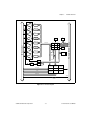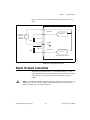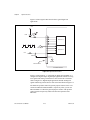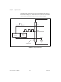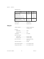
1
DAQ
6711/6713/6715 User
Manual
Analog Voltage Output Device for
PCI/PXI/CompactPCI/PCMCIA/1394 Bus Computers
6711/6713/6715 User Manual
December 1999 Edition
Part Number 322080B-01
Worldwide Technical Support and Product Information
www.ni.com
National Instruments Corporate Headquarters
11500 North Mopac Expressway
Austin, Texas 78759-3504
USA Tel: 512 794 0100
Worldwide Offices
Australia 03 9879 5166, Austria 0662 45 79 90 0, Belgium 02 757 00 20, Brazil 011 284 5011,
Canada (Calgary) 403 274 9391, Canada (Ontario) 905 785 0085, Canada (Québec) 514 694 8521,
China 0755 3904939, Denmark 45 76 26 00, Finland 09 725 725 11, France 01 48 14 24 24,
Germany 089 741 31 30, Greece 30 1 42 96 427, Hong Kong 2645 3186, India 91805275406,
Israel 03 6120092, Italy 02 413091, Japan 03 5472 2970, Korea 02 596 7456, Mexico (D.F.) 5 280 7625,
Mexico (Monterrey) 8 357 7695, Netherlands 0348 433466, Norway 32 27 73 00, Poland 48 22 528 94 06,
Portugal 351 1 726 9011, Singapore 2265886, Spain 91 640 0085, Sweden 08 587 895 00,
Switzerland 056 200 51 51, Taiwan 02 2377 1200, United Kingdom 01635 523545
For further support information, see the Technical Support Resources appendix. To comment on the
documentation, send e-mail to [email protected]
© Copyright 1998, 1999 National Instruments Corporation. All rights reserved.
Important Information
Warranty
The PCI-6711, PCI-6713, PXI-6711, PXI-6713, DAQPad-6713, and DAQCard-6715 devices are warranted against defects in
materials and workmanship for a period of one year from the date of shipment, as evidenced by receipts or other documentation.
National Instruments will, at its option, repair or replace equipment that proves to be defective during the warranty period. This
warranty includes parts and labor.
The media on which you receive National Instruments software are warranted not to fail to execute programming instructions,
due to defects in materials and workmanship, for a period of 90 days from date of shipment, as evidenced by receipts or other
documentation. National Instruments will, at its option, repair or replace software media that do not execute programming
instructions if National Instruments receives notice of such defects during the warranty period. National Instruments does not
warrant that the operation of the software shall be uninterrupted or error free.
A Return Material Authorization (RMA) number must be obtained from the factory and clearly marked on the outside of
the package before any equipment will be accepted for warranty work. National Instruments will pay the shipping costs of
returning to the owner parts which are covered by warranty.
National Instruments believes that the information in this document is accurate. The document has been carefully reviewed
for technical accuracy. In the event that technical or typographical errors exist, National Instruments reserves the right to
make changes to subsequent editions of this document without prior notice to holders of this edition. The reader should consult
National Instruments if errors are suspected. In no event shall National Instruments be liable for any damages arising out of
or related to this document or the information contained in it.
EXCEPT AS SPECIFIED HEREIN, NATIONAL INSTRUMENTS MAKES NO WARRANTIES, EXPRESS OR IMPLIED, AND SPECIFICALLY DISCLAIMS ANY
WARRANTY OF MERCHANTABILITY OR FITNESS FOR A PARTICULAR PURPOSE. CUSTOMER’S RIGHT TO RECOVER DAMAGES CAUSED BY FAULT OR
NEGLIGENCE ON THE PART OF NATIONAL INSTRUMENTS SHALL BE LIMITED TO THE AMOUNT THERETOFORE PAID BY THE CUSTOMER. NATIONAL
INSTRUMENTS WILL NOT BE LIABLE FOR DAMAGES RESULTING FROM LOSS OF DATA, PROFITS, USE OF PRODUCTS, OR INCIDENTAL OR
CONSEQUENTIAL DAMAGES, EVEN IF ADVISED OF THE POSSIBILITY THEREOF. This limitation of the liability of National Instruments will
apply regardless of the form of action, whether in contract or tort, including negligence. Any action against National Instruments
must be brought within one year after the cause of action accrues. National Instruments shall not be liable for any delay in
performance due to causes beyond its reasonable control. The warranty provided herein does not cover damages, defects,
malfunctions, or service failures caused by owner’s failure to follow the National Instruments installation, operation, or
maintenance instructions; owner’s modification of the product; owner’s abuse, misuse, or negligent acts; and power failure or
surges, fire, flood, accident, actions of third parties, or other events outside reasonable control.
Copyright
Under the copyright laws, this publication may not be reproduced or transmitted in any form, electronic or mechanical, including
photocopying, recording, storing in an information retrieval system, or translating, in whole or in part, without the prior written
consent of National Instruments Corporation.
Trademarks
ComponentWorks™, CVI™, DAQCard™, DAQPad™, DAQ-STC™, LabVIEW™, MITE™, National Instruments™, ni.com™,
NI-DAQ™, NI-PGIA™, PXI™, RTSI™, SCXI™, and VirtualBench™ are trademarks of National Instruments Corporation.
Product and company names mentioned herein are trademarks or trade names of their respective companies.
WARNING REGARDING USE OF NATIONAL INSTRUMENTS PRODUCTS
(1) NATIONAL INSTRUMENTS PRODUCTS ARE NOT DESIGNED WITH COMPONENTS AND TESTING FOR A LEVEL
OF RELIABILITY SUITABLE FOR USE IN OR IN CONNECTION WITH SURGICAL IMPLANTS OR AS CRITICAL
COMPONENTS IN ANY LIFE SUPPORT SYSTEMS WHOSE FAILURE TO PERFORM CAN REASONABLY BE
EXPECTED TO CAUSE SIGNIFICANT INJURY TO A HUMAN.
(2) IN ANY APPLICATION, INCLUDING THE ABOVE, RELIABILITY OF OPERATION OF THE SOFTWARE PRODUCTS
CAN BE IMPAIRED BY ADVERSE FACTORS, INCLUDING BUT NOT LIMITED TO FLUCTUATIONS IN ELECTRICAL
POWER SUPPLY, COMPUTER HARDWARE MALFUNCTIONS, COMPUTER OPERATING SYSTEM SOFTWARE
FITNESS, FITNESS OF COMPILERS AND DEVELOPMENT SOFTWARE USED TO DEVELOP AN APPLICATION,
INSTALLATION ERRORS, SOFTWARE AND HARDWARE COMPATIBILITY PROBLEMS, MALFUNCTIONS OR
FAILURES OF ELECTRONIC MONITORING OR CONTROL DEVICES, TRANSIENT FAILURES OF ELECTRONIC
SYSTEMS (HARDWARE AND/OR SOFTWARE), UNANTICIPATED USES OR MISUSES, OR ERRORS ON THE PART OF
THE USER OR APPLICATIONS DESIGNER (ADVERSE FACTORS SUCH AS THESE ARE HEREAFTER
COLLECTIVELY TERMED “SYSTEM FAILURES”). ANY APPLICATION WHERE A SYSTEM FAILURE WOULD
CREATE A RISK OF HARM TO PROPERTY OR PERSONS (INCLUDING THE RISK OF BODILY INJURY AND DEATH)
SHOULD NOT BE RELIANT SOLELY UPON ONE FORM OF ELECTRONIC SYSTEM DUE TO THE RISK OF SYSTEM
FAILURE. TO AVOID DAMAGE, INJURY, OR DEATH, THE USER OR APPLICATION DESIGNER MUST TAKE
REASONABLY PRUDENT STEPS TO PROTECT AGAINST SYSTEM FAILURES, INCLUDING BUT NOT LIMITED TO
BACK-UP OR SHUT DOWN MECHANISMS. BECAUSE EACH END-USER SYSTEM IS CUSTOMIZED AND DIFFERS
FROM NATIONAL INSTRUMENTS' TESTING PLATFORMS AND BECAUSE A USER OR APPLICATION DESIGNER
MAY USE NATIONAL INSTRUMENTS PRODUCTS IN COMBINATION WITH OTHER PRODUCTS IN A MANNER NOT
EVALUATED OR CONTEMPLATED BY NATIONAL INSTRUMENTS, THE USER OR APPLICATION DESIGNER IS
ULTIMATELY RESPONSIBLE FOR VERIFYING AND VALIDATING THE SUITABILITY OF NATIONAL
INSTRUMENTS PRODUCTS WHENEVER NATIONAL INSTRUMENTS PRODUCTS ARE INCORPORATED IN A
SYSTEM OR APPLICATION, INCLUDING, WITHOUT LIMITATION, THE APPROPRIATE DESIGN, PROCESS AND
SAFETY LEVEL OF SUCH SYSTEM OR APPLICATION.
Contents
About This Manual
Conventions Used in This Manual.................................................................................ix
National Instruments Documentation ............................................................................x
Related Documentation..................................................................................................xi
Chapter 1
Introduction
About the 671X Devices ................................................................................................1-1
Using PXI with CompactPCI.........................................................................................1-2
What You Need to Get Started ......................................................................................1-3
Unpacking ......................................................................................................................1-4
Software Programming Choices ....................................................................................1-4
National Instruments Application Software ....................................................1-4
NI-DAQ Driver Software ................................................................................1-5
Register-Level Programming ..........................................................................1-6
Optional Equipment .......................................................................................................1-7
Custom Cabling .............................................................................................................1-7
Chapter 2
Installation and Configuration
Software Installation ......................................................................................................2-1
Hardware Installation.....................................................................................................2-1
Device Configuration.....................................................................................................2-4
Chapter 3
Hardware Overview
Analog Output................................................................................................................3-4
Analog Output Reference Selection ................................................................3-4
Analog Output Reglitch Selection...................................................................3-4
Digital I/O ......................................................................................................................3-4
Timing Signal Routing...................................................................................................3-5
Programmable Function Inputs .......................................................................3-6
Device and RTSI Clocks .................................................................................3-6
RTSI Triggers..................................................................................................3-7
© National Instruments Corporation
v
6711/6713/6715 User Manual
Contents
Chapter 4
Signal Connections
I/O Connector ................................................................................................................ 4-1
I/O Connector Signal Descriptions ................................................................. 4-4
Analog Output Signal Connections ............................................................................... 4-7
Digital I/O Signal Connections ..................................................................................... 4-9
Power Connections........................................................................................................ 4-11
Timing Connections ...................................................................................................... 4-11
Programmable Function Input Connections ................................................... 4-13
EXTSTROBE* Signal ...................................................................... 4-13
Waveform Generation Timing Connections ................................................... 4-14
WFTRIG Signal................................................................................ 4-14
UPDATE* Signal ............................................................................. 4-15
UISOURCE Signal ........................................................................... 4-16
General-Purpose Timing Signal Connections................................................. 4-17
GPCTR0_SOURCE Signal .............................................................. 4-17
GPCTR0_GATE Signal ................................................................... 4-18
GPCTR0_OUT Signal ...................................................................... 4-18
GPCTR0_UP_DOWN Signal........................................................... 4-19
GPCTR1_SOURCE Signal .............................................................. 4-19
GPCTR1_GATE Signal ................................................................... 4-20
GPCTR1_OUT Signal ...................................................................... 4-21
GPCTR1_UP_DOWN Signal........................................................... 4-22
FREQ_OUT Signal........................................................................... 4-23
Field Wiring Considerations.......................................................................................... 4-23
Chapter 5
Calibration
Loading Calibration Constants ...................................................................................... 5-1
Self-Calibration ............................................................................................................. 5-2
External Calibration....................................................................................................... 5-2
Other Considerations ..................................................................................................... 5-3
Appendix A
Specifications
Appendix B
Common Questions
6711/6713/6715 User Manual
vi
www.ni.com
Contents
Appendix C
Technical Support Resources
Glossary
Index
Figures
Figure 1-1.
The Relationship Between the Programming Environment,
NI-DAQ, and Your Hardware ...............................................................1-6
Figure 3-1.
Figure 3-2.
Figure 3-3.
Figure 3-4.
6711/6713 Block Diagram ....................................................................3-2
6715 Block Diagram .............................................................................3-3
UPDATE* Signal Routing ....................................................................3-5
RTSI Bus Signal Connection ................................................................3-7
Figure 4-1.
Figure 4-2.
68-Pin I/O Connector Pin Assignment for the 671X Device.................4-2
50-Pin I/O Connector Pin Assignment for the 671X Device
When Using the SH68-50 Cable ...........................................................4-3
Analog Output Connections ..................................................................4-9
Digital I/O Connections.........................................................................4-10
Timing I/O Connections........................................................................4-12
WFTRIG Input Signal Timing ..............................................................4-14
WFTRIG Output Signal Timing............................................................4-15
UPDATE* Input Signal Timing............................................................4-15
UPDATE* Output Signal Timing .........................................................4-16
UISOURCE Signal Timing ...................................................................4-16
GPCTR0_SOURCE Signal Timing ......................................................4-17
GPCTR0_GATE Signal Timing in Edge-Detection Mode...................4-18
GPCTR0_OUT Signal Timing..............................................................4-19
GPCTR1_SOURCE Signal Timing ......................................................4-20
GPCTR1_GATE Signal Timing in Edge-Detection Mode...................4-21
GPCTR1_OUT Signal Timing..............................................................4-21
GPCTR Timing Summary.....................................................................4-22
Figure 4-3.
Figure 4-4.
Figure 4-5.
Figure 4-6.
Figure 4-7.
Figure 4-8.
Figure 4-9.
Figure 4-10.
Figure 4-11.
Figure 4-12.
Figure 4-13.
Figure 4-14.
Figure 4-15.
Figure 4-16.
Figure 4-17.
Tables
Table 1-1.
PXI-6711/6713 J2 Pin Assignment .......................................................1-3
Table 4-1.
Table 4-2.
Signal Descriptions for I/O Connector Pins ..........................................4-4
I/O Signal Summary for the 6711/6713 Device....................................4-6
© National Instruments Corporation
vii
6711/6713/6715 User Manual
About This Manual
This manual describes the electrical and mechanical aspects of the
PCI/PXI-6711/6713, DAQPad-6713, and DAQCard-6715 devices and
contains information concerning their operation and programming.
The 6711/6713/6715 devices include:
•
PXI-6711with four or PXI-6713 with eight analog output (AO)
channels, two counters, and eight digital input/output (DIO) channels
for PXI/CompactPCI
•
PCI-6711 with four or PCI-6713 with eight AO channels, two
counters, and eight DIO channels for PCI
•
DAQPad-6713 with eight AO channels, two counters, and eight DIO
channels for IEEE-1394 (Firewire)
•
DAQCard-6715 with eight AO channels, two counters, and eight DIO
channels for PCMCIA (PC Card)
Your PCI/PXI-6711/6713, DAQPad-6713, and DAQCard-6715 device is a
multifunction analog output, DIO, and timing input/output (I/O) device for
PCI/PXI/CompactPCI, 1394, and PCMCIA (PC Card) buses.
Conventions Used in This Manual
The following conventions are used in this manual.
<>
Angle brackets enclose the name of a key on the keyboard (for example,
<option>). Angle brackets containing numbers separated by an ellipsis
represent a range of values associated with a bit or signal name
(for example, DIO<3..0>).
♦
The ♦ indicates that the text following it applies to only to a specific
PCI/PXI/CompactPCI, DAQCard, and 1394 device.
This icon denotes a note, which alerts you to important information.
This icon denotes a caution, which advises you of precautions to take to
avoid injury, data loss, or a system crash.
italic
Italic text denotes emphasis, a cross reference, or an introduction to a key
concept. This font also denotes text from which you supply the appropriate
word or value, as in NI-DAQ 6.X.
© National Instruments Corporation
ix
6711/6713/6715 User Manual
About This Manual
671X
671X refers to the National Instruments PCI/PXI-6711/6713,
DAQPad-6713, and DAQCard-6715 devices unless otherwise noted.
NI-DAQ
NI-DAQ refers to the NI-DAQ driver software for PC compatible
computers unless otherwise noted.
PC
Refers to all PC AT series computers with PCI bus unless otherwise noted.
SCXI
SCXI stands for Signal Conditioning eXentsions for Instrumentation and is
a National Instruments product line designed to perform front-end signal
conditioning for National instruments plug-in DAQ devices.
National Instruments Documentation
The 671X User Manual is one piece of the documentation set for your DAQ
system. You could have any of several types of documentation depending
on the hardware and software in your system. Use the documentation you
have as follows:
6711/6713/6715 User Manual
•
Getting Started with SCXI—If you are using SCXI, this is the first
manual you should read. It gives an overview of the SCXI system and
contains the most commonly needed information for the modules,
chassis, and software.
•
Your SCXI hardware user manuals—If you are using SCXI, read these
manuals next for detailed information about signal connections and
module configuration. They also explain in greater detail how the
module works and contain application hints.
•
Your DAQ hardware documentation—This documentation has
detailed information about the DAQ hardware that plugs into or is
connected to your computer. Use this documentation for hardware
installation and configuration instructions, specification information
about your DAQ hardware, and application hints.
•
Software documentation—You may have both application software
and NI-DAQ software documentation. National Instruments
application software includes ComponentWorks, LabVIEW,
LabWindows/CVI, and VirtualBench. After you set up your hardware
system, use either your application software documentation or the
NI-DAQ documentation to help you write your application. If you have
a large, complicated system, it is worthwhile to look through the
software documentation before you configure your hardware.
x
www.ni.com
About This Manual
•
Accessory installation guides or manuals—If you are using accessory
products, read the terminal block and cable assembly installation
guides. They explain how to physically connect the relevant pieces of
the system. Consult these guides when you are making your
connections.
•
SCXI chassis manuals—If you are using SCXI, read these manuals for
maintenance information on the chassis and installation instructions.
Related Documentation
The following documents contain information you may find helpful:
•
DAQ-STC Technical Reference Manual
•
National Instruments Application Note 025, Field Wiring and Noise
Considerations for Analog Signals
•
PCI Local Bus Specification Revision 2.0
•
IEEE 1394-1995 specification
© National Instruments Corporation
xi
6711/6713/6715 User Manual
1
Introduction
This chapter describes your 671X device, lists what you need to get started,
describes the optional software and optional equipment, and explains how
to unpack your 671X device.
About the 671X Devices
Thank you for buying a National Instruments 671X device. Your 671X
device is a completely Plug and Play, analog output, digital, and timing I/O
device for PXI/PCI/CompactPCI, 1394, or PCMCIA (PC Card) bus. The
671X device features a 12-bit digital-to-analog converter (DAC) per
channel with update rates up to 1 MS/s/channel for voltage outputs, eight
lines of TTL-compatible digital I/O, and two 24-bit counter/timers for
timing I/O. The 6711 device features four voltage output channels, while
the 6713 and 6715 devices feature eight voltage output channels. Because
the 671X device has no DIP switches, jumpers, or potentiometers, it is
easily software-configured and calibrated.
The 6711/6713 device is a completely switchless and jumperless data
acquisition (DAQ) device for the PXI/PCI/CompactPCI or 1394 bus. This
feature is made possible by the National Instruments MITE bus interface
chip that connects the device to the PCI I/O bus. The MITE implements the
PCI Local Bus Specification so that the interrupts and base memory
addresses are all software configured.
The 6715 device is a completely switchless and jumperless data acquisition
(DAQ) device for the PCMCIA (PC Card) bus and is Plug and Play
software configurable.
The 671X device uses the National Instruments DAQ-STC system timing
controller for time-related functions. The DAQ-STC consists of three
timing groups that control analog input, analog output, and general-purpose
counter/timer functions. These groups include a total of seven 24-bit and
three 16-bit counters and a maximum timing resolution of 50 ns. The
analog input section of the DAQ-STC is unused by the 671X.
© National Instruments Corporation
1-1
6711/6713/6715 User Manual
Chapter 1
Introduction
♦
PCI/PXI/Compact PCI-6711/6713 only
Often with other DAQ devices, you cannot easily synchronize several
measurement functions to a common trigger or timing event. The
PXI/CompactPCI-6711/6713 device has the Real-Time System Integration
(RTSI) bus to solve this problem. The RTSI bus consists of our RTSI bus
interface and a ribbon cable to route timing and trigger signals between
several functions on as many as five DAQ devices in your computer. If you
are using the PXI-6711/6713 in a PXI chassis, RTSI lines, known as the
PXI trigger bus, are part of the backplane, therefore you do not need the
RTSI cable for system triggering and timing on the PXI.
♦
DAQCard-6715 only
The DAQCard-6715 provides access to timing and triggering signals
through the I/O connector for synchronization to other DAQ devices or
timing signals.
Detailed specifications of the 671X device are in Appendix A,
Specifications.
Using PXI with CompactPCI
♦
PXI/CompactPCI-6711/6713 Only
Using PXI-compatible products with standard CompactPCI products is an
important feature provided by the PXI Specification, revision 1.0. If you use
a PXI-compatible plug-in device in a standard CompactPCI chassis, you
cannot use PXI-specific functions, but you can still use the basic plug-in
device functions. For example, the PXI trigger bus on your 6711/6713
device is available in a PXI chassis but not in a CompactPCI chassis.
The CompactPCI specification permits vendors to develop sub-buses that
coexist with the basic PCI interface on the CompactPCI bus. Compatible
operation is not guaranteed between CompactPCI devices with different
sub-buses nor between CompactPCI devices with sub-buses and PXI.
The standard implementation for CompactPCI does not include these
sub-buses. Your 6711/6713 device will work in any standard CompactPCI
chassis adhering to the PICMG CompactPCI 2.0 R2.1 document.
PXI-specific features, RTSI bus trigger, RTSI Clock, and Serial
Communication, are implemented on the J2 connector of the CompactPCI
bus. Table 1-1 lists the J2 pins used by your PXI/CompactPCI-6711/6713,
6711/6713/6715 User Manual
1-2
www.ni.com
Chapter 1
Introduction
which is compatible with any CompactPCI chassis with a sub-bus that does
not drive these lines. Even if the sub-bus is capable of driving these lines,
the 6711/6713 is still compatible as long as those pins on the sub-bus are
disabled by default and are never enabled. Damage can result if these lines
are driven by the sub-bus.
Table 1-1. PXI-6711/6713 J2 Pin Assignment
6711/6713 Signal
PXI Pin Name
PXI J2 Pin Number
RTSI Trigger <0..5>
PXI Trigger <0..5>
B16, A16, A17,
A18, B18, C18
RTSI Trigger 6
PXI Star Trigger
D17
RTSI Clock
PXI Trigger (7)
E16
Serial
Communication
LBR (6, 7, 8, 9, 10,
11, 12)
EI5, A3, C3, D3, E3,
A2, B2
What You Need to Get Started
To set up and use the 671X device, you will need the following:
❑ Either the 6711, 6713, or 6715 device
❑ 6711/6713/6715 User Manual
❑ NI-DAQ driver for PC compatibles version 6.5 or higher (6.7 or higher
for DAQCard-6715)
❑ One of the following software packages and documentation:
–
LabVIEW for Windows
–
LabWindows/CVI for Windows
–
ComponentWorks
–
VirtualBench
–
C language compiler
❑ Your computer
❑ SH68-68 EP cable (PCI/PXI/CompactPCI-6711/13 and
DAQPad-6713)
© National Instruments Corporation
1-3
6711/6713/6715 User Manual
Chapter 1
Introduction
❑ SHC68-68EP cable (DAQCard-6715)
❑ One of the following:
–
BNC 2110 signal connector block
–
SCB-68 shielded terminal block
–
CB-68LP terminal block
Unpacking
The 671X device is shipped in an antistatic package to prevent electrostatic
damage to the device. Electrostatic discharge can damage several
components on the device. To avoid such damage in handling the device,
take the following precautions:
•
Ground yourself using a grounding strap or by holding a grounded
object.
•
Touch the antistatic package to a metal part of your computer chassis
before removing the device from the package.
•
Remove the device from the package and inspect the device for
loose components or any other sign of damage. Notify National
Instruments if the device appears damaged in any way. Do not install
a damaged device into your computer.
•
Never touch the exposed pins of connectors.
Software Programming Choices
You have several options to choose from when programming your National
Instruments DAQ and SCXI hardware. You can use National Instruments
application software, NI-DAQ, or register-level programming.
National Instruments Application Software
LabVIEW features interactive graphics, a state-of-the-art user interface,
and a powerful graphical programming language. The LabVIEW Data
Acquisition VI Library, a series of VIs for using LabVIEW with National
Instruments DAQ hardware, is included with LabVIEW. The LabVIEW
Data Acquisition VI Library is functionally equivalent to NI-DAQ
software.
6711/6713/6715 User Manual
1-4
www.ni.com
Chapter 1
Introduction
LabWindows/CVI features interactive graphics, state-of-the-art user
interface, and uses the ANSI standard C programming language. The
LabWindows/CVI Data Acquisition Library, a series of functions for using
LabWindows/CVI with National Instruments DAQ hardware, is included
with the NI-DAQ software kit. The LabWindows/CVI Data Acquisition
Library is functionally equivalent to the NI-DAQ software.
ComponentWorks contains tools for data acquisition and instrument
control built on NI-DAQ driver software. ComponentWorks provides
a higher-level programming interface for building virtual instruments
through standard OLE controls and DLLs. With ComponentWorks, you
can use all of the configuration tools, resource management utilities, and
interactive control utilities included with NI-DAQ.
VirtualBench features virtual instruments that combine DAQ products,
software, and your computer to create a stand-alone instrument with the
added benefit of the processing, display, and storage capabilities of your
computer. VirtualBench instruments load and save waveform data to disk
in the same forms that used in popular spreadsheet programs and word
processors.
Using ComponentWorks, LabVIEW, LabWindows/CVI, or VirtualBench
software will greatly reduce the development time for your data acquisition
and control application.
NI-DAQ Driver Software
The NI-DAQ driver software is included at no charge with all National
Instruments DAQ hardware. NI-DAQ is not packaged with SCXI or
accessory products, except for the SCXI-1200. NI-DAQ has an extensive
library of functions that you can call from your application programming
environment. These functions include routines for analog input (A/D
conversion), buffered data acquisition (high-speed A/D conversion),
analog output (D/A conversion), waveform generation (timed D/A
conversion), digital I/O, counter/timer operations, SCXI, RTSI,
self-calibration, messaging, and acquiring data to extended memory.
NI-DAQ has both high-level DAQ I/O functions for maximum ease of use
and low-level DAQ I/O functions for maximum flexibility and
performance. Examples of high-level functions are streaming data to disk
or acquiring a certain number of data points. An example of a low-level
function is writing directly to registers on the DAQ device. NI-DAQ does
not sacrifice the performance of National Instruments DAQ devices
because it lets multiple devices operate at their peak.
© National Instruments Corporation
1-5
6711/6713/6715 User Manual
Chapter 1
Introduction
NI-DAQ also internally addresses many of the complex issues between the
computer and the DAQ hardware such as programming interrupts and
DMA controllers. NI-DAQ maintains a consistent software interface
among its different versions so that you can change platforms with minimal
modifications to your code. Whether you are using conventional
programming languages or National Instruments application software, your
application uses the NI-DAQ driver software, as illustrated in Figure 1-1.
Conventional
Programming
Environment
ComponentWorks,
LabVIEW,
LabWindows/CVI,
or VirtualBench
NI-DAQ
Driver Software
DAQ or
SCXI Hardware
Personal Computer
or Workstation
Figure 1-1. The Relationship Between the Programming Environment,
NI-DAQ, and Your Hardware
Register-Level Programming
The final option for programming any National Instruments DAQ
hardware is to write register-level software. Writing register-level
programming software can be very time-consuming and inefficient, and is
not recommended for most users.
Even if you are an experienced register-level programmer, using NI-DAQ
or application software to program your National Instruments DAQ
hardware is easier than, and as flexible as, register-level programming, and
can save weeks of development time.
6711/6713/6715 User Manual
1-6
www.ni.com
Chapter 1
Introduction
Optional Equipment
National Instruments offers a variety of products to use with the 671X
device, including cables, connector blocks, and other accessories, as
follows:
•
Cables and cable assemblies
•
Connector blocks, shielded and unshielded 50- and 68-pin screw
terminals
•
RTSI bus cables
•
Low channel-count digital signal conditioning modules, devices, and
accessories
For more specific information about these products, refer to your National
Instruments catalogue or call the office nearest you.
Custom Cabling
National Instruments offers cables and accessories for you to prototype
your application or to use if you frequently change device interconnections.
If you want to develop your own cable, however, the following guidelines
can be useful:
•
Route the analog lines separately from the digital lines.
•
When using a cable shield, use separate shields for the analog and
digital halves of the cable. Failure to do so results in noise coupling
into the analog signals from transient digital signals.
Mating connectors and a backshell kit for making custom 68-pin cables are
available from National Instruments.
The following list gives recommended connectors that mate to the I/O
connector on the 6711/6713 device:
•
Honda 68-position, solder cup, female connector
•
Honda backshell
The following list gives recommended connectors that mate to the I/O
connector on the 6715 device:
•
Amp 68-position, VHDCI
•
Amp backshell
© National Instruments Corporation
1-7
6711/6713/6715 User Manual
Installation and Configuration
2
This chapter explains how to install and configure your 671X device.
Software Installation
Install your software before you install the 671X device. Refer to the
appropriate release notes indicated below for specific instructions on the
software installation sequence.
1.
Install your application software—If you are using LabVIEW,
LabWindows/CVI, or other National Instruments application software
packages, refer to the appropriate release notes.
2.
Install the NI-DAQ driver software—Refer to your NI-DAQ release
notes and follow the instructions given there for your operating system
and application software package.
You can now install your hardware.
Hardware Installation
You can install the PCI/PXI-6711/6713 device in any available PXI/PCI
expansion slot in your computer. You can connect the DAQPad-6713 to
any available 1394 port on your PC or another 1394 device. You can install
the DAQCard-6715 in any available 5 V PC Card slot in your computer.
However, to achieve best noise performance, leave as much room as
possible between the 671X device and other devices and hardware. The
following are general installation instructions, but consult your computer
user manual or technical reference manual for specific instructions and
warnings.
♦
PXI-6711/6713
You can install the PXI-6711/6713 in any available PXI slot in your PXI or
CompactPCI chassis.
© National Instruments Corporation
2-1
6711/6713/6715 User Manual
Chapter 2
Installation and Configuration
Note The PXI-6711/6713 has connections to several reserved lines on the CompactPCI J2
connector. Before installing the PXI-6711/6713 in a CompactPCI system that uses J2
connector lines for a purpose other than PXI, see Using PXI with CompactPCI in
Chapter 1, Introduction.
1.
Turn off and unplug your PXI or CompactPCI chassis.
2.
Choose an unused PXI or CompactPCI peripheral slot. For maximum
performance, install the PXI-6711/6713 in a slot that supports bus
arbitration or bus-master cards. The PXI-6711/6713 contains onboard
bus-master DMA logic that can operate only in such a slot. If you
choose a slot that does not support bus masters, you will have to disable
the onboard DMA controller using your software. PXI-compliant
chassis must have bus arbitration for all slots.
3.
Remove the filter panel for the peripheral slot that you have chosen.
4.
Touch a metal part on the chassis to discharge any static electricity that
might be on your clothes or body.
5.
Insert the PXI-6711/6713 device in the 5 V slot. Use the
injector/ejector handle to fully inject the device into place.
6.
Screw the front panel of the PXI-6711/6713 to the front panel
mounting rails of the PXI or CompactPCI chassis.
7.
Visually verify the installation.
8.
Plug in and turn on the PXI or CompactPCI chassis.
The PXI-6711/6713 is now installed.
♦
6711/6713/6715 User Manual
PCI-6711/6713
1.
Turn off and unplug your computer.
2.
Remove the top cover or access port to the I/O channel.
3.
Remove the expansion slot cover on the back panel of the computer.
4.
Insert the 6711/6713 device into a 5 V PCI slot. Gently rock the device
to ease it into place. It can be a tight fit, but do not force the device into
place.
5.
If required, screw the mounting bracket of the 6711/6713 device to the
back panel rail of the computer.
6.
Replace the cover.
7.
Plug in and turn on your computer.
2-2
www.ni.com
Chapter 2
Installation and Configuration
The PCI-6711/6713 device is installed. You are now ready to configure
your software. Refer to your software documentation for configuration
instructions.
♦
♦
DAQPad-6713
1.
Connect the 1394 cable from the computer or any other 1394 device to
the port on your DAQPad device.
2.
Connect the power cord to the wall outlet and the DAQPad device.
3.
Flip the rocker switch to turn on the power for the DAQPad-6713. Your
computer should detect your DAQPad device immediately and when
the computer recognizes your DAQPad device, the COM LED on the
front panel will blink once. The power LED should be on.
4.
Configure your DAQPad device and any accessories with the
Measurement & Automation Explorer.
DAQCard-6715
1.
Insert the DAQCard and attach the I/O cable. The DAQCard has two
connectors—a 68-pin PCMCIA bus connector on one end and a 68-pin
I/O connector on the other end. Insert the PCMCIA bus connector into
any available Type II PCMCIA slot until the connector is seated firmly.
The DAQCard and I/O cable are both keyed so that you can attach the
cable only one way.
Note Be careful not to put strain on the I/O cable when inserting it into and removing it
from the DAQCard. Always grasp the cable by the connector you are plugging or
unplugging. Never pull directly on the I/O cable to unplug it from the DAQCard.
You can connect your DAQCard to 68- and 50-pin accessories. You can use either a 68-pin
female cable to plug into the PSHR68-68M with your DAQCard, or a 50-pin male cable
and the PSHR68-68M and SH6850 with your DAQCard.
2.
Tighten the jackscrews to secure the cable to the DAQCard.
3.
Configure your DAQPad device and any accessories with
Measurement & Automation Explorer.
© National Instruments Corporation
2-3
6711/6713/6715 User Manual
Chapter 2
Installation and Configuration
Device Configuration
Due to the National Instruments standard architecture for data acquisition,
the PCI bus specification, the IEEE-1394-1995 specification, the PCMCIA
(PC Card) specification, and the 671X device is completely software
configurable. There are two types of configuration on the 671X
device—bus-related and data acquisition-related configuration.
The PCI/PXI-6711/6713 device is fully compatible with the
industry-standard PCI Local Bus Specification Revision 2.0. This
specification allows the PCI system to automatically perform all
bus-related configurations and requires no user interaction. Bus-related
configuration includes setting the device base memory address and
interrupt channel.
Data acquisition-related configuration includes such settings as analog
output range, reference selection, and others. You can modify these settings
using NI-DAQ C language API, or application level software, such as
ComponentWorks, LabVIEW, LabWindows/CVI, and VirtualBench.
6711/6713/6715 User Manual
2-4
www.ni.com
3
Hardware Overview
This chapter presents an overview of the hardware functions on your
PCI/PXI-6711/6713 and DAQPad-6713 device. Figure 3-1 shows a block
diagram of the 6711/6713 device. Figure 3-2 shows a block diagram of the
6715 device.
© National Instruments Corporation
3-1
6711/6713/6715 User Manual
Chapter 3
Hardware Overview
CH0
Amp
CH0
12-Bit DAC
12
CH0
Latch
CH1
12-Bit DAC
12
CH2
Amp
CH2
12-Bit DAC
12
CH2
Latch
CH3
Amp
CH3
12-Bit DAC
12
CH3
Latch
CH1
Latch
Data
Data
400
Mbps
1394 PHY
Control
CH1
Amp
IEEE 1394
DAQPad-6713 only
Control
NI
Firephli
Address/Data
CH4
Amp
CH4
12-Bit DAC
12
CH4
Latch
CH5
Amp
CH5
12-Bit DAC
12
CH5
Latch
Control
CH6
12-Bit DAC
12
CH6
Latch
CH7
Amp
CH7
12-Bit DAC
12
CH7
Latch
AO Control
24
8
Calibration
Mux
Address/Data
EEPROM
EEPROM
Control
Register
Decode
AO
Control
FPGA
DMA/
IRQ
DMA
DAQ-STC
Bus
Interface
Calibration
Control
Calibration
DACs
IRQ
PCI/PXI
CH6
Amp
PCI
PCI
Bus
MITE Interface
Data
DAC
FIFO
Address
I/O Connector
Data
Generic
Bus
Interface
Data
Calibration
ADC
PFI / Trigger
Timing
Digital I/O (8)
Bus
Interface
Trigger
Analog Output
Timing/Control
Counter/
Timing I/O
DAQ - STC
DMA/IRQ
Digital I/O
Analog Input
Timing/Control
RTSI Bus
Interface
+5 V
1A
RTSI Bus
Note: CH4 through CH7 on 6713 only
Figure 3-1. 6711/6713 Block Diagram
6711/6713/6715 User Manual
3-2
www.ni.com
CH0
12-Bit DAC
CH1
Amp
CH1
12-Bit DAC
CH2
Amp
CH2
12-Bit DAC
CH3
Amp
CH3
12-Bit DAC
CH4
Amp
CH4
12-Bit DAC
CH5
Amp
CH5
12-Bit DAC
CH6
Amp
CH6
12-Bit DAC
CIS
EEPROM
CONFIG
EEPROM
Control/Data
DAC
Control
Bus
Interface
Address/Control
AO
Control
Bus
Interface
Data
FIFO
Data In
FPGA
DAQ-STC Calibration
Interface
Control
EEPROM
CH7
12-Bit DAC
24
8
Calibration
Mux
DAC
FIFO
Data/Control
CH7
Amp
Control
Digital
Thermometer
PC-Card (PCMCIA) Bus
CH0
Amp
Hardware Overview
Data
I/O Connector
Chapter 3
Calibration
DACs
Calibration
ADC
PFI / Trigger
Analog Output
Timing/Control
Bus
Interface
Trigger
DAQ-STC
IRQ
Digital I/O
RTSI Bus
Interface
Counter/
Timing I/O
Timing
Analog Input
Timing/Control
Digital I/O (8)
+5 V
0.75 A
Figure 3-2. 6715 Block Diagram
© National Instruments Corporation
3-3
6711/6713/6715 User Manual
Chapter 3
Hardware Overview
Analog Output
The 6711 has four channels and the 6713/6715 has eight channels of
voltage output at the I/O connector. The reference for the analog output
circuitry is software selectable per channel. The reference can be either
internal or external, whereas the range is always bipolar. This means that
you can output signals up to ±10 V with internal reference selected or ±
EXTREF voltage with external reference selected.
Analog Output Reference Selection
You can connect each D/A converter (DAC) to the internal reference of
10 V or to the external reference signal connected to the external reference
(EXTREF) pin on the I/O connector. This signal applied to EXTREF
should be within ±11 V of AOGND. You can configure each channel to use
either internal or external reference. The default reference value selection
is internal reference.
Analog Output Reglitch Selection
In normal operation, a DAC output will glitch whenever it is updated with
a new value. The glitch energy differs from code to code and appears as
distortion in the frequency spectrum. Each analog output channel contains
a reglitch circuit that generates uniform glitch energy at every code rather
than large glitches at the major code transitions. This uniform glitch energy
appears as a multiple of the update rate in the frequency spectrum. Notice
that this reglitch circuit does not eliminate the glitches; it only makes them
more uniform in size. By default, reglitching is disabled for all channels,
however you can use NI-DAQ to independently enable reglitching for each
channel.
Digital I/O
The 671X device contains eight lines of digital I/O for general-purpose use.
You can individually software-configure each line for either input or
output. At system startup and reset, the digital I/O ports are all high
impedance.
The hardware up/down control for general-purpose counters 0 and 1 are
connected onboard to DIO6 and DIO7, respectively. Thus, you can use
DIO6 and DIO7 to control the general-purpose counters. The up/down
control signals are input only and do not affect the operation of the
DIO lines.
6711/6713/6715 User Manual
3-4
www.ni.com
Chapter 3
Hardware Overview
Timing Signal Routing
The DAQ-STC provides a very flexible interface for connecting timing
signals to other devices or external circuitry. The 6711/6713 device uses
the RTSI bus to interconnect timing signals between devices
(PCI/PXI/CompactPCI) and the Programmable Function Input (PFI) pins
on the I/O connector to connect the device to external circuitry. These
connections are designed to enable the 6711/6713 device to both control
and be controlled by other devices and circuits.
There are a total of 13 timing signals internal to the DAQ-STC that you can
control by an external source. You can also control these timing signals
control by signals generated internally to the DAQ-STC, and these
selections are fully software configurable. For example, the signal routing
multiplexer for controlling the UPDATE* signal is shown in Figure 3-3.
RTSI Trigger <0..6>
UPDATE*
PFI<0..9>
Update Interval Counter TC
GPCTR0_OUT
Figure 3-3. UPDATE* Signal Routing
© National Instruments Corporation
3-5
6711/6713/6715 User Manual
Chapter 3
Hardware Overview
Figure 3-3 shows that you can generate UPDATE* from a number of
sources, including the external signals RTSI<0..6> and PFI<0..9> and the
internal signals Sample Interval Counter TC and GPCTR0_OUT.
Many of these timing signals are also available as outputs on the RTSI pins,
as indicated in the RTSI Triggers section later in this chapter, and on the
PFI pins, as indicated in Chapter 4, Signal Connections.
Programmable Function Inputs
♦
6711/6713
The 10 PFIs are connected to the signal routing multiplexer for each timing
signal, and software can select one of the PFIs as the external source for a
given timing signal. It is important to note that you can use any of the PFIs
as an input by any of the timing signals and that multiple timing signals can
use the same PFI simultaneously. This flexible routing scheme reduces the
need to change physical connections to the I/O connector for different
applications. You can also individually enable each of the PFI pins to output
a specific internal timing signal. For example, if you need the UPDATE*
signal as an output on the I/O connector, software can turn on the output
driver for the PFI5/UPDATE* pin.
Device and RTSI Clocks
♦
6711/6713
Many functions performed by the 6711/6713 device require a frequency
timebase to generate the necessary timing signals for controlling DAC
updates or general-purpose signals at the I/O connector.
The 6711/6713 device can use either its internal 20 MHz timebase or a
timebase received over the RTSI bus. In addition, if you configure the
device to use the internal timebase, you can also program the device to drive
its internal timebase over the RTSI bus to another device that is
programmed to receive this timebase signal. This clock source, whether
local or from the RTSI bus, is used directly by the device as the primary
frequency source. The default configuration at startup is to use the internal
timebase without driving the RTSI bus timebase signal. This timebase is
software selectable.
6711/6713/6715 User Manual
3-6
www.ni.com
Chapter 3
Hardware Overview
RTSI Triggers
The seven RTSI trigger lines on the RTSI bus provide a very flexible
interconnection scheme for the 6711/6713 device sharing the RTSI bus.
These bidirectional lines can drive any of five timing signals onto the RTSI
bus and can receive any of these timing signals. This signal connection
scheme is shown in Figure 3-4.
DAQ-STC
WFTRIG
GPCTR0_SOURCE
RTSI Switch
RTSI Bus Connector
UPDATE*
Trigger
7
GPCTR0_GATE
GPCTR0_OUT
UISOURCE
GPCTR1_SOURCE
Clock
GPCTR1_GATE
switch
RTSI_OSC (20 MHz)
Figure 3-4. RTSI Bus Signal Connection
Refer to the Timing Connections section of Chapter 4, Signal Connections,
for a description of the signals.
© National Instruments Corporation
3-7
6711/6713/6715 User Manual
4
Signal Connections
This chapter describes how to make input and output signal connections to
your 671X device through the device I/O connector.
♦
PCI/PXI-6711/6713, DAQCard-6715
The I/O connector for the 6711/6713 device has 68 pins that you can
connect to 68-pin accessories with the SH68-68-EP or similar 68-pin
shielded cable.
♦
DAQPad-6713
The DAQPad-6713 allows connection to all analog and some digital signals
through BNC connectors. You can access the remaining digital signals
using the removable screw terminal block on the front panel.
I/O Connector
Figure 4-1 shows the pin assignments for the 68-pin I/O connector on the
671X device. Figure 4-2 shows the pin assignments for the 50-pin I/O cable
connector when used with the 671X device. A signal description follows
the connector pinouts.
© National Instruments Corporation
4-1
6711/6713/6715 User Manual
Chapter 4
Signal Connections
AOGND
NC
AOGND
AOGND
DAC6OUT1
AOGND
DAC5OUT1
AOGND
AOGND
DAC3OUT
AOGND
AOGND
DAC0OUT
DAC1OUT
EXTREF
DIO4
DGND
DIO1
DIO6
DGND
+5 V
DGND
DGND
PFI0
PFI1
DGND
+5 V
DGND
PFI5/UPDATE*
PFI6/WFTRIG
DGND
PFI9/GPCTR0_GATE
GPCTR0_OUT
FREQ_OUT
1
34
33
32
31
30
29
28
27
26
25
24
23
22
21
20
19
18
17
16
15
14
13
12
11
10
9
8
7
6
5
4
3
2
1
68
67
66
65
64
63
62
61
60
59
58
57
56
55
54
53
52
51
50
49
48
47
46
45
44
43
42
41
40
39
38
37
36
35
NC
AOGND
AOGND
DAC7OUT1
AOGND
AOGND
NC
AOGND
DAC4OUT1
AOGND
AOGND
DAC2OUT
AOGND
AOGND
AOGND
DGND
DIO0
DIO5
DGND
DIO2
DIO7
DIO3
NC
EXTSTROBE*
DGND
PFI2
PFI3/GPCTR1_SOURCE
PFI4/GPCTR1_GATE
GPCTR1_OUT
DGND
PFI7
PFI8/GPCTR0_SOURCE
DGND
DGND
No Connect on PCI/PXI 6711
Figure 4-1. 68-Pin I/O Connector Pin Assignment for the 671X Device
6711/6713/6715 User Manual
4-2
www.ni.com
Chapter 4
AOGND
NC
NC
DAC7OUT1
DAC6OUT1
DAC5OUT1
DAC4OUT1
DAC3OUT
DAC2OUT
NC
DAC1OUT
AOGND
DIO0
DIO1
DIO2
DIO3
DGND
+5 V
EXTSTROBE*
PFI1/TRIG2
PFI3/GPCTR1_SOURCE
GPCTR1_OUT
PFI6/WFTRIG
PFI8/GPCTR0_SOURCE
GPCTR0_OUT
1No
1
3
5
7
9
11
13
15
17
19
21
23
25
27
29
31
33
35
37
39
41
43
45
47
49
2
4
6
8
10
12
14
16
18
20
22
24
26
28
30
32
34
36
38
40
42
44
46
48
50
Signal Connections
AOGND
AOGND
AOGND
AOGND
AOGND
AOGND
AOGND
AOGND
AOGND
DAC0OUT
EXTREF
DGND
DIO4
DIO5
DIO6
DIO7
+5 V
SCANCLK
PFI0/TRIG1
PFI2/CONVERT*
PFI4/GPCTR1_GATE
PFI5/UPDATE*
PFI7/STARTSCAN
PFI9/GPCTR0_GATE
FREQ_OUT
Connect on PCI/PXI-6711
Figure 4-2. 50-Pin I/O Connector Pin Assignment for the 671X Device When Using
the SH68-50 Cable
© National Instruments Corporation
4-3
6711/6713/6715 User Manual
Chapter 4
Signal Connections
Connections that exceed any of the maximum ratings of input or output signals
on the 671X device can damage the 671X device and the computer. Maximum input ratings
for each signal are given in the Protection column of Table 4-2. National Instruments is not
liable for any damages resulting from such signal connections.
Caution
I/O Connector Signal Descriptions
Table 4-1. Signal Descriptions for I/O Connector Pins
Signal Name
AOGND
DAC<0..7>OUT
Reference
Direction
—
—
Analog Output Ground—The analog output voltages are
referenced to this node.
Output
Analog Output Channels 0 through 7—These pins supply
the voltage output of the respective channel.
—
—
Digital Ground—This pin supplies the reference for the
digital signals at the I/O connector as well as the +5 VDC
supply.
DIO<0..7>
DGND
Input or
Output
Digital I/O signals—DIO6 and 7 can control the up/down
signal of general-purpose counters 0 and 1, respectively.
+5 V
DGND
Output
+5 VDC Source—These pins are fused for up to 1 A
(0.75 A, DAQCard-6715)1 of +5 V supply. The fuse is
self-resetting.
EXTREF
AOGND
Input
External Reference—This is the external reference input for
the analog output circuitry.
EXTSTROBE*
DGND
Output
External Strobe—This output is used for controlling SCXI
devices.
PFI0
DGND
Input
PFI0—As an input, this is one of the Programmable
Function Inputs (PFIs). PFI signals are explained in the
Timing Connections section later in this chapter. PFI0
cannot be an output.
PFI1
DGND
Input
PFI1—As an input, this is one of the PFIs. PFI1 cannot be
an output.
PFI2
DGND
Input
PFI2—As an input, this is one of the PFIs. PFI2 cannot be
an output.
PFI3/GPCTR1_SOURCE
DGND
Input
PFI3/Counter 1 Source—As an input, this is one of the
PFIs.
Output
As an output, this is the GPCTR1_SOURCE signal. This
signal reflects the actual source connected to the
general-purpose counter 1.
DGND
6711/6713/6715 User Manual
AOGND
Description
4-4
www.ni.com
Chapter 4
Signal Connections
Table 4-1. Signal Descriptions for I/O Connector Pins (Continued)
Signal Name
PFI4/GPCTR1_GATE
Reference
DGND
Direction
Description
Input
PFI4/Counter 1 Gate—As an input, this is one of the PFIs.
Output
As an output, this is the GPCTR1_GATE signal. This signal
reflects the actual gate signal connected to the
general-purpose counter 1.
GPCTR1_OUT
DGND
Output
Counter 1 Output—This output is from the general-purpose
counter 1 output.
PFI5/UPDATE*
DGND
Input
PFI5/Update—As an input, this is one of the PFIs.
Output
As an output, this is the UPDATE* signal. A high-to-low
edge on UPDATE* indicates that the analog output
waveform generation group is being updated.
Input
PFI6/Waveform Trigger—As an input, this is one of the
PFIs.
Output
As an output, this is the WFTRIG signal. In timed analog
output sequences, a low-to-high transition indicates the
initiation of the waveform generation.
PFI6/WFTRIG
DGND
PFI7
DGND
Input
PFI7—As an input, this is one of the PFIs. PFI7 cannot be
an output.
PFI8/GPCTR0_SOURCE
DGND
Input
PFI8/Counter 0 Source—As an input, this is one of the
PFIs.
Output
As an output, this is the GPCTR0_SOURCE signal. This
signal reflects the actual source connected to the
general-purpose counter 0.
Input
PFI9/Counter 0 Gate—As an input, this is one of the PFIs.
Output
As an output, this is the GPCTR0_GATE signal. This signal
reflects the actual gate signal connected to the
general-purpose counter 0.
PFI9/GPCTR0_GATE
DGND
GPCTR0_OUT
DGND
Output
Counter 0 Output—This output is from the general-purpose
counter 0 output.
FREQ_OUT
DGND
Output
Frequency Output—This output is from the frequency
generator output.
1 The +5 V line on the connector of the DAQCard-6715 is fused at 0.75 A, however, the actual current available can be limited
below this value by the host computer. National Instruments recommends limiting current from this line to 250 mA.
© National Instruments Corporation
4-5
6711/6713/6715 User Manual
Chapter 4
Signal Connections
Table 4-2 shows the I/O signal summary for the 6711/6713 devices.
Table 4-2. I/O Signal Summary for the 6711/6713 Device
Signal
Type and
Direction
Impedance
Input/
Output
DAC<0..7>OUT
AO
0.1 Ω
Short-circuit
to ground
5 at 10
(total not
to exceed
20 mA
total
for all
8 outputs
combined,
DAQCard
-6715)
5 at -10
20 V/
µs
—
AOGND
AO
—
—
—
—
—
—
DGND
DIO
—
—
—
—
—
—
VCC
DO
0.1 Ω
Short-circuit
to ground
1A
(0.75 A,
DAQCard
-6715)1
—
—
—
DIO<0..7>
DIO
—
Vcc +0.5
13 at
(Vcc -0.4)
24 at
0.4
1.1
50 kΩ pu
EXTSTROBE*
DO
—
—
3.5 at
(Vcc -0.4)
5 at 0.4
1.5
50 kΩ pu
EXTREF
AI
10 kΩ
25/15
—
—
—
—
PFI0
DI
—
Vcc +0.5
3.5 at
(Vcc -0.4)
5 at 0.4
1.5
50 kΩ pd
PFI1
DI
—
Vcc +0.5
3.5 at
(Vcc -0.4)
5 at 0.4
1.5
50 kΩ pu
PFI2
DI
—
Vcc +0.5
3.5 at
(Vcc -0.4)
5 at 0.4
1.5
50 kΩ pu
PFI3/GPCTR1_SOURCE
DIO
—
Vcc +0.5
3.5 at
(Vcc -0.4)
5 at 0.4
1.5
50 kΩ pu
PFI4/GPCTR1_GATE
DIO
—
Vcc +0.5
3.5 at
(Vcc -0.4)
5 at 0.4
1.5
50 kΩ pu
GPCTR1_OUT
DO
—
—
3.5 at
(Vcc -0.4)
5 at 0.4
1.5
50 kΩ pu
Signal Name
6711/6713/6715 User Manual
Protection
(Volts)
On/Off
4-6
Source
(mA at V)
Sink
(mA
at V)
Rise
Time
(ns)/
Slew
Rate
Bias
www.ni.com
Chapter 4
Signal Connections
Table 4-2. I/O Signal Summary for the 6711/6713 Device (Continued)
Signal
Type and
Direction
Impedance
Input/
Output
PFI5/UPDATE*
DIO
—
Vcc +0.5
3.5 at
(Vcc -0.4)
5 at 0.4
1.5
50 kΩ pu
PFI6/WFTRIG
DIO
—
Vcc +0.5
3.5 at
(Vcc -0.4)
5 at 0.4
1.5
50 kΩ pu
PFI7
DI
—
Vcc +0.5
3.5 at
(Vcc -0.4)
5 at 0.4
1.5
50 kΩ pu
PFI8/GPCTR0_SOURCE
DIO
—
Vcc +0.5
3.5 at
(Vcc -0.4)
5 at 0.4
1.5
50 kΩ pu
PFI9/GPCTR0_GATE
DIO
—
Vcc +0.5
3.5 at
(Vcc -0.4)
5 at 0.4
1.5
50 kΩ pu
GPCTR0_OUT
DO
—
—
3.5 at
(Vcc -0.4)
5 at 0.4
1.5
50 kΩ pu
FREQ_OUT
DO
—
—
3.5 at
(Vcc-0.4)
5 at 0.4
1.5
50 kΩ pu
Signal Name
Protection
(Volts)
On/Off
Source
(mA at V)
Sink
(mA
at V)
Rise
Time
(ns)/
Slew
Rate
Bias
1 The +5 V line on the connector of the DAQCard-6715 is fused at 0.75 A, however, the actual current available can be
limited below this value by the host computer. National Instruments recommends limiting current from this line to 250 mA.
AI = Analog Input, DIO = Digital Input/Output, pu = pull-up, AO = Analog Output, DO = Digital Output
The tolerance on the 50 kΩ pull-up and pull-down resistors is very large. Actual value may range between 17 and 100 kΩ.
Analog Output Signal Connections
The analog output signals are DAC<0..7>OUT, AOGND, and EXTREF.
DAC0OUT is the voltage output signal for analog output channel 0.
EXTREF is the external reference input for all analog output channels. You
can use this input to reduce the voltage swing on the DAC outputs while
preserving the dynamic range. For example, with internal reference the
minimum change (LSB) on a voltage output is:
20 V
------------ = 4.88 mV
4096
© National Instruments Corporation
4-7
6711/6713/6715 User Manual
Chapter 4
Signal Connections
For an external reference at 5 V, you can output ±5 V with the LSB on a
voltage output reduced to 2.44 mV. This gives you a higher resolution at
lower voltage.
You must configure each analog output channel individually for external
reference selection in order for the signal applied at the external reference
input to be used by that channel. If you do not specify an external reference,
the channel will use the internal reference. Analog output configuration
options are explained in the Analog Output section in Chapter 3, Hardware
Overview. The following ranges and ratings apply to the EXTREF input:
•
Usable input voltage range: ±11 V peak with respect to AOGND
•
Absolute maximum ratings: ±15 V peak with respect to AOGND
AOGND is the ground reference signal for the analog output channels.
DAC<0..7>OUT as well as EXTREF is referenced to AOGND.
The external reference signal can be either a DC or an AC signal. The
device multiplies this reference signal by the DAC code, divided by the
full-scale DAC code, to generate the output voltage.
6711/6713/6715 User Manual
4-8
www.ni.com
Chapter 4
Signal Connections
Figure 4-3 shows how to make analog output connections to the 671X
device.
EXTREF
DAC0OUT
External
Reference
Signal
(Optional)
+
Channel 0
+
V
ref
VOUT 0
–
Load
–
AOGND
–
VOUT 1
Load
DAC1OUT
+
Channel 1
Analog Output Channels
6711/6713 Device
Figure 4-3. Analog Output Connections
Digital I/O Signal Connections
The digital I/O signals are DIO<0..7> and DGND. DIO<0..7> are the
signals making up the DIO port, and DGND is the ground reference signal
for the DIO port. You can program all lines individually as inputs or
outputs.
Exceeding the maximum input voltage ratings, which are listed in Table 4-2, can
damage the 671X device and the computer. National Instruments is not liable for any
damages resulting from such signal connections.
Caution
© National Instruments Corporation
4-9
6711/6713/6715 User Manual
Chapter 4
Signal Connections
Figure 4-4 shows signal connections for three typical digital I/O
applications.
+5 V
LED
DIO<4..7>
TTL Signal
DIO<0..3>
+5 V
Switch
DGND
I/O Connector
6711/6713 Device
Figure 4-4. Digital I/O Connections
Figure 4-4 shows DIO<0..3> configured for digital input and DIO<4..7>
configured for digital output. Digital input applications include receiving
TTL signals and sensing external device states such as the switch state
shown in Figure 4-4. Digital output applications include sending TTL
signals and driving external devices such as the LED shown in Figure 4-4.
The hardware up/down control for general-purpose counters 0 and 1 are
connected onboard to DIO6 and DIO7, respectively. Thus, you can use
DIO6 and DIO7 to control the general-purpose counters. The up/down
control signals are input only and do not affect the operation of the
DIO lines.
6711/6713/6715 User Manual
4-10
www.ni.com
Chapter 4
Signal Connections
Power Connections
Two pins on the I/O connector supply +5 V from the computer power
supply through a self-resetting fuse. The fuse will reset automatically
within a few seconds after the overcurrent condition is removed. You can
use these pins, referenced to DGND, to power external digital circuitry.
•
Power rating: +4.65 to +5.25 VDC at 1 A (0.75 A, DAQCard-6723)1
Under no circumstances should you connect these +5 V power pins directly to
analog or digital ground or to any other voltage source on the 671X device or any other
device. Doing so can damage the 671X device and the computer. National Instruments is
not liable for damages resulting from such a connection.
Caution
Timing Connections
Exceeding the maximum input voltage ratings, which are listed in Table 4-2, can
damage the 671X device and the computer. National Instruments is not liable for any
damages resulting from such signal connections.
Caution
All external control over the timing of the 671X device is routed through
the 10 programmable function inputs labeled PFI0 through PFI9. These
signals are explained in detail in the next section, Programmable Function
Input Connections. These PFIs are bidirectional; as outputs they are not
programmable and reflect the state of many DAQ, waveform generation,
and general-purpose timing signals. On 671X device, six PFIs are
bidirectional and four PFIs are input only (PFI0, PFI1, PFI2, PFI7). There
are four other dedicated outputs for the remainder of the timing signals (on
the 671X SCANCLK is not used). As inputs, the PFI signals are
programmable and can control any DAQ, waveform generation, and
general-purpose timing signals.
The waveform generation signals are explained in the Waveform
Generation Timing Connections section later in this chapter. The
general-purpose timing signals are explained in the General-Purpose
Timing Signal Connections section later in this chapter.
1
The +5 V line on the connector of the DAQCard-6715 is fused at 0.75 A, however, the actual current available can be limited
below this value by the host computer. National Instruments recommends limiting current from this line to 250 mA.
© National Instruments Corporation
4-11
6711/6713/6715 User Manual
Chapter 4
Signal Connections
All digital timing connections are referenced to DGND. This reference is
demonstrated in Figure 4-5, which shows how to connect an external PFI0
source and an external PFI2 source to two 671X device PFI pins.
PFI0
PFI2
PFI0
Source
PFI2
Source
DGND
I/O Connector
6711/6713 Device
Figure 4-5. Timing I/O Connections
6711/6713/6715 User Manual
4-12
www.ni.com
Chapter 4
Signal Connections
Programmable Function Input Connections
There are a total of seven internal timing signals that you can externally
control from the PFI pins. The source for each of these signals is
software-selectable from any of the PFIs when you want external control.
This flexible routing scheme reduces the need to change the physical
wiring to the device I/O connector for different applications requiring
alternative wiring.
You can individually enable six of the PFI pins to output a specific internal
timing signal. For example, if you need the UPDATE* signal as an output
on the I/O connector, software can turn on the output driver for the
PFI5/UPDATE* pin. Be careful not to drive a PFI signal externally when it
is configured as an output.
As an input, you can individually configure each PFI for edge or level
detection and for polarity selection, as well. You can use the polarity
selection for any of the seven timing signals, but the edge or level detection
will depend upon the particular timing signal being controlled. The
detection requirements for each timing signal are listed within the section
that discusses that individual signal.
In edge-detection mode, the minimum pulse width required is 10 ns. This
applies for both rising-edge and falling-edge polarity settings. There is no
maximum pulse-width requirement in edge-detect mode.
In level-detection mode, there are no minimum or maximum pulse-width
requirements imposed by the PFIs themselves, but there can be limits
imposed by the particular timing signal being controlled. These
requirements are listed later in this chapter.
EXTSTROBE* Signal
EXTSTROBE* is an output-only signal that is used for controlling SCXI
devices.
© National Instruments Corporation
4-13
6711/6713/6715 User Manual
Chapter 4
Signal Connections
Waveform Generation Timing Connections
The analog group defined for the 6711/6713 device is controlled by
WFTRIG, UPDATE*, and UISOURCE.
WFTRIG Signal
Any PFI pin can externally input the WFTRIG signal, which is available as
an output on the PFI6/WFTRIG pin.
As an input, the WFTRIG signal is configured in the edge-detection mode.
You can select any PFI pin as the source for WFTRIG and configure the
polarity selection for either rising or falling edge. The selected edge of the
WFTRIG signal starts the waveform generation for the DACs. The update
interval (UI) counter is started if you select internally generated UPDATE*.
As an output, the WFTRIG signal reflects the trigger that initiates
waveform generation. This is true even if the waveform generation is
externally triggered by another PFI. The output is an active high pulse with
a pulse width of 25 to 50 ns. This output is set to tri-state at startup.
Figures 4-6 and 4-7 show the input and output timing requirements for the
WFTRIG signal.
tw
Rising-edge
polarity
Falling-edge
polarity
t w = 10 ns minimum
Figure 4-6. WFTRIG Input Signal Timing
6711/6713/6715 User Manual
4-14
www.ni.com
Chapter 4
Signal Connections
tw
t w = 25-50 ns
Figure 4-7. WFTRIG Output Signal Timing
UPDATE* Signal
Any PFI pin can externally input the UPDATE* signal, which is available
as an output on the PFI5/UPDATE* pin.
As an input, the UPDATE* signal is configured in the edge-detection mode.
You can select any PFI pin as the source for UPDATE* and configure the
polarity selection for either rising or falling edge. The selected edge of the
UPDATE* signal updates the outputs of the DACs. In order to use
UPDATE*, you must set the DACs to posted-update mode.
As an output, the UPDATE* signal reflects the actual update pulse that is
connected to the DACs. This is true even if the updates are externally
generated by another PFI. The output is an active low pulse with a pulse
width of 50 to 75 ns. This output is set to tri-state at startup.
Figures 4-8 and 4-9 show the input and output timing requirements for the
UPDATE* signal.
tw
Rising-edge
polarity
Falling-edge
polarity
t w = 10 ns minimum
Figure 4-8. UPDATE* Input Signal Timing
© National Instruments Corporation
4-15
6711/6713/6715 User Manual
Chapter 4
Signal Connections
tw
t w = 50-75 ns
Figure 4-9. UPDATE* Output Signal Timing
The DACs are updated within 100 ns of the leading edge. Separate the
UPDATE* pulses with enough time that new data can be written to the
DAC latches.
The UI counter for the 671X device normally generates the UPDATE*
signal unless you select some external source. The UI counter is started by
the WFTRIG signal and can be stopped by software or the internal Buffer
Counter.
D/A conversions generated by either an internal or external UPDATE*
signal do not occur when gated by the software command register gate.
UISOURCE Signal
Any PFI pin can externally input the UISOURCE signal, which is not
available as an output on the I/O connector. The UI counter uses the
UISOURCE signal as a clock to time the generation of the UPDATE*
signal. You must configure the PFI pin you select as the source for the
UISOURCE signal in the level-detection mode. You can configure the
polarity selection for the PFI pin for either active high or active low.
Figure 4-10 shows the timing requirements for the UISOURCE signal.
tp
tw
tw
t p = 50 ns minimum
t w = 10 ns minimum
Figure 4-10. UISOURCE Signal Timing
6711/6713/6715 User Manual
4-16
www.ni.com
Chapter 4
Signal Connections
The maximum allowed frequency is 20 MHz, with a minimum pulse width
of 10 ns high or low. There is no minimum frequency limitation.
Either the 20 MHz or 100 kHz internal timebase normally generates the
UISOURCE signal unless you select some external source.
General-Purpose Timing Signal Connections
The general-purpose timing signals are GPCTR0_SOURCE,
GPCTR0_GATE, GPCTR0_OUT, GPCTR0_UP_DOWN,
GPCTR1_SOURCE, GPCTR1_GATE, GPCTR1_OUT,
GPCTR1_UP_DOWN, and FREQ_OUT.
GPCTR0_SOURCE Signal
Any PFI pin can externally input the GPCTR0_SOURCE signal, which is
available as an output on the PFI8/GPCTR0_SOURCE pin.
As an input, the GPCTR0_SOURCE signal is configured in the
edge-detection mode. You can select any PFI pin as the source for
GPCTR0_SOURCE and configure the polarity selection for either rising or
falling edge.
As an output, the GPCTR0_SOURCE signal reflects the actual clock
connected to general-purpose counter 0. This is true even if another PFI is
externally inputting the source clock. This output is set to tri-state at
startup.
Figure 4-11 shows the timing requirements for the GPCTR0_SOURCE
signal.
tp
tw
tw
t p = 50 ns minimum
t w = 10 ns minimum
Figure 4-11. GPCTR0_SOURCE Signal Timing
© National Instruments Corporation
4-17
6711/6713/6715 User Manual
Chapter 4
Signal Connections
The maximum allowed frequency is 20 MHz, with a minimum pulse width
of 10 ns high or low. There is no minimum frequency limitation.
The 20 MHz or 100 kHz timebase normally generates the
GPCTR0_SOURCE signal unless you select some external source.
GPCTR0_GATE Signal
Any PFI pin can externally input the GPCTR0_GATE signal, which is
available as an output on the PFI9/GPCTR0_GATE pin.
As an input, the GPCTR0_GATE signal is configured in the edge-detection
mode. You can select any PFI pin as the source for GPCTR0_GATE and
configure the polarity selection for either rising or falling edge. You can use
the gate signal in a variety of different applications to perform actions such
as starting and stopping the counter, generating interrupts, saving the
counter contents, and so on.
As an output, the GPCTR0_GATE signal reflects the actual gate signal
connected to general-purpose counter 0. This is true even if the gate is
externally generated by another PFI. This output is set to tri-state at startup.
Figure 4-12 shows the timing requirements for the GPCTR0_GATE signal.
tw
Rising-edge
polarity
Falling-edge
polarity
t w = 10 ns minimum
Figure 4-12. GPCTR0_GATE Signal Timing in Edge-Detection Mode
GPCTR0_OUT Signal
This signal is available only as an output on the GPCTR0_OUT pin.
The GPCTR0_OUT signal reflects the terminal count (TC) of
general-purpose counter 0. You have two software-selectable output
options—pulse on TC and toggle output polarity on TC. The output
polarity is software selectable for both options. This output is set to tri-state
at startup. Figure 4-13 shows the timing of the GPCTR0_OUT signal.
6711/6713/6715 User Manual
4-18
www.ni.com
Chapter 4
Signal Connections
TC
GPCTR0_SOURCE
GPCTR0_OUT
(Pulse on TC)
GPCTR0_OUT
(Toggle output on TC)
Figure 4-13. GPCTR0_OUT Signal Timing
GPCTR0_UP_DOWN Signal
You can externally input this signal on the DIO6 pin and is not available as
an output on the I/O connector. The general-purpose counter 0 will count
down when this pin is at a logic low and count up when it is at a logic high.
You can disable this input so that software can control the up-down
functionality and leave the DIO6 pin free for general use.
GPCTR1_SOURCE Signal
Any PFI pin can externally input the GPCTR1_SOURCE signal, which is
available as an output on the PFI3/GPCTR1_SOURCE pin.
As an input, the GPCTR1_SOURCE signal is configured in the
edge-detection mode. You can select any PFI pin as the source for
GPCTR1_SOURCE and configure the polarity selection for either rising or
falling edge.
As an output, the GPCTR1_SOURCE monitors the actual clock connected
to general-purpose counter 1. This is true even if the source clock is
externally generated by another PFI. This output is set to tri-state at startup.
© National Instruments Corporation
4-19
6711/6713/6715 User Manual
Chapter 4
Signal Connections
Figure 4-14 shows the timing requirements for the GPCTR1_SOURCE
signal.
tp
tw
tw
t p = 50 ns minimum
t w = 10 ns minimum
Figure 4-14. GPCTR1_SOURCE Signal Timing
The maximum allowed frequency is 20 MHz, with a minimum pulse width
of 10 ns high or low. There is no minimum frequency limitation.
The 20 MHz or 100 kHz timebase normally generates the
GPCTR1_SOURCE unless you select some external source.
GPCTR1_GATE Signal
Any PFI pin can externally input the GPCTR1_GATE signal, which is
available as an output on the PFI4/GPCTR1_GATE pin.
As an input, the GPCTR1_GATE signal is configured in edge-detection
mode. You can select any PFI pin as the source for GPCTR1_GATE and
configure the polarity selection for either rising or falling edge. You can use
the gate signal in a variety of different applications to perform such actions
as starting and stopping the counter, generating interrupts, saving the
counter contents, and so on.
As an output, the GPCTR1_GATE signal monitors the actual gate signal
connected to general-purpose counter 1. This is true even if the gate is
externally generated by another PFI. This output is set to tri-state at startup.
6711/6713/6715 User Manual
4-20
www.ni.com
Chapter 4
Signal Connections
Figure 4-15 shows the timing requirements for the GPCTR1_GATE signal.
tw
Rising-edge
polarity
Falling-edge
polarity
t w = 10 ns minimum
Figure 4-15. GPCTR1_GATE Signal Timing in Edge-Detection Mode
GPCTR1_OUT Signal
This signal is available only as an output on the GPCTR1_OUT pin.
The GPCTR1_OUT signal monitors the TC device general-purpose
counter 1. You have two software-selectable output options—pulse on TC
and toggle output polarity on TC. The output polarity is software selectable
for both options. This output is set to tri-state at startup. Figure 4-16 shows
the timing requirements for the GPCTR1_OUT signal.
TC
GPCTR1_SOURCE
GPCTR1_OUT
(Pulse on TC)
GPCTR1_OUT
(Toggle output on TC)
Figure 4-16. GPCTR1_OUT Signal Timing
© National Instruments Corporation
4-21
6711/6713/6715 User Manual
Chapter 4
Signal Connections
GPCTR1_UP_DOWN Signal
You can externally input this signal on the DIO7 pin and is not available as
an output on the I/O connector. General-purpose counter 1 counts down
when this pin is at a logic low and counts up at a logic high. You can disable
this input so that software can control the up-down functionality and leave
the DIO7 pin free for general use. Figure 4-17 shows the timing
requirements for the GATE and SOURCE input signals and the timing
specifications for the 6711/6713 device OUT output signals.
t sc
SOURCE
V
V
t sp
IH
IL
t gsu
GATE
V
V
t sp
t gh
IH
IL
t gw
t out
V
OUT
V
OH
OL
Source Clock Period
Source Pulse Width
Gate Setup Time
Gate Hold Time
Gate Pulse Width
Output Delay Time
t sc
t sp
t gsu
t gh
t gw
t out
50 ns minimum
23 ns minimum
10 ns minimum
0 ns minimum
10 ns minimum
80 ns maximum
Figure 4-17. GPCTR Timing Summary
The GATE and OUT signal transitions shown in Figure 4-17 are referenced
to the rising edge of the SOURCE signal. This timing diagram assumes that
the counters are programmed to count rising edges. The same timing
diagram, but with the source signal inverted and referenced to the falling
edge of the source signal, would apply when the counter is programmed to
count falling edges.
The GATE input timing parameters are referenced to the signal at the
SOURCE input or to one of the internally generated signals on the
6711/6713 device. Figure 4-17 shows the GATE signal referenced to the
rising edge of a source signal. The gate must be valid (either high or low)
for at least 10 ns before the rising or falling edge of a source signal for the
gate to take effect at that source edge, as shown by tgsu and tgh in
6711/6713/6715 User Manual
4-22
www.ni.com
Chapter 4
Signal Connections
Figure 4-17. The gate signal is not required to be held after the active edge
of the source signal.
If you use an internal timebase clock, you cannot synchronize the gate
signal with the clock. In this case, gates applied close to a source edge take
effect either on that source edge or on the next one. This arrangement
results in an uncertainty of one source clock period with respect to
unsynchronized gating sources.
The OUT output timing parameters are referenced to the signal at the
SOURCE input or to one of the internally generated clock signals on the
671X device. Figure 4-17 shows the OUT signal referenced to the rising
edge of a source signal. Any OUT signal state changes occur within 80 ns
after the rising or falling edge of the source signal.
FREQ_OUT Signal
This signal is available only as an output on the FREQ_OUT pin. The
frequency generator for the 671X device outputs the FREQ_OUT pin. The
frequency generator is a 4-bit counter that can divide its input clock by the
numbers 1 through 16. The input clock of the frequency generator is
software-selectable from the internal 10 MHz and 100 kHz timebases. The
output polarity is software selectable. This output is set to tri-state at
startup.
Field Wiring Considerations
The following recommendations apply for all signal connections to the
671X device:
•
Separate the 671X device signal lines from high-current or
high-voltage lines. These lines can induce currents in or voltages on
the 671X device signal lines if they run in parallel paths at a close
distance. To reduce the magnetic coupling between lines, separate
them by a reasonable distance if they run in parallel, or run the lines at
right angles to each other.
•
Do not run signal lines through conduits that also contain power lines.
•
Protect signal lines from magnetic fields caused by electric motors,
welding equipment, breakers, or transformers by running them through
special metal conduits.
For more information, refer to the application note, Field Wiring and Noise
Consideration for Analog Signals, available from National Instruments.
© National Instruments Corporation
4-23
6711/6713/6715 User Manual
5
Calibration
This chapter discusses calibration procedures for your 671X device. If you
are using the NI-DAQ device driver, that software includes calibration
functions for performing all of the steps in the calibration process.
Calibration refers to the process of minimizing measurement and output
voltage errors by making small circuit adjustments. On the 671X device,
these adjustments take the form of writing values to onboard calibration
DACs (CalDACs).
Some form of device calibration is required for all but the most forgiving
applications. If you do not calibrate your device, your signals and
measurements could have very large offset, gain, and linearity errors.
Three levels of calibration are available to you and described in this chapter.
The first level is the fastest, easiest, and least accurate; whereas, the last
level is the slowest, most difficult, and most accurate.
Loading Calibration Constants
The 671X device is factory calibrated before shipment at approximately
25 °C to the levels indicated in Appendix A, Specifications. The associated
calibration constants—the values that were written to the CalDACs to
achieve calibration in the factory—are stored in the onboard nonvolatile
memory (EEPROM). Because the CalDACs have no memory capability,
they do not retain calibration information when the device is unpowered.
Loading calibration constants refers to the process of loading the CalDACs
with the values stored in the EEPROM. NI-DAQ software determines
when this is necessary and does it automatically. If you are not using
NI-DAQ, you must load these values yourself.
In the EEPROM there is a user-modifiable calibration area in addition to
the permanent factory calibration area. This means that you can load the
CalDACs with values either from the original factory calibration or from a
calibration that you subsequently performed.
© National Instruments Corporation
5-1
6711/6713/6715 User Manual
Chapter 5
Calibration
The loading factory calibration constants method of calibration is not very
accurate because it does not take into account the fact that the device
measurement and output voltage errors can vary with time and temperature.
It is better to self-calibrate when the device is installed in the environment
in which it will be used.
Self-Calibration
The 671X device can measure and correct for almost all of its
calibration-related errors without any external signal connections. Your
National Instruments software provides a self-calibration method. This
self-calibration process, which generally takes less than two minutes, is
the preferred method of assuring accuracy in your application. Initiate
self-calibration to minimize the effects of any offset, gain, and linearity
drifts, particularly those due to warmup.
Immediately after self-calibration, the only significant residual calibration
error could be gain error due to time or temperature drift of the onboard
voltage reference. This error is addressed by external calibration, which is
discussed in the following section. If you are interested primarily in relative
measurements and you can ignore a small1 amount of gain error
self-calibration should be sufficient.
External Calibration
The 671X device has an onboard calibration reference to ensure the
accuracy of self-calibration. Its specifications are listed in Appendix A,
Specifications. The reference voltage is measured at the factory and stored
in the EEPROM for subsequent self-calibrations. This voltage is stable
enough for most applications, but if you are using your device at an extreme
temperature or if the onboard reference has not been measured for a year or
more, you may wish to externally calibrate your device.
An external calibration refers to calibrating your device with a known
external reference rather than relying on the onboard reference.
Redetermining the value of the onboard reference is part of this process and
you can save the results in the EEPROM, so you should not have to perform
an external calibration very often. You can externally calibrate your device
by calling the NI-DAQ calibration function.
1
The onboard voltage reference has a temperature coefficient of 5 ppm/°C max (25 µV/°C). Therefore if the temperature
difference between the factory calibration and the service environment is less than 10 °C, the maximum gain error is less than
50 ppm, 0.005 percent at full scale output, after performing self-calibration.
6711/6713/6715 User Manual
5-2
www.ni.com
Chapter 5
Calibration
To externally calibrate your device, be sure to use a very accurate external
reference. The reference should be several times more accurate than the
device itself. For example, to calibrate a 12-bit device, the external
reference should be at least ±0.0062% (±62 ppm) accurate.
Note National Instruments recommends using a +5 V external reference voltage when
performing calibration.
Other Considerations
The CalDACs adjust the gain error of each analog output channel by
adjusting the value of the reference voltage supplied to that channel. This
calibration mechanism is designed to work only with the internal 10 V
reference. Thus, in general, it is not possible to calibrate the analog output
gain error when using an external reference. In this case, it is advisable to
account for the nominal gain error of the analog output channel either in
software or with external hardware. See Appendix A, Specifications, for
analog output gain error information.
© National Instruments Corporation
5-3
6711/6713/6715 User Manual
A
Specifications
This appendix lists the specifications of your 671X device. These
specifications are typical at 25 °C unless otherwise noted.
6711/6713 Device
Analog Output
Output Characteristics
Number of channels ............................... 8 voltage outputs
(6713/6715 devices)
4 voltage outputs
(6711 devices)
Resolution .............................................. 12 bits, 1 in 4,096
© National Instruments Corporation
A-1
6711/6713/6715 User Manual
Appendix A
Specifications
Max update rate
Max Update Rate (6711/6713)
Max Update Rate (6715)
Number of
Channels
Using Local
FIFO (kS/s)1
Using Host PC
Memory (kS/s)2
Using Local
FIFO (kS/s)
Using Host PC
Memory (kS/s)3
1
1000
1000
1000
800
2
1000
1000
850
400
3
1000
1000
750
266
4
1000
1000
650
200
5
1000
1000
600
160
6
952
1000
550
133
7
833
869
510
114
8
740
769
480
100
1 These numbers apply to continuous waveform generation, which allows for the time it takes to reset the FIFO to the
beginning when cycling through it. This additional time, about 200 ns, is not incurred when using host PC memory for
waveform generation. Max update rate in FIFO mode will not change irrespective of the number of devices in the system.
2 These results were measured using one PCI-6711/6713 device with a 90 MHz Pentium machine. These numbers may
change when using more devices or when other CPU or bus activity is taking place.
3 These results were measured using one DAQCard-6715 with a 266 MHz Pentium II machine. These numbers may change
when using more devices or when other CPU or bus activity is taking place.
Type of DAC ..........................................Double buffered, multiplying
(6711/6713)
Serial, multiplying (6715)
FIFO buffer size
6711 .................................................8,192 samples
6713 .................................................16,384 samples
6715 .................................................8,192 samples
Data transfers ..........................................DMA (6711/6713 only),
interrupts, programmed I/O
DMA modes ...........................................Scatter gather (6711/6713 only)
6711/6713/6715 User Manual
A-2
www.ni.com
Appendix A
Specifications
Accuracy Information
Absolute Accuracy
Nominal Range (V)
% of Reading
Offset
Temp Drift
Positive
FS
Negative
FS
24 Hours
90 Days
1 Year
(mV)
(%/°C)
10
–10
0.0177%
0.0197%
0.0219%
±5.933
0.0005%
Absolute accuracy = (% of Reading × Voltage) + Offset + (Temp Drift × Voltage)
Note: Temp drift applies only if ambient is greater than ±10 °C of previous external calibration.
Transfer Characteristics
Relative accuracy (INL)
After calibration .............................. ±0.3 LSB typ, ±0.5 LSB max
Before calibration ........................... ±4 LSB max
DNL
After calibration .............................. ±0.3 LSB typ, ±1.0 LSB max
Before calibration ........................... ±3 LSB max
Monotonicity.......................................... 12 bits guaranteed after
calibration
Offset error
After calibration .............................. ±1.0 mV typ, ±5.9 mV max
Before calibration ........................... ±200 mV max
Gain error (relative to internal reference)
After calibration .............................. ±0.01% of output max
Before calibration ........................... ±0.5% of output max
Gain error
(relative to external reference) ............... +0% to +0.5% of output max, not
adjustable
© National Instruments Corporation
A-3
6711/6713/6715 User Manual
Appendix A
Specifications
Voltage Output
Ranges ....................................................±10 V, ± EXTREF
Output coupling ......................................DC
Output impedance...................................0.1 Ω max
Current drive...........................................±5 mA max, total not to exceed 20
mA for all 8 outputs combined,
DAQCard-6715
Output stability .......................................Any passive load, up to 1500 pF
Protection ...............................................Short-circuit to ground
Power-on state ........................................0 V
External Reference Input
Range ......................................................±11 V
Overvoltage protection ...........................±25 V powered on,
±15 V powered off
Input impedance .....................................10 kΩ
Bandwidth (-3 dB) ..................................1 MHz
Dynamic Characteristics
Slew rate .................................................20 V/µs
Noise
6711/6713 ........................................200 µVrms, DC to 1 MHz
DAQCard-6715 ...............................400 µVrms, DC to 1 MHz
6711/6713/6715 User Manual
A-4
www.ni.com
Appendix A
Specifications
Channel crosstalk
6711/6713 ....................................... – 70 dB with SH6868EP cable
(generating a 10 V, 10 pt
sinusoidal at 100 KHz on the
reference channel)
DAQCard-6715............................... – 60 dB
(generating a 10 V, 10 pt
sinusoidal at 100 KHz on the
reference channel)
Total harmonic distortion....................... – 60 dB typ (generating a 10 V,
100 points, 10 kHz sine wave,
summing 9 harmonics)
Stability
Offset temperature coefficient ............... ±50 µV/°C
Gain temperature coefficient
Internal reference ............................ ±25 ppm/°C
External reference ........................... ±25 ppm/°C
Onboard calibration reference
Level ............................................... 5.000 V (±2.5 mV) (actual
value stored in EEPROM)
Temperature coefficient .................. ±5.0 ppm/°C max
Long-term stability ......................... ±15 ppm/ 1, 000 h
Digital I/O
Number of channels ............................... 8 input/output
Compatibility ......................................... TTL/CMOS
© National Instruments Corporation
A-5
6711/6713/6715 User Manual
Appendix A
Specifications
Digital logic levels
Level
Min
Max
Input low voltage
0.0 V
0.8 V
Input high voltage
2.0 V
5.0 V
Input low current (Vin = 0 V)
—
–320 µA
Input high current (Vin = 5 V)
—
10 µA
Output low voltage (IOL = 24 mA)
—
0.4 V
Output high voltage (IOH = 13 mA)
4.35 V
—
Power-on state ........................................Input (High-Z)
Data transfers ..........................................Programmed I/O
Timing I/O
Number of channels................................2 up/down counter/timers,
1 frequency scaler
Resolution
Counter/timers .................................24 bits
Frequency scaler..............................4 bits
Compatibility ..........................................TTL/CMOS
Base clocks available
Counter/timers .................................20 MHz, 100 kHz
Frequency scaler..............................10 MHz, 100 kHz
Base clock accuracy................................±0.01% over operating
temperature
Max source frequency.............................20 MHz
Min source pulse duration .....................10 ns, edge-detect mode
Min gate pulse duration .........................10 ns, edge-detect mode
6711/6713/6715 User Manual
A-6
www.ni.com
Appendix A
Specifications
Data transfers ......................................... DMA (6711/6713 only),
interrupts, programmed I/O
DMA modes........................................... Scatter-gather (6711/6713 only)
Triggers
Digital Trigger
Compatibility ......................................... TTL
Response ................................................ Rising or falling edge
Pulse width............................................. 10 ns min
RTSI and PXI Trigger Lines
♦
PCI-6711/6713 and DAQPad-6713
Trigger lines <0..6>................................ 7
RTSI clock ............................................. 1
♦
PXI-6711/6713
Trigger lines <0..5>................................ 6
Star trigger.............................................. 1
Clock ...................................................... 1
Bus Interface
♦
PCI-6711/6713
Type ....................................................... 5 V PCI master, slave
♦
PXI-6711/6713
Type ....................................................... PXI/CompactPCI master, slave
♦
DAQPad-6713
Type ....................................................... IEEE-1394-1995
♦
DAQCard-6715
Type ....................................................... 16-bit PC Card (PCMCIA)
© National Instruments Corporation
A-7
6711/6713/6715 User Manual
Appendix A
Specifications
Power Requirement
PCI/PXI-6711
+5 VDC (±5% .................................0.80 A typ, 1.0 A max
Power available at I/O connector ....+4.65 to +5.25 VDC at 1 A
PCI/PXI-6713
+5 VDC (±5%) ................................1.25 A typ, 1.5 A max
Power available at I/O connector ....+4.65 to +5.25 VDC at 1 A
DAQPad-6713 ........................................14 W typ, 20 W max internal
dissipation; add up to 1 A at 5
VDC available at the I/O
connection
DAQCard-6715 ......................................160 mA typ,
250 mA max plus any current
used from the I/O connector
Physical
Dimensions (not including connectors)
PCI-6711/6713 ................................17.5 by 10.7 cm (6.87 by 4.2 in.)
PXI-6711/6713 ................................16 by 10 cm (6.3 by 3.9 in.)
DAQPad-6713 .................................30.5 by 24.4 by 4.45 cm
(12 by 10 by 1.75 in.)
DAQCard-6715 ...............................Type II PC Card
I/O connector
PCI/PXI-6711/6713.........................68-pin male SCSI-II type
DAQPad-6713 .................................BNCs for analog I/O and screw
terminals for digital and
counter I/O
DAQCard-6715 ...............................68-pin female Honda connector
Environment
Operating temperature ............................0 to 50 °C
Storage temperature ................................–55 to 150 °C
Relative humidity ...................................5% to 90% noncondensing
6711/6713/6715 User Manual
A-8
www.ni.com
B
Common Questions
This appendix contains a list of commonly asked questions and their
answers relating to usage and special features of your 671X device.
General Information
What is the 671X device?
The 671X device is a switchless and jumperless analog output device that
uses the DAQ-STC for timing.
What is the DAQ-STC?
The DAQ-STC is the system timing control application-specific integrated
circuit (ASIC) designed by National Instruments and is the backbone of the
6711/6713 device. The DAQ-STC contains seven 24-bit counters and three
16-bit counters. The counters are divided into the following three groups:
•
Analog input—two 24-bit, two 16-bit counters (not used on
6711/6713)
•
Analog output—three 24-bit, one 16-bit counters
•
General-purpose counter/timer functions—two 24-bit counters
The groups can be configured independently with timing resolutions of
50 ns or 10 µs. With the DAQ-STC, you can interconnect a wide variety of
internal timing signals to other internal blocks. The interconnection scheme
is quite flexible and completely software configurable. New capabilities
such as buffered pulse generation, and seamlessly changing the sampling
rate are possible.
What does update rate mean to me?
It means that this is the fastest you can output data from your device and
still achieve accurate results. The 6711/6713 device has an update rate of
1 MS/s at up to 4 channels, and the DAQCard-6715 device has an update
rate of 1 MS/s on 1 channel and 480 kS/s on all eight channels
simultaneously. However, the outputs of the DAQCard-6715 settle to
within ±1/2 LSB of their final value within about 5 µs, restricting
large-scale accurate outputs to 200 kS/s/channel.
© National Instruments Corporation
B-1
6711/6713/6715 User Manual
Appendix B
Common Questions
What type of 5 V protection does the 671X device have?
The 6711/6713 device has 5 V lines equipped with a self-resetting 1 A fuse.
The 6715 device has 5 V lines equipped with a self-resetting 0.75 A fuse.
Installation and Configuration
How do you set the base address for the 671X device?
The base address of the 671X device is assigned automatically through the
bus protocol. This assignment is completely transparent to you.
What jumpers should I be aware of when configuring my
671X device?
The 671X device is jumperless and switchless.
Which National Instruments document should I read first to get
started using DAQ software?
Your NI-DAQ or application software release notes documentation is
always the best starting place.
Analog Output
I’m using the DACs to generate a waveform, but I discovered with a
digital oscilloscope that there are glitches on the output signal. Is this
normal?
When it switches from one voltage to another, any DAC produces glitches
due to released charges. The largest glitches occur when the most
significant bit (MSB) of the D/A code switches. You can use a lowpass
deglitching filter to remove some of these glitches, depending on the
frequency and nature of your output signal. In addition, if you are using this
output as a source to a system that has low bandwidth characteristics, the
glitches are ignored by the system.
Timing and Digital I/O
What types of triggering can be hardware-implemented on my 671X
device?
Hardware digital triggering is supported on the 671X device.
What functionality does the DAQ-STC make possible?
The DAQ-STC has the complexity of more than 24 chips. The DAQ-STC
makes possible PFI lines, selectable logic level, and frequency shift keying.
6711/6713/6715 User Manual
B-2
www.ni.com
Appendix B
Common Questions
The DAQ-STC also makes buffered operations possible, such as direct
up/down control, single pulse or pulse train generation, equivalent time
sampling, buffered period, and buffered semiperiod measurement.
I’m using one of the general-purpose counter/timers on my 671X
device, but I do not see the counter/timer output on the I/O connector.
What am I doing wrong?
If you are using the NI-DAQ language interface or LabWindows/CVI, you
must configure the output line to output the signal to the I/O connector. Use
the Select_Signal call in NI-DAQ to configure the output line. By
default, all timing I/O lines except EXTSTROBE* are tri-stated.
What are the PFIs and how do I configure these lines?
PFIs are Programmable Function Inputs. These lines serve as connections
to virtually all internal timing signals.
If you are using the NI-DAQ language interface or LabWindows/CVI, use
the Select_Signal function to route internal signals to the I/O connector,
route external signals to internal timing sources, or tie internal timing
signals together.
If you are using NI-DAQ with LabVIEW and you want to connect external
signal sources to the PFI lines, you can use AO Clock Config, AO Trigger
and Gate Config, CTR Mode Config, and CTR Pulse Config advanced level
VIs to indicate which function the connected signal will serve. Use the
Route Signal VI to enable the PFI lines to output internal signals.
!
If you enable a PFI line for output, do not connect any external signal source to
it; if you do, you can damage the device, the computer, and the connected equipment.
Caution
What are the power-on states of the PFI and DIO lines on the I/O
connector?
At system power-on and reset, both the PFI and DIO lines are set to high
impedance by the hardware. This means that the device circuitry is not
actively driving the output either high or low. However, these lines may
have pull-up or pull-down resistors connected to them as shown in
Table 4-2. These resistors weakly pull the output to either a logic high or
logic low state. For example, DIO(0) will be in the high impedance state
after power on, and Table 4-2 shows that there is a 50 kΩ pull-up resistor.
This pull-up resistor will set the DIO(0) pin to a logic high when the output
is in a high impedance state.
© National Instruments Corporation
B-3
6711/6713/6715 User Manual
Technical Support Resources
C
This appendix describes the comprehensive resources available to you in
the Technical Support section of the National Instruments Web site and
provides technical support telephone numbers for you to use if you have
trouble connecting to our Web site or if you do not have internet access.
NI Web Support
To provide you with immediate answers and solutions 24 hours a day,
365 days a year, National Instruments maintains extensive online technical
support resources. They are available to you at no cost, are updated daily,
and can be found in the Technical Support section of our Web site at
www.ni.com/support
Online Problem-Solving and Diagnostic Resources
•
KnowledgeBase—A searchable database containing thousands of
frequently asked questions (FAQs) and their corresponding answers or
solutions, including special sections devoted to our newest products.
The database is updated daily in response to new customer experiences
and feedback.
•
Troubleshooting Wizards—Step-by-step guides lead you through
common problems and answer questions about our entire product line.
Wizards include screen shots that illustrate the steps being described
and provide detailed information ranging from simple getting started
instructions to advanced topics.
•
Product Manuals—A comprehensive, searchable library of the latest
editions of National Instruments hardware and software product
manuals.
•
Hardware Reference Database—A searchable database containing
brief hardware descriptions, mechanical drawings, and helpful images
of jumper settings and connector pinouts.
•
Application Notes—A library with more than 100 short papers
addressing specific topics such as creating and calling DLLs,
developing your own instrument driver software, and porting
applications between platforms and operating systems.
© National Instruments Corporation
C-1
6711/6713/6715 User Manual
Appendix C
Technical Support Resources
Software-Related Resources
•
Instrument Driver Network—A library with hundreds of instrument
drivers for control of standalone instruments via GPIB, VXI, or serial
interfaces. You also can submit a request for a particular instrument
driver if it does not already appear in the library.
•
Example Programs Database—A database with numerous,
non-shipping example programs for National Instruments
programming environments. You can use them to complement the
example programs that are already included with National Instruments
products.
•
Software Library—A library with updates and patches to application
software, links to the latest versions of driver software for National
Instruments hardware products, and utility routines.
Worldwide Support
National Instruments has offices located around the globe. Many branch
offices maintain a Web site to provide information on local services. You
can access these Web sites from www.ni.com/worldwide
If you have trouble connecting to our Web site, please contact your local
National Instruments office or the source from which you purchased your
National Instruments product(s) to obtain support.
For telephone support in the United States, dial 512 795 8248. For
telephone support outside the United States, contact your local branch
office:
Australia 03 9879 5166, Austria 0662 45 79 90 0, Belgium 02 757 00 20,
Brazil 011 284 5011, Canada (Calgary) 403 274 9391,
Canada (Ontario) 905 785 0085, Canada (Québec) 514 694 8521,
China 0755 3904939, Denmark 45 76 26 00, Finland 09 725 725 11,
France 01 48 14 24 24, Germany 089 741 31 30, Greece 30 1 42 96 427,
Hong Kong 2645 3186, India 91805275406, Israel 03 6120092,
Italy 02 413091, Japan 03 5472 2970, Korea 02 596 7456,
Mexico (D.F.) 5 280 7625, Mexico (Monterrey) 8 357 7695,
Netherlands 0348 433466, Norway 32 27 73 00, Poland 48 22 528 94 06,
Portugal 351 1 726 9011, Singapore 2265886, Spain 91 640 0085,
Sweden 08 587 895 00, Switzerland 056 200 51 51,
Taiwan 02 2377 1200, United Kingdom 01635 523545
6711/6713/6715 User Manual
C-2
www.ni.com
Glossary
Prefix
Meanings
Value
p-
pico
10 –12
n-
nano-
10 –9
µ-
micro-
10 – 6
m-
milli-
10 –3
k-
kilo-
10 3
M-
mega-
10 6
G-
giga-
10 9
t-
tera-
10 12
Numbers/Symbols
°
degrees
>
greater than
≥
greater than or equal to
<
less than
≤
less than or equal to
/
per
%
percent
±
plus or minus
+
positive of, or plus
–
negative of, or minus
Ω
ohms
© National Instruments Corporation
G-1
6711/6713/6715 User Manual
Glossary
square root of
+5 V
+5 VDC source signal
A
A
amperes
AC
alternating current
A/D
analog-to-digital
ADC
analog-to-digital converter—an electronic device, often an integrated
circuit, that converts an analog voltage to a digital number
ANSI
American National Standards Institute
AO
analog output
AOGND
analog output ground signal
ASIC
Application-Specific Integrated Circuit—a proprietary semiconductor
component designed and manufactured to perform a set of specific
functions.
B
bipolar
a signal range that includes both positive and negative values (for example,
–5 V to +5 V)
C
C
Celsius
CalDAC
calibration DAC
CH
channel—pin or wire lead to which you apply or from which you read the
analog or digital signal. Analog signals can be single-ended or differential.
For digital signals, you group channels to form ports. Ports usually consist
of either four or eight digital channels.
cm
centimeter
6711/6713/6715 User Manual
G-2
www.ni.com
Glossary
CMOS
complementary metal-oxide semiconductor
CMRR
common-mode rejection ratio—a measure of an instrument’s ability to
reject interference from a common-mode signal, usually expressed in
decibels (dB)
CONVERT*
convert signal
counter/timer
a circuit that counts external pulses or clock pulses (timing)
CTR
counter
D
D/A
digital-to-analog
DAC
digital-to-analog converter—an electronic device, often an integrated
circuit, that converts a digital number into a corresponding analog voltage
or current
DAQ
data acquisition—a system that uses the computer to collect, receive, and
generate electrical signals
DAQ-STC
Data acquisition system timing controller. An application-specific
integrated circuit (ASIC) for the system timing requirements of a general
A/D and D/A system, such as a system containing the National Instruments
E Series devices.
dB
decibel—the unit for expressing a logarithmic measure of the ratio of two
signal levels: dB=20log10 V1/V2, for signals in volts
DC
direct current
DGND
digital ground signal
DI
digital input
DIFF
differential mode
DIO
digital input/output
DIP
dual inline package
dithering
the addition of Gaussian noise to an analog input signal
© National Instruments Corporation
G-3
6711/6713/6715 User Manual
Glossary
DMA
direct memory access—a method by which data can be transferred to/from
computer memory from/to a device or memory on the bus while the
processor does something else. DMA is the fastest method of transferring
data to/from computer memory.
DNL
differential nonlinearity—a measure in least significant bit of the
worst-case deviation of code widths from their ideal value of 1 LSB
DO
digital output
E
EEPROM
electrically erasable programmable read-only memory—ROM that can be
erased with an electrical signal and reprogrammed
EXTSTROBE
external strobe signal
F
FIFO
first-in first-out memory buffer—FIFOs are often used on DAQ devices to
temporarily store incoming or outgoing data until that data can be read or
written. For example, an analog input FIFO stores the results of A/D
conversions until the data can be read into system memory. Programming
the DMA controller and servicing interrupts can take several milliseconds
in some cases. During this time, data accumulates in the FIFO for future
retrieval. With a larger FIFO, longer latencies can be tolerated. In the case
of analog output, a FIFO permits faster update rates, because the waveform
data can be stored in the FIFO ahead of time. This again reduces the effect
of latencies associated with getting the data from system memory to the
DAQ device.
FREQ_OUT
frequency output signal
ft
feet
G
GATE
gate signal
GPCTR
general-purpose counter signal
6711/6713/6715 User Manual
G-4
www.ni.com
Glossary
GPCTR0_GATE
general-purpose counter 0 gate signal
GPCTR0_OUT
general-purpose counter 0 output signal
GPCTR0_SOURCE
general-purpose counter 0 clock source signal
GPCTR0_UP_DOWN
general-purpose counter 0 up down signal
GPCTR1_GATE
general-purpose counter 1 gate signal
GPCTR1_OUT
general-purpose counter 1 output signal
GPCTR1_SOURCE
general-purpose counter 1 clock source signal
GPCTR1_UP_DOWN
general-purpose counter 1 up down signal
H
h
hour
hex
hexadecimal
Hz
hertz
I
INL
integral nonlinearity–For an ADC, deviation of codes of the actual transfer
function from a straight line.
I/O
input/output—the transfer of data to/from a computer system involving
communications channels, operator interface devices, and/or data
acquisition and control interfaces
IOH
current, output high
IOL
current, output low
K
kHz
kilohertz
© National Instruments Corporation
G-5
6711/6713/6715 User Manual
Glossary
L
LED
light emitting diode
LSB
least significant bit
M
m
meter
MB
megabytes of memory
MHz
megahertz
MIO
multifunction I/O
MITE
MXI Interface to Everything
MSB
most significant bit
mux
multiplexer—a switching device with multiple inputs that sequentially
connects each of its inputs to its output, typically at high speeds, in order to
measure several signals with a single analog input channel
mV
millivolts
N
NC
normally closed, or not connected
NI-DAQ
National Instruments driver software for DAQ hardware
noise
an undesirable electrical signal—Noise comes from external sources such
as the AC power line, motors, generators, transformers, fluorescent lights,
CRT displays, computers, electrical storms, welders, radio transmitters,
and internal sources such as semiconductors, resistors, and capacitors.
Noise corrupts signals you are trying to send or receive.
NRSE
nonreferenced single-ended mode—all measurements are made with
respect to a common (NRSE) measurement system reference, but the
voltage at this reference can vary with respect to the measurement system
ground
6711/6713/6715 User Manual
G-6
www.ni.com
Glossary
O
OUT
output pin—a counter output pin where the counter can generate various
TTL pulse waveforms
P
PCI
Peripheral Component Interconnect—a high-performance expansion bus
architecture originally developed by Intel to replace ISA and EISA. It is
achieving widespread acceptance as a standard for PCs and work-stations;
it offers a theoretical maximum transfer rate of 132 MB/s.
PFI
Programmable Function Input
PFI3/GPCTR1_
SOURCE
PFI3/general purpose counter 1 source
PFI4/GPCTR1_GATE
PFI4/general-purpose counter 1 gate
PFI5/UPDATE*
PFI5/update
PFI6/WFTRIG
PFI6/waveform trigger
PFI8/GPCTR0_
SOURCE
PFI8/general-purpose counter 0 source
PFI9/GPCTR0_GATE
PFI9/general-purpose counter 0 gate
PGIA
Programmable Gain Instrumentation Amplifier
port
(1) a communications connection on a computer or a remote controller
(2) a digital port, consisting of four or eight lines of digital input and/or
output
ppm
parts per million
pu
pull-up
R
RAM
random access memory
rms
root mean square
© National Instruments Corporation
G-7
6711/6713/6715 User Manual
Glossary
RSE
referenced single-ended mode—all measurements are made with respect to
a common reference measurement system or a ground. Also called a
grounded measurement system.
RTD
resistive temperature detector—a metallic probe that measures temperature
based upon its coefficient of resistivity
RTSIbus
Real-Time System Integration bus—the National Instruments timing bus
that connects DAQ devices directly, by means of connectors on top of the
devices, for precise timing synchronization between multiple devices
RTSI_OSC
RTSI Oscillator—RTSI bus master clock
S
s
seconds
S
samples
SCANCLK
scan clock signal
SCXI
Signal Conditioning eXtensions for Instrumentation—the National
Instruments product line for conditioning low-level signals within an
external chassis near sensors so only high-level signals are sent to DAQ
devices in the noisy computer environment
SE
single-ended—a term used to describe an analog input that is measured
with respect to a common ground
settling time
the amount of time required for a voltage to reach its final value within
specified limits
signal conditioning
the manipulation of signals to prepare them for digitizing
SISOURCE
SI counter clock signal
SOURCE
source signal
S/s
samples per second—used to express the rate at which a DAQ device
samples an analog signal
system noise
a measure of the amount of noise seen by an analog circuit or an ADC when
the analog inputs are grounded
6711/6713/6715 User Manual
G-8
www.ni.com
Glossary
T
TC
terminal count—the ending value of a counter
tgh
gate hold time
tgsu
gate setup time
tgw
gate pulse width
tout
output delay time
THD
total harmonic distortion—the ratio of the total rms signal due to harmonic
distortion to the overall rms signal, in decibel or a percentage
thermocouple
a temperature sensor created by joining two dissimilar metals. The junction
produces a small voltage as a function of the temperature.
TRIG
trigger signal
tsc
source clock period
tsp
source pulse width
TTL
transistor-transistor logic
U
UI
update interval
UISOURCE
update interval counter clock signal
unipolar
a signal range that is always positive (for example, 0 to +10 V)
UPDATE
update signal
V
V
volts
VDC
volts direct current
© National Instruments Corporation
G-9
6711/6713/6715 User Manual
Glossary
VI
virtual instrument—(1) a combination of hardware and/or software
elements, typically used with a PC, that has the functionality of a classic
stand-alone instrument (2) a LabVIEW software module (VI), which
consists of a front panel user interface and a block diagram program
VIH
volts, input high
VIL
volts, input low
Vin
volts in
Vm
measured voltage
VOH
volts, output high
VOL
volts, output low
Vref
reference voltage
Vrms
volts, root mean square
W
WFTRIG
6711/6713/6715 User Manual
waveform generation trigger signal
G-10
www.ni.com
Index
Numbers
AOGND signal
analog output signal connections, 4-7 to 4-9
description (table), 4-4
signal summary (table), 4-6
+5 V signal
description (table), 4-4
power connections, 4-11
self-resetting fuse, 4-11, B-2
6711/6713/6715 devices. See also hardware
overview.
custom cabling, 1-7
optional equipment, 1-7
overview, 1-1 to 1-2
questions about, B-1 to B-3
general information, B-1 to B-2
installation and configuration, B-2
timing and digital I/O, B-2 to B-3
requirements for getting started, 1-3 to 1-4
software programming choices, 1-4 to 1-6
National Instruments application
statement, 1-4 to 1-5
NI-DAQ driver software, 1-5 to 1-6
register-level programming, 1-6
unpacking, 1-4
using PXI with CompactPCI, 1-2 to 1-3
B
block diagrams
6711/6713, 3-2
6715, 3-3
bus interface specifications, A-7
C
cables
custom cabling, 1-7
field wiring considerations, 4-23
optional equipment, 1-7
calibration, 5-1 to 5-3
adjusting for gain error, 5-3
external calibration, 5-2 to 5-3
loading calibration constants, 5-1 to 5-2
self-calibration, 5-2
clocks, device and RTSI, 3-6
common questions. See questions and answers.
CompactPCI, using with PXI, 1-2 to 1-3
ComponentWorks software, 1-5
configuration
671X devices, 2-4
questions about, B-2
connector. See I/O connector.
counter/timers, questions about, B-3
A
analog output, 3-4
questions about, B-2
reference selection, 3-4
reglitch selection, 3-4
analog output specifications, A-1 to A-5
accuracy information, A-3
dynamic characteristics, A-4 to A-5
external reference input, A-4
output characteristics, A-1 to A-2
stability, A-5
transfer characteristics, A-3
voltage output, A-4
© National Instruments Corporation
D
DAC<0..7>OUT signal
analog output signal connections, 4-7 to 4-9
description (table), 4-4
I-1
6711/6713/6715 User Manual
Index
F
signal summary (table), 4-6
DAQ-STC system timing controller, 1-1,
B-1 to B-3
deglitching filter, B-2
DGND signal
description (table), 4-4
digital I/O connections, 4-9
signal summary (table), 4-6
diagnostic resources, online, C-1
digital I/O
operation, 3-4
questions about, B-2 to B-3
signal connections, 4-9 to 4-10
specifications, A-5 to A-6
digital trigger specifications, A-7
DIO<0..7> signal
description (table), 4-4
digital I/O connections, 4-9 to 4-10
signal summary (table), 4-6
documentation
conventions used in manual, ix-x
National Instruments documentation, x-xi
related documentation, xi
field wiring considerations, 4-23
FREQ_OUT signal
description (table), 4-5
general-purpose timing connections, 4-23
signal summary (table), 4-7
frequently asked questions. See questions and
answers.
fuse, self-resetting, 4-11, B-2
G
general-purpose timing signal connections,
4-17 to 4-23
FREQ_OUT signal, 4-23
GPCTR0_GATE signal, 4-18
GPCTR0_OUT signal, 4-18 to 4-19
GPCTR0_SOURCE signal, 4-17 to 4-18
GPCTR0_UP_DOWN signal, 4-19
GPCTR1_GATE signal, 4-20 to 4-21
GPCTR1_OUT signal, 4-21
GPCTR1_SOURCE signal, 4-19 to 4-20
GPCTR1_UP_DOWN signal,
4-22 to 4-23
questions about, B-3
glitches, 3-4, B-2
GPCTR0_GATE signal, 4-18
GPCTR0_OUT signal
description (table), 4-5
general-purpose timing connections,
4-18 to 4-19
signal summary (table), 4-7
GPCTR0_SOURCE signal, 4-17 to 4-18
GPCTR0_UP_DOWN signal, 4-19
GPCTR1_GATE signal, 4-20 to 4-21
GPCTR1_OUT signal
description (table), 4-5
general-purpose timing connections, 4-21
signal summary (table), 4-6
GPCTR1_SOURCE signal, 4-19 to 4-20
GPCTR1_UP_DOWN signal, 4-22 to 4-23
E
EEPROM storage of calibration constants, 5-1
environment specifications, A-8
equipment, optional, 1-7
external reference input specifications, A-4
EXTREF signal
analog output reference selection, 3-4
analog output signal connections,
4-7 to 4-9
description (table), 4-4
signal summary (table), 4-6
EXTSTROBE* signal
controlling SCXI devices, 4-13
description (table), 4-4
signal summary (table), 4-6
6711/6713/6715 User Manual
I-2
www.ni.com
Index
H
L
hardware installation
steps for, 2-1 to 2-3
unpacking PCI/PXI-6711/6713, 1-4
hardware overview
analog output, 3-4
reference selection, 3-4
reglitch selection, 3-4
block diagrams
6711/6713, 3-2
6715, 3-3
digital I/O, 3-4
timing signal routing, 3-5 to 3-7
device and RTSI clocks, 3-6
programmable function inputs, 3-6
RTSI triggers, 3-7
LabVIEW and LabWindows/CVI application
software, 1-4 to 1-5
M
manual. See documentation.
MITE bus interface chip, 1-1
N
National Instruments Web support, C-1 to C-2
NI-DAQ driver software, 1-5 to 1-6
O
online problem-solving and diagnostic
resources, C-1
optional equipment, 1-7
I
installation
DAQCard-6715, 2-3
DAQPad-6713, 2-3
PCI-6711/6713, 2-2 to 2-3
PXI-6711/6713, 2-1 to 2-2
questions about, B-2
software, 2-1
unpacking 671X devices, 1-4
I/O connector, 4-1 to 4-7
exceeding maximum ratings
(warning), 4-4
I/O signal summary (table), 4-6 to 4-7
optional equipment, 1-7
pin assignments (figure)
671X device, 4-2
671X device with SH68-50 cable, 4-3
signal descriptions (table), 4-4 to 4-5
P
PFI0 signal
description (table), 4-4
signal summary (table), 4-6
PFI1 signal
description (table), 4-4
signal summary (table), 4-6
PFI2 signal
description (table), 4-4
signal summary (table), 4-6
PFI3/GPCTR1_SOURCE signal
description (table), 4-4
signal summary (table), 4-6
PFI4/GPCTR1_GATE signal
description (table), 4-5
signal summary (table), 4-6
PFI5/UPDATE* signal
description (table), 4-5
signal summary (table), 4-7
PFI6/WFTRIG signal
J
J2 pin assignments for PXI-6711/6713
(table), 1-3
© National Instruments Corporation
I-3
6711/6713/6715 User Manual
Index
Q
description (table), 4-5
signal summary (table), 4-7
PFI7 signal
description (table), 4-5
signal summary (table), 4-7
PFI8/GPCTR0_SOURCE signal
description (table), 4-5
signal summary (table), 4-7
PFI9/GPCTR0_GATE signal
description (table), 4-5
signal summary (table), 4-7
PFIs (programmable function inputs)
connecting to external signal source
(warning), B-3
overview, 4-13
questions about, B-3
signal routing, 3-6
timing connections, 4-13
physical specifications, A-8
pin assignments
671X device (figure), 4-2
671X device with SH68-50 cable
(figure), 4-3
J2 pin assignments for PXI-6711/6713
(table), 1-3
power connections, 4-11
+5 V power pins, 4-11
power-on states of PFI and DIO lines, B-3
self-resetting fuse, 4-11
power requirement specifications, A-8
problem-solving and diagnostic resources,
online, C-1
programmable function inputs (PFIs). See
PFIs (programmable function inputs).
PXI, using with CompactPCI, 1-2 to 1-3
PXI trigger line specifications, A-7
6711/6713/6715 User Manual
questions and answers
general information, B-1 to B-2
installation and configuration, B-2
timing and digital I/O, B-2 to B-3
R
reference selection, analog output, 3-4
register-level programming, 1-6
reglitch selection, analog output, 3-4
requirements for getting started, 1-3 to 1-4
RTSI clocks, 3-6
RTSI triggers, 3-7
RTSI bus signal connections (figure), 3-7
specifications, A-7
S
signal connections
analog output signal connections,
4-7 to 4-9
digital I/O, 4-9 to 4-10
field wiring considerations, 4-23
general-purpose timing signal
connections, 4-17 to 4-23
FREQ_OUT signal, 4-23
GPCTR0_GATE signal, 4-18
GPCTR0_OUT signal, 4-18 to 4-19
GPCTR0_SOURCE signal,
4-17 to 4-18
GPCTR0_UP_DOWN signal, 4-19
GPCTR1_GATE signal, 4-20 to 4-21
GPCTR1_OUT signal, 4-21
GPCTR1_SOURCE signal,
4-19 to 4-20
GPCTR1_UP_DOWN signal,
4-22 to 4-23
I/O connector, 4-1 to 4-7
exceeding maximum ratings
(warning), 4-4
I-4
www.ni.com
Index
T
I/O signal summary (table),
4-6 to 4-7
pin assignments (figures), 4-2 to 4-3
signal descriptions (table), 4-4 to 4-5
power connections, 4-11
programmable function input
connections, 4-13
timing connections, 4-11 to 4-23
waveform generation timing connections,
4-14 to 4-17
UISOURCE signal, 4-16 to 4-17
UPDATE* signal, 4-15 to 4-16
WFTRIG signal, 4-14 to 4-15
software installation, 2-1
software programming choices, 1-4 to 1-6
National Instruments application
software, 1-4 to 1-5
NI-DAQ driver software, 1-5 to 1-6
register-level programming, 1-6
software-related resources, C-2
specifications
analog output, A-1 to A-5
accuracy information, A-3
dynamic characteristics, A-4 to A-5
external reference input, A-4
output characteristics, A-1 to A-2
stability, A-5
transfer characteristics, A-3
voltage output, A-4
bus interface, A-7
digital I/O, A-5 to A-6
digital trigger, A-7
environment, A-8
physical, A-8
power requirements, A-8
RTSI and PXI trigger lines, A-7
timing I/O, A-6 to A-7
stability specifications, A-5
© National Instruments Corporation
technical support resources, C-1 to C-2
theory of operation. See hardware overview.
timing connections, 4-11 to 4-23
general-purpose timing signal
connections, 4-17 to 4-23
FREQ_OUT signal, 4-23
GPCTR0_GATE signal, 4-18
GPCTR0_OUT signal, 4-18 to 4-19
GPCTR0_SOURCE signal,
4-17 to 4-18
GPCTR0_UP_DOWN signal, 4-19
GPCTR1_GATE signal, 4-20 to 4-21
GPCTR1_OUT signal, 4-21
GPCTR1_SOURCE signal,
4-19 to 4-20
GPCTR1_UP_DOWN signal,
4-22 to 4-23
overview, 4-11 to 4-12
programmable function input
connections, 4-13
questions about, B-2 to B-3
timing I/O connections (figure), 4-12
waveform generation timing connections,
4-14 to 4-17
UISOURCE signal, 4-16 to 4-17
UPDATE* signal, 4-15 to 4-16
WFTRIG signal, 4-14 to 4-15
timing I/O specifications, A-6 to A-7
timing signal routing, 3-5 to 3-7
device and RTSI clocks, 3-6
internal timing signals, 3-5
programmable function inputs, 3-6
RTSI triggers, 3-7
UPDATE* signal routing (figure), 3-5
transfer characteristic specifications, A-3
triggers
digital trigger specifications, A-7
questions about, B-2 to B-3
I-5
6711/6713/6715 User Manual
Index
U
UISOURCE signal, 4-16 to 4-17
unpacking 671X devices, 1-4
UPDATE* signal
input signal timing (figure), 4-15
output signal timing (figure), 4-16
signal routing, 3-5
timing connections, 4-15 to 4-16
V
VCC signal (table), 4-6
VirtualBench software, 1-5
voltage output specifications, A-4
W
waveform generation, questions about, B-2
waveform generation timing connections,
4-14 to 4-17
UISOURCE signal, 4-16 to 4-17
UPDATE* signal, 4-15 to 4-16
WFTRIG signal, 4-14 to 4-15
Web support from National Instruments,
C-1 to C-2
online problem-solving and diagnostic
resources, C-1
software-related resources, C-2
WFTRIG signal
input signal timing (figure), 4-14
output signal timing (figure), 4-15
timing connections, 4-14 to 4-15
wiring considerations, 4-23
Worldwide technical support, C-2
6711/6713/6715 User Manual
I-6
www.ni.com