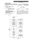
1
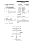
USOO8868802B2
(12) United States Patent
(10) Patent N0.:
Barten
(54)
(45) Date of Patent:
Oct. 21, 2014
METHOD ()1? PROGRAMMING THE
6,612,495 B2 *
DEFAULT CABLE INTERFACE SOFTWARE
6,707,581 B1 *
3/2004 Browning
IN AN INDICIA READING DEVICE
6,719,202 B1 *
4/2004 Kawai 6161.
6,877,663 B2*
4/2005
7,044,383 B2 *
7,104,456 B2
5/2006 Zhu et a1. ............... .. 235/462.46
9/2006 Parker et 31.
(75)
Inventor:
(73)
Assignee. Hand Held Products, Inc., Fort M111,
~
6,619,549 B2 *
Henri Barten, Limburg (BE)
.
-
7,389,918 B2
SC (Us)
Notice:
Subject to any disclaimer, the term of this
2007/0228137 A1
2008/0228773 A1*
Y
Y -
Kelly et al.
2008/0307197 A1
11/2010
""" n 358/473
.. 235/462.13
.... .. 235/462.15
Wike, Jr. et a1.
10/2009 Rathus 6161.
2008/0230607 A1
-
6/2008
Zhu et a1. ............... .. 235/462.45
7,600,691 B2
U S C 15403) b 176 da S
~
9/2003
10/2008 Bhella et al‘
patent is extended or adjusted under 35
-
9/2003 Reddersen et a1. .... .. 235/462.15
7,438,217 B2
7,837,111 B2 *
(*)
US 8,868,802 B2
Yang et a1. ............. .. 235/462.13
10/2007 Bhella et a1.
9/2008 Stewart et a1. ................ .. 707/10
9/2008 Etten
12/2008
2009/0048870 A1*
2/2009
Calvm 6161.
Godshallet al. ................ .. 705/3
(21)
App1.No.: 12/578,635
2009/0078773 A1
3/2009 Carlson 6161.
2009/0108067 A1*
4/2009
(22)
Filed;
2009/0200380 A1
8/2009 Longacre, Jr. et a1.
2009/0237221 A1
9/2009 Battles et a1.
Oct, 14, 2009
(65)
Prior Publication Data
US 2011/0087810 A1
FOREIGN PATENT DOCUMENTS
Apr. 14, 2011
WO
(51)
Roquemore ........... .. 235/462.15
Int. Cl.
*
6an 13/12
(2006.01)
G06K 7/10
G06K 7/00
(200601)
(200601)
2009064759
-
5/2009
-
med by exammer
Primary Examiner * Titus Wong
(74) Attorney, Agent, or Firm * Additon, Higgins &
(52) U-s- Cl-
Pendleton, P.A.
CPC ........ .. G06K 7/0004 (2013.01); G06K 7/10881
(2013.01); G06K 2207/1017 (2013.01)
(58)
(57)
ABSTRACT
USPC ......... .... ...... ... .................. .. 710/62; 236/462.14
An indicia reading apparatus includes an interconnect cable
Fleld 0f Classmeatlen search
CPC
G06F 17/00; G06K 7/10
and an indicia reading device. The indicia reading device is
con?gured so that, if the indicia reader device is not con?g
See apphcatlon
.... ..............................
?le fOr COmP16Ie.. seafCh hISIOI‘y-
ured
does to
notany
contain
interconnect
one of a cable
plurality
andof
detects
speci?ed
an indicia
sequences of
_
References Clted
data elements that the indicia reading device Will recognize
and use to con?gure itself to operate With the interconnect
cable, the indicia reading device Will indicate to the user of the
indicia reading device that the indicia reading device needs to
be con?gured to operate With the interconnect cable.
(56)
U.S. PATENT DOCUMENTS
5,424,524 A *
6/1995
6,293,467 B1
9/2001 Reddersen et a1.
Ruppert et a1. ............... .. 705/17
6,415,978 B1*
7/2002
17 Claims, 12 Drawing Sheets
McAllister ............. .. 235/46201
Power-Up Scanner
‘
230
234
232
lm
Default Variable
F llled'?
Indicate To User
That Scanner is
7 N01 Reaw For
236
Scanning
238
Fill the
De1ault
lnte?ace
Variable
y
240
Idle, Ready to Scan
US. Patent
0a. 21, 2014
Sheet 1 0112
US 8,868,802 B2
FIG.
1
136
130 134
1 2x“
128
118
122
12
126
120
US. Patent
Oct. 21, 2014
US 8,868,802 B2
Sheet 2 0f 12
EoL"cmos>Ez2Jm=E §mQ58|?r.
"rmungloLwHmvcnmoVFw:;O g.m
gLeomwAowIi Y
m_g6$3E:0w.25u869120w
oa2nb:B@o2EA895:muI0EN?2
49?an5owm@/egvac:2ohme6w1
ma\,/J
:MHa- AHlr.Lv
23ELz98w"0Ua254|Alo.?n0swao
2a9":2&538.50“25-wA!Al0w
9<unAl"809>%5:3I2E$v:w<
._o?z1"wm n_
-.E"FOWL50m1_6
wm"o?“mQE6otBw>$E“im:6a?wnmeE
"
“E
gH
/
n#9
mm?
__
mm:P
"“oweI"
:[ _
\gwt620a__Em:
o
6&3HnBEE »
1W.9L.
US. Patent
Oct. 21, 2014
US 8,868,802 B2
Sheet 3 0f 12
502m mow
wow
wow
8N
war
2
l m“au/m‘8a6!
m
o
w
l
NR)
2:8Em a
N:
vmr
469.
Fon
SNmm:02
@52\8r1
US. Patent
Oct. 21, 2014
US 8,868,802 B2
Sheet 4 0f 12
mFOEm mOwMG E
wow
wow
mom
mm?
.520
.QEmm
:1 w>ao
Fz4_<QOJ
com09‘
Hwoz
mow
KMszA\m@w
US. Patent
Oct. 21, 2014
US 8,868,802 B2
Sheet 5 0f 12
50 m mOw o
wow
wow
mom
.2 8
I. mama
.2$09
OONom
w
Pon
mewo
$5\@2
/
v2
mm?
US. Patent
Oct. 21, 2014
US 8,868,802 B2
Sheet 6 0f 12
502m mow u
Now
2
.Gm0_n_
w
25
wo._>w_>Oo<|Ew6
RN
8N
0
N:
F
x“
#09.
mow l
Go: w?8w.2: I mQHa<moa> 2
152\@2%
US. Patent
0a. 21, 2014
Sheet 7 0f 12
US 8,868,802 B2
Power-Up Scanner
230
Begin
Boot
Sequence
234
Indicate To User
Has an
Interface
That Scanner '5
FDl lndicia
Default Variable
NOt Ready For
Been
Filled?
Norm?|
Scanning
Scanned?
236
YES
238
Fill the
Default
interface
Variable
240
Load Interface
Default and
Continue
Boot
Fl G I 4A
Sequence
ldle‘ Ready to Scan
US. Patent
0a. 21, 2014
Sheet 8 0f 12
US 8,868,802 B2
Power-Up Scanner
- 234
Indicate To User
That Scanner is
——-} Not Ready For
Norm-8|
Scannlng
Begin
Boot
Sequence
Has all
236
FDI Ind|0|a
Been
Scanned?
242
Boot to a First
238
Con?guration
Fill the
Default
Interface
Variable
244
Load
Interface
Default
Boot to a
Second
Con?guration
Idle, Ready to Scan
FIG. 4B
US. Patent
0a. 21, 2014
Sheet 9 0f 12
US 8,868,802 B2
FIG.5
US. Patent
0a. 21, 2014
Sheet 10 0f 12
US 8,868,802 B2
Standard USB-Cable
Cable PN# 42206161-01E
i l i i il li lili lilili l lil i lil lil l lil l il lililil ili il i
IMPORTANT NOTICE
Please be notified when you do use your bar
code reader for the first time it will beep and
flash the Ieds to let you know its default
interface requires to be configured
To set the default interface to match the cable in
this bag, scan the bar code below
Set Default Interface to USB PC Ke board
254
For more detailed instructions refer to the First Time Usage
section in the user manual or Quick Start Guide
FIG. 6
/ 252
US. Patent
0a. 21, 2014
Sheet 11 0112
US 8,868,802 B2
FIG.7
US. Patent
0a. 21, 2014
Sheet 12 0112
US 8,868,802 B2
Standard USB-Cable
Cable PN# 42206161-01E
lil ilililil l il i il li l lili lil lili ili il i l ilil il l i l
IMPORTANT NOTICE
Please be notified when you do use your bar
code reader for the first time it will beep and
?ash the leds to let you know its default
interface requires to be configured
To set the default interface to match the cable in
this bag, read the RFID tag below
Set Default Interface to USB PC Keyboard
/ 272
For more detailed instructions refer to the First Time Usage
section in the user manual or Quick Start Guide
FIG. 8
/ 270
US 8,868,802 B2
1
2
METHOD OF PROGRAMMING THE
DEFAULT CABLE INTERFACE SOFTWARE
IN AN INDICIA READING DEVICE
cable if the indicia reader device detects an indicia which does
not contain a speci?ed sequence of data elements that the
FIELD OF THE INVENTION
in the interconnect cable with the speci?ed sequence of bar
data elements.
In still another form, the invention includes a method for
indicia reading device will recognize and con?gure itself to
operate with the interconnect cable, and an indicia with, on or
This invention relates to indicia reading devices, and more
particularly to a method of programming the default cable
interface software in an indicia reading device.
requiring a user of an indicia reader device to initially con
?gure the indicia reader device for operating with an inter
connect cable. The method comprises the steps of con?guring
BACKGROUND OF THE INVENTION
the indicia reader device so that if the indicia reader device
detects an indicia which does not contain one of a plurality of
Indicia reading devices (also referred to as optical indicia
speci?ed sequences of data elements that the indicia reading
readers, scanners, RFID readers, etc.) typically read indicia
data represented by printed indicia or data carrier indicia,
(also referred to as symbols, symbology, bar codes, RFID
device will recognize and use to con?gure itself to operate
with the interconnect cable, the indicia reading device will
indicate to the user of the indicia reading device that the
indicia reading device needs to be con?gured to operate with
the interconnect cable, and providing an indicia with an inter
connect cable which includes one of the plurality of speci?ed
sequences of data elements which is applicable to the inter
tags, etc.) For instance one type of a symbol is an array of
rectangular bars and spaces that are arranged in a speci?c way
to represent elements of data in machine readable form.
Another type of symbol is encoded as data in an RFID tag.
Optical indicia reading devices typically transmit light onto a
symbol and receive light scattered and/or re?ected back from
a bar code symbol. The received light is interpreted by an
image processor to extract the data represented by the sym
bol. Laser indicia reading devices typically utilize transmitted
laser light. RFID readers typically activate RFID tags which
20
connect cable.
BRIEF DESCRIPTION OF THE DRAWINGS
25
transmit data symbols to the RFID readers.
One-dimensional (1D) optical bar code readers are char
conjunction with the accompanying drawings, in which:
acterized by reading data that is encoded along a single axis,
in the widths of bars and spaces, so that such symbols can be
The aforementioned and other features, characteristics,
advantages, and the invention in general will be better under
stood from the following more detailed description taken in
30
FIG. 1 is a partial cutaway view of an optical indicia reader
in accordance with at least one embodiment of the present
read from a single scan along that axis, provided that the
invention;
symbol is imaged with a suf?ciently high resolution along
FIG. 2 is a block diagram of the optical indicia reader of
FIG. 1;
FIGS. 3A, 3B, 3C, and 3D are block diagrams of typical
data processing systems with which the reading device shown
that axis.
In order to allow the encoding of larger amounts of data in
a single bar code symbol, a number of 1D stacked bar code
35
symbologies have been developed which partition encoded
data into multiple rows, each including a respective lD bar
in FIG. 1 may be used;
FIGS. 4A and 4B are ?ow charts of alternate procedures for
code pattern, all or most all of which must be scanned and
initially con?guring the reading device shown in FIG. 1;
decoded, then linked together to form a complete message.
Scanning still requires relatively higher resolution in one
FIG. 5 is a perspective view on an interconnect cable in a
40
device shown in FIG. 1;
FIG. 6 is an enlarged view of the label shown in FIG. 5;
dimension only, but multiple linear scans are needed to read
the whole symbol.
A class of bar code symbologies known as two dimensional
(2D) matrix symbologies have been developed which offer
orientation-free scanning and greater data densities and
capacities than lD symbologies. 2D matrix codes encode data
FIG. 7 is a perspective view on an interconnect cable in a
45
matrix, accompanied by graphical ?nder, orientation and ref
erence structures.
50
It will be appreciated that for purposes of clarity and where
deemed appropriate, reference numerals have been repeated
in the ?gures to indicate corresponding features. Also, the
relative size of various objects in the drawings has in some
which directly controls the operations of the various electrical
components housed within the indicia reader. For example,
the central processor controls detection of keyboard entries,
display features, trigger detection, and indicia read and
decode functionality.
plastic bag with an embedded RFID tag for initially con?g
uring the reading device shown in FIG. 1; and
FIG. 8 is an enlarged view of a label for a bag containing an
interconnect cable which includes a RFID tag in the label.
as dark or light data elements within a regular polygonal
Conventionally, an indicia reader, whether portable or oth
erwise, optical or wireless, may include a central processor
plastic bag with a label for initially con?guring the reading
cases been distorted to more clearly show the invention.
DETAILED DESCRIPTION
55
Efforts regarding such systems have led to continuing
Reference will now be made to exemplary embodiments of
the invention which are illustrated in the accompanying draw
developments to improve their versatility, practicality and
ings. This invention, however, may be embodied in various
ef?ciency.
forms and should not be construed as limited to the embodi
60
SUMMARY OF THE INVENTION
ments set forth herein. Rather, these representative embodi
ments are described in detail so that this disclosure will be
thorough and complete, and will fully convey the scope,
The invention comprises, in one form thereof, an indicia
structure, operation, functionality, and potential of applica
scanning apparatus including an interconnect cable, an indi
cia reading device con?gured to provide an indication to a
user of the indicia reading device that the indicia reading
bility of the invention to those skilled in the art.
Referring to FIG. 1, an exemplary hand held indicia read
device needs to be con?gured to operate with an interconnect
65
ing device or scanner 112 (referred to as “scanner 112”) has a
number of subsystems for capturing images, interrogating
US 8,868,802 B2
3
4
RFID tags, and decoding dataforrns within such images and
patterns are possible and not limited to any particular pattern
or type of pattern, such as any combination of rectilinear,
tags. The scanner 112 has an imaging reader assembly 114, an
electronics assembly 116, an inner cable 118 from the elec
tronics assembly 116 to a connector (not shown) at the end of
a handle 120, and two LEDs, 122 and 124, positioned behind
translucent windows 126, and a housing 128 which encloses
the electrical parts and is connected to the handle 120. The
electronics assembly includes an RFID assembly 130, a
vibrator 132, and a sound generator 134. A trigger 136 is used
linear, circular, elliptical, etc., ?gures, whether continuous or
discontinuous, i.e., de?ned by sets of discrete dots, dashes,
5
light source which is su?iciently small or concise and bright
to provide a desired illumination pattern at the target. For
example, the aimer light source 164 may comprise one or
more LEDs, such as part number NSPG3 00A made by Nichia
to activate and deactivate the scanner 112.
Referring to FIG. 2, the image reader assembly 114 and
electronics assembly 116 generally comprises a receive opti
cal system 140, an illumination assembly 150, an aiming
Corporation. Illumination and aiming light sources with dif
ferent colors and combination of colors may be employed, for
example white, green and red LEDs. The colors may chosen
based on the color of the symbols most commonly imaged by
the image reader. Different colored LEDs may be each alter
pattern generator 160, an RFID reader unit 170, and a variety
of control and communication modules. The receive optical
system 140 generates frames of data containing indications of
the intensity of light received by the read optical system 140.
natively pulsed at a level in accordance with an overall power
The illumination assembly 150 illuminates a target T creating
re?ections that are received by the receive optical system 140.
The aiming pattern generator 160 projects an aiming light
and the like. Alternately, the aimer pattern generator may be a
laser pattern generator.
Generally, the aimer light source 164 may comprise any
budget.
20
The aimer light sources 164 may also be comprised of one
pattern to assist with aiming the scanner 112. While the
or more laser diodes such as those available from Rohm. In
present description employs an imager based data collection
this case a laser collimation lens (not shown in these draw
subsystem (the image reader assembly 114 and electronics
ings) will focus the laser light to a spot generally forward of
the scanning head and approximately at the plane of the target
assembly 116), it is to be recognized that the data collection
subsystem may take other forms such as a laser scanner.
25
The receive optical system 140 generally comprises image
receive optics 142 and an image sensor 144. The image optics
142 receives light re?ected from a target T and projects the
re?ected light on to the image sensor 144. The image sensor
144 may comprise any one of a number of two-dimensional,
color or monochrome solid state image sensors using such
30
etc. One possible sensor is the MT9V022 sensor from Micron
Technology Inc. Such sensors contain an array of light sen
and an RFID antenna 176. The RFID reader unit 170 may be
35
energy into electric charges.
Many image sensors are employed in a full frame (or
global) shutter operating mode, wherein the entire imager is
reset prior to an image capture operation to remove any
residual signal in the photodiodes. The photodiodes (pixels)
period (time during which light is collected), all charges are
45
sor. The light shield prevents further accumulation of charge
during the readout process. The signals are then shifted out of
the light shielded areas of the sensor and read out. Image
sensor 144 may also employ a rolling shutter.
The illumination assembly 150 generally comprises a
con?gured to read RF encoded data from a passive RFID tag,
such as tag 262 (FIG. 7). Where RFID reader unit 170 is
con?gured to read RF encoded data from a passive RFID tag
262, RP oscillator and receiver circuit 174 transmits a carrier
signal from antenna 176 to passive tag 262. Passive RFID tag
262 converts the carrier energy to voltage form and a tran
40
then accumulate charge for some period of time (exposure
period), with the light collection starting and ending at about
the same time for all pixels. At the end of the integration
simultaneously transferred to light shielded areas of the sen
items and may be purchased, for example, from Digital
Optics Corp. of Charlotte, NC. among others.
The RFID reader unit 170 generally comprises an RFID
data processing circuit 172, an RF oscillator and receiver 174,
technologies as CCD. CMOS, NMOS, PMOS, CD, CMD,
sitive photodiodes (or pixels) that convert incident light
T. This beam may then be imaged through a diffractive inter
ference pattern generating element, such as a holographic
element fabricated with a desired pattern in mind. Examples
of these types of elements are known, commercially available
sponder of tag 262 is actuated to transmit a radio signal
representing the encoded tag data. RF oscillator and receiver
circuit 174, in turn, receives the radio signal from the tag and
converts the data into a digital format. RFID data processing
circuit 172, typically including a low cost microcontroller IC
chip, decodes the received radio signal information received
by RF oscillator and receiver circuit 147 to decode the
encoded identi?cation data originally encoded into RFID tag
262. The decoded digital data is passed to bus 18211.
A scanner processor 180 provides overall control of the
50
image reader assembly 114 and electronics assembly 116.
power supply 152, an illumination source 154 and illumina
The scanner processor 180 and other components of the
tion optics 156. The illumination optics 156 directs the output
image reader assembly are generally connected by one or
of the illumination source 154 (generally comprising LEDs or
more buses 182n and/or dedicated communication lines. In
the illustrated example a parallel bus 182a connects the scan
the like) onto the target T. The light is re?ected off the target
T and received by the receive optical system 140. It is to be
noted that the illumination provided by the illumination
55
ner processor 180 to a cable interface circuit 183 which
includes a cable connector and to a main system memory 184
assembly 150 may be combined with (or replaced by) other
used to store processed (and unprocessed) image data from
sources of illumination, including ambient light from sources
the image sensor 144. The scanner processor 180 utilizes an
I2C bus 182!) to communicate exposure settings to the image
outside of the scanner 112.
The aiming pattern generator 160 generally comprises a
60
ates an aiming light pattern projected on or near the target
which spans a portion of the receive optical system’s 140
operational ?eld of view with the intent of assisting the opera
sensor 144 and illumination parameters to a microcontroller
186. A dedicated 8 to 10 bit parallel bus 1820 is used to
transfer image data from the image sensor 144 to the scanner
processor 180. The width of the bus 1820 may be dependant
on the bit size recorded by each pixel in the image sensor 144.
power supply 162, an aimer light source 164, an aperture 166,
and aimer optics 168. The aiming pattern generator 160 cre
65
The output of the image sensor 144 is processed by the scan
tor to properly aim the scanner at the bar code pattern that is
ner processor 180 utilizing one or more functions or algo
to be read. A number of representative generated aiming
rithms, which may be stored in an EEPROM 187, to condition
US 8,868,802 B2
5
6
the signal appropriately for use in further processing down
power supply 216 is connected to a power connector 217
which, in turn, is connected to the connector 218 which
replaces the connector 212 in FIG. 3A. In FIG. 3D the scanner
112 is connected by an interconnect cable 219 directly to a
local area network (LAN) 220, such as an ETHERNET LAN,
which is also connected to the local host processor 190. The
interconnect cable 219 couples the scanner 112 to the LAN
220 at a LAN connector 222. Power supply 216 connected to
a power connector 217 which, in turn, is connected to the
LAN connector 222 to provide power to the scanner 112.
In the past scanners may have been preprogrammed to
operate with a speci?c interface cable which may be part of a
scanner kit. However, in some cases the preprogrammed
scanner does not match the interconnect cable in the kit. For
example, a customer may buy a USB kit, but the scanner is
stream, including being digitized to provide a digitized image
of target T.
Another function of the scanner processor 180 is to decode
machine readable symbology represented within an image
captured by the image sensor 144. Information respecting
various reference decode algorithms is available from various
published standards, such as by the International Standards
Organization (“ISO”). The scanner processor 180 also con
trols the scanner housing status indicator device drivers 189
which drives the LEDs 122 and 124, the vibrator 132, and the
sound generator 134.
The microcontroller 186 maintains illumination param
eters, used to control operation of the illumination assembly
150 and the aiming pattern generator 160, in a memory 188.
For example, the memory 188 may contains tables indicative
of power settings for the power supplies 152 and 162 corre
sponding to various states of the signal from the image sensor
144. Based upon signals from the scanner processor 180
and/or the image sensor 144, the microcontroller 186 sends
signals to the power supplies 152 and 162 based on values
stored in the table in memory 188. An exemplary microcon
troller 150 is the CY8C24223A made by Cypress Semicon
programmed for a keyboard wedge, and consequently the
scanner does not work “out of the box.” Once connected, the
scanner seems to be ready and there is no indication that
further setup is required. The problem is that in mass produc
20
ductor Corporation.
FIGS. 3A, 3B, 3C, and 3D are four block diagrams of
exemplary systems with which the scanner 112 may be used.
Although the optical scanner 112 is used in the drawings, a
wireless or RFID scanner may also be used with the present
invention. In FIG. 3A the scanner 112 is coupled to a local
host processor 190 by means an interconnect cable 192,
which in FIG. 3A may have a USB connection to the host
processor 190. Host processor 190 may be connected to a
display 194, to a printer 196, and a keyboard 198. As used
herein, the term “local host processor” will be understood to
include both stand alone host processors and host processors
which comprise only one part of a local computer system.
If the software for the scanner 112 is available locally as,
for example, on a diskette or CD-ROM, it may be loaded
using a suitable drive unit 200. The local host processor 190
may be in communication with a remotely located processor
202 through a suitable transmission link 204, such as an
electrical conductor link, a ?ber optic link, or a wireless
transmission link through a suitable communication interface
206, such as a modem. As used herein, the term “transmission
link” will be understood to refer broadly to any type of trans
25
30
cannot provide the power needed by the scanner 112. For
example, a serial port on the host processor 190 is a connec
tion which cannot power the scanner 112. In FIG. 3C a sepa
rate power supply 216 is needed for the scanner 112. The
ner 112 by an end user for a particular type of interconnect
cable when the scanner 112 is in a “boot mode new” (BMN)
mode meaning that an interface default variable has not been
set, and there is no interconnection cable con?guration set in
the scanner 112. Turning to FIG. 4A, whenever the scanner
112 is powered up while in the BMN mode, an initial boot
sequence is performed as indicated in box 230. The boot
35
40
45
sequence includes a test of the interface default variable to
determine if it is ?lled as shown in box 232. If the interface
default variable has not been ?lled, the scanner 112 indicates
to the user that the variable has not been ?lled as shown in box
234. The indication may be illumination of one or both of the
LEDs 122, 124 shown in FIG. 1, either constantly or inter
mittently. The indication may also be a sequence of prere
corded sounds generated by the sound generator 134 and/or a
movement in the scanner 112 by the vibrator 132. In addition,
since the scanner 112 has not completed the boot sequence in
the embodiment shown in FIG. 4, the scanner 112 will not be
con?gured to read and interpret product indicia, such as bar
codes and RFID tags, or perform any other functions that the
scanner is capable of when it has completed the boot
an RF link, or a computer network, e.g., ETHERNET
infrared or microwave communication link. Link 204 could
also be an acoustic communications link.
The connection to the host processor 190 must be of a type
to provide electrical data between the scanner 112 and the
host process 190, and provide power to the scanner 112. A
USB connection can perform these functions, as can a key
board connection. FIG. 3B shows the scanner 112 connected
to the host processor 190 by an interconnection cable 213
with a keyboard wedge 214 at one end to permit the use of a
keyboard with the scanner 112. In FIG. 3C the scanner 112 is
connected to the host processor 190 by an interconnect cable
215 at a connection 218 to the host processor 190 which
scanners is that if the “factory defaults” indicia is scanned, the
scanner defaults to the device’s default interface, which isn’t
necessarily the interface the user requires or expects.
FIGS. 4A and 4B are ?ow diagrams showing alternate
embodiments of the steps used to initially con?gure the scan
mission facility, including an RS-232 capable telephone line,
although other types of transmission links or networks may
also be used. For example, transmission link 204 could be
provided by a coaxial cable or any other non-RF electromag
netic energy communication link including a light energy
tion the manufacturer sometimes does not know in what kit a
scanner will end up. Another downside of the preprogrammed
sequence. The scanner 112 than waits until a ?ash default
50
interface (FDI) indicia is received as indicated in box 236.
The FDI indicia provides software commands which the
scanner 112 uses to con?gure itself to an interconnect cable
associated with the FDI indicia. After the FDI indicia is
detected, the scanner ?lls the interface default variable as
shown in box 238, and resumes the boot sequence including
55
loading the interface default programmed in the FDI indicia
as shown in box 240.
In FIG. 4B the scanner 112 begins a boot sequence as
60
indicated by box 230 and then checks to see if the interface
default variable is set in box 232. If the interface default
variable has not been set, then the scanner 112 continues
booting up to a ?rst con?guration indicated by box 242 and
then signals an operator, either continuously or intermittently,
in the manner described above, to scan a FDI indicia as
indicated by box 234. While the scanner 112 is signaling the
65 user to scan a FDI indicia, the scanner 112 tests whether a FDI
indicia has been scanned in box 236. Once a FDI indicia has
been scanned, the interface default variable is ?lled as indi
US 8,868,802 B2
7
8
cated in box 238 and the interface default is loaded into the
signal from each RFID tag responding to the RFID reader,
memory of the scanner 112 as indicated in box 244. Then the
and ignore FDI RFID tags unless the scanner 112 does not
boot sequence is restarted as indicated in box 230, and
whether or not the interface default variable has been set is
have a con?gured cable interface or the scanner 112 has been
pro grammed to receive a new default cable interface from an
once more been tested as indicated in box 232. Since the
interface default variable has been set, the scanner 112 con
FDI RFID tag.
While the invention has been described with reference to
tinues booting up to a second con?guration as indicated in
particular embodiments, it will be understood by those skilled
box 246. At this time the scanner 112 goes into an idle state
in the art that various changes may be made and equivalents
may be substituted for elements thereof without departing
from the scope of the invention. In addition, many modi?ca
waiting to scan and attempt to interpret any indicia.
After the initial interconnection cable con?guration has
been set, the interconnect cable interface may be changed to
allow the scanner 112 to operate with other interface cables
using programming indicia listed in a user’s instruction
tions may be made to adapt a particular situation or material
to the teachings of the invention without departing from the
scope of the invention.
Therefore, it is intended that the invention not be limited to
the particular embodiments disclosed as the best mode con
manual. However, changing the interconnect interface in this
manner may not change the interface default variable, and if
a master reset indicia is scanned, the interconnect cable inter
face may revert to the initial interconnection cable con?gu
templated for carrying out this invention, but that the inven
tion will include all embodiments falling within the scope and
spirit of the appended claims.
ration. Thus, if a user sets the default interface variable with a
FDI indicia for a USB cable, later changes to an interconnect
cable con?guration for a keyboard wedge by scanning the
The invention claimed is:
20
1. A method for requiring a user of an indicia reader device
indicia for a keyboard wedge interconnect cable in the user’ s
to initially con?gure the indicia reader device for operating
manual, and then later scans a master reset indicia, the scan
ner 112 may revert back to the USB interconnect cable con
with an interconnect cable comprising the steps of:
con?guring the indicia reader device with factory defaults;
?guration.
However, the manufacturer may provide a hidden com
mand available to the manufacturer’s support personnel to
erase the interconnection cable con?guration putting the
25
scanner back into the BMN mode. The user would then have
to set the default interface variable using a process such as
those shown in FIG. 4A or 4B. By resetting the FDI variable,
30
reading device electronically indicating to the user that
the indicia reading device needs to be con?gured to
interface cable con?guration.
35
code in order to work with a basic scanner 112 which can only
read linear (1D) bar codes.
FIG. 5 is a perspective view of the interconnect cable 192
in a plastic bag 250 with a label 252 with a FDI bar code 254
to be used for initially con?guring the scanner 112 so that it is
compatible with the cable 192. The label 252 that instructs the
factory default interconnect cable;
40
2. The method set forth in claim 1, further including the
steps of resetting the interface variable when the indicia
reader device reads indicia that contains a reset interface
45
variable program or receives a reset interface command via an
already established interface connection.
that it is compatible with the cable 260.
50
55
60
3. The method set forth in claim 2 wherein the reset inter
face variable program data elements are not made generally
available to users of the indicia reader device.
4. The method set forth in claim 1 wherein a reset to factory
defaults program causes the indicia reader device to con?gure
itself to operate with the interconnect cable associated with
the indicia previously read or received which last set the
interface variable to the second state.
5. The method set forth in claim 1 wherein the indicia
reader device boots to a ?rst con?guration when the interface
variable is in the ?rst state, and boots to a second con?gura
tion when the interface variable is in the second state.
6. A method for con?guring an indicia reader for operating
with a factory default interconnect cable comprising the steps
of:
setting an interface variable to a ?rst status prior to ship
ping the indicia reader to a user such that the indicia
reader is not operable to read indicia that is not one of a
an Application Family Identi?er (AFI) which is different
from the AFI of other RFID tags that are not used to con?gure
the cable interface of the scanner 112. The RFID reader in the
scanner 112 would therefore recognize the AFI of transmitted
receiving a speci?ed sequence of data elements; and
restoring the disabled functionality.
RFID tag 264 embedded in a connector 266 of the cable 260
which can be used for initially con?guring the scanner 112 so
FIG. 8 shows a label 270 which includes a RFID tag 272
and can be placed on the plastic bag 262 for an interconnect
cable which may not have an imbedded RFID tag in the
interconnect cable. The label 270 may be used with intercon
nect cables, such as an USB interconnect cable, which is used
with scanners 112 which have different interface con?gura
tions. However, there may be some cables which are used
only with scanners with the same designated cable interface,
and the embedded RFID tag could be used.
The RFID tags 264 and 272 are FDI RFID tags in that they
are used to initially con?gure the interconnect cables 260 and
272. Because the RFID tag 264 embedded in the cable con
nector 266 may respond to the RFID reader in the scanner 1 12
after it has been con?gured and will therefore broadcast its
data, the FDI RFID tags 264, 272 may be encoded to transmit
operate with the recognized interconnect cable;
disabling functionality of the indicia reader device that is
not the reading functionality of the indicia reader device
until the indicia reader device receives a speci?ed
sequence of data elements which is applicable to the
user to scan the indicated bar code 254 on the label before
trying to use the scanner 112 is shown in FIG. 6.
FIG. 7 is a perspective view of the interconnect cable 260
in aplastic bag 262, similar to that shown in FIG. 5, with a
of speci?ed sequences of data elements that the indicia
reading device will recognize a factory default intercon
nect cable;
responsive to the boot sequence executing and determining
that the interface default variable is not set, the indicia
the scanner 112 would then be ready for sale to anew user or
for use in a different location in a company, and the master
reset command would not cause an unwanted change in the
The FDI indicia on the cable-bag may be a linear (1D) bar
executing an initial boot sequence that includes a test for
the presence of an interface default variable so that if the
indicia reader device does not contain one of a plurality
65
plurality of interface con?guration indicia;
providing the interface factory default interconnect cable
with an indicia which contains one of the plurality of
US 8,868,802 B2
10
interface con?guration data elements prior to shipping
9. The indicia reader device set forth in claim 8, wherein the
indicia reader device is con?gured to read a linear bar code
when the indicia reader device is in a lower functional state.
10. The indicia reader device set forth in claim 8, wherein
the interface variable can be reset by reading a reset interface
variable program data carrier after the interface variable has
the factory default interconnect cable to the user;
executing an initial boot sequence that includes a test of the
interface variable; and
setting the interface variable to a second status upon read
ing one of the plurality of interface con?guration data
elements if the indicia reader needs to be con?gured to
operate with the interconnect cable based on the test,
wherein the functionality of the indicia reader is limited
when the interface variable is in the second status, and
wherein during the initial boot sequence the indicia reader
will electronically indicate to the user of the indicia
reader that the indicia reader needs to be con?gured to
operate with the interconnect cable.
7. The method set forth in claim 6 further including the step
of resetting the interface variable to the ?rst status after the
been set.
11. The indicia reader device set forth in claim 8 wherein a
reset to factory defaults program causes the indicia reader
device to con?gure itself to operate with the interconnect
cable associated with the indicia previously read which last
set the interface variable to the second state.
12. The indicia reader device set forth in claim 8 wherein
the indicia reader device is con?gured to boot to a ?rst con
?guration when the interface variable is ab sent, and to boot to
a second con?guration when the interface variable is present.
13. The method set forth in claim 1, wherein the indication
interface variable has been set to the second status.
8. An indicia reader device con?gured to perform a method
is at least one of the following: illumination of one or more
comprising:
executing an initial boot sequence that includes a test of the
light emitting diodes(s); a sequence of prerecorded sounds
20
indicia reader device con?guration wherein the initial
boot sequence comprising a detecting the presence or
absence of an interface default variable;
providing an indication to a user of the indicia reading
device that if the indicia reading device is not con?gured
to operate with any interconnect cable responsive to
detecting that the initial interface default variable is
is at least one of the following: illumination of one or more
light emitting diodes(s); a sequence of prerecorded sounds
25
absent;
shifting the indicia reader device to a lower functional
state, responsive to detecting that the initial interface
default variable is absent;
self-con?guring to operate with an interconnect cable
elements on the interconnect cable and populating the
interface default variable; and,
restoring the indicia reading device to a normal functional
state, responsive to populating the interface default vari
able.
generated by a sound generator and movement of the indicia
device by a vibrator.
15. The indicia reader device set forth in claim 8, wherein
the indication is at least one of the following: illumination of
one or more light emitting diodes(s); a sequence of prere
30
wherein the interconnect cable includes a speci?ed
sequence of data elements and wherein the self-con?g
uring comprises reading the speci?ed sequence of data
generated by a sound generator and movement of the indicia
device by a vibrator.
14. The method set forth in claim 6, wherein the indication
35
corded sounds generated by a sound generator and movement
of the indicia device by a vibrator.
16. The method of claim 1, wherein the indicia reader
device is not con?gured to read and interpret product indicia
until the indicia reader device receives the speci?ed sequence
of data elements.
17. The indicia reader device of claim 8, wherein the restor
ing comprises con?guring the indicia reader device to read
and interpret product indicia.
*
*
*
*
*