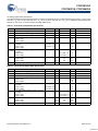
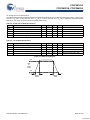
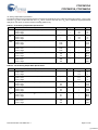
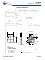
1
CY8C24123A
CY8C24223A, CY8C24423A
PSoC® Programmable System-on-Chip™
Features
■
■
■
■
■
Powerful Harvard Architecture Processor
❐ M8C Processor Speeds to 24 MHz
❐ 8x8 Multiply, 32-Bit Accumulate
❐ Low Power at High Speed
❐ 2.4 to 5.25V Operating Voltage
❐ Operating Voltages Down to 1.0V Using On-Chip Switch
Mode Pump (SMP)
❐ Industrial Temperature Range: -40°C to +85°C
Advanced Peripherals (PSoC Blocks)
❐ Six Rail-to-Rail Analog PSoC Blocks Provide:
• Up to 14-Bit ADCs
• Up to 9-Bit DACs
• Programmable Gain Amplifiers
• Programmable Filters and Comparators
❐ Four Digital PSoC Blocks Provide:
• 8 to 32-Bit Timers, Counters, and PWMs
• CRC and PRS Modules
• Full-Duplex UART
• Multiple SPI™ Masters or Slaves
• Connectable to All GPIO Pins
❐ Complex Peripherals by Combining Blocks
■
New CY8C24x23A PSoC Device
❐ Derived From the CY8C24x23 Device
❐ Low Power and Low Voltage (2.4V)
■
Additional System Resources
2
❐ I C™ Slave, Master, and MultiMaster to 400 kHz
❐ Watchdog and Sleep Timers
❐ User-Configurable Low Voltage Detection
❐ Integrated Supervisory Circuit
❐ On-Chip Precision Voltage Reference
■
Complete Development Tools
❐ Free Development Software (PSoC Designer™)
❐ Full-Featured, In-Circuit Emulator, and Programmer
❐ Full Speed Emulation
❐ Complex Breakpoint Structure
❐ 128K Trace Memory
Logic Block Diagram
Port 2 Port 1 Port 0
System Bus
Precision, Programmable Clocking
❐ Internal ±2.5% 24/48 MHz Oscillator
❐ High accuracy 24 MHz with optional 32 kHz Crystal and PLL
❐ Optional External Oscillator, up to 24 MHz
❐ Internal Oscillator for Watchdog and Sleep
Global Digital Interconnect
SRAM
256 Bytes
Global Analog Interconnect
SROM
Flash 4K
CPU Core (M8C)
Interrupt
Controller
Flexible On-Chip Memory
❐ 4K Flash Program Storage 50,000 Erase/Write Cycles
❐ 256 Bytes SRAM Data Storage
❐ In-System Serial Programming (ISSP)
❐ Partial Flash Updates
❐ Flexible Protection Modes
❐ EEPROM Emulation in Flash
Programmable Pin Configurations
❐ 25 mA Sink on all GPIO
❐ Pull Up, Pull Down, High Z, Strong, or Open Drain Drive
Modes on All GPIO
❐ Up to Ten Analog Inputs on GPIO
❐ Two 30 mA Analog Outputs on GPIO
❐ Configurable Interrupt on All GPIO
Analog
Drivers
PSoC CORE
Sleep and
Watchdog
Multiple Clock Sources
(Includes IMO, ILO, PLL, and ECO)
DIGITAL SYSTEM
ANALOG SYSTEM
Analog
Ref
Digital
Block
Array
Digital
Clocks
Multiply
Accum.
Decimator
Analog
Block
Array
I2C
POR and LVD
System Resets
Analog
Input
Muxing
Internal
Voltage
Ref.
Switch
Mode
Pump
SYSTEM RESOURCES
Cypress Semiconductor Corporation
Document Number: 38-12028 Rev. *I
•
198 Champion Court
•
San Jose, CA 95134-1709
•
408-943-2600
Revised December 11, 2008
[+] Feedback
CY8C24123A
CY8C24223A, CY8C24423A
The PSoC family consists of many Mixed-Signal Array with
On-Chip Controller devices. These devices are designed to
replace multiple traditional MCU-based system components with
a low cost single-chip programmable device. PSoC devices
include configurable blocks of analog and digital logic, and
programmable interconnects. This architecture enables the user
to create customized peripheral configurations that match the
requirements of each individual application. Additionally, a fast
CPU, Flash program memory, SRAM data memory, and
configurable IO are included in a range of convenient pinouts and
packages.
Digital System
The Digital System consists of 4 digital PSoC blocks. Each block
is an 8-bit resource that may be used alone or combined with
other blocks to form 8, 16, 24, and 32-bit peripherals, which are
called user module references.
Figure 1. Digital System Block Diagram
Port 1
Port 2
The PSoC architecture, shown in Figure 1, consists of four main
areas: PSoC Core, Digital System, Analog System, and System
Resources. Configurable global busing allows combining all the
device resources into a complete custom system. The PSoC
CY8C24x23A family can have up to three IO ports that connect
to the global digital and analog interconnects, providing access
to 4 digital blocks and 6 analog blocks.
8
8
PSoC GPIOs provide connection to the CPU, digital, and analog
resources of the device. Each pin’s drive mode may be selected
from eight options, allowing great flexibility in external
interfacing. Every pin can generate a system interrupt on high
level, low level, and change from last read.
Document Number: 38-12028 Rev. *I
Row 0
DBB00
DBB01
DCB02
4
DCB03
4
GIE[7:0]
GIO[7:0]
Global Digital
Interconnect
Row Output
Configuration
The PSoC device incorporates flexible internal clock generators,
including a 24 MHz IMO (internal main oscillator) accurate to
2.5% over temperature and voltage. The 24 MHz IMO can also
be doubled to 48 MHz for use by the digital system. A low power
32 kHz ILO (internal low speed oscillator) is provided for the
Sleep timer and WDT. If crystal accuracy is required, the ECO
(32.768 kHz external crystal oscillator) is available for use as a
Real Time Clock (RTC) and can optionally generate a
crystal-accurate 24 MHz system clock using a PLL. The clocks,
together with programmable clock dividers (as a System
Resource), provide the flexibility to integrate almost any timing
requirement into the PSoC device.
To Analog
System
DIGITAL SYSTEM
The PSoC Core is a powerful engine that supports a rich feature
set. The core includes a CPU, memory, clocks, and configurable
GPIO (General Purpose IO).
Memory encompasses 4 KB of Flash for program storage, 256
bytes of SRAM for data storage, and up to 2 KB of EEPROM
emulated using the Flash. Program Flash uses four protection
levels on blocks of 64 bytes, allowing customized software IP
protection.
To System Bus
Digital PSoC Block Array
PSoC Core
The M8C CPU core is a powerful processor with speeds up to
24 MHz, providing a four MIPS 8-bit Harvard architecture
microprocessor. The CPU uses an interrupt controller with
11 vectors, to simplify programming of real time embedded
events. Program execution is timed and protected using the
included Sleep and Watchdog Timers (WDT).
Port 0
Digital Clocks
From Core
Row Input
Configuration
PSoC® Functional Overview
8
8
GOE[7:0]
GOO[7:0]
Digital peripheral configurations are:
■
PWMs (8 to 32 bit)
■
PWMs with Dead band (8 to 24 bit)
■
Counters (8 to 32 bit)
■
Timers (8 to 32 bit)
■
UART 8 bit with selectable parity
■
SPI master and slave
■
I2C slave and multi-master (one is available as a System
Resource)
■
Cyclical Redundancy Checker/Generator (8 to 32 bit)
■
IrDA
■
Pseudo Random Sequence Generators (8 to 32 bit)
The digital blocks may be connected to any GPIO through a
series of global buses that can route any signal to any pin. The
buses also allow for signal multiplexing and performing logic
operations. This configurability frees your designs from the
constraints of a fixed peripheral controller.
Digital blocks are provided in rows of four, where the number of
blocks varies by PSoC device family. This gives a choice of
system resources for your application. Family resources are
shown in Table 1 on page 4.
Page 2 of 56
[+] Feedback
CY8C24123A
CY8C24223A, CY8C24423A
The Analog System consists of six configurable blocks, each
consisting of an opamp circuit that allows the creation of complex
analog signal flows. Analog peripherals are very flexible and can
be customized to support specific application requirements.
Some of the more common PSoC analog functions (most
available as user modules) are:
■
■
Analog-to-digital converters (up to two, with 6 to 14-bit
resolution, selectable as Incremental, Delta Sigma, and SAR)
Figure 2. Analog System Block Diagram
P0[7]
P0[6]
P0[5]
P0[4]
P0[3]
P0[2]
P0[1]
P0[0]
AGNDIn RefIn
Analog System
P2[3]
Filters (two and four pole band-pass, low-pass, and notch)
■
Amplifiers (up to two, with selectable gain to 48x)
■
Instrumentation amplifiers (one with selectable gain to 93x)
■
Comparators (up to two, with 16 selectable thresholds)
■
DACs (up to two, with 6 to 9-bit resolution)
■
Multiplying DACs (up to two, with 6 to 9-bit resolution)
■
High current output drivers (two with 30 mA drive as a PSoC
Core resource)
■
1.3V reference (as a System Resource)
■
DTMF Dialer
P2[1]
P2[6]
P2[4]
P2[2]
P2[0]
Array Input Configuration
ACI0[1:0]
ACI1[1:0]
Block Array
■
Modulators
ACB00
■
Correlators
ASC10
ASD11
■
Peak Detectors
ASD20
ASC21
■
Many other topologies possible
Analog blocks are arranged in a column of three, which includes
one CT (Continuous Time) and two SC (Switched Capacitor)
blocks, as shown in Figure 2.
ACB01
Analog Reference
Interface to
Digital System
RefHi
RefLo
AGND
Reference
Generators
AGNDIn
RefIn
Bandgap
M8C Interface (Address Bus, Data Bus, Etc.)
Document Number: 38-12028 Rev. *I
Page 3 of 56
[+] Feedback
CY8C24123A
CY8C24223A, CY8C24423A
Getting Started
Additional System Resources
System Resources, some of which are listed in the previous
sections, provide additional capability useful to complete
systems. Additional resources include a multiplier, decimator,
switch mode pump, low voltage detection, and power on reset.
Statements describing the merits of each system resource
follow:
■
Digital clock dividers provide three customizable clock
frequencies for use in applications. The clocks can be routed
to both the digital and analog systems. Additional clocks may
be generated using digital PSoC blocks as clock dividers.
■
A multiply accumulate (MAC) provides a fast 8-bit multiplier
with 32-bit accumulate, to assist in both general math and
digital filters.
■
The decimator provides a custom hardware filter for digital
signal processing applications including the creation of Delta
Sigma ADCs.
■
The I2C module provides 100 and 400 kHz communication over
two wires. Slave, master, and multi-master are supported.
■
Low Voltage Detection (LVD) interrupts can signal the application of falling voltage levels, while the advanced POR (Power
On Reset) circuit eliminates the need for a system supervisor.
■
An internal 1.3V reference provides an absolute reference for
the analog system, including ADCs and DACs.
■
An integrated switch mode pump (SMP) generates normal
operating voltages from a single 1.2V battery cell, providing a
low cost boost converter.
The quickest path to understanding the PSoC silicon is by
reading this data sheet and using the PSoC Designer Integrated
Development Environment (IDE). This data sheet is an overview
of the PSoC integrated circuit and presents specific pin, register,
and electrical specifications. For in-depth information, along with
detailed programming information, refer the PSoC Programmable Sytem-on-Chip Technical Reference Manual.
For up-to-date Ordering, Packaging, and Electrical Specification
information, refer the latest PSoC device data sheets on the web
at http://www.cypress.com/psoc.
Development Kits
Development Kits are available from the following distributors:
Digi-Key, Avnet, Arrow, and Future. The Cypress Online Store
contains development kits, C compilers, and all accessories for
PSoC development. Go to the Cypress Online Store web site at
http://www.cypress.com, click the Online Store shopping cart
icon at the bottom of the web page, and click PSoC (Programmable System-on-Chip) to view a current list of available items.
Technical Training
Free PSoC technical training is available for beginners and is
taught by a marketing or application engineer over the phone.
PSoC training classes cover designing, debugging, advanced
analog, and application-specific classes covering topics, such as
PSoC and the LIN bus. Go to http://www.cypress.com, click on
Design Support located on the left side of the web page, and
select Technical Training for more details.
Table 1. PSoC Device Characteristics
Technical Support
PSoC Part
Number
Flash
Size
Certified PSoC Consultants offer everything from technical
assistance to completed PSoC designs. To contact or become a
PSoC Consultant go to http://www.cypress.com, click on Design
Support located on the left side of the web page, and select
CYPros Consultants.
SRAM
Size
Depending on your PSoC device characteristics, the digital and
analog systems can have 16, 8, or 4 digital blocks, and 12, 6, or
4 analog blocks. Table 1 lists the resources available for specific
PSoC device groups. The PSoC device covered by this data
sheet is highlighted in this table.
Digital
Rows
Digital
Blocks
Analog
Inputs
Analog
Outputs
Analog
Columns
Analog
Blocks
Consultants
Digital
IO
PSoC Device Characteristics
PSoC application engineers take pride in fast and accurate
response. They can be reached with a 4-hour guaranteed
response at http://www.cypress.com/support.
32K
Application Notes
CY8C29x66
up to 4
64
16
12
4
4
12
2K
CY8C27x43
up to 2
44
8
12
4
4
12
256
16K
Bytes
CY8C24x94
49
1
4
48
2
2
6
1K
CY8C24x23
up to 1
24
4
12
2
2
6
256
4K
Bytes
CY8C24x23A up to 1
24
4
12
2
2
6
256
4K
Bytes
CY8C21x34
up to 1
28
4
28
0
2
4a
512
8K
Bytes
CY8C21x23
16
1
4
8
0
2
4a
256
4K
Bytes
CY8C20x34
up to 0
28
0
28
0
0
3b
512
8K
Bytes
16K
A long list of application notes can assist you in every aspect of
your design effort. To view the PSoC application notes, go to the
http://www.cypress.com web site and select Application Notes
under the Design Resources list located in the center of the web
page. Application notes are listed by date as default.
a. Limited analog functionality.
b. Two analog blocks and one CapSense.
Document Number: 38-12028 Rev. *I
Page 4 of 56
[+] Feedback
CY8C24123A
CY8C24223A, CY8C24423A
Development Tools
PSoC Designer Software Subsystems
PSoC Designer is a Microsoft® Windows-based, integrated
development
environment
for
the
Programmable
System-on-Chip (PSoC) devices. The PSoC Designer IDE and
application runs on Windows NT 4.0, Windows 2000, Windows
Millennium (Me), or Windows XP (refer Figure 3).
Device Editor
PSoC Designer helps the customer to select an operating configuration for the PSoC, write application code that uses the PSoC,
and debug the application. This system provides design
database management by project, an integrated debugger with
In-Circuit Emulator, in-system programming support, and the
CYASM macro assembler for the CPUs.
The device editor also supports the easy development of multiple
configurations and dynamic reconfiguration. Dynamic
configuration allows changing configurations at run time.
PSoC Designer also supports a high-level C language compiler
developed specifically for the devices in the family.
Figure 3. PSoC Designer Subsystems
Graphical Designer
Interface
Context
Sensitive
Help
Results
Commands
PSoC
Designer
Application
Database
PSoC
Designer
Core
Engine
Project
Database
The Design Browser allows users to select and import
preconfigured designs into the user’s project. Users can easily
browse a catalog of preconfigured designs to facilitate
time-to-design. Examples provided in the tools include a
300-baud modem, LIN Bus master and slave, fan controller, and
magnetic card reader.
PSoC
Configuration
Sheet
Application Editor
Manufacturing
Information
File
Assembler. The macro assembler allows the seamless merging
of the assembly code with C code. The link libraries automatically
use absolute addressing or can be compiled in relative mode,
and linked with other software modules to get absolute
addressing.
User
Modules
Library
Emulation
Pod
PSoC Designer sets up power on initialization tables for selected
PSoC block configurations and creates source code for an
application framework. The framework contains software to
operate the selected components and, if the project uses more
than one operating configuration, contains routines to switch
between different sets of PSoC block configurations at run time.
PSoC Designer can print out a configuration sheet for a given
project configuration for use during application programming, in
conjunction with the device data sheet. After the framework is
generated, the user can add application-specific code to flesh
out the framework. It is also possible to change the selected
components and regenerate the framework.
Design Browser
Importable
Design
Database
Device
Database
The Device Editor subsystem allows the user to select different
onboard analog and digital components called user modules
using the PSoC blocks. Examples of user modules are ADCs,
DACs, Amplifiers, and Filters.
In the Application Editor you can edit C language and Assembly
language source code. You can also assemble, compile, link,
and build.
C Language Compiler. A C language compiler is available that
supports PSoC family devices. Even if you have never worked in
the C language before, the product helps you to quickly create
complete C programs for the PSoC family devices.
In-Circuit
Emulator
Document Number: 38-12028 Rev. *I
Device
Programmer
The embedded, optimizing C compiler provides all the features
of C tailored to the PSoC architecture. It comes complete with
embedded libraries providing port and bus operations, standard
keypad and display support, and extended math functionality.
Page 5 of 56
[+] Feedback
CY8C24123A
CY8C24223A, CY8C24423A
Debugger
The PSoC Designer Debugger subsystem provides hardware
in-circuit emulation, allowing the designer to test the program in
a physical system while providing an internal view of the PSoC
device. Debugger commands allow the designer to read and
program and read and write data memory, read and write IO
registers, read and write CPU registers, set and clear
breakpoints, and provide program run, halt, and step control. The
debugger also allows the designer to create a trace buffer of
registers and memory locations of interest.
Online Help System
The online help system displays online, context-sensitive help
for the user. Designed for procedural and quick reference, each
functional subsystem has its own context-sensitive help. This
system also provides tutorials and links to FAQs and an Online
Support Forum to aid the designer in getting started.
Hardware Tools
In-Circuit Emulator
A low cost, high functionality ICE (In-Circuit Emulator) is
available for development support. This hardware has the
capability to program single devices.
The emulator consists of a base unit that connects to the PC
through the parallel or USB port. The base unit is universal and
operates with all PSoC devices. Emulation pods for each device
family are available separately. The emulation pod takes the
place of the PSoC device in the target board and performs full
speed (24 MHz) operation.
Designing with User Modules
The development process for the PSoC device differs from that
of a traditional fixed function microprocessor. The configurable
analog and digital hardware blocks give the PSoC architecture a
unique flexibility that pays dividends in managing specification
change during development and by lowering inventory costs.
These configurable resources, called PSoC Blocks, can
implement a wide variety of user-selectable functions. Each
block has several registers that determine its function and
connectivity to other blocks, multiplexers, buses and to the IO
pins. Iterative development cycles permit you to adapt the
hardware and the software. This substantially lowers the risk of
having to select a different part to meet the final design
requirements.
To speed the development process, the PSoC Designer
Integrated Development Environment (IDE) provides a library of
pre-built, pre-tested hardware peripheral functions, called “User
Modules.” User modules make selecting and implementing
peripheral devices simple, and come in analog, digital, and
mixed signal varieties. The standard User Module library
contains over 50 common peripherals such as ADCs, DACs
Timers, Counters, UARTs, and other uncommon peripherals,
such as DTMF Generators and Bi-Quad analog filter sections.
Each user module establishes the basic register settings that
implement the selected function. It also provides parameters that
allow you to tailor its precise configuration to your particular
application. For example, a Pulse Width Modulator User Module
configures one or more digital PSoC blocks, one for each 8 bits
of resolution. The user module parameters permit you to
Document Number: 38-12028 Rev. *I
establish the pulse width and duty cycle. User modules also
provide tested software to cut your development time. The user
module application programming interface (API) provides
high-level functions to control and respond to hardware events
at run-time. The API also provides optional interrupt service
routines that you can adapt as needed.
The API functions are documented in user module data sheets
that are viewed directly in the PSoC Designer IDE. These data
sheets explain the internal operation of the user module and
provide performance specifications. Each data sheet describes
the use of each user module parameter and documents the
setting of each register controlled by the user module.
The development process starts when you open a new project
and bring up the Device Editor, a graphical user interface (GUI)
for configuring the hardware. Pick the user modules you need for
your project and map them onto the PSoC blocks with
point-and-click simplicity. Next, build signal chains by
interconnecting user modules to each other and the IO pins. At
this stage, you can also configure the clock source connections
and enter parameter values directly or by selecting values from
drop-down menus. When you are ready to test the hardware
configuration or move on to developing code for the project,
perform the “Generate Application” step. This causes PSoC
Designer to generate source code that automatically configures
the device to your specification and provides high-level user
module API functions.
Figure 4. User Module and Source Code Development Flows
Device Editor
User
Module
Selection
Placement
and
Parameterization
Source
Code
Generator
Generate
Application
Application Editor
Project
Manager
Source
Code
Editor
Build
Manager
Build
All
Debugger
Interface
to ICE
Storage
Inspector
Event &
Breakpoint
Manager
Page 6 of 56
[+] Feedback
CY8C24123A
CY8C24223A, CY8C24423A
The next step is to write your main program, and any sub-routine
using PSoC Designer’s Application Editor subsystem. The
Application Editor includes a Project Manager that allows you to
open the project source code files (including all generated code
files) from a hierarchal view. The source code editor provides
syntax coloring and advanced edit features for both C and
assembly language. File search capabilities include simple string
searches and recursive “grep-style” patterns. A single mouse
click invokes the Build Manager. It employs a
professional-strength “makefile” system to automatically analyze
all file dependencies and run the compiler and assembler as
necessary. Project-level options control optimization strategies
used by the compiler and linker. Syntax errors are displayed in a
console window. Double clicking the error message takes you
directly to the offending line of source code. When all is correct,
the linker builds a HEX file image suitable for programming.
The last step in the development process takes place inside the
PSoC Designer’s Debugger subsystem. The Debugger
downloads the HEX image to the In-Circuit Emulator (ICE) where
it runs at full speed. Debugger capabilities rival those of systems
costing many times more. In addition to traditional single-step,
run-to-breakpoint and watch-variable features, the Debugger
provides a large trace buffer and allows you define complex
breakpoint events that include monitoring address and data bus
values, memory locations and external signals.
Document Conventions
Acronyms Used
The following table lists the acronyms that are used in this
document.
Table 2. Acronyms Used
Acronym
Description
AC
alternating current
ADC
analog-to-digital converter
API
application programming interface
CPU
central processing unit
CT
continuous time
DAC
digital-to-analog converter
DC
direct current
ECO
external crystal oscillator
EEPROM
electrically erasable programmable read-only
memory
FSR
full scale range
GPIO
general purpose IO
GUI
graphical user interface
HBM
human body model
ICE
in-circuit emulator
ILO
internal low speed oscillator
IMO
internal main oscillator
IO
input/output
IPOR
imprecise power on reset
Document Number: 38-12028 Rev. *I
Table 2. Acronyms Used (continued)
Acronym
Description
LSb
least-significant bit
LVD
low voltage detect
MSb
most-significant bit
PC
program counter
PLL
phase-locked loop
POR
power on reset
PPOR
precision power on reset
PSoC®
Programmable System-on-Chip™
PWM
pulse width modulator
SC
switched capacitor
SLIMO
slow IMO
SMP
switch mode pump
SRAM
static random access memory
Units of Measure
A unit of measure table is located in the section
Electrical Specifications on page 18. Table 8 on page 14 lists all
the abbreviations used to measure the PSoC devices.
Numeric Naming
Hexadecimal numbers are represented with all letters in
uppercase with an appended lowercase ‘h’ (for example, ‘14h’ or
‘3Ah’). Hexadecimal numbers may also be represented by a ‘0x’
prefix, the C coding convention. Binary numbers have an
appended lowercase ‘b’ (for example, 01010100b’ or
‘01000011b’). Numbers not indicated by an ‘h’ or ‘b’ are decimal.
Page 7 of 56
[+] Feedback
CY8C24123A
CY8C24223A, CY8C24423A
Pinouts
This section describes, lists, and illustrates the CY8C24x23A PSoC device pins and pinout configurations. Every port pin (labeled
with a “P”) is capable of Digital IO. However, Vss, Vdd, SMP, and XRES are not capable of Digital IO.
8-Pin Part Pinoutt
Table 3. Pin Definitions - 8-Pin PDIP and SOIC
Pin
No.
1
2
3
4
5
6
7
8
Type
Pin
Description
Digital Analog Name
IO
IO
P0[5] Analog Column Mux Input and
Column Output
IO
IO
P0[3] Analog Column Mux Input and
Column Output
IO
P1[1] Crystal Input (XTALin), I2C Serial
Clock (SCL), ISSP-SCLK*
Power
Vss
Ground Connection
IO
P1[0] Crystal Output (XTALout), I2C Serial
Data (SDA), ISSP-SDATA*
IO
I
P0[2] Analog Column Mux Input
IO
I
P0[4] Analog Column Mux Input
Power
Vdd
Supply Voltage
Figure 5. CY8C24123A 8-Pin PSoC Device
A, IO, P0[5]
A, IO, P0[3]
I2CSCL,XTALin, P1[1]
Vss
1
8
2PDIP 7
3SOIC6
4
5
Vdd
P0[4], A, I
P0[2], A, I
P1[0],XTALout,I2CSDA
LEGEND: A = Analog, I = Input, and O = Output.
* These are the ISSP pins, which are not High Z at POR (Power On Reset). See the PSoC Programmable Sytem-on-Chip Technical Reference Manual for details.
Document Number: 38-12028 Rev. *I
Page 8 of 56
[+] Feedback
CY8C24123A
CY8C24223A, CY8C24423A
20-Pin Part Pinout
Table 4. Pin Definitions - 20-Pin PDIP, SSOP, and SOIC
Pin
No.
1
2
3
4
5
6
7
8
9
10
11
12
13
14
15
16
17
18
19
20
Type
Pin
Description
Digital Analog Name
IO
I
P0[7] Analog Column Mux Input
IO
IO
P0[5] Analog Column Mux Input and Column
Output
IO
IO
P0[3] Analog Column Mux Input and Column
Output
IO
I
P0[1] Analog Column Mux Input
Power
SMP Switch Mode Pump (SMP) Connection to
External Components required
IO
P1[7] I2C Serial Clock (SCL)
IO
P1[5] I2C Serial Data (SDA)
IO
P1[3]
IO
P1[1] Crystal Input (XTALin), I2C Serial Clock
(SCL), ISSP-SCLK*
Power
Vss
Ground Connection.
IO
P1[0] Crystal Output (XTALout), I2C Serial Data
(SDA), ISSP-SDATA*
IO
P1[2]
IO
P1[4] Optional External Clock Input (EXTCLK)
IO
P1[6]
Input
XRES Active High External Reset with Internal
Pull Down
IO
I
P0[0] Analog Column Mux Input
IO
I
P0[2] Analog Column Mux Input
IO
I
P0[4] Analog Column Mux Input
IO
I
P0[6] Analog Column Mux Input
Power
Vdd
Supply Voltage
Figure 6. CY8C24223A 20-Pin PSoC Device
A, I, P0[7]
A, IO, P0[5]
A, IO, P0[3]
A, I, P0[1]
SMP
I2CSCL,P1[7]
I2C SDA,P1[5]
P1[3]
I2CSCL, XTALin,P1[1]
Vss
1
2
3
4
5
6
7
8
9
10
PDIP
SSOP
SOIC
20
19
18
17
16
15
14
13
12
11
Vdd
P0[6], A, I
P0[4], A, I
P0[2], A, I
P0[0], A, I
XRES
P1[6]
P1[4],EXTCLK
P1[2]
P1[0],XTALout,I2CSDA
LEGEND: A = Analog, I = Input, and O = Output.
* These are the ISSP pins, which are not High Z at POR (Power On Reset). See the PSoC Programmable Sytem-on-Chip Technical Reference Manual for details.
Document Number: 38-12028 Rev. *I
Page 9 of 56
[+] Feedback
CY8C24123A
CY8C24223A, CY8C24423A
28-Pin Part Pinout
Table 5. Pin Definitions - 28-Pin PDIP, SSOP, and SOIC
Pin
No.
1
2
3
4
5
6
7
8
9
10
11
12
13
14
15
16
17
18
19
20
21
22
23
24
25
26
27
28
Type
Pin
Description
Digital Analog Name
IO
I
P0[7] Analog Column Mux Input
IO
IO
P0[5] Analog Column Mux Input and column
output
IO
IO
P0[3] Analog Column Mux Input and Column
Output
IO
I
P0[1] Analog Column Mux Input
IO
P2[7]
IO
P2[5]
IO
I
P2[3] Direct Switched Capacitor Block Input
IO
I
P2[1] Direct Switched Capacitor Block Input
Power
SMP Switch Mode Pump (SMP) Connection to
External Components required
IO
P1[7] I2C Serial Clock (SCL)
IO
P1[5] I2C Serial Data (SDA)
IO
P1[3]
IO
P1[1] Crystal Input (XTALin), I2C Serial Clock
(SCL), ISSP-SCLK*
Power
Vss
Ground connection.
IO
P1[0] Crystal Output (XTALout), I2C Serial Data
(SDA), ISSP-SDATA*
IO
P1[2]
IO
P1[4] Optional External Clock Input (EXTCLK)
IO
P1[6]
Input
XRES Active High External Reset with Internal
Pull Down
IO
I
P2[0] Direct Switched Capacitor Block Input
IO
I
P2[2] Direct Switched Capacitor Block Input
IO
P2[4] External Analog Ground (AGND)
IO
P2[6] External Voltage Reference (VRef)
IO
I
P0[0] Analog Column Mux Input
IO
I
P0[2] Analog Column Mux Input
IO
I
P0[4] Analog Column Mux Input
IO
I
P0[6] Analog Column Mux Input
Power
Vdd
Supply Voltage
Figure 7. CY8C24423A 28-Pin PSoC Device
A, I, P0[7]
A, IO, P0[5]
A, IO, P0[3]
A, I, P0[1]
P2[7]
P2[5]
A, I, P2[3]
A, I, P2[1]
SMP
I2CSCL,P1[7]
I2CSDA, P1[5]
P1[3]
I2CSCL,XTALin, P1[1]
Vss
1
2
3
4
5
6
7
8
9
10
11
12
13
14
PDIP
SSOP
SOIC
28
27
26
25
24
23
22
21
20
19
18
17
16
15
Vdd
P0[6], A, I
P0[4], A, I
P0[2], A, I
P0[0], A, I
P2[6],ExternalVRef
P2[4],ExternalAGND
P2[2], A, I
P2[0], A, I
XRES
P1[6]
P1[4],EXTCLK
P1[2]
P1[0],XTALout,I2CSDA
LEGEND: A = Analog, I = Input, and O = Output.
* These are the ISSP pins, which are not High Z at POR (Power On Reset). See the PSoC Programmable Sytem-on-Chip Technical Reference Manual for details.
Document Number: 38-12028 Rev. *I
Page 10 of 56
[+] Feedback
CY8C24123A
CY8C24223A, CY8C24423A
32-Pin Part Pinout
Table 6. Pin Definitions - 32-Pin QFN**
IO
IO
IO
IO
P1[7]
P1[5]
NC
P1[3]
P1[1]
12
13
Power
IO
Vss
P1[0]
14
15
IO
IO
P1[2]
P1[4]
16
17
18
IO
Input
19
20
21
22
23
24
25
26
27
28
29
30
IO
IO
IO
IO
IO
IO
I
I
IO
IO
Power
IO
IO
I
I
31
IO
IO
32
IO
I
I
I
I
IO
Crystal Input (XTALin), I2C Serial Clock
(SCL), ISSP-SCLK*
Ground Connection
Crystal Output (XTALout), I2C Serial
Data (SDA), ISSP-SDATA*
Optional External Clock Input
(EXTCLK)
No Connection
NC
P1[6]
XRES Active High External Reset with Internal
Pull Down
P2[0] Direct Switched Capacitor Block Input
P2[2] Direct Switched Capacitor Block Input
P2[4] External Analog Ground (AGND)
P2[6] External Voltage Reference (VRef)
P0[0] Analog Column Mux Input
P0[2] Analog Column Mux Input
NC
No Connection
P0[4] Analog Column Mux Input
P0[6] Analog Column Mux Input
Vdd
Supply Voltage
P0[7] Analog Column Mux Input
P0[5] Analog Column Mux Input and Column
Output
P0[3] Analog Column Mux Input and Column
Output
P0[1] Analog Column Mux Input
P0[4], A, I
NC
P0[1], A, I
P0[3], A, IO
P0[5], A, IO
P0[7], A, I
Vdd
P0[6], A, I
1
2
3
4
5
6
7
8
32
31
30
29
28
27
26
25
P2[7]
P2[5]
A, I, P2[3]
A, I, P2[1]
Vss
SMP
I2CSCL, P1[7]
I2CSDA, P1[5]
24
23
22
21
20
19
18
17
QFN
(Top View )
P0[2], A, I
P0[0], A, I
P2[6],External VRef
P2[4],External AGND
P2[2], A, I
P2[0], A, I
XRES
P1[6]
Figure 9. CY8C24423A 32-Pin Sawn PSoC Device
P0[1], A, I
P0[3], A, IO
P0[5], A, IO
P0[7], A, I
Vdd
P0[6], A, I
P0[4], A, I
NC
7
8
9
10
11
Direct Switched Capacitor Block Input
Direct Switched Capacitor Block Input
Ground Connection
Switch Mode Pump (SMP) Connection
to External Components required
I2C Serial Clock (SCL).
I2C Serial Data (SDA).
No Connection
Figure 8. CY8C24423A 32-Pin PSoC Device
P2[7]
P2[5]
A, I, P2[3]
A, I, P2[1]
Vss
SMP
12 CS CL, P1[7]
12 CS DA, P1[5]
32
31
30
29
28
27
26
25
P2[7]
P2[5]
P2[3]
P2[1]
Vss
SMP
Description
NC
9
P1[3] 10
I2CSCL,XTALin,P1[1] 11
Vss 12
I2CSDA,XTALout,P1[0] 13
P1[2] 14
EXTCLK,P1[4] 15
NC 16
Pin
Name
1
2
3
4
5
6
7
8
QFN
(Top View)
24
23
22
21
20
19
18
17
9
10
11
12
13
14
15
16
1
2
3
4
5
6
Type
Digital Analog
IO
IO
IO
I
IO
I
Power
Power
P0[2], A, I
P0[0], A, I
P2[6], ExternalVRef
P2[4], ExternalA GND
P2[2], A, I
P2[0], A, I
XRES
P1[6]
NC
P1[3]
12 CS CL, XTALin, P1[1]
Vss
12 CS DA, XTALout, P1[0]
P1[2]
EXTCLK, P1[4]
NC
Pin
No.
LEGEND: A = Analog, I = Input, and O = Output.
* These are the ISSP pins, which are not High Z at POR (Power On Reset). See the PSoC Programmable Sytem-on-Chip Technical Reference Manual for details.
** The center pad on the QFN package must be connected to ground (Vss) for best mechanical, thermal, and electrical performance. If not connected to ground, it must
be electrically floated and not connected to any other signal.
Document Number: 38-12028 Rev. *I
Page 11 of 56
[+] Feedback
CY8C24123A
CY8C24223A, CY8C24423A
56-Pin Part Pinout
The 56-pin SSOP part is for the CY8C24000A On-Chip Debug (OCD) PSoC device.
Note This part is only used for in-circuit debugging. It is NOT available for production.
Table 7. Pin Definitions - 56-Pin SSOP
Pin
No.
1
2
3
4
5
6
7
8
9
10
11
12
13
14
15
16
17
18
19
20
21
22
23
24
25
26
27
28
29
30
31
32
33
Type
Pin
Description
Digital Analog Name
NC
No Connection
IO
I
P0[7] Analog Column Mux Input
IO
I
P0[5] Analog Column Mux Input and
Column Output
IO
I
P0[3] Analog Column Mux Input and
Column Output
IO
I
P0[1] Analog Column Mux Input
IO
P2[7]
IO
P2[5]
IO
I
P2[3] Direct Switched Capacitor Block
Input
IO
I
P2[1] Direct sWitched Capacitor Block
Input
IO
P4[7]
IO
P4[5]
IO
I
P4[3]
IO
I
P4[1]
OCD
OCD OCD Even Data IO.
E
OCD
OCD OCD Odd Data Output
O
Power
SMP Switch Mode Pump (SMP)
Connection to required External
Components
IO
P3[7]
IO
P3[5]
IO
P3[3]
IO
P3[1]
IO
P5[3]
IO
P5[1]
IO
P1[7] I2C Serial Clock (SCL)
IO
P1[5] I2C Serial Data (SDA)
NC
No Connection
IO
P1[3]
IO
P1[1] Crystal Input (XTALin), I2C Serial
Clock (SCL), ISSP-SCLK*
Power
Vdd
Supply Voltage
NC
No Connection
NC
No Connection
IO
P1[0] Crystal Output (XTALout), I2C
Serial Data (SDA), ISSP-SDATA*
IO
P1[2]
IO
P1[4] Optional External Clock Input
(EXTCLK)
Document Number: 38-12028 Rev. *I
Figure 10. CY8C24000A 56-Pin PSoC Device
NC
AI, P0[7]
AIO, P0[5]
AIO, P0[3]
AI, P0[1]
P2[7]
P2[5]
AI, P2[3]
AI, P2[1]
P4[7]
P4[5]
P4[3]
P4[1]
56
55
54
53
1
2
3
4
5
6
7
8
9
10
52
51
11
12
13
OCDE
OCDO
SMP
P3[7]
P3[5]
P3[3]
P3[1]
P5[3]
P5[1]
I2C SCL, P1[7]
14
15
16
17
I2C SDA, P1[5]
NC
P1[3]
SCLK, I2C SCL, XTALIn, P1[1]
Vss
24
25
26
27
28
18
19
20
21
22
23
SSOP
50
49
48
47
46
45
44
43
42
41
40
39
38
37
36
35
34
33
32
31
30
29
Vdd
P0[6], AI
P0[4], AIO
P0[2], AIO
P0[0], AI
P2[6], External VRef
P2[4], External AGND
P2[2], AI
P2[0], AI
P4[6]
P4[4]
P4[2]
P4[0]
CCLK
HCLK
XRES
P3[6]
P3[4]
P3[2]
P3[0]
P5[2]
P5[0]
P1[6]
P1[4], EXTCLK
P1[2]
P1[0], XTALOut, I2C SDA, SDATA
NC
NC
Not for Production
Page 12 of 56
[+] Feedback
CY8C24123A
CY8C24223A, CY8C24423A
Table 7. Pin Definitions - 56-Pin SSOP (continued)
34
35
36
37
38
39
40
41
Type
Digital Analog
IO
IO
IO
IO
IO
IO
IO
Input
42
43
44
45
46
47
48
OCD
OCD
IO
IO
IO
IO
IO
I
49
IO
I
50
51
IO
IO
52
53
IO
IO
I
I
54
IO
I
55
56
IO
Power
I
Pin
No.
Pin
Name
Description
P1[6]
P5[0]
P5[2]
P3[0]
P3[2]
P3[4]
P3[6]
XRES Active high external reset with
internal pull down.
HCLK OCD high-speed clock output.
CCLK OCD CPU clock output.
P4[0]
P4[2]
P4[4]
P4[6]
P2[0] Direct switched capacitor block
input.
P2[2] Direct switched capacitor block
input.
P2[4] External Analog Ground (AGND).
P2[6] External Voltage Reference
(VRef).
P0[0] Analog column mux input.
P0[2] Analog column mux input and
column output.
P0[4] Analog column mux input and
column output.
P0[6] Analog column mux input.
Vdd
Supply voltage.
LEGEND: A = Analog, I = Input, O = Output, and OCD = On-Chip Debug.
* These are the ISSP pins, which are not High Z at POR (Power On Reset). See the PSoC Programmable Sytem-on-Chip Technical Reference Manual for details.
Document Number: 38-12028 Rev. *I
Page 13 of 56
[+] Feedback
CY8C24123A
CY8C24223A, CY8C24423A
Register Reference
Register Mapping Tables
This section lists the registers of the CY8C24x23A PSoC device.
For detailed register information, refer the PSoC Programmable
Sytem-on-Chip Reference Manual.
The PSoC device has a total register address space of 512
bytes. The register space is referred to as IO space and is
divided into two banks. The XOI bit in the Flag register (CPU_F)
determines which bank the user is currently in. When the XOI bit
is set the user is in Bank 1.
Register Conventions
Note In the following register mapping tables, blank fields are
reserved and must not be accessed.
Abbreviations Used
The register conventions specific to this section are listed in the
following table.
Table 8. Abbreviations
Convention
Description
R
Read register or bit(s)
W
Write register or bit(s)
L
Logical register or bit(s)
C
Clearable register or bit(s)
#
Access is bit specific
Document Number: 38-12028 Rev. *I
Page 14 of 56
[+] Feedback
CY8C24123A
CY8C24223A, CY8C24423A
Table 9. Register Map Bank 0 Table: User Space
Addr
Access Name
(0,Hex)
PRT0DR
00
RW
PRT0IE
01
RW
PRT0GS
02
RW
PRT0DM2
03
RW
PRT1DR
04
RW
PRT1IE
05
RW
PRT1GS
06
RW
PRT1DM2
07
RW
PRT2DR
08
RW
PRT2IE
09
RW
PRT2GS
0A
RW
PRT2DM2
0B
RW
0C
0D
0E
0F
10
11
12
13
14
15
16
17
18
19
1A
1B
1C
1D
1E
1F
DBB00DR0
20
#
AMX_IN
DBB00DR1
21
W
DBB00DR2
22
RW
DBB00CR0
23
#
ARF_CR
DBB01DR0
24
#
CMP_CR0
DBB01DR1
25
W
ASY_CR
DBB01DR2
26
RW
CMP_CR1
DBB01CR0
27
#
DCB02DR0
28
#
DCB02DR1
29
W
DCB02DR2
2A
RW
DCB02CR0
2B
#
DCB03DR0
2C
#
DCB03DR1
2D
W
DCB03DR2
2E
RW
DCB03CR0
2F
#
30
ACB00CR3
31
ACB00CR0
32
ACB00CR1
33
ACB00CR2
34
ACB01CR3
35
ACB01CR0
36
ACB01CR1
37
ACB01CR2
38
39
3A
3B
3C
3D
Blank fields are Reserved and must not be accessed.
Name
Document Number: 38-12028 Rev. *I
Addr
(0,Hex)
40
41
42
43
44
45
46
47
48
49
4A
4B
4C
4D
4E
4F
50
51
52
53
54
55
56
57
58
59
5A
5B
5C
5D
5E
5F
60
61
62
63
64
65
66
67
68
69
6A
6B
6C
6D
6E
6F
70
71
72
73
74
75
76
77
78
79
7A
7B
7C
7D
Access
RW
RW
#
#
RW
RW
RW
RW
RW
RW
RW
RW
RW
Addr
(0,Hex)
ASC10CR0
80
ASC10CR1
81
ASC10CR2
82
ASC10CR3
83
ASD11CR0
84
ASD11CR1
85
ASD11CR2
86
ASD11CR3
87
88
89
8A
8B
8C
8D
8E
8F
ASD20CR0
90
ASD20CR1
91
ASD20CR2
92
ASD20CR3
93
ASC21CR0
94
ASC21CR1
95
ASC21CR2
96
ASC21CR3
97
98
99
9A
9B
9C
9D
9E
9F
A0
A1
A2
A3
A4
A5
A6
A7
A8
A9
AA
AB
AC
AD
AE
AF
RDI0RI
B0
RDI0SYN
B1
RDI0IS
B2
RDI0LT0
B3
RDI0LT1
B4
RDI0RO0
B5
RDI0RO1
B6
B7
B8
B9
BA
BB
BC
BD
# Access is bit specific.
Name
Access
Name
RW
RW
RW
RW
RW
RW
RW
RW
RW
RW
RW
RW
RW
RW
RW
RW
I2C_CFG
I2C_SCR
I2C_DR
I2C_MSCR
INT_CLR0
INT_CLR1
INT_CLR3
INT_MSK3
INT_MSK0
INT_MSK1
INT_VC
RES_WDT
DEC_DH
DEC_DL
DEC_CR0
DEC_CR1
MUL_X
MUL_Y
MUL_DH
MUL_DL
ACC_DR1
ACC_DR0
ACC_DR3
ACC_DR2
RW
RW
RW
RW
RW
RW
RW
CPU_F
Addr
(0,Hex)
C0
C1
C2
C3
C4
C5
C6
C7
C8
C9
CA
CB
CC
CD
CE
CF
D0
D1
D2
D3
D4
D5
D6
D7
D8
D9
DA
DB
DC
DD
DE
DF
E0
E1
E2
E3
E4
E5
E6
E7
E8
E9
EA
EB
EC
ED
EE
EF
F0
F1
F2
F3
F4
F5
F6
F7
F8
F9
FA
FB
FC
FD
Access
RW
#
RW
#
RW
RW
RW
RW
RW
RW
RC
W
RC
RC
RW
RW
W
W
R
R
RW
RW
RW
RW
RL
Page 15 of 56
[+] Feedback
CY8C24123A
CY8C24223A, CY8C24423A
Table 9. Register Map Bank 0 Table: User Space (continued)
Addr
Access Name
(0,Hex)
3E
3F
Blank fields are Reserved and must not be accessed.
Name
Addr
(0,Hex)
7E
7F
Access
Addr
(0,Hex)
BE
BF
# Access is bit specific.
Name
Access
Name
CPU_SCR1
CPU_SCR0
Addr
(0,Hex)
FE
FF
Access
#
#
Table 10. Register Map Bank 1 Table: Configuration Space
Addr
Access Name
(1,Hex)
PRT0DM0
00
RW
PRT0DM1
01
RW
PRT0IC0
02
RW
PRT0IC1
03
RW
PRT1DM0
04
RW
PRT1DM1
05
RW
PRT1IC0
06
RW
PRT1IC1
07
RW
PRT2DM0
08
RW
PRT2DM1
09
RW
PRT2IC0
0A
RW
PRT2IC1
0B
RW
0C
0D
0E
0F
10
11
12
13
14
15
16
17
18
19
1A
1B
1C
1D
1E
1F
DBB00FN
20
RW
CLK_CR0
DBB00IN
21
RW
CLK_CR1
DBB00OU
22
RW
ABF_CR0
23
AMD_CR0
DBB01FN
24
RW
DBB01IN
25
RW
DBB01OU
26
RW
AMD_CR1
27
ALT_CR0
DCB02FN
28
RW
DCB02IN
29
RW
DCB02OU
2A
RW
2B
DCB03FN
2C
RW
DCB03IN
2D
RW
DCB03OU
2E
RW
2F
30
ACB00CR3
31
ACB00CR0
32
ACB00CR1
33
ACB00CR2
34
ACB01CR3
35
ACB01CR0
36
ACB01CR1
Blank fields are Reserved and must not be accessed.
Name
Document Number: 38-12028 Rev. *I
Addr
(1,Hex)
40
41
42
43
44
45
46
47
48
49
4A
4B
4C
4D
4E
4F
50
51
52
53
54
55
56
57
58
59
5A
5B
5C
5D
5E
5F
60
61
62
63
64
65
66
67
68
69
6A
6B
6C
6D
6E
6F
70
71
72
73
74
75
76
Access
RW
RW
RW
RW
RW
RW
RW
RW
RW
RW
RW
RW
RW
Addr
(1,Hex)
ASC10CR0
80
ASC10CR1
81
ASC10CR2
82
ASC10CR3
83
ASD11CR0
84
ASD11CR1
85
ASD11CR2
86
ASD11CR3
87
88
89
8A
8B
8C
8D
8E
8F
ASD20CR0
90
ASD20CR1
91
ASD20CR2
92
ASD20CR3
93
ASC21CR0
94
ASC21CR1
95
ASC21CR2
96
ASC21CR3
97
98
99
9A
9B
9C
9D
9E
9F
A0
A1
A2
A3
A4
A5
A6
A7
A8
A9
AA
AB
AC
AD
AE
AF
RDI0RI
B0
RDI0SYN
B1
RDI0IS
B2
RDI0LT0
B3
RDI0LT1
B4
RDI0RO0
B5
RDI0RO1
B6
# Access is bit specific.
Name
Access
Name
RW
RW
RW
RW
RW
RW
RW
RW
RW
RW
RW
RW
RW
RW
RW
RW
GDI_O_IN
GDI_E_IN
GDI_O_OU
GDI_E_OU
OSC_GO_EN
OSC_CR4
OSC_CR3
OSC_CR0
OSC_CR1
OSC_CR2
VLT_CR
VLT_CMP
IMO_TR
ILO_TR
BDG_TR
ECO_TR
RW
RW
RW
RW
RW
RW
RW
Addr
(1,Hex)
C0
C1
C2
C3
C4
C5
C6
C7
C8
C9
CA
CB
CC
CD
CE
CF
D0
D1
D2
D3
D4
D5
D6
D7
D8
D9
DA
DB
DC
DD
DE
DF
E0
E1
E2
E3
E4
E5
E6
E7
E8
E9
EA
EB
EC
ED
EE
EF
F0
F1
F2
F3
F4
F5
F6
Access
RW
RW
RW
RW
RW
RW
RW
RW
RW
RW
RW
R
W
W
RW
W
Page 16 of 56
[+] Feedback
CY8C24123A
CY8C24223A, CY8C24423A
Table 10. Register Map Bank 1 Table: Configuration Space (continued)
Addr
Access Name
(1,Hex)
37
ACB01CR2
38
39
3A
3B
3C
3D
3E
3F
Blank fields are Reserved and must not be accessed.
Name
Document Number: 38-12028 Rev. *I
Addr
(1,Hex)
77
78
79
7A
7B
7C
7D
7E
7F
Access
RW
Addr
(1,Hex)
B7
B8
B9
BA
BB
BC
BD
BE
BF
# Access is bit specific.
Name
Access
Name
CPU_F
CPU_SCR1
CPU_SCR0
Addr
(1,Hex)
F7
F8
F9
FA
FB
FC
FD
FE
FF
Access
RL
#
#
Page 17 of 56
[+] Feedback
CY8C24123A
CY8C24223A, CY8C24423A
Electrical Specifications
This section presents the DC and AC electrical specifications of the CY8C24x23A PSoC device. For the latest electrical specifications,
check if you have the most recent data sheet by visiting the web at http://www.cypress.com/psoc.
Specifications are valid for -40°C ≤ TA ≤ 85°C and TJ ≤ 100°C, except where noted.
Refer to Table 31 on page 32 for the electrical specifications on the internal main oscillator (IMO) using SLIMO mode.
Figure 11. Voltage versus CPU Frequency
Figure 12. IMO Frequency Trim Options
5.25
SLIMO Mode = 0
5.25
SLIMO
Mode=1
4.75
Vdd Voltage
Vdd Voltage
lid g
Va atin n
r
pe io
O Reg
4.75
3.60
3.00
3.00
2.40
2.40
93 kHz
3 MHz
12 MHz
24 MHz
SLIMO
Mode=0
SLIMO
SLIMO
Mode=1
Mode=0
SLIMO SLIMO
Mode=1 Mode=1
93 kHz
6 MHz
12 MHz
24 MHz
IM O Fre que ncy
CPUFre que ncy
The following table lists the units of measure that are used in this section.
Table 11. Units of Measure
Symbol
°C
dB
fF
Hz
KB
Kbit
kHz
kΩ
MHz
MΩ
μA
μF
μH
μs
μV
μVrms
Unit of Measure
degree Celsius
decibels
femto farad
hertz
1024 bytes
1024 bits
kilohertz
kilohm
megahertz
megaohm
microampere
microfarad
microhenry
microsecond
microvolts
microvolts root-mean-square
Document Number: 38-12028 Rev. *I
Symbol
μW
mA
ms
mV
nA
ns
nV
W
pA
pF
pp
ppm
ps
sps
s
V
Unit of Measure
microwatts
milli-ampere
milli-second
milli-volts
nanoampere
nanosecond
nanovolts
ohm
picoampere
picofarad
peak-to-peak
parts per million
picosecond
samples per second
sigma: one standard deviation
volts
Page 18 of 56
[+] Feedback
CY8C24123A
CY8C24223A, CY8C24423A
Absolute Maximum Ratings
Exceeding maximum ratings may shorten the useful life of the device. User guidelines are not tested.
Table 12. Absolute Maximum Ratings
Symbol
Description
TSTG
Storage Temperature
Min
-55
Typ
25
Max
+100
TA
Vdd
VIO
Ambient Temperature with Power Applied
Supply Voltage on Vdd Relative to Vss
DC Input Voltage
-40
-0.5
Vss - 0.5
–
–
–
VIOZ
DC Voltage Applied to Tri-state
Vss - 0.5
–
IMIO
ESD
LU
Maximum Current into any Port Pin
Electro Static Discharge Voltage
Latch-up Current
-25
2000
–
–
–
–
+85
+6.0
Vdd +
0.5
Vdd +
0.5
+50
–
200
Min
-40
-40
Typ
–
–
Max
+85
+100
Units
Notes
°C Higher storage temperatures
reduce data retention time.
Recommended storage
temperature is +25°C ± 25°C.
Extended duration storage
temperatures above 65°C
degrades reliability.
°C
V
V
V
mA
V
mA
Human Body Model ESD.
Operating Temperature
Table 13. Operating Temperature
Symbol
Description
TA
Ambient Temperature
TJ
Junction Temperature
Document Number: 38-12028 Rev. *I
Units
Notes
°C
°C The temperature rise from ambient
to junction is package specific. See
Table 50 on page 51. The user must
limit the power consumption to
comply with this requirement.
Page 19 of 56
[+] Feedback
CY8C24123A
CY8C24223A, CY8C24423A
DC Electrical Characteristics
DC Chip-Level Specifications
Table 14 lists the guaranteed maximum and minimum specifications for the voltage and temperature ranges: 4.75V to 5.25V and -40°C
≤ TA ≤ 85°C, 3.0V to 3.6V and -40°C ≤ TA ≤ 85°C, or 2.4V to 3.0V and -40°C ≤ TA ≤ 85°C, respectively. Typical parameters apply to
5V, 3.3V, and 2.7V at 25°C and are for design guidance only.
Table 14. DC Chip-Level Specifications
Symbol
Description
Vdd
Supply Voltage
Min
2.4
Typ
–
Max
5.25
IDD
Supply Current
–
5
8
IDD3
Supply Current
–
3.3
6.0
IDD27
Supply Current
–
2
4
ISB
Sleep (Mode) Current with POR, LVD, Sleep
Timer, and WDT.a
–
3
6.5
ISBH
Sleep (Mode) Current with POR, LVD, Sleep
Timer, and WDT at high temperature.a
–
4
25
ISBXTL
Sleep (Mode) Current with POR, LVD, Sleep
Timer, WDT, and external crystal.a
–
4
7.5
ISBXTLH Sleep (Mode) Current with POR, LVD, Sleep
Timer, WDT, and external crystal at high
temperature.a
–
5
26
VREF
Reference Voltage (Bandgap)
1.28
1.30
1.33
VREF27
Reference Voltage (Bandgap)
1.16
1.30
1.33
Units
Notes
V
See DC POR and LVD specifications,
Table 29 on page 30.
mA Conditions are Vdd = 5.0V, TA = 25°C,
CPU = 3 MHz, SYSCLK doubler
disabled, VC1 = 1.5 MHz,
VC2 = 93.75 kHz, VC3 = 93.75 kHz,
analog power = off.
SLIMO mode = 0. IMO = 24 MHz.
mA Conditions are Vdd = 3.3V, TA= 25 °C,
CPU = 3 MHz, SYSCLK doubler
disabled, VC1 = 1.5 MHz,
VC2 = 93.75 kHz, VC3 = 93.75 kHz,
analog power = off. SLIMO mode = 0.
IMO = 24 MHz.
mA Conditions are Vdd = 2.7V, TA = 25°C,
CPU = 0.75 MHz, SYSCLK doubler
disabled, VC1 = 0.375 MHz,
VC2 = 23.44 kHz, VC3 = 0.09 kHz,
analog power = off. SLIMO mode = 1.
IMO = 6 MHz.
μA Conditions are with internal slow
speed oscillator, Vdd = 3.3V, -40°C ≤
TA ≤ 55°C, analog power = off.
μA Conditions are with internal slow
speed oscillator, Vdd = 3.3V, 55°C < TA
≤ 85°C, analog power = off.
μA Conditions are with properly loaded,
1 μW max, 32.768 kHz crystal.
Vdd = 3.3V, -40°C ≤ TA ≤ 55°C, analog
power = off.
μA Conditions are with properly loaded,
1μW max, 32.768 kHz crystal.
Vdd = 3.3 V, 55°C < TA ≤ 85°C, analog
power = off.
V
Trimmed for appropriate Vdd.
Vdd > 3.0V
V
Trimmed for appropriate Vdd.
Vdd = 2.4V to 3.0V
a. Standby current includes all functions (POR, LVD, WDT, Sleep Time) needed for reliable system operation. This must be compared with devices that have similar
functions enabled.
Document Number: 38-12028 Rev. *I
Page 20 of 56
[+] Feedback
CY8C24123A
CY8C24223A, CY8C24423A
DC General Purpose IO Specifications
The following tables list the guaranteed maximum and minimum specifications for the voltage and temperature ranges: 4.75V to 5.25V
and -40°C ≤ TA ≤ 85°C, 3.0V to 3.6V and -40°C ≤ TA ≤ 85°C, or 2.4V to 3.0V and -40°C ≤ TA ≤ 85°C, respectively. Typical parameters
apply to 5V, 3.3V, and 2.7V at 25°C and are for design guidance only.
Table 15. 5V and 3.3V DC GPIO Specifications
Symbol
Description
RPU
Pull up Resistor
Pull down Resistor
RPD
High Output Level
VOH
VOL
Low Output Level
VIL
VIH
VH
IIL
CIN
Input Low Level
Input High Level
Input Hysterisis
Input Leakage (Absolute Value)
Capacitive Load on Pins as Input
COUT
Capacitive Load on Pins as Output
Min
4
4
Vdd - 1.0
Typ
5.6
5.6
–
Max
8
8
–
–
–
0.75
–
2.1
–
–
–
–
–
60
1
3.5
0.8
–
3.5
10
Min
4
4
Vdd - 0.4
Typ
5.6
5.6
–
Max
8
8
–
–
–
0.75
–
2.0
–
–
–
–
–
90
1
3.5
0.75
–
–
–
10
–
3.5
10
–
–
10
Units
Notes
kΩ
kΩ
V
IOH = 10 mA, Vdd = 4.75 to 5.25V
(maximum 40 mA on even port pins
(for example, P0[2], P1[4]),
maximum 40 mA on odd port pins
(for example, P0[3], P1[5])). 80 mA
maximum combined IOH budget.
V
IOL = 25 mA, Vdd = 4.75 to 5.25V
(maximum 100 mA on even port
pins (for example, P0[2], P1[4]),
maximum 100 mA on odd port pins
(for example, P0[3], P1[5])). 150
mA maximum combined IOL
budget.
V
Vdd = 3.0 to 5.25
V
Vdd = 3.0 to 5.25
mV
nA Gross tested to 1 μA
pF Package and pin dependent.
Temp = 25°C
pF Package and pin dependent.
Temp = 25°C
Table 16. 2.7V DC GPIO Specifications
Symbol
Description
Pull up Resistor
RPU
Pull down Resistor
RPD
High Output Level
VOH
VOL
Low Output Level
VIL
VIH
VH
IIL
CIN
Input Low Level
Input High Level
Input Hysteresis
Input Leakage (Absolute Value)
Capacitive Load on Pins as Input
COUT
Capacitive Load on Pins as Output
Document Number: 38-12028 Rev. *I
Units
Notes
kΩ
kΩ
V
IOH = 2 mA (6.25 Typ), Vdd = 2.4
to 3.0V (16 mA maximum, 50 mA
Typ combined IOH budget).
V
IOL = 11.25 mA, Vdd = 2.4 to 3.0V
(90 mA maximum combined IOL
budget).
V
Vdd = 2.4 to 3.0
V
Vdd = 2.4 to 3.0
mV
nA Gross tested to 1 μA
pF Package and pin dependent.
Temp = 25oC
pF Package and pin dependent.
Temp = 25oC
Page 21 of 56
[+] Feedback
CY8C24123A
CY8C24223A, CY8C24423A
DC Operational Amplifier Specifications
The following tables list the guaranteed maximum and minimum specifications for the voltage and temperature ranges: 4.75V to 5.25V
and -40°C ≤ TA ≤ 85°C, 3.0V to 3.6V and -40°C ≤ TA ≤ 85°C, or 2.4V to 3.0V and -40°C ≤ TA ≤ 85°C, respectively. Typical parameters
apply to 5V, 3.3V, and 2.7V at 25°C and are for design guidance only.
The Operational Amplifier is a component of both the Analog Continuous Time PSoC blocks and the Analog Switched Cap PSoC
blocks. The guaranteed specifications are measured in the Analog Continuous Time PSoC block. Typical parameters apply to 5V at
25°C and are for design guidance only.
Table 17. 5V DC Operational Amplifier Specifications
Symbol
VOSOA
Description
Input Offset Voltage (absolute value)
Power = Low, Opamp Bias = High
Power = Medium, Opamp Bias = High
Power = High, Opamp Bias = High
TCVOSOA Average Input Offset Voltage Drift
IEBOA
Input Leakage Current (Port 0 Analog Pins)
Input Capacitance (Port 0 Analog Pins)
CINOA
VCMOA
Common Mode Voltage Range
Common Mode Voltage Range (high power or
high opamp bias)
GOLOA
Open Loop Gain
Power = Low, Opamp Bias = High
Power = Medium, Opamp Bias = High
Power = High, Opamp Bias = High
VOHIGHOA High Output Voltage Swing (internal signals)
Power = Low, Opamp Bias = High
Power = Medium, Opamp Bias = High
Power = High, Opamp Bias = High
VOLOWOA Low Output Voltage Swing (internal signals)
Power = Low, Opamp Bias = High
Power = Medium, Opamp Bias = High
Power = High, Opamp Bias = High
ISOA
Supply Current (including associated AGND
buffer)
Power = Low, Opamp Bias = High
Power = Low, Opamp Bias = High
Power = Medium, Opamp Bias = High
Power = Medium, Opamp Bias = High
Power = High, Opamp Bias = High
Power = High, Opamp Bias = High
PSRROA Supply Voltage Rejection Ratio
Document Number: 38-12028 Rev. *I
Min
Typ
Max
Units
–
–
–
–
–
–
1.6
1.3
1.2
10
8
7.5
mV
mV
mV
7.0
20
4.5
0.0
0.5
–
–
–
60
60
80
Notes
μV/°C
pA Gross tested to 1 μA
pF Package and pin dependent.
Temp = 25°C
Vdd
V
The common-mode input voltage
Vdd - 0.5
range is measured through an
analog output buffer. The
specification includes the
limitations imposed by the
characteristics of the analog
output buffer.
–
dB Specification is applicable at high
power. For all other bias modes
(except high power, high opamp
bias), minimum is 60 dB.
35.0
–
9.5
Vdd - 0.2
Vdd - 0.2
Vdd - 0.5
–
–
–
–
–
–
V
V
V
–
–
–
–
–
–
0.2
0.2
0.5
V
V
V
–
–
–
–
–
–
64
150
300
600
1200
2400
4600
80
200
400
800
1600
3200
6400
–
μA
μA
μA
μA
μA
μA
dB
Vss ≤ VIN ≤ (Vdd - 2.25) or
(Vdd - 1.25V) ≤ VIN ≤ Vdd
Page 22 of 56
[+] Feedback
CY8C24123A
CY8C24223A, CY8C24423A
Table 18. 3.3V DC Operational Amplifier Specifications
Symbol
VOSOA
Description
Input Offset Voltage (absolute value)
Power = Low, Opamp Bias = High
Power = Medium, Opamp Bias = High
High Power is 5 Volts Only
TCVOSOA Average Input Offset Voltage Drift
Min
Typ
Max
Units
–
–
1.65
1.32
10
8
mV
mV
–
7.0
35.0
μV/°C
Notes
IEBOA
Input Leakage Current (Port 0 Analog Pins)
–
20
–
pA
Gross tested to 1 μA
CINOA
Input Capacitance (Port 0 Analog Pins)
–
4.5
9.5
pF
Package and pin dependent.
Temp = 25°C
VCMOA
Common Mode Voltage Range
0.2
–
Vdd - 0.2
V
The common-mode input voltage
range is measured through an
analog output buffer. The
specification includes the
limitations imposed by the
characteristics of the analog
output buffer.
GOLOA
Open Loop Gain
Power = Low, Opamp Bias = Low
Power = Medium, Opamp Bias = Low
Power = High, Opamp Bias = Low
–
–
dB
60
60
80
Specification is applicable at high
power. For all other bias modes
(except high power, high opamp
bias), minimum is 60 dB.
VOHIGHOA High Output Voltage Swing (internal signals)
Power = Low, Opamp Bias = Low
Power = Medium, Opamp Bias = Low
Power = High is 5V only
Vdd - 0.2
Vdd - 0.2
Vdd - 0.2
–
–
–
–
–
–
V
V
V
VOLOWOA Low Output Voltage Swing (internal signals)
Power = Low, Opamp Bias = Low
Power = Medium, Opamp Bias = Low
Power = High, Opamp Bias = Low
–
–
–
–
–
–
0.2
0.2
0.2
V
V
V
Supply Current (including associated AGND
buffer)
Power = Low, Opamp Bias = Low
Power = Low, Opamp Bias = High
Power = Medium, Opamp Bias = Low
Power = Medium, Opamp Bias = High
Power = High, Opamp Bias = Low
Power = High, Opamp Bias = High
–
–
–
–
–
–
150
300
600
1200
2400
4600
200
400
800
1600
3200
6400
μA
μA
μA
μA
μA
μA
Supply Voltage Rejection Ratio
64
80
–
dB
ISOA
PSRROA
Document Number: 38-12028 Rev. *I
Vss ≤ VIN ≤ (Vdd - 2.25) or
(Vdd - 1.25V) ≤ VIN ≤ Vdd
Page 23 of 56
[+] Feedback
CY8C24123A
CY8C24223A, CY8C24423A
Table 19. 2.7V DC Operational Amplifier Specifications
Symbol
VOSOA
Description
Input Offset Voltage (absolute value)
Power = Low, Opamp Bias = High
Power = Medium, Opamp Bias = High
High Power is 5 Volts Only
TCVOSOA Average Input Offset Voltage Drift
Min
Typ
Max
Units
–
–
1.65
1.32
10
8
mV
mV
–
7.0
35.0
μV/°C
Notes
IEBOA
Input Leakage Current (Port 0 Analog Pins)
–
20
–
pA
Gross tested to 1 μA
CINOA
Input Capacitance (Port 0 Analog Pins)
–
4.5
9.5
pF
Package and pin dependent.
Temp = 25°C
VCMOA
Common Mode Voltage Range
0.2
–
Vdd - 0.2
V
The common-mode input voltage
range is measured through an
analog output buffer. The
specification includes the
limitations imposed by the
characteristics of the analog output
buffer.
GOLOA
Open Loop Gain
Power = Low, Opamp Bias = Low
Power = Medium, Opamp Bias = Low
Power = High
–
–
dB
60
60
80
Specification is applicable at high
power. For all other bias modes
(except high power, high opamp
bias), minimum is 60 dB.
VOHIGHOA High Output Voltage Swing (internal signals)
Power = Low, Opamp Bias = Low
Power = Medium, Opamp Bias = Low
Power = High is 5V only
Vdd - 0.2
Vdd - 0.2
Vdd - 0.2
–
–
–
–
–
–
V
V
V
VOLOWOA Low Output Voltage Swing (internal signals)
Power = Low, Opamp Bias = Low
Power = Medium, Opamp Bias = Low
Power = High, Opamp Bias = Low
–
–
–
–
–
–
0.2
0.2
0.2
V
V
V
Supply Current (including associated AGND
buffer)
Power = Low, Opamp Bias = Low
Power = Low, Opamp Bias = High
Power = Medium, Opamp Bias = Low
Power = Medium, Opamp Bias = High
Power = High, Opamp Bias = Low
Power = High, Opamp Bias = High
–
–
–
–
–
–
150
300
600
1200
2400
4600
200
400
800
1600
3200
6400
μA
μA
μA
μA
μA
μA
Supply Voltage Rejection Ratio
64
80
–
dB
ISOA
PSRROA
Vss ≤ VIN ≤ (Vdd - 2.25) or
(Vdd - 1.25V) ≤ VIN ≤ Vdd
DC Low Power Comparator Specifications
Table 20 lists the guaranteed maximum and minimum specifications for the voltage and temperature ranges: 4.75V to 5.25V and -40°C
≤ TA ≤ 85°C, 3.0V to 3.6V and -40°C ≤ TA ≤ 85°C, or 2.4V to 3.0V and -40°C ≤ TA ≤ 85°C, respectively. Typical parameters apply to
5V at 25°C and are for design guidance only.
Table 20. DC Low Power Comparator Specifications
Symbol
VREFLPC
ISLPC
VOSLPC
Description
Low power comparator (LPC) reference
voltage range
LPC supply current
LPC voltage offset
Document Number: 38-12028 Rev. *I
Min
0.2
Typ
–
Max
Vdd - 1
Units
V
–
–
10
2.5
40
30
μA
mV
Page 24 of 56
[+] Feedback
CY8C24123A
CY8C24223A, CY8C24423A
DC Analog Output Buffer Specifications
The following tables list the guaranteed maximum and minimum specifications for the voltage and temperature ranges: 4.75V to 5.25V
and -40°C ≤ TA ≤ 85°C, 3.0V to 3.6V and -40°C ≤ TA ≤ 85°C, or 2.4V to 3.0V and -40°C ≤ TA ≤ 85°C, respectively. Typical parameters
apply to 5V, 3.3V, and 2.7V at 25°C and are for design guidance only.
Table 21. 5V DC Analog Output Buffer Specifications
Symbol
VOSOB
TCVOSOB
VCMOB
ROUTOB
Description
Min
Input Offset Voltage (Absolute Value)
–
Average Input Offset Voltage Drift
–
Common-Mode Input Voltage Range
0.5
Output Resistance
Power = Low
–
Power = High
–
VOHIGHOB High Output Voltage Swing (Load = 32 ohms
to Vdd/2)
0.5 x Vdd + 1.1
Power = Low
0.5 x Vdd + 1.1
Power = High
VOLOWOB Low Output Voltage Swing (Load = 32 ohms
to Vdd/2)
Power = Low
–
Power = High
–
ISOB
Supply Current Including Bias Cell (No Load)
–
Power = Low
–
Power = High
PSRROB Supply Voltage Rejection Ratio
52
Typ
3
+6
–
Max
12
–
Vdd - 1.0
Units
mV
μV/°C
V
1
1
–
–
W
W
–
–
–
–
V
V
–
–
.5 x Vdd - 1.3
0.5 x Vdd - 1.3
V
V
1.1
2.6
64
5.1
8.8
–
mA
mA
dB
Typ
3
+6
-
Max
12
–
Vdd - 1.0
Units
mV
μV/°C
V
1
1
–
–
W
W
–
–
–
–
V
V
–
–
0.5 x Vdd - 1.0
0.5 x Vdd - 1.0
V
V
0.8
2.0
64
2.0
4.3
–
mA
mA
dB
Notes
VOUT > (Vdd - 1.25).
Table 22. 3.3V DC Analog Output Buffer Specifications
Symbol
VOSOB
TCVOSOB
VCMOB
ROUTOB
Description
Min
Input Offset Voltage (Absolute Value)
–
Average Input Offset Voltage Drift
–
Common-Mode Input Voltage Range
0.5
Output Resistance
Power = Low
–
Power = High
–
VOHIGHOB High Output Voltage Swing (Load = 1k ohms
to Vdd/2)
Power = Low
0.5 x Vdd + 1.0
Power = High
0.5 x Vdd + 1.0
VOLOWOB Low Output Voltage Swing (Load = 1k ohms
to Vdd/2)
Power = Low
–
Power = High
–
ISOB
Supply Current Including Bias Cell (No Load)
Power = Low
–
Power = High
PSRROB Supply Voltage Rejection Ratio
52
Document Number: 38-12028 Rev. *I
Notes
VOUT > (Vdd - 1.25)
Page 25 of 56
[+] Feedback
CY8C24123A
CY8C24223A, CY8C24423A
Table 23. 2.7V DC Analog Output Buffer Specifications
Symbol
Typ
Max
–
3
12
mV
–
+6
–
μV/°C
0.5
-
Vdd - 1.0
V
–
–
1
1
–
–
W
W
VOHIGHOB High Output Voltage Swing (Load = 1k ohms
to Vdd/2)
Power = Low
0.5 x Vdd + 0.2
Power = High
0.5 x Vdd + 0.2
–
–
–
–
VOLOWOB Low Output Voltage Swing (Load = 1k ohms
to Vdd/2)
Power = Low
Power = High
–
–
–
–
0.5 x Vdd - 0.7
0.5 x Vdd - 0.7
Supply Current Including Bias Cell (No Load)
Power = Low
Power = High
–
0.8
2.0
2.0
4.3
mA
mA
Supply Voltage Rejection Ratio
52
64
–
dB
VOSOB
Description
Min
Input Offset Voltage (Absolute Value)
TCVOSOB Average Input Offset Voltage Drift
VCMOB
Common-Mode Input Voltage Range
ROUTOB
Output Resistance
Power = Low
Power = High
ISOB
PSRROB
Units
Notes
V
V
V
V
VOUT > (Vdd - 1.25).
DC Switch Mode Pump Specifications
Table 24 lists the guaranteed maximum and minimum specifications for the voltage and temperature ranges: 4.75V to 5.25V and -40°C
≤ TA ≤ 85°C, 3.0V to 3.6V and -40°C ≤ TA ≤ 85°C, or 2.4V to 3.0V and -40°C ≤ TA ≤ 85°C, respectively. Typical parameters apply to
5V, 3.3V, and 2.7V at 25°C and are for design guidance only.
Table 24. DC Switch Mode Pump (SMP) Specifications
Symbol
Description
Min
Typ
Max
Units
Notes
VPUMP 5V
5V Output Voltage from Pump
4.75
5.0
5.25
V
Configuration listed in footnote.a
Average, neglecting ripple. SMP
trip voltage is set to 5.0V.
VPUMP 3V
3.3V Output Voltage from Pump
3.00
3.25
3.60
V
Configuration listed in footnote.a
Average, neglecting ripple. SMP
trip voltage is set to 3.25V.
VPUMP 2V
2.6V Output Voltage from Pump
2.45
2.55
2.80
V
Configuration listed in footnote.a
Average, neglecting ripple. SMP
trip voltage is set to 2.55V.
IPUMP
Available Output Current
VBAT = 1.8V, VPUMP = 5.0V
VBAT = 1.5V, VPUMP = 3.25V
VBAT = 1.3V, VPUMP = 2.55V
VBAT5V
Configuration listed in footnote.a
SMP trip voltage is set to 5.0V.
SMP trip voltage is set to 3.25V.
SMP trip voltage is set to 2.55V.
5
8
8
–
–
–
–
–
–
mA
mA
mA
Input Voltage Range from Battery
1.8
–
5.0
V
Configuration listed in footnote.a
SMP trip voltage is set to 5.0V.
VBAT3V
Input Voltage Range from Battery
1.0
–
3.3
V
Configuration listed in footnote.a
SMP trip voltage is set to 3.25V.
VBAT2V
Input Voltage Range from Battery
1.0
–
3.0
V
Configuration listed in footnote.a
SMP trip voltage is set to 2.55V.
VBATSTART
Minimum Input Voltage from Battery to
Start Pump
1.2
–
–
V
Configuration listed in footnote.a
0°C ≤ TA ≤ 100. 1.25V at
TA = -40°C
Document Number: 38-12028 Rev. *I
Page 26 of 56
[+] Feedback
CY8C24123A
CY8C24223A, CY8C24423A
Table 24. DC Switch Mode Pump (SMP) Specifications (continued)
Symbol
Description
Min
Typ
Max
Units
Notes
ΔVPUMP_Line
Line Regulation (over VBAT range)
–
5
–
%VO
Configuration listed in footnote.a
VO is the “Vdd Value for PUMP
Trip” specified by the VM[2:0]
setting in the DC POR and LVD
Specification, Table 29 on page 30.
ΔVPUMP_Load
Load Regulation
–
5
–
%VO
Configuration listed in footnote.a
VO is the “Vdd Value for PUMP
Trip” specified by the VM[2:0]
setting in the DC POR and LVD
Specification, Table 29 on page 30.
ΔVPUMP_Ripple Output Voltage Ripple (depends on
capacitor/load)
–
100
–
mVpp
Configuration listed in footnote.a
Load is 5 mA.
E3
Efficiency
35
50
–
%
Configuration listed in footnote.a
Load is 5 mA. SMP trip voltage is
set to 3.25V.
E2
Efficiency
FPUMP
Switching Frequency
–
1.3
–
MHz
DCPUMP
Switching Duty Cycle
–
50
–
%
a. L1 = 2 mH inductor, C1 = 10 mF capacitor, D1 = Schottky diode. See Figure 13.
Figure 13. Basic Switch Mode Pump Circuit
D1
Vdd
V PUMP
L1
V BAT
+
SMP
Battery
PSoC
C1
Vss
Document Number: 38-12028 Rev. *I
Page 27 of 56
[+] Feedback
CY8C24123A
CY8C24223A, CY8C24423A
DC Analog Reference Specifications
The following tables list the guaranteed maximum and minimum specifications for the voltage and temperature ranges: 4.75V to 5.25V
and -40°C ≤ TA ≤ 85°C, 3.0V to 3.6V and -40°C ≤ TA ≤ 85°C, or 2.4V to 3.0V and -40°C ≤ TA ≤ 85°C, respectively. Typical parameters
apply to 5V, 3.3V, and 2.7V at 25°C and are for design guidance only.
The guaranteed specifications are measured through the Analog Continuous Time PSoC blocks. The power levels for AGND refer to
the power of the Analog Continuous Time PSoC block. The power levels for RefHi and RefLo refer to the Analog Reference Control
register. The limits stated for AGND include the offset error of the AGND buffer local to the Analog Continuous Time PSoC block.
Reference control power is high.
Note Avoid using P2[4] for digital signaling when using an analog resource that depends on the Analog Reference. Some coupling
of the digital signal may appear on the AGND.
Table 25. 5V DC Analog Reference Specifications
Symbol
BG
–
–
–
–
–
–
–
–
–
–
–
–
–
–
–
–
–
Description
Bandgap Voltage Reference
AGND = Vdd/2
AGND = 2 x BandGap
AGND = P2[4] (P2[4] = Vdd/2)
AGND = BandGap
AGND = 1.6 x BandGap
AGND Block to Block Variation
(AGND = Vdd/2)
RefHi = Vdd/2 + BandGap
RefHi = 3 x BandGap
RefHi = 2 x BandGap + P2[6] (P2[6] = 1.3V)
RefHi = P2[4] + BandGap (P2[4] = Vdd/2)
RefHi = P2[4] + P2[6] (P2[4] = Vdd/2
P2[6] = 1.3V)
RefHi = 3.2 x BandGap
RefLo = Vdd/2 – BandGap
RefLo = BandGap
RefLo = 2 x BandGap - P2[6] (P2[6] = 1.3V)
RefLo = P2[4] – BandGap (P2[4] = Vdd/2)
RefLo = P2[4]-P2[6] (P2[4] = Vdd/2,
P2[6] = 1.3V)
Min
1.28
Vdd/2 - 0.04
2 x BG - 0.048
P2[4] - 0.011
BG - 0.009
1.6 x BG - 0.022
-0.034
Typ
1.30
Vdd/2 - 0.01
2 x BG - 0.030
P2[4]
BG + 0.008
1.6 x BG - 0.010
0.000
Max
1.33
Vdd/2 + 0.007
2 x BG + 0.024
P2[4] + 0.011
BG + 0.016
1.6 x BG + 0.018
0.034
Units
V
V
V
V
V
V
V
Vdd/2 + BG - 0.10
Vdd/2 + BG
Vdd/2 + BG + 0.10
3 x BG - 0.06
3 x BG
3 x BG + 0.06
2 x BG + P2[6] - 0.113 2 x BG + P2[6] - 0.018 2 x BG + P2[6] + 0.077
P2[4] + BG - 0.130
P2[4] + BG - 0.016
P2[4] + BG + 0.098
P2[4] + P2[6] - 0.133 P2[4] + P2[6] - 0.016 P2[4] + P2[6]+ 0.100
V
V
V
V
V
3.2 x BG - 0.112
3.2 x BG
3.2 x BG + 0.076
Vdd/2 - BG - 0.04
Vdd/2 - BG + 0.024
Vdd/2 - BG + 0.04
BG - 0.06
BG
BG + 0.06
2 x BG - P2[6] - 0.084 2 x BG - P2[6] + 0.025 2 x BG - P2[6] + 0.134
P2[4] - BG - 0.056
P2[4] - BG + 0.026
P2[4] - BG + 0.107
P2[4] - P2[6] - 0.057 P2[4] - P2[6] + 0.026 P2[4] - P2[6] + 0.110
V
V
V
V
V
V
Table 26. 3.3V DC Analog Reference Specifications
Symbol
BG
–
–
–
–
–
–
–
–
–
–
Description
Bandgap Voltage Reference
AGND = Vdd/2
AGND = 2 x BandGap
AGND = P2[4] (P2[4] = Vdd/2)
AGND = BandGap
AGND = 1.6 x BandGap
AGND Column to Column Variation
(AGND = Vdd/2)
RefHi = Vdd/2 + BandGap
RefHi = 3 x BandGap
RefHi = 2 x BandGap + P2[6] (P2[6] = 0.5V)
RefHi = P2[4] + BandGap (P2[4] = Vdd/2)
Document Number: 38-12028 Rev. *I
Min
1.28
Vdd/2 - 0.03
P2[4] - 0.008
BG - 0.009
1.6 x BG - 0.027
-0.034
Typ
1.30
Vdd/2 - 0.01
Not Allowed
P2[4] + 0.001
BG + 0.005
1.6 x BG - 0.010
0.000
Max
1.33
Vdd/2 + 0.005
Units
V
V
P2[4] + 0.009
BG + 0.015
1.6 x BG + 0.018
0.034
V
V
V
mV
Not Allowed
Not Allowed
Not Allowed
Not Allowed
Page 28 of 56
[+] Feedback
CY8C24123A
CY8C24223A, CY8C24423A
Table 26. 3.3V DC Analog Reference Specifications (continued)
Symbol
Description
Min
Typ
Max
Units
–
RefHi = P2[4] + P2[6] (P2[4] = Vdd/2,
P2[4] + P2[6] - 0.075 P2[4] + P2[6] - 0.009 P2[4] + P2[6] + 0.057
V
P2[6] = 0.5V)
–
RefHi = 3.2 x BandGap
Not Allowed
–
RefLo = Vdd/2 - BandGap
Not Allowed
–
RefLo = BandGap
Not Allowed
–
RefLo = 2 x BandGap - P2[6] (P2[6] = 0.5V)
Not Allowed
–
RefLo = P2[4] – BandGap (P2[4] = Vdd/2)
Not Allowed
–
RefLo = P2[4]-P2[6] (P2[4] = Vdd/2,
P2[4] - P2[6] - 0.048 P2[4]- P2[6] + 0.022 P2[4] - P2[6] + 0.092
V
P2[6] = 0.5V)
Table 27. 2.7V DC Analog Reference Specifications
Symbol
BG
–
–
–
–
–
–
–
–
–
–
–
–
–
–
–
–
–
Description
Bandgap Voltage Reference
AGND = Vdd/2
AGND = 2 x BandGap
AGND = P2[4] (P2[4] = Vdd/2)
AGND = BandGap
AGND = 1.6 x BandGap
AGND Column to Column Variation
(AGND = Vdd/2)
RefHi = Vdd/2 + BandGap
RefHi = 3 x BandGap
RefHi = 2 x BandGap + P2[6] (P2[6] = 0.5V)
RefHi = P2[4] + BandGap (P2[4] = Vdd/2)
RefHi = P2[4] + P2[6] (P2[4] = Vdd/2,
P2[6] = 0.5V)
RefHi = 3.2 x BandGap
RefLo = Vdd/2 - BandGap
RefLo = BandGap
RefLo = 2 x BandGap - P2[6] (P2[6] = 0.5V)
RefLo = P2[4] – BandGap (P2[4] = Vdd/2)
RefLo = P2[4]-P2[6] (P2[4] = Vdd/2,
P2[6] = 0.5V)
Document Number: 38-12028 Rev. *I
Min
1.16
Vdd/2 - 0.03
Max
1.33
Vdd/2 + 0.01
Units
V
V
P2[4] + 0.01
BG + 0.015
V
V
0.034
mV
P2[4] + P2[6] - 0.08
Not Allowed
Not Allowed
Not Allowed
Not Allowed
P2[4] + P2[6] - 0.01
P2[4] + P2[6] + 0.06
V
P2[4] - P2[6] - 0.05
Not Allowed
Not Allowed
Not Allowed
Not Allowed
Not Allowed
P2[4]- P2[6] + 0.01
P2[4] - P2[6] + 0.09
V
P2[4] - 0.01
BG - 0.01
-0.034
Typ
1.30
Vdd/2 - 0.01
Not Allowed
P2[4]
BG
Not Allowed
0.000
Page 29 of 56
[+] Feedback
CY8C24123A
CY8C24223A, CY8C24423A
DC Analog PSoC Block Specifications
Table 29 lists the guaranteed maximum and minimum specifications for the voltage and temperature ranges: 4.75V to 5.25V and -40°C
≤ TA ≤ 85°C, 3.0V to 3.6V and -40°C ≤ TA ≤ 85°C, or 2.4V to 3.0V and -40°C ≤ TA ≤ 85°C, respectively. Typical parameters apply to
5V, 3.3V, and 2.7V at 25°C and are for design guidance only.
Table 28. DC Analog PSoC Block Specifications
Symbol
RCT
CSC
Description
Resistor Unit Value (Continuous Time)
Capacitor Unit Value (Switched Capacitor)
Min
–
–
Typ
12.2
80
Max
–
–
Units
kΩ
fF
Notes
DC POR, SMP, and LVD Specifications
Table 30 lists the guaranteed maximum and minimum specifications for the voltage and temperature ranges: 4.75V to 5.25V and -40°C
≤ TA ≤ 85°C, 3.0V to 3.6V and -40°C ≤ TA ≤ 85°C, or 2.4V to 3.0V and -40°C ≤ TA ≤ 85°C, respectively. Typical parameters apply to
5V, 3.3V, and 2.7V at 25°C and are for design guidance only.
Note The bits PORLEV and VM in the following table refer to bits in the VLT_CR register. See the PSoC Programmable Sytem-on-Chip
Technical Reference Manual for more information on the VLT_CR register.
Table 29. DC POR and LVD Specifications
Symbol
Description
VPPOR0
VPPOR1
VPPOR2
Vdd Value for PPOR Trip
PORLEV[1:0] = 00b
PORLEV[1:0] = 01b
PORLEV[1:0] = 10b
VLVD0
VLVD1
VLVD2
VLVD3
VLVD4
VLVD5
VLVD6
VLVD7
VPUMP0
VPUMP1
VPUMP2
VPUMP3
VPUMP4
VPUMP5
VPUMP6
VPUMP7
a.
b.
c.
d.
Min
Typ
Max
Units
Notes
Vdd must be greater than
or equal to 2.5V during
startup, reset from the
XRES pin, or reset from
Watchdog.
–
2.36
2.82
4.55
2.40
2.95
4.70
V
V
V
Vdd Value for LVD Trip
VM[2:0] = 000b
VM[2:0] = 001b
VM[2:0] = 010b
VM[2:0] = 011b
VM[2:0] = 100b
VM[2:0] = 101b
VM[2:0] = 110b
VM[2:0] = 111b
2.40
2.85
2.95
3.06
4.37
4.50
4.62
4.71
2.450
2.920
3.02
3.13
4.48
4.64
4.73
4.81
2.51a
2.99b
3.09
3.20
4.55
4.75
4.83
4.95
V0
V0
V0
V0
V0
V
V
V
Vdd Value for SMP Trip
VM[2:0] = 000b
VM[2:0] = 001b
VM[2:0] = 010b
VM[2:0] = 011b
VM[2:0] = 100b
VM[2:0] = 101b
VM[2:0] = 110b
VM[2:0] = 111b
2.500
2.96
3.03
3.18
4.54
4.62
4.71
4.89
2.550
3.02
3.10
3.250
4.64
4.73
4.82
5.00
2.62c
3.09
3.16
3.32d
4.74
4.83
4.92
5.12
V
V0
V0
V0
V0
V
V
V
Always greater than 50 mV above VPPOR (PORLEV=00) for falling supply.
Always greater than 50 mV above VPPOR (PORLEV=01) for falling supply.
Always greater than 50 mV above VLVD0.
Always greater than 50 mV above VLVD3.
Document Number: 38-12028 Rev. *I
Page 30 of 56
[+] Feedback
CY8C24123A
CY8C24223A, CY8C24423A
DC Programming Specifications
Table 31 lists the guaranteed maximum and minimum specifications for the voltage and temperature ranges: 4.75V to 5.25V and -40°C
≤ TA ≤ 85°C, 3.0V to 3.6V and -40°C ≤ TA ≤ 85°C, or 2.4V to 3.0V and -40°C ≤ TA ≤ 85°C, respectively. Typical parameters apply to
5V, 3.3V, and 2.7V at 25°C and are for design guidance only.
Table 30. DC Programming Specifications
Symbol
Description
VddIWRIT Supply Voltage for Flash Write Operations
Min
2.70
Typ
–
Max
–
Units
V
–
–
2.1
–
5
–
–
–
25
0.8
–
0.2
mA
V
V
mA
–
–
1.5
mA
–
Vdd - 1.0
–
–
Vss + 0.75
Vdd
V
V
50,000
–
–
–
1,800,000
10
–
–
–
–
–
Years
Notes
E
IDDP
VILP
VIHP
IILP
Supply Current During Programming or Verify
Input Low Voltage During Programming or Verify
Input High Voltage During Programming or Verify
Input Current when Applying Vilp to P1[0] or P1[1]
During Programming or Verify
IIHP
Input Current when Applying Vihp to P1[0] or P1[1]
During Programming or Verify
VOLV
Output Low Voltage During Programming or Verify
VOHV
Output High Voltage During Programming or
Verify
FlashENP Flash Endurance (per block)
B
FlashENT Flash Endurance (total)a
FlashDR Flash Data Retention
Driving internal pull down
resistor.
Driving internal pull down
resistor.
Erase/write cycles per
block
Erase/write cycles
a. A maximum of 36 x 50,000 block endurance cycles is allowed. This may be balanced between operations on 36x1 blocks of 50,000 maximum
cycles each, 36x2 blocks of 25,000 maximum cycles each, or 36x4 blocks of 12,500 maximum cycles each (to limit the total number of cycles
to 36x50,000 and that no single block ever sees more than 50,000 cycles).
For the full industrial range, the user must employ a temperature sensor user module (FlashTemp) and feed the result to the temperature
argument before writing. Refer to the Flash APIs Application Note AN2015 at http://www.cypress.com under Application Notes for more
information.
Document Number: 38-12028 Rev. *I
Page 31 of 56
[+] Feedback
CY8C24123A
CY8C24223A, CY8C24423A
AC Electrical Characteristics
AC Chip-Level Specifications
The following tables list the guaranteed maximum and minimum specifications for the voltage and temperature ranges: 4.75V to 5.25V
and -40°C ≤ TA ≤ 85°C, 3.0V to 3.6V and -40°C ≤ TA ≤ 85°C, or 2.4V to 3.0V and -40°C ≤ TA ≤ 85°C, respectively. Typical parameters
apply to 5V, 3.3V, and 2.7V at 25°C and are for design guidance only.
Table 31. 5V and 3.3V AC Chip-Level Specifications
Symbol
FIMO24
Description
Internal Main Oscillator Frequency for
24 MHz
Min
23.4
Typ
24
FIMO6
Internal Main Oscillator Frequency for
6 MHz
5.75
6
FCPU1
FCPU2
F48M
CPU Frequency (5V Nominal)
CPU Frequency (3.3V Nominal)
Digital PSoC Block Frequency
0.93
0.93
0
24
12
48
F24M
F32K1
0
15
24
32
F32K2
Digital PSoC Block Frequency
Internal Low Speed Oscillator
Frequency
External Crystal Oscillator
–
32.768
–
FPLL
PLL Frequency
–
23.986
–
Jitter24M2
TPLLSLEW
TPLLSLEWSLOW
TOS
TOSACC
24 MHz Period Jitter (PLL)
PLL Lock Time
PLL Lock Time for Low Gain Setting
External Crystal Oscillator Startup to 1%
External Crystal Oscillator Startup to
100 ppm
–
0.5
0.5
–
–
–
–
–
1700
2800
600
10
50
2620
3800
Jitter32k
TXRST
DC24M
Step24M
Fout48M
Jitter24M1P
32 kHz Period Jitter
External Reset Pulse Width
24 MHz Duty Cycle
24 MHz Trim Step Size
48 MHz Output Frequency
24 MHz Period Jitter (IMO)
Peak-to-Peak
24 MHz Period Jitter (IMO) Root Mean
Squared
Maximum frequency of signal on row
input or row output.
Supply Ramp Time
–
10
40
–
46.8
–
100
–
50
50
48.0
300
–
60
–
49.2a,c
–
–
600
ps
–
–
12.3
MHz
0
–
–
μs
Jitter24M1R
FMAX
TRAMP
Max
Units
Notes
a,b,c
24.6
MHz Trimmed for 5V or 3.3V operation
using factory trim values. See Figure
12 on page 18. SLIMO mode = 0.
6.35a,b,c MHz Trimmed for 5V or 3.3V operation
using factory trim values. See Figure
12 on page 18. SLIMO mode = 1.
24.6a,b MHz
12.3b,c MHz
49.2a,b,d MHz Refer to the AC Digital Block
Specifications.
24.6b, d MHz
64
kHz
kHz
Accuracy is capacitor and crystal
dependent. 50% duty cycle.
MHz Is a multiple (x732) of crystal
frequency.
ps
ms
ms
ms
ms The crystal oscillator frequency is
within 100 ppm of its final value by the
end of the Tosacc period. Correct
operation assumes a properly loaded
1 uW maximum drive level 32.768
kHz crystal. 3.0V ≤ Vdd ≤ 5.5V, -40 oC
≤ TA ≤ 85 oC.
ns
μs
%
kHz
MHz Trimmed. Using factory trim values.
ps
a. 4.75V < Vdd < 5.25V.
b. Accuracy derived from Internal Main Oscillator with appropriate trim for Vdd range.
c. 3.0V < Vdd < 3.6V. See Application Note AN2012 “Adjusting PSoC Microcontroller Trims for Dual Voltage-Range Operation” for information on trimming for
operation at 3.3V.
d. See the individual user module data sheets for information on maximum frequencies for user modules.
Document Number: 38-12028 Rev. *I
Page 32 of 56
[+] Feedback
CY8C24123A
CY8C24223A, CY8C24423A
Table 32. 2.7V AC Chip-Level Specifications
Symbol
FIMO12
Description
Internal Main Oscillator Frequency for
12 MHz
Min
11.5
Typ
12
FIMO6
Internal Main Oscillator Frequency for 6
MHz
5.75
6
FCPU1
FBLK27
CPU Frequency (2.7V Nominal)0
Digital PSoC Block Frequency (2.7V
Nominal)
Internal Low Speed Oscillator
Frequency
32 kHz Period Jitter
External Reset Pulse Width
12 MHz Duty Cycle
12 MHz Period Jitter (IMO)
Peak-to-Peak
12 MHz Period Jitter (IMO) Root Mean
Squared
Maximum frequency of signal on row
input or row output.
Supply Ramp Time
0.930
0
30
12
8
32
–
10
40
–
150
–
50
340
–
60
ns
μs
%
ps
–
–
600
ps
–
–
12.7
MHz
0
–
–
μs
F32K1
Jitter32k
TXRST
DC12M
Jitter12M1P
Jitter12M1R
FMAX
TRAMP
Max
Units
Notes
12.7a,b,c MHz Trimmed for 2.7V operation using
factory trim values. See Figure 12 on
page 18. SLIMO mode = 1.
6.35a,b,c MHz Trimmed for 2.7V operation using
factory trim values. See Figure 12 on
page 18. SLIMO mode = 1.
a,b
0
3.15
MHz
12.7a,b,c MHz0 Refer to the AC Digital Block
Specifications.
96
kHz
a. 2.4V < Vdd < 3.0V.
b. Accuracy derived from Internal Main Oscillator with appropriate trim for Vdd range.
c. See Application Note AN2012 “Adjusting PSoC Microcontroller Trims for Dual Voltage-Range Operation” for information on maximum frequency for User Modules.
Document Number: 38-12028 Rev. *I
Page 33 of 56
[+] Feedback
CY8C24123A
CY8C24223A, CY8C24423A
Figure 14. PLL Lock Timing Diagram
PLL
Enable
TPLLSLEW
24 MHz
FPLL
PLL
Gain
0
Figure 15. PLL Lock for Low Gain Setting Timing Diagram
PLL
Enable
TPLLSLEWLOW
24 MHz
FPLL
PLL
Gain
1
Figure 16. External Crystal Oscillator Startup Timing Diagram
32K
Select
32 kHz
TOS
F32K2
Figure 17. 24 MHz Period Jitter (IMO) Timing Diagram
Jitter24M1
F 24M
Figure 18. 32 kHz Period Jitter (ECO) Timing Diagram
Jitter32k
F 32K2
Document Number: 38-12028 Rev. *I
Page 34 of 56
[+] Feedback
CY8C24123A
CY8C24223A, CY8C24423A
AC General Purpose IO Specifications
The following tables list the guaranteed maximum and minimum specifications for the voltage and temperature ranges: 4.75V to 5.25V
and -40°C ≤ TA ≤ 85°C, 3.0V to 3.6V and -40°C ≤ TA ≤ 85°C, or 2.4V to 3.0V and -40°C ≤ TA ≤ 85°C, respectively. Typical parameters
apply to 5V, 3.3V, and 2.7V at 25°C and are for design guidance only.
Table 33. 5V and 3.3V AC GPIO Specifications
Symbol
FGPIO
TRiseF
TFallF
TRiseS
TFallS
Description
GPIO Operating Frequency
Rise Time, Normal Strong Mode, Cload = 50 pF
Fall Time, Normal Strong Mode, Cload = 50 pF
Rise Time, Slow Strong Mode, Cload = 50 pF
Fall Time, Slow Strong Mode, Cload = 50 pF
Min
0
3
2
10
10
Typ
–
–
–
27
22
Max
12
18
18
–
–
Units
MHz
ns
ns
ns
ns
Notes
Normal Strong Mode
Vdd = 4.5 to 5.25V, 10% - 90%
Vdd = 4.5 to 5.25V, 10% - 90%
Vdd = 3 to 5.25V, 10% - 90%
Vdd = 3 to 5.25V, 10% - 90%
Min
0
6
6
18
18
Typ
–
–
–
40
40
Max
3
50
50
120
120
Units
MHz
ns
ns
ns
ns
Notes
Normal Strong Mode
Vdd = 2.4 to 3.0V, 10% - 90%
Vdd = 2.4 to 3.0V, 10% - 90%
Vdd = 2.4 to 3.0V, 10% - 90%
Vdd = 2.4 to 3.0V, 10% - 90%
Table 34. 2.7V AC GPIO Specifications
Symbol
FGPIO
TRiseF
TFallF
TRiseS
TFallS
Description
GPIO Operating Frequency
Rise Time, Normal Strong Mode, Cload = 50 pF
Fall Time, Normal Strong Mode, Cload = 50 pF
Rise Time, Slow Strong Mode, Cload = 50 pF
Fall Time, Slow Strong Mode, Cload = 50 pF
Figure 19. GPIO Timing Diagram
90%
GPIO
Pin
Output
Voltage
10%
TRiseF
TRiseS
Document Number: 38-12028 Rev. *I
TFallF
TFallS
Page 35 of 56
[+] Feedback
CY8C24123A
CY8C24223A, CY8C24423A
AC Operational Amplifier Specifications
The following tables list the guaranteed maximum and minimum specifications for the voltage and temperature ranges: 4.75V to 5.25V
and -40°C ≤ TA ≤ 85°C, 3.0V to 3.6V and -40°C ≤ TA ≤ 85°C, or 2.4V to 3.0V and -40°C ≤ TA ≤ 85°C, respectively. Typical parameters
apply to 5V, 3.3V, and 2.7V at 25°C and are for design guidance only.
Settling times, slew rates, and gain bandwidth are based on the Analog Continuous Time PSoC block.
Power = High and Opamp Bias = High is not supported at 3.3V and 2.7V.
Table 35. 5V AC Operational Amplifier Specifications
Symbol
TROA
TSOA
SRROA
SRFOA
BWOA
ENOA
Description
Rising Settling Time from 80% of ΔV to 0.1% of ΔV
(10 pF load, Unity Gain)
Power = Low, Opamp Bias = Low
Power = Medium, Opamp Bias = High
Power = High, Opamp Bias = High
Falling Settling Time from 20% of ΔV to 0.1% of ΔV
(10 pF load, Unity Gain)
Power = Low, Opamp Bias = Low
Power = Medium, Opamp Bias = High
Power = High, Opamp Bias = High
Rising Slew Rate (20% to 80%) (10 pF load, Unity Gain)
Power = Low, Opamp Bias = Low
Power = Medium, Opamp Bias = High
Power = High, Opamp Bias = High
Falling Slew Rate (20% to 80%) (10 pF load, Unity Gain)
Power = Low, Opamp Bias = Low
Power = Medium, Opamp Bias = High
Power = High, Opamp Bias = High
Gain Bandwidth Product
Power = Low, Opamp Bias = Low
Power = Medium, Opamp Bias = High
Power = High, Opamp Bias = High
Noise at 1 kHz (Power = Medium, Opamp Bias = High)
Min
Typ
Max
Units
–
–
–
–
–
–
3.9
0.72
0.62
μs
μs
μs
–
–
–
–
–
–
5.9
0.92
0.72
μs
μs
μs
0.15
1.7
6.5
–
–
–
–
–
–
V/μs
V/μs
V/μs
0.01
0.5
4.0
–
–
–
–
–
–
V/μs
V/μs
V/μs
0.75
3.1
5.4
–
–
–
–
100
–
–
–
–
MHz
MHz
MHz
nV/rt-Hz
Min
Typ
Max
Units
–
–
–
–
3.92
0.72
μs
μs
–
–
–
–
5.41
0.72
μs
μs
0.31
2.7
–
–
–
–
V/μs
V/μs
0.24
1.8
–
–
–
–
V/μs
V/μs
0.67
2.8
–
–
–
100
–
–
–
MHz
MHz
nV/rt-Hz
Table 36. 3.3V AC Operational Amplifier Specifications
Symbol
TROA
TSOA
SRROA
SRFOA
BWOA
ENOA
Description
Rising Settling Time from 80% of ΔV to 0.1% of ΔV
(10 pF load, Unity Gain)
Power = Low, Opamp Bias = Low
Power = Medium, Opamp Bias = High
Falling Settling Time from 20% of ΔV to 0.1% of ΔV
(10 pF load, Unity Gain)
Power = Low, Opamp Bias = Low
Power = Medium, Opamp Bias = High
Rising Slew Rate (20% to 80%) (10 pF load, Unity Gain)
Power = Low, Opamp Bias = Low
Power = Medium, Opamp Bias = High
Falling Slew Rate (20% to 80%) (10 pF load, Unity Gain)
Power = Low, Opamp Bias = Low
Power = Medium, Opamp Bias = High
Gain Bandwidth Product
Power = Low, Opamp Bias = Low
Power = Medium, Opamp Bias = High
Noise at 1 kHz (Power = Medium, Opamp Bias = High)
Document Number: 38-12028 Rev. *I
Page 36 of 56
[+] Feedback
CY8C24123A
CY8C24223A, CY8C24423A
Table 37. 2.7V AC Operational Amplifier Specifications
Symbol
TROA
TSOA
Min
Typ
Max
Units
Rising Settling Time from 80% of ΔV to 0.1% of ΔV
(10 pF load, Unity Gain)
Power = Low, Opamp Bias = Low
Power = Medium, Opamp Bias = High
Description
–
–
–
–
3.92
0.72
μs
μs
Falling Settling Time from 20% of ΔV to 0.1% of ΔV
(10 pF load, Unity Gain)
Power = Low, Opamp Bias = Low
Power = Medium, Opamp Bias = High
–
–
–
–
5.41
0.72
μs
μs
SRROA
Rising Slew Rate (20% to 80%) (10 pF load, Unity Gain)
Power = Low, Opamp Bias = Low
Power = Medium, Opamp Bias = High
0.31
2.7
–
–
–
–
V/μs
V/μs
SRFOA
Falling Slew Rate (20% to 80%) (10 pF load, Unity Gain)
Power = Low, Opamp Bias = Low
Power = Medium, Opamp Bias = High
0.24
1.8
–
–
–
–
V/μs
V/μs
BWOA
Gain Bandwidth Product
Power = Low, Opamp Bias = Low
Power = Medium, Opamp Bias = High
0.67
2.8
–
–
–
–
MHz
MHz
ENOA
Noise at 1 kHz (Power = Medium, Opamp Bias = High)
–
100
–
nV/rt-Hz
Document Number: 38-12028 Rev. *I
Page 37 of 56
[+] Feedback
CY8C24123A
CY8C24223A, CY8C24423A
When bypassed by a capacitor on P2[4], the noise of the analog ground signal distributed to each block is reduced by a factor of up
to 5 (14 dB). This is at frequencies above the corner frequency defined by the on-chip 8.1k resistance and the external capacitor.
Figure 20. Typical AGND Noise with P2[4] Bypass
dBV/rtHz
10000
0
0.01
0.1
1.0
10
1000
100
0.001
0.01
0.1 Freq (kHz)
1
10
100
At low frequencies, the opamp noise is proportional to 1/f, power independent, and determined by device geometry. At high
frequencies, increased power level reduces the noise spectrum level.
Figure 21. Typical Opamp Noise
nV/rtHz
10000
PH_BH
PH_BL
PM_BL
PL_BL
1000
100
10
0.001
Document Number: 38-12028 Rev. *I
0.01
0.1
Freq (kHz)
1
10
100
Page 38 of 56
[+] Feedback
CY8C24123A
CY8C24223A, CY8C24423A
AC Low Power Comparator Specifications
Table 38 lists the guaranteed maximum and minimum specifications for the voltage and temperature ranges: 4.75V to 5.25V and -40°C
≤ TA ≤ 85°C, 3.0V to 3.6V and -40°C ≤ TA ≤ 85°C, or 2.4V to 3.0V and -40°C ≤ TA ≤ 85°C, respectively. Typical parameters apply to
5V at 25°C and are for design guidance only.
Table 38. AC Low Power Comparator Specifications
Symbol
TRLPC
Description
LPC response time
Min
–
Typ
–
Max
50
Units
μs
Notes
≥ 50 mV overdrive comparator
reference set within VREFLPC
AC Digital Block Specifications
The following tables list the guaranteed maximum and minimum specifications for the voltage and temperature ranges: 4.75V to 5.25V
and -40°C ≤ TA ≤ 85°C, 3.0V to 3.6V and -40°C ≤ TA ≤ 85°C, or 2.4V to 3.0V and -40°C ≤ TA ≤ 85°C, respectively. Typical parameters
apply to 5V, 3.3V, and 2.7V at 25°C and are for design guidance only.
Table 39. 5V and 3.3V AC Digital Block Specifications
Function
Min
Typ
Max
Units
50a
–
–
ns
Maximum Frequency, No Capture
–
–
49.2
MHz
Maximum Frequency, With Capture
–
–
24.6
MHz
50a
–
–
ns
Maximum Frequency, No Enable Input
–
–
49.2
MHz
Maximum Frequency, Enable Input
–
–
24.6
MHz
Asynchronous Restart Mode
20
–
–
ns
Synchronous Restart Mode
50a
–
–
ns
Disable Mode
50a
–
–
ns
Maximum Frequency
–
–
49.2
MHz
4.75V < Vdd < 5.25V
CRCPRS
(PRS Mode)
Maximum Input Clock Frequency
–
–
49.2
MHz
4.75V < Vdd < 5.25V
CRCPRS
(CRC Mode)
Maximum Input Clock Frequency
–
–
24.6
MHz
SPIM
Maximum Input Clock Frequency
–
–
8.2
MHz
SPIS
Maximum Input Clock Frequency
Timer
Counter
Dead Band
Description
Capture Pulse Width
Enable Pulse Width
Receiver
4.75V < Vdd < 5.25V
4.75V < Vdd < 5.25V
Kill Pulse Width:
Maximum data rate at 4.1 MHz
due to 2 x over clocking.
–
–
4.1
ns
50a
–
–
ns
Maximum Input Clock Frequency
–
–
24.6
MHz
Maximum data rate at 3.08
MHz due to 8 x over clocking.
Maximum Input Clock Frequency with Vdd ≥
4.75V, 2 Stop Bits
–
–
49.2
MHz
Maximum data rate at 6.15
MHz due to 8 x over clocking.
Maximum Input Clock Frequency
–
–
24.6
MHz
Maximum data rate at 3.08
MHz due to 8 x over clocking.
Maximum Input Clock Frequency with Vdd ≥
4.75V, 2 Stop Bits
–
–
49.2
MHz
Maximum data rate at 6.15
MHz due to 8 x over clocking.
Width of SS_ Negated Between Transmissions
Transmitter
Notes
a. 50 ns minimum input pulse width is based on the input synchronizers running at 24 MHz (42 ns nominal period).
Document Number: 38-12028 Rev. *I
Page 39 of 56
[+] Feedback
CY8C24123A
CY8C24223A, CY8C24423A
Table 40. 2.7V AC Digital Block Specifications
Function
Description
Min
Typ
Max
Units
12.7
MHz
–0
–0
ns
All
Maximum Block Clocking Frequency
Functions
Timer
Capture Pulse Width
Maximum Frequency, With or Without Capture
Counter
Dead
Band
100a
–
–
12.7
MHz
100a
–0
–0
ns
Maximum Frequency, No Enable Input
–
–
12.7
MHz
Maximum Frequency, Enable Input
–
–
12.7
MHz
Asynchronous Restart Mode
20
–
–
ns
Synchronous Restart Mode
100a
–0
–0
ns
Disable Mode0
100a
–0
–0
ns
Enable Pulse Width
Notes
2.4V < Vdd < 3.0V
Kill Pulse Width:
Maximum Frequency
–
–
12.7
MHz
CRCPRS Maximum Input Clock Frequency
(PRS
Mode)
–
–
12.7
MHz
CRCPRS Maximum Input Clock Frequency
(CRC
Mode)
–
–
12.7
MHz
SPIM
Maximum Input Clock Frequency
–
–
6.35
MHz
SPIS
Maximum Input Clock Frequency
–
–
4.23
ns
100a
–0
–0
ns
Width of SS_ Negated Between Transmissions
Maximum data rate at 3.17 MHz
due to 2 x over clocking.
Transmitter
Maximum Input Clock Frequency
–
–
12.7
MHz
Maximum data rate at 1.59 MHz
due to 8 x over clocking.
Receiver
Maximum Input Clock Frequency
–
–
12.7
MHz
Maximum data rate at 1.59 MHz
due to 8 x over clocking.
a. 50 ns minimum input pulse width is based on the input synchronizers running at 12 MHz (84 ns nominal period).
Document Number: 38-12028 Rev. *I
Page 40 of 56
[+] Feedback
CY8C24123A
CY8C24223A, CY8C24423A
AC Analog Output Buffer Specifications
The following tables list the guaranteed maximum and minimum specifications for the voltage and temperature ranges: 4.75V to 5.25V
and -40°C ≤ TA ≤ 85°C, 3.0V to 3.6V and -40°C ≤ TA ≤ 85°C, or 2.4V to 3.0V and -40°C ≤ TA ≤ 85°C, respectively. Typical parameters
apply to 5V, 3.3V, and 2.7V at 25°C and are for design guidance only.
Table 41. 5V AC Analog Output Buffer Specifications
Symbol
Description
Min
Typ
Max
Units
TROB
Rising Settling Time to 0.1%, 1V Step, 100 pF Load
Power = Low
Power = High
–
–
–
–
2.5
2.5
μs
μs
TSOB
Falling Settling Time to 0.1%, 1V Step, 100 pF Load
Power = Low
Power = High
–
–
–
–
2.2
2.2
μs
μs
SRROB
Rising Slew Rate (20% to 80%), 1V Step, 100 pF Load
Power = Low
Power = High
0.65
0.65
–
–
–
–
V/μs
V/μs
SRFOB
Falling Slew Rate (80% to 20%), 1V Step, 100 pF Load
Power = Low
Power = High
0.65
0.65
–
–
–
–
V/μs
V/μs
BWOB
Small Signal Bandwidth, 20mVpp, 3dB BW, 100 pF Load
Power = Low
Power = High
0.8
0.8
–
–
–
–
MHz
MHz
BWOB
Large Signal Bandwidth, 1Vpp, 3dB BW, 100 pF Load
Power = Low
Power = High
300
300
–
–
–
–
kHz
kHz
Min
Typ
Max
Units
Table 42. 3.3V AC Analog Output Buffer Specifications
Symbol
Description
TROB
Rising Settling Time to 0.1%, 1V Step, 100 pF Load
Power = Low
Power = High
–
–
–
–
3.8
3.8
μs
μs
TSOB
Falling Settling Time to 0.1%, 1V Step, 100 pF Load
Power = Low
Power = High
–
–
–
–
2.6
2.6
μs
μs
SRROB
Rising Slew Rate (20% to 80%), 1V Step, 100 pF Load
Power = Low
Power = High
0.5
0.5
–
–
–
–
V/μs
V/μs
SRFOB
Falling Slew Rate (80% to 20%), 1V Step, 100 pF Load
Power = Low
Power = High
0.5
0.5
–
–
–
–
V/μs
V/μs
BWOB
Small Signal Bandwidth, 20mVpp, 3dB BW, 100 pF Load
Power = Low
Power = High
0.7
0.7
–
–
–
–
MHz
MHz
BWOB
Large Signal Bandwidth, 1Vpp, 3dB BW, 100 pF Load
Power = Low
Power = High
200
200
–
–
–
–
kHz
kHz
Document Number: 38-12028 Rev. *I
Page 41 of 56
[+] Feedback
CY8C24123A
CY8C24223A, CY8C24423A
Table 43. 2.7V AC Analog Output Buffer Specifications
Symbol
Description
Min
Typ
Max
Units
TROB
Rising Settling Time to 0.1%, 1V Step, 100 pF Load
Power = Low
Power = High
–
–
–
–
4
4
μs
μs
TSOB
Falling Settling Time to 0.1%, 1V Step, 100 pF Load
Power = Low
Power = High
–
–
–
–
3
3
μs
μs
SRROB
Rising Slew Rate (20% to 80%), 1V Step, 100 pF Load
Power = Low
Power = High
0.4
0.4
–
–
–
–
V/μs
V/μs
SRFOB
Falling Slew Rate (80% to 20%), 1V Step, 100 pF Load
Power = Low
Power = High
0.4
0.4
–
–
–
–
V/μs
V/μs
BWOB
Small Signal Bandwidth, 20mVpp, 3dB BW, 100 pF Load
Power = Low
Power = High
0.6
0.6
–
–
–
–
MHz
MHz
BWOB
Large Signal Bandwidth, 1Vpp, 3dB BW, 100 pF Load
Power = Low
Power = High
180
180
–
–
–
–
kHz
kHz
AC External Clock Specifications
The following tables list the guaranteed maximum and minimum specifications for the voltage and temperature ranges: 4.75V to 5.25V
and -40°C ≤ TA ≤ 85°C, 3.0V to 3.6V and -40°C ≤ TA ≤ 85°C, or 2.4V to 3.0V and -40°C ≤ TA ≤ 85°C, respectively. Typical parameters
apply to 5V, 3.3V, and 2.7V at 25°C and are for design guidance only.
Table 44. 5V AC External Clock Specifications
Symbol
Description
Min
Typ
Max
Units
FOSCEXT Frequency
0.093
–
High Period
20.6
–
24.6
MHz
–
5300
ns
–
Low Period
–
Power Up IMO to Switch
20.6
–
–
ns
150
–
–
μs
Min
Typ
Max
Units
0.093
–
12.3
MHz
0.186
–
24.6
MHz
Table 45. 3.3V AC External Clock Specifications
Symbol
Description
FOSCEXT Frequency with CPU Clock divide by
1a
FOSCEXT Frequency with CPU Clock divide by 2 or greaterb
–
High Period with CPU Clock divide by 1
41.7
–
5300
ns
–
Low Period with CPU Clock divide by 1
41.7
–
–
ns
–
Power Up IMO to Switch
150
–
–
μs
a. Maximum CPU frequency is 12 MHz at 3.3V. With the CPU clock divider set to 1, the external clock must adhere to the maximum frequency and duty cycle
requirements.
b. If the frequency of the external clock is greater than 12 MHz, the CPU clock divider must be set to 2 or greater. In this case, the CPU clock divider ensures that the
fifty percent duty cycle requirement is met.
Document Number: 38-12028 Rev. *I
Page 42 of 56
[+] Feedback
CY8C24123A
CY8C24223A, CY8C24423A
Table 46. 2.7V AC External Clock Specifications
Symbol
Description
FOSCEXT Frequency with CPU Clock divide by
1a
FOSCEXT Frequency with CPU Clock divide by 2 or greaterb
Min
Typ
Max
Units
0.093
–
12.3
MHz
0.186
–
12.3
MHz
–
High Period with CPU Clock divide by 1
41.7
–
5300
ns
–
Low Period with CPU Clock divide by 1
41.7
–
–
ns
–
Power Up IMO to Switch
150
–
–
μs
a. Maximum CPU frequency is 12 MHz at 3.3V. With the CPU clock divider set to 1, the external clock must adhere to the maximum frequency and duty cycle
requirements.
b. If the frequency of the external clock is greater than 12 MHz, the CPU clock divider must be set to 2 or greater. In this case, the CPU clock divider ensures that the
fifty percent duty cycle requirement is met.
AC Programming Specifications
Table 47 lists the guaranteed maximum and minimum specifications for the voltage and temperature ranges: 4.75V to 5.25V and -40°C
≤ TA ≤ 85°C, 3.0V to 3.6V and -40°C ≤ TA ≤ 85°C, or 2.4V to 3.0V and -40°C ≤ TA ≤ 85°C, respectively. Typical parameters apply to
5V, 3.3V, and 2.7V at 25°C and are for design guidance only.
Table 47. AC Programming Specifications
Symbol
Description
Min
Typ
Max
Units
TRSCLK
Rise Time of SCLK
1
–
20
ns
TFSCLK
Fall Time of SCLK
1
–
20
ns
TSSCLK
Data Setup Time to Falling Edge of SCLK
40
–
–
ns
THSCLK
Data Hold Time from Falling Edge of SCLK
40
–
–
ns
FSCLK
Frequency of SCLK
Notes
0
–
8
MHz
TERASEB Flash Erase Time (Block)
–
20
–
ms
TWRITE
Flash Block Write Time
–
20
–
ms
TDSCLK
Data Out Delay from Falling Edge of SCLK
–
–
45
ns
Vdd > 3.6
TDSCLK3
Data Out Delay from Falling Edge of SCLK
–
–
50
ns
3.0 ≤ Vdd ≤ 3.6
TDSCLK2
Data Out Delay from Falling Edge of SCLK
–
–
70
ns
2.4 ≤ Vdd ≤ 3.0
AC I2C Specifications
The following tables list the guaranteed maximum and minimum specifications for the voltage and temperature ranges: 4.75V to 5.25V
and -40°C ≤ TA ≤ 85°C, 3.0V to 3.6V and -40°C ≤ TA ≤ 85°C, or 2.4V to 3.0V and -40°C ≤ TA ≤ 85°C, respectively. Typical parameters
apply to 5V, 3.3V, and 2.7V at 25°C and are for design guidance only.
Table 48. AC Characteristics of the I2C SDA and SCL Pins for Vdd > 3.0V
Symbol
Description
Standard Mode
Fast Mode
Units
Min
Max
Min
Max
0
100
0
400
kHz
4.0
–
0.6
–
μs
FSCLI2C
SCL Clock Frequency
THDSTAI2C
Hold Time (repeated) START Condition. After
this period, the first clock pulse is generated.
TLOWI2C
LOW Period of the SCL Clock
4.7
–
1.3
–
μs
THIGHI2C
HIGH Period of the SCL Clock
4.0
–
0.6
–
μs
TSUSTAI2C
Setup Time for a Repeated START Condition
4.7
–
0.6
–
μs
THDDATI2C
Data Hold Time
0
–
0
–
μs
–
100a
–
ns
TSUDATI2C
Data Setup Time
Document Number: 38-12028 Rev. *I
250
Page 43 of 56
[+] Feedback
CY8C24123A
CY8C24223A, CY8C24423A
Table 48. AC Characteristics of the I2C SDA and SCL Pins for Vdd > 3.0V (continued)
Symbol
Standard Mode
Description
Fast Mode
Min
Max
Min
Max
Units
TSUSTOI2C
Setup Time for STOP Condition
4.0
–
0.6
–
μs
TBUFI2C
Bus Free Time Between a STOP and START
Condition
4.7
–
1.3
–
μs
TSPI2C
Pulse Width of spikes are suppressed by the
input filter.
–
–
0
50
ns
a. A Fast-Mode I2C-bus device can be used in a Standard-Mode I2C-bus system, but the requirement tSU;DAT Š 250 ns must then be met. This is
automatically the case if the device does not stretch the LOW period of the SCL signal. If such device does stretch the LOW period of the SCL
signal, it must output the next data bit to the SDA line trmax + tSU;DAT = 1000 + 250 = 1250 ns (according to the Standard-Mode I2C-bus specification) before the SCL line is released.
Table 49. AC Characteristics of the I2C SDA and SCL Pins for Vdd < 3.0V (Fast Mode Not Supported)
Symbol
Standard Mode
Description
Fast Mode
Units
Min
Max
Min
Max
0
100
–
–
kHz
FSCLI2C
SCL Clock Frequency
THDSTAI2C
Hold Time (repeated) START Condition. After
this period, the first clock pulse is generated.
4.0
–
–
–
μs
TLOWI2C
LOW Period of the SCL Clock
4.7
–
–
–
μs
THIGHI2C
HIGH Period of the SCL Clock
4.0
–
–
–
μs
TSUSTAI2C
Setup Time for a Repeated START Condition
4.7
–
–
–
μs
THDDATI2C
Data Hold Time
0
–
–
–
μs
TSUDATI2C
Data Setup Time
250
–
–
–
ns
TSUSTOI2C
Setup Time for STOP Condition
4.0
–
–
–
μs
TBUFI2C
Bus Free Time Between a STOP and START
Condition
4.7
–
–
–
μs
TSPI2C
Pulse Width of spikes are suppressed by the
input filter
–
–
–
–
ns
Figure 22. Definition for Timing for Fast/Standard Mode on the I2C Bus
SDA
TLOWI2C
TSUDATI2C
THDSTAI2C
TSPI2C
TBUFI2C
SCL
S THDSTAI2C THDDATI2C THIGHI2C
Document Number: 38-12028 Rev. *I
TSUSTAI2C
Sr
TSUSTOI2C
P
S
Page 44 of 56
[+] Feedback
CY8C24123A
CY8C24223A, CY8C24423A
Packaging Information
This section illustrates the packaging specifications for the CY8C24x23A PSoC device, along with the thermal impedances for each
package and the typical package capacitance on crystal pins.
Important Note Emulation tools may require a larger area on the target PCB than the chip’s footprint. For a detailed description of
the emulation tools’ dimensions, refer to the document titled PSoC Emulator Pod Dimensions at
http://www.cypress.com/design/MR10161.
Packaging Dimensions
Figure 23. 8-Pin (300-Mil) PDIP
0.380
0.390
PIN 1 ID
4
1
DIMENSIONS IN INCHES MIN.
MAX.
0.240
0.260
5
8
0.300
0.325
0.100 BSC.
0.115
0.145
0.180 MAX.
SEATING
PLANE
0.015 MIN.
0.125
0.140
0.055
0.070
0.008
0.015
0°-10°
0.430 MAX.
0.014
0.022
51-85075 *A
Document Number: 38-12028 Rev. *I
Page 45 of 56
[+] Feedback
CY8C24123A
CY8C24223A, CY8C24423A
Figure 24. 8-Pin (150-Mil) SOIC
PIN 1 ID
1
4
1. DIMENSIONS IN INCHES[MM] MIN.
MAX.
2. PIN 1 ID IS OPTIONAL,
ROUND ON SINGLE LEADFRAME
RECTANGULAR ON MATRIX LEADFRAME
0.150[3.810]
0.157[3.987]
3. REFERENCE JEDEC MS-012
0.230[5.842]
0.244[6.197]
4. PACKAGE WEIGHT 0.07gms
PART #
S08.15 STANDARD PKG.
5
SZ08.15 LEAD FREE PKG.
8
0.189[4.800]
0.196[4.978]
0.010[0.254]
X 45°
0.016[0.406]
SEATING PLANE
0.061[1.549]
0.068[1.727]
0.004[0.102]
0.050[1.270]
BSC
0.004[0.102]
0.0098[0.249]
0°~8°
0.016[0.406]
0.035[0.889]
0.0138[0.350]
0.0192[0.487]
0.0075[0.190]
0.0098[0.249]
51-85066 *C
Figure 25. 20-Pin (300-Mil) Molded DIP
20-Lead (300-Mil) Molded DIP P5
51-85011-A
51-85011
*A
Document Number: 38-12028 Rev. *I
Page 46 of 56
[+] Feedback
CY8C24123A
CY8C24223A, CY8C24423A
Figure 26. 20-Pin (210-Mil) SSOP
51-85077 *C
Figure 27. 20-Pin (300-Mil) Molded SOIC
51-85024 *C
Document Number: 38-12028 Rev. *I
Page 47 of 56
[+] Feedback
CY8C24123A
CY8C24223A, CY8C24423A
Figure 28. 28-Pin (300-Mil) Molded DIP
51-85014 *D
Figure 29. 28-Pin (210-Mil) SSOP
51-85079 *C
Document Number: 38-12028 Rev. *I
Page 48 of 56
[+] Feedback
CY8C24123A
CY8C24223A, CY8C24423A
Figure 30. 28-Pin (300-Mil) Molded SOIC
51-85026 *D
Figure 31. 32-Pin (5x5 mm) QFN
CHANGED SPEC. TITLE, CORRECTED EPAD DIMENSION
TOP VIEW
01/29/07
JSO
X = 138 MIL
Y = 138 MIL
SIDE VIEW
BOTTOM VIEW32
3.50
PIN1 ID
0.20 R.
Ø
N
N
1
2
1
2
0.45
SOLDERABLE
EXPOSED
3.50
3.50
PAD
-0.20
0°-12°
AD X, Y for this product is 3.53 mm, 3.53 mm (+/-0.11 mm)
0.50
SEATING
PLANE
C
0.42±0.18
[4X]
3.50
NOTES:
1.
HATCH AREA IS SOLDERABLE EXPOSED PAD.
2. REFERENCE JEDEC#: MO-220
3. PACKAGE WEIGHT: 0.054g
4. ALL DIMENSIONS ARE IN MM [MIN/MAX]
5. PACKAGE CODE
PART #
DESCRIPTION
LF32
LY32
STANDARD
PB-FREE
UNLESS OTHERWISE SPECIFIED
ALL DIMENSIONS ARE IN INCHES [MILLIMETERS]
STANDARD TOLERANCES ON:
DECIMALS
ANGLES
.XX
-+
-+
.XXX
-+
.XXXX +
-
DESIGNED BY
DRAWN
DATE
CMG
51-85188 *B
DATE
CYPRESS
COMPANY CONFIDENTIAL
11/01/06
CHK BY
DATE
APPROVED BY
DATE
APPROVED BY
DATE
TITLE
MATERIAL
SIZE
32LD QFN 5 X 5mm PACKAGE OUTLINE
(SUBCON PUNCH TYPE PKG with 3.50 X 3.50 EPAD)
PART NO.
SEE NOTES
Document Number: 38-12028 Rev. *I
DWG NO
REV
51-85188
*B
Page 49 of 56
[+] Feedback
CY8C24123A
CY8C24223A, CY8C24423A
Figure 32. 32-Pin Sawn QFN Package
SO LDERABLE
EXPOSED
PAD
NOTES:
1.
H A T C H A R E A IS S O LD E R A B LE E X P O S E D P A D
2 . B A S E D O N R E F J E D E C # M O -220
3 . P A C K A G E W E IG H T: 0.058g
001-30999 *A
CYPRESS
C O M P A N Y C O N F ID E N T IA L
4 . D IM E N S IO N S A R E IN M ILL IM E T E R S
T IT LE
3 2L Q F N 5 X 5 X 0 9 0 M M P A C K A G E O U T L IN E 3 5 X 3 5 E P A D (S A W N T Y P E )
Important Note For information on the preferred dimensions for mounting QFN packages, see the following application note at
http://www.amkor.com/products/notes_papers/MLFAppNote.pdf.
Figure 33. 56-Pin (300-Mil) SSOP
32
51-85062 *C
Document Number: 38-12028 Rev. *I
Page 50 of 56
[+] Feedback
CY8C24123A
CY8C24223A, CY8C24423A
Thermal Impedances
Capacitance on Crystal Pins
Table 50. Thermal Impedances per Package
Table 51. Typical Package Capacitance on Crystal Pins
Typical θJA *
Package
Package
Package Capacitance
8 PDIP
123°C/W
8 PDIP
2.8 pF
8 SOIC
185°C/W
8 SOIC
2.0 pF
20 PDIP
109°C/W
20 PDIP
3.0 pF
20 SSOP
117 °C/W
20 SSOP
2.6 pF
20 SOIC
81°C/W
20 SOIC
2.5 pF
28 PDIP
69 °C/W
28 PDIP
3.5 pF
28 SSOP
101°C/W
28 SSOP
2.8 pF
28 SOIC
74 °C/W
28 SOIC
2.7 pF
32 QFN
22°C/W
32 QFN
2.0 pF
* TJ = TA + POWER x θJA
Solder Reflow Peak Temperature
The following table lists the minimum solder reflow peak temperatures to achieve good solderability.
Table 52. Solder Reflow Peak Temperature
Package
Minimum Peak Temperature*
Maximum Peak Temperature
8 PDIP
240°C
260°C
8 SOIC
240°C
260°C
20 PDIP
240°C
260°C
20 SSOP
240°C
260°C
20 SOIC
220°C
260°C
28 PDIP
240°C
260°C
28 SSOP
240°C
260°C
28 SOIC
220°C
260°C
32 QFN
240°C
260°C
*Higher temperatures may be required based on the solder melting point. Typical temperatures for solder are 220 ± 5oC with
Sn-Pb or 245 ± 5oC with Sn-Ag-Cu paste. Refer to the solder manufacturer specifications.
Document Number: 38-12028 Rev. *I
Page 51 of 56
[+] Feedback
CY8C24123A
CY8C24223A, CY8C24423A
Development Tool Selection
■
110 ~ 240V Power Supply, Euro-Plug Adapter
■
iMAGEcraft C Compiler (Registration Required)
■
ISSP Cable
Software
■
USB 2.0 Cable and Blue Cat-5 Cable
PSoC Designer™
■
2 CY8C29466-24PXI 28-PDIP Chip Samples
At the core of the PSoC development software suite is PSoC
Designer. Used by thousands of PSoC developers, this robust
software has been facilitating PSoC designs for half a decade.
PSoC Designer is available free of charge at
http://www.cypress.com under DESIGN RESOURCES >>
Software and Drivers.
CY3210-ExpressDK PSoC Express Development Kit
This section presents the development tools available for all
current PSoC device families including the CY8C24x23A family.
PSoC Express™
As the newest addition to the PSoC development software suite,
PSoC Express is the first visual embedded system design tool
that allows a user to create an entire PSoC project and generate
a schematic, BOM, and data sheet without writing a single line
of code. Users work directly with application objects such as
LEDs, switches, sensors, and fans. PSoC Express is available
free of charge at http://www.cypress.com/psocexpress.
PSoC Programmer
Flexible enough to be used on the bench in development, yet
suitable for factory programming, PSoC Programmer works
either as a standalone programming application or it can operate
directly from PSoC Designer or PSoC Express. PSoC
Programmer software is compatible with both PSoC ICE-Cube
In-Circuit Emulator and PSoC MiniProg. PSoC programmer is
available free ofcharge at http://www.cypress.com/psocprogrammer.
CY3202-C iMAGEcraft C Compiler
CY3202 is the optional upgrade to PSoC Designer that enables
the iMAGEcraft C compiler. It can be purchased from the
Cypress Online Store. At http://www.cypress.com, click the
Online Store shopping cart icon at the bottom of the web page,
and click PSoC (Programmable System-on-Chip) to view a
current list of available items.
The CY3210-ExpressDK is for advanced prototyping and
development with PSoC Express (may be used with ICE-Cube
In-Circuit Emulator). It provides access to I2C buses, voltage
reference, switches, upgradeable modules and more. The kit
includes:
■
PSoC Express Software CD
■
Express Development Board
■
4 Fan Modules
■
2 Proto Modules
■
MiniProg In-System Serial Programmer
■
MiniEval PCB Evaluation Board
■
Jumper Wire Kit
■
USB 2.0 Cable
■
Serial Cable (DB9)
■
110 ~ 240V Power Supply, Euro-Plug Adapter
■
2 CY8C24423A-24PXI 28-PDIP Chip Samples
■
2 CY8C27443-24PXI 28-PDIP Chip Samples
■
2 CY8C29466-24PXI 28-PDIP Chip Samples
Evaluation Tools
All evaluation tools can be purchased from the Cypress Online
Store.
CY3210-MiniProg1
All development kits can be purchased from the Cypress Online
Store.
The CY3210-MiniProg1 kit allows a user to program PSoC
devices through the MiniProg1 programming unit. The MiniProg
is a small, compact prototyping programmer that connects to the
PC through a provided USB 2.0 cable. The kit includes:
CY3215-DK Basic Development Kit
■
MiniProg Programming Unit
■
MiniEval Socket Programming and Evaluation Board
■
28-Pin CY8C29466-24PXI PDIP PSoC Device Sample
■
28-Pin CY8C27443-24PXI PDIP PSoC Device Sample
■
PSoC Designer Software CD
Development Kits
The CY3215-DK is for prototyping and development with PSoC
Designer. This kit supports in-circuit emulation and the software
interface allows users to run, halt, and single step the processor
and view the content of specific memory locations. Advance
emulation features also supported through PSoC Designer. The
kit includes:
■
PSoC Designer Software CD
■
Getting Started Guide
■
ICE-Cube In-Circuit Emulator
■
USB 2.0 Cable
■
ICE Flex-Pod for CY8C29x66 Family
■
Cat-5 Adapter
■
Mini-Eval Programming Board
Document Number: 38-12028 Rev. *I
Page 52 of 56
[+] Feedback
CY8C24123A
CY8C24223A, CY8C24423A
CY3210-PSoCEval1
Device Programmers
The CY3210-PSoCEval1 kit features an evaluation board and
the MiniProg1 programming unit. The evaluation board includes
an LCD module, potentiometer, LEDs, and plenty of breadboarding space to meet all of your evaluation needs. The kit
includes:
All device programmers can be purchased from the Cypress
Online Store.
CY3216 Modular Programmer
■
Evaluation Board with LCD Module
■
MiniProg Programming Unit
The CY3216 Modular Programmer kit features a modular
programmer and the MiniProg1 programming unit. The modular
programmer includes three programming module cards and
supports multiple Cypress products. The kit includes:
■
28-Pin CY8C29466-24PXI PDIP PSoC Device Sample (2)
■
Modular Programmer Base
■
PSoC Designer Software CD
■
3 Programming Module Cards
■
Getting Started Guide
■
MiniProg Programming Unit
■
USB 2.0 Cable
■
PSoC Designer Software CD
CY3214-PSoCEvalUSB
■
Getting Started Guide
The CY3214-PSoCEvalUSB evaluation kit features a
development board for the CY8C24794-24LFXI PSoC device.
Special features of the board include both USB and capacitive
sensing development and debugging support. This evaluation
board also includes an LCD module, potentiometer, LEDs, an
enunciator and plenty of bread boarding space to meet all of your
evaluation needs. The kit includes:
■
USB 2.0 Cable
CY3207ISSP In-System Serial Programmer (ISSP)
■
PSoCEvalUSB Board
The CY3207ISSP is a production programmer. It includes
protection circuitry and an industrial case that is more robust than
the MiniProg in a production-programming environment.
Note CY3207ISSP needs special software and is not compatible
with PSoC Programmer. The kit includes:
■
LCD Module
■
CY3207 Programmer Unit
■
MIniProg Programming Unit
■
PSoC ISSP Software CD
■
Mini USB Cable
■
110 ~ 240V Power Supply, Euro-Plug Adapter
■
PSoC Designer and Example Projects CD
■
USB 2.0 Cable
■
Getting Started Guide
■
Wire Pack
Accessories (Emulation and Programming)
Table 53. Emulation and Programming Accessories
Part #
All non-QFN
CY8C24423A-24LFXI
Pin Package
All non QFN
32 QFN
Flex-Pod Kita
CY3250-24X23A
CY3250-24X23AQFN
Foot Kitb
CY3250-8DIP-FK,
CY3250-8SOIC-FK,
CY3250-20DIP-FK,
CY3250-20SOIC-FK,
CY3250-20SSOP-FK,
CY3250-28DIP-FK,
CY3250-28SOIC-FK,
CY3250-28SSOP-FK
Adapterc
Adapters can be found at
http://www.emulation.com.
CY3250-32QFN-FK
a. Flex-Pod kit includes a practice flex-pod and a practice PCB, in addition to two flex-pods.
b. Foot kit includes surface mount feet that can be soldered to the target PCB.
c. Programming adapter converts non-DIP package to DIP footprint. Specific details and ordering information for each of the adapters can be found at
http://www.emulation.com.
Third Party Tools
Build a PSoC Emulator into Your Board
Several tools have been specially designed by the following
3rd-party vendors to accompany PSoC devices during development and production. Specific details for each of these tools
can be found at http://www.cypress.com under DESIGN
RESOURCES >> Evaluation Boards.
For details on how to emulate your circuit before going to volume
production using an on-chip debug (OCD) non-production PSoC
device, see application note AN2323 “Debugging - Build a PSoC
Emulator into Your Board”.
Document Number: 38-12028 Rev. *I
Page 53 of 56
[+] Feedback
CY8C24123A
CY8C24223A, CY8C24423A
Ordering Information
The following table lists the CY8C24x23A PSoC device’s key package features and ordering codes.
Analog Outputs
Analog Inputs
Digital IO Pins
No
No
-40C to +85C 4
-40C to +85C 4
6
6
6
6
4
4
2
2
No
No
CY8C24123A-24SXIT
4K
256
No
-40C to +85C 4
6
6
4
2
No
CY8C24223A-24PXI
CY8C24223A-24PVXI
4K
4K
256
256
Yes
Yes
-40C to +85C 4
-40C to +85C 4
6
6
16
16
8
8
2
2
Yes
Yes
CY8C24223A-24PVXIT
4K
256
Yes
-40C to +85C 4
6
16
8
2
Yes
CY8C24223A-24SXI
4K
256
Yes
-40C to +85C 4
6
16
8
2
Yes
CY8C24223A-24SXIT
4K
256
Yes
-40C to +85C 4
6
16
8
2
Yes
CY8C24423A-24PXI
CY8C24423A-24PVXI
4K
4K
256
256
Yes
Yes
-40C to +85C 4
-40C to +85C 4
6
6
24
24
10
10
2
2
Yes
Yes
CY8C24423A-24PVXIT
4K
256
Yes
-40C to +85C 4
6
24
10
2
Yes
CY8C24423A-24SXI
4K
256
Yes
-40C to +85C 4
6
24
10
2
Yes
CY8C24423A-24SXIT
4K
256
Yes
-40C to +85C 4
6
24
10
2
Yes
CY8C24423A-24LFXI
4K
256
Yes
-40C to +85C 4
6
24
10
2
Yes
CY8C24423A-24LTXI
4K
256 Yes
-40C to +85C 4
6
24
10
2
Yes
CY8C24423A-24LTXIT
4K
256 Yes
-40C to +85C 4
6
24
10
2
CY8C24000A-24PVXIa
4K
-40C to +85C 4
6
24
10
2
256
Yes
XRES Pin
Switch Mode
Pump
Digital Blocks
SRAM
(Bytes)
256
256
Temperature
Range
Flash
(Bytes)
4K
4K
Ordering
Code
CY8C24123A-24PXI
CY8C24123A-24SXI
Package
8 Pin (300 Mil) DIP
8 Pin (150 Mil) SOIC
8 Pin (150 Mil) SOIC
(Tape and Reel)
20 Pin (300 Mil) DIP
20 Pin (210 Mil) SSOP
20 Pin (210 Mil) SSOP
(Tape and Reel)
20 Pin (300 Mil) SOIC
20 Pin (300 Mil) SOIC
(Tape and Reel)
28 Pin (300 Mil) DIP
28 Pin (210 Mil) SSOP
28 Pin (210 Mil) SSOP
(Tape and Reel)
28 Pin (300 Mil) SOIC
28 Pin (300 Mil) SOIC
(Tape and Reel)
32 Pin (5x5 mm) QFN
32 Pin (5x5 mm 0.93 MAX)
SAWN QFN
32 Pin (5x5 mm 0.93 MAX)
SAWN QFN (Tape and Reel)
56 Pin OCD SSOP
Analog Blocks
Table 54. CY8C24x23A PSoC Device Key Features and Ordering Information
Yes
Yes
a. This part may be used for in-circuit debugging. It is NOT available for production
Note For Die sales information, contact a local Cypress sales office or Field Applications Engineer (FAE).
Ordering Code Definitions
CY 8 C 24 xxx-SPxx
Package Type:
Thermal Rating:
PX = PDIP Pb-Free
C = Commercial
SX = SOIC Pb-Free
I = Industrial
PVX = SSOP Pb-Free
E = Extended
LFX/LKX = QFN Pb-Free
AX = TQFP Pb-Free
Speed: 24 MHz
Part Number
Family Code
Technology Code: C = CMOS
Marketing Code: 8 = Cypress PSoC
Company ID: CY = Cypress
Document Number: 38-12028 Rev. *I
Page 54 of 56
[+] Feedback
CY8C24123A
CY8C24223A, CY8C24423A
Document History Page
Document Title: CY8C24123A, CY8C24223A, CY8C24423A PSoC® Programmable System-on-Chip™
Document Number: 38-12028
Rev.
ECN
Orig. of
Change
Submission
Date
Description of Change
**
236409
SFV
See ECN
New silicon and new document – Preliminary Data Sheet.
*A
247589
SFV
See ECN
Changed the title to read “Final” data sheet. Updated Electrical Specifications
chapter.
*B
261711
HMT
See ECN
Input all SFV memo changes. Updated Electrical Specifications chapter.
*C
279731
HMT
See ECN
Update Electrical Specifications chapter, including 2.7 VIL DC GPIO spec. Add
Solder Reflow Peak Temperature table. Clean up pinouts and fine tune wording and
format throughout.
*D
352614
HMT
See ECN
Add new color and CY logo. Add URL to preferred dimensions for mounting MLF
packages. Update Transmitter and Receiver AC Digital Block Electrical Specifications. Re-add ISSP pinout identifier. Delete Electrical Specification sentence re:
devices running at greater than 12 MHz. Update Solder Reflow Peak Temperature
table. Fix CY.com URLs. Update CY copyright.
*E
424036
HMT
See ECN
Fix SMP 8-pin SOIC error in Feature and Order table. Update 32-pin QFN E-Pad
dimensions and rev. *A. Add ISSP note to pinout tables. Update typical and recommended Storage Temperature per industrial specs. Add OCD non-production pinout
and package diagram. Update CY branding and QFN convention. Update package
diagram revisions.
*F
521439
HMT
See ECN
Add Low Power Comparator (LPC) AC/DC electrical spec. tables. Add new Dev.
Tool section. Add CY8C20x34 to PSoC Device Characteristics table.
*G
2256806 UVS/PYRS
See ECN
Added Sawn pin information.
*H
2425586 DSO/AESA
See ECN
Corrected Ordering Information to include CY8C24423A-24LTXI and
CY8C24423A-24LTXIT
*I
2619935 OGNE/AESA 12/11/2008
Document Number: 38-12028 Rev. *I
Changed title to “CY8C24123A, CY8C24223A, CY8C24423A PSoC®
Programmable System-on-Chip™”
Updated package diagram 001-30999 to *A.
Added note on digital signaling in DC Analog Reference Specifications on page 28.
Added Die Sales information note to Ordering Information on page 54.
Page 55 of 56
[+] Feedback
CY8C24123A
CY8C24223A, CY8C24423A
Sales, Solutions, and Legal Information
Worldwide Sales and Design Support
Cypress maintains a worldwide network of offices, solution centers, manufacturer’s representatives, and distributors. To find the office
closest to you, visit us at cypress.com/sales.
Products
PSoC
Clocks & Buffers
PSoC Solutions
psoc.cypress.com
clocks.cypress.com
General
Low Power/Low Voltage
psoc.cypress.com/solutions
psoc.cypress.com/low-power
Wireless
wireless.cypress.com
Precision Analog
Memories
memory.cypress.com
LCD Drive
psoc.cypress.com/lcd-drive
image.cypress.com
CAN 2.0b
psoc.cypress.com/can
USB
psoc.cypress.com/usb
Image Sensors
psoc.cypress.com/precision-analog
© Cypress Semiconductor Corporation, 2004-2008. The information contained herein is subject to change without notice. Cypress Semiconductor Corporation assumes no responsibility for the use of
any circuitry other than circuitry embodied in a Cypress product. Nor does it convey or imply any license under patent or other rights. Cypress products are not warranted nor intended to be used for
medical, life support, life saving, critical control or safety applications, unless pursuant to an express written agreement with Cypress. Furthermore, Cypress does not authorize its products for use as
critical components in life-support systems where a malfunction or failure may reasonably be expected to result in significant injury to the user. The inclusion of Cypress products in life-support systems
application implies that the manufacturer assumes all risk of such use and in doing so indemnifies Cypress against all charges.
Any Source Code (software and/or firmware) is owned by Cypress Semiconductor Corporation (Cypress) and is protected by and subject to worldwide patent protection (United States and foreign),
United States copyright laws and international treaty provisions. Cypress hereby grants to licensee a personal, non-exclusive, non-transferable license to copy, use, modify, create derivative works of,
and compile the Cypress Source Code and derivative works for the sole purpose of creating custom software and or firmware in support of licensee product to be used only in conjunction with a Cypress
integrated circuit as specified in the applicable agreement. Any reproduction, modification, translation, compilation, or representation of this Source Code except as specified above is prohibited without
the express written permission of Cypress.
Disclaimer: CYPRESS MAKES NO WARRANTY OF ANY KIND, EXPRESS OR IMPLIED, WITH REGARD TO THIS MATERIAL, INCLUDING, BUT NOT LIMITED TO, THE IMPLIED WARRANTIES
OF MERCHANTABILITY AND FITNESS FOR A PARTICULAR PURPOSE. Cypress reserves the right to make changes without further notice to the materials described herein. Cypress does not
assume any liability arising out of the application or use of any product or circuit described herein. Cypress does not authorize its products for use as critical components in life-support systems where
a malfunction or failure may reasonably be expected to result in significant injury to the user. The inclusion of Cypress’ product in a life-support systems application implies that the manufacturer
assumes all risk of such use and in doing so indemnifies Cypress against all charges.
Use may be limited by and subject to the applicable Cypress software license agreement.
Document Number: 38-12028 Rev. *I
Revised December 11, 2008
Page 56 of 56
PSoC Designer™, Programmable System-on-Chip™, and PSoC Express™ are trademarks and PSoC® is a registered trademark of Cypress Semiconductor Corp. All other trademarks or registered
trademarks referenced herein are property of the respective corporations. Purchase of I2C components from Cypress or one of its sublicensed Associated Companies conveys a license under the
Philips I2C Patent Rights to use these components in an I2C system, provided that the system conforms to the I2C Standard Specification as defined by Philips. All products and company names
mentioned in this document may be the trademarks of their respective holders.
[+] Feedback