1
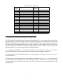
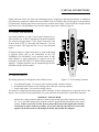
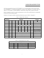
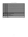
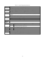
CIO-DAS802/16
User’s Manual
Revision 4
August, 2001
LIFETIME WARRANTY
Every hardware product manufactured by Measurement Computing Corp. is warranted against defects in materials or
workmanship for the life of the product, to the original purchaser. Any products found to be defective will be repaired or
replaced promptly.
LIFETIME HARSH ENVIRONMENT WARRANTYTM
Any Measurement Computing Corp. product which is damaged due to misuse may be replaced for only 50% of the current
price. I/O boards face some harsh environments, some harsher than the boards are designed to withstand. When that happens,
just return the board with an order for its replacement at only 50% of the list price. Measurement Computing Corp. does not
need to profit from your misfortune. By the way, we will honor this warranty for any other manufacture’s board that we have a
replacement for!
30 DAY MONEY-BACK GUARANTEE
Any Measurement Computing Corp. product may be returned within 30 days of purchase for a full refund of the price paid for
the product being returned. If you are not satisfied, or chose the wrong product by mistake, you do not have to keep it. Please
call for a RMA number first. No credits or returns accepted without a copy of the original invoice. Some software products
are subject to a repackaging fee.
These warranties are in lieu of all other warranties, expressed or implied, including any implied warranty of merchantability
or fitness for a particular application. The remedies provided herein are the buyer’s sole and exclusive remedies. Neither
Measurement Computing Corp., nor its employees shall be liable for any direct or indirect, special, incidental or
consequential damage arising from the use of its products, even if Measurement Computing Corp. has been notified in
advance of the possibility of such damages.
MEGA-FIFO, the CIO prefix to data acquisition board model numbers, the PCM prefix to data acquisition board model
numbers, PCM-DAS08, PCM-D24C3, PCM-DAC02, PCM-COM422, PCM-COM485, PCM-DMM, PCM-DAS16D/12,
PCM-DAS16S/12, PCM-DAS16D/16, PCM-DAS16S/16, PCI-DAS6402/16, Universal Library, InstaCal, Harsh
Environment Warranty and Measurement Computing Corp. are registered trademarks of Measurement Computing Corp.
IBM, PC, and PC/AT are trademarks of International Business Machines Corp. Windows is a trademark of Microsoft Corp.
All other trademarks are the property of their respective owners.
Information furnished by Measurement Computing Corp. is believed to be accurate and reliable. However, no responsibility is
assumed by Measurement Computing Corp. neither for its use; nor for any infringements of patents or other rights of third
parties, which may result from its use. No license is granted by implication or otherwise under any patent or copyrights of
Measurement Computing Corp.
All rights reserved. No part of this publication may be reproduced, stored in a retrieval system, or transmitted, in any form by
any means, electronic, mechanical, by photocopying, recording or otherwise without the prior written permission of
Measurement Computing Corp.
Notice
Measurement Computing Corp. does not authorize any Measurement Computing Corp. product for use in
life support systems and/or devices without the written approval of the President of Measurement
Computing Corp. Life support devices/systems are devices or systems which, a) are intended for surgical
implantation into the body, or b) support or sustain life and whose failure to perform can be reasonably
expected to result in injury. Measurement Computing Corp. products are not designed with the
components required, and are not subject to the testing required to ensure a level of reliability suitable for
the treatment and diagnosis of people.
© Copyright 2001, Measurement Computing Corp.
HM CIO-DAS802_16.lwp
Table of Contents
................
...........................................................................................
1: INSTALLATION
..................................................................... 1
1.1 SOFTWARE INSTALLATION . . . . . . . . . . . . . . . . . . . . . . . . . . . . . . . . . . . . . . . . . . . . . . . . . . . . . . . . . 1
1.2 INSTALLATION SWITCH SETTINGS . . . . . . . . . . . . . . . . . . . . . . . . . . . . . . . . . . . . . . . . . . . . . . . . . . 1
1.3 BASE ADDRESS . . . . . . . . . . . . . . . . . . . . . . . . . . . . . . . . . . . . . . . . . . . . . . . . . . . . . . . . . . . . . . . . . . . . 1
1.4 DIFFERENTIAL/SINGLE-ENDED INPUT SELECTION . . . . . . . . . . . . . . . . . . . . . . . . . . . . . . . . . . . . 2
1.5 INTERRUPT LEVEL SELECT . . . . . . . . . . . . . . . . . . . . . . . . . . . . . . . . . . . . . . . . . . . . . . . . . . . . . . . . . 3
1.7 WAIT STATE . . . . . . . . . . . . . . . . . . . . . . . . . . . . . . . . . . . . . . . . . . . . . . . . . . . . . . . . . . . . . . . . . . . . . . 4
1.8 INSTALLING THE BOARD IN THE COMPUTER
...................................... 4
1.9 CALIBRATION AND TEST
........................................................ 4
2: SIGNAL CONNECTION
.............................................................. 5
2.1 CONNECTOR DIAGRAM . . . . . . . . . . . . . . . . . . . . . . . . . . . . . . . . . . . . . . . . . . . . . . . . . . . . . . . . . . . . 5
2.1 ANALOG INPUTS . . . . . . . . . . . . . . . . . . . . . . . . . . . . . . . . . . . . . . . . . . . . . . . . . . . . . . . . . . . . . . . . . . 5
2.2 SINGLE-ENDED . . . . . . . . . . . . . . . . . . . . . . . . . . . . . . . . . . . . . . . . . . . . . . . . . . . . . . . . . . . . . . . . . . . . 6
2.3 FLOATING DIFFERENTIAL . . . . . . . . . . . . . . . . . . . . . . . . . . . . . . . . . . . . . . . . . . . . . . . . . . . . . . . . . . 6
2.4 FULLY DIFFERENTIAL . . . . . . . . . . . . . . . . . . . . . . . . . . . . . . . . . . . . . . . . . . . . . . . . . . . . . . . . . . . . . 6
2.5 DIGITAL OUTPUTS & INPUTS . . . . . . . . . . . . . . . . . . . . . . . . . . . . . . . . . . . . . . . . . . . . . . . . . . . . . . . 6
3: REGISTER ARCHITECTURE . . . . . . . . . . . . . . . . . . . . . . . . . . . . . . . . . . . . . . . . . . . . . . . . . . . . . . . . . . . 7
4: PACER/COUNTER/TIMER CIRCUIT . . . . . . . . . . . . . . . . . . . . . . . . . . . . . . . . . . . . . . . . . . . . . . . . . . . 11
5: SPECIFICATIONS
. . . . . . . . . . . . . . . . . . . . . . . . . . . . . . . . . . . . . . . . . . . . . . . . . . . . . . . . . . . . . . . . . . 12
This page is blank.
1: INSTALLATION
The CIO-DAS802/16 boards are an extension of the popular CIO-DAS08 architecture. The CIO-DAS802/16 has
a set of registers identical to the CIO-DAS08, and an additional set of registers for the extended features. Software written for the DAS08 will work without modification, but will not provide access to the extended features.
The connector is nearly identical to the CIO-DAS08, and more closely resembles the CIO-DAS08-PGA.
1.1 SOFTWARE INSTALLATION
Before you open your computer and install the board, install and run InstaCal, the installation, calibration and
test utility included with your board. InstaCal will guide you through switch and jumper settings for your board.
Detailed information regarding these settings can be found below. Refer to the Software Installation manual for
InstaCal installation instructions.
1.2 INSTALLATION SWITCH SETTINGS
There are two banks of switches and two jumpers to set on the CIO-DAS802/16 before installing your board into
your computer.
1. BASE ADDRESS SWITCH. A base address must be chosen and selected via switches.
2. INPUT SELECT SWITCHES. Analog inputs are differential or single ended. You may choose either on a
channel by channel basis. The set of DIP switches on the board, labeled S2, 0 through 7, correspond to the
channels 0 to 7 of the analog inputs.
3. INTERRUPT SELECT JUMPER. In order to take advantage of high speed transfers, you must provide the
board with an interrupt that is not used by other devices in your computer. Use the IR jumper to select an
interrupt level between 2 and 7 or to disable interrupts (X).
4. WAIT STATE JUMPER. A wait state jumper allows you to slow down a potentially too-fast computer bus,
but we have not seen the need for it yet. Set jumper WS1 to “ON” to enable wait states.
1.3 BASE ADDRESS
The base address of the CIO-DAS802/16 is set by switching a bank of DIP switches on the board. This bank of
switches is labeled ADDRESS and numbered 9 to 3. Refer to the Software Installation Manual for instructions
for using InstaCal as an aid in setting the base address switches.
Ignore the word ON and the numbers printed on the switch.
The switch works by adding up the weights of individual switches to make
a base address. A switch is active when down. In Figure 1-1, switches 9
and 8 are down, all others are up. Weights 200h and 100h are active,
totaling 300h base address.
Table 1-1 lists PC I/O assignments.
Figure 1-1. Base Address Switch
1
Table 1-1. PC I/O Assignments
HEX
RANGE
000-00F
020-021
040-043
060-063
060-064
070-071
080-08F
0A0-0A1
0A0-0AF
0C0-0DF
0F0-0FF
1F0-1FF
200-20F
210-21F
238-23B
23C-23F
270-27F
2B0-2BF
FUNCTION
8237 DMA #1
8259 PIC #1
8253 TIMER
8255 PPI (XT)
8742 CONTROLLER (AT)
CMOS RAM & NMI MASK (AT)
DMA PAGE REGISTERS
8259 PIC #2 (AT)
NMI MASK (XT)
8237 #2 (AT)
80287 NUMERIC CO-P (AT)
HARD DISK (AT)
GAME CONTROL
EXPANSION UNIT (XT)
BUS MOUSE
ALT BUS MOUSE
PARALLEL PRINTER
EGA
HEX
RANGE
2C0-2CF
2D0-2DF
2E0-2E7
2E8-2EF
2F8-2FF
300-30F
310-31F
320-32F
378-37F
380-38F
3A0-3AF
3B0-3BB
3BC-3BF
3C0-3CF
3D0-3DF
3E8-3EF
3F0-3F7
3F8-3FF
FUNCTION
EGA
EGA
GPIB (AT)
SERIAL PORT
SERIAL PORT
PROTOTYPE CARD
PROTOTTYPE CARD
HARD DISK (XT)
PARALLEL PRINTER
SDLC
SDLC
MDA
PARALLEL PRINTER
EGA
CGA
SERIAL PORT
FLOPPY DISK
SERIAL PORT
1.4 DIFFERENTIAL/SINGLE-ENDED INPUT SELECTION
The CIO-DAS802/16 has differential analog inputs. Differential inputs are 3-wire analog hookups consisting of a
signal high, signal low and chassis ground. The benefits of differential inputs are the ability to reject noise which
affects both signal high and low, and the ability to compensate for ground loops or potentials between signal low
and chassis ground. Although differential inputs are often preferable to single ended inputs, there are occasions
when the floating nature of a differential input can confound attempts to make a reading. In such cases, the CIODAS802/16 inputs are converted to single-ended or modified differential.
The CIO-EXP16 and CIO-EXP32 were designed to interface to a single-ended input. Failure to set the switches
to single-ended when an EXP is connected will result in floating, unstable readings from the EXP.
The analog inputs of the CIO-DAS802/16 may be set up as single ended or differential. There are two ways to
select between them.
The first method of selecting between the single ended and differential inputs is via a set of eight switches
located near the connector and labeled 0-7 in white lettering on the board. In the down, or off position, the input
associated with that switch is in differential mode. In the up, or on position the input associated with that switch
is single ended.
2
Figure 1-2. Differential-to-Single-Ended Switching
Figure 1-2 is a diagram of one analog input and the single-ended/differential switch. It shows the switch in the
Open position, so the input mode is differential.
The second method of converting the inputs to single ended is to install a SIP resistor pack at position RN2. This
package of 10K resistors provides a reference to ground for
each of the eight Low Input lines. This type of input
behaves like a single ended input in that there is a reference
to ground and floating sources may be measured, and it also
is able to reject a certain amount of noise.
Figure 1-3 shows an analog input line with the SIP resistor
installed.
Note that the SIP resistor is installed to all eight lines so
none of the analog inputs are fully differential after the SIP
is installed.
Figure 1-3. Differential-to-Single-Ended
If you intend to use an EXP board with the CIO-DAS802/16, do not install the SIP resistor but you should set the
SE/DI switch to ON for both the EXP channel and the CJC channel.
1.5 INTERRUPT LEVEL SELECT
The interrupt jumper need only be set if the software you are using requires it. The Universal Library and other
programs which take advantage of the REP-INSW high speed transfer capability
of the board require and interrupt. If you do set the interrupt jumper, please check
your PC's current configuration for interrupt conflicts.
There is a jumper block on the CIO-DAS802/16 located just above the PC bus
interface (gold pins). The factory default setting is that no interrupt level is set
(the jumper is in the 'X' position).
Figure 1-4. Interrupt Level Jumper
3
Refer to Table 1-2 for typical IRQ assignments.
Table 1-2. Hardware Interrupts
NAME
NMI
IRQ0
IRQ1
IRQ2
IRQ3
IRQ4
IRQ5
IRQ6
IRQ7
DESCRIPTION
PARITY
TIMER
KEYBOARD
RESERVED (XT)
INT 8-15 (AT)
COM OR SDLC
COM OR SDLC
HARD DISK (XT)
LPT (AT)
FLOPPY DISK
LPT
NAME
IRQ8
IRQ9
IRQ10
IRQ11
DESCRIPTION
REAL TIME CLOCK (AT)
RE-DIRECTED TO IRQ2 (AT)
UNASSIGNED
UNASSIGNED
IRQ12
IRQ13
IRQ14
UNASSIGNED
80287 NUMERIC CO-P
HARD DISK
IRQ15
UNASSIGNED
Note: IRQ8-15 are AT only
1.7 WAIT STATE
A wait state can be enabled on the CIO-DAS802/16 by selecting WAIT STATE ON at the jumper provided on
the board. Enabling the wait state causes the personal computer's bus transfer rate to slow down whenever the
CIO-DAS802/16 is written to or read from. The wait state jumper is provided in you have a computer has an I/O
bus transfer rate that is too fast for the CIO-DAS802/16. If your board were to fail sporadically in random ways,
try using it with the wait state ON.
1.8 INSTALLING THE BOARD IN THE COMPUTER
1. Turn the power off.
2. Remove the cover of your computer. Be careful not to dislodge any of the cables installed on the boards in
your computer as you slide the cover off.
3. Locate an empty expansion slot in your computer.
4. Insert and push the board firmly down into the expansion bus connector. If it is not seated fully it may fail to
work and could short circuit the PC bus power onto a PC bus signal. This could damage the motherboard in your
PC as well as the board.
1.9 CALIBRATION AND TEST
The CIO-DAS802/16 is supplied with InstaCal, software for calibration and test. If you have not done so, install
this software in order to test your board and, when necessary, calibrate it.
Every board is fully tested and calibrated before shipment. For normal environments, a calibration interval of 6
months to one year is recommended. If frequent variations in temperature or humidity are common, re-calibrate
at least once every three months. It takes less than 30 minutes to calibrate the CIO-DAS802/16.
4
2: SIGNAL CONNECTIONS
Signal connection can be one of the most challenging aspects of applying a data acquisition board. In addition to
just plain wrong connection, which is the most common cause of customer calls to tech support, is the possibility
of ground loops, floating signal sources and excessive common mode voltage. Please follow the examples shown
here and use care with grounding between the PC and the signal source. Refer to Figure 2-1.
2.1 CONNECTOR DIAGRAM
The analog connector is a male 37-pin, D-type connector accessible from the rear of the PC through the expansion backplate.
The connector accepts female 37-pin, D-type connectors, such
as those on the C73FF-2, 2 foot cable with connectors. The connector pin names Ch# High and Ch# Low are the differential
inputs.
If frequent changes to signal connections or signal conditioning
is required, please refer to the information on the CIOTERMINAL and CIO-MINI37 screw terminal boards. If additional channels or signal conditioning is required, refer to the
information on the CIO-EXP32, 32 channel analog multiplexer /
amplifier. Isolation amplifiers may be mounted using the ISORACK08 and 5B isolation modules.
2.1 ANALOG INPUTS
The analog inputs may be configured in three different ways:
Figure 2-1. 37-Pin Analog Connector
1. True differential inputs. For sources with a separate ground, common to the PC.
2. Pseudo-differential inputs used for floating sources has noise rejection capability.
3. Single ended inputs. Also used for floating sources.
The manner of configuring the analog inputs and the schematic of those configurations is explained earlier in the
manual. This section covers the implications of a given connection and shows how to make that connection
WARNING - PLEASE READ
Measure the voltage potential (difference) between the ground signal at the signal source and the
PC. Use a volt meter and place the red probe on the PC ground and the black probe on the signal
ground. If there is more the 10 volts, do not connect the board to this signal source because
you will not be able to make any reading. If it is more than 30 volts, DO NOT connect this
signal to the board because it will damage the board and possibly the computer.
5
2.2 SINGLE-ENDED
A single-ended input is two wires connected to the board; a channel high (CH# High) and a Low Level Ground
(LLGND). The LLGND signal must be the same ground the PC is on. The CH# High is the voltage signal
source. Single-ended mode is selected by closing a switch.
2.3 FLOATING DIFFERENTIAL
A floating differential input is two wires from the signal source and a 10K ground reference resistor installed at
the board input. The two signals from the signal source are Signal High (CH# High) and Signal Low (CH# Low).
The reference resistor is connected between the CH# Low and LLGND pins. This is done with the SIP resistor
pack
A floating differential hookup is useful when the signal source is floating with respect to ground, such as a battery.
WARNING: Check it with a voltmeter that the signal source really floating before risking the board and PC.
2.4 FULLY DIFFERENTIAL
A differential signal has three wires from the signal source. There is Signal High (CH# High), Signal Low (CH#
Low) and Signal Ground (LLGND).
A differential connection allows you to connect the board to a signal source with a ground that is different from
the PC ground, but less than 10V difference, and still make a true measurement of the signal between CH# High
and CH# Low.
EXAMPLE: A laboratory instrument with its own wall plug. There are sometimes voltage differences in wall
grounds between outlets.
2.5 DIGITAL OUTPUTS & INPUTS
All the digital inputs and outputs are TTL level. TTL is an electronics industry term, short for Transistor Transistor Logic, with describes a standard for digital signals which are either at TTL low or TTL high; levels which
are detected by all other TTL devices. For a listing of the TTL level specifications for these digital lines, please
see the specifications at the end of this manual.
There are four digital outputs and three digital inputs. The digital outputs are controlled by a register on the
board and are updated each time the register is written to. The digital inputs are buffered by a register on the
board and each time the register is read from, the current high/low state of the digital I/O lines is obtained. The
lines are pulled high so a logical one is read when no signal is connected to an input
The digital lines also are used to control external EXP boards (all four outputs) and to trigger and gate A/D conversions (Digital In 1).
6
3: REGISTER ARCHITECTURE
All of the programmable functions of the CIO-DAS802/16 are accessible through the control and data registers.
The CIO-DAS802/16 is controlled and monitored by writing to and reading from 16 consecutive 8-bit I/O
addresses. The first address, or BASE ADDRESS, is determined by setting a bank of switches on the board.
Register manipulation is best left to experienced programmers as most of the possible functions are implemented
in easy-to-use Universal Library routines.
Summaries of the registers and their read and write functions are given on Tables 3-1 through 3-6.
Table 3-1. Register Write Functions
Write
Functions
D7
Register
Data Bits
D6
D5
D4
D3
Function
D2
D1
D0
Base + 0
Start Conversion
Base + 1
Start Conversion
Special Function - (Depends on value of CS0,1)
Base + 2
CS1/0=0/0
OP4
OP3
OP2
OP1
INTE
MA2
MA1
MA0
Control Register 1
CS1/0=0/1
HCEN
NA
GTEN
EACS
IEOC
DTEN
CASC
ITE
Conversion Control
CS1/0=1/0
NA
NA
EC2
EC1
EC0
SC2
SC1
SC0
Scan Limits Register
CSE
CS1
CS0
ENHF
R3
R2
R1
R0
Range/Control Select
Base + 3
Base + 4
8254 C/T 0 Control Register
Base + 5
8254 C/T 1 Control Register
A/D Timer
Base + 6
8254 C/T 2 Control Register
Cascade Pre-scaler
Base + 7
8254 Counter/Timer Control Register
Register
Table 3-2. Control Register Select Coding
Control Register Selected
CS1
0
0
1
1
CS0
0
1
0
1
Write Function
Control Reg # 1
Conversion Control RegisScan Limits Reg
Not defined
7
Read Function
Status Register #2
Status Register #2
Status Register #2
ID Register
Table 3-3. Range (Gain) Select Codes
Range / (Gain)
Range (Gain) Select:
R2
R1
R0
0
0
0
0
0
1
0
1
0
0
1
1
1
0
0
1
0
1
1
1
0
1
1
1
CIO-DAS802/16
Bip: ±10V
(g=1)
Uni: 0 to 10V (g=1)
Bip: ±5V
(g=2)
Uni: 0 to 5V
(g=2)
Bip: ±2.5V (g=4)
Uni: 0 to 2.5V (g=4)
Bip: ±1.25V (g=8)
Uni: 0 to 1.25V (g=8)
Table 3-4. Register Read Functions
READ
Functions
Register
Base + 0
D7
AD7
D6
AD6
D5
AD5
Data Bits
D4
D3
AD4
AD3
D2
AD2
D1
AD1
D0
AD0
Low byte read
Base + 1
AD15
AD14
AD13
AD12
AD11
AD10
AD9
AD8
High byte read
Base + 2
EOC
IP3
IP2
IP1
IRQ
MA2
MA1
MA0
Status Register 1
Base + 3
EACS
MA2
MA1
MA0
FFOV
R2
R1
R0
Gain/Control Status
Base + 4
8254 C/T 0 Status Register
Base + 5
8254 C/T 1 Status Register
Base + 6
8254 C/T 2 Status Register
Base + 7
CS1/0=
0/0,0/1,1/0
CS1/0 = 1/1
Function
Function depends on value of CS0/1 bits in Base +3:
HCEN
GTEN
INTE
IEOC
DT
DTEN
CASC
ITE
Status Register 2
ID7
ID6
ID5
ID4
ID3
ID2
ID1
ID0
ID Reg (801=2,
802=3)
8
Table 3-5. Bit Definitions
AD 11:0
CASC*
CS1:0
CSE
DT*
DTEN*
EACS*
EC2:0*
ENHF*
EOC
FFOV*
GTEN*
HCEN
IEOC
INTE
IP3:1
ITE*
MA2:0
OP4:1
R3:0
SC2:0*
R
RW
W
W
R
RW
RW
W
W
R
R
RW
RW
RW
RW
R
RW
RW
W
RW
W
Analog data input (Read low byte first)
Cascade AD Pacing Mode Enable (include CT/2)
Register Selection (See Table 3.1)
Register Select Enable/Range Select Disable
State of Digital Trigger (1=Trigger occured)
External Digital Trigger Enable (Edge trig if GTEN=0)
Enable Auto channel-scan
Channel-scan end value
Enable Interrupt on FIFO Half Full (Req. IEOC=1, HCEN must =1 to enable FIFO)
End-of-conversion (1 = busy, 0 = ready)
FIFO Overflow (full) =1. 0 if HCEN =0.
Gate Enable (Req. DTEN to enable HW gate)
Hardware Convert Enable
Interrupt Source (1 = End of Convert, 0 = Ext)
Interrupt enable (0 = disable, 1 = enable)
Digital Input bits.
Internal Time Base (8254) Enable
Mux address bits
Digital Output bits.
AD Range bits (See Table 3.3)
Channel-scan start value.
* Asterisk indicates that HCEN is required (as a final step) to make this bit
functional.
9
Table 3-6. Special Programming Instructions
Register
Conv/Control
HCEN is used as a master enable for AD Pacing
Set HCEN last, by itself (i.e., write 80h), set the other bits first
Scan Limits
Ending channel (n) can be lower than starting channel (m) :
Select Start and End Channel before setting EACS
m,...,6,7,0,1,...,n,m...
ID
Only the 1st two bits are needed for software, the upper six are for compatibility with KMB
software
ID 1/0: 0/0= (DAS800 [KMB only], 0/1= reserved, 1/0= DAS801, 1/1= DAS802
Gain/Range
Range bits can be written only when bit 7 is 0
CS1/0 bits can be written only when bit 7 is 1
Not all of the CIO-DAS08 PGA gains are supported
Operating
Modes
Pacing
Normal
Cascade
CTR2 divides the 1 MHz time base; AD converts when CTR2 counts to zero
CTR1 decrements each time CTR2 counts to zero;
AD converts when CTR1 counts to zero
Triggering
Gating
Edge
Level
Requires DTEN=1, GTEN=0
"Gate", Requires DTEN=1, GTEN=0
Bit
INT/XCLK
External Interrupt and External (Pacer) Clock are mutually exclusive
External Interrupt is rising edge, External Pacer is falling edge
10
4: PACER/COUNTER/TIMER CIRCUIT
There is an 82C54 counter/timer on board which can be used to:
y
y
y
y
Pace analog conversions
Measure frequency
Count events
Precisely time intervals
The software to support the timer is in the Universal Library. The connections to the hardware are explained
here. For detailed information on the 82C54 registers, please refer to the Intel or AMD data sheet for this part if
you wish to program the 82C54 registers directly.
The 82C54 contains three counters, each 16 bits wide. Of the three counters, two are dedicated to the pacing of
analog to digital conversions. These two, CTR1 and CTR2, when not in use by the A/D are available for other
tasks but are limited to some extent by the wiring and access to I/O pins. The first counter, CTR0 is fully available for your use. Figure 4-1 is a simplified block diagram of the 82C54 and related logic functions..
+5VD C
ALL
10K
CTR 0 OU T
2
3
O UT 0
CLK 0
G AT E 0
G AT E 1
22
CTR 1 OU T
O UT 1
CLK 1
5
82C 54
4
G AT E 2
10 M HZ CRY STA L
O SCILLATO R
DIVID E BY
10
CLK 2
CTR 2
O UT
O UT 2
6
CASCADE
CO NTRO L
LO GIC
START CO NVERT
PACER
CO NTRO L
LOG IC
DIN 1/
TRIG
25
IN T IN PUT /
X CLK
24
Figure 4-1. Pacer/Counter/Timer Block Diagram
11
5: SPECIFICATIONS
Power consumption
+5V quiescent
Analog input section
A/D converter type
Resolution
Number of channels
Input ranges
Polarity
A/D pacing
A/D Trigger sources
Data transfer
Channel configuration
430 mA typical, 675 mA max
AD7805PB, Successive Approximation
16 bits
8
±10V, ±5V, ±2.5V, ±1.25V, 0 to 10V, 0 to 5V, 0 to 2.5V, 0 to 1.25V,
fully programmable
Unipolar/Bipolar software-selectable, 11 ms max switching delay
Programmable: internal counter or external source (IR Input / XCLK,
falling edge) or software polled
External hardware (Digital In 1 / Trig, rising edge)
Interrupt or software polled from 256 sample FIFO buffer
DMA
A/D conversion time
Throughput
Differential (or pseudo-differential with installation of a SIP resistor)
or single-ended, switch-selectable for each channel
None
10 µs (including signal acquisition time)
100 kHz
Accuracy
Differential Linearity error
Integral Linearity error
No missing codes (guaranteed)
±0.0015% of reading ±1.5 LSB
+1.5/−1 LSB max
±1.5 LSB max
16 bits
Gain drift (A/D specs)
Zero drift (A/D specs)
±10 ppm/°C
±5 ppm/°C
Common Mode Range
CMRR @ 60 Hz
Input leakage current (@ 25 deg C)
Input impedance
Absolute maximum input voltage
±10V
90 dB min
100 nA
10 Mohms
±35V
12
Counter section
Counter type
Configuration
82C54
3 down counters , 16 bit resolution
Counter 0 - independent user counter
Source: external, user connector (Counter 0 In)
Gate: external, user connector (Gate 0)
Output: user connector (Counter 0 Out)
Counter 1 - ADC Pacer Lower Divider or independent user counter
Source: user connector (Counter 1 In) and optionally, Counter Out,
selectable by software
Gate: programmable, disabled or user connector (Gate 1)
Output: user connector (Counter 1 Out) and optionally to A/D start
convert, software selectable
Counter 2 - ADC Pacer Upper Divider
Source: internal 1 MHz oscillator
Gate: programmable, disabled or user connector (Gate 2)
Output: user connector (Counter 2 Out) and optionally to Counter 1
input, software selectable
Clock input frequency
High pulse width (clock input)
Low pulse width (clock input)
Gate width high
Gate width low
Input low voltage
Input high voltage
Output low voltage
Output high voltage
10 MHz max
30 ns min
50 ns min
50 ns min
50 ns min
0.8V max
2.0V min
0.4V max
3.0V min
Digital I/O section
Digital type
Configuration
Input: FPGA
Output: 74LS08
Two ports, 3 input and 4 output
Input low voltage
Input high voltage
Output low voltage (IOL = 8 mA)
Output high voltage (OH = −0.4 mA)
Absolute maximum input voltage
0.8V max
2.0V min
0.25V typical, 0.4V max
3.4V typical, 2.7V min
−0.5V, +5.5V
Interrupts
Jumper selectable: levels 2, 3, 4, 5, 6, 7, or not connected
Positive edge triggered
Programmable
External (IR Input / XCLK), A/D End-of-conversion, A/D FIFOhalf-full
Interrupt enable
Interrupt sources
Environmental
Operating temperature range
Storage temperature range
Humidity
0 to 50°C
−20 to 70°C
0 to 90% non-condensing
13
For your notes.
14
EC Declaration of Conformity
We, Measurement Computing Corp., declare under sole responsibility that the product:
CIO-DAS802/16
Part Number
Description
to which this declaration relates, meets the essential requirements, is in conformity with, and CE marking has been applied
according to the relevant EC Directives listed below using the relevant section of the following EC standards and other
normative documents:
EU EMC Directive 89/336/EEC: Essential requirements relating to electromagnetic compatibility.
EU 55022 Class B: Limits and methods of measurements of radio interference characteristics of information technology
equipment.
EN 50082-1: EC generic immunity requirements.
IEC 801-2: Electrostatic discharge requirements for industrial process measurement and control equipment.
IEC 801-3: Radiated electromagnetic field requirements for industrial process measurements and control equipment.
IEC 801-4: Electrically fast transients for industrial process measurement and control equipment.
Carl Haapaoja, Director of Quality Assurance
Measurement Computing Corporation
16 Commerce Boulevard,
Middleboro, Massachusetts 02346
(508) 946-5100
Fax: (508) 946-9500
E-mail: [email protected]
www. measurementcomputing.com