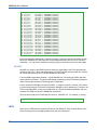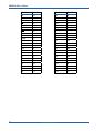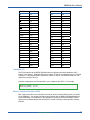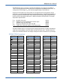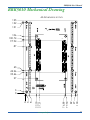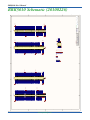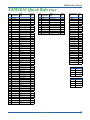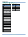
1
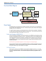
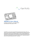
Opal Kelly
XEM5010 User’s Manual
A compact (85mm x 61mm) integration board featuring the Xilinx Virtex-5 FPGA and on-board DDR2
SDRAM, SSRAM, and SPI Flash.
The XEM5010 is a compact USB-based FPGA integration board featuring the Xilinx Virtex-5 FPGA, 256
MB 2x16-bit wide DDR2 SDRAM, 1Mx36 SyncSRAM, 32 Mb non-volatile flash, high-efficiency switching
power supplies, and two high-density 0.8-mm expansion connectors. The USB 2.0 interface provides
fast configuration downloads and FPGA-PC communication as well as easy access with our popular
FrontPanel software and developer’s API. An on-board low-jitter, LVDS clock oscillator provides a 100
MHz clock source to the FPGA.
Software, documentation, samples, and related materials are
Copyright © 2006-2014 Opal Kelly Incorporated.
Opal Kelly Incorporated
Portland, Oregon
http://www.opalkelly.com
All rights reserved. Unauthorized duplication, in whole or part, of this document by any means except for brief
excerpts in published reviews is prohibited without the express written permission of Opal Kelly Incorporated.
Opal Kelly, the Opal Kelly Logo, and FrontPanel are trademarks of Opal Kelly Incorporated.
Linux is a registered trademark of Linus Torvalds. Microsoft and Windows are both registered trademarks of
Microsoft Corporation. All other trademarks referenced herein are the property of their respective owners and no
trademark rights to the same are claimed.
Revision History:
Date
Description
20090721
Initial release.
20090730
Corrected JP2 pins JP2-9, 10, 11, 12.
20090909
Fix typo on pinout page 23. (JP2 relabeled to JP3)
20091105
Updated documentation to include VDC input voltage range and proper location of +3.3v and
+1.0v outputs on JP2/JP3.
20091227
Added BRK5010 schematic and mechanical drawing.
20100226
Added BRK5010 errata.
20101101
Added example heatsink part number.
20101104
Added note about on-board termination for the LVDS oscillator.
20110926
Fixed SSRAM pin list.
20140331
Added remark about the Pins reference.
20140812
Fixed typo in I/O voltages section. Can set voltage on six banks (not four).
Contents
Introducing the XEM5010 . . . . . . . . . . . . . . . . . . . . . . . 5
PCB Footprint. . . . . . . . . . . . . . . . . . . . . . . . . . . . . . . . . . . . . 5
Functional Block Diagram. . . . . . . . . . . . . . . . . . . . . . . . . . . . 6
Power Supply. . . . . . . . . . . . . . . . . . . . . . . . . . . . . . . . . . . . . 6
Supply Heat Dissipation (IMPORTANT!!). . . . . . . . . . . . . 6
DC Power Connector. . . . . . . . . . . . . . . . . . . . . . . . . . . . 6
VBATT . . . . . . . . . . . . . . . . . . . . . . . . . . . . . . . . . . . . . . . 7
Supply Currents. . . . . . . . . . . . . . . . . . . . . . . . . . . . . . . . 7
USB Bus Power. . . . . . . . . . . . . . . . . . . . . . . . . . . . . . . . 7
USB 2.0 Interface. . . . . . . . . . . . . . . . . . . . . . . . . . . . . . . . . . 7
On-board Peripherals. . . . . . . . . . . . . . . . . . . . . . . . . . . . . . . 7
Clock Oscillator . . . . . . . . . . . . . . . . . . . . . . . . . . . . . . . . 7
Serial EEPROM. . . . . . . . . . . . . . . . . . . . . . . . . . . . . . . . 7
256-MByte Synchronous DDR2 DRAM (2x 128-MByte). 8
36-Mb Word-Wide Synchronous SRAM . . . . . . . . . . . . . 8
32-Mb SPI Serial Flash . . . . . . . . . . . . . . . . . . . . . . . . . . 8
LEDs and External LED Connections . . . . . . . . . . . . . . . 8
Expansion Connectors. . . . . . . . . . . . . . . . . . . . . . . . . . . . . . 8
FrontPanel Support. . . . . . . . . . . . . . . . . . . . . . . . . . . . . . . . . 8
Programmer’s Interface. . . . . . . . . . . . . . . . . . . . . . . . . . 8
Applying the XEM5010 . . . . . . . . . . . . . . . . . . . . . . . . . 11
Host Interface. . . . . . . . . . . . . . . . . . . . . . . . . . . . . . . . . . . . . 11
MUXSEL. . . . . . . . . . . . . . . . . . . . . . . . . . . . . . . . . . . . . . 12
LEDs. . . . . . . . . . . . . . . . . . . . . . . . . . . . . . . . . . . . . . . . . . . . 12
Clock Oscillator Connections. . . . . . . . . . . . . . . . . . . . . . . . . 13
JTAG. . . . . . . . . . . . . . . . . . . . . . . . . . . . . . . . . . . . . . . . . . . . 13
SPI Flash Connections. . . . . . . . . . . . . . . . . . . . . . . . . . . . . . 13
FPGA Configuration via SPI Flash . . . . . . . . . . . . . . . . . 13
DDR2 SDRAM. . . . . . . . . . . . . . . . . . . . . . . . . . . . . . . . . . . . 13
FPGA Connections. . . . . . . . . . . . . . . . . . . . . . . . . . . . . . 13
Cascaded DCI . . . . . . . . . . . . . . . . . . . . . . . . . . . . . . . . . 15
Memory Interface Generator (MIG). . . . . . . . . . . . . . . . . 15
MIG Settings. . . . . . . . . . . . . . . . . . . . . . . . . . . . . . . . . . . 16
MIG Pin Selection. . . . . . . . . . . . . . . . . . . . . . . . . . . . . . . 16
Synchronous SRAM. . . . . . . . . . . . . . . . . . . . . . . . . . . . . . . . 16
High-Performance Operation. . . . . . . . . . . . . . . . . . . . . . 16
SSRAM / FPGA Connections . . . . . . . . . . . . . . . . . . . . . 17
Expansion Connectors. . . . . . . . . . . . . . . . . . . . . . . . . . . . . . 18
IMPORTANT NOTE: 3.3v I/O Operation. . . . . . . . . . . . . 18
JP2. . . . . . . . . . . . . . . . . . . . . . . . . . . . . . . . . . . . . . . . . . 18
JP3. . . . . . . . . . . . . . . . . . . . . . . . . . . . . . . . . . . . . . . . . . 18
Setting I/O Voltages. . . . . . . . . . . . . . . . . . . . . . . . . . . . . 18
Considerations for Differential Signals. . . . . . . . . . . . . . . 19
BRK5010 Breakout Board. . . . . . . . . . . . . . . . . . . . . . . . . . . . 19
Errata: Datecode 20091013. . . . . . . . . . . . . . . . . . . . . . . 20
Errata: Datecode 20091013 and 20091209. . . . . . . . . . . 20
XEM5010 User’s Manual
XEM5010 Mechanical Drawing. . . . . . . . . . . . . . . . . . . 22
BRK5010 Mechanical Drawing . . . . . . . . . . . . . . . . . . . 23
BRK5010 Schematic (20100226). . . . . . . . . . . . . . . . . . 24
XEM5010 Quick Reference. . . . . . . . . . . . . . . . . . . . . . 25
XEM5010 Quick Reference. . . . . . . . . . . . . . . . . . . . . . 26
XEM5010 Quick Reference. . . . . . . . . . . . . . . . . . . . . . 27
XEM5010 Quick Reference. . . . . . . . . . . . . . . . . . . . . . 28
4
www.opalkelly.com
XEM3050 User’s Manual
Introducing the XEM5010
The XEM5010 is a compact (85mm x 61mm, 3.35” x 2.40”) FPGA board featuring the Xilinx
Virtex-5 FPGA. Designed as a full-featured integration system, the XEM5010 provides access
to 200 I/O pins on its 676-pin Virtex-5 device and has 256-MByte of DDR2 SDRAM, 36-Mb of
SSRAM, and 4-MByte of Flash memory available to the FPGA.
PCB Footprint
A mechanical drawing of the XEM5010 is shown at the end of this manual. The PCB is 85mm
x 61mm with four mounting holes spaced as shown in the figure. These mounting holes are
electrically isolated from all signals on the XEM5010. The two connectors (USB and DC power)
overhang the PCB by approximately 4mm in order to accomodate mounting within an enclosure.
The XEM5010 has two high-density 120-pin connectors on the bottom side which provide access
to many FPGA pins, power, JTAG, and the microcontroller’s I2C interface.
www.opalkelly.com
5
XEM5010 User’s Manual
Functional Block Diagram
100 MHz
LVDS OSC
USB
USB Micro
(CY68013A)
Host Interface
Bus
2x DDR2-667
(64Mx16)
Virtex-5 FPGA
(XC5VLX50-1FGG676)
100 I/O
JTAG
80 I/O
20 GCLK
SSRAM
(1Mx36)
Flash
(32Mb)
4 LEDs
XBUS (JP2)
YBUS (JP3)
Power Supply
The XEM5010 has four high-efficiency switching regulators to provide clean, well-regulated power to the FPGA and peripherals on the board. These are Enpirion power modules and configured
to supply 3.3v, 2.5v, 1.8v, and 1.0v.
P1 is the DC power connector on the board and sources +VDC to all four regulators. Alternatively, +VDC can be provided through the expansion connector (JP3). +VDC must be sourced from a
well-regulated power supply in the range of +4.5v to +5.5v.
Supply Heat Dissipation (IMPORTANT!!)
Due to the limited area available on the small form-factor of the XEM5010 and the density of logic
provided, heat dissipation should be a concern. This depends entirely on the end application and
cannot be predicted in advance by Opal Kelly. Heat sinks may be required on any of the devices
on the XEM5010. Of primary focus should be the FPGA (U12). Although the switching supplies
are high-efficiency, they are very compact and consume a small amount of PCB area for the current they can provide.
The FPGA will require additional passive or active cooling for even simple designs.
One such passive heatsink would be the INM27002-12PCU/2.6 available from Radian (www.radianheatinks.com). The blue clip version (BU+T710) fits the Virtex-5 on the XEM5010. Of course,
this specific heatsink may not be suitable for all designs.
DC Power Connector
The DC power connector on the XEM5010 is part number PJ-102AH from CUI, Inc. It is a standard 2.1mm / 5.5mm power jack. The outer ring is attached to DGND. The center pin is attached
to +VDC on expansion connector JP3 as well as the inputs to the switching regulators on the
XEM5010.
6
www.opalkelly.com
XEM5010 User’s Manual
VBATT
+VBATT is connected to the JP3 expansion connector and can be powered by a daughterboard
to the FPGA. This voltage is used to maintain a small memory on the FPGA to support bitstream
encryption. Please see the Xilinx Virtex-5 documentation for details.
Supply Currents
The on-board regulators provide the following supplies and respective current:
•
•
•
•
+3.3v @ 1.0A - USB microcontroller, clock oscillator, and default FPGA I/O.
+2.5v @ 2.0A - FPGA VCCAUX
+1.8v @ 1.0A - DDR2 SDRAM and SSRAM
+1.0v @ 6.0A - FPGA VCCINT
+3.3v is available on JP2 and +1.0v is available on JP3. Designers should note the current limitations before deciding to use these supplies.
USB Bus Power
The USB 2.0 specification allows for up to 2.5 W (500mA at 5v) to be provided to external peripherals over the USB cable. Due to the potentially high power requirements of the XEM5010,
USB power has not been connected. However, the XEM firmware reports to the USB hub as a
500-mA device.
USB 2.0 Interface
The XEM5010 uses a Cypress CY7C68013A FX2LP USB microcontroller to make the XEM a
USB 2.0 peripheral. As a USB peripheral, the XEM is instantly recognized as a plug and play
peripheral on millions of PCs. More importantly, FPGA downloads to the XEM happen blazingly
fast, virtual instruments under FrontPanel update quickly, and data transfers are much faster than
the parallel port interfaces common on many FPGA experimentation boards.
On-board Peripherals
The XEM5010 is designed to compactly support a large number of applications with a small number of on-board peripherals. These peripherals are listed below.
Clock Oscillator
The clock oscillator produces a 100 MHz (±50ppm) LVDS signal with 45/55% symmetry and 0.5ps typical phase jitter (1.0-ps RMS max) measured from 12 kHz - 80 MHz.
Serial EEPROM
A small serial EEPROM is attached to the USB microcontroller on the XEM5010, but not directly
available to the FPGA. The EEPROM is used to store boot code for the microcontroller as well
as a device identifier string.
The device identifier string may be changed at any time using FrontPanel. The string serves only
a cosmetic purpose and is used when multiple XEM devices are attached to the same computer
so you may select the proper active device.
www.opalkelly.com
7
XEM5010 User’s Manual
256-MByte Synchronous DDR2 DRAM (2x 128-MByte)
The XEM also includes two 128-MByte DDR2 SDRAM with fully independent 16-bit word-wide
interfaces to the FPGA. This SDRAMs are attached exclusively to the FPGA and do not share
any pins with the expansion connector. The maximum clock rate of the SDRAM is 266 MHz.
None of the pins (control, address, or data) are shared between the two SDRAM busses.
The SDRAM is a Micron MT47H64M16HR-3:G (or compatible).
36-Mb Word-Wide Synchronous SRAM
One synchronous SRAM (1M x 36 configuration) is included with dedicated address, data, and
control lines routed to the FPGA. The SSRAM is a GSI Technology GS8322Z36GB-200V (or
equivalent).
32-Mb SPI Serial Flash
One Numonyx M25P32 (or equivalent) SPI serial flash is connected to the FPGA for non-volatile
storage.
LEDs and External LED Connections
Four on-board LEDs are provided for general use. In addition, a 5-pin expansion connector (JP4)
allows the connection of a external LEDs. Four pins of this connector are wired to FPGA pins via
series 330-Ω resistors.
Expansion Connectors
Two high-density, 120-pin expansion connectors are available on the bottom-side of the
XEM5010 PCB. These expansion connectors provide user access to several power rails on
the XEM5010, several FPGA clock inputs, the JTAG chain, and 200 non-shared I/O pins on the
FPGA.
The connectors on the XEM5010 are Samtec part number: QSE-060-01-F-D-A. The table below
lists the appropriate Samtec mating connectors along with the total mated height.
Samtec Part Number
Mated Height
QTE-060-01-F-D-A
5.00mm (0.198”)
QTE-060-02-F-D-A
8.00mm (0.316”)
FrontPanel Support
The XEM5010 is fully supported by Opal Kelly’s FrontPanel software. FrontPanel augments
the limited peripheral support with a host of PC-based virtual instruments such as LEDs, hex
displays, pushbuttons, toggle buttons, and so on. Essentially, this makes your PC a reconfigurable I/O board and adds enormous value to the XEM5010 as an experimentation or prototyping
system.
Programmer’s Interface
In addition to complete support within FrontPanel, the XEM5010 is also fully supported by the
FrontPanel programmer’s interface (API), a powerful C++ class library available to Windows and
Linux programmers allowing you to easily interface your own software to the XEM.
8
www.opalkelly.com
XEM5010 User’s Manual
In addition to the C++ library, wrappers have been written for C#, Java, Python, and Ruby making
the API available under those languages as well. Sample wrappers are also provided for Matlab
and LabVIEW.
Complete documentation and several sample programs are installed with FrontPanel.
www.opalkelly.com
9
XEM5010 User’s Manual
10
www.opalkelly.com
XEM3050 User’s Manual
Applying the XEM5010
Host Interface
There are 26 pins that connect the on-board USB microcontroller to the FPGA. These pins comprise the host interface on the FPGA and are used for configuration downloads. After configuration, these pins are used to allow FrontPanel communication with the FPGA.
If the FrontPanel okHost module is instantiated in your design, you must map the interface pins to
specific pin locations using Xilinx LOC constraints. This may be done using the Xilinx constraints
editor or specifying the constraints manually in a text file. An example is shown below:
Xilinx constraints for okHost pin mappings:
www.opalkelly.com
11
XEM5010 User’s Manual
NET
NET
NET
NET
NET
NET
NET
NET
NET
NET
NET
NET
NET
NET
NET
NET
NET
NET
NET
NET
NET
NET
NET
NET
NET
NET
NET
“hi_in<0>”
“hi_in<1>”
“hi_in<2>”
“hi_in<3>”
“hi_in<4>”
“hi_in<5>”
“hi_in<6>”
“hi_in<7>”
“hi_out<0>”
“hi_out<1>”
“hi_inout<0>”
“hi_inout<1>”
“hi_inout<2>”
“hi_inout<3>”
“hi_inout<4>”
“hi_inout<5>”
“hi_inout<6>”
“hi_inout<7>”
“hi_inout<8>”
“hi_inout<9>”
“hi_inout<10>”
“hi_inout<11>”
“hi_inout<12>”
“hi_inout<13>”
“hi_inout<14>”
“hi_inout<15>”
“hi_muxsel”
LOC=”AD13”
LOC=”AD15”
LOC=”AD14”
LOC=”AB12”
LOC=”Y8”
LOC=”AA8”
LOC=”AA17”
LOC=”AB17”
LOC=”AC14”
LOC=”AC11”
LOC=”AD18”
LOC=”AC18”
LOC=”AB10”
LOC=”AB9”
LOC=”AC17”
LOC=”AC16”
LOC=”AC8”
LOC=”AC9”
LOC=”Y12”
LOC=”Y13”
LOC=”AA15”
LOC=”AB14”
LOC=”AA12”
LOC=”AB11”
LOC=”AA13”
LOC=”AA14”
LOC=”AB15”
|
|
|
|
|
|
|
|
|
|
|
|
|
|
|
|
|
|
|
|
|
|
|
|
|
|
|
IOSTANDARD=”LVCMOS33”;
IOSTANDARD=”LVCMOS33”;
IOSTANDARD=”LVCMOS33”;
IOSTANDARD=”LVCMOS33”;
IOSTANDARD=”LVCMOS33”;
IOSTANDARD=”LVCMOS33”;
IOSTANDARD=”LVCMOS33”;
IOSTANDARD=”LVCMOS33”;
IOSTANDARD=”LVCMOS33”;
IOSTANDARD=”LVCMOS33”;
IOSTANDARD=”LVCMOS33”;
IOSTANDARD=”LVCMOS33”;
IOSTANDARD=”LVCMOS33”;
IOSTANDARD=”LVCMOS33”;
IOSTANDARD=”LVCMOS33”;
IOSTANDARD=”LVCMOS33”;
IOSTANDARD=”LVCMOS33”;
IOSTANDARD=”LVCMOS33”;
IOSTANDARD=”LVCMOS33”;
IOSTANDARD=”LVCMOS33”;
IOSTANDARD=”LVCMOS33”;
IOSTANDARD=”LVCMOS33”;
IOSTANDARD=”LVCMOS33”;
IOSTANDARD=”LVCMOS33”;
IOSTANDARD=”LVCMOS33”;
IOSTANDARD=”LVCMOS33”;
IOSTANDARD=”LVCMOS33”;
Each of the samples installed with FrontPanel includes a copy of a template constraints file that
lists all the XEM5010 pins and maps them to the appropriate FPGA pins using LOC (location)
constraints. You can use this template to quickly get the pin locations correct on a new design.
MUXSEL
MUXSEL is a signal on the XEM5010 which selects the signal path to the FPGA programming
signals D0 and CCLK. When low (deasserted), the FPGA and USB microcontroller are connected. When high (asserted), the FPGA and PROM are connected.
In normal USB-programmed operation, J1 pulls MUXSEL low, connecting the FPGA and USB
microcontroller at all times. This allows USB-based programming of the FPGA and subsequent
USB communication with the FPGA design after configuration.
In order to allow the PROM to configure the FPGA, J1 must be removed. However, if the USB is
to communicate with the FPGA post-configuration, MUXSEL must be deasserted. Therefore, the
FPGA outputs MUXSEL so that, post-configuration, the FPGA can deassert MUXSEL and communicate over USB even after the PROM has configured it.
The end result is that your FPGA design should tie HI_MUXSEL to 0. For example, in Verilog:
assign hi_muxsel = 1’b0;
LEDs
There are four LEDs and four external LED pins on the XEM5010. Each is wired directly to the
FPGA according to the pin mapping tables at the end of this document.
12
www.opalkelly.com
XEM5010 User’s Manual
The LED anodes are connected to a pull-up resistor to +3.3VDD and the cathodes wired directly
to the FPGA. To turn ON an LED, the FPGA pin should be brought low. To turn OFF an LED,
the FPGA pin should be brought high.
The external LED connector is wired a bit differently. JP4-1 is attached to +3.3VDD. JP4-2
through JP4-5 are each attached through a 330-Ω resistor to an FPGA pin. Externally, you
should connect the four LED anodes to JP4-1 (+3.3VDD). The four cathode should be attached
to the other pins on JP4.
Clock Oscillator Connections
The LVDS clock oscillator produces a 100 MHz LVDS signal which is presented on FPGA pins
AD8 and AC7. These are L4P_GC_4 and L4N_GC4 inputs, respectively. An on-board 100-ohm
termination resistor is present.
JTAG
On the XEM5010, the FPGA is the only device on the JTAG chain. The JTAG pins connecting to
the FPGA are available on the expansion connector JP2 so that you can attach a suitable JTAG
chain or programmer on your boart.
SPI Flash Connections
The on-board SPI flash device is attached to the FPGA according to the following table.
Flash Pin
Signal
CLK
AA18
CS
AA10
DOUT
Y18
DIN
AA9
FPGA Configuration via SPI Flash
The Virtex-5 on the XEM5010 may be configured by USB or SPI Flash. When using USB, the
FPGA may be configured at any time. When booting by SPI Flash, configuration takes place at
power-on. To boot to the configuration file loaded into the SPI Flash, remove the jumper at J1.
To load the SPI Flash with your configuration data, we have provided a sample (FlashLoader)
which is located in the Samples directory of your installation. This is a simple command-line
utility that can be used to transfer a configuration bitfile to SPI Flash. The source code to the
software is included so you can include this utility in your own application, if required.
DDR2 SDRAM
FPGA Connections
The DDR2 SDRAMs are connected exclusively to the 1.8v I/O on Banks 11, 12, 15, and 16 of the
FPGA. The tables below list these connections. DDR2A is U15 on the PCB. DDR2B is U14.
www.opalkelly.com
13
XEM5010 User’s Manual
DDR2A Pin
FPGA Pin
DDR2A Pin
FPGA Pin
CK
D5
A9
B4
CK
D6
A10
C4
CKE
H6
A11
C7
CS
F4
A12
C6
RAS
G6
BA0
E5
CAS
G7
BA1
E6
WE
F5
BA2
F7
LDQS
D8
D0
D11
LDQS
C8
D1
D10
UDQS
B7
D2
C11
UDQS
A7
D3
C12
LDM
C13
D4
B12
UDM
A9
D5
A13
ODT
J6
D6
A12
A0
E7
D7
C9
A1
B2
D8
B9
A2
B1
D9
B10
A3
C1
D10
B11
A4
D1
D11
A10
A5
A3
D12
A8
A6
A2
D13
B5
A7
C3
D14
B6
C2
D15
D3
A8
14
www.opalkelly.com
XEM5010 User’s Manual
DDR2B Pin
FPGA Pin
DDR2B Pin
FPGA Pin
CK
D21
A9
C23
CK
D20
A10
B24
CKE
H21
A11
B21
CS
F23
A12
C21
RAS
E22
BA0
E20
CAS
E23
BA1
E21
WE
F22
BA2
F20
LDQS
A20
D0
C14
LDQS
B20
D1
B14
UDQS
C19
D2
A14
UDQS
D19
D3
A15
LDM
B15
D4
B16
UDM
B19
D5
D16
ODT
G21
D6
C16
A0
G20
D7
D18
A1
D25
D8
B17
A2
D26
D9
A17
A3
C26
D10
A18
A4
B26
D11
A19
A5
A25
D12
C18
A6
B25
D13
B22
A7
C24
D14
A22
D24
D15
A23
A8
Cascaded DCI
The FPGA interface to the DDR2 SDRAM utilizes the digitally-controlled impedance (DCI)
feature of the Virtex-5. VRN and VRP pads on banks 15 and 16 are attached through 1% 49.9Ω
resistors to +1.8VDD and DGND, respectively. Banks 11 and 12 use references that are “cascaded” from banks 15 and 16.
Cascade configuration must be specified in your constraints file (.UCF). For example:
CONFIG DCI_CASCADE = “16 12”;
CONFIG DCI_CASCADE = “15 11”;
Memory Interface Generator (MIG)
MIG is part of the Xilinx Core Generator and can be used to create a DDR2 memory controller
for the XEM5010. You should read and become familiar with the DDR2 SDRAM datasheet as
well as MIG and the core datasheet. Although MIG can save a tremendous amount of development time, understanding all this information is critical to building a working DDR2 memory
interface.
www.opalkelly.com
15
XEM5010 User’s Manual
MIG Settings
The following are the settings used to generate the MIG core for our RAMTester sample using
Xilinx Core Generator. These settings were used with ISE 10.2 and MIG 2.3. Note that settings
may be slightly different for different versions of ISE or MIG.
Frequency
266 MHz
Memory Type
Component
Memory Part
MT47H64M16XX-3 (1Gb, x16)
Data Width16
Data Mask
Checked
Burst Length
4(010)
Burst Type
Sequential(0)
CAS Latency
4(100)
Output drive strength
Reducedstrength(1)
RTT(nominal)
75ohms(01)
Additive latency(AL)
0(000)
Use DCM
Your option
DCI for DQ/DQS
CHECKED
DCI for address/control
CHECKED
Class for address/control
Class II
Debug signals
Your option
Limit to 2 bytes per bank
No
System clockDifferential
[default]
[default]
[default]
[default]
[default]
MIG Pin Selection
To help MIG select the proper pins for the constraints (UCF), you can direct it to reserve nonDDR2 banks and tell it where to map controllers for the others. The selection process is:
● Reserve banks 1, 2, 3, 13, 14, 17, 18, 21. MIG will not use these.
● For controller C0, check all in banks 4, 12, 16. Uncheck all others.
● For controller C1, check all in banks 4, 11, 15. Uncheck all others.
Synchronous SRAM
The SSRAM has a full 36-bit wide data bus (4 bytes + 4 parity pits). The CLK pin is attached
directly to the FPGA with the intent that the FPGA provide a synchronous clock in the so-called
“source synchronous” manner. This helps align clock and data between the FPGA and SSRAM.
The redundant chip enable pins of the SSRAM have been tied to enable, as appropriate. E2
is tied to +1.8VDD and E3 is tied to DGND. ZQ has been left as a no-connect. LBO is tied to
DGND, enabling linear byte order operation. Finally, all four byte enables (BA, BB, BC, and BD)
are tied to DGND.
High-Performance Operation
The SSRAM can achieve operation to 200 MHz, but requires careful consideration of all FPGA
timing parameters. We provide the following as suggestions based on our development of test
code, but recommend a thorough timing analysis to achieve high-performance, reliable operation. A good understanding of the SSRAM and FPGA timing datasheets is critical to this analysis.
16
www.opalkelly.com
XEM5010 User’s Manual
The SSRAM has a 0.5-ns hold time. By setting the SSRAM_CLK output from the FPGA to
“FAST”, this can advance the timing of the CLK in comparison to the address/control lines. According to the FPGA timings (TIOOP), this achieves approximately 0.6-ns hold time.
Delays from FPGA pads to the internal fabric can be significant and cause problems at high
clock rates. You must consider all delays when determining timing. The following illustrates the
timings considered for SSRAM reads. Note that parts will differ depending on manufacturing
process corners and operating techniques. Adaptive techniques using the IDELAY elements
help achieve optimal results.
TOCKQ OLOGIC CLK-to-OQ
0.62 ns
TIOOP Delay from O pin to the IOB pad for CLOCK output
1.93 ns
TKQ
SSRAM clock to Q (read timing)
5.00 ns
TIOPI
Delay from IOB pad to the I pin of the IOB
0.89 ns
TIDOCK ILOGIC D pin setup with respect to CLK without delay
0.39 ns
Total
8.83 ns
This table indicates that for clock frequencies exceeding approximately 113 MHz, SSRAM data
reads may not be available to the FPGA fabric until the next clock cycle. Therefore, there is a
single-cycle read delay inherent in the design routing that must be accounted for in your design.
SSRAM / FPGA Connections
SSRAM Pin
FPGA Pin
SSRAM Pin
FPGA Pin
SSRAM Pin
FPGA Pin
CLK
R22
A14
R23
D14
N22
CKE
L4
A15
J23
D15
L22
WE
J21
A16
N23
DP2
L19
CE1
M22
A17
L23
D16
H9
OE
K22
A18
K23
D17
G11
ADV/LD
J5
A19
H23
D18
G10
ZZ
K5
A20
P23
D19
H11
FT
M6
D0
R7
D20
G12
A0
L5
D1
R5
D21
H12
A1
M5
D2
P4
D22
F13
A2
M4
D3
R6
D23
H13
A3
L3
D4
P6
DP3
G9
A4
J4
D5
N6
D24
G14
A5
H4
D6
P5
D25
H14
A6
G4
D7
M7
D26
G15
A7
P3
DP1
N7
D27
F15
A8
N4
D8
M19
D28
H17
A9
T3
D9
L20
D29
G17
A10
R3
D10
M21
D30
G16
A11
H19
D11
P20
D31
G19
A12
K20
D12
N21
DP4
H18
A13
P19
D13
P21
www.opalkelly.com
17
XEM5010 User’s Manual
Expansion Connectors
Opal Kelly Pins is an interactive online reference for the expansion connectors on all Opal Kelly
FPGA integration modules. It provides additional information on pin capabilities, pin characteristics, and PCB routing. Additionally, Pins provides a tool for generating constraint files for place
and route tools. Pins can be found at the URL below.
http://www.opalkelly.com/pins
IMPORTANT NOTE: 3.3v I/O Operation
As process technology shrinks, I/O voltages tend lower. The Xilinx Virtex-5 FPGA is no exception and has limited 3.3v I/O operation. Before using the XEM5010 to interface to any 3.3v design, please review the Xilinx Virtex-5 FPGA User Guide, Chapter 6: 3.3V I/O Design Guidelines.
JP2
JP2 is a 120-pin high-density connector providing access to FPGA Banks 13, 17, and 21.
Pin mappings for JP2 are listed at the end of this document in the “Quick Reference” section. For
each JP2 pin, the corresponding board connection is listed. For pins connected to the FPGA,
the corresponding FPGA pin number is also shown. Finally, for pins routed to differential pair I/
Os on the FPGA, the FPGA signal names and routed track lengths have been provided to help
you equalize lengths on differential pairs.
JP3
JP3 is a 120-pin high-density connector providing access to FPGA Banks 14, 18, and 3. Bank
3 is primarily a clock-input bank providing up to 10 differential clock inputs or 20 single-ended
inputs.
Pin mappings for JP3 are listed at the end of this document in the “Quick Reference” section. For
each JP3 pin, the corresponding board connection is listed. For pins connected to the FPGA,
the corresponding FPGA pin number is also shown. Finally, for pins routed to differential pair I/
Os on the FPGA, the FPGA signal names and routed track lengths have been provided to help
you equalize lengths on differential pairs.
Setting I/O Voltages
The Virtex-5 FPGA allows users to set I/O bank voltages in order to support several different I/O
signalling standards. This functionality is supported by the XEM5010 by allowing the user to connect independent supplies to the FPGA VCCO pins on six of the FPGA banks.
By default, ferrite beads have been installed which attach each VCCO bank to the +3.3VDD
supply. If you intend to supply power to a particular I/O bank, you MUST remove the appropriate
ferrite beads. Power can then be supplied through the expansion connectors.
The table below lists details for user-supplied I/O bank voltages.
18
I/O Bank
Expansion Pin
FPGA Pins
Ferrite Bead
3
JP3-2, JP3-4
E14, D17
FB5
www.opalkelly.com
XEM5010 User’s Manual
I/O Bank
Expansion Pin
FPGA Pins
Ferrite Bead
13
JP2-1, JP2-3
N20, M23, R24
FB1
14
JP3-41, JP3-43
W2, R4, V5
FB2
17
JP2-42, JP2-44
T21, W22, V25
FB3
18
JP3-85, JP3-87
AB3, AA6, AD7
FB4
21
JP2-86, JP2-88
AC20, AB23, AE24
FB6
Considerations for Differential Signals
The XEM5010 PCB layout and routing has been designed with several applications in mind,
including applications requiring the use of differential (LVDS) pairs. Please refer to the Xilinx
Virtex-5 datasheet for details on using differential I/O standards with the Virtex-5 FPGA.
FPGA I/O Bank Voltages
In order to use differential I/O standards with the Virtex-5, you must set the VCCO voltages for
the appropriate banks to 2.5v according to the Xilinx Virtex-5 datasheet. Please see the section
above entitled “Setting I/O Voltages” for details.
Characteristic Impedance
The characteristic impedance of all routes from the FPGA to the expansion connector is 50-Ω.
Differential Pair Lengths
In many cases, it is desirable that the route lengths of a differential pair be matched within some
specification. Care has been taken to route differential pairs on the FPGA to adjacent pins on the
expansion connectors whenever possible. We have also included the lengths of the board routes
for these connections to help you equalize lengths in your final application. Due to space constraints, some pairs are better matched than others.
Digitally Controlled Impedance (DCI)
The Xilinx Virtex-5 supports digitally controlled impedance. This functionality is supported when
precision resistors are connected externally between the FPGA VRN/VRP lines and +VCCO/
DGND, respectively. These FPGA pins have been routed to the expansion connectors so that
you may add resistors, as appropriate, on your daughterboard.
BRK5010 Breakout Board
The BRK5010 is a simple breakout board for the XEM5010 that conducts the high-density JP2
and JP3 signals to 2-mm headers for probing and simple prototyping. The board also serves as
a reference design for boards to attach to the module. The mechanical drawing for this board is
shown at the end of this document.
JP1 on the BRK5010 is a JTAG header compatible with the 2-mm Xilinx JTAG programming
cables. JP2A/B/C are directly attached to the mating JP2 connector on the XEM5010. JP3A/
B/C are directly attached to the mating JP3 connector on the XEM5010. The connections are
straightforward: Pin 1 of JP2 (JP2-1) connects to JP2A-1. JP2-2 connects to JP2A-2. JP2-120
connects to JP2A-120.
www.opalkelly.com
19
XEM5010 User’s Manual
Errata: Datecode 20091013
BRK5010 boards with PCB datecode 20091013 have the XEM5010 mounting holes incorrectly
inset by 0.5mm. The Samtec connectors (JP2 and JP3) are correctly placed. This error is corrected with PCB datecode 20091209 as shown in the mechanical drawing.
Errata: Datecode 20091013 and 20091209
BRK5010 boards with PCB datecode 20091013 and 20091209 have incorrect routing as follows.
Two pins were mis-routed, causing subsequent pins to be disjoint.
20
JP2 Samtec
2mm Pin Connection
JP2-86
JP2-86
JP2-88
JP2-88
JP2-90
NOT CONNECTED
JP2-92
NOT CONNECTED
JP2-94
JP2C-90
JP2-96
JP2C-92
JP2-98
JP2C-94
JP2-100
JP2C-96
JP2-102
JP2C-98
JP2-104
JP2C-100
JP2-106
JP2C-102
JP2-108
JP2C-104
www.opalkelly.com
XEM5010 User’s Manual
www.opalkelly.com
21
XEM5010 User’s Manual
77.564
17.432
0
XEM5010 Mechanical Drawing
61
58
57.987
29.713
15.925
8.304
3
0
74.764
82
85
14.632
3.988
3
0
0
12
9
55.363
14.327
9.827
9.017
3.302
0
44.701
47.501
0
4X
5.680
0
0
2.5
All dimensions in mm.
22
www.opalkelly.com
XEM5010 User’s Manual
BRK5010 Mechanical Drawing
All dimensions in mm.
135
132
131
106
100.74
97.94
87
43
42.26
39.46
27
www.opalkelly.com
89
97
100
76.89
77.50
22.50
27.21
0
3
8
3
0
23
www.opalkelly.com
D
C
B
1
+3.3VDD
+3.3VDD
+VCCO13
+VCCO13
JP2_81
JP2_83
JP2_85
JP2_87
JP2_89
JP2_91
JP2_93
JP2_95
JP2_97
JP2_99
JP2_101
JP2_103
JP2_41
JP2_43
JP2_45
JP2_47
JP2_49
JP2_51
JP2_53
JP2_55
JP2_57
JP2_59
JP2_61
JP2_63
JP2_65
JP2_67
JP2_69
JP2_71
JP2_73
JP2_75
JP2_77
JP2_79
JP2_5
JP2_7
JP2_9
JP2_11
JP2_13
JP2_15
JP2_17
JP2_19
JP2_21
JP2_23
JP2_25
JP2_27
JP2_29
JP2_31
JP2_33
JP2_35
JP2_37
JP2_39
2
4
6
8
10
12
14
16
18
20
22
24
26
28
30
32
34
36
38
40
2
4
6
8
10
12
14
16
18
20
22
24
26
28
30
32
34
36
38
40
1
3
5
7
9
11
13
15
17
19
21
23
25
27
29
31
33
35
37
39
2
4
6
8
10
12
14
16
18
20
22
24
26
28
30
32
34
36
38
40
JP2C
Header 20X2
1
3
5
7
9
11
13
15
17
19
21
23
25
27
29
31
33
35
37
39
JP2B
Header 20X2
1
3
5
7
9
11
13
15
17
19
21
23
25
27
29
31
33
35
37
39
JP2A
Header 20X2
JP2_86
JP2_88
JP2_90
JP2_92
JP2_94
JP2_96
JP2_98
JP2_100
JP2_102
JP2_104
JP2_82
JP2_84
JP2_46
JP2_48
JP2_50
JP2_52
JP2_54
JP2_56
JP2_58
JP2_60
JP2_62
JP2_64
JP2_66
JP2_68
JP2_70
JP2_72
JP2_74
JP2_76
JP2_78
JP2_80
JP2_2
JP2_4
JP2_6
JP2_8
JP2_10
JP2_12
JP2_14
JP2_16
JP2_18
JP2_20
JP2_22
JP2_24
JP2_26
JP2_28
JP2_30
JP2_32
JP2_34
JP2_36
JP2_38
JP2_40
+VCCO21
+VCCO21
+VCCO17
+VCCO17
2
2
+3.3VDD
+3.3VDD
+VCCO13
+VCCO13
JTAG_TDI
JTAG_TDO
JP2_81
JP2_83
JP2_85
JP2_87
JP2_89
JP2_91
JP2_93
JP2_95
JP2_97
JP2_99
JP2_101
JP2_103
JP2_41
JP2_43
JP2_45
JP2_47
JP2_49
JP2_51
JP2_53
JP2_55
JP2_57
JP2_59
JP2_61
JP2_63
JP2_65
JP2_67
JP2_69
JP2_71
JP2_73
JP2_75
JP2_77
JP2_79
JP2_5
JP2_7
JP2_9
JP2_11
JP2_13
JP2_15
JP2_17
JP2_19
JP2_21
JP2_23
JP2_25
JP2_27
JP2_29
JP2_31
JP2_33
JP2_35
JP2_37
JP2_39
81
83
85
87
89
91
93
95
97
99
101
103
105
107
109
111
113
115
117
119
41
43
45
47
49
51
53
55
57
59
61
63
65
67
69
71
73
75
77
79
1
3
5
7
9
11
13
15
17
19
21
23
25
27
29
31
33
35
37
39
DGND
82
84
86
88
90
92
94
96
98
100
102
104
106
108
110
112
114
116
118
120
42
44
46
48
50
52
54
56
58
60
62
64
66
68
70
72
74
76
78
80
2
4
6
8
10
12
14
16
18
20
22
24
26
28
30
32
34
36
38
40
JP2
QSE/QTE-060
GND
0
USER_PROG_B
JTAG_TCK
JTAG_TMS
JP2_86
JP2_88
JP2_90
JP2_92
JP2_94
JP2_96
JP2_98
JP2_100
JP2_102
JP2_104
JP2_82
JP2_84
JP2_46
JP2_48
JP2_50
JP2_52
JP2_54
JP2_56
JP2_58
JP2_60
JP2_62
JP2_64
JP2_66
JP2_68
JP2_70
JP2_72
JP2_74
JP2_76
JP2_78
JP2_80
JP2_2
JP2_4
JP2_6
JP2_8
JP2_10
JP2_12
JP2_14
JP2_16
JP2_18
JP2_20
JP2_22
JP2_24
JP2_26
JP2_28
JP2_30
JP2_32
JP2_34
JP2_36
JP2_38
JP2_40
3
+VCCO21
+VCCO21
+VCCO17
+VCCO17
3
DGND
4
TP15
TP14
TP13
TP12
TP6
TP3
TP10
+1.0VDD
+3.3VDD
TP9
TP11
TP4
TP7
TP5
TP1
+VBATT
+1.0VDD
+1.0VDD
+VCCO18
+VCCO18
+VCCO14
+VCCO14
4
+VCCO18
+VCCO14
+VCCO3
+VCCO21
+VCCO17
+VCCO13
+VDC
USB_SCL
JP3_89
JP3_91
JP3_93
JP3_95
JP3_97
JP3_99
JP3_101
JP3_103
JP3_105
JP3_107
JP3_81
JP3_83
JP3_45
JP3_47
JP3_49
JP3_51
JP3_53
JP3_55
JP3_57
JP3_59
JP3_61
JP3_63
JP3_65
JP3_67
JP3_69
JP3_71
JP3_73
JP3_75
JP3_77
JP3_79
JP3_1
JP3_3
JP3_5
JP3_7
JP3_9
JP3_11
JP3_13
JP3_15
JP3_17
JP3_19
JP3_21
JP3_23
JP3_25
JP3_27
JP3_29
JP3_31
JP3_33
JP3_35
JP3_37
JP3_39
81
83
85
87
89
91
93
95
97
99
101
103
105
107
109
111
113
115
117
119
41
43
45
47
49
51
53
55
57
59
61
63
65
67
69
71
73
75
77
79
1
3
5
7
9
11
13
15
17
19
21
23
25
27
29
31
33
35
37
39
1
3
5
7
9
11
13
DGND
DGND
82
84
86
88
90
92
94
96
98
100
102
104
106
108
110
112
114
116
118
120
42
44
46
48
50
52
54
56
58
60
62
64
66
68
70
72
74
76
78
80
2
4
6
8
10
12
14
16
18
20
22
24
26
28
30
32
34
36
38
40
JP3
QSE/QTE-060
GND
24
0
A
1
C
xxx
Revision:
+VBATT
+1.0VDD
+1.0VDD
+VCCO18
+VCCO18
+VCCO14
+VCCO14
5
Time: 3:51:40 PM
Date: 2/26/2010
Sheet 1
File: C:\Work\brk5010-pcb\BRK5010.SchDoc
Number:
BRK5010
JTAG_TMS
JTAG_TCK
JTAG_TDO
JTAG_TDI
+3.3VDD
2
4
6
8
10
12
14
Size:
VREF
TMS
TCK
TDO
TDI
NC
NC
+VDC
+VDC
+VDC
+VCCO3
+VCCO3
Title
GND
GND
GND
GND
GND
GND
GND
JP1
JTAGXLNX
USB_SDA
JP3_82
JP3_84
JP3_86
JP3_88
JP3_90
JP3_92
JP3_94
JP3_96
JP3_98
JP3_100
JP3_102
JP3_104
JP3_42
JP3_44
JP3_46
JP3_48
JP3_50
JP3_52
JP3_54
JP3_56
JP3_58
JP3_60
JP3_62
JP3_64
JP3_66
JP3_68
JP3_70
JP3_72
JP3_74
JP3_76
JP3_78
JP3_80
JP3_6
JP3_8
JP3_10
JP3_12
JP3_14
JP3_16
JP3_18
JP3_20
JP3_22
JP3_24
JP3_26
JP3_28
JP3_30
JP3_32
JP3_34
JP3_36
JP3_38
JP3_40
5
1
of
1
USB_SCL
JP3_89
JP3_91
JP3_93
JP3_95
JP3_97
JP3_99
JP3_101
JP3_103
JP3_105
JP3_107
JP3_81
JP3_83
JP3_45
JP3_47
JP3_49
JP3_51
JP3_53
JP3_55
JP3_57
JP3_59
JP3_61
JP3_63
JP3_65
JP3_67
JP3_69
JP3_71
JP3_73
JP3_75
JP3_77
JP3_79
JP3_1
JP3_3
JP3_5
JP3_7
JP3_9
JP3_11
JP3_13
JP3_15
JP3_17
JP3_19
JP3_21
JP3_23
JP3_25
JP3_27
JP3_29
JP3_31
JP3_33
JP3_35
JP3_37
JP3_39
2
4
6
8
10
12
14
16
18
20
22
24
26
28
30
32
34
36
38
40
2
4
6
8
10
12
14
16
18
20
22
24
26
28
30
32
34
36
38
40
2
4
6
8
10
12
14
16
18
20
22
24
26
28
30
32
34
36
38
40
USB_SDA
JP3_82
JP3_84
JP3_86
JP3_88
JP3_90
JP3_92
JP3_94
JP3_96
JP3_98
JP3_100
JP3_102
JP3_104
JP3_42
JP3_44
JP3_46
JP3_48
JP3_50
JP3_52
JP3_54
JP3_56
JP3_58
JP3_60
JP3_62
JP3_64
JP3_66
JP3_68
JP3_70
JP3_72
JP3_74
JP3_76
JP3_78
JP3_80
JP3_6
JP3_8
JP3_10
JP3_12
JP3_14
JP3_16
JP3_18
JP3_20
JP3_22
JP3_24
JP3_26
JP3_28
JP3_30
JP3_32
JP3_34
JP3_36
JP3_38
JP3_40
Opal Kelly
13500 SW 72nd Ave, STE 120
Portland, OR 97223
http://www.opalkelly.com
1
3
5
7
9
11
13
15
17
19
21
23
25
27
29
31
33
35
37
39
JP3C
Header 20X2
1
3
5
7
9
11
13
15
17
19
21
23
25
27
29
31
33
35
37
39
JP3B
Header 20X2
1
3
5
7
9
11
13
15
17
19
21
23
25
27
29
31
33
35
37
39
JP3A
Header 20X2
+VDC
+VDC
+VDC
+VCCO3
+VCCO3
6
6
D
C
B
A
XEM5010 User’s Manual
BRK5010 Schematic (20100226)
XEM5010 User’s Manual
XEM5010 Quick Reference
JP2
Pin
Connection
FPGA
LVDS
1
3
5
E25
L1P_SM7P_13
7
E26
9
Length
(mm)
JP2
Pin
Connection
FPGA
LVDS
Length
(mm)
Host Interface
Pin
FPGA
Pin
VCCO13
101
AF19
L9P_CC_21
34.414
HI_IN[0]
AD13
VCCO13
103
AF20
L9N_CC_21
34.361
HI_IN[1]
AD15
23.645
105
-
HI_IN[2]
AD14
L1N_SM7N_13
23.253
107
-
HI_IN[3]
AB12
G24
L3P_SM5P_13
21.779
109
-
HI_IN[4]
Y8
11
G25
L3N_SM5N_13
21.616
111
-
HI_IN[5]
AA8
13
H24
L5P_SM4P_13
23.678
113
JTAG_TDI
HI_IN[6]
AA17
15
J24
L5N_SM4N_13
23.678
115
JTAG_TDO
HI_IN[7]
AB17
17
K25
L7P_SM2P_13
19.447
117
+3.3VDD
HI_OUT[0]
AC14
19
K26
L7N_SM2N_13
19.558
119
+3.3VDD
HI_OUT[1]
AC11
21
M24
L9P_CC_SM0P_13
23.999
HI_INOUT[0]
AD18
23
N24
L9N_CC_SM0N_13 24.009
HI_INOUT[1]
AC18
25
P25
L11P_CC_13
21.800
HI_INOUT[2]
AB10
27
P24
L11N_CC_13
21.825
HI_INOUT[3]
AB9
29
T24
L13P_13
25.905
HI_INOUT[4]
AC17
31
T25
L13N_13
25.992
HI_INOUT[5]
AC16
33
U24
L15P_13
27.261
HI_INOUT[6]
AC8
35
U25
L15N_13
26.814
HI_INOUT[7]
AC9
37
Y25
L17P_13
30.170
HI_INOUT[8]
Y12
39
Y26
L17N_13
30.139
HI_INOUT[9]
Y13
41
AC26
L19P_13
27.374
HI_INOUT[10]
AA15
43
AB26
L19N_13
27.494
HI_INOUT[11]
AB14
45
T23
L0P_17
24.936
HI_INOUT[12]
AA12
47
T22
L0N_17
25.030
HI_INOUT[13]
AB11
49
T20
L2P_17
23.799
HI_INOUT[14]
AA13
51
T19
L2N_17
23.861
HI_INOUT[15]
AA14
53
W24
L4P_17
23.640
HI_MUXSEL
AB15
55
W23
L4N_VREF_17
23.730
57
AA23
L6P_17
19.372
59
AA24
L6N_17
19.263
61
AC23
L8P_CC_17
24.382
63
AC22
L8N_CC_17
24.462
65
AB22
L10P_CC_17
26.078
67
AA22
L10N_CC_17
26.134
69
V21
L12P_VRN_17
30.810
71
V22
L12N_VRP_17
30.914
73
U19
L14P_17
29.055
75
U20
L14N_VREF_17
28.799
77
Y21
L16P_17
33.480
79
Y20
L16N_17
33.372
81
AB20
L18P_17
51.300
83
AB19
L18N_17
51.130
85
AD24
L0P_21
25.449
87
AD23
L0N_21
25.267
89
AF24
L2P_21
27.536
91
AF25
L2N_21
27.395
93
AF23
L4P_21
31.210
95
AE23
L4N_VREF_21
31.219
97
AE20
L6P_21
33.467
99
AE21
L6N_21
32.951
www.opalkelly.com
LED
FPGA Pin
D2
AD10
D3
AC12
D4
AD11
D5
AC13
Ext LED
FPGA Pin
JP4-2
AE17
JP4-3
AF17
JP4-4
AE16
JP4-5
AF14
25
XEM5010 User’s Manual
XEM5010 Quick Reference
JP2
Pin
Connection
FPGA
LVDS
Length
(mm)
JP2
Pin
Connection
FPGA
LVDS
Length
(mm)
2
F24
L0P_SM8P_13
17.920
102
AF18
L8P_CC_21
30.297
4
F25
L0N_SM8N_13
17.945
104
AE18
L8N_CC_21
30.250
6
G26
L2P_SM6P_13
18.878
106
AF15
L12P_VRN_21
39.562
8
H26
L2N_SM6N_13
19.233
108
AE15
L12N_VRP_21
36.649
10
J25
L4P_13
18.172
110
-
12
J26
L4N_VREF_13
18.310
112
-
14
L24
L6P_SM3P_13
21.319
114
JTAG_TCK
16
L25
L6N_SM3N_13
21.635
116
JTAG_TMS
18
M25
L8P_CC_SM1P_13
18.474
118
-
20
M26
L8N_CC_SM1N_13 18.465
120
EXT_PROG
22
P26
L10P_CC_13
19.364
24
N26
L10N_CC_13
19.620
26
R25
L12P_VRN_13
16.344
28
R26
L12N_VRP_13
16.286
30
V26
L14P_13
21.300
32
U26
L14N_VREF_13
21.440
34
W25
L16P_13
17.332
36
W26
L16N_13
17.317
38
AB25
L18P_13
20.699
40
AA25
L18N_13
20.744
42
VCCO17
44
VCCO17
46
R21
L1P_17
19.861
48
R20
L1N_17
20.027
50
U22
L3P_17
15.545
52
U21
L3N_17
15.717
54
V24
L5P_17
16.826
56
V23
L5N_17
17.110
58
Y23
L7P_17
15.857
60
Y22
L7N_17
15.963
62
AB24
L9P_CC_17
17.127
64
AC24
L9N_CC_17
16.869
66
AC21
L11P_CC_17
17.567
68
AB21
L11N_CC_17
17.766
70
W21
L13P_17
22.734
72
W20
L13N_17
23.333
74
V19
L15P_17
25.259
76
W19
L15N_17
25.277
78
AD19
L17P_17
27.793
80
AC19
L17N_17
27.884
82
AA20
L19P_17
29.285
84
AA19
L19N_17
29.034
86
VCCO21
88
VCCO21
90
AE26
L1P_21
27.294
92
AD26
L1N_21
27.552
94
AE25
L3P_21
25.709
96
AD25
L3N_21
25.941
98
AD20
L5P_21
31.507
100
AD21
L5N_21
31.433
26
www.opalkelly.com
XEM5010 User’s Manual
XEM5010 Quick Reference
JP3
Pin
Connection
FPGA
LVDS
Length
(mm)
JP3
Pin
Connection
FPGA
LVDS
Length
(mm)
1
D13
L1P_CC_GC_3
33.243
101
AF3
L16P_18
25.748
3
D14
L1N_CC_GC_3
33.452
103
AE3
L16N_18
25.596
5
D15
L3P_GC_3
31.635
105
AF5
L18P_18
32.149
7
E15
L3N_GC_3
33.008
107
AF4
L18N_18
32.020
9
E16
L5P_GC_3
32.911
109
-
11
E17
L5N_GC_3
36.610
111
-
13
E18
L7P_GC_3
34.778
113
USB_SCL
15
F19
L7N_GC_3
36.686
115
+VBATT
17
F18
L9P_GC_3
34.093
117
+1.0VDD
19
F17
L9N_GC_3
33.077
119
+1.0VDD
21
E2
L0P_14
12.054
23
E1
L0N_14
12.088
25
G1
L2P_14
14.327
27
H1
L2N_14
14.562
29
K3
L4P_14
16.062
31
K2
L4N_VREF_14
15.936
33
L2
L6P_14
16.838
35
K1
L6N_14
16.746
37
M1
L8P_CC_14
11.548
39
N1
L8N_CC_14
11.549
41
VCCO14
43
VCCO14
45
P1
L10P_CC_14
9.879
47
R1
L10N_CC_14
9.808
49
U2
L12P_VRN_14
14.723
51
U1
L12N_VRP_14
14.815
53
Y1
L14P_14
12.271
55
W1
L14N_VREF_14
12.325
57
AB2
L16P_14
15.090
59
AB1
L16N_14
14.949
61
AE1
L18P_14
13.076
63
AD1
L18N_14
13.151
65
V3
L0P_18
20.001
67
U4
L0N_18
20.156
69
T7
L2P_18
21.430
71
U7
L2N_18
21.431
73
V4
L4P_18
20.349
75
W4
L4N_VREF_18
20.396
77
V6
L6P_18
23.772
79
V7
L6N_18
23.646
81
Y6
L8P_CC_18
26.348
83
Y5
L8N_CC_18
26.439
85
VCCO18
87
VCCO18
89
Y7
L10P_CC_18
29.135
91
AA7
L10N_CC_18
29.099
93
AC4
L12P_VRN_18
26.872
95
AC3
L12N_VRP_18
27.008
97
AB6
L14P_18
30.749
99
AB5
L14N_VREF_18
30.881
www.opalkelly.com
27
XEM5010 User’s Manual
XEM5010 Quick Reference
JP3
Pin
Connection
JP3
Pin
Connection
FPGA
LVDS
Length
(mm)
2
4
VCCO3
102
AE6
L19P_18
40.548
VCCO3
104
AE5
L19N_18
6
F8
L8P_GC_3
40.708
29.217
106
-
8
E8
10
F9
L8N_GC_3
29.318
108
-
L6P_GC_3
34.803
110
12
-
F10
L6N_GC_3
34.662
112
-
14
E10
L4P_GC_3
38.438
114
USB_SDA
16
E11
L4N_GC_VREF_3
38.546
116
+VDC
18
E12
L2P_GC_VRN_3
31.833
118
+VDC
20
F12
L2N_GC_VRP_3
31.838
120
+VDC
22
F14
L0P_CC_GC_3
31.884
24
E13
L0N_CC_GC_3
31.705
26
F3
L1P_14
26.258
28
E3
L1N_14
25.904
30
F2
L3P_14
20.002
32
G2
L3N_14
19.996
34
H3
L5P_14
23.268
36
J3
L5N_14
23.276
38
J1
L7P_14
18.790
40
H2
L7N_14
18.999
42
M2
L9P_CC_14
20.953
44
N2
L9N_CC_14
20.999
46
T2
L11P_CC_14
20.336
48
R2
L11N_CC_14
20.552
50
V2
L13P_14
20.935
52
V1
L13N_14
20.812
54
AA2
L15P_14
19.339
56
Y2
L15N_14
19.314
58
AC2
L17P_14
22.247
60
AC1
L17N_14
22.021
62
AF2
L19P_14
20.487
64
AE2
L19N_14
20.412
66
T5
L1P_18
28.568
68
T4
L1N_18
28.262
70
U5
L3P_18
24.062
72
U6
L3N_18
24.027
74
W3
L5P_18
26.238
76
Y3
L5N_18
26.119
78
W5
L7P_18
25.073
80
W6
L7N_18
25.143
82
AA4
L9P_CC_18
30.165
84
AA5
L9N_CC_18
29.876
86
AB4
L11P_CC_18
27.630
88
AA3
L11N_CC_18
27.562
90
AD4
L13P_18
30.496
92
AD3
L13N_18
30.504
94
AC6
L15P_18
31.290
96
AB7
L15N_18
31.355
98
AD6
L17P_18
36.735
100
AD5
L17N_18
36.737
28
FPGA
LVDS
Length
(mm)
www.opalkelly.com