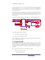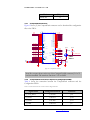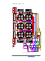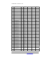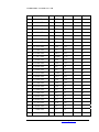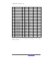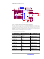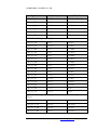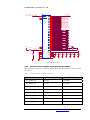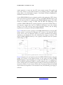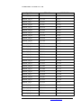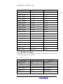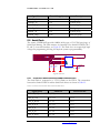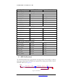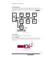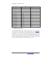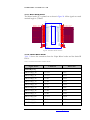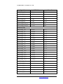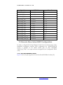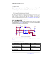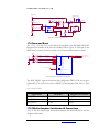
1
THE DINI GROUP LOGIC Emulation Source User Manual DN7006K10PCIe-8T LOGIC EMULATION SOURCE DN7006K10PCIe-8T User Manual Version 1.0 Date of Print February 2, 2009 © The Dini Group 7469 Draper Ave. La Jolla, CA92037 Phone 858.454.3419 • Fax 858.454.1728 [email protected] www.dinigroup.com Copyright Notice and Proprietary Information Copyright © 2008 The Dini Group. All rights reserved. No part of this copyrighted work may be reproduced, modified or distributed in any form or by any means, without the prior written permission of The Dini Group. Right to Copy Documentation The Dini Group permits licensee to make copies of the documentation for its internal use only. Each copy shall include all copyrights, trademarks, disclaimers and proprietary rights notices. Disclaimer The Dini Group has made reasonable efforts to ensure that the information in this document is accurate and complete. However, The Dini Group assumes no liability for errors, or for any incidental, consequential, indirect, or special damages, including, without limitation, loss of use, loss or alteration of data, delays, or lost profits or savings, arising from the use of this document or the product which it accompanies. Table of Contents INTRODUCTION ..................................................................................................................................................................................................................... 1 1 2 3 4 5 DN7006K10PCIE-8T LOGIC EMULATION KIT ............................................................................................................................................. 1 DN7006K10PCIE-8T LOGIC EMULATION BOARD FEATURES ....................................................................................................................... 2 PACKAGE CONTENTS: ..................................................................................................................................................................................... 4 INSPECT THE BOARD ....................................................................................................................................................................................... 5 ADDITIONAL INFORMATION ............................................................................................................................................................................ 5 GETTING STARTED .............................................................................................................................................................................................................. 6 1 2 3 4 1.1 1.2 2.1 2.2 3.1 3.2 BEFORE YOU BEGIN ........................................................................................................................................................................................ 6 Configuring the Programmable Components ......................................................................................................................................................... 6 Warnings ................................................................................................................................................................................................................. 6 INSTALLING THE SOFTWARE ........................................................................................................................................................................... 7 Exploring the Customer CD .................................................................................................................................................................................... 7 Installing the USB GUI Driver ............................................................................................................................................................................... 8 BOARD SETUP ................................................................................................................................................................................................ 12 Before Powering Up the Board............................................................................................................................................................................. 12 Powering Up the Board ........................................................................................................................................................................................ 12 RUNNING THE ONE SHOT TEST.................................................................................................................................................................... 13 INTRODUCTION TO THE SOFTWARE TOOLS............................................................................................................................................................ 16 1 USB CONTROLLER (GUI) ............................................................................................................................................................................. 16 1.1 System Requirements ............................................................................................................................................................................................. 17 1.2 Getting Started with USBController ..................................................................................................................................................................... 17 1.2.1 Main Window................................................................................................................................................................................................ 17 1.2.2 Basic Menu Operations ................................................................................................................................................................................. 18 2 AETEST USB APPLICATION .......................................................................................................................................................................... 18 2.1 Compiling AETest_usb .......................................................................................................................................................................................... 18 3 PCIE AETEST APPLICATION ........................................................................................................................................................................ 19 3.1 Functionality ......................................................................................................................................................................................................... 19 3.2 Running AETEST................................................................................................................................................................................................... 20 3.3 Compiling AETEST (PCIe) ................................................................................................................................................................................... 22 3.3.1 Compiling AETest for Windows XP ............................................................................................................................................................ 22 PROGRAMMING/CONFIGURING THE HARDWARE ................................................................................................................................................. 23 1 2 INTRODUCTION .............................................................................................................................................................................................. 23 PREPARING THE CONFIGURATION FILES ....................................................................................................................................................... 24 2.1 Creating Configuration File “main.txt” ............................................................................................................................................................... 24 2.1.1 Format of “main.txt” ..................................................................................................................................................................................... 24 3 CONFIGURING AN FPGA USING “MAIN.TXT” ................................................................................................................................................ 27 3.1 Setup ...................................................................................................................................................................................................................... 27 3.2 Configuration MSEL Resistors ............................................................................................................................................................................. 27 3.3 HyperTerminal Setup ............................................................................................................................................................................................ 28 3.4 Configuring the FPGA .......................................................................................................................................................................................... 28 3.4.1 Description of Main Menu Options .............................................................................................................................................................. 30 4 CONFIGURING AN FPGA H/W USING USBCONTROLLER ............................................................................................................................. 31 4.1 Setup ...................................................................................................................................................................................................................... 31 4.2 Configuring the FPGA .......................................................................................................................................................................................... 31 5 CONFIGURING AN FPGA USING JTAG.......................................................................................................................................................... 33 5.1 Setup ...................................................................................................................................................................................................................... 33 5.2 Configuring the FPGA .......................................................................................................................................................................................... 33 6 SETTING UP THE CLOCK FREQUENCIES ........................................................................................................................................................ 35 Setup ...................................................................................................................................................................................................................... 35 Configuring the Clock Multipliers using USBController ..................................................................................................................................... 36 Selecting a Clock Source using USBController ................................................................................................................................................... 37 7 UPDATING THE FIRMWARE............................................................................................................................................................................ 38 7.1 Introduction ........................................................................................................................................................................................................... 38 7.2 MCU Startup Modes ............................................................................................................................................................................................. 39 7.3 Updating the USBController ................................................................................................................................................................................ 39 7.4 Updating the Configuration FPGA PROM Firmware ......................................................................................................................................... 39 7.4.1 Using USBController .................................................................................................................................................................................... 39 7.4.2 Using JTAG cable (Xilinx) ........................................................................................................................................................................... 40 7.4.3 Using AEtest_USB........................................................................................................................................................................................ 42 7.5 Updating MCU EEPROM ..................................................................................................................................................................................... 44 7.5.1 Using USBController .................................................................................................................................................................................... 44 7.5.2 Using AETest_USB ...................................................................................................................................................................................... 44 7.6 Updating the MCU (Flash) ................................................................................................................................................................................... 45 7.6.1 Using USBController .................................................................................................................................................................................... 45 7.6.2 Using AETest_USB ...................................................................................................................................................................................... 46 7.7 PCIe “FPGA Q” and SPI Serial Flash ................................................................................................................................................................ 47 7.7.1 Configuring the PCIe FPGA using USBController ...................................................................................................................................... 47 7.7.2 Configuring the PCIe FPGA PROM using USBController ......................................................................................................................... 49 7.7.3 Configuring the PCIe FPGA using JTAG cable (Xilinx) ............................................................................................................................. 50 7.7.4 Configuring the PCIe FPGA PROM using JTAG Cable (Xilinx) ............................................................................................................... 52 7.7.5 Configuring the PCIe FPGA PROM using “main.txt” ................................................................................................................................. 54 6.1 6.2 6.3 HARDWARE DESCRIPTION .............................................................................................................................................................................................. 55 1 2 OVERVIEW ..................................................................................................................................................................................................... 55 ALTERA STRATIX-III FPGAS ........................................................................................................................................................................ 57 2.1 Summary of Stratix-III device features: ................................................................................................................................................................ 58 3 STRATIX-III FPGA CONFIGURATION ............................................................................................................................................................ 59 3.1 Micro Controller Unit (MCU) .............................................................................................................................................................................. 60 3.1.1 MCU EEPROM Interface ............................................................................................................................................................................. 60 3.1.2 MCU SRAM External ................................................................................................................................................................................... 61 3.1.3 MCU Flash .................................................................................................................................................................................................... 61 3.1.4 MCU USB 2.0 Interface................................................................................................................................................................................ 62 3.1.5 RS232 Interface ............................................................................................................................................................................................. 62 3.2 Configuration FPGA ............................................................................................................................................................................................. 63 3.2.1 Configuration PROM/FPGA Programming ................................................................................................................................................. 66 3.2.2 Design Notes on the Configuration FPGA ................................................................................................................................................... 66 3.3 CompactFlash ....................................................................................................................................................................................................... 66 3.3.1 CompactFlash Connector .............................................................................................................................................................................. 67 3.3.2 CompactFlash connection to Spartan-3 (Configuration FPGA) .................................................................................................................. 67 3.4 Stratix-III Boundary-Scan (JTAG) Interface ........................................................................................................................................................ 68 3.4.1 Stratix-III FPGA JTAG Connector ............................................................................................................................................................... 69 3.4.2 Stratix-III FPGA JTAG connection to Configuration FPGA ....................................................................................................................... 69 3.5 Configuration MSEL Resistors ............................................................................................................................................................................. 69 4 CLOCK GENERATION ..................................................................................................................................................................................... 70 4.1 Clock Methodology ............................................................................................................................................................................................... 70 4.2 Stratix-III FPGA Clocking Resources .................................................................................................................................................................. 72 4.3 Clock Multipliers (x4) ........................................................................................................................................................................................... 73 4.3.1 General Clock Multiplier (U41) - CLK_G0 ................................................................................................................................................. 74 4.3.2 Connections between the FPGAs and Clock Multipliers ............................................................................................................................. 78 4.4 Daughter Card (DC) Header Clocks .................................................................................................................................................................... 81 4.4.1 EXT SMA & DCD Global Clocks (U30) ..................................................................................................................................................... 81 4.4.2 DCE & DCF Global Clocks (U45) ............................................................................................................................................................... 81 4.4.3 Connection between FPGAs and External/Daughter Card D, E&F Global Clocks .................................................................................... 82 4.4.4 Secondary Daughter Card (DC) Header Clocks ........................................................................................................................................... 83 4.4.5 Connection between FPGAs and the Secondary DC Header Clocks ........................................................................................................... 84 4.5 PCIe Reference Clocks.......................................................................................................................................................................................... 85 4.5.1 PCIe Reference Clock Circuit ....................................................................................................................................................................... 85 4.5.2 Connection between FPGAs and the PCIe Reference Clock Buffer............................................................................................................ 85 4.6 Main Bus Clock – CLK_MB.................................................................................................................................................................................. 86 4.6.1 Main Bus Clock Circuit ................................................................................................................................................................................ 86 4.6.2 Connection between FPGAs and the Main Bus Clock Buffer ..................................................................................................................... 87 4.7 External SMA Clock Inputs, one per FPGA ......................................................................................................................................................... 88 4.7.1 External SMA Clock Input Circuit (FPGA A) ............................................................................................................................................. 88 4.7.2 Connection between Stratix-III FPGAs and External SMA Connectors ..................................................................................................... 88 4.8 External Clock Test Points, one per FPGA .......................................................................................................................................................... 89 4.8.1 External Clock Test Point Circuit (FPGA A) ............................................................................................................................................... 89 4.8.2 Connection between Stratix-III FPGAs and External Test Points ............................................................................................................... 89 5 MEMORY........................................................................................................................................................................................................ 90 5.1 DDR2 SDRAM SODIMM ...................................................................................................................................................................................... 90 5.1.1 DDR2 Termination........................................................................................................................................................................................ 90 5.1.2 VDD Switching Power Supply (P_SODIMM_x) ........................................................................................................................................... 93 5.1.3 VTT Linear Power Supply (P0.9V_VTT_x) ................................................................................................................................................ 93 5.1.4 Serial Presence-Detect EEPROM Operation ................................................................................................................................................ 93 5.1.5 Clocking Connections between Stratix-III FPGAs and DDR2 SDRAM SODIMMs ................................................................................. 94 5.1.6 SODIMM connections to the Stratix-III FPGAs .......................................................................................................................................... 95 5.1.7 DDR2 PCB Trace Lengths.......................................................................................................................................................................... 112 5.2 Serial Flash ......................................................................................................................................................................................................... 113 5.2.1 Connections between Stratix-III FPGAs and Serial Flash ......................................................................................................................... 113 6 LED INDICATORS ........................................................................................................................................................................................ 114 6.1 User LED’s .......................................................................................................................................................................................................... 115 6.2 Configuration DONE LED.................................................................................................................................................................................. 117 6.3 Ethernet LED’s .................................................................................................................................................................................................... 117 6.4 Power Supply Status LED’s ................................................................................................................................................................................ 118 6.5 Miscellaneous LED’s .......................................................................................................................................................................................... 119 7 RS232 PORT ................................................................................................................................................................................................ 120 7.1.1 RS232 Circuit Diagram ............................................................................................................................................................................... 120 7.1.2 Connections between FPGAs and RS232 Port ........................................................................................................................................... 121 8 TEMPERATURE SENSORS ............................................................................................................................................................................. 121 8.1.1 Temperature Sensor Circuit ........................................................................................................................................................................ 121 8.1.2 Connection between Stratix-III FPGAs and Temperature Sensors ............................................................................................................ 122 9 ETHERNET PHYS ......................................................................................................................................................................................... 123 9.1 Ethernet Interface ................................................................................................................................................................................................ 123 9.1.1 Serial Management Interface ...................................................................................................................................................................... 123 9.1.2 Ethernet LED’s............................................................................................................................................................................................ 124 9.1.3 Timing ......................................................................................................................................................................................................... 124 9.1.4 Ethernet Circuit ........................................................................................................................................................................................... 124 9.1.5 Connections between Stratix-III FPGAs and Ethernet PHYs .................................................................................................................... 124 10 PCIE INTERFACE.......................................................................................................................................................................................... 126 10.1.1 Block Diagram ............................................................................................................................................................................................ 127 10.1.2 Clocking ...................................................................................................................................................................................................... 127 10.1.3 Configuration .............................................................................................................................................................................................. 127 10.1.4 PCIe Power Connector ................................................................................................................................................................................ 128 10.1.5 Connection between Virtex-5 FPGA and Stratix-III FPGA A ................................................................................................................... 128 11 MISCELLANEOUS FPGA IO HEADERS ........................................................................................................................................................ 135 11.1.1 FPGA IO Header Circuit............................................................................................................................................................................. 135 11.1.2 Connections between Stratix-III FPGAs and 10-pin IO Headers .............................................................................................................. 135 12 MICTOR HEADERS ....................................................................................................................................................................................... 137 12.1.1 Mictor Header Circuit ................................................................................................................................................................................. 138 12.1.2 FPGA to Mictor Header .............................................................................................................................................................................. 138 13 REMOTE SLAVE SELECTMAP CONFIGURATION ......................................................................................................................................... 140 13.1.1 Slave SelectMAP Mictor Header ................................................................................................................................................................ 140 13.1.2 Slave SelectMAP Mictor connections to the FPGA ................................................................................................................................... 141 14 FPGA INTERCONNECT ................................................................................................................................................................................ 142 14.1 MainBus (MB) ................................................................................................................................................................................................. 142 14.1.1 MainBus (MB) Header................................................................................................................................................................................ 143 14.2 FPGA-FPGA ................................................................................................................................................................................................... 145 15 POWER MONITORS AND RESET ................................................................................................................................................................... 145 15.1.1 Power Monitor Circuit ................................................................................................................................................................................ 145 15.1.2 Connection between Reset Buffers and FPGAs ......................................................................................................................................... 145 16 POWER DISTRIBUTION ................................................................................................................................................................................. 146 16.1 In-System Operation........................................................................................................................................................................................ 146 16.2 Stand Alone Operation .................................................................................................................................................................................... 147 16.2.1 External Power Connector .......................................................................................................................................................................... 149 17 DAUGHTER CARD HEADERS ....................................................................................................................................................................... 150 17.1 Daughter Card clocking.................................................................................................................................................................................. 150 17.2 Daughter Card Header Pin Assignments ....................................................................................................................................................... 150 17.3 Special Pins on the Daughter Card Header ................................................................................................................................................... 152 17.3.1 GCAp/n, and GCBp/n ................................................................................................................................................................................. 152 17.3.2 VCCIO Power Supply .................................................................................................................................................................................... 152 17.3.3 VCCPD Power Supply .................................................................................................................................................................................... 152 17.4 Power and Reset .............................................................................................................................................................................................. 153 17.5 FPGA to Daughter Card Header IO Connections ......................................................................................................................................... 153 17.6 Insertion/Removal of Daughter Card ............................................................................................................................................................. 174 17.7 MEG-Array Specifications .............................................................................................................................................................................. 176 18 MECHANICAL .............................................................................................................................................................................................. 177 18.1 Board Dimensions ........................................................................................................................................................................................... 177 18.2 Standard Daughter Card Size ......................................................................................................................................................................... 178 18.3 Daughter Card Spacing .................................................................................................................................................................................. 178 APPENDIX 180 19 APPENDIX A: USF FILE .............................................................................................................................................................................. 180 20 ORDERING INFORMATION ........................................................................................................................................................................... 180 21 OPTIONAL EQUIPMENT ................................................................................................................................................................................ 180 21.1 Compatible Dini Group Products ................................................................................................................................................................... 180 21.1.1 Memories ..................................................................................................................................................................................................... 180 21.1.2 Extenders ..................................................................................................................................................................................................... 181 21.1.3 Daughter Cards............................................................................................................................................................................................ 181 21.2 Compatible third-party products .................................................................................................................................................................... 183 22 COMPLIANCE DATA ..................................................................................................................................................................................... 184 22.1 Compliance...................................................................................................................................................................................................... 184 22.1.1 EMI .............................................................................................................................................................................................................. 184 22.1.2 PCIe-SIG ..................................................................................................................................................................................................... 184 22.2 Environmental ................................................................................................................................................................................................. 184 22.2.1 Temperature ................................................................................................................................................................................................ 184 22.3 Export Control................................................................................................................................................................................................. 184 22.3.1 Lead-Free .................................................................................................................................................................................................... 184 22.3.2 The USA Schedule B number based on the HTS ....................................................................................................................................... 184 22.3.3 Export control classification number ECCN .............................................................................................................................................. 184 List of Figures Figure 1 - DN7006K10PCIe-8T Logic Emulation Board ................................................................................................................................................................................... 2 Figure 2 - DN7006K10PCIe-8T CD ROM Directory Structure ....................................................................................................................................................................... 7 Figure 3 - CompactFlash Directory Listing ......................................................................................................................................................................................................... 27 Figure 4 - MSEL Configuration Resistors (default FPP) ................................................................................................................................................................................... 27 Figure 5 - DN7006K10PCIe-8T Logic Emulation Board Block Diagram..................................................................................................................................................... 56 Figure 6 - MCU EEPROM Interface.................................................................................................................................................................................................................... 61 Figure 7 - MCU SRAM............................................................................................................................................................................................................................................ 61 Figure 8 - MCU Flash .............................................................................................................................................................................................................................................. 62 Figure 9 - USB Connector ...................................................................................................................................................................................................................................... 62 Figure 10 – MCU/Configuration FPGA Serial Port .......................................................................................................................................................................................... 63 Figure 11 – Configuration PROM/FPGA Programming Header ................................................................................................................................................................... 66 Figure 12 - CompactFlash Connector................................................................................................................................................................................................................... 67 Figure 13 - FPGA JTAG Connector .................................................................................................................................................................................................................... 69 Figure 14 - MSEL Configuration Resistors (default FPP)................................................................................................................................................................................. 70 Figure 15 - Clocking Block Diagram ..................................................................................................................................................................................................................... 71 Figure 16 - Stratix-III FPGA Dedicated Clock Inputs ...................................................................................................................................................................................... 73 Figure 17 - Clock Multiplier Circuit ...................................................................................................................................................................................................................... 78 Figure 18 – External, -Daughter Card D Global Clock Input Circuit ............................................................................................................................................................ 81 Figure 19 – Daughter Card D & E Global Clock Input Circuit....................................................................................................................................................................... 82 Figure 20 – Secondary Daughter Card (DC) Header Clock.............................................................................................................................................................................. 84 Figure 21 – PCIe Reference Clock Circuit ........................................................................................................................................................................................................... 85 Figure 22 – Main Bus Clock Buffer....................................................................................................................................................................................................................... 87 Figure 23 – Stratix-III FPGA SMA Clock Input Circuit ................................................................................................................................................................................... 88 Figure 24 - External Clock Test Point Circuit ..................................................................................................................................................................................................... 89 Figure 25 - Write Operation Using Parallel ODT and 50- Series OCT of the Stratix-III FPGA Device .............................................................................................. 91 Figure 26 - Read Operation from DDR2 SDRAM Memory Using the Parallel OCT Feature of the Stratix-III .................................................................................... 92 Figure 27 - VDD Switching Power Supply (P_SODIMM_A) ......................................................................................................................................................................... 93 Figure 28 - VTT Linear Power Supply (P0.9V_VTT_A) .................................................................................................................................................................................. 93 Figure 29 - Serial Flash .......................................................................................................................................................................................................................................... 113 Figure 30 - LED Indicator .................................................................................................................................................................................................................................... 114 Figure 31 – MCU/Configuration FPGA Serial Port ........................................................................................................................................................................................ 120 Figure 32 - Temperature Sensor (FPGA A)....................................................................................................................................................................................................... 122 Figure 33 - Ethernet Circuit (FPGA D) ............................................................................................................................................................................................................. 124 Figure 34 - PCIe Bus Diagram ............................................................................................................................................................................................................................. 127 Figure 35 - Virtex-5 SPI Serial Flash ................................................................................................................................................................................................................... 127 Figure 36 - PCIe Power Connection ................................................................................................................................................................................................................... 128 Figure 37 - Stratix-III FPGA IO Header (FPGA D) ....................................................................................................................................................................................... 135 Figure 38 - 38 Pin Mictor Header on FPGA C ................................................................................................................................................................................................. 138 Figure 39 – Slave SelectMAP Mictor Header .................................................................................................................................................................................................... 141 Figure 40 - MainBus Interconnect ....................................................................................................................................................................................................................... 143 Figure 41 - MainBus Header................................................................................................................................................................................................................................. 144 Figure 42 - Low Voltage Comparator Circuit .................................................................................................................................................................................................... 145 Figure 43 – PCIe Edge Connector ...................................................................................................................................................................................................................... 147 Figure 44 - ATX Power Supply............................................................................................................................................................................................................................ 149 Figure 45 - External Power Connection ............................................................................................................................................................................................................. 149 Figure 46 - Daughter Card Header Bank/Pin Assignments ........................................................................................................................................................................... 151 Figure 47 - VCCIO Adjustable Linear Power Supply (x4) .................................................................................................................................................................................. 152 Figure 48 - VCCPD Voltage Select Circuit ........................................................................................................................................................................................................ 153 Figure 49 - Daughter Card Header Power & RESET...................................................................................................................................................................................... 153 List of Tables Table 1 - CD ROM Directory Contents ................................................................................................................................................................................................................. 7 Table 2 – Main.txt Command List......................................................................................................................................................................................................................... 25 Table 3 – Stratix-III Configuration Schemes ....................................................................................................................................................................................................... 28 Table 4: HyperTerminal Main Menu Options .................................................................................................................................................................................................... 30 Table 5 - FPGA configuration file size ................................................................................................................................................................................................................. 66 Table 6 - Connection between the CF connector and the Configuration FPGA ......................................................................................................................................... 67 Table 7 – Stratix-III FPGA JTAG connection to Configuration FPGA........................................................................................................................................................ 69 Table 8 – Stratix-III Configuration Schemes ....................................................................................................................................................................................................... 70 Table 9 - Clock Multiplier Frequency Parameters............................................................................................................................................................................................... 74 Table 10 - Connections between FPGAs and Clock Multipliers ..................................................................................................................................................................... 78 Table 11 - Connections between FPGAs and External/Daughter Card E & F Clocks .............................................................................................................................. 82 Table 12 - Connections between FPGAs and Secondary DC Header Clocks ............................................................................................................................................... 84 Table 13 - Connection between FPGA and PCIe Reference Clock Buffer ................................................................................................................................................... 85 Table 14 - Connection between FPGA and Main Bus Clock Buffers............................................................................................................................................................. 87 Table 15 - Connection between Stratix-III FPGAs and External SMA Connectors.................................................................................................................................... 88 Table 16 - Connection between Stratix-III FPGAs and External Test Points .............................................................................................................................................. 89 Table 17 - DDR2 Termination ............................................................................................................................................................................................................................... 92 Table 18 - Serial Presence-Detect EEPROM Connections .............................................................................................................................................................................. 94 Table 19 – Clocking Connections between Stratix-III FPGAs and the DDR2 SDRAM SODIMMs ...................................................................................................... 95 Table 20 - Connections between the Stratix-III FPGAs and the SODIMMs ............................................................................................................................................... 95 Table 21 – DDR2 PCB Trace Lengths ............................................................................................................................................................................................................... 112 Table 22 - Connections between Stratix-III FPGA and the Serial Flash Devices ...................................................................................................................................... 113 Table 23 – User LED’s .......................................................................................................................................................................................................................................... 115 Table 24 – FPGA DONE LED .......................................................................................................................................................................................................................... 117 Table 25 – Power Supply Status LED’s .............................................................................................................................................................................................................. 118 Table 26 – Power Supply Status LED’s .............................................................................................................................................................................................................. 118 Table 27 – Miscellaneous LED’s ......................................................................................................................................................................................................................... 119 Table 28 - Connections between FPGAS and the RS232 Port ...................................................................................................................................................................... 121 Table 29 - Connection between Stratix-III FPGAs and Temperature Sensors ........................................................................................................................................... 123 Table 30 - Connection between Stratix-III FPGAs and Ethernet PHYs ..................................................................................................................................................... 125 Table 31 – PCIe Bandwidth.................................................................................................................................................................................................................................. 126 Table 32 - Connection between Virtex-5 FPGA and Stratix-III FPGA A ................................................................................................................................................... 128 Table 33 - Connection between Stratix-III FPGAs and 10-pin IO Headers ............................................................................................................................................... 135 Table 34 - Connections between FPGAs and Mictor Headers ...................................................................................................................................................................... 138 Table 35 – Slave SelectMAP Mictor connections to the FPGA..................................................................................................................................................................... 141 Table 36 - Connection between Reset Buffers and FPGAs ............................................................................................................................................................................ 145 Table 37 – Daughter Card Reset .......................................................................................................................................................................................................................... 153 Table 38 - FPGA to Daughter Card Header IO Connections ....................................................................................................................................................................... 154 1 Chapter I N T R O D U C T I O N Introduction This User Manual accompanies the DN7006K10PCIe-8T Stratix-III Logic Emulation Board. For specific information regarding the Stratix-III parts, please reference the datasheet on the Altera website. 1 DN7006K10PCIe-8T LOGIC Emulation Kit The DN7006K10PCIe-8T Stratix-III Logic Emulation Board provides a hardware platform for developing and prototyping low-power, high-performance, logic-intensive designs. The board provides a wide range of peripherals and memory interfaces to facilitate the design and development of Stratix-III designs. The DN7006K10PCIe-8T can hosted in an 8-lane PCIe (GEN1) system or operate in standalone mode using the USB/CompactFLASH interface. A single DN7006K10PCIe-8T configured with 6 Altera Stratix-III FPGAs (EP3SL340) can emulate up to 15 million gates of logic as measured by a reasonable ASIC gate counting standard and this number does not include embedded memories and multipliers resident in each FPGA. One hundred percent (100%) of the EP3SL340's FPGA resources are available to the user application. The DN7006K10PCIe-8T achieves high gate density and allows for fast target clock frequencies by utilizing the largest FPGA from Altera's Stratix-III family. The DN7006K10PCIe-8T is supplied with a full function, fixed, 8-lane PCIe master/target. Drivers and 'C' source for several operating systems are included. DN7006K10PCIE8T User Manual www.dinigroup.com 1 I N T R O D U C T I O N 2 DN7006K10PCIe-8T Logic Emulation Board Features Figure 1 - DN7006K10PCIe-8T Logic Emulation Board DN7006K10PCIe-8T Stratix-III Board features the following: • Altera Stratix-III FPGAs (FF1760), -2, -3, -4 Speed Grade o EP3SL340 (x6) • FPGA to FPGA interconnect, Single-ended and LVDS o 600MHz Chip-to-Chip o Source Synchronous Clocking for LVDS • Flexible Clock Resources o FPGA Clock Multipliers - Si5326 (x3) General Clock Network DN7006K10PCIe-8T User Manual www.dinigroup.com 2 I N T R O D U C T I O N LVDS Clock Network DDR2 Clock Network o GTP Transceiver Clock Multiplier - Si5326 (x1) o External FPGA Clock (LVDS) Input via SMA’s (x1) o Multiple clocks from the Daughter Card Headers (P4, P5, P6) o Global clocks from Spartan and Virtex-5 FPGAs o Clock Test Points (x6) • FPGA Configuration (Stratix-III) o JTAG/Boundary-Scan configuration mode o Fast Passive Parallel (FPP) using the Spartan Configuration FPGA o CompactFLASH, USB and PCIe configuration options • Memory o DDR2, 512MB (64Meg x 64), 200pin SODIMM (PC2-4200), support up to 4GB (x4) o Serial FLASH Memory, 16Mbit (4096 pages of 512/528 bytes/page) • High Speed Transceiver (Virtex-5) o PCIe GEN 1 (x8) • User LED’s • Onboard Distributed Power Supplies • Daughter Card Headers (x3) LVDS – MEG-Array (400 pin) • Full support for Embedded Logic Analyzers o SignalTapTM Logic Analyzer • Shared RS232 Port, 10 pin Header DN7006K10PCIe-8T User Manual www.dinigroup.com 3 I N T R O D U C T I O N • Stand Alone operation, requires an external +12V ATX power supply with a PCIe power connector. 3 Package Contents: Before using the kit or installing the software, be sure to check the contents of the kit and inspect the board to verify that you received all of the items. If any of these items are missing, contact The Dini Group before you proceed. The DN7006K10PCIe-8T Logic Emulation Board kit includes the following: • 256MB CompactFLASH Card • USB FLASH Memory Card Reader • USB 2.0 Cable • RS232 DB9(F) to IDC Header Cable • RS232 Serial Cable (DB9), 6ft, F/F • 6-Pin PSU Adaptor for PCIe Video Cards • Daughter Card Mounting Hardware o Screw, Machine M3x5mm (x8) o Nut, HEX M3 (x8) o Spacer, M3x14mm • CD ROM containing: o USB Application Program (usbcontroller.exe) o PCIe Program (aetest.exe) o Stratix-III Reference Designs (Verilog) o User Manual (pdf format) o Schematic (pdf format) o Component Datasheets (pdf format) Optional items that support development efforts (not provided): DN7006K10PCIe-8T User Manual www.dinigroup.com 4 I N T R O D U C T I O N 9 Altera Quartus-II Software 9 Altera USB-Blaster Download Cable 9 DDR2 SODIMMs (Available upon request) 4 Inspect the Board Place the board on an anti-static surface and inspect it to ensure that it has not been damaged during shipment. Verify that all components are on the board and appear intact. 5 Additional Information For additional information, please visit http://www.dinigroup.com/. The following table lists some of the resources you can access from this website. You can also directly access these resources using the provided URLs. Resource Description/URL User Manual This is the main source of technical information. The manual should contain most of the answers to your questions Demonstration Videos MEG-Array Daughter Card header insertion and removal video Dini Group Web Site The web page will contain the latest user manual, application notes, FAQ, articles, and any device errata and manual addenda. Please visit and bookmark: http://www.dinigroup.com Data Book Pages from Stratix-III Databook, which contains device-specific information on Altera device characteristics E-Mail You may direct questions and feedback to the Dini Group using this e-mail address: [email protected] Phone Support Call us at 858.454.3419 during the hours of 8:00am to 5:00pm Pacific Time. FAQ The download section of the web page may contain a document called DN7006K10PCIe-8T Frequently Asked Questions (FAQ). This document is periodically updated with information that may not be in the User’s Manual. DN7006K10PCIe-8T User Manual www.dinigroup.com 5 G E T T I N G 2 Chapter S T A R T E D Getting Started Congratulations on your purchase of the DN7006K10PCIe8T Stratix-III Logic Emulation Board. The remainder of this chapter describes how to start using the DN7006K10PCIe-8T Logic Emulation Board. 1 Before You Begin 1.1 Configuring the Programmable Components The DN7006K10PCIe-8T has been factory tested and pre-programmed to ensure correct operation. The user does not need to alter any jumpers or program anything to see the board work. 1.2 Warnings • Daughter Card Test Headers (Over Voltage) - The 400-pin daughter card test headers are NOT 5V tolerant. Take care when handling the board to avoid touching the components and daughter card connections due to ESD. • ESD Warning - The board is sensitive to static electricity, so treat the PCB accordingly. The target markets for this product are engineers that are familiar with FPGAs and circuit boards. However, if needed, the following web page has an excellent tutorial on the “Fundamentals of ESD” for those of you who are new to ESD sensitive products: http://www.esda.org/basics/part1.cfm • Operating Temperature - Avoid touching the PTH012050WAZ power supply modules (PSU1, PSU2, PSU3, PSU12, PSU13, and PSU 14) as they operate at high temperatures and may cause skin burns. DN7006K10PCIe-8T User Manual www.dinigroup.com 6 G E T T I N G S T A R T E D 2 Installing the Software For complete information regarding the USB Graphical User Interface (GUI) and installation instructions, see the “USB Controller Manual” available from The Dini Group website. 2.1 Exploring the Customer CD The DN7006K10PCIe-8T CD ROM contains the following items (the CD ROM does not auto-install on the customer machine), see Figure 2: <installation directory> Config_Section_Code Datasheets DNMEG_Intercon_Daughtercard DNMEG_Observation_Daughtercard Documentation FPGA_Reference_Designs PCIe_Software_Applications Schematics USB_Software_Applications Figure 2 - DN7006K10PCIe-8T CD ROM Directory Structure A description of the CD ROM directory contents is listed in Table 1. Please visit The Dini Group website for the most recent revision of these documents. Table 1 - CD ROM Directory Contents CD ROM Directory Contents Directory Name Description of Contents Config_Section_Code Configuration source code, not intended to be used by the customer. Datasheets Datasheets for all the components used on the board. DN7006K10PCIe-8T User Manual www.dinigroup.com 7 G E T T I N G S T A R T E D DNMEG_Intercon_Daughtercard The DNMEG_Intercon is a daughter card that bridges the expansion signals between two 400-pin MEG-Array connectors. DNMEG_Observation_Daughtercard The DNMEG_Obs Observation Daughter card is a complete solution for observation of signals on the 400-pin MEG-Array connector. Documentation Contains this document and other project related documentation. FPGA_Reference_Designs Contains the source and compiled programming files for the DN7006K10PCIe8T reference designs. PCIe_Software_Applications Source and binary files for the PCIe-HOST application. Schematics PDF version of the board schematic. A netlist that contains all nets on the board that connects to user IO on any FPGA. USB_Software_Applications Source and binary files for USB Controller applications. 2.2 Installing the USB GUI Driver When the DN7006K10PCIe-8T power on, and you connect it to a USB port for the first time, the pop-up window will ask you to install a driver. The driver installation instructions for Windows XP system are shown below: • Select “No, not this time” to search for software. DN7006K10PCIe-8T User Manual www.dinigroup.com 8 G E T T I N G S T A R T E D • Select “Install from a list or specific location (Advanced)” and click “Next” to continue. • Select “Don’t search. I will choose the driver to install” and click “Next” to continue. DN7006K10PCIe-8T User Manual www.dinigroup.com 9 G E T T I N G S T A R T E D • Select “Have Disk…” and direct the browse window to location “..\USB_Software_Applications\driver\windows_wdm” on the CD ROM. • A new window will display the list of compatible hardware, click “Next” to continue. DN7006K10PCIe-8T User Manual www.dinigroup.com 10 G E T T I N G S T A R T E D • The Windows software will then install the driven assigned to the hardware. • After successful installation of the driver the following window will be displayed. DN7006K10PCIe-8T User Manual www.dinigroup.com 11 G E T T I N G S T A R T E D 3 Board Setup The instructions in this section explain how to install the DN7006K10PCIe-8T Logic Emulation Board. For the purpose of this demonstration, the DN7006K10PCIe-8T will be configured in Stand-Alone mode. 3.1 Before Powering Up the Board Before powering up the board, prepare the board as follows: 1. Attach an ATX Power Supply to the PCIe Power Header (J7) on the DN7006K10PCIe-8T Logic Emulation Board using the PCIe “Graphics Power” adaptor cable. 2. Connect the USB Cable from the host computer to the USB Connector (J3). Ensure the USB Controller driver has been installed. 3. If the kit contains Memory SODIMMs, populate the SODIMM sockets (J8, J9, J39, and J40) with the required modules. Do not insert the SODIMM module with the board powered. 3.2 Powering Up the Board Power up the board by turning ON the ATX power supply and verify the Power ON LED (DS25) is ON indicating the presence of +12V (located at the bottom left of the PCB by the PCIe edge connector). DN7006K10PCIe-8T User Manual www.dinigroup.com 12 G E T T I N G S T A R T E D 4 Running the One SHOT Test The Dini Group provides a USB Controller application on the CD ROM (..\USB_Software_Applications\USBController\USBController.exe). 1. Open “USBController.exe” and verify that the board was correctly identified as a “DN7006K10PCIE8T” in the log window. 2. Click on “Production Tests” button and select the “One Shot Test” option. Configure the “One Shot Test” as follows (ensure that the path to the bitfiles are correct): DN7006K10PCIe-8T User Manual www.dinigroup.com 13 G E T T I N G S T A R T E D 3. The FPGAs will now be configured and the “One Shot Test” will test the following functions of the board, see transaction Log for more details: • Single Ended Interconnect • LVDS Interconnect • FLASH Test • Clock Readback • Other Miscellaneous One Shot Tests DN7006K10PCIe-8T User Manual www.dinigroup.com 14 G E T T I N G S T A R T E D 4. Successful testing of the DN7006K10PCIe-8T results in the following message being displayed: ***ONE SHOT TEST PASSED!*** OST Ran 1 times, requested to run 1, failed 0 times One Shot Test Finished Execution Time = 800.984 seconds DN7006K10PCIe-8T User Manual www.dinigroup.com 15 I N T R O D U C T I O N T O T H E S O F T W A R E T O O L S 3 Chapter Introduction to the Software Tools This chapter introduces the software tools that are shipped with the DN7006K10PCIe-8T Logic Emulation Board. 1 USB Controller (GUI) The “USBController” is a powerful software application for interfacing between USBEnabled Dini Group products and a host system. It allows the user to program the board’s FPGAs, access global memory registers, read and program clocks, run tests, and more. “USBController” can be used to run various production tests on the boards to ensure that they are working properly. It can also be used for setting up board features, i.e. when running a custom design etc. All “USBController” source code is included on the CD-ROM shipped with the DN7006K10PCIe-8T Logic Emulation Kit. The “USBController” application contains the following functionality: • Configure FPGA(s) over USB • Configure FPGA(s) via CompactFLASH • Clear FPGA(s) • Reconfigure FPGA(s) • Reset FPGA(s) • Read/Write to/from MainBus Address Space • Retrieve Board/MCU/Spartan Version/Serial Number DN7006K10PCIe-8T User Manual www.dinigroup.com 16 I N T R O D U C T I O N T O T H E S O F T W A R E • Read FPGA Temperatures • Setup Clock Frequencies • Update Firmware (MCU and Spartan) • Run Production Tests T O O L S 1.1 System Requirements “USB Controller” can be installed on a Windows 2000/XP system with USB 2.0 capability. 1.2 Getting Started with USBController Once “USBController” is installed, the DN7006K10PCIe-8T is powered ON and the USB cable is plugged in, the user can open “USBController”. The “USBController” application should immediately find the DN7006K10PCIe-8T. If “USBController” does not find the DN7006K10PCIe-8T, the user will get the following alert: 1.2.1 Main Window If the “USBController” finds the DN7006K10PCIe-8T and the USB cable was plugged into the PC before power was turned on to the DN7006K10PCIe-8T the following screen will be displayed: DN7006K10PCIe-8T User Manual www.dinigroup.com 17 I N T R O D U C T I O N 1.2.2 T O T H E S O F T W A R E T O O L S Basic Menu Operations Please refer to the “USB Controller Manual” on the CD ROM for a complete description all the “USBController” functions. 2 AETest USB Application The command line USB controller program is called “AETEST_USB”. It provides a subset of the features available on USB Controller and is cross platform. This program is a convenient place to start if you are going to be writing a custom IO controller for USB to communicate with the DN7006K10PCIe-8T. 2.1 Compiling AETest_usb AETest_usb can be compiled using Microsoft Visual Studio 6 or later, or on any version of Linux that supports the usbdevfs library. DN7006K10PCIe-8T User Manual www.dinigroup.com 18 I N T R O D U C T I O N T O T H E S O F T W A R E T O O L S A make file is provided, but you must un-comment one of the following lines to define which operating system you are running. In Windows, you should run nmake. #DESTOS = WIN_WDM #DESTOS = LINUX #DESTOS = SOLARIS 3 PCIe AETEST Application AETEST utility program can test and verify the functionality of the DN7006K10PCIE-8T Logic Emulation board, and provide data transfer to and from the User design. All AETEST source code is included on the CD-ROM shipped with your DN7006K10PCIE-8T Logic Emulation kit. AETEST can be installed on a variety of operating systems, including: • Windows 2000/XP/Vista (Windows WDM) • Linux 3.1 Functionality All communication to the board using this program is over PCI express. In this way, the basic functionality of PCI Express is tested. The AETEST utility program contains the following tests: • DMA and BAR accesses over PCI Express (When using the full function design for LXT) • DDR2 Memory Test • Flash Test • AETEST also provides the user with the following abilities: • Recognize the DN7006K10PCIE-8T • Display Vendor and Device ID • Set PCIe Device and Function Number • Display all configured PCIe devices DN7006K10PCIe-8T User Manual www.dinigroup.com 19 I N T R O D U C T I O N T O T H E S O F T W A R E T O O L S • Various loops for PCIe device-function and ID numbers • Write and Read Configuration DWORD (for board settings) • Access to the “Main Bus” interface. BAR Memory operations • Configure/Save BARs from/to a file Configure FPGAs. 3.2 Running AETEST The following images show a terminal session in Windows XP. The initial display of AETest shows the results of its scan of the PCIe bus. If the driver for the DN7006K10PCIE-8T is not installed, then the software will display a message that no device was found. If this occurs, (and you are using windows), look into the computer’s hardware manager and see if a PCI Device with Vendor ID 0x17DF appears. If it does then there is a software or driver problem. If it does not then there is a hardware problem. Look on the board near the 6-pin PCI Express power connector. There is a row of LEDs corresponding to the PCI Express status signals. RED LEDs for LOS indicated the board is not linking with its link partner. Yellow is activity. Three green LEDs a valid link in 1x, 4x or 8x mode respectively. DN7006K10PCIe-8T User Manual www.dinigroup.com 20 I N T R O D U C T I O N T O T H E S O F T W A R E T O O L S This is the PCI menu. It can help you debug a software problem detecting or communicating with the board. This is the memory menu. From here you can communicate with the User design in any of the FPGAs (using Main Bus) or directly to FPGA A. DN7006K10PCIe-8T User Manual www.dinigroup.com 21 I N T R O D U C T I O N T O T H E S O F T W A R E T O O L S This is the production tests menu. This is used to debug hardware failures. Here is the board failing the PCIe test. 3.3 3.3.1 Compiling AETEST (PCIe) Compiling AETest for Windows XP AETest for Windows requires visual studio 6 or later to compile. Open the provided make file and uncomment the lines #DESTOS = WIN_WDM Run nmake. DN7006K10PCIe-8T User Manual www.dinigroup.com 22 P R O G R A M M I N G / C O N F I G U R I N G T H E H A R D W A R E 4 Chapter Programming/Configuring the Hardware This chapter details the programming and configuration instructions for the DN7006K10PCIe-8T Logic Emulation Board. 1 Introduction The Dini Group developed the CompactFlash Configuration Environment to address the need for a space-efficient, pre-engineered, high-density configuration solution for systems with single or multiple FPGAs. The technology is a groundbreaking in-system programmable configuration solution that provides substantial savings in development effort and cost per bit over traditional PROM and embedded solutions for highcapacity FPGA systems. Stratix-III devices are configured by loading application-specific configuration data— the bitstream—into internal memory. On the DN7006K10PCIe-8T this can be accomplished via the CompactFlash, PCIe or USB interface using Fast Passive parallel (FPP) configuration option. Because Altera FPGA configuration memory is volatile, it must be configured each time it is powered-up. The bitstream is loaded into the device through special configuration pins. These configuration pins serve as the interface for a number of different configuration modes (the following are supported on this board): • Fast Passive Parallel (FPP) • Fast Passive Parallel (FPP) with design security feature and/or decompression enabled • JTAG/Boundary-Scan configuration mode DN7006K10PCIe-8T User Manual www.dinigroup.com 23 P R O G R A M M I N G / C O N F I G U R I N G • T H E H A R D W A R E Remote Slave SelectMAP (parallel) configuration mode (x8), using the Mictor interface – used to configure daughter cards using selectMAP The JTAG/Boundary-Scan configuration interface is always available, regardless of the Mode pin settings. The JTAG/Boundary-Scan configuration mode disables all other configuration modes to prevent conflicts between configuration interfaces. Certain configuration pins are dedicated to configuration, while others are dual-purpose, see datasheet. Dual-purpose pins serve both as configuration pins and as user I/O after configuration. Dedicated configuration pins retain their function after configuration. The remainder of this section describes the functional blocks that entail the FPGA configuration environment. 2 Preparing the Configuration Files Using the CompactFlash card is the preferred method to configure the FPGAs. To control which bit file on the CompactFlash card is used to configure which FPGA, a file named “main.txt” must be created and copied to the root directory of the CompactFlash card. The configuration process from the CompactFlash card cannot be performed without this file. 2.1 Creating Configuration File “main.txt” The “main.txt” interface is used to control/program the following features on the DN7006K10PCIe-8T Logic Emulation Board: • Basic Features o Configure FPGAs o Setup Clock Frequencies and MUX Settings o RS232 Monitor (Verbose Level) • Advanced Features o MainBus Read/Write Transactions o Configuration Register Read/Write Transactions Below is an example of a “main.txt” file, a description of the options that can be set, and the format this file needs to follow. 2.1.1 Format of “main.txt” The “main.txt” file contains a list of commands, separated by newline characters. A list of valid “main.txt” commands is given below: DN7006K10PCIe-8T User Manual www.dinigroup.com 24 P R O G R A M M I N G / C O N F I G U R I N G T H E H A R D W A R E //<comment> SANITY CHECK: <y/n> VERBOSE LEVEL: <level> FPGA A:<filename> FPGA B:<filename> FPGA C:<filename> FPGA D:<filename> FPGA E:<filename> FPGA F:<filename> CLOCK FREQUENCY: <clock> <number> [MHz] CLOCK FREQUENCY: <clock> <number> [MHz] CLOCK FREQUENCY: <clock> <number> [MHz] MEMORY MAPPED: 0x<WORDADDR> 0x<BYTE> SOURCE: G0 2 DCLK: DC2 100MHZ MAIN BUS: 0x<DWORDADDR> 0x<DWORDDATA> Table 2 describes the function of each of the available “main.txt” commands: Table 2 – Main.txt Command List Instruction // <comment> Function Comments are allowed with the following rules: • All comments must start at the beginning of the line • All comments must begin with // • If a comment spans multiple lines, then each line should start with // Commented lines will be ignored during configuration, and are only for the user’s purpose. SANITY CHECK: <y/n> If <y/n> is set to y, then the MCU will examine the headers in the .bit files on the CompactFlash card before using them to configure each FPGA. If the target FPGA annotated in the .bit file header is not the same type as the FPGA the MCU detects on the board, it will reject the file and flash the error LED. Before this command is executed, <y/n> is set to the default value y. If you want to encrypt of compress your bit files, you will need to set <y/n> to n. VERBOSE LEVEL: <level> During the configuration process, there are three different verbose levels that can be selected for the serial port messages: • DN7006K10PCIe-8T User Manual Level 0: o Fatal error messages o Bit file errors (e.g., bit file was created for the wrong part, bit file was created with wrong version of Xilinx tools, or bitgen options are set incorrectly) o Initializing message will appear before configuration www.dinigroup.com 25 P R O G R A M M I N G / C O N F I G U R I N G T H E Instruction H A R D W A R E Function o • • A single message will appear once the FPGA is configured Level 1: o All messages that Level 0 displays o Displays configuration type (should be SelectMAP) o Displays current FPGA being configured if the configuration type is set to SelectMAP o Displays a message at the completion of configuration for each FPGA configured. Level 2: o All messages that Level 1 displays o Options that are found in “main.txt” o Bit file names for each FPGA as entered in main.txt o Maker ID, device ID, and size of Smart Media card o All files found on Smart Media card o If sanity check is chosen, the bit file attributes will be displayed (part, package, date, and time of the bit file) During configuration, a “.” will be printed out after each block (16 KB) has successfully been transferred from the Smart Media to the current FPGA FPGA A:<filename> For each FPGA the user would like to configure, there must be one line e.g. FPGA “A” will be configured with the file named by <filename> CLOCK FREQUENCY: <clock> <number>MHz The MCU will adjust the clock multiplier producing clock < clock > to the frequency <number>. Valid clock names are G0, G1, and G2 DCLK: DC<dc source> [<n>Mhz] For valid combinations, please see the diagram in par 4.4Daughter Card (DC) Header Clocks of this document. MEMORY MAPPED: 0x<WORDADDR> 0x<BYTE> Writes to a configuration Register. This command can be used to access features that do not have a main.txt command. Example applications include setting clock sources, settings the EXT0 or EXT1 clock buffers to zero‐delay mode, or setting the clocks to frequencies lower than 31Mhz. MAIN BUS 0x<DWORDADDR> 0x<DWORDDATA> Writes data in <DWORDDATA> to the address on the main bus interface at <DWORDADDR>. This command only makes sense in the context of the Dini Group reference design, unless your design implements a compatible controller on the main bus pins. The Specification for this interface is in MainBus section Source: <clock> <n> Sets <clock> to run from source <n>, where n=1 corresponds to normal operation and n=2 corresponds to bypass mode output. Clock can be “G0”,”G1”,”G2”. DN7006K10PCIe-8T User Manual www.dinigroup.com 26 P R O G R A M M I N G / C O N F I G U R I N G T H E H A R D W A R E 3 Configuring an FPGA using “main.txt” This section lists detailed instructions for programming the Altera Stratix-III FPGAs using “main.txt”. Before configuring the FPGAs, ensure that the FPGA bitfiles and “main.txt” has been copied to the root directory of the CompactFlash card, see Figure 3. Figure 3 - CompactFlash Directory Listing 3.1 Setup Before configuring the FPGA, ensure the following steps have been completed: 1. Attach an ATX Power Supply to the PCIe Power Header (J7) on the DN7006K10PCIe-8T Logic Emulation Board using the PCIe “Graphics Power” adaptor cable. 2. Connect the “RS232 Cable” to the “RS232 MCU” header (P2) on the DN7006K10PCIe-8T (this is not required but allows the user to observe the configuration process). 3.2 Configuration MSEL Resistors Fast Passive Parallel (FPP) is the default configuration mode for DN7006K10PCIe-8T. The configuration mode is selected by setting the appropriate level on the dedicated Mode input pins MSEL[2:0] on the FPGAs. P2.5VD R523 (DNI-100R) FPGA_MSEL0 R524 R492 R496 1K 0R 0R FPGA_MSEL1 FPGA_MSEL2 Figure 4 - MSEL Configuration Resistors (default FPP) DN7006K10PCIe-8T User Manual www.dinigroup.com 27 P R O G R A M M I N G / C O N F I G U R I N G T H E H A R D W A R E Select the configuration scheme by driving the Stratix-III device MSEL pins either HIGH or LOW as shown in Table 8. Table 3 – Stratix-III Configuration Schemes Configuration Mode Fast Passive Parallel (FPP) – Factory Default FPP with design Security feature and/or decompression enabled JTAG MSEL[2:0] 000 Configuration Resistors R524, R492, R496 Installed 001 R523, R492, R496 Installed Do not leave MSEL pins floating. R524, R492, R496 Installed 3.3 HyperTerminal Setup Connect the RS232 Serial cable to a COM port on the Host Computer and configure HyperTerminal to the following settings: 3.4 Configuring the FPGA To configure the Stratix-III FPGAs, perform the following steps: 1. Insert the CompactFlash card into the CompactFlash socket (J5). DN7006K10PCIe-8T User Manual www.dinigroup.com 28 P R O G R A M M I N G / C O N F I G U R I N G T H E H A R D W A R E 2. Open a HyperTerminal Window on the Host Computer. 3. Power up the board by turning ON the ATX power supply and verify the Power ON LED (DS25) is ON indicating the presence of +12V (located at the bottom left of the PCB by the PCIe edge connector). 4. Monitor the configuration process in the HyperTerminal window. 5. After successful configuration process the “DN7006K10PCIe-8T Main Menu” will be displayed. The HyperTerminal interface gives the user an easy method for handling and monitoring the DN7006K10PCIe-8T configuration. DN7006K10PCIe-8T User Manual www.dinigroup.com 29 P R O G R A M M I N G / C O N F I G U R I N G 3.4.1 T H E H A R D W A R E Description of Main Menu Options Table 4 describes the Main Menu options found on the MCU HyperTerminal interface. Table 4: HyperTerminal Main Menu Options Option Function Description 1 Configure FPGAs Using “main.txt” The FPGAs will be configured using Fast Passive Parallel (FPP). 2 Interactive configuration menu This option takes you to a menu titled “Interactive Configuration Menu” and allows the FPGAs to be configured through a set of menu options instead of using the main.txt file. 3 Check Configuration Status This option checks the status of the DONE pin and prints out whether or not the FPGAs have been configured along with the file name that was used for configuration. 4 Change MAIN configuration file By default, the processor uses the file main.txt to get the name of the bit file to be used for configuration as well as options for the configuration process. However, a user can put several files that follow the format for main.txt on the CompactFlash card that contain different options for the configuration process. By selecting the main menu option 4, the user can select a file from a list of files that can be used in place of main.txt. If the power is turned off or the reset button (S2) is pressed, the configuration file is changed back to the default, main.txt. 5 List files on SmartMedia This option prints out a list of all the files found on the CompactFlash card. 6 Display Smart Media TXT File This option allows the user to list the contents of any text file on the CompactFlash card. 7 Change RS232 PPC Ports This option is not implemented. The next 5 options are only available if the FPGAs are configured with The Dini Group reference design. Please see Appendix A for FPGA Address Maps. g Display FPGA Temperatures Displays the current StratixIII FPGA temperatures. h Set FPGA Temperature Alarm Threshold Allows the user to change the temperature threshold. i Read Temperature Sensor Reg Allows the use to read the temperature sensor registers directly. j Write Temperature Sensor Reg Allows the use to write the temperature sensor registers directly. k Disconnect/Reconnect USB Disconnect and then reconnects USB to the MCU. DN7006K10PCIe-8T User Manual www.dinigroup.com 30 P R O G R A M M I N G / C O N F I G U R I N G T H E H A R D W A R E 4 Configuring an FPGA H/W using USBController This section lists detailed instructions for programming the Altera Stratix-III FPGAs using the USBController software (available on the CD-ROM). Before configuring the FPGAs, ensure that the USBController and the USB driver software are installed on the host computer. Note: This User Manual will not be updated for every revision of the USBController software, so please be aware of minor differences. 4.1 Setup Before configuring the FPGA, ensure the following steps have been completed: 1. Attach an ATX Power Supply to the PCIe Power Header (J7) on the DN7006K10PCIe-8T Logic Emulation Board using the PCIe “Graphics Power” adaptor cable. 2. Connect the “USB Cable” to the “USB” header (J3) on the DN7006K10PCIe8T. 3. Power up the board by turning ON the ATX power supply and verify the Power ON LED (DS25) is ON indicating the presence of +12V (located at the bottom left of the PCB by the PCIe edge connector). 4.2 Configuring the FPGA To configure the Stratix-III FPGAs, perform the following steps: 1. Open “USBController” and verify that the board was correctly identified as a “DN7006K10PCIE8T” in the log window. DN7006K10PCIe-8T User Manual www.dinigroup.com 31 P R O G R A M M I N G / C O N F I G U R I N G T H E H A R D W A R E 2. Click “FPGA Configuration” followed by “Configure via USB (individually)” and select the FPGA that needs to be configured (this feature can also be invoked by “right-clicking” on the selected FPGA). 3. Specify the file location for the FPGA programming file “xxxx.rbf” DN7006K10PCIe-8T User Manual www.dinigroup.com 32 P R O G R A M M I N G / C O N F I G U R I N G T H E H A R D W A R E 5 Configuring an FPGA using JTAG This section lists detailed instructions for programming the Altera Stratix-III FPGAs using Altera QUARTUS-II, Version 7.2 tools. Before configuring the FPGAs, ensure that the QUARTUS-II software and the USB-Blaster driver software are installed on the host computer. Note: This User Manual will not be updated for every revision of the Altera QUARTUS-II tools, so please be aware of minor differences. 5.1 Setup Before configuring the FPGA, ensure the following steps have been completed: 1. Attach an ATX Power Supply to the PCIe Power Header (J7) on the DN7006K10PCIe-8T Logic Emulation Board using the PCIe “Graphics Power” adaptor cable. 2. Connect the “USB-Blaster Cable” to the “JTAG Stratix-III” header (J3) on the DN7006K10PCIe-8T. 3. Power up the board by turning ON the ATX power supply and verify the Power ON LED (DS25) is ON indicating the presence of +12V (located at the bottom left of the PCB by the PCIe edge connector). 5.2 Configuring the FPGA To configure the Stratix-III FPGAs, perform the following steps: DN7006K10PCIe-8T User Manual www.dinigroup.com 33 P R O G R A M M I N G / C O N F I G U R I N G T H E H A R D W A R E 1. Open QUARTUS-II software and click the “Programmer” button. The QUARTUS-II Programmer window appears. Ensure the “USB-Blaster” is shown in the “Hardware Setup” menu and the “Mode” is set to “JTAG”. 2. Click “Auto Detect”, QUARTUS-II will identify the devices in the JTAG chain. The first device is FPGA A, B, C, D, E, and F. 3. Select the FPGA to be configured and click “Change File”. Specify the file location for the FPGA programming “xxxx.sof”. 4. Enable the “Program/Configure” option and click “Start” to configure the FPGA.A Process Dialog box will indicate programming progress. DN7006K10PCIe-8T User Manual www.dinigroup.com 34 P R O G R A M M I N G / C O N F I G U R I N G T H E H A R D W A R E 5. Verify that the “FPGA DONE” blue LED (DS60) is enabled, indicating successful configuration of the FPGA. 6 Setting Up the Clock Frequencies This section lists detailed instructions for programming and configuring the clock sources on the DN7006K10PCie-8T Logic Emulation Board. Before configuring the clocks, ensure that the USBController and the USB driver software are installed on the host computer. Note: This User Manual will not be updated for every revision of the USBController software, so please be aware of minor differences. 6.1 Setup Before configuring the clock sources, ensure the following steps have been completed: 1. Attach an ATX Power Supply to the PCIe Power Header (J7) on the DN7006K10PCIe-8T Logic Emulation Board using the PCIe “Graphics Power” adaptor cable. 2. Connect the “USB Cable” to the “USB” header (J3) on the DN7006K10PCIe8T. 3. Power up the board by turning ON the ATX power supply and verify the Power ON LED (DS25) is ON indicating the presence of +12V (located at the bottom left of the PCB by the PCIe edge connector). DN7006K10PCIe-8T User Manual www.dinigroup.com 35 P R O G R A M M I N G / C O N F I G U R I N G T H E H A R D W A R E 6.2 Configuring the Clock Multipliers using USBController To configure the clock multipliers, perform the following steps: 1. Open “USBController” and verify that the board was correctly identified as a “DN7006K10PCIE8T” in the log window. 2. Click “Settings/Info” followed by “Setup Clock Frequencies”, and select the clock source that needs to be configured. See par 4.2 Stratix-III FPGA Clocking Resources. 3. Enter the desired clock output frequency (in MHZ) DN7006K10PCIe-8T User Manual www.dinigroup.com 36 P R O G R A M M I N G / C O N F I G U R I N G T H E H A R D W A R E 4. Ensure the clock was set to 100 MHz in the GUI log window. 6.3 Selecting a Clock Source using USBController To select an external source to drive a global clock multiplier, perform the following steps: 1. Open “USBController” and verify that the board was correctly identified as a “DN7006K10PCIE8T” in the log window. 2. Click “Settings/Info” followed by “Global Clock Muxes Setup”, and select the clock source. See par 4.2 Stratix-III FPGA Clocking Resources. DN7006K10PCIe-8T User Manual www.dinigroup.com 37 P R O G R A M M I N G / C O N F I G U R I N G T H E H A R D W A R E 3. Ensure the clock was set to 100 MHz in the GUI log window 7 Updating the Firmware 7.1 Introduction The Dini Group may release periodic software updates as a result of bug fixes or added features. The following parts of the design may be updated (recommended update sequence): • Configuration FPGA (Spartan) PROM – used to configure the Spartan FPGA. • MCU EEPROM - used to load boot code into the MCU. • MCU Flash – used to store MCU firmware code. • PCIe “FPGA Q” and SPI Serial Flash – used to configure PCIe FPGA Q. DN7006K10PCIe-8T User Manual www.dinigroup.com 38 P R O G R A M M I N G / C O N F I G U R I N G T H E H A R D W A R E Please contact The Dini Group at [email protected] for software updates. It is recommended to update all the devices for a given release of firmware since the software is not tested for backwards compatibility. 7.2 MCU Startup Modes The DN7006K10PCIe-8T Logic Emulation Board can load its code from two different locations: • MCU EEPROM (Update Mode) • MCU Flash (default mode) In order to force the board to run startup code from EEPROM only, hold down the “RST_LOG” switch (S2) during POWER ON; ensure the MCU LEDs turn ON (DS19, DS20, DS21, and DS23) to ensure the board is in Update Mode. If the board is connected to the serial port (P2), the following message will be displayed “MCU Flash can be updated now”. 7.3 Updating the USBController The USBController software is available from The Dini Group website under “downloads”. 7.4 Updating the Configuration FPGA PROM Firmware The Configuration FPGA PROM code can be updated by using one of the following three methods: • USBController • JTAG Cable (Xilinx) • AEtest_USB 7.4.1 Using USBController This section lists detailed instructions for programming the Xilinx Spartan-3 Configuration FPGA using the USBController software. Power the DN7006K10PCIe-8T Logic Emulation Board and verify that the Power LED (DS25) is ON. Note: This update is dependent on USBController and FLASH firmware version. Please verify with [email protected] to make sure that your version of MCU code and USBController supports this option and request a *.xsvf file. DN7006K10PCIe-8T User Manual www.dinigroup.com 39 P R O G R A M M I N G / C O N F I G U R I N G T H E H A R D W A R E 1. Connect the “USB Cable” to the “USB” header (J3) on the DN7006K10PCIe8T Logic Emulation Board 2. Open “USBController.ini” and add the line “service_mode=1”. Save and close the file. 3. Launch USBController, select “Service” menu and “Program/Update Spartan”. A warning message will appear to ensure that you want to update Spartan. If you do, hit “Yes” button. 4. Open file Dialog will appear. Please select the *.xsvf file that we provide you. 5. After selecting file, there will be debug level dialog. Please select debug level: 0 6. The process takes about 10-15 minutes, please leave the board and USBController alone. The process bar is on the bottom of USBController window. 7. When the execution is finished, power cycle the board. 7.4.2 Using JTAG cable (Xilinx) This section lists detailed instructions for programming the Xilinx Spartan-3 Configuration FPGA using the Xilinx ISE Version 9.2.04i tools. Power the DN7006K10PCIe-8T Logic Emulation Board and verify that the Power LED (DS25) is ON. Note: This User Manual will not be updated for every revision of the Xilinx tools, so please be aware of minor differences. 1. Connect the “Xilinx Platform Cable USB” to the “JTAG_PROM” header (J2) on the DN7006K10PCIe-8T Logic Emulation Board. 2. Open iMPACT and create a new default project. Select “Configure devices using Boundary-Scan (JTAG)” from the iMPACT welcome menu. DN7006K10PCIe-8T User Manual www.dinigroup.com 40 P R O G R A M M I N G / C O N F I G U R I N G T H E H A R D W A R E 3. iMPACT will identify the devices in the JTAG chain. Note: The FPGA (XC3S1000) will be high-lighted in the JTAG chain, select Bypass since we intend to configure the FPGA with the PROM. Specify the file location for the PROM programming file, (CUST_CD:/Config_Section_Code/ConfigFPGA/DN7006K10PCIE8T/) and open the PROM file “prom_fpl.mcs”. 4. Right-click on the XC18V04 device and select “Program”. Click “OK” to program the PROM. A Process Dialog box will indicate programming progress. DN7006K10PCIe-8T User Manual www.dinigroup.com 41 P R O G R A M M I N G / C O N F I G U R I N G T H E H A R D W A R E 5. Power-cycle the DN7006K10PCIe-8T and verify that the “CFG DONE” blue LED (DS24) is enabled, indicating successful configuration of the FPGA. 7.4.3 Using AEtest_USB If you do not have a JTAG cable, you will need to use the following instructions to update your “Spartan PROM” firmware. This update is depending on AEtest_USB and Flash firmware version. Please double check with us ([email protected]) to make sure that your current version (MCU version, AEtest_USB) supports this option and request *.xsvf file from us. 1. Run “aeusb_wdm.exe” (or “aeusb_linux”), from file location (CUST_CD:\USB_Software_Applications\aetest_usb) and press any key to continue. DN7006K10PCIe-8T User Manual www.dinigroup.com 42 P R O G R A M M I N G / C O N F I G U R I N G T H E H A R D W A R E 2. Select option 3 “FPGA Configuration Menu”. 3. In the “Flash Boot Menu”, please select option ‘9’ (Note: the option menu is not displayed for security purposes). 4. Select “y” and enter the full path filename for the *.xsvf file. 5. Verbose level is ‘0’. The higher verbose level, the slower the program runs. 6. The progress will start from 0 to 100%. This will take long time to complete (10 minutes). Please do not interrupt the process. 7. When the execution is finished, power cycle the board. Note: Using the command line: “aeusb_wdm_cmd.exe -XSVF <filename.xsvf>” (or “aeusb_linux_cmd.exe -XSVF <filename.xsvf>”). DN7006K10PCIe-8T User Manual www.dinigroup.com 43 P R O G R A M M I N G / C O N F I G U R I N G T H E H A R D W A R E 7.5 Updating MCU EEPROM To protect against accidental erasure, the EEPROM firmware cannot be updated unless the board is put in Update Mode during POWER-ON, see par 7.2. Either USBController or AEtest_USB can be used to update the EEPROM code. 7.5.1 Using USBController 1. Hold down the “RST_LOG” switch (S2) during POWER ON; ensure the MCU LEDs turn ON (DS19, DS20, DS21, and DS23) to ensure the board is in Update Mode. 2. Open USBController.ini and add this line “service_mode=1”, save and close the file. 3. Run USBController “Update Flash” dialog will appear, please select “NO” because we are doing update EEPROM 4. Go to “Service” menu, select “Program EEPROM”. This Process will take about 1 minute. Please hit OK 5. Select file EEPROM_FLP.iic. When USBController completes the update, please power cycle power the board. 7.5.2 Using AETest_USB 1. Hold down the “RST_LOG” switch (S2) during POWER ON; ensure the MCU LEDs turn ON (DS19, DS20, DS21, and DS23) to ensure the board is in Update Mode. 2. Run “aeusb_wdm.exe” (or “aeusb_linux”), from file location (CUST_CD:\USB_Software_Applications\aetest_usb) and press any key to continue. 3. Select option 3 “FPGA Configuration Menu”. DN7006K10PCIe-8T User Manual www.dinigroup.com 44 P R O G R A M M I N G / C O N F I G U R I N G T H E H A R D W A R E 4. Select option 1 “Update EEPROM from <filename>.iic file” and enter the name of the file, including the path. This process should take approximately 2 minutes to execute. 5. When the execution is finished, power cycle the board. Note: Using the command line: aeusb_wdm_cmd.exe -EEPROM <filename.iic> 7.6 Updating the MCU (Flash) To protect against accidental erasure, the MCU (Flash) firmware cannot be updated unless the board is put in Update Mode during POWER-ON, see par 7.2. You can either use USBController or AEtest_USB program to update MCU (Flash) firmware. 7.6.1 Using USBController 1. Put the board into Firmware Mode (instruction 4.1) 2. Run USBController.exe, Flash Update dialog will appear, please select “Yes”. DN7006K10PCIe-8T User Manual www.dinigroup.com 45 P R O G R A M M I N G / C O N F I G U R I N G T H E H A R D W A R E 3. Please select firmware.hex (we provide you this file). 4. When finish, please recycle power the board or hit “Hard Reset” (S3) on the board to boot from User Mode. 7.6.2 Using AETest_USB 1. Hold down the “RST_LOG” switch (S2) during POWER ON; ensure the MCU LEDs turn ON (DS19, DS20, DS21, and DS23) to ensure the board is in Update Mode. 2. Run “aeusb_wdm.exe” (or “aeusb_linux”), from file location (CUST_CD:\USB_Software_Applications\aetest_usb) and press any key to continue. 3. Select option 3 “FPGA Configuration Menu”. DN7006K10PCIe-8T User Manual www.dinigroup.com 46 P R O G R A M M I N G / C O N F I G U R I N G T H E H A R D W A R E 4. Please select option 2 “Update Flash from <firmware>.hex file” and enter the name of the file, including the path. This process should take approximately 2 minutes to execute. 5. When the execution is finished, power cycle the board. Note: Using the command line: “aeusb_wdm_cmd.exe -Flash <filename.hex>” (aeusb_linux_cmd.exe -Flash <filename.hex>”). 7.7 PCIe “FPGA Q” and SPI Serial Flash To configure the “PCI Express” FPGA (also referred to as “V5T”, “FPGA Q”, and “LX50T”), the following options are provided: • Configuring the PCIe FPGA using USBController • Configuring the PCIe FPGA PROM using USBController • Configuring the PCIe FPGA using JTAG Cable (Xilinx) • Configuring the PCIe FPGA PROM using JTAG Cable (Xilinx) • Configuring the PCIe FPGA using “main.txt” 7.7.1 Configuring the PCIe FPGA using USBController This section lists detailed instructions for programming the Xilinx Virtex-5 FPGA using the USBController software (available on the CD-ROM). Before configuring the FPGA, ensure that the USBController and the USB driver software are installed on the host computer. Note: This User Manual will not be updated for every revision of the USBController software, so please be aware of minor differences. DN7006K10PCIe-8T User Manual www.dinigroup.com 47 P R O G R A M M I N G / C O N F I G U R I N G T H E H A R D W A R E Setup Before configuring the FPGA, ensure the following steps have been completed: 1. Attach an ATX Power Supply to the PCIe Power Header (J7) on the DN7006K10PCIe-8T Logic Emulation Board using the PCIe “Graphics Power” adaptor cable. 2. Connect the “USB Cable” to the “USB” header (J3) on the DN7006K10PCIe8T. 3. Power up the board by turning ON the ATX power supply and verify the Power ON LED (DS25) is ON indicating the presence of +12V (located at the bottom left of the PCB by the PCIe edge connector). Configuring the FPGA To configure the Xilinx Virtex-5 FPGA, perform the following steps: 4. Open “USBController” and verify that the board was correctly identified as a “DN7006K10PCIE8T” in the log window. DN7006K10PCIe-8T User Manual www.dinigroup.com 48 P R O G R A M M I N G / C O N F I G U R I N G T H E H A R D W A R E 5. Click “FPGA Configuration” followed by “Configure via USB (individually)” and select the FPGA that needs to be configured (this feature can also be invoked by “right-clicking” on the selected FPGA). 6. Specify the file location for the FPGA bitfile (CUST_CD\DN7006K10PCIE8T\FPGA_Reference_Designs\Programmin g_Files\pcie_fpga\pcie_dma\LX50T) and open “pcie_v5t.bit” 7.7.2 Configuring the PCIe FPGA PROM using USBController This section lists detailed instructions for programming the Xilinx Virtex-5 PROM using the USBController software. Power the DN7006K10PCIe-8T Logic Emulation Board and verify that the Power LED (DS25) is ON. 1. Connect the “USB Cable” to the “USB” header (J3) on the DN7006K10PCIe8T Logic Emulation Board 2. Open “USBController.ini” and add the line “service_mode=1”. Save and close the file. 3. Launch USBController, select “Service” menu and “ProgramV5TProm. DN7006K10PCIe-8T User Manual www.dinigroup.com 49 P R O G R A M M I N G / C O N F I G U R I N G T H E H A R D W A R E 4. Open file Dialog will appear. Specify the file location for the PROM programming file, (CUST_CD\DN7006K10PCIE8T\FPGA_Reference_Designs\Programmin g_Files\pcie_fpga\pcie_dma\LX50T) and open the PROM file “pcie_v5t.hex”. 5. The process takes about 10-15 minutes, please leave the board and USBController alone. The process bar is on the bottom of USBController window. 6. When the execution is finished, power cycle the board and verify that the “CFG DONE” blue LED (DS44) is enabled, indicating successful configuration of the FPGA 7.7.3 Configuring the PCIe FPGA using JTAG cable (Xilinx) This section lists detailed instructions for programming the Xilinx Virtex-5 PCIe FPGA using the Xilinx ISE Version 9.2.04i tools. Power the DN7006K10PCIe-8T Logic Emulation Board and verify that the Power LED (DS25) is ON. Note: This User Manual will not be updated for every revision of the Xilinx tools, so please be aware of minor differences. 1. Connect the “Xilinx Platform Cable USB” to the “JTAG V5T” header (J1) on the DN7006K10PCIe-8T Logic Emulation Board. 2. Open iMPACT and create a new default project. Select “Configure devices using Boundary-Scan (JTAG)” from the iMPACT welcome menu. DN7006K10PCIe-8T User Manual www.dinigroup.com 50 P R O G R A M M I N G / C O N F I G U R I N G T H E H A R D W A R E 3. iMPACT will identify the device in the JTAG chain. Specify the file location for the PROM programming file, (CUST_CD\DN7006K10PCIE8T\FPGA_Reference_Designs\Programmin g_Files\pcie_fpga\pcie_dma\LX50T) and open the FPGA bitfile “pcie_v5t.bit”. 4. Right-click on the XC5VLX50T and select “Program”. Click “OK” to program the FPGA. A Process Dialog box will indicate programming progress. DN7006K10PCIe-8T User Manual www.dinigroup.com 51 P R O G R A M M I N G / C O N F I G U R I N G T H E H A R D W A R E 5. Verify that the “CFG DONE” blue LED (DS44) is enabled, indicating successful configuration of the FPGA. 7.7.4 Configuring the PCIe FPGA PROM using JTAG Cable (Xilinx) This section lists detailed instructions for programming the Xilinx Virtex-5 PCIE FPGA PROM sing the Xilinx ISE Version 9.2.04i tools. Power the DN7006K10PCIe8T Logic Emulation Board and verify that the Power LED (DS25) is ON. Note: This User Manual will not be updated for every revision of the Xilinx tools, so please be aware of minor differences. 1. Connect the “Xilinx Platform Cable USB” to the “JTAG_V5T” header (J1) on the DN7006K10PCIe-8T Logic Emulation Board. 2. Open iMPACT and create a new default project. Select “Configure devices using Boundary-Scan (JTAG)” from the iMPACT welcome menu. DN7006K10PCIe-8T User Manual www.dinigroup.com 52 P R O G R A M M I N G / C O N F I G U R I N G T H E H A R D W A R E 3. iMPACT will identify the device in the JTAG chain. Note: The FPGA (XC5VLX50T) will be high-lighted in the JTAG chain, select Bypass since we intend to configure the FPGA with the PROM. 4. Right-click on the XC5VLX50T device and select “Add SPI Flash”. Specify the file location for the PROM programming file, (CUST_CD\DN7006K10PCIE8T\FPGA_Reference_Designs\Programmin g_Files\pcie_fpga\pcie_dma\LX50T) and open the PROM file “pcie_v5t.mcs”. 5. Select “AT45DB642D” in the drop down list of the “FPGA SPI Flash Association” window and click “OK”. 6. Right-click on the “FLASH” device and select “Program”. A Process Dialog box will indicate programming progress. DN7006K10PCIe-8T User Manual www.dinigroup.com 53 P R O G R A M M I N G / C O N F I G U R I N G T H E H A R D W A R E 7. Power-cycle the DN7006K10PCIe-8T and verify that the “CFG DONE” blue LED (DS24) is enabled, indicating successful configuration of the FPGA. 7.7.5 Configuring the PCIe FPGA PROM using “main.txt” To configure the PCIe FPGA using “main.txt” on the CompactFlash card, refer to Configuring an FPGA using “main.txt” in this User Manual. Add a line to the main.txt file; FPGA Q: bitfilename.bit. DN7006K10PCIe-8T User Manual www.dinigroup.com 54 H A R D W A R E 5 Chapter D E S C R I P T I O N Hardware Description This chapter describes the hardware features of the DN7006K10PCIe-8T Stratix-III Logic Emulation Board. 1 Overview The DN7006K10PCIe-8T Logic Emulation Board provides for a comprehensive collection of peripherals to use in creating a system around the Altera Stratix-III FPGA. A high level block diagram of the DN7006K10PCIe-8T Logic Emulation Board is shown in Figure 5, followed by a brief description of each section. DN7006K10PCIe-8T User Manual www.dinigroup.com 55 H A R D W A R E D E S C R I P T I O N Figure 5 - DN7006K10PCIe-8T Logic Emulation Board Block Diagram The DN7006K10PCIe-8T provides six Altera Stratix-III FPGAs (EP3SL340). The architecture of the board, maximizes interconnect by providing a number of dedicated busses between the FPGAs, see block diagram. The FPGAs can be configured via JTAG using the “Altera USB-Blaster Download Cable” or by the Configuration FPGA (Spartan) using the Fast Passive Parallel (FPP) interface via the GUI (USB). The DN7006K10PCIe-8T User Manual www.dinigroup.com 56 H A R D W A R E D E S C R I P T I O N board can also configure a Daughter Card via the Mictor Interface. Numerous clocking options exist to allow the user a flexible clocking scheme. Four highly configurable clock multipliers (Si5326) provide global clock networks. The PCIe high-speed serial interface is utilized with a dedicated Xilinx Virtex-5 FPGA using the GTP Transceivers. Two Ethernet ports are provided. External memory to the FPGA is realized using a 64 bit, 200 pin SODIMM (PC-4200). Three 400 pin MEG-Array connectors on the bottom of the printed circuit board assembly (PCBA) are used to interface to the Dini Group products, e.g. DNMEG_Obs Daughter Card. In standalone mode, the DN7006K10PCIe-8T receives power from an external +12V ATX power supply. An RS232 interface exists to allow communication with the application. LED’s are used to indicate configuration status, power supply presence and numerous LED’s are provided for the user. 2 Altera Stratix-III FPGAs The Stratix- III family provides the most architecturally advanced, high performance, low power FPGAs in the market place. Stratix III FPGAs lower power consumption through Altera’s innovative Programmable Power Technology, which provides the ability to turn on the performance where needed and turn down the power consumption everywhere else. Selectable Core Voltage and the latest in silicon process optimizations are also employed to deliver the industry’s lowest power, high performance FPGAs. Specifically designed for ease of use and rapid system integration, the Stratix-III FPGA family offers three family variants optimized to meet different application needs: • The Stratix III L family provides balanced logic, memory, and multiplier ratios for mainstream applications. • The Stratix III E family is memory and multiplier rich for data-centric applications. Modular I/O banks with a common bank structure for vertical migration lend efficiency and flexibility to the high speed I/O. Package and die enhancements with dynamic on-chip termination; output delay and current strength control provide bestin-class signal integrity. Based on a 1.1-V, 65-nm all-layer copper SRAM process, the Stratix-III family is a programmable alternative to custom ASICs and programmable processors for high performance logic, digital signal processing (DSP), and embedded designs and architects. Stratix-III devices include optional configuration bit stream security through volatile or non-volatile 256-bit Advanced Encryption Standard (AES) encryption. Where ultrahigh reliability is required, Stratix III devices include automatic error detection circuitry DN7006K10PCIe-8T User Manual www.dinigroup.com 57 H A R D W A R E D E S C R I P T I O N to detect data corruption by soft errors in the configuration random-access memory (CRAM) and user memory cells. 2.1 Summary of Stratix-III device features: • 337,500 equivalent logic elements (LEs) • 20,491 Kbits of enhanced TriMatrix memory consisting of three RAM block sizes to implement true dual-port memory and first-in first-out (FIFO) buffers • High-speed DSP blocks provide dedicated implementation of 9×9, 12×12, 18×18, 36×36 multipliers (at up to 550 MHz), multiply accumulate functions, and finite impulse response (FIR) filters • I/O:GND:PWR ratio of 8:1:1 along with on-die and on-package decoupling for robust signal integrity • Programmable Power Technology, which minimizes power while maximizing device performance • Selectable Core Voltage, available in low-voltage devices (L ordering code suffix), enables selection of lowest power or highest performance operation • Up to 16 global clocks, 88 regional clocks and 116 peripheral clocks per device • Up to 12 phase-locked loops (PLLs) per device that support PLL reconfiguration, clock switchover, programmable bandwidth, clock synthesis and dynamic phase shifting • Memory interface support with dedicated DQS logic on all I/O banks • Support for high-speed external memory interfaces including DDR,DDR2,DDR3 SDRAM, RLDRAM II, QDR II and QDR II+ SRAM on up to 24 modular I/O banks • Up to 1,104 user I/O pins arranged in 24 modular I/O banks that support a wide range of industry I/O standards • Dynamic On-Chip Termination (OCT) with auto calibration support on all I/O banks • High-speed differential I/O support with serializer/deserializer (SERDES) and dynamic phase alignment (DPA) circuitry for 1.25 Gbps performance DN7006K10PCIe-8T User Manual www.dinigroup.com 58 H A R D W A R E D E S C R I P T I O N • Support for high-speed networking and communications bus standards including SPI-4.2, SFI-4, SGMII, Utopia IV, 10 Gigabit Ethernet XSLI, Rapid I/O and NPSI • The only high-density, high-performance FPGA with support for 256-bit (AES) volatile and non-volatile security key to protect designs • Robust on-chip hot socketing and power sequencing support Integrated cyclical redundancy check (CRC) for configuration memory error detection with critical error determination for high availability systems support • Built-in error correction coding (ECC) circuitry to detect and correct configuration or user memory error due to SEU events Nios II embedded processor support Support for multiple intellectual property megafunctions from Altera® MegaCore® functions and Altera Megafunction Partners Program (AMPP) 3 Stratix-III FPGA Configuration The Dini Group developed the CompactFlash Configuration Environment to address the need for a space-efficient, pre-engineered, high-density configuration solution for systems with single or multiple FPGAs. The technology is a groundbreaking in-system programmable configuration solution that provides substantial savings in development effort and cost per bit over traditional PROM and embedded solutions for highcapacity FPGA systems. Stratix-III devices are configured by loading application-specific configuration data— the bitstream—into internal memory. On the DN7006K10PCIe-8T this can be accomplished via the CompactFlash, PCIe or USB interface using Fast Passive parallel (FPP) configuration option. Because Altera FPGA configuration memory is volatile, it must be configured each time it is powered-up. The bitstream is loaded into the device through special configuration pins. These configuration pins serve as the interface for a number of different configuration modes (the following are supported on this board): • Fast Passive Parallel (FPP) • Fast Passive Parallel (FPP) with design security feature and/or decompression enabled • JTAG/Boundary-Scan configuration mode • Remote Slave SelectMAP (parallel) configuration mode (x8), using the Mictor interface – used to configure daughter cards using selectMAP DN7006K10PCIe-8T User Manual www.dinigroup.com 59 H A R D W A R E D E S C R I P T I O N The JTAG/Boundary-Scan configuration interface is always available, regardless of the Mode pin settings. The JTAG/Boundary-Scan configuration mode disables all other configuration modes to prevent conflicts between configuration interfaces. Certain configuration pins are dedicated to configuration, while others are dual-purpose, see datasheet. Dual-purpose pins serve both as configuration pins and as user I/O after configuration. Dedicated configuration pins retain their function after configuration. The remainder of this section describes the functional blocks that entail the FPGA configuration environment. 3.1 Micro Controller Unit (MCU) The Cypress CY7C68013 (U72) micro controller is used to control the configuration process. The MCU contains an enhanced 8051 core, USB 2.0 transceiver and a Serial Interface Engine (SIE). The CY7C68013 provides the following features: 256 bytes of register RAM, three flexible Timers, 2 USARTs, and an integrated I2C compatible controller. The MCU interfaces to the Configuration FPGA (U20) via a dedicated 8-bit bus [MCU_D8..MCU_D0] and the CompactFlash interfaces to the Configuration FPGA via an additional 8-bit bus [CF_D7..CF_D0]. The six StratixIII FPGAs on the board interfaces to the Configuration FPGA via an 8-bit bus [SELECTMAP_D7..SELECTMAP_D0] used for Fast Passive Parallel (FPP) configuration scheme. The amount of internal SRAM is not large enough to hold the FAT needed for CompactFlash, so an external 128Kb x 8 SRAM (U70) was added. In addition a 1Mb x 8 Flash (U71) was added to store the downloaded program code. An external EEPROM (X1) configures the MCU during power-up. The micro controller has the following responsibilities: • Reading the CompactFlash card via the Configuration FPGA • Communicate to the system via the USB Interface • Configuring the Stratix-III Pro FPGAs (6) • Executing DN7006K10PCIe-8T self tests • Drive status LED’s 3.1.1 MCU EEPROM Interface During the power-up sequence, internal logic checks the I2C-compatible port for the connection of an EEPROM (X1) whose first byte is either 0xC0 or 0xC2. If found the MCU uses the VID/PID/DID values in the EEPROM in place of the internally stored values of it boot-loads the EEPROM contents into internal RAM (0xC2). The EEPROM interface is shown in Figure 6. DN7006K10PCIe-8T User Manual www.dinigroup.com 60 H A R D W A R E D E S C R I P T I O N 1 2 3 4 C394 2.2uF RN3 6.3V 1K 20% CER 8 7 6 5 P3.3VD MCU_PROMA0 R369 4.7K X1 MCU_PROMA1 MCU_PROMA2 1 2 3 4 R398 4.7K A0 A1 A2 GND VCC SCL SDA WP 8 6 5 7 MCU_PROM_WP IIC_SCL_MCU IIC_SDA_MCU R356 4.7K 24LC64 SOCKET DIP8 pg7 IIC_SDA_MCU pg7 IIC_SCL_MCU Figure 6 - MCU EEPROM Interface 3.1.2 MCU SRAM External Memory expansion for the MCU is provided as 128k x 8 SRAM (U70). Writing to the device is accomplished by taking Chip Enable (SRAM_CS#) and Write Enable (MEM_WR#) inputs low. Reading from the device is accomplished by taking the Chip Enable (SRAM_CS#) and the Output Enable (MEM_OE#) low while forcing Write Enable high. The contents of the memory location specified by the address pins will appear on the IO pins. Address space above 2000H is banked through the Configuration FPGA. The SRAM interface is shown in Figure 7. MEM_WR# 12 MEM_OE# 28 SRAM_CS# 5 A0 A1 A2 A3 A4 A5 A6 A7 A8 A9 A10 A11 A12 A13 A14 A15 A16 WE OE CE1 Static RAM 128Kb X 8 U70 MCU_A0 1 MCU_A1 2 MCU_A2 3 4 MCU_A3 MCU_A4 13 MCU_A5 14 MCU_A6 15 MCU_A7 16 MCU_A8 17 MCU_A9 18 MCU_A10 19 MCU_A11 20 MCU_A12 21 CFPGA_A1329 CFPGA_A1430 CFPGA_A1531 CFPGA_A1632 D0 D1 D2 D3 D4 D5 D6 D7 6 7 10 11 22 23 26 27 MCU_D0 MCU_D1 MCU_D2 MCU_D3 MCU_D4 MCU_D5 MCU_D6 MCU_D7 P3.3VD VCC VCC GND GND 24 8 9 25 CY 7C1019CV33-12ZXC SOIC127P1176X120-32N Figure 7 - MCU SRAM 3.1.3 MCU Flash Program memory is provided by the 1Mb x 8 Flash (U71). To eliminate bus contention the device has separate Chip Enable (Flash_CS#), Write Enable (MEM_WR#) and Output Enable (MEM_OE#) controls. Device programming occurs by executing the program command sequence. Address space above 2000H is banked through the Configuration FPGA. The Flash interface is shown in Figure 8. DN7006K10PCIe-8T User Manual www.dinigroup.com 61 H A R D W A R E D E S C R I P T I O N U71 25 24 23 22 21 20 19 18 8 7 6 5 4 3 2 1 48 17 16 FLASH_CS# MEM_OE# MEM_WR# 26 28 11 FLASH_RY /BY # 15 SY S_RSTn_MCU 12 A0 A1 A2 A3 A4 A5 A6 A7 A8 A9 A10 A11 A12 A13 A14 A15 A16 A17 A18 CE OE WE DQ0 DQ1 DQ2 DQ3 DQ4 DQ5 DQ6 DQ7 DQ8 DQ9 DQ10 DQ11 DQ12 DQ13 DQ14 DQ15(A-1) Boot Block FLASH 1Mb X 8 MCU_A1 MCU_A2 MCU_A3 MCU_A4 MCU_A5 MCU_A6 MCU_A7 MCU_A8 MCU_A9 MCU_A10 MCU_A11 MCU_A12 CFPGA_A13 CFPGA_A14 CFPGA_A15 CFPGA_A16 CFPGA_A17 CFPGA_A18 CFPGA_A19 BY TE NC NC NC/VPP NC/WP RY /BY /NC VCC RST GND GND 29 31 33 35 38 40 42 44 30 32 34 36 39 41 43 45 MCU_D0 MCU_D1 MCU_D2 MCU_D3 MCU_D4 MCU_D5 MCU_D6 MCU_D7 MCU_A0 47 9 10 13 14 P3.3VD FLASH_WP# 37 27 46 AM29LV800B SOPT50X2000-48N Figure 8 - MCU Flash 3.1.4 MCU USB 2.0 Interface Communication with the system is via the USB connector (J3), which interfaces directly with the MCU. The USB interface connector is a type B receptacle as shown in Figure 9. R326 8.25K J3 VBUS D+ DGND GND-SHIELD GND-SHIELD 1 3 2 4 USB_VBUS USB_VBUS_MCU USB_D+ USB_D- +USB_GND 5 +USB_SHLD 6 67068-1000 USB_TY PE_B R357 C391 12.7K 0.1uF FB52 R301 0R P3.3VD U69 2 C395 4.7uF 3 VP CH1 VN 1 (DNI) SOT23-3N P3.3VD U64 2 C385 4.7uF 3 VP CH1 VN 1 (DNI) SOT23-3N Figure 9 - USB Connector 3.1.5 RS232 Interface An RS232 serial port (P1/P2) is provided for low speed communication with the MCU and FPGA logic. The RS-232 standard specifies output voltage levels between –5V to DN7006K10PCIe-8T User Manual www.dinigroup.com 62 H A R D W A R E D E S C R I P T I O N –15V for logical 1 and +5V to +15V for logical 0. Input must be compatible with voltages in the range of -3V to -15V for logical 1 and +3V to +15V for logical 0. This ensures data bits are read correctly even at maximum cable lengths between DTE and DCE, specified as 50 feet. The RS-232 standard has two primary modes of operation, Data Terminal Equipment (DTE) and Data Communication Equipment (DCE). These can be thought of as host or PC for DTE and as peripheral for DCE. The DN7006K10PCIe-8T operates in the DCE mode only. Figure 10 shows the implementation of the serial port on the DN7006K10PCIe-8T. U60 RS232_FPGA_TX RS232_MCU_TX 7 8 9 T1IN T2IN T3IN R298 RS232_FPGA_RX RS232_MCU_RX RS232_FPGA_RXr 5R P2.5VD C382 R1OUT R2OUT 10 R299 4.7K 0.1uF RS232_CPUMP1+ RS232_CPUMP1RS232_CPUMP2+ 0.1uF RS232_CPUMP2- R1IN R2IN LOUT 11 RS232SHDN# C381 13 12 T1OUT T2OUT T3OUT LIN SWOUT 24 SWIN 21 20 19 RS232_FPGA_TXD RS232_MCU_TXD 18 17 RS232_FPGA_RXD RS232_MCU_RXD P5.0V 16 GND 15 GND VL V+ V- GND MAX3388E SOP65P638X110-24N P1 +5V_LCD P2.5VD VCC C1+ C1C2+ C2- 22 R290 (DNI) +12V_LCD SHDN 1 3 4 5 FPGA P12V 1 3 5 7 9 R291 (DNI) 2 4 6 8 10 TSM-136-01-T-DV 23 MCU 14 P2 2 RS232_VPUMP+ 6 RS232_VPUMP- C384 0.1uF C380 0.1uF C378 0.1uF 1 3 5 7 9 2 4 6 8 10 TSM-136-01-T-DV P2.5VD R293 R292 4.7K 4.7K RS232_FPGA_TX RS232_MCU_RX Figure 10 – MCU/Configuration FPGA Serial Port There are two signals attached to the MCU: • Transmit Data - RS232_MCU_TXD • Receive Data - RS232_MCU_RXD TXD and RXD provide bi-directional transmission of transmit and receive data. No hardware handshaking is supported. 3.2 Configuration FPGA The Xilinx Spartan-3 XC3S1000 (U20) is needed to handle the counters and state machines associated with the high-speed USB, CompactFlash interface, and the Quick Logic card. The FPGA contains 1M system gates, 432K of BlockRAM and 391 user I/O’s. Some of the Verilog source code for the Configuration FPGA (ConfigFPGA.v) is proprietary. The Configuration FPGA interfaces with the following signals: − Interface to the Micro Controller − Data Bus: MCU_D[0..7] DN7006K10PCIe-8T User Manual www.dinigroup.com 63 H A R D W A R E D E S C R I P T I O N − Address Signals: MCU_A[0..15] − Control Signals: MCU_RDn, MCU_WRn, MCU_CSn, MCU_OEn, MCU_PSENn, MCU_RESETn − GPIF Signals: GPIF_D[7..0], GPIF_RDY[1..0], GPIF_CTL[1..0] − I2C: IIC_SCL_MCU, IIC_SDA_MCU − Interface to the CompactFlash − Data Bus: CF_D[0..7] − Control Signals: CFA[2..0], CF_CD[2..1]#, CF_INTRQ, CF_IORDY, CF_IOCS16#, CF_CS[1..0]#, CF_ATA_SEL#, CF_CSEL#, CF_RESET#, CF_IOWR#, CF_IORD#, CF_WE#, CF_PDIAG#, CF_DASP#, CF_DMACK#, CF_DMARQ#, CF_POWER_ON# − Banked Address to the SRAM/Flash − Upper Address Signals: CFPGA_A[13..19] − FPGA Configuration, SelectMAP Signals − Configuration Clock: FPGA[F..A]_CCLK − Data Bus: SELECTMAP_D[7..0] − Control Signals: FPGA[F..A]_DONE, FPGA[F..A]_NSTATUS, FPGA[F..A]_INIT, FPGA[F..A]_CRC_ERR, FPGA[F..A]_CSn, FPGA[F..A]_PROGn, FPGA_RDWRn, FPGA_RSTn_[F..A], FPGA_MSEL[2..0] − FPGA Configuration, JTAG − JTAG Signals: JTAG_FPGA_TCK, JTAG_FPGA_TDI, JTAG_FPGA_TMS, JTAG_FPGA_TDO_F − SRAM Signals − SRAM_CS#, MEM_OE# − Flash Signals − Flash_CS#, Flash_WP#, Flash_RY/BY# − Clock Multiplier Signals − Control Signals: SYNTH_SCL_ALL, SYNTH_SDA_ALL, SYNTH_EXT[1..0]_S23, SYNTH_EXT[1..0]_S[1..0], SYNTH_EXT[1..0]_CLKSEL, SYNTH_EXT[1..0]_PLLSEL, SYNTH_EXT_MR − Clock Input Select Signals: MUX_FPGA_CLK[2..0] − MainBus Signals − Clock Signals: CLK_MB48_FB_P/N DN7006K10PCIe-8T User Manual www.dinigroup.com 64 H A R D W A R E D E S C R I P T I O N − Data Signals: MB_AD[31..0] − Control Signals: MB_AD[32..35] is actually MB_ALE, MB_WR, MB_RD, MB_DONE − Virtex-5 FPGA Interface Signals − Clock Signals: CLK_MB48_FB_P/N − Data Signals: FPGAQ_DIN, SELECTMAP_Q_D[7..0] − Control Signals: FPGAQ_RDWR#, FPGAQ_PROG#, FPGAQ_CS#, FPGAQ_DONE, FPGAQ_BUSY, FPGAQ_INIT#, FPGAQ_FCSn, FPGA_MSEL_Q[2..0], FPGAQ_CCLK − Quick Logic Interface Signals: QL_DATA_IN[15..0], QL_DATA_OUT[15..0], QL_BYTE_IN[4..0] QL_BYTE_OUT[3..0], QL_ADDR_OUT[7..0], QL_ADDR_IN[2..0], QL_RDWRN_OUT, QL_TAR_RD_END, QL_CTRL32_IN#, QL_CTRL32_OUT#, QL_TAR_RD_FETCH_N , QL_DMA_T0_FULL, QL_DMA_T1_FULL, QL_SPARTAN_PRESENT, QL_SPARTAN_FULL, QL_CTRL_IN#, QL_CTRL_OUT#, QL_SP_REQ_PCI#, QL_LX_REQ_PCI#, QL_VIO_DETECT, CLK_QL_Q, CLK_QL_S, QL_PCI_RESET, RESET_Q#, SYS_RSTn_SP_IO − LED Indicators − Signals: LED_S_GRN[3..0]#, LEDS_USBACT#, LEDS_CFACT#, LEDS_HOSTACT#, LEDS_PCIACT#, LED_S_ERR_TEMP#, LED_S_ERR_CONFIG# − FAN Control Signals − FAN_TACH_[F..A], FAN_TACH_Q − Mictor Signals − CLK_48_MIC , FPGA_RD/WR#, FPGA_M_DONE, FPGA_M_CCLK, FPGA_M_PROG#, FPGA[15..14]_CS#, MICTOR_CLK_E − TEMP Sensor Signals − TEMP_ALERT# − Reset Signals − Daughter Card Reset: RST_DC_OUT# − Push Button Reset: BUTTON_S# DN7006K10PCIe-8T User Manual www.dinigroup.com 65 H A R D W A R E 3.2.1 D E S C R I P T I O N Configuration PROM/FPGA Programming The Configuration FPGA (U20) is programmed using Master Serial Mode with a Platform Flash PROM (U74). In Master Serial mode, the Spartan-3 FPGA configures itself. The JTAG chain from the PROM is in a serial daisy chain with the Configuration FPGA, allowing simultaneous JTAG programming option of both devices. The Configuration FPGA is set to Master Serial Mode using discrete resistors (R457, R473, and R459). At power-up, the Configuration FPGA provides a configuration clock (CFPGA_CCLK) that drives the PROM. A short access time after CEn (CFPGA_DONE) and OE (CFPGA_INIT#) are enabled, data is available on the PROM data (CFPGA_D0) pin that is connected to the Configuration FPGA. The programming header (J2) as shown in Figure 11, is used to download the files to the Configuration PROM/FPGA via a Xilinx Parallel IV cable. P2.5VD P2.5VD C4 10uF 16V 20% CER C389 2.2uF 6.3V R307 1K J2 1 3 5 7 9 11 13 GND VREF GND TMS GND TCK GND TDO GND TDI GND NC GND NC R314 1K R315 1K 2 4 6 8 10 12 14 R334 1K PROM_TMS PROM_TCK PROM_TDO CFPGA_TDI 87832-1420 Figure 11 – Configuration PROM/FPGA Programming Header 3.2.2 Design Notes on the Configuration FPGA Oscillator (X2) is a 24 MHz oscillator used to clock the Configuration FPGA and MCU. This part is soldered down to the PWB and is not intended to be userconfigurable. The clock signal is labeled “CLKM_S” on the schematic. The 24 MHz is used directly for the state machines in the Configuration FPGA for controlling the interface to the CompactFlash card. The maximum DCLK clock frequency for Fast Passive Parallel (FPP) configuration is 100 MHz, resulting in a maximum data rate of 200Mbps. 3.3 CompactFlash The configuration bit file for the FPGAs is copied to a CompactFlash card using the “USB 2.0 Card Reader/Writer” supplied as part of the kit. The approximate file size for each possible FPGA option is shown below in Table 5. Note that several BIT files can be put on a 256MB CF card. The DN7006K10PCIe-8T is shipped with one 256MB, +3.3V CompactFlash card. The DN7006K10PCIe-8T supports card densities up to 1GB. Table 5 - FPGA configuration file size Stratix-III DN7006K10PCIe-8T User Manual Bitstream Length www.dinigroup.com 66 H A R D W A R E D E S C R I P T I O N Device (Mbytes) EP3SL340 3.3.1 15 CompactFlash Connector Figure 12 shows J5, the CompactFlash connector used to download the configuration files to the FPGA. J5 CF_ATA_SEL# CF_CSEL# CF_RESET# 9 39 41 CF_IOWR# CF_IORD# R34 R27 35 34 CF_WE# 36 CF_PDIAG# CF_DASP# CF_DMACK# CF_DMARQ# 46 45 44 43 (DNI-4.7K) CF_VS1 (DNI-4.7K) CF_VS2 33 40 -IOCS16 BVD1 -PDIAG BVD2 -DASP REG -DMACK INPACK DMARQ WP VCC VCC GND GND VS1 VS2 CF_D0 CF_D1 CF_D2 CF_D3 CF_D4 CF_D5 CF_D6 CF_D7 26 25 CF_CD1# CF_CD2# 37 42 CF_INTRQ CF_IORDY 24 CF_IOCS16# P3.3VD 38 13 P3.3VD Q1 PMV65XP G C44 4.7uF CF_POWER_ON# 1 pMOS 500mA P3.3V_CF 1 50 R37 4.7K 2 7 32 21 22 23 2 3 4 5 6 47 48 49 27 28 29 30 31 S CF_CS0# CF_CS1# (TRUE IDE Pin Name) D00 D01 D02 GND D03 GND D04 GND D05 GND D06 GND D07 OPT D08 GND OPT D09 GND GND OPT D10 OPT D11 OPT D12 CE1 -CS0 OPT D13 CE2 -CS1 OPT D14 OPT D15 OE -ATA_SEL CSEL RESET -RESET CD1 CD2 IOWR IORD INTRQ READY WE TIE TO VCC IORDY WAIT A00 A01 A02 A03 A04 A05 A06 A07 A08 A09 A10 D 20 19 18 17 16 15 14 12 11 10 8 3 CFA0 CFA1 CFA2 R36 4.7K MI21-50PD-SF-EJR MI21-50PD-SF-EJR_MOD Figure 12 - CompactFlash Connector Note: Do not press down on the top of the CompactFLASH connector J5 if a CF card is not installed. The metal case can short +3.3V to GND. 3.3.2 CompactFlash connection to Spartan-3 (Configuration FPGA) Table 6 shows the connection between the CompactFlash connector and the Configuration FPGA. Table 6 - Connection between the CF connector and the Configuration FPGA Signal Name Configuration FPGA Connector CF_ATA_SEL# U20-P18 J5-9 CF_CD1# U20-N21 J5-26 CF_CD2# U20-R18 J5-25 CF_CS0# U20-N18 J5-7 DN7006K10PCIe-8T User Manual www.dinigroup.com 67 H A R D W A R E D E S C R I P T I O N Signal Name Configuration FPGA Connector CF_CS1# U20-P17 J5-32 CF_CSEL# U20-P19 J5-39 CF_D0 U20-Y21 J5-21 CF_D1 U20-Y20 J5-22 CF_D2 U20-Y19 J5-23 CF_D3 U20-W22 J5-2 CF_D4 U20-Y22 J5-3 CF_D5 U20-V19 J5-4 CF_D6 U20-W19 J5-5 CF_D7 U20-W21 J5-6 CF_DASP# U20-T19 J5-45 CF_DMACK# U20-T20 J5-44 CF_DMARQ# U20-M21 J5-43 CF_INTRQ U20-T18 J5-37 CF_IOCS16# U20-T21 J5-24 CF_IORD# U20-R19 J5-34 CF_IORDY U20-T22 J5-42 CF_IOWR# U20-P22 J5-35 CF_PDIAG# U20-R22 J5-46 CF_POWER_ON# U20-N17 R37-1 CF_RESET# U20-P21 J5-41 CF_WE# U20-R21 J5-36 CFA0 U20-N20 J5-20 CFA1 U20-N19 J5-19 CFA2 U20-N22 J5-18 3.4 Stratix-III Boundary-Scan (JTAG) Interface In boundary-scan mode, dedicated pins are used for configuring the Stratix-III devices. The configuration is done entirely through the IEEE 1149.1 Test Access Port (TAP). The FPGA JTAG interfaces to IO on the Configuration FPGA. This allows DN7006K10PCIe-8T User Manual www.dinigroup.com 68 H A R D W A R E D E S C R I P T I O N manipulation of the data as required by the application and allows the JTAG chain to become an address on the existing bus. The processor can then read from, or write to the address representing the JTAG chain. FPGAs that are not populated requires feed through resistor to maintain the daisy chain connection between FPGAs. 3.4.1 Stratix-III FPGA JTAG Connector Figure 13 shows J10, the JTAG connector used to download the configuration files to the FPGAs. P2.5VD P2.5VD P2.5VD R506 (DNI-0R) P2.5VD R499 10K R488 10K J10 2 4 VIO 6 8 10 GND TCK VCC TDO VIO TMS NC NC GND TDI JTAG_FPGA_TCK JTAG_FPGA_TDO_F JTAG_FPGA_TMS 1 3 5 7 9 JTAG_FPGA_TDI TSM-105-01-T-DV R508 1K Figure 13 - FPGA JTAG Connector 3.4.2 Stratix-III FPGA JTAG connection to Configuration FPGA Table 7 shows the connection between the Stratix-III FPGA JTAG connector and the Configuration FPGA. Table 7 – Stratix-III FPGA JTAG connection to Configuration FPGA Signal Name Configuration FPGA Connector JTAG_FPGA_TCK U20.J5 J10.1 JTAG_FPGA_TDI U20.K6 J10.9 JTAG_FPGA_TDO_F U20.K5 J10.3 JTAG_FPGA_TMS U20.J6 J10.5 3.5 Configuration MSEL Resistors The specific configuration mode is selected by setting the appropriate level on the dedicated Mode input pins MSEL[2:0]. DN7006K10PCIe-8T User Manual www.dinigroup.com 69 H A R D W A R E D E S C R I P T I O N P2.5VD R523 (DNI-100R) FPGA_MSEL0 R524 R492 R496 1K 0R 0R FPGA_MSEL1 FPGA_MSEL2 Figure 14 - MSEL Configuration Resistors (default FPP) Select the configuration scheme by driving the Stratix-III device MSEL pins either HIGH or LOW as shown in Table 8. Table 8 – Stratix-III Configuration Schemes Configuration Mode MSEL[2:0] Configuration Resistors Fast Passive Parallel (FPP) FPP with design Security feature and/or decompression enabled JTAG 000 001 R524, R492, R496 Installed R523, R492, R496 Installed Do not leave MSEL pins floating. R524, R492, R496 Installed 4 Clock Generation 4.1 Clock Methodology The DN7006K10PCIe-8T has a flexible and configurable clocking scheme. Figure 15 is a block diagram showing the clocking resources and connections. All of the “Global Clock Networks” on the DN7006K10PCIe-8T are routed point-to-point using dedicated LVDS routes. Since LVDS is a low voltage-swing differential signal, using a single ended input buffer in the FPGA will not work. An example Verilog implementation of a differential clock input is given below: alt_inbuf_diff #(.io_standard("LVDS")) .ibar(CLK_G0N), .o(CLK_G0_in)); clkG0_inst (.i(CLK_G0P), The pin assignment in the QSF file: set_location_assignment PIN_BB22 -to CLK_G0N set_location_assignment PIN_BA22 -to CLK_G0P All global clock networks have a differential test point terminated by a 100R resistor used to measure clock frequency. The positive side of the differential signal is connected to pin 1 (square) and the negative side is connected to pin 2 (circular) of the test point. DN7006K10PCIe-8T User Manual www.dinigroup.com 70 OSC www.dinigroup.com 114.285MHz 114.285MHz 114.285MHz PCIE_REFCLK_N/P_IN 24MHz (5032) OSC 24MHz (5032) OSC 24MHz (5032) 114.285MHz CLK_QL_Q CLK_S0 Si5326 CK1 (QFN36) CK2 CLOCK MULTIPLIER Si5326 CK1 (QFN36) CK2 CLOCK MULTIPLIER Si5326 CK1 (QFN36) CK2 CLOCK MULTIPLIER Si5326 CK1 (QFN36) CK2 CLOCK MULTIPLIER ICS83056 (TSSOP16) 6:1 MUX Spartan XC3 XC3S10004FGG456C ICS85408 (TSSOP24) CLK_GTP3p/n CLK_GTP_114p/n CLK_GTP_Qp/n SY89826 (TQFP64) LVDS CLK BUFFER ICS85408 (TSSOP24) LVDS CLK BUFFER ICS85408 (TSSOP24) LVDS CLK BUFFER TP LVDS x 13 TP DDR2 CLK x 7 TP GEN CLK x 7 SDA/SCL FPGA A FPGA D T2 T1 DDR-II SODIMM 2GB (200PIN) DDR-II SODIMM 2GB (200PIN) FPGA (LVCMOS) x 6 MB CLK x 6 1A 6A CLK3 L2 L3 CLK1 1C LVDS CLK BUFFER 7A 7B 7C 8C 8B 8A CLK14 CLK15 CLK13 CLK12 FPGA B CLK4 CLK5 CLK7 CLK6 FPGA E LVDS CLK BUFFER ICS85408 (TSSOP24) Virtex 5 XC5VLX50T3FFG665C 2B 5B CLK4 2A 5A CLK5 Virtex-5 CLK x 6 7A 7B 7C 8C 8B 8A CLK7 CLK2 CLK6 CLK2 CLK9 L1 R1 SDA/SCL B2 B1 MEG ARRAY – Receptacle (400 Pin) 74390-101LF 2B MEG ARRAY – Receptacle (400 Pin) 74390-101LF 4A 4B 4C 3C 3B 3A DAUGHTER CARD (BOT) 2A DAUGHTER CARD (BOT) 4A 4B 4C 3C 3B 3A DC CLK & SMA x 6 CLK12 CLK14 CLK15 CLK13 B2 B1 ICS85408 (TSSOP24) T2 T1 MEG ARRAY – Receptacle (400 Pin) 74390-101LF FPGA F FPGA C CLK4 CLK5 CLK7 CLK6 CLK14 CLK15 CLK13 CLK12 LVDS CLK GEN ICS8745B (TSSOP24) LVDS CLK BUFFER ICS85408 (TSSOP24) SDA/SCL SDA/SCL DC CLK E&F x 6 DAUGHTER CARD (BOT) L1 LVDS CLK BUFFER 1A ICS8745B (TSSOP24) 7A 7B 7C 8C 8B 8A LVDS CLK GEN 1B 6B CLK0 CLK11 L4 R4 CLK13 CLK15 CLK12 User Differential Clock Input (SMA) 1A 6A CLK1 L2 L3 CLK3 1C L1 R1 CLK0 CLK11 2C 6C CLK10 EPSL340 F1760 5C CLK8 R2 R3 1B 6B 2C 6C EPSL340 F1760 5C L4 L4 5B 2A CLK10 4A 4B 4C 3C 3B 3A CLK14 DN7006K10PCIe-8T User Manual L2 L3 CLK8 CLK2 CLK9 2B R2 R3 1B 5A CLK0 T2 T1 B2 B1 L2 L3 R4 CLK3 CLK0 5A CLK1 2C CLK1 5B 1C CLK3 EPSL340 F1760 1B 6B L1 6A 1A CLK6 7A 7B 7C 8C 8B 8A R4 T2 T1 CLK12 CLK9 L4 CLK7 5C 2A R1 4A 4B 4C 3C 3B 3A 6B B2 B1 L2 L3 CLK5 6C CLK8 CLK2 CLK4 CLK10 2B CLK13 CLK11 1B CLK15 6A CLK0 CLK14 R1 CLK3 CLK2 5A CLK1 2C 1C R4 1C 2C 5B L1 6C CLK9 EPSL340 F1760 2B 5C 1A EPSL340 F1760 7A 7B 7C 8C 8B 8A CLK11 T2 T1 CLK6 6B L4 CLK7 6C CLK8 2A 5C 4A 4B 4C 3C 3B 3A 5B B2 B1 L2 L3 CLK5 6A CLK2 CLK12 R1 CLK3 CLK4 CLK10 2B CLK10 5A CLK0 CLK8 R4 CLK1 2C CLK13 CLK11 1B CLK9 5B 1C L4 CLK9 EPSL340 F1760 2A 5C 4A 4B 4C 3C 3B 3A 6B CLK15 R2 R3 6C CLK8 CLK14 R2 R3 CLK10 CLK6 CLK11 1A CLK7 7A 7B 7C 8C 8B 8A CLK5 R2 R3 L1 CLK4 6A R2 R3 T2 T1 B2 B1 R1 5A DDR-II SODIMM 2GB (200PIN) R4 H A R D W A R E D E S C R I P T I O N DDR-II SODIMM 2GB (200PIN) PCIE_PCLK_Qp/n Figure 15 - Clocking Block Diagram 71 H A R D W A R E D E S C R I P T I O N The clocking structures for the DN7006K10PCIe-8T include the following features: • Clock Multipliers (x4) o General Clock Multiplier (U41) - CLK_G0 o DDR2 Clock Multiplier (U54) – CLK_G1 o LVDS Interconnect Clock Multiplier (U47) - CLK_G2 o GTP Clock Multiplier (32) – CLK_GTP • Daughter Card Header Clocks o EXT SMA & DCD Clocks (U30) o DCE & DCF Clocks (U45) • PCIe Reference Clocks – CLK_REF • Main Bus Clock – CLK_MB • External SMA Clock Inputs, one per FPGA – CLK_FPGA_x_EXTp/n (not shown in block diagram) • External Clock Test Points, one per FPGA – CLK_x_TPp/n (not shown in block diagram) The individual clock resources will be further explained in the following paragraphs. 4.2 Stratix-III FPGA Clocking Resources The dedicated clock inputs on the Stratix-FPGAs (x6) are shown in the block diagram in Figure 16. DN7006K10PCIe-8T User Manual www.dinigroup.com 72 H A R D W A R E D E S C R I P T I O N General CLK Multiplier Si5326 DDR2 CLK Multiplier Si5326 LVDS Interconnect CLK Multiplier Si5326 CLK_G0_IN CLK_G1_IN CLK_G2_IN CLK_MB48_P Configuration FPGA Spartan-3 CLK48_IN CLK_MB48_N CLK_REF_P Virtex-5 REF CLK CLK_REF_IN CLK_REF_N DAUGHTER CARD (TOP) MEG ARRAY – Plug (400 Pin) 84520-102LF DAUGHTER CARD (BOT) CLK_EXT0_xP CLK_EXT0_IN CLK_EXT0_xN MEG ARRAY – Receptacle (400 Pin) 74390-101LF External Differential Clock Input DAUGHTER CARD (TOP) MEG ARRAY – Plug (400 Pin) 84520-102LF CLK_EXT1_xP CLK_EXT1_IN DAUGHTER CARD (BOT) MEG ARRAY – Receptacle (400 Pin) 74390-101LF CLK_EXT1_xN Figure 16 - Stratix-III FPGA Dedicated Clock Inputs 4.3 Clock Multipliers (x4) The Si5326 is a jitter-attenuating precision clock multiplier for applications requiring sub 1 ps jitter performance. The Si5326 accepts dual clock inputs ranging from 2 kHz to 710 MHz and generates two clock outputs ranging from 2 kHz to 945 MHz and select frequencies to 1.4 GHz. The two outputs are divided down separately from a DN7006K10PCIe-8T User Manual www.dinigroup.com 73 H A R D W A R E D E S C R I P T I O N common source. The device provides virtually any frequency translation combination across this operating range. The Si5326 input clock frequency and clock multiplication ratio are programmable through an I2C or SPI interface (configured for I2C). The Si5326 is based on Silicon Laboratories' 3rd-generation DSPLL® technology, which provides any-rate frequency synthesis and jitter attenuation in a highly integrated PLL solution that eliminates the need for external VCXO and loop filter components. The DSPLL loop bandwidth is digitally programmable, providing jitter performance optimization at the application level. Please refer to the “Any-rate Precision Clocks Si5316, Si5322, Si5323, Si5325, Si5326, Si5365, Si5366, Si5367, Si5368 Family Reference Manual” from Silicon Laboratories for the Si5326 for programming information. 4.3.1 General Clock Multiplier (U41) - CLK_G0 One of the outputs of the Clock Multiplier (U41) is buffered (U43) and distributed as a general reference clock for the FPGAs while the other output is connected to the “CKIN2” input on the DDR CLK Multiplier (U54). The clock multiplier (U41) can use either oscillator (X2) or the Stratix-III FPGA clock output signals (multiplexed) as a reference input. The clock multiplier (U41) must be programmed via the I2C interface. Signal “SYNTH_RSTn_G0” is provided to reset the clock multiplier. Note: Three clock multipliers (U41, U47, and U54) are on the I2C chain, driven from the Configuration FPGA (U20). Provided on the CompactFlash card, is a table giving the command to set a clock to any of a large number of intermediate frequencies, see Table 9. The main.txt syntax is: Source: G1 1 <a> <b> <c> <d><e> Where <a>, <b>, <c>, <d> and <e> are arbitrary parameters given in the table. The correct value of the five parameters for selected frequencies is given below. Table 9 - Clock Multiplier Frequency Parameters Frequency “a” “b” “c” “d” “e” # 0.003000 Mhz 7 29393 1599 7 146969 # 0.005000 Mhz 1 969 23 6 96999 # 0.010000 Mhz 1 969 23 6 48499 # 0.015734 Mhz 6 44035 2178 3 44035 # 0.024000 Mhz 5 22453 999 5 22453 # 0.032000 Mhz 3 10825 374 3 21651 # 0.032768 Mhz 7 63915 3478 7 13455 DN7006K10PCIe-8T User Manual www.dinigroup.com 74 H A R D W A R E D E S C R I P T I O N # 0.038400 Mhz 4 15787 624 4 15787 # 0.044100 Mhz 7 139971 7618 7 9997 # 0.048000 Mhz 7 9185 499 7 9185 # 0.050000 Mhz 1 969 23 6 9699 # 0.060000 Mhz 3 5773 199 3 11547 # 0.075000 Mhz 2 10777 319 2 10777 # 0.076810 Mhz 5 168383 7498 5 7015 # 0.096000 Mhz 5 5613 249 5 5613 # 0.100000 Mhz 1 969 23 6 4849 # 0.150000 Mhz 0 4041 79 4 4041 # 0.176400 Mhz 3 72667 2516 3 3927 # 0.192000 Mhz 4 3157 124 4 3157 # 0.220000 Mhz 7 1377 74 4 2755 # 0.325000 Mhz 3 13857 479 3 2131 # 0.440000 Mhz 7 1377 74 4 1377 # 0.455000 Mhz 3 13857 479 6 1065 # 0.880000 Mhz 7 1377 74 0 1377 # 1.843199 Mhz 4 15791 624 3 375 # 2.457600 Mhz 4 15791 624 3 281 # 3.276800 Mhz 4 47487 1874 3 211 # 3.579545 Mhz 5 7909 351 2 225 # 3.686399 Mhz 4 15791 624 3 187 # 4.096000 Mhz 7 2303 124 7 107 # 4.194304 Mhz 6 36307 1790 6 115 # 4.433617 Mhz 6 49867 2462 0 273 # 4.915200 Mhz 7 2303 124 7 89 # 6.144000 Mhz 4 631 24 1 157 # 7.372799 Mhz 4 15791 624 3 93 # 8.192000 Mhz 7 2303 124 7 53 # 8.867238 Mhz 1 2153 52 7 49 DN7006K10PCIe-8T User Manual www.dinigroup.com 75 H A R D W A R E D E S C R I P T I O N # 9.216000 Mhz 7 2303 124 7 47 # 9.830400 Mhz 4 15871 624 4 61 # 10.160000 Mhz 2 507 14 6 47 # 10.245000 Mhz 3 23221 799 3 67 # 11.059200 Mhz 7 2303 124 7 39 # 11.228000 Mhz 5 5613 249 5 47 # 11.289600 Mhz 3 3611 124 1 85 # 12.288000 Mhz 7 2303 124 7 35 # 14.318181 Mhz 3 2549 87 6 33 # 14.745599 Mhz 7 2303 124 7 29 # 16.384000 Mhz 4 383 14 6 29 # 16.934400 Mhz 5 14111 624 5 31 # 17.734475 Mhz 0 190485 3735 2 45 # 17.900000 Mhz 0 6085 119 4 33 # 18.432000 Mhz 7 2303 124 7 23 # 19.200000 Mhz 4 383 14 4 31 # 19.440000 Mhz 5 269 11 1 49 # 19.531250 Mhz 1 31249 767 1 49 # 19.660800 Mhz 4 15871 624 0 61 # 22.118400 Mhz 7 2303 124 7 19 # 24.576000 Mhz 7 2303 124 7 17 # 26.562500 Mhz 1 3909 95 0 45 # 32.768000 Mhz 4 383 14 1 29 # 33.330000 Mhz 7 605 31 1 29 # 38.880000 Mhz 5 1133 49 5 13 # 66.660000 Mhz 7 403 19 6 7 # 74.175824 Mhz 7 6749 363 7 5 # 76.800000 Mhz 4 383 14 4 7 # 77.760000 Mhz 5 575 24 4 7 # 98.304000 Mhz 4 383 14 1 9 DN7006K10PCIe-8T User Manual www.dinigroup.com 76 H A R D W A R E D E S C R I P T I O N # 122.880000 Mhz 4 383 14 6 3 # 124.416000 Mhz 5 575 24 6 3 # 133.330000 Mhz 0 26665 479 6 3 # 155.520000 Mhz 5 575 24 4 3 # 156.256000 Mhz 4 9765 374 4 3 # 159.375000 Mhz 1 509 11 4 3 # 160.380000 Mhz 7 485 24 4 3 # 161.130000 Mhz 0 10741 199 4 3 # 161.132800 Mhz 4 50353 1874 4 3 # 164.360000 Mhz 3 1173 39 1 5 # 166.630000 Mhz 0 33325 639 1 5 # 166.667000 Mhz 0 333333 6399 1 5 # 167.331600 Mhz 5 92961 3999 1 5 # 172.640000 Mhz 0 2157 39 1 5 # 173.370000 Mhz 3 11557 399 3 3 # 176.100000 Mhz 3 1173 39 3 3 # 176.840000 Mhz 3 8841 299 3 3 # 184.320000 Mhz 4 671 24 3 3 # 195.312500 Mhz 3 6249 191 3 3 # 311.010000 Mhz 3 2961 99 4 1 Figure 17 shows one of the clock multiplier circuits. LED (DS84) is used to indicate “PLL Loss of Lock”. DN7006K10PCIe-8T User Manual www.dinigroup.com 77 H A R D W A R E D E S C R I P T I O N U39 4 2 GND GND XTAL_A XTAL_B SY NTH_XB_G0 SY NTH_XA_G0 1 3 C228 C227 (DNI) (DNI) 6 7 114.285000Mhz OSC_TXC_7MA1400014 CKIN2+ CKIN2- 15 11 RATE1 RATE0 1 RSTn ___LVCMOS 22 23 24 25 26 36 R1061 R1065 R1057 4.7K 4.7K 4.7K SY NTH_DEC_G0 SY NTH_INC_G0 SY NTH_SDI_G0 19 20 27 A0 A1 A2_SSn CMODE P2.5VD CMODE 0 -> I2C mode 1 -> SPI mode DEC INC SDI 2 14 9 33 30 NC NC NC NC NC IIC ADDR: 1101 000 R1068 453R I2C address 1101A[2]A[1]A[0] FB35 VDD VDD VDD 32 5 10 P2.5_G0 C234 SY NTH_A0_G0 SY NTH_A1_G0 SY NTH_A2_G0 SY NTH_CMODE_G0 C233 4.7K 4.7K 4.7K 4.7K DS84 RED 4.7uF R191 R1059 R1058 R1004 R1060 4.7K SCL SDA_SDO C231 pg5 SY NTH_SCL_ALL pg5 SY NTH_SDA_ALL SY NTH_LOL_G0r 0.1uF pg5 SY NTH_RSTn_G0 Rate0-Rate1 L M M M H H C243 SY NTH_RATE1_G0 SY NTH_RATE0_G0 0.1uF (DNI) (DNI) (DNI) (DNI) CKIN1+ CKIN1- 0.1uF 0.1uF CLK_FPGA_INTr 12 0.1uF CLK_FPGA_INTrn13 Si5326 QFN50P600X600X90-37N CLK_G0p1 28 CKOUT1+ 29 CLK_G0n1 CKOUT1- 3 INT_C1B CLK_G0p2 35 CKOUT2+ 34 CLK_G0n2 X[A:B] ref CKOUT2- 4 38.88Mhz C2B 114.285Mhz DataSheet 18 SY NTH_LOL_G0 LOL 21 SY NTH_CS_G0 CS_CA GND GND C237 C236 R1019 R1018 R1005 R1012 16 17 GND PAD 0.1uF 0.1uF 31 8 CLKG0r CLKG0rn C244 C1862 XA XB U41 CLKG0 37 P2.5VD Figure 17 - Clock Multiplier Circuit 4.3.2 Connections between the FPGAs and Clock Multipliers All of the “Global Clock Networks” on the DN7006K10PCIe-8T are routed point-topoint using dedicated LVDS routes. The arrival times of the clock edges at each FPGA are phase-aligned (length-matched on the PCB) within about 100ps. These clocks are all suitable for synchronous communication among FPGAs. The connections between the FPGAs and the Clock Multipliers are shown in Table 10. Table 10 - Connections between FPGAs and Clock Multipliers Signal Name Clock Multiplier Pin FPGA Pin General Clock Multiplier (CLK_G0) CLK_G0_AN U43-9 U26-BB22 (FPGA A) CLK_G0_AP U43-10 U26-BA22 CLK_G0_BN U43-7 U37-A22 (FPGA B) CLK_G0_BP U43-8 U37-B22 CLK_G0_CN U43-5 U56-A22 (FPGA C) CLK_G0_CP U43-6 U56-B22 CLK_G0_DN U43-3 U25-A21 (FPGA D) CLK_G0_DP U43-4 U25-B21 CLK_G0_EN U43-1 U36-BB21 (FPGA E) CLK_G0_EP U43-2 U36-BA21 DN7006K10PCIe-8T User Manual www.dinigroup.com 78 H A R D W A R E D E S C R I P T I O N Signal Name Clock Multiplier Pin FPGA Pin CLK_G0_FN U43-23 U55-BB21 (FPGA F) CLK_G0_FP U43-24 U55-BA21 CLK_G0_QN U43-11 U24-D18 CLK_G0_QP U43-12 U24-E17 CLK_G0_TN U43-13 TP76-2 CLK_G0_TP U43-14 TP76-1 DDR2 Clock Multiplier (CLK_G1) CLK_G1_AN U53-9 U26-A21 CLK_G1_AP U53-10 U26-B21 CLK_G1_BN U53-7 U37-BB21 CLK_G1_BP U53-8 U37-BA21 CLK_G1_CN U53-5 U56-BB21 CLK_G1_CP U53-6 U56-BA21 CLK_G1_DN U53-3 U25-BB22 CLK_G1_DP U53-4 U25-BA22 CLK_G1_EN U53-1 U36-A22 CLK_G1_EP U53-2 U36-B22 CLK_G1_FN U53-23 U55-A22 CLK_G1_FP U53-24 U55-B22 CLK_G1_QN U53-11 U24-G21 CLK_G1_QP U53-12 U24-F20 CLK_G1_TN U53-13 TP93-2 CLK_G1_TP U53-14 TP93-1 LVDS Clock Multiplier (CLK_G2) – Clocks provided for left and right side of the FPGAs CLK_G2_A_LN U50-58 U26-AA42 CLK_G2_A_LP U50-59 U26-AA41 CLK_G2_A_RN U50-56 U26-AA1 CLK_G2_A_RP U50-57 U26-AA2 DN7006K10PCIe-8T User Manual www.dinigroup.com 79 H A R D W A R E D E S C R I P T I O N Signal Name Clock Multiplier Pin FPGA Pin CLK_G2_B_LN U50-54 U37-AA42 CLK_G2_B_LP U50-55 U37-AA41 CLK_G2_B_RN U50-52 U37-AA1 CLK_G2_B_RP U50-53 U37-AA2 CLK_G2_C_LN U50-50 U56-AA42 CLK_G2_C_LP U50-51 U56-AA41 CLK_G2_C_RN U50-46 U56-AA1 CLK_G2_C_RP U50-47 U56-AA2 CLK_G2_D_LN U50-44 U25-AB42 CLK_G2_D_LP U50-45 U25-AB41 CLK_G2_D_RN U50-42 U25-AB1 CLK_G2_D_RP U50-43 U25-AB2 CLK_G2_E_LN U50-40 U36-AB42 CLK_G2_E_LP U50-41 U36-AB41 CLK_G2_E_RN U50-38 U36-AB1 CLK_G2_E_RP U50-39 U36-AB2 CLK_G2_F_LN U50-36 U55-AB42 CLK_G2_F_LP U50-37 U55-AB41 CLK_G2_F_RN U50-34 U55-AB1 CLK_G2_F_RP U50-35 U55-AB2 CLK_G2_QN U50-60 U24-F19 CLK_G2_QP U50-61 U24-E18 CLK_G2_QSEN U50-30 J43-112 CLK_G2_QSEP U50-31 J43-114 CLK_G2_TN U50-62 TP84-2 CLK_G2_TP U50-63 TP84-1 GTP Clock Multiplier (CLK_GTP) CLK_GTP_114N U32-29 U24-T3 CLK_GTP_114P U32-28 U24-T4 DN7006K10PCIe-8T User Manual www.dinigroup.com 80 H A R D W A R E D E S C R I P T I O N Signal Name Clock Multiplier Pin FPGA Pin CLK_GTP_QN U32-34 U24-AB17 CLK_GTP_QP U32-35 U24-AC18 4.4 Daughter Card (DC) Header Clocks There are three daughter card headers on the DN7006K10PCIe-8T Logic Emulation Board. The 400 pin MEG-Array connectors on the bottom of the PCBA is used to interface to the Dini Group products, e.g. DNMEG_AD-DA. Each of the daughter cards headers provides a LVDS clock that is buffered and distributed to the Stratix-III FPGAs. In addition two secondary clocks are provided on the daughter card header and connect to clock inputs on the FPGA bank. 4.4.1 EXT SMA & DCD Global Clocks (U30) Two SMA’s (J14/J15) are provided to allow for an external differential clock (CLK_USERp/n) input, to the FPGAs via a Zero Delay Clock Buffer (U30) and a LVDS clock buffer (U31). The second input port on the Zero Delay Clock Buffer (U30) is used to buffer the global clock signal from Daughter Card D (CLK_DCDp/n). Capacitors (C1273, C1270) allows for AC coupling, refer to Figure 18. J14/J15 are Amphenol SMA jacks, P/N 901-144-8RFX with an impedance rating of 50Ω. Refer to the Altera Stratix III Device Handbook for IO levels. P3.3VD R844 5.11R C163 4.7uF C177 4.7uF P3.3VD C1275 4.7uF R833 100R J15 901-144-8RFX 2 3 2 3 5 1 4 5 1 4 J14 901-144-8RFX R825 100R U30 +3.3_SY NTH_EXT0 R836 100R 3 4 pg30 CLK_DCDp pg30 CLK_DCDn 4.7uF C1273 CLK_USERp CLK_USERn CLK_USERpc CLK_USERnc C1270 4.7uF R832 100R R824 100R pg5 pg5 pg5 pg5 9 32 30 7 1 2 12 29 31 8 SYNTH_EXT0_CLKSEL SYNTH_EXT0_S0 SYNTH_EXT0_S1 SYNTH_EXT0_S23 pg5 SYNTH_EXT0_PLLSEL pg5 SYNTH_EXT_MR CLK_EXT0_FBp CLK_EXT0_FBn R818 5 6 11 10 100R VDD1 VDD2 VDDA CLK0 nCLK0 CLK1 nCLK1 CLKSEL SEL0 SEL1 SEL2 SEL3 PLL_SEL MR FB_IN nFB_IN VDDO1 VDDO2 VDDO3 Q0 nQ0 Q1 nQ1 Q2 nQ2 Q3 nQ3 Q4 nQ4 GND1 GND2 GND3 28 22 16 15 14 18 17 21 20 24 23 27 26 CLK_EXT0p CLK_EXT0n CLK_EXT0_MBp CLK_EXT0_MBn CLK_EXT0_MBp pg41 CLK_EXT0_MBn pg41 TP57 (DNI) CLK_EXT0p_TP CLK_EXT0n_TP R820 100R 13 19 25 ICS8745B/LQFP32 ICS8745BYLF Figure 18 – External, -Daughter Card D Global Clock Input Circuit 4.4.2 DCE & DCF Global Clocks (U45) A second Zero Delay Clock Buffer (U45) captures the clock from Daughter Cards D & E, which in turn is buffered by and LVDS Buffer (U46) before it’s distributed as a global clock to the Stratix-III FPGAs, see Figure 19. DN7006K10PCIe-8T User Manual www.dinigroup.com 81 H A R D W A R E D E S C R I P T I O N P3.3VD R1091 P3.3VD 5.11R C250 4.7uF +3.3_SY NTH_EXT1 C260 4.7uF C1873 U45 4.7uF pg34 CLK_DCFp pg34 CLK_DCFn 9 32 30 R1084 100R R1075 100R 3 4 CLK0 nCLK0 5 6 pg32 CLK_DCEp pg32 CLK_DCEn pg5 pg5 pg5 pg5 VDD1 VDD2 VDDA CLK1 nCLK1 7 1 2 12 29 31 8 SY NTH_EXT1_CLKSEL SY NTH_EXT1_S0 SY NTH_EXT1_S1 SY NTH_EXT1_S23 pg5 SY NTH_EXT1_PLLSEL pg5 SY NTH_EXT_MR CLK_EXT1_FBp CLK_EXT1_FBn CLKSEL SEL0 SEL1 SEL2 SEL3 PLL_SEL MR 11 10 R1073 FB_IN nFB_IN VDDO1 VDDO2 VDDO3 Q0 nQ0 Q1 nQ1 Q2 nQ2 Q3 nQ3 Q4 nQ4 GND1 GND2 GND3 28 22 16 15 14 18 17 21 20 24 23 27 26 CLK_EXT1p CLK_EXT1n CLK_EXT1_MBp CLK_EXT1_MBn CLK_EXT1_MBp pg41 CLK_EXT1_MBn pg41 TP83 (DNI) CLK_EXT1p_TP CLK_EXT1n_TP R1076 100R 13 19 25 ICS8745B/LQFP32 ICS8745BY LF 100R Figure 19 – Daughter Card D & E Global Clock Input Circuit 4.4.3 Connection between FPGAs and External/Daughter Card D, E&F Global Clocks The connection between the FPGAs and the External/Daughter Card E&F clocks are shown in Table 11. Table 11 - Connections between FPGAs and External/Daughter Card E & F Clocks Signal Name Clock Buffer Pin FPGA Pin SMA & Daughter Card D Zero Delay Global Clock Buffer (CLK_EXT0) CLK_EXT0_AN U31-11 U26-AB1 CLK_EXT0_AP U31-12 U26-AB2 CLK_EXT0_BN U31-9 U37-AB1 CLK_EXT0_BP U31-10 U37-AB2 CLK_EXT0_CN U31-7 U56-AB1 CLK_EXT0_CP U31-8 U56-AB2 CLK_EXT0_DN U31-5 U25-AA1 CLK_EXT0_DP U31-6 U25-AA2 CLK_EXT0_EN U31-3 U36-AA1 CLK_EXT0_EP U31-4 U36-AA2 CLK_EXT0_FN U31-1 U55-AA1 DN7006K10PCIe-8T User Manual www.dinigroup.com 82 H A R D W A R E D E S C R I P T I O N Signal Name Clock Buffer Pin FPGA Pin CLK_EXT0_FP U31-2 U55-AA2 CLK_EXT0_QN U31-13 U24-E11 CLK_EXT0_QP U31-14 U24-F12 CLK_EXT0_FBN U31-23 U30-10 CLK_EXT0_FBP U31-24 U30-11 Daughter Card E & F Zero Delay Global Clock Buffer (CLK_EXT1) CLK_EXT1_AN U46-11 U26-BB21 CLK_EXT1_AP U46-12 U26-BA21 CLK_EXT1_BN U46-9 U37-A21 CLK_EXT1_BP U46-10 U37-B21 CLK_EXT1_CN U46-7 U56-A21 CLK_EXT1_CP U46-8 U56-B21 CLK_EXT1_DN U46-5 U25-A22 CLK_EXT1_DP U46-6 U25-B22 CLK_EXT1_EN U46-3 U36-BB22 CLK_EXT1_EP U46-4 U36-BA22 CLK_EXT1_FN U46-1 U55-BB22 CLK_EXT1_FP U46-2 U55-BA22 CLK_EXT1_QN U46-13 U24-E21 CLK_EXT1_QP U46-14 U24-E20 CLK_EXT1_FBN U46-23 U45-10 CLK_EXT1_FBP U46-24 U45-11 4.4.4 Secondary Daughter Card (DC) Header Clocks Two secondary, bidirectional LVDS clocks are provided on the daughter card header (Pin E1, F1 and E3, F3) and they are connected to the clock inputs on the Stratix-III FPGAs IO bank that is connected to the daughter card header, see Figure 20. These clocks need to comply with the IO requirements of the Stratix-III FPGA IO bank they are connected too. DN7006K10PCIe-8T User Manual www.dinigroup.com 83 H A R D W A R E D E S C R I P T I O N LVDS Inputs to Main Board/ Single-Ended bidir B0_TX_L0P B0_TX_L0N B0_TX_L1P B0_TX_L1N B0_TX_L2P B0_TX_L2N B0_TX_L3P B0_TX_L3N B0_TX_L4P B0_TX_L4N B0_TX_L5P B0_TX_L5N B0_TX_L6P B0_TX_L6N B0_TX_L7P B0_TX_L7N B0_TX_L8P B0_TX_L8N B0_TX_L9P B0_TX_L9N B0_TX_L10P B0_TX_L10N B0_TX_L11P B0_TX_L11N Stratix III MEG-400 Bank 0 C3 D4 C5 D6 C7 D8 C9 D10 C11 D12 C13 D14 C15 D16 C17 D18 C19 D20 C21 D22 E7 F7 E11 F11 LVDS Outputs from Main Board / Single-Ended bidir P4-2 DCD0PTX0 DCD0NTX0 DCD0PTX1 DCD0NTX1 DCD0PTX2 DCD0NTX2 DCD0PTX3 DCD0NTX3 DCD0PTX4 DCD0NTX4 DCD0PTX5 DCD0NTX5 DCD0PTX6 DCD0NTX6 DCD0PTX7 DCD0NTX7 DCD0PTX8 DCD0NTX8 DCD0PTX9 DCD0NTX9 DCD0PTX10 DCD0NTX10 DCD0PTX11 DCD0NTX11 B0_RX_L0P B0_RX_L0N B0_RX_L1P B0_RX_L1N B0_RX_L2P B0_RX_L2N B0_RX_L3P B0_RX_L3N B0_RX_L4P B0_RX_L4N B0_RX_L5P B0_RX_L5N B0_RX_L6P B0_RX_L6N B0_RX_L7P B0_RX_L7N B0_RX_L8P B0_RX_L8N B0_RX_L9P B0_RX_L9N B0_RX_L10P B0_RX_L10N B0_RX_L11P_GCA B0_RX_L11N_GCA B0_VCCO A3 B4 A5 B6 A7 B8 A9 B10 A11 B12 A13 B14 A15 B16 A17 B18 A19 B20 E9 F9 E13 F13 DCD0PRX0 DCD0NRX0 DCD0PRX1 DCD0NRX1 DCD0PRX2 DCD0NRX2 DCD0PRX3 DCD0NRX3 DCD0PRX4 DCD0NRX4 DCD0PRX5 DCD0NRX5 DCD0PRX6 DCD0NRX6 DCD0PRX7 DCD0NRX7 DCD0PRX8 DCD0NRX8 DCD0PRX9 DCD0NRX9 DCD0PRX10 DCD0NRX10 E1 F1 DCD0PRX11_GCA DCD0NRX11_GCA PVIO_DCD0 A6 C145 2.2uF 6.3V 20% CER Section 2 of 6 MEG-Array 400 Stratix-3 Figure 20 – Secondary Daughter Card (DC) Header Clock 4.4.5 Connection between FPGAs and the Secondary DC Header Clocks The connection between the Stratix-III FPGAs and the secondary DC header clocks are shown in Table 12. Table 12 - Connections between FPGAs and Secondary DC Header Clocks Signal Name FPGA Pin DC Header Pin Daughter Card D DCD0PRX11_GCA U25-AA4 P4-E1 DCD0NRX11_GCA U25-AA3 P4-F1 DCD2PRX11_GCB U25-AB4 P4-E3 DCD2NRX11_GCB U25-AB3 P4-F3 DCE0PRX11_GCA U36-AA4 P5-E1 DCE0NRX11_GCA U36-AA3 P5-F1 DCE2PRX11_GCB U36-AB4 P5-E3 DCE2NRX11_GCB U36-AB3 P5-F3 Daughter Card E Daughter Card F DN7006K10PCIe-8T User Manual www.dinigroup.com 84 H A R D W A R E D E S C R I P T I O N Signal Name FPGA Pin DC Header Pin DCF0PRX11_GCA U55-AA4 P6-E1 DCF0NRX11_GCA U55-AA3 P6-F1 DCF2PRX11_GCB U55-AB4 P6-E3 DCF2NRX11_GCB U55-AB3 P6-F3 4.5 PCIe Reference Clocks A buffered (U27) clock network driven from the Virtex-5 FPGA (U24), labeled “CLK_REF” is provided as a PCIe reference clock. When the Dini Group PCI Express endpoint bitfile is loaded into the FPGA (U24), and the board is linked to a motherboard over PCI Express, this network will be driven with a 250 MHz LVDS clock which is equal to 2.5 times the PCI Express REFCLK in frequency. When not installed in a PCI express slot, this clock will be zero MHz. 4.5.1 PCIe Reference Clock Circuit The PCIe clock buffer (U27) is provided to distribute the clock network to the StratixIII FPGAs, see Figure 21. CLK_REF_Qp/n is used as a feedback clock. TP51 (DNI) R759 100R CLK_REFp CLK_REFn R761 4.7K BUFR_OE P3.3VD 22 17 19 20 C150 2.2uF 6.3V 20% CER C151 2.2uF 6.3V 20% CER C149 2.2uF 6.3V 20% CER LVDS U27 16 15 18 21 CLK nCLK Q0 nQ0 Q1 nQ1 Q2 nQ2 Q3 nQ3 OE Q4 nQ4 VDD/3.3 Q5 VDD/3.3nQ5 VDD/3.3 Q6 nQ6 GND Q7 GND nQ7 CLK_REF_Tp CLK_REF_Tn CLK_REF_Ap CLK_REF_An CLK_REF_Bp CLK_REF_Bn CLK_REF_Cp CLK_REF_Cn CLK_REF_Dp CLK_REF_Dn CLK_REF_Ep CLK_REF_En CLK_REF_Fp CLK_REF_Fn CLK_REF_Qp CLK_REF_Qn 14 13 12 11 10 9 8 7 6 5 4 3 2 1 24 23 R770 CLK_REF_Ap CLK_REF_An CLK_REF_Bp CLK_REF_Bn CLK_REF_Cp CLK_REF_Cn CLK_REF_Dp CLK_REF_Dn CLK_REF_Ep CLK_REF_En CLK_REF_Fp CLK_REF_Fn 100R pg2 pg2 pg2 pg2 pg2 pg2 pg2 pg2 pg2 pg2 pg2 pg2 ICS85408 TSOP65P640X120-24N Figure 21 – PCIe Reference Clock Circuit 4.5.2 Connection between FPGAs and the PCIe Reference Clock Buffer The connection between the FPGAs and the PCIe Reference Clock Buffer (U27) are shown in Table 13. Table 13 - Connection between FPGA and PCIe Reference Clock Buffer Signal Name CLK_REF_AN Clock Buffer Pin U27-11 DN7006K10PCIe-8T User Manual FPGA Pin U26-A22 www.dinigroup.com 85 H A R D W A R E D E S C R I P T I O N Signal Name Clock Buffer Pin FPGA Pin CLK_REF_AP U27-12 U26-B22 CLK_REF_BN U27-9 U37-BB22 CLK_REF_BP U27-10 U37-BA22 CLK_REF_CN U27-7 U56-BB22 CLK_REF_CP U27-8 U56-BA22 CLK_REF_DN U27-5 U25-BB21 CLK_REF_DP U27-6 U25-BA21 CLK_REF_EN U27-3 U36-A21 CLK_REF_EP U27-4 U36-B21 CLK_REF_FN U27-1 U55-A21 CLK_REF_FP U27-2 U55-B21 CLK_REF_QN U27-23 U24-E16 CLK_REF_QP U24-D16 U27-24 CLK_REF_TN U27-13 TP51-2 CLK_REF_TP U27-14 TP51-1 4.6 Main Bus Clock – CLK_MB A Main Bus clock (CLK_MB48p/n) is a 48MHz clock provided by the Configuration FPGA (U20) and distributed to the rest of the board with a LVDS clock buffer (U35). 4.6.1 Main Bus Clock Circuit The Main Bus clock buffer (U35) is provided to distribute the clock network to the Stratix-III FPGAs, see Figure 22. DN7006K10PCIe-8T User Manual www.dinigroup.com 86 H A R D W A R E D E S C R I P T I O N U35 pg40 CLK_MB48p pg40 CLK_MB48n CLK_MB48p CLK_MB48n 5 6 8 9 3 12 P3.3VD R150 CLKMB_BUF_OE CLKMB_BUF_SEL 11 7 1K R916 1K 2 13 33 48 10 65 LVDS_CLK LVDS_CLK LVPECL_CLK LVPECL_CLK NC NC OE CLK_SEL Q0 Q0 Q1 Q1 Q2 Q2 Q3 Q3 Q4 Q4 Q5 Q5 Q6 Q6 Q7 Q7 Q8 Q8 Q9 Q9 Q10 Q10 Q11 Q11 Q12 Q12 Q13 Q13 Q14 Q14 Q15 Q15 Q16 Q16 Q17 Q17 Q18 Q18 Q19 Q19 Q20 Q20 Q21 Q21 GNDI VCCO VCCO VCCO VCCO VCCO VCCO EPAD VCCI GNDO GNDO GNDO GNDO 63 62 61 60 59 58 57 56 55 54 53 52 51 50 47 46 45 44 43 42 41 40 39 38 37 36 35 34 31 30 29 28 27 26 25 24 23 22 21 20 19 18 15 14 CLK_MB48_Sp CLK_MB48_Sn CLK_MB48_Ap CLK_MB48_An CLK_MB48_Bp CLK_MB48_Bn CLK_MB48_Cp CLK_MB48_Cn CLK_MB48_Dp CLK_MB48_Dn CLK_MB48_Ep CLK_MB48_En CLK_MB48_Fp CLK_MB48_Fn CLK_MB48_QSEp CLK_MB48_QSEn CLK_MB48_Qp CLK_MB48_Qn CLK_MB_NC9p CLK_MB_NC9n CLK_MB_NC10p CLK_MB_NC10n CLK_MB_NC11p CLK_MB_NC11n CLK_MB_NC12p CLK_MB_NC12n CLK_MB_NC13p CLK_MB_NC13n CLK_MB_NC14p CLK_MB_NC14n CLK_MB_NC15p CLK_MB_NC15n CLK_MB_NC16p CLK_MB_NC16n CLK_MB_NC17p CLK_MB_NC17n CLK_MB_NC18p CLK_MB_NC18n CLK_MB_NC19p CLK_MB_NC19n CLK_MB_NC20p CLK_MB_NC20n CLK_MB_NC21p CLK_MB_NC21n 1 16 17 32 49 64 C207 2.2uF 6.3V 20% CER CLK_MB48_Ap pg2 CLK_MB48_An pg2 CLK_MB48_Bp pg2 CLK_MB48_Bn pg2 CLK_MB48_Cp pg2 CLK_MB48_Cn pg2 CLK_MB48_Dp pg2 CLK_MB48_Dn pg2 CLK_MB48_Ep pg2 CLK_MB48_En pg2 CLK_MB48_Fp pg2 CLK_MB48_Fn pg2 CLK_MB48_QSEp pg41 CLK_MB48_QSEn pg41 R169 100R R961 100R R170 100R R962 100R R171 100R R956 100R R163 100R R950 100R R162 100R R945 100R R159 100R R940 100R TP68 (DNI) R907 100R P3.3VD C208 2.2uF 6.3V 20% CER C209 2.2uF 6.3V 20% CER C211 2.2uF 6.3V 20% CER C223 2.2uF 6.3V 20% CER C222 2.2uF 6.3V 20% CER C210 2.2uF 6.3V 20% CER 4 SY 89826L/TQFP64 SY 89826LHY Figure 22 – Main Bus Clock Buffer 4.6.2 Connection between FPGAs and the Main Bus Clock Buffer The connection between the FPGAs and the Main Bus clock buffer (U35) are shown in Table 14. Table 14 - Connection between FPGA and Main Bus Clock Buffers Signal Name Clock Buffer Pin FPGA Pin CLK_MB48_AN U35-60 U26-AB42 CLK_MB48_AP U35-61 U26-AB41 CLK_MB48_BN U35-58 U37-AB42 CLK_MB48_BP U35-59 U37-AB41 CLK_MB48_CN U35-56 U56-AB42 CLK_MB48_CP U35-57 U56-AB41 CLK_MB48_DN U35-54 U25-AA42 CLK_MB48_DP U35-55 U25-AA41 DN7006K10PCIe-8T User Manual www.dinigroup.com 87 H A R D W A R E D E S C R I P T I O N Signal Name Clock Buffer Pin FPGA Pin CLK_MB48_EN U35-52 U36-AA42 CLK_MB48_EP U35-53 U36-AA41 CLK_MB48_FN U35-50 U55-AA42 CLK_MB48_FP U35-51 U55-AA41 CLK_MB48_QN U35-44 U24-F10 CLK_MB48_QP U35-45 U24-E10 CLK_MB48_QSEN U35-46 J43-118 CLK_MB48_QSEP U35-47 J43-120 CLK_MB48_SN U35-62 U20-AA11 CLK_MB48_SP U35-63 U20-Y11 4.7 External SMA Clock Inputs, one per FPGA Two SMA’s are provided to allow for an external differential clock (CLK_FPGA_x_EXTp/n) input to each of the Stratix-III FPGAs. 4.7.1 External SMA Clock Input Circuit (FPGA A) Resistors (R941, R951) can be preplaced with capacitors if AC coupling is required, refer to Figure 23. J17/J20 is Amphenol SMA jacks, P/N 901-144-8RFX with an impedance rating of 50Ω. Refer to the Altera Stratix III Device Handbook for IO levels. J17 901-144-8RFX cCLK_FPGA_A_EXTp cCLK_FPGA_A_EXTn R941 R951 0R 0R CLK_FPGA_A_EXTp CLK_FPGA_A_EXTn 5 1 4 5 1 4 2 3 2 3 901-144-8RFX J20 Figure 23 – Stratix-III FPGA SMA Clock Input Circuit 4.7.2 Connection between Stratix-III FPGAs and External SMA Connectors The connection between the Stratix-III FPGAs and the external SMA’s are shown in Table 15. Table 15 - Connection between Stratix-III FPGAs and External SMA Connectors Signal Name FPGA Pin SMA CCLK_FPGA_A_EXTN U26-AB40 J20 CCLK_FPGA_A_EXTP U26-AB39 J17 DN7006K10PCIe-8T User Manual www.dinigroup.com 88 H A R D W A R E D E S C R I P T I O N Signal Name FPGA Pin SMA CCLK_FPGA_B_EXTN U37-AB40 J25 CCLK_FPGA_B_EXTP U37-AB39 J22 CCLK_FPGA_C_EXTN U56-AB40 J31 CCLK_FPGA_C_EXTP U56-AB39 J28 CCLK_FPGA_D_EXTN U25-AB40 J6 CCLK_FPGA_D_EXTP U25-AB39 J4 CCLK_FPGA_E_EXTN U36-AB40 J29 CCLK_FPGA_E_EXTP U36-AB39 J26 CCLK_FPGA_F_EXTN U55-AB40 J34 CCLK_FPGA_F_EXTP U55-AB39 J33 4.8 External Clock Test Points, one per FPGA A two terminal header is provided to allow for an external differential clock (CLK_x_TPp/n) input to each of the Stratix-III FPGAs. 4.8.1 External Clock Test Point Circuit (FPGA A) External clock test point circuit for FPGA A is shown, see Figure 24. Refer to the Altera Stratix III Device Handbook for IO levels. TP48 (DNI) R760 CLK_A_TPp CLK_A_TPn 100R Figure 24 - External Clock Test Point Circuit 4.8.2 Connection between Stratix-III FPGAs and External Test Points The connection between the Stratix-III FPGAs and the external Test Points are shown in Table 16. Table 16 - Connection between Stratix-III FPGAs and External Test Points Signal Name FPGA Pin Test Point CLK_A_TPN U26-AY22 TP48-2 CLK_A_TPP U26-AW22 TP48-1 CLK_B_TPN U37-AY22 TP82-2 DN7006K10PCIe-8T User Manual www.dinigroup.com 89 H A R D W A R E D E S C R I P T I O N Signal Name FPGA Pin Test Point CLK_B_TPP U37-AW22 TP82-1 CLK_C_TPN U56-C22 TP90-2 CLK_C_TPP U56-D22 TP90-1 CLK_D_TPN U25-AY1 TP55-2 CLK_D_TPP U25-AY2 TP55-1 CLK_E_TPN U36-AY22 TP62-2 CLK_E_TPP U36-AW22 TP62-1 CLK_F_TPN U55-C1 TP103-2 CLK_F_TPP U55-C2 TP103-1 5 Memory This section describes the on-board memory interfaces and provides signal name, type and signal connectivity relative to the Stratix-III devices. The Dini Group also provides a number of SODIMM Daughter Cards that can be used in the SODIMM locations. • DDR2 SDRAM SODIMM • Serial Flash 5.1 DDR2 SDRAM SODIMM The DN7006K10PCIe-8T supports four 64-bit, 200 pin SODIMM modules connected to the Stratix-III FPGAs (A, C, D, and F) and allow addressing for up to 4GB DDR2 SDRAM (PC2-4200/PC2-5300) modules. The interface is connected to IO Banks on the Stratix-III FPGAs and uses a 1.8V switching power supply for VDD and VCCIO. VTT and VREF are powered from a separate linear power supply set at 0.9V. DDR2 SDRAM modules are available from Micron, example part number for a 512MB (64Meg x 64) 200-pin SODIMM SDRAM module is: MT4GTF6464HY-53E. Altera published a DDR2 application note; please refer to AN 435: Design Guidelines for Implementing DDR and DDR2 SDRAM Interfaces in Stratix III Devices. 5.1.1 DDR2 Termination Stratix-III devices support both series and parallel on-chip termination (OCT) resistors to improve signal integrity. Another benefit of the Stratix-III OCT resistors is eliminating the need for external termination resistors on the FPGA side. This feature simplifies board design and reduces overall board cost. It is possible to dynamically switch between the series and parallel OCT resistor depending on whether the StratixIII devices are performing a write or a read operation. The OCT features offer usermode calibration to compensate for any variation in voltage and temperature during DN7006K10PCIe-8T User Manual www.dinigroup.com 90 H A R D W A R E D E S C R I P T I O N normal operation to ensure that the OCT values remain constant. The parallel and series OCT features on the Stratix III devices are available in either a 25Ω or 50Ω setting. Refer to the I/O Features chapter of the Stratix III Device Handbook for information about the OCT features. On the DDR2 SDRAM, there is a dynamic parallel on-die termination (ODT) feature that can be turned on when the FPGA is writing to the DDR2 SDRAM memory and turn off when the FPGA is reading from the DDR2 SDRAM memory. The ODT features are available in settings of 150Ω, 75Ω, and 50Ω. The 50Ω setting is only available in DDR2 SDRAM with operating frequencies greater than 267MHz. Refer to the respective memory data sheet for additional information about the available settings of the ODT and the output driver impedance features, and the timing requirements for driving the ODT pin in DDR2 SDRAM. Figure 25 illustrates the write operation to the DDR2 SDRAM memory with the ODT feature turned on and using the 50Ω series OCT feature of the Stratix-III FPGA device. In this setup, the transmitter (FPGA) is properly terminated with matching impedance to the transmission line, thus eliminating any ringing or reflection. The receiver (DDR2 SDRAM memory) is also properly terminated when the dynamic ODT setting is at 75Ω. Figure 25 - Write Operation Using Parallel ODT and 50- Series OCT of the Stratix-III FPGA Device Figure 26 illustrates the read operation from the DDR2 SDRAM memory using the parallel OCT feature of the Stratix-III device. In this setup, the driver's (DDR2 SDRAM memory) output impedance is not larger than 21Ω. This is in keeping with SSTL-18 JEDEC specification JESD79-2, which combined with an on DIMM series resistor, matches that of the transmission line resulting in optimal signal transmission to the receiver (FPGA). On the receiver (FPGA) side, it is properly terminated with 50Ω which matches the impedance of the transmission line, thus eliminating any ringing or reflection. DN7006K10PCIe-8T User Manual www.dinigroup.com 91 H A R D W A R E D E S C R I P T I O N Figure 26 - Read Operation from DDR2 SDRAM Memory Using the Parallel OCT Feature of the Stratix-III Finally, the loading seen by the FPGA during writes to the memory is different between a system using dual-inline memory modules (DIMMs) versus a system using components. The additional loading from the DIMM connector can reduce the edge rates of the signals arriving at the memory thus affecting available timing margin. The DDR2 SDRAM SODIMM interface has bi-directional and uni-directional signals, and the termination scheme is different for both types of signals, see Table 17. Reference the JESD8-15a JEDEC standard, Stub Series Terminated Logic for 1.8V (SSTL_18) for more information regarding output specifications. Table 17 - DDR2 Termination Signal Drivers at FPGA Termination at FPGA Termination at SODIMM Data (DQ) SERIES 50 OHM No Termination WITHOUT CALIBRATION ODT Data Strobe (DQS) SERIES 50 OHM No Termination WITHOUT CALIBRATION ODT Data Mask (DM) SERIES 50 OHM No Termination WITHOUT CALIBRATION ODT Clock (CK, CKn) SSTL_18_DIFF No Termination No Termination Address (A, BA) SSTL-18 CLASS I No Termination 56Ω Pull-up to 0.9V Control (RASn, SSTL-18 CLASS I CASn, WEn, CSn, CKE) No Termination 56Ω Pull-up to 0.9V DN7006K10PCIe-8T User Manual www.dinigroup.com 92 H A R D W A R E 5.1.2 D E S C R I P T I O N VDD Switching Power Supply (P_SODIMM_x) The Texas Instruments PTH12050 POLA DC-DC Converter is used to create the VDD supply for the DDR2 SDRAM SODIMM, set to 1.8V @ 6A, see Figure 27. A jumper (JP2) allows the user to change the voltage to the SODIMM and the FPGA VCCIO, see table (default jumper 3-5, 1.8V). TP22 P12V 1 F2 P12VFUSED_P_SODIMM_A C37 47uF 16V 20% CER 7A GND PSU3 + C428 150uF + 16V 20% TANT C427 150uF 16V 20% TANT C19 47uF 16V 20% CER 3 2 C26 0.1uF 16V 20% CER INH_DIMMAn VIN TRACK VOUT ADJ 4 P_SODIMM_A 5 + GND PTH12050W/DIP6 PTH12050WAZ C450 330uF + 6.3V 20% TANT C449 330uF 6.3V 20% TANT C40 47uF 6.3V 20% CER C41 2.2uF 6.3V 20% CER Silkscreen: "Volt JMPR" JP2 Note: The GND pins of the VOUT ADJ trim resistors must be connected directly to the converter GND pin with a trace. The jumper option may degrade performance. Adjust OPEN 3-5 3-4 1-3 - P_SODIMM_A 6 INHIBIT 1 R13 (DNI-0R) VOUT P3.0V_A 1 3 5 VO_ADJ_A P1.8V_A 2 4 6 P2.5V_A TSM-103-01-T-DV R442 24.9K VOUT ADJ Trim Resistors: DDR3 (+1.5V) DDR2 (+1.8V) DDR1 (+2.5V) SDR (+3.0V) R427 21.5K R450 2.94K R443 5.23K Figure 27 - VDD Switching Power Supply (P_SODIMM_A) 5.1.3 VTT Linear Power Supply (P0.9V_VTT_x) The National Semiconductor LP2996 linear regulator was designed to meet the JEDEC SSTL_18 specifications for termination of DDR2 SDRAM SODIMMs. The device contains a high-speed operational amplifier to provide excellent response to load transients. The output stage prevents shoot through while delivering 1.5A continuous current and transient peaks up to 3A, see Figure 28. TP33 1 P_SODIMM_A P3.3VD P3.3VD GND U79 P_SODIMM_A 7 6 5 P3.3VD C546 47uF 6.3V 20% CER C542 2.2uF 6.3V 20% CER C550 2.2uF 6.3V 20% CER PVIN AVIN VDDQ VTT VSENSE 3 P0.9V_VTT_A VTT_SNS_A R481 0R + R517 1K VTT_SDn_A 2 1 VREF 4 SD GND PKG GND P0.9V_VTT_A 8 C524 330uF 6.3V 20% TANT C530 47uF 6.3V 20% CER C535 2.2uF 6.3V 20% CER P_VREF_SODIMM_A C541 2.2uF 6.3V 20% CER 9 LP2996/PSOP-8 LP2996MR Figure 28 - VTT Linear Power Supply (P0.9V_VTT_A) 5.1.4 Serial Presence-Detect EEPROM Operation DDR2 SDRAM modules incorporate serial presence-detect. The SPD data is stored in a 256-byte EEPROM. The first 128 bytes are programmed by Micron to identify the module type and various SDRAM organizations and timing parameters. The remaining 128 bytes of storage are available for use by the customer. System READ/WRITE operations between the master (system logic) and the slave EEPROM device occur via a standard I2C bus using the DIMM’s SCL (clock) and SDA (data) signals, together with SA[1:0], which provide four unique DIMM/EEPROM addresses. Write protect (WP) is connected to VSS, permanently disabling hardware write protect. VDDSPD is connected to P_SODIMM_x to meet IO standards of the Stratix-III FPGA IO Bank. DN7006K10PCIe-8T User Manual www.dinigroup.com 93 H A R D W A R E D E S C R I P T I O N Table 18 - Serial Presence-Detect EEPROM Connections Signal Name FPGA DDR2 SODIMM SODIMM A (J9) – FPGA A (U26) DIMMA_SA0 Not Connected J9.198 pull-down with 4.7K (R486) DIMMA_SA1 Not Connected J9.200 pull-down with 4.7K (R487) DIMMA_SCL U26-M20, U26-C21 J9.197 pull-up 4.7K (R479) DIMMA_SDA U26-M19, U26-D21 J9.195 pull-up 4.7K (R478) SODIMM C (J40) – FPGA C (U56) Not Connected J40.198 pull-down with 4.7K (R1371) DIMMC_SA1 Not Connected J40.200 pull-down with 4.7K (R1370) DIMMC_SCL U56-AW21, U56-AL20 J40.197 pull-up 4.7K (R1378) DIMMC_SDA U56-AY21, U56-AL21 J40.195 pull-up 4.7K (R1379) DIMMC_SA0 SODIMM D (J8) – FPGA D (U25) DIMMD_SA0 Not Connected J8.198 pull-down with 4.7K (R483) DIMMD_SA1 Not Connected J8.200 pull-down with 4.7K (R484) DIMMD_SCL U25-AW21, U25-AL20 J8.197 pull-up 4.7K (R475) DIMMD_SDA U25-AY21, U25-AL21 J8.195 pull-up 4.7K (R474) SODIMM F (J39) – FPGA F (U55) Not Connected J39.198 pull-down with 4.7K (R1368) DIMMF_SA1 Not Connected J39.200 pull-down with 4.7K (R1367) DIMMF_SCL U55-M20, U55-C21 J39.197 pull-up 4.7K (R1376) DIMMF_SDA U55-M19, U55-D21 J39.195 pull-up 4.7K (R1377) DIMMF_SA0 5.1.5 Clocking Connections between Stratix-III FPGAs and DDR2 SDRAM SODIMMs The clocking connections between the Stratix-III FPGAs and the DDR2 SDRAM SODIMMs are shown in Table 19. DN7006K10PCIe-8T User Manual www.dinigroup.com 94 H A R D W A R E D E S C R I P T I O N Table 19 – Clocking Connections between Stratix-III FPGAs and the DDR2 SDRAM SODIMMs Signal Name FPGA Pin DDR2 SODIMM SODIMM A (J9) – FPGA A (U26) DIMMA_CK0P U26-D26 J9-30 DIMMA_CK0N U26-C26 J9-32 DIMMA_CK1N U26-D10 J9-166 DIMMA_CK1P U26-E10 J9-164 SODIMM C (J40) – FPGA C (U56) DIMMC_CK0N U56-AW11 J40-32 DIMMC_CK0P U56-AW10 J40-30 DIMMC_CK1N U56-AW27 J40-166 DIMMC_CK1P U56-AV27 J40-164 SODIMM D (J8) – FPGA D (U25) DIMMD_CK0N U25-AW11 J8-32 DIMMD_CK0P U25-AW10 J8-30 DIMMD_CK1N U25-AW27 J8-166 DIMMD_CK1P U25-AV27 J8-164 SODIMM F (J39) – FPGA F (U55) DIMMF_CK0N U55-C26 J39-32 DIMMF_CK0P U55-D26 J39-30 DIMMF_CK1N U55-D10 J39-166 DIMMF_CK1P U55-E10 J39-164 5.1.6 SODIMM connections to the Stratix-III FPGAs Table 20 shows the SODIMM connector pinouts and the connection to the Stratix-III FPGAs. Table 20 - Connections between the Stratix-III FPGAs and the SODIMMs Signal Name FPGA Pin SODIMM Pin SODIMM A (J9) – FPGA A (U26) DIMMA_A0 U26-H25 DN7006K10PCIe-8T User Manual J9-102 www.dinigroup.com 95 H A R D W A R E D E S C R I P T I O N Signal Name FPGA Pin SODIMM Pin DIMMA_A1 U26-D25 J9-101 DIMMA_A10 U26-F25 J9-105 DIMMA_A11 U26-K17 J9-90 DIMMA_A12 U26-H15 J9-89 DIMMA_A13 U26-J19 J9-116 DIMMA_A14 U26-D23 J9-86 DIMMA_A15 U26-C23 J9-84 DIMMA_A2 U26-F26 J9-100 DIMMA_A3 U26-G26 J9-99 DIMMA_A4 U26-D11 J9-98 DIMMA_A5 U26-F27 J9-97 DIMMA_A6 U26-G16 J9-94 DIMMA_A7 U26-H16 J9-92 DIMMA_A8 U26-D12 J9-93 DIMMA_A9 U26-G15 J9-91 DIMMA_BA0 U26-D20 J9-107 DIMMA_BA1 U26-D24 J9-106 DIMMA_BA2 U26-J16 J9-85 DIMMA_CASN U26-M24 J9-113 DIMMA_CK0N U26-C26 J9-32 DIMMA_CK0P U26-D26 J9-30 DIMMA_CK1N U26-D10 J9-166 DIMMA_CK1P U26-E10 J9-164 DIMMA_CKE0 U26-M23 J9-79 DIMMA_CKE1 U26-M22 J9-80 DIMMA_DM0 U26-A23 J9-10 DIMMA_DM1 U26-A27 J9-26 DIMMA_DM2 U26-D16 J9-52 DIMMA_DM3 U26-A20 J9-67 DN7006K10PCIe-8T User Manual www.dinigroup.com 96 H A R D W A R E D E S C R I P T I O N Signal Name FPGA Pin SODIMM Pin DIMMA_DM4 U26-H18 J9-130 DIMMA_DM5 U26-M18 J9-147 DIMMA_DM6 U26-A14 J9-170 DIMMA_DM7 U26-G13 J9-185 DIMMA_DQ0 U26-B24 J9-5 DIMMA_DQ1 U26-C25 J9-7 DIMMA_DQ10 U26-K24 J9-35 DIMMA_DQ11 U26-L24 J9-37 DIMMA_DQ12 U26-C28 J9-20 DIMMA_DQ13 U26-B27 J9-22 DIMMA_DQ14 U26-J25 J9-36 DIMMA_DQ15 U26-K25 J9-38 DIMMA_DQ16 U26-G18 J9-43 DIMMA_DQ17 U26-F17 J9-45 DIMMA_DQ18 U26-B16 J9-55 DIMMA_DQ19 U26-A16 J9-57 DIMMA_DQ2 U26-F23 J9-17 DIMMA_DQ20 U26-G17 J9-44 DIMMA_DQ21 U26-F16 J9-46 DIMMA_DQ22 U26-E16 J9-56 DIMMA_DQ23 U26-A17 J9-58 DIMMA_DQ24 U26-G20 J9-61 DIMMA_DQ25 U26-F20 J9-63 DIMMA_DQ26 U26-A18 J9-73 DIMMA_DQ27 U26-H19 J9-75 DIMMA_DQ28 U26-G19 J9-62 DIMMA_DQ29 U26-F19 J9-64 DIMMA_DQ3 U26-H24 J9-19 DIMMA_DQ30 U26-A19 J9-74 DN7006K10PCIe-8T User Manual www.dinigroup.com 97 H A R D W A R E D E S C R I P T I O N Signal Name FPGA Pin SODIMM Pin DIMMA_DQ31 U26-B19 J9-76 DIMMA_DQ32 U26-L19 J9-123 DIMMA_DQ33 U26-K19 J9-125 DIMMA_DQ34 U26-D19 J9-135 DIMMA_DQ35 U26-D18 J9-137 DIMMA_DQ36 U26-L18 J9-124 DIMMA_DQ37 U26-K18 J9-126 DIMMA_DQ38 U26-J18 J9-134 DIMMA_DQ39 U26-E19 J9-136 DIMMA_DQ4 U26-F24 J9-4 DIMMA_DQ40 U26-M16 J9-141 DIMMA_DQ41 U26-M17 J9-143 DIMMA_DQ42 U26-A11 J9-151 DIMMA_DQ43 U26-B10 J9-153 DIMMA_DQ44 U26-L15 J9-140 DIMMA_DQ45 U26-L16 J9-142 DIMMA_DQ46 U26-N17 J9-152 DIMMA_DQ47 U26-A10 J9-154 DIMMA_DQ48 U26-E15 J9-157 DIMMA_DQ49 U26-D15 J9-159 DIMMA_DQ5 U26-E24 J9-6 DIMMA_DQ50 U26-A13 J9-173 DIMMA_DQ51 U26-D13 J9-175 DIMMA_DQ52 U26-F14 J9-158 DIMMA_DQ53 U26-C14 J9-160 DIMMA_DQ54 U26-B13 J9-174 DIMMA_DQ55 U26-A12 J9-176 DIMMA_DQ56 U26-K15 J9-179 DIMMA_DQ57 U26-J14 J9-181 DN7006K10PCIe-8T User Manual www.dinigroup.com 98 H A R D W A R E D E S C R I P T I O N Signal Name FPGA Pin SODIMM Pin DIMMA_DQ58 U26-G14 J9-189 DIMMA_DQ59 U26-E13 J9-191 DIMMA_DQ6 U26-A24 J9-14 DIMMA_DQ60 U26-K14 J9-180 DIMMA_DQ61 U26-J13 J9-182 DIMMA_DQ62 U26-F13 J9-192 DIMMA_DQ63 U26-G12 J9-194 DIMMA_DQ7 U26-G24 J9-16 DIMMA_DQ8 U26-A26 J9-23 DIMMA_DQ9 U26-J24 J9-25 DIMMA_DQS0N U26-A25 J9-11 DIMMA_DQS0P U26-B25 J9-13 DIMMA_DQS1N U26-A28 J9-29 DIMMA_DQS1P U26-B28 J9-31 DIMMA_DQS2N U26-B15 J9-49 DIMMA_DQS2P U26-C15 J9-51 DIMMA_DQS3N U26-B18 J9-68 DIMMA_DQS3P U26-C18 J9-70 DIMMA_DQS4N U26-C17 J9-129 DIMMA_DQS4P U26-D17 J9-131 DIMMA_DQS5N U26-A8 J9-146 DIMMA_DQS5P U26-A9 J9-148 DIMMA_DQS6N U26-B12 J9-167 DIMMA_DQS6P U26-C12 J9-169 DIMMA_DQS7N U26-E12 J9-186 DIMMA_DQS7P U26-F12 J9-188 DIMMA_ODT0 U26-H13 J9-114 DIMMA_ODT1 U26-G23 J9-119 DIMMA_RASN U26-E25 J9-108 DN7006K10PCIe-8T User Manual www.dinigroup.com 99 H A R D W A R E D E S C R I P T I O N Signal Name FPGA Pin SODIMM Pin DIMMA_S0N U26-C20 J9-110 DIMMA_S1N U26-D14 J9-115 DIMMA_WEN U26-E18 J9-109 SODIMM C (J40) – FPGA C (U56) DIMMC_A0 U56-AV18 J40-102 DIMMC_A1 U56-AR25 J40-101 DIMMC_A10 U56-AT26 J40-105 DIMMC_A11 U56-AL17 J40-90 DIMMC_A12 U56-AK17 J40-89 DIMMC_A13 U56-AU19 J40-116 DIMMC_A14 U56-AM16 J40-86 DIMMC_A15 U56-AM15 J40-84 DIMMC_A2 U56-AL24 J40-100 DIMMC_A3 U56-AN15 J40-99 DIMMC_A4 U56-AW23 J40-98 DIMMC_A5 U56-AL23 J40-97 DIMMC_A6 U56-AY20 J40-94 DIMMC_A7 U56-AL18 J40-92 DIMMC_A8 U56-AY23 J40-93 DIMMC_A9 U56-AW20 J40-91 DIMMC_BA0 U56-AV25 J40-107 DIMMC_BA1 U56-AP25 J40-106 DIMMC_BA2 U56-AL16 J40-85 DIMMC_CASN U56-AV15 J40-113 DIMMC_CK0N U56-AW11 J40-32 DIMMC_CK0P U56-AW10 J40-30 DIMMC_CK1N U56-AW27 J40-166 DIMMC_CK1P U56-AV27 J40-164 DIMMC_CKE0 U56-BA9 J40-79 DN7006K10PCIe-8T User Manual www.dinigroup.com 100 H A R D W A R E D E S C R I P T I O N Signal Name FPGA Pin SODIMM Pin DIMMC_CKE1 U56-AY9 J40-80 DIMMC_DM0 U56-AN16 J40-10 DIMMC_DM1 U56-BA13 J40-26 DIMMC_DM2 U56-AT14 J40-52 DIMMC_DM3 U56-AV16 J40-67 DIMMC_DM4 U56-BB18 J40-130 DIMMC_DM5 U56-AR18 J40-147 DIMMC_DM6 U56-AN24 J40-170 DIMMC_DM7 U56-AW24 J40-185 DIMMC_DQ0 U56-BB11 J40-5 DIMMC_DQ1 U56-AY11 J40-7 DIMMC_DQ10 U56-AY14 J40-35 DIMMC_DQ11 U56-AU15 J40-37 DIMMC_DQ12 U56-AW13 J40-20 DIMMC_DQ13 U56-AW14 J40-22 DIMMC_DQ14 U56-BB14 J40-36 DIMMC_DQ15 U56-AW15 J40-38 DIMMC_DQ16 U56-AT13 J40-43 DIMMC_DQ17 U56-AV13 J40-45 DIMMC_DQ18 U56-AP14 J40-55 DIMMC_DQ19 U56-AN14 J40-57 DIMMC_DQ2 U56-AR16 J40-17 DIMMC_DQ20 U56-AR13 J40-44 DIMMC_DQ21 U56-AU13 J40-46 DIMMC_DQ22 U56-AU14 J40-56 DIMMC_DQ23 U56-AR15 J40-58 DIMMC_DQ24 U56-BB16 J40-61 DIMMC_DQ25 U56-BB17 J40-63 DIMMC_DQ26 U56-AU16 J40-73 DN7006K10PCIe-8T User Manual www.dinigroup.com 101 H A R D W A R E D E S C R I P T I O N Signal Name FPGA Pin SODIMM Pin DIMMC_DQ27 U56-AT17 J40-75 DIMMC_DQ28 U56-BB15 J40-62 DIMMC_DQ29 U56-BA16 J40-64 DIMMC_DQ3 U56-AT15 J40-19 DIMMC_DQ30 U56-AW16 J40-74 DIMMC_DQ31 U56-AU17 J40-76 DIMMC_DQ32 U56-AP20 J40-123 DIMMC_DQ33 U56-AT19 J40-125 DIMMC_DQ34 U56-BB20 J40-135 DIMMC_DQ35 U56-AT20 J40-137 DIMMC_DQ36 U56-AN20 J40-124 DIMMC_DQ37 U56-AR19 J40-126 DIMMC_DQ38 U56-BA19 J40-134 DIMMC_DQ39 U56-BB19 J40-136 DIMMC_DQ4 U56-BA10 J40-4 DIMMC_DQ40 U56-AV19 J40-141 DIMMC_DQ41 U56-AP18 J40-143 DIMMC_DQ42 U56-AN19 J40-151 DIMMC_DQ43 U56-AM19 J40-153 DIMMC_DQ44 U56-AW18 J40-140 DIMMC_DQ45 U56-AW19 J40-142 DIMMC_DQ46 U56-AN18 J40-152 DIMMC_DQ47 U56-AM18 J40-154 DIMMC_DQ48 U56-AM25 J40-157 DIMMC_DQ49 U56-AP24 J40-159 DIMMC_DQ5 U56-BB10 J40-6 DIMMC_DQ50 U56-BB26 J40-173 DIMMC_DQ51 U56-BA27 J40-175 DIMMC_DQ52 U56-AM24 J40-158 DN7006K10PCIe-8T User Manual www.dinigroup.com 102 H A R D W A R E D E S C R I P T I O N Signal Name FPGA Pin SODIMM Pin DIMMC_DQ53 U56-AR24 J40-160 DIMMC_DQ54 U56-AN25 J40-174 DIMMC_DQ55 U56-BB27 J40-176 DIMMC_DQ56 U56-AT24 J40-179 DIMMC_DQ57 U56-AU24 J40-181 DIMMC_DQ58 U56-AV24 J40-189 DIMMC_DQ59 U56-BB23 J40-191 DIMMC_DQ6 U56-AN17 J40-14 DIMMC_DQ60 U56-AT23 J40-180 DIMMC_DQ61 U56-AU23 J40-182 DIMMC_DQ62 U56-BA24 J40-192 DIMMC_DQ63 U56-BB24 J40-194 DIMMC_DQ7 U56-AP16 J40-16 DIMMC_DQ8 U56-BB12 J40-23 DIMMC_DQ9 U56-BB13 J40-25 DIMMC_DQS0N U56-BB9 J40-11 DIMMC_DQS0P U56-BB8 J40-13 DIMMC_DQS1N U56-BA12 J40-29 DIMMC_DQS1P U56-AY12 J40-31 DIMMC_DQS2N U56-AV12 J40-49 DIMMC_DQS2P U56-AU12 J40-51 DIMMC_DQS3N U56-BA15 J40-68 DIMMC_DQS3P U56-AY15 J40-70 DIMMC_DQS4N U56-BA18 J40-129 DIMMC_DQS4P U56-AY18 J40-131 DIMMC_DQS5N U56-AY17 J40-146 DIMMC_DQS5P U56-AW17 J40-148 DIMMC_DQS6N U56-BA28 J40-167 DIMMC_DQS6P U56-AY28 J40-169 DN7006K10PCIe-8T User Manual www.dinigroup.com 103 H A R D W A R E D E S C R I P T I O N Signal Name FPGA Pin SODIMM Pin DIMMC_DQS7N U56-BA25 J40-186 DIMMC_DQS7P U56-AY25 J40-188 DIMMC_ODT0 U56-AY26 J40-114 DIMMC_ODT1 U56-AY10 J40-119 DIMMC_RASN U56-AW25 J40-108 DIMMC_S0N U56-AU26 J40-110 DIMMC_S1N U56-BB25 J40-115 DIMMC_WEN U56-AW26 J40-109 SODIMM D (J8) – FPGA D (U25) DIMMD_A0 U25-AV18 J8-102 DIMMD_A1 U25-AR25 J8-101 DIMMD_A10 U25-AT26 J8-105 DIMMD_A11 U25-AL17 J8-90 DIMMD_A12 U25-AK17 J8-89 DIMMD_A13 U25-AU19 J8-116 DIMMD_A14 U25-AM16 J8-86 DIMMD_A15 U25-AM15 J8-84 DIMMD_A2 U25-AL24 J8-100 DIMMD_A3 U25-AN15 J8-99 DIMMD_A4 U25-AW23 J8-98 DIMMD_A5 U25-AL23 J8-97 DIMMD_A6 U25-AY20 J8-94 DIMMD_A7 U25-AL18 J8-92 DIMMD_A8 U25-AY23 J8-93 DIMMD_A9 U25-AW20 J8-91 DIMMD_BA0 U25-AV25 J8-107 DIMMD_BA1 U25-AP25 J8-106 DIMMD_BA2 U25-AL16 J8-85 DIMMD_CASN U25-AV15 J8-113 DN7006K10PCIe-8T User Manual www.dinigroup.com 104 H A R D W A R E D E S C R I P T I O N Signal Name FPGA Pin SODIMM Pin DIMMD_CK0N U25-AW11 J8-32 DIMMD_CK0P U25-AW10 J8-30 DIMMD_CK1N U25-AW27 J8-166 DIMMD_CK1P U25-AV27 J8-164 DIMMD_CKE0 U25-BA9 J8-79 DIMMD_CKE1 U25-AY9 J8-80 DIMMD_DM0 U25-AN16 J8-10 DIMMD_DM1 U25-BA13 J8-26 DIMMD_DM2 U25-AT14 J8-52 DIMMD_DM3 U25-AV16 J8-67 DIMMD_DM4 U25-BB18 J8-130 DIMMD_DM5 U25-AR18 J8-147 DIMMD_DM6 U25-AN24 J8-170 DIMMD_DM7 U25-AW24 J8-185 DIMMD_DQ0 U25-BB11 J8-5 DIMMD_DQ1 U25-AY11 J8-7 DIMMD_DQ10 U25-AY14 J8-35 DIMMD_DQ11 U25-AU15 J8-37 DIMMD_DQ12 U25-AW13 J8-20 DIMMD_DQ13 U25-AW14 J8-22 DIMMD_DQ14 U25-BB14 J8-36 DIMMD_DQ15 U25-AW15 J8-38 DIMMD_DQ16 U25-AT13 J8-43 DIMMD_DQ17 U25-AV13 J8-45 DIMMD_DQ18 U25-AP14 J8-55 DIMMD_DQ19 U25-AN14 J8-57 DIMMD_DQ2 U25-AR16 J8-17 DIMMD_DQ20 U25-AR13 J8-44 DIMMD_DQ21 U25-AU13 J8-46 DN7006K10PCIe-8T User Manual www.dinigroup.com 105 H A R D W A R E D E S C R I P T I O N Signal Name FPGA Pin SODIMM Pin DIMMD_DQ22 U25-AU14 J8-56 DIMMD_DQ23 U25-AR15 J8-58 DIMMD_DQ24 U25-BB16 J8-61 DIMMD_DQ25 U25-BB17 J8-63 DIMMD_DQ26 U25-AU16 J8-73 DIMMD_DQ27 U25-AT17 J8-75 DIMMD_DQ28 U25-BB15 J8-62 DIMMD_DQ29 U25-BA16 J8-64 DIMMD_DQ3 U25-AT15 J8-19 DIMMD_DQ30 U25-AW16 J8-74 DIMMD_DQ31 U25-AU17 J8-76 DIMMD_DQ32 U25-AP20 J8-123 DIMMD_DQ33 U25-AT19 J8-125 DIMMD_DQ34 U25-BB20 J8-135 DIMMD_DQ35 U25-AT20 J8-137 DIMMD_DQ36 U25-AN20 J8-124 DIMMD_DQ37 U25-AR19 J8-126 DIMMD_DQ38 U25-BA19 J8-134 DIMMD_DQ39 U25-BB19 J8-136 DIMMD_DQ4 U25-BA10 J8-4 DIMMD_DQ40 U25-AV19 J8-141 DIMMD_DQ41 U25-AP18 J8-143 DIMMD_DQ42 U25-AN19 J8-151 DIMMD_DQ43 U25-AM19 J8-153 DIMMD_DQ44 U25-AW18 J8-140 DIMMD_DQ45 U25-AW19 J8-142 DIMMD_DQ46 U25-AN18 J8-152 DIMMD_DQ47 U25-AM18 J8-154 DIMMD_DQ48 U25-AM25 J8-157 DN7006K10PCIe-8T User Manual www.dinigroup.com 106 H A R D W A R E D E S C R I P T I O N Signal Name FPGA Pin SODIMM Pin DIMMD_DQ49 U25-AP24 J8-159 DIMMD_DQ5 U25-BB10 J8-6 DIMMD_DQ50 U25-BB26 J8-173 DIMMD_DQ51 U25-BA27 J8-175 DIMMD_DQ52 U25-AM24 J8-158 DIMMD_DQ53 U25-AR24 J8-160 DIMMD_DQ54 U25-AN25 J8-174 DIMMD_DQ55 U25-BB27 J8-176 DIMMD_DQ56 U25-AT24 J8-179 DIMMD_DQ57 U25-AU24 J8-181 DIMMD_DQ58 U25-AV24 J8-189 DIMMD_DQ59 U25-BB23 J8-191 DIMMD_DQ6 U25-AN17 J8-14 DIMMD_DQ60 U25-AT23 J8-180 DIMMD_DQ61 U25-AU23 J8-182 DIMMD_DQ62 U25-BA24 J8-192 DIMMD_DQ63 U25-BB24 J8-194 DIMMD_DQ7 U25-AP16 J8-16 DIMMD_DQ8 U25-BB12 J8-23 DIMMD_DQ9 U25-BB13 J8-25 DIMMD_DQS0N U25-BB9 J8-11 DIMMD_DQS0P U25-BB8 J8-13 DIMMD_DQS1N U25-BA12 J8-29 DIMMD_DQS1P U25-AY12 J8-31 DIMMD_DQS2N U25-AV12 J8-49 DIMMD_DQS2P U25-AU12 J8-51 DIMMD_DQS3N U25-BA15 J8-68 DIMMD_DQS3P U25-AY15 J8-70 DIMMD_DQS4N U25-BA18 J8-129 DN7006K10PCIe-8T User Manual www.dinigroup.com 107 H A R D W A R E D E S C R I P T I O N Signal Name FPGA Pin SODIMM Pin DIMMD_DQS4P U25-AY18 J8-131 DIMMD_DQS5N U25-AY17 J8-146 DIMMD_DQS5P U25-AW17 J8-148 DIMMD_DQS6N U25-BA28 J8-167 DIMMD_DQS6P U25-AY28 J8-169 DIMMD_DQS7N U25-BA25 J8-186 DIMMD_DQS7P U25-AY25 J8-188 DIMMD_ODT0 U25-AY26 J8-114 DIMMD_ODT1 U25-AY10 J8-119 DIMMD_RASN U25-AW25 J8-108 DIMMD_S0N U25-AU26 J8-110 DIMMD_S1N U25-BB25 J8-115 DIMMD_WEN U25-AW26 J8-109 SODIMM F (J39) – FPGA F (U55) DIMMF_A0 U55-H25 J39-102 DIMMF_A1 U55-D25 J39-101 DIMMF_A10 U55-F25 J39-105 DIMMF_A11 U55-K17 J39-90 DIMMF_A12 U55-H15 J39-89 DIMMF_A13 U55-J19 J39-116 DIMMF_A14 U55-D23 J39-86 DIMMF_A15 U55-C23 J39-84 DIMMF_A2 U55-F26 J39-100 DIMMF_A3 U55-G26 J39-99 DIMMF_A4 U55-D11 J39-98 DIMMF_A5 U55-F27 J39-97 DIMMF_A6 U55-G16 J39-94 DIMMF_A7 U55-H16 J39-92 DIMMF_A8 U55-D12 J39-93 DN7006K10PCIe-8T User Manual www.dinigroup.com 108 H A R D W A R E D E S C R I P T I O N Signal Name FPGA Pin SODIMM Pin DIMMF_A9 U55-G15 J39-91 DIMMF_BA0 U55-D20 J39-107 DIMMF_BA1 U55-D24 J39-106 DIMMF_BA2 U55-J16 J39-85 DIMMF_CASN U55-M24 J39-113 DIMMF_CK0N U55-C26 J39-32 DIMMF_CK0P U55-D26 J39-30 DIMMF_CK1N U55-D10 J39-166 DIMMF_CK1P U55-E10 J39-164 DIMMF_CKE0 U55-M23 J39-79 DIMMF_CKE1 U55-M22 J39-80 DIMMF_DM0 U55-A23 J39-10 DIMMF_DM1 U55-A27 J39-26 DIMMF_DM2 U55-D16 J39-52 DIMMF_DM3 U55-A20 J39-67 DIMMF_DM4 U55-H18 J39-130 DIMMF_DM5 U55-M18 J39-147 DIMMF_DM6 U55-A14 J39-170 DIMMF_DM7 U55-G13 J39-185 DIMMF_DQ0 U55-B24 J39-5 DIMMF_DQ1 U55-C25 J39-7 DIMMF_DQ10 U55-K24 J39-35 DIMMF_DQ11 U55-L24 J39-37 DIMMF_DQ12 U55-C28 J39-20 DIMMF_DQ13 U55-B27 J39-22 DIMMF_DQ14 U55-J25 J39-36 DIMMF_DQ15 U55-K25 J39-38 DIMMF_DQ16 U55-G18 J39-43 DIMMF_DQ17 U55-F17 J39-45 DN7006K10PCIe-8T User Manual www.dinigroup.com 109 H A R D W A R E D E S C R I P T I O N Signal Name FPGA Pin SODIMM Pin DIMMF_DQ18 U55-B16 J39-55 DIMMF_DQ19 U55-A16 J39-57 DIMMF_DQ2 U55-F23 J39-17 DIMMF_DQ20 U55-G17 J39-44 DIMMF_DQ21 U55-F16 J39-46 DIMMF_DQ22 U55-E16 J39-56 DIMMF_DQ23 U55-A17 J39-58 DIMMF_DQ24 U55-G20 J39-61 DIMMF_DQ25 U55-F20 J39-63 DIMMF_DQ26 U55-A18 J39-73 DIMMF_DQ27 U55-H19 J39-75 DIMMF_DQ28 U55-G19 J39-62 DIMMF_DQ29 U55-F19 J39-64 DIMMF_DQ3 U55-H24 J39-19 DIMMF_DQ30 U55-A19 J39-74 DIMMF_DQ31 U55-B19 J39-76 DIMMF_DQ32 U55-L19 J39-123 DIMMF_DQ33 U55-K19 J39-125 DIMMF_DQ34 U55-D19 J39-135 DIMMF_DQ35 U55-D18 J39-137 DIMMF_DQ36 U55-L18 J39-124 DIMMF_DQ37 U55-K18 J39-126 DIMMF_DQ38 U55-J18 J39-134 DIMMF_DQ39 U55-E19 J39-136 DIMMF_DQ4 U55-F24 J39-4 DIMMF_DQ40 U55-M16 J39-141 DIMMF_DQ41 U55-M17 J39-143 DIMMF_DQ42 U55-A11 J39-151 DIMMF_DQ43 U55-B10 J39-153 DN7006K10PCIe-8T User Manual www.dinigroup.com 110 H A R D W A R E D E S C R I P T I O N Signal Name FPGA Pin SODIMM Pin DIMMF_DQ44 U55-L15 J39-140 DIMMF_DQ45 U55-L16 J39-142 DIMMF_DQ46 U55-N17 J39-152 DIMMF_DQ47 U55-A10 J39-154 DIMMF_DQ48 U55-E15 J39-157 DIMMF_DQ49 U55-D15 J39-159 DIMMF_DQ5 U55-E24 J39-6 DIMMF_DQ50 U55-A13 J39-173 DIMMF_DQ51 U55-D13 J39-175 DIMMF_DQ52 U55-F14 J39-158 DIMMF_DQ53 U55-C14 J39-160 DIMMF_DQ54 U55-B13 J39-174 DIMMF_DQ55 U55-A12 J39-176 DIMMF_DQ56 U55-K15 J39-179 DIMMF_DQ57 U55-J14 J39-181 DIMMF_DQ58 U55-G14 J39-189 DIMMF_DQ59 U55-E13 J39-191 DIMMF_DQ6 U55-A24 J39-14 DIMMF_DQ60 U55-K14 J39-180 DIMMF_DQ61 U55-J13 J39-182 DIMMF_DQ62 U55-F13 J39-192 DIMMF_DQ63 U55-G12 J39-194 DIMMF_DQ7 U55-G24 J39-16 DIMMF_DQ8 U55-A26 J39-23 DIMMF_DQ9 U55-J24 J39-25 DIMMF_DQS0N U55-A25 J39-11 DIMMF_DQS0P U55-B25 J39-13 DIMMF_DQS1N U55-A28 J39-29 DIMMF_DQS1P U55-B28 J39-31 DN7006K10PCIe-8T User Manual www.dinigroup.com 111 H A R D W A R E D E S C R I P T I O N Signal Name FPGA Pin SODIMM Pin DIMMF_DQS2N U55-B15 J39-49 DIMMF_DQS2P U55-C15 J39-51 DIMMF_DQS3N U55-B18 J39-68 DIMMF_DQS3P U55-C18 J39-70 DIMMF_DQS4N U55-C17 J39-129 DIMMF_DQS4P U55-D17 J39-131 DIMMF_DQS5N U55-A8 J39-146 DIMMF_DQS5P U55-A9 J39-148 DIMMF_DQS6N U55-B12 J39-167 DIMMF_DQS6P U55-C12 J39-169 DIMMF_DQS7N U55-E12 J39-186 DIMMF_DQS7P U55-F12 J39-188 DIMMF_ODT0 U55-H13 J39-114 DIMMF_ODT1 U55-G23 J39-119 DIMMF_RASN U55-E25 J39-108 DIMMF_S0N U55-C20 J39-110 DIMMF_S1N U55-D14 J39-115 DIMMF_WEN U55-E18 J39-109 5.1.7 DDR2 PCB Trace Lengths The DDR2 traces on the DN7006K10PCIe-8T Logic Emulation Board are routed to the following lengths refer to Table 21: Table 21 – DDR2 PCB Trace Lengths Signal Name DIMMA_CK0N DIMMA_A0 DIMMA_DQ0 Routed Length (mm) 70.05 70.91 70.06 Description Clock group Control group Data byte group DIMMC_CK0N DIMMC_A0 DIMMC_DQ0 70.03 70.91 70.00 Clock group Control group Data byte group DN7006K10PCIe-8T User Manual www.dinigroup.com 112 H A R D W A R E D E S C R I P T I O N Signal Name DIMMD_CK0N DIMMD_A0 Routed Length (mm) 70.14 70.91 Description Clock group Control group DIMMD_DQ0 DIMMF_CK0N DIMMF_A0 DIMMF_DQ0 70.06 70.05 70.91 70.16 Data byte group Clock group Control group Data byte group 5.2 Serial Flash The Atmel AT45DB161D provides 16Mbit (4096 pages of 512/528 bytes/page) of Serial Flash Memory. The Flash memory is connected to the Stratix-III FPGAs (B, C, D, and F) via an SPI interface, see Figure 29. The Flash does not require high input voltages for programming, allowing for simple in-system re-programmability. FLASH_B_SI rFLASH_B_SCK FLASH_B_CSn FLASH_B_WPn FLASH_B_RSTn R938 33R U99 1 2 FLASH_B_SCK 4 5 3 7 R923 1K R922 1K SI SCK SO 8 CS WP RST GND VCC 6 AT45DB161D/SO8 AT45DB161D-SU-2.5 P2.5VD C1297 2.2uF 6.3V Figure 29 - Serial Flash 5.2.1 Connections between Stratix-III FPGAs and Serial Flash The Serial Flash is connected to a 2.5V IO Bank on the FPGA. The connections between the Stratix-III FPGA and the Serial Flash devices are shown in Table 22. Table 22 - Connections between Stratix-III FPGA and the Serial Flash Devices Signal Name FPGA Pin Serial Flash Pin FPGA B (U37) – Serial Flash (U99) Flash_B_CSN U37-V12 U99-4 Flash_B_RSTN U37-P3 U99-3 Flash_B_SCK U37-V13 U99-2 Flash_B_SI U37-P1 U99-1 Flash_B_SO U37-N1 U99-8 Flash_B_WPN U37-P4 U99-5 DN7006K10PCIe-8T User Manual www.dinigroup.com 113 H A R D W A R E D E S C R I P T I O N Signal Name FPGA Pin Serial Flash Pin FPGA C (U56) – Serial Flash (U118) Flash_C_CSN U56-AY8 U118-4 Flash_C_RSTN U56-BA7 U118-3 Flash_C_SCK U118-2 U56-BB7 Flash_C_SI U118-1 U56-BB6 Flash_C_SO U118-8 U56-BB5 Flash_C_WPN U118-5 U56-BA6 FPGA D (U25) – Serial Flash (U82) Flash_D_CSN U25-AW6 U82-4 Flash_D_RSTN U25-AU6 U82-3 Flash_D_SCK U25-AU7 U82-2 Flash_D_SI U25-AT8 U82-1 Flash_D_SO U25-AW7 U82-8 Flash_D_WPN U25-AY6 U82-5 FPGA F (U55) – Serial Flash (U121) Flash_F_CSN U55-B4 U121-4 Flash_F_RSTN U55-N14 U121-3 Flash_F_SCK U55-B3 U121-2 Flash_F_SI U55-A4 U121-1 Flash_F_SO U55-A3 U121-8 Flash_F_WPN U55-C4 U121-5 6 LED Indicators The DN7006K10PCIe-8T Logic Emulation board provides various LED’s to indicate that status of the board. The LED’s are turned ON by driving the GATE of the NMOSFET HIGH, see Figure 30. P2.5VD Q55 R194 150R LEDB_A0 DS83 GREEN LED LEDB_C0 3 2 If = 8mA 1 BSS138 FPGA_B_LED0 Figure 30 - LED Indicator DN7006K10PCIe-8T User Manual www.dinigroup.com 114 H A R D W A R E D E S C R I P T I O N 6.1 User LED’s Numerous LED’s (Green) are provided to the user as a design aid during debugging. The LED’s can be turned ON by driving the corresponding pin HIGH. Table 23 describes the user LED’s and their associated pin assignments on the Stratix-III FPGAs. Table 23 – User LED’s Signal Name FPGA Pin LED FPGA A (U26) FPGA_A_LED0 U26‐AB32 LED0 (DS54) FPGA_A_LED1 U26‐B9 LED1 (DS50) FPGA_A_LED2 U26‐F21 LED2 (DS46) FPGA_B_LED0 U37‐N6 LED0 (DS83) FPGA_B_LED1 U37‐N5 LED1 (DS82) FPGA_B_LED2 U37‐T10 LED2 (DS81) FPGA_B_LED3 U37‐R9 LED3 (DS79) FPGA_B_LED4 U37‐M5 LED4 (DS78) FPGA_B_LED5 U37‐M4 LED5 (DS77) FPGA_B_LED6 U37‐R10 LED6 (DS76) FPGA_B_LED7 U37‐P9 LED7 (DS75) FPGA_B_LED8 U37‐W40 LED8 (DS74) FPGA_B_LED9 U37‐AB32 LED9 (DS72) FPGA_B_LED10 U37‐AB33 LED10 (DS70) FPGA_B_LED11 U37‐D5 LED11 (DS69) FPGA_B_LED12 U37‐D8 LED12 (DS67) FPGA_C_LED0 U56‐AT11 LED0 (DS109) FPGA_C_LED1 U56‐AN11 LED1 (DS106) FPGA_C_LED2 U56‐W40 LED2 (DS104) FPGA_C_LED3 U56‐AB32 LED3 (DS103) FPGA_C_LED4 U56‐AB33 LED4 (DS101) FPGA B (U37) FPGA C (U56) DN7006K10PCIe-8T User Manual www.dinigroup.com 115 H A R D W A R E D E S C R I P T I O N Signal Name FPGA Pin LED FPGA_C_LED5 U56‐AT21 LED5 (DS99) FPGA_C_LED6 U56‐AU18 LED6 (DS96) FPGA_C_LED7 U56‐AT16 LED7 (DS94) FPGA_C_LED8 U56‐AW12 LED8 (DS92) FPGA_C_LED9 U56‐D5 LED9 (DS90) FPGA_C_LED10 U56‐D8 LED10 (DS88) FPGA_D_LED0 U25‐AV6 LED0 (DS64) FPGA_D_LED1 U25‐AW5 LED1 (DS63) FPGA_D_LED2 U25‐AY5 LED2 (DS62) FPGA_D_LED3 U25‐AL14 LED3 (DS61) FPGA_D_LED4 U25‐AK15 LED4 (DS59) FPGA_D_LED5 U25‐AM13 LED5 (DS58) FPGA_D_LED6 U25‐AN13 LED6 (DS57) FPGA_D_LED7 U25‐AL13 LED7 (DS56) FPGA_D_LED8 U25‐AN11 LED8 (DS53) FPGA_D_LED9 U25‐W40 LED9 (DS49) FPGA_D_LED10 U25‐AB32 LED10 (DS47) FPGA_D_LED11 U25‐AB33 LED11 (DS43) FPGA_D_LED12 U25‐AT21 LED12 (DS42) FPGA_D_LED13 U25‐AU18 LED13 (DS41) FPGA_E_LED0 U36‐AB32 LED0 (DS71) FPGA_E_LED1 U36‐AH13 LED1 (DS68) FPGA_E_LED2 U36‐AH14 LED2 (DS66) FPGA_F_LED0 U55‐M13 LED0 (DS113) FPGA_F_LED1 U55‐K13 LED1 (DS112) FPGA_F_LED2 U55‐L13 LED2 (DS111) FPGA D (U25) FPGA E (U36) FPGA E (U55) DN7006K10PCIe-8T User Manual www.dinigroup.com 116 H A R D W A R E D E S C R I P T I O N Signal Name FPGA Pin LED FPGA_F_LED3 U55‐M15 LED3 (DS110) FPGA_F_LED4 U55‐M14 LED4 (DS107) FPGA_F_LED5 U55‐F8 LED5 (DS105) FPGA_F_LED6 U55‐F9 LED6 (DS102) FPGA_F_LED7 U55‐W40 LED7 (DS100) FPGA_F_LED8 U55‐AB32 LED8 (DS98) FPGA_F_LED9 U55‐AB33 LED9 (DS95) FPGA_F_LED10 U55‐G21 LED10 (DS93) FPGA_F_LED11 U55‐H21 LED11 (DS91) FPGA_F_LED12 U55‐E21 LED12 (DS89) FPGA_F_LED13 U55‐F21 LED13 (DS87) 6.2 Configuration DONE LED After the FPGAs has received all the configuration data successfully, it releases the DONE pin, which is pulled high by a pull-up resistor. A low-to-high transition on the DONE indicates configuration is complete and initialization of the device can begin. DONE pin drives an N-MOSFET and turns ON a blue LED when the DONE pin goes high. Table 24 describes the DONE LED and its associated pin assignment on the FPGAs. Table 24 – FPGA DONE LED Signal Name FPGAA_DONE FPGAB_DONE FPGAC_DONE FPGAD_DONE FPGAE_DONE FPGAF_DONE CFPGA_DONE FPGAQ_DONE FPGA Pin U26-Y31 U37-AU38 U56-AU38 U25-AU38 U36-AU38 U55-AU38 U20-AB21 U24-K11 LED DS60 DS80 DS108 DS45 DS73 DS86 DS24 DS44 6.3 Ethernet LED’s Two Gigabit Ethernet Single Port MagJacks (T1/T2) from Bel Fuse contains two LED’s that is controlled by the Ethernet PHY’s connected to FPGA D and F. Table DN7006K10PCIe-8T User Manual www.dinigroup.com 117 H A R D W A R E D E S C R I P T I O N 26 describes the Ethernet LED’s. See the VSC8601 10/100/1000BASE-T PHY with RGMII MAC Interface datasheet for more information on driving the LED’s, using the “Simple Method” or “Enhanced Method”. Table 25 – Power Supply Status LED’s Signal Name ETHD_ACT ETHD_LINK1000 ETHD_LINK100 ETHF_ACT Source Pin U17-42 U17-41 U17-40 U58-42 LED T1-13 (LED1) T1-15 (LED2) DS18 T2-13 (LED1) ETHF_LINK1000 U58-41 T2-15 (LED2) ETHF_LINK100 U58-40 DS114 6.4 Power Supply Status LED’s The LT6700-1 is configured as a simple window comparator to monitor the power supplies. A Power FAULT will be indicated by the SYS_RSTn signal going active (LOW) and turning on the Reset LED (DS1). The SYS_RSTn signal can also be activated by enabling the Reset Switch (S1). Table 26 describes the power supply status LED’s and their associated voltage source. Table 26 – Power Supply Status LED’s Signal Name P12V P2.5VD P3.3VD P5.0V P1.1V_VCC_FPGAA P1.1V_VCC_FPGAB P1.1V_VCC_FPGAC P1.1V_VCC_FPGAD P1.1V_VCC_FPGAE P1.1V_VCC_FPGAF P_SODIMM_A Source Pin J7-1/2/3 PSU4-10/11 PSU13-6 PSU1-6 PSU9-5/9 PSU7-5/9 PSU11-5/9 PSU5-5/9 PSU6-5/9 PSU10-5/9 PSU3-6 LED DS25 DS12 DS13 DS14 DS2 DS3 DS4 DS5 DS6 DS7 DS8 P_SODIMM_C P_SODIMM_D P_SODIMM_F PSU4-6 PSU2-6 PSU12-6 DS9 DS10 DS11 DN7006K10PCIe-8T User Manual www.dinigroup.com 118 H A R D W A R E D E S C R I P T I O N Signal Name P1.2V_S P1.0V_Q Source Pin U19-1 PSU8-5/9 LED DS15 DS16 SYS_RSTn P3.3V_PCIE U68-8 P3-B8 DS1 DS26 6.5 Miscellaneous LED’s Table 26 describes the miscellaneous status LED’s and their associated source. Table 27 – Miscellaneous LED’s Signal Name Source LED FPGA Q (U24) – PCIE LINK STATUS LEDs LEDQ_YELLOW_ACT U24-W11 DS32 LEDQ_RED_LOS U24-Y10 DS34 LEDQ_GREEN_LINK U24-AA19 DS36 LEDQ_GREEN_8LINK U24-AA17 DS40 LEDQ_GREEN_4LINK U24-AA18 DS38 PCIE_IN_PERSTn U24-H11/U26-U12 DS30 PCIE_DEBUG_LED0 U24-F18 DS48 PCIE_DEBUG_LED1 U24-H19 DS51 PCIE_DEBUG_LED2 U24-H18 DS52 PCIE_DEBUG_LED3 U24-G10 DS55 CONFIG FPGA (U20) – USB/Temp Sensor LEDS_USBACT# U20-V10 DS17 LEDS_CFACT# U20-U6 DS22 LEDS_HOSTACT# U20-AB11 DS28 LEDS_PCIACT# U20-AB4 DS27 LED_S_ERR_TEMP# U20-AA4 DS39 LED_S_ERR_CONFIG# U20-Y5 DS37 Clock Multipliers – LOL Indicators SYNTH_LOL_G0 U41-18 DS84 SYNTH_LOL_G1 U54-18 DS97 DN7006K10PCIe-8T User Manual www.dinigroup.com 119 H A R D W A R E D E S C R I P T I O N Signal Name Source LED SYNTH_LOL_G2 U47-18 DS85 SYNTH_LOL_GTP U32-18 DS65 7 RS232 Port An RS232 serial port (P1/P2) is provided for low speed communication with the MCU and FPGA logic. The RS-232 standard specifies output voltage levels between –5V to –15V for logical 1 and +5V to +15V for logical 0. Input must be compatible with voltages in the range of -3V to -15V for logical 1 and +3V to +15V for logical 0. This ensures data bits are read correctly even at maximum cable lengths between DTE and DCE, specified as 50 feet. The RS-232 standard has two primary modes of operation, Data Terminal Equipment (DTE) and Data Communication Equipment (DCE). These can be thought of as host or PC for DTE and as peripheral for DCE. The DN7006K10PCIe-8T operates in the DCE mode only. 7.1.1 RS232 Circuit Diagram Figure 31 shows the implementation of the serial port on the DN7006K10PCIe-8T Logic Emulation Board. U60 RS232_FPGA_TX RS232_MCU_TX 7 8 9 T1IN T2IN T3IN R298 RS232_FPGA_RX RS232_MCU_RX RS232_FPGA_RXr 5R P2.5VD C382 R1OUT R2OUT 10 R299 4.7K 0.1uF RS232_CPUMP1+ RS232_CPUMP1RS232_CPUMP2+ 0.1uF RS232_CPUMP2- R1IN R2IN LOUT 11 RS232SHDN# C381 13 12 T1OUT T2OUT T3OUT LIN SWOUT 24 SWIN 21 20 19 RS232_FPGA_TXD RS232_MCU_TXD 18 17 RS232_FPGA_RXD RS232_MCU_RXD P5.0V 16 GND 15 GND VL V+ V- GND MAX3388E SOP65P638X110-24N P1 +5V_LCD P2.5VD VCC C1+ C1C2+ C2- 22 R290 (DNI) +12V_LCD SHDN 1 3 4 5 FPGA P12V 1 3 5 7 9 R291 (DNI) 2 4 6 8 10 TSM-136-01-T-DV 23 MCU 14 P2 2 RS232_VPUMP+ 6 RS232_VPUMP- C384 0.1uF C380 0.1uF C378 0.1uF 1 3 5 7 9 2 4 6 8 10 TSM-136-01-T-DV P2.5VD R293 R292 4.7K 4.7K RS232_FPGA_TX RS232_MCU_RX Figure 31 – MCU/Configuration FPGA Serial Port There are two signals attached to the all the FPGAs: • Transmit Data - RS232_FPGA_TX • Receive Data - RS232_FPGA_RX TX and RX provide bi-directional transmission of transmit and receive data. No hardware handshaking is supported. Since these signals are shared between all the FPGAs, only one FPGA can be in control of the bus at any particular time. DN7006K10PCIe-8T User Manual www.dinigroup.com 120 H A R D W A R E 7.1.2 D E S C R I P T I O N Connections between FPGAs and RS232 Port The RS232 port is shared by all the FPGAs. The connections between the FPGA and the RS232 Port are shown in Table 28. Table 28 - Connections between FPGAS and the RS232 Port Signal Name RS232_FPGA_RX FPGA Pin U26-W40 (FPGA A) U37-L3 (FPGA B) U56-AM12 (FPGA C) U25-AN10 (FPGA D) U36-AB33 (FPGA E) U55-B7 (FPGA F) U24-G15 (FPGA Q) RS232_FPGA_TX U26-AB33 (FPGA A) U37-L4 (FPGA B) U56-AR12 (FPGA C) U25-AR10 (FPGA D) U36-W40 (FPGA E) U55-A7 (FPGA F) U24-G16 (FPGA Q) RS232 U60-13 U60-7 8 Temperature Sensors The MAX1617A is a precise digital thermometer that reports the temperature of both a remote sensor and its own package. The remote sensor is a diode-connected transistor—typically a low-cost, easily mounted 2N3904 NPN type—that replaces conventional thermistors or thermocouples. Remote accuracy is ±3°C for multiple transistor manufacturers, with no calibration needed. The remote channel can also measure the die temperature of other ICs, such as microprocessors, that contain an onchip, diode-connected transistor. 8.1.1 Temperature Sensor Circuit Each FPGA is connected to a temperature sensor. This sensor measures the temperature of the FPGA silicon die, see Figure 32. The maximum recommended operating temperature of the FPGA is 85 degrees. When the configuration circuitry measures the temperature of any FPGA above 80 degrees, it will immediately unconfigure the FPGA, and prevent it from re-configuring. DN7006K10PCIe-8T User Manual www.dinigroup.com 121 H A R D W A R E D E S C R I P T I O N P3.3VD P2.5VD R609 4.7K R464 4.7K U23 STBY pg5 FPGAA_TEMP_P pg5 FPGAA_TEMP_N C576 1000pF 3 4 1 5 9 13 16 SMBCLK DXP SMBDATA DXN ALERT NC NC NC NC NC ADD0 ADD1 VCC GND GND MAX1617A SOP63X600-16N 15 TEMPA_STBY 14 12 IIC_SCL IIC_SDA 11 10 6 2 7 8 pg6 pg6 P3.3VD TEMP_ALERT# TEMPA_SA0 TEMPA_SA1 +3.3TEMPA C106 0.1uF R631 4.7K R632 4.7K R59 100R C102 4.7uF Figure 32 - Temperature Sensor (FPGA A) When the temperature drops below 80, the configuration circuitry will again allow the FPGA to configure. When this occurs the following message will appear on the CONFIG RS232 port (P2). An example test output is given below: ********************************************************************** TEMPERATURE ALERT: FPGA A CURRENT TEMPERATURE: 81 DEGREES C THRESHOLD TEMPERATURE: 80 DEGREES C THE FPGA IS BEING CLEARED IN AN ATTEMPT TO PREVENT HEAT DAMAGE. SOFTWARE WILL PREVENT RECONFIGURATION UNTIL THE TEMPERATURE DROPS A FULL DEGREE BELOW THE THRESHOLD TEMPERATURE. ********************************************************************** ********************************************************************** TEMPERATURE ALERT: FPGA A CURRENT TEMPERATURE: 79 DEGREES C THRESHOLD TEMPERATURE: 80 DEGREES C THE FPGA HAS DROPPED BELOW THE ALARM THRESHOLD AND MAY NOW BE RECONFIGURED. ********************************************************************** The FPGA can safely operate as hot as 120 degrees, but timing is not guaranteed. Use the temperature setting in the ISE place and route tool to make timing allowances for operating the FPGA out-of-range. The temperature limit on the DN7006K10PCIe8T Logic Emulation Board can be disabled by a menu option in the configuration interface (RS232). 8.1.2 Connection between Stratix-III FPGAs and Temperature Sensors The connection between the Stratix-III FPGAs and the Temperature Sensors are shown in Table 16. DN7006K10PCIe-8T User Manual www.dinigroup.com 122 H A R D W A R E D E S C R I P T I O N Table 29 - Connection between Stratix-III FPGAs and Temperature Sensors Signal Name FPGA Pin Sensor Pin FPGAA_TEMP_P U26-G6 U23-3 FPGAA_TEMP_N U26-H7 U23-4 FPGAB_TEMP_P U37-G6 U34-3 FPGAB_TEMP_N U37-H7 U34-4 FPGAC_TEMP_P U56-G6 U49-3 FPGAC_TEMP_N U56-H7 U49-4 FPGAD_TEMP_P U25-G6 U28-3 FPGAD_TEMP_N U25-H7 U28-4 FPGAE_TEMP_P U36-G6 U42-3 FPGAE_TEMP_N U36-H7 U42-4 FPGAF_TEMP_P U55-G6 U57-3 FPGAF_TEMP_N U55-H7 U57-4 FPGAF_TEMP_P U24-R15 U21-3 FPGAF_TEMP_N U24-R14 U21-4 9 Ethernet PHYs The VSC8601 device is a low-power Gigabit Ethernet (GBe) transceiver ideal for Gigabit LAN-on-Motherboard applications. Vitesse’s mixed and digital signal processing (DSP) architecture assures robust performance. It supports both halfduplex 10BASE-T, 100BASE-TX, and 1000BASE-T communication speeds over Category 5 (Cat5) unshielded twisted pair (UTP) cable at distances greater than 140m, displaying excellent tolerance to NEXT, FEXT, echo, and other types of ambient environment and system noise. 9.1 Ethernet Interface An Ethernet MAC must be implemented on FPGA D (U25) and FPGA F (U55). The RGMII interface is used to interface the Ethernet PHY to the FPGAs. 9.1.1 Serial Management Interface The EEDAT and EECLK signals are intended to connect the PHY to an EEPROM that would contain configuration settings for the device (LED behavior, MII timing, Link speed, duplex, auto negotiation, etc.). The MDIO interface is however connected directly to the FPGA. The intent is for the user to implement an EEPROM using the FPGA. In addition the FPGA can store data in the EEPROM. DN7006K10PCIe-8T User Manual www.dinigroup.com 123 H A R D W A R E 9.1.2 D E S C R I P T I O N Ethernet LED’s The VSC8601 device drives up to three LEDs directly. All LED outputs are active-low and are driven using +3.3V supply. The Amber LED indicates Activity and the Green LED indicates link in Gigabit mode. Discrete LEDs (DS18 and DS114)), located next to the RJ45 connectors, indicates link in 100Mbit mode. The 10Mb link LED is not configured. 9.1.3 Timing 9.1.4 Ethernet Circuit The board is designed using a DCM in zero-delay mode on the clock, CLK125_ETH, the interface will meet timing, clocking all IOs on this clock. Alternately, use the CLK_ETH_RX to clock inputs and clock CLK_ETH_TX on the same clock as the rest of the transmit signals. By default, the VSC8601’s internal clock compensation mode is enabled. This causes the timing of the device to be based on a clock that is delayed 2ns from the clock on the external TX_CLK and RX_CLK pins. This makes synchronous operation of the interface possible. The traces that connect the Ethernet PHYs to the FPGAs are all routed as match length. The hardware implementation for FPGA D is shown in Figure 33. Please refer to the VSC8601 10/100/1000BASE-T PHY with RGMII MAC Interface datasheet more information. 115mA P1.2V_D P3.3VD P3.3VD 450mA C36 C51 0.1uF 0.1uF C30 C33 0.1uF 0.1uF P2.5VD R402 453R C50 C31 C29 4.7uF 4.7uF 4.7uF C38 C42 0.1uF 4.7uF R39 P1.2V_Dr C53 1000pF R410 453R ETHD_LINK100q C49 C28 0.1uF 0.1uF P1.2V_DOUT C35 C48 0.1uF 0.1uF P1.2V_DA L1 FB54 C32 0.1uF R441 453R ETHD_ACTq ETHD_LINK1000q 4.7uH P3.3VD DS18 GREEN R431 4.7K 43 pg13 CLK125_ETHD ETHD_RXD0 ETHD_RXD1 ETHD_RXD2 ETHD_RXD3 pg24 CLK_ETHD_RX P2.5VD P2.5VD R418 4.7K R419 4.7K ETHD_RX_CTL 18 CLK_ETHD_RX 24 ETHD_TXD0 ETHD_TXD1 ETHD_TXD2 ETHD_TXD3 ETHD_RESET# 14 13 12 pg9 pg9 pg9 pg9 pg9 R411 R417 4.7K 30 29 28 27 ETHD_TX_CTL 31 CLK_ETHD_TX 26 ETHD_MDIO ETHD_MDC ETHD_INT# R21 4.7K 23 22 21 20 ETH_TDIO ETH_TDO ETH_TMS ETHD_TCK ETH_TRST# 4.7K ETH_TDIO ETH_TDO ETH_TMS ETHD_TCK ETH_TRST# 3 2 5 6 7 ETHD_PDOWN# ETHD_RESET#r 32 8 52 VDD12A 46 45 34 4 15 VDD12 VDD12 VDD12 VDDREG REG_OUT 11 1 39 51 57 62 VDD33 VDD33 VDD33 VDD33 VDD33 VDDIOMICRO (smi) C441 13pF T1 ACT# LNK1G# LNK100# RXD0 RXD1 RXD2 RXD3 TXVPC TXVNC TXVPD TXVND RX_CTL RX_CLK TXD0 TXD1 TXD2 TXD3 REG_EN CMODE0 CMODE1 CMODE2 CMODE3 TX_CTL TX_CLK PLLMODE MDIO MDC MDINT EEDAT EECLK REF_FILT TDI TDO TMS TCK TRST REF_REXT SRESET (sof t) RESET (hard) 16 15 ETHD_ACT ETHD_LINK1000 ETHD_LINK100 14 13 LED2+ LED2LED1+ LED1- G(2.2) O(2.0) S1 S2 SHLD SHLD Y(2.1) 1n 75R RJ45 TXVPA TXVNA TXVPB TXVNB OSCEN/CLKOUT 42 41 40 53 54 ETHD_TXAp ETHD_TXAn 11 10 55 56 ETHD_TXBp ETHD_TXBn 4 5 58 59 ETHD_TXCp ETHD_TXCn 3 2 60 61 ETHD_TXDp ETHD_TXDn 8 9 P3.3VD 44 ETHD_REGEN 35 36 37 38 ETHD_M0 ETHD_M1 ETHD_M2 ETHD_M3 R446 R435 R434 R433 R432 47 ETHD_PLLMODE 9 10 ETHD_EEDAT ETHD_EECLK 49 ETHD_FILT 50 ETHD_REXT R425 2.0K 1% C442 C446 C444 C423 C417 4.7K 8.25K 5.11R 2.0K 1% 5.11R 0.1uF ETHD_CTA 12 0.1uF ETHD_CTB 6 0.1uF ETHD_CTC 1 0.1uF ETHD_CTD 7 D1+ D1D2+ D2D3+ D3D4+ D4- 1:1 1:1 1:1 1:1 CT1 CT2 CT3 CT4 1 2 3 6 4 5 7 8 MP MP M1 M2 0826-1X1T-23 BEL_01810 R445 4.7K 1uF VSS GND NC 25MHz Y2 C431 13pF REFCLK XTAL2 VDDIOMAC VDDIOMAC VDDIOMAC VDDIOMAC 64 63 P2.5VD 17 EP 48 ETHD_XTAL1 ETHD_XTAL2 19 33 25 16 15R U17 VSC8601 C424 4.7uF Figure 33 - Ethernet Circuit (FPGA D) 9.1.5 Connections between Stratix-III FPGAs and Ethernet PHYs The connection between the Stratix-III FPGAs and the Ethernet PHY’s are shown in Table 30. DN7006K10PCIe-8T User Manual www.dinigroup.com 124 H A R D W A R E D E S C R I P T I O N Table 30 - Connection between Stratix-III FPGAs and Ethernet PHYs Signal Name Stratix-III FPGA Pin Ethernet PHY Pin FPGA D Ethernet Interface ETHD_EECLK U25-BB4 U17-10 ETHD_EEDAT U25-BA3 U17-9 ETHD_IIC_SCL U25-AV7 U80-6 ETHD_IIC_SDA U25-AW8 U80-5 ETHD_INT# U25-AU8 U17-12 ETHD_MDC U25-BB3 U17-13 ETHD_MDIO U25-BB2 U17-14 ETHD_RX_CTL U25-BA6 U17-18 ETHD_RXD0 U25-BB5 U17-23 ETHD_RXD1 U25-BB6 U17-22 ETHD_RXD2 U25-BB7 U17-21 ETHD_RXD3 U25-AY8 U17-20 ETHD_TCK U59-7 U17-6 ETHD_TX_CTL U25-AW9 U17-31 ETHD_TXD0 U25-BA7 U17-30 ETHD_TXD1 U25-AU11 U17-29 ETHD_TXD2 U25-AU10 U17-28 ETHD_TXD3 U25-AV9 U17-27 ETHF_EECLK U55-E7 U58-10 ETHF_EEDAT U55-D7 U58-9 ETHF_IIC_SCL U55-F7 U120-6 ETHF_IIC_SDA U55-D8 U120-5 ETHF_INT# U58-12 U55-G8 ETHF_MDC U58-13 U55-K10 ETHF_MDIO U58-14 U55-J9 ETHF_RX_CTL U58-18 U55-C5 FPGA F Ethernet Interface DN7006K10PCIe-8T User Manual www.dinigroup.com 125 H A R D W A R E D E S C R I P T I O N Signal Name Stratix-III FPGA Pin Ethernet PHY Pin ETHF_RXD0 U58-23 U55-M12 ETHF_RXD1 U58-22 U55-L12 ETHF_RXD2 U58-21 U55-J12 ETHF_RXD3 U58-20 U55-K12 ETHF_TCK U58-6 U59-5 ETHF_TX_CTL U58-31 U55-D6 ETHF_TXD0 U58-30 U55-D5 ETHF_TXD1 U58-29 U55-E6 ETHF_TXD2 U58-28 U55-F6 ETHF_TXD3 U58-27 U55-C6 10 PCIe Interface The PCI Express (PCIe) standard is a next-generation evolution of the older PCI and PCI-X parallel bus standards. It is a high-performance, general-purpose interconnect architecture, designed for a wide range of computing and communications platforms. It is a packet-based, point-to-point serial interface that is backward compatible with PCI and PCI-X configurations, device drivers, and application software. Table 31 shows the bandwidth for various lane configurations. The effective bandwidth is lower than the raw bandwidth due to the overhead of the 8B/10B encoding and decoding used by the protocol. Table 31 – PCIe Bandwidth Link Raw Bandwidth per Direction Effective Bandwidth per Direction x1 2.5Gb/s 2Gb/s x2 5Gb/s 4Gb/s x4 10Gb/s 8Gb/s x8 20Gb/s 16Gb/s The Virtex-5 LXT and SXT platform FPGAs contain one PCI Express Endpoint block which implements Transaction Layer, Data Link Layer, and Physical Layer functions to provide complete PCI Express Endpoint functionality with minimal FPGA logic utilization. A Virtex-5 FPGA (U24) is used to implement the PCIe Interface on the DN7006K10PCIe-8T Logic Emulation Board. DN7006K10PCIe-8T User Manual www.dinigroup.com 126 H A R D W A R E D E S C R I P T I O N 10.1.1 Block Diagram The basic PCIe dataflow is indicated in the block diagram below, see Figure 34. For more information regarding the operation of the PCIe interface, reference PCIE8T Dinigroup Board Family Full Design User Interface Manual available on the Dini Group website. Figure 34 - PCIe Bus Diagram 10.1.2 Clocking See par 4.5 “PCIe Reference Clocks” for more information. 10.1.3 Configuration The Virtex-5 FPGA (U24) is programmed during startup using SPI Serial Flash (U22), see Figure 35. The ISP Serial Flash is programmed via JTAG (J1) using the Xilinx IMPACT tool. P3.3VD P3.3VD U22 FPGAQ_MOSI FPGAQ_CCLK FPGAQ_SPI_RESETn FPGAQ_FCSn FPGAQ_WPn 1 2 3 4 5 VCC SI SCK RESET SO CS WP GND R536 (DNI-4.7K) 6 8 FPGAQ_DIN 7 AT45DB642D SON127P800X610X100-8N Figure 35 - Virtex-5 SPI Serial Flash DN7006K10PCIe-8T User Manual www.dinigroup.com 127 H A R D W A R E D E S C R I P T I O N 10.1.4 PCIe Power Connector The DN7006K10PCIe-8T digital circuitry exceeds the maximum allowed power requirements for a PCIe card (35W). As a result, an external power cable is required for operation. The only voltage that is required for operation is 12V. All other voltages used on the board are regulated from this source. Figure 45 indicates the connections to the PCIe power connector (J7). This header is fully polarized to prevent reverse connection and is rated for 600VAC at 7A per contact. A reverse polarity protection is provided by diode (D1). J7 TOP ROW GND SENSE GND NC 6 5 4 M1 4 12V 12V 12V NC 45558-0002 45558-0002 D1 MBRB4030T4G 1 3 1 2 3 M2 Note: Reverse polarity protection. TP24 Silkscreen: "P12V" 1 P12V GND P12V C78 10uF 16V 20% CER C77 0.1uF 16V 20% CER Figure 36 - PCIe Power Connection Note: Header J7 is not hot-plug able. Do not attach power while power supply is ON. 10.1.5 Connection between Virtex-5 FPGA and Stratix-III FPGA A The connection between the PCIe Virtex-5 FPGA and the Stratix-III FPGA A are shown in Table 32. Table 32 - Connection between Virtex-5 FPGA and Stratix-III FPGA A Signal Name Virtex-5 FPGA Pin FPGA A Pin PCIE_IN_ALL_VALID U24-V24 U26-J7 PCIE_IN_ALMOST_FULL U24-T22 U26-F3 PCIE_IN_CC0 U24-AE11 U26-M3 PCIE_IN_CC1 U24-AC21 U26-T3 PCIE_IN_CC2 U24-W23 U26-U1 PCIE_IN_CHAN0 U24-R25 U26-L7 PCIE_IN_CHAN1 U24-P24 U26-J8 DN7006K10PCIe-8T User Manual www.dinigroup.com 128 H A R D W A R E D E S C R I P T I O N Signal Name Virtex-5 FPGA Pin FPGA A Pin PCIE_IN_CHAN2 U24-P23 U26-G4 PCIE_IN_CLK_LOCK U24-AA23 U26-L3 PCIE_IN_D00 U24-AF12 U26-R7 PCIE_IN_D01 U24-AE12 U26-R10 PCIE_IN_D02 U24-V8 U26-T11 PCIE_IN_D03 U24-V9 U26-M1 PCIE_IN_D04 U24-AF7 U26-M5 PCIE_IN_D05 U24-AD11 U26-R8 PCIE_IN_D06 U24-W9 U26-N6 PCIE_IN_D07 U24-W8 U26-T10 PCIE_IN_D08 U24-AD10 U26-T7 PCIE_IN_D09 U24-Y7 U26-P6 PCIE_IN_D10 U24-Y8 U26-N5 PCIE_IN_D11 U24-AF9 U26-U13 PCIE_IN_D12 U24-AF10 U26-N4 PCIE_IN_D13 U24-AA7 U26-N8 PCIE_IN_D14 U24-AA8 U26-L4 PCIE_IN_D15 U24-AF8 U26-P7 PCIE_IN_D16 U24-U21 U26-M8 PCIE_IN_D17 U24-V22 U26-P9 PCIE_IN_D18 U24-AB6 U26-V13 PCIE_IN_D19 U24-AB7 U26-U10 PCIE_IN_D20 U24-AE8 U26-T8 PCIE_IN_D21 U24-AE7 U26-M4 PCIE_IN_D22 U24-AE6 U26-V11 PCIE_IN_D23 U24-AF5 U26-N1 PCIE_IN_D24 U24-AE5 U26-P1 PCIE_IN_D25 U24-V21 U26-L6 PCIE_IN_D26 U24-W21 U26-D1 DN7006K10PCIe-8T User Manual www.dinigroup.com 129 H A R D W A R E D E S C R I P T I O N Signal Name Virtex-5 FPGA Pin FPGA A Pin PCIE_IN_D27 U24-AD6 U26-V12 PCIE_IN_D28 U24-AC7 U26-R9 PCIE_IN_D29 U24-AC8 U26-E4 PCIE_IN_D30 U24-AD8 U26-R5 PCIE_IN_D31 U24-AD9 U26-R4 PCIE_IN_D32 U24-AC26 U26-K1 PCIE_IN_D33 U24-AD26 U26-J6 PCIE_IN_D34 U24-AD25 U26-G3 PCIE_IN_D35 U24-AD24 U26-G1 PCIE_IN_D36 U24-AE25 U26-K6 PCIE_IN_D37 U24-AE26 U26-J2 PCIE_IN_D38 U24-AF25 U26-P12 PCIE_IN_D39 U24-AF24 U26-M7 PCIE_IN_D40 U24-AF23 U26-H3 PCIE_IN_D41 U24-AE22 U26-H4 PCIE_IN_D42 U24-AD23 U26-J1 PCIE_IN_D43 U24-AC24 U26-R14 PCIE_IN_D44 U24-AC23 U26-H1 PCIE_IN_D45 U24-AC22 U26-J4 PCIE_IN_D46 U24-AB22 U26-M6 PCIE_IN_D47 U24-AE21 U26-J3 PCIE_IN_D48 U24-AF20 U26-P13 PCIE_IN_D49 U24-AE20 U26-G2 PCIE_IN_D50 U24-AD19 U26-R13 PCIE_IN_D51 U24-AD20 U26-N11 PCIE_IN_D52 U24-AF22 U26-K5 PCIE_IN_D53 U24-AD21 U26-J5 PCIE_IN_D54 U24-AE18 U26-K4 PCIE_IN_D55 U24-AD18 U26-K3 DN7006K10PCIe-8T User Manual www.dinigroup.com 130 H A R D W A R E D E S C R I P T I O N Signal Name Virtex-5 FPGA Pin FPGA A Pin PCIE_IN_D56 U24-AE17 U26-K2 PCIE_IN_D57 U24-AE16 U26-R12 PCIE_IN_D58 U24-AD16 U26-N10 PCIE_IN_D59 U24-AD15 U26-M9 PCIE_IN_D60 U24-AE15 U26-E1 PCIE_IN_D61 U24-AF15 U26-R11 PCIE_IN_D62 U24-AF14 U26-F1 PCIE_IN_D63 U24-AF13 U26-F4 PCIE_IN_EOF U24-AB9 U26-P4 PCIE_IN_EXTRA0 U24-W25 U26-AA5 PCIE_IN_EXTRA1 U24-V23 U26-AA6 PCIE_IN_EXTRA2 U24-AA22 U26-Y1 PCIE_IN_EXTRA3 U24-AE13 U26-W1 PCIE_IN_EXTRA4 U24-AD13 U26-C2 PCIE_IN_EXTRA5 U24-AD14 U26-C1 PCIE_IN_EXTRA6 U24-AA25 R680-2 PCIE_IN_EXTRA7 U24-AB26 R687-2 PCIE_IN_EXTRA8 U24-G20 R571-2 PCIE_IN_INFO0 U24-Y22 U26-G5 PCIE_IN_INFO1 U24-Y23 U26-N9 PCIE_IN_PERSTN U24-H11 U26-U12 PCIE_IN_SOF U24-AC9 U26-N3 PCIE_IN_TC0 U24-AA9 U26-P3 PCIE_IN_TC1 U24-W26 U26-D2 PCIE_IN_TRN_RSTN U24-G11 U26-M2 PCIE_IN_VALID U24-U22 U26-E3 PCIE_OUT_ALL_VALID U24-U24 U26-A6 PCIE_OUT_ALMOST_FULL U24-P21 U26-E9 PCIE_OUT_CC0 U26-J9 DN7006K10PCIe-8T User Manual U24-A20 www.dinigroup.com 131 H A R D W A R E D E S C R I P T I O N Signal Name Virtex-5 FPGA Pin FPGA A Pin PCIE_OUT_CC1 U24-J21 U26-U3 PCIE_OUT_CC2 U24-W24 U26-F11 PCIE_OUT_CHAN0 U24-P26 U26-E7 PCIE_OUT_CHAN1 U24-R26 U26-F10 PCIE_OUT_CHAN2 U24-P25 U26-D9 PCIE_OUT_CLK_LOCK U24-R21 U26-K10 PCIE_OUT_D00 U24-C13 U26-F7 PCIE_OUT_D01 U24-C14 U26-Y7 PCIE_OUT_D02 U24-B14 U26-F8 PCIE_OUT_D03 U24-A13 U26-D7 PCIE_OUT_D04 U24-A14 U26-D8 PCIE_OUT_D05 U24-A15 U26-Y6 PCIE_OUT_D06 U24-B15 U26-M14 PCIE_OUT_D07 U24-C16 U26-M15 PCIE_OUT_D08 U24-B16 U26-Y3 PCIE_OUT_D09 U24-B17 U26-D6 PCIE_OUT_D10 U24-A17 U26-F9 PCIE_OUT_D11 U24-A18 U26-C6 PCIE_OUT_D12 U24-A19 U26-F6 PCIE_OUT_D13 U24-B19 U26-D5 PCIE_OUT_D14 U24-C18 U26-L13 PCIE_OUT_D15 U24-B20 U26-J11 PCIE_OUT_D16 U24-C19 U26-C5 PCIE_OUT_D17 U24-D19 U26-E6 PCIE_OUT_D18 U24-D21 U26-G9 PCIE_OUT_D19 U24-D20 U26-U7 PCIE_OUT_D20 U24-B21 U26-T5 PCIE_OUT_D21 U24-C21 U26-K13 PCIE_OUT_D22 U24-B22 U26-M13 DN7006K10PCIe-8T User Manual www.dinigroup.com 132 H A R D W A R E D E S C R I P T I O N Signal Name Virtex-5 FPGA Pin FPGA A Pin PCIE_OUT_D23 U24-A22 U26-N14 PCIE_OUT_D24 U24-A23 U26-C4 PCIE_OUT_D25 U24-B24 U26-W8 PCIE_OUT_D26 U24-C23 U26-B4 PCIE_OUT_D27 U24-D24 U26-H9 PCIE_OUT_D28 U24-C24 U26-A3 PCIE_OUT_D29 U24-B25 U26-W4 PCIE_OUT_D30 U24-A25 U26-B3 PCIE_OUT_D31 U24-B26 U26-A4 PCIE_OUT_D32 U24-E26 U26-U4 PCIE_OUT_D33 U24-E25 U26-B7 PCIE_OUT_D34 U24-F25 U26-A7 PCIE_OUT_D35 U24-G26 U26-T2 PCIE_OUT_D36 U24-H26 U26-V7 PCIE_OUT_D37 U24-G25 U26-W9 PCIE_OUT_D38 U24-F24 U26-W7 PCIE_OUT_D39 U24-G24 U26-C8 PCIE_OUT_D40 U24-E23 U26-R1 PCIE_OUT_D41 U24-F23 U26-R2 PCIE_OUT_D42 U24-F22 U26-W11 PCIE_OUT_D43 U24-G22 U26-W12 PCIE_OUT_D44 U24-H22 U26-Y10 PCIE_OUT_D45 U24-H23 U26-V1 PCIE_OUT_D46 U24-J23 U26-Y4 PCIE_OUT_D47 U24-K21 U26-W5 PCIE_OUT_D48 U24-K22 U26-K11 PCIE_OUT_D49 U24-K23 U26-L1 PCIE_OUT_D50 U24-L23 U26-Y13 PCIE_OUT_D51 U24-L22 U26-U6 DN7006K10PCIe-8T User Manual www.dinigroup.com 133 H A R D W A R E D E S C R I P T I O N Signal Name Virtex-5 FPGA Pin FPGA A Pin PCIE_OUT_D52 U24-M21 U26-V4 PCIE_OUT_D53 U24-N21 U26-V5 PCIE_OUT_D54 U24-J25 U26-J12 PCIE_OUT_D55 U24-J26 U26-T4 PCIE_OUT_D56 U24-K26 U26-K12 PCIE_OUT_D57 U24-L24 U26-Y12 PCIE_OUT_D58 U24-K25 U26-T6 PCIE_OUT_D59 U24-N26 U26-AA12 PCIE_OUT_D60 U24-M26 U26-V3 PCIE_OUT_D61 U24-M25 U26-V2 PCIE_OUT_D62 U24-M24 U26-AA11 PCIE_OUT_D63 U24-N24 U26-W3 PCIE_OUT_EOF U24-D26 U26-G8 PCIE_OUT_EXTRA0 U24-R23 U26-L12 PCIE_OUT_EXTRA1 U24-R22 U26-M12 PCIE_OUT_EXTRA2 U24-U26 U26-T1 PCIE_OUT_EXTRA3 U24-U25 U26-W6 PCIE_OUT_EXTRA4 U24-N23 U26-V9 PCIE_OUT_EXTRA5 U24-N22 U26-V10 PCIE_OUT_EXTRA6 U24-M22 U26-V8 PCIE_OUT_INFO0 U24-T25 U26-B6 PCIE_OUT_INFO1 U24-T24 U26-A5 PCIE_OUT_PRESENT U24-H21 U26-T12 PCIE_OUT_SOF U24-C26 U26-A2 PCIE_OUT_TC0 U24-D25 U26-J10 PCIE_OUT_TC1 U24-T23 U26-G10 PCIE_OUT_VALID U24-AB25 U26-G11 PCIE_PCLK_AN U24-F14 U26-AA3 PCIE_PCLK_AP U24-F15 U26-AA4 DN7006K10PCIe-8T User Manual www.dinigroup.com 134 H A R D W A R E D E S C R I P T I O N Signal Name Virtex-5 FPGA Pin FPGA A Pin PCIE_PCLK_QN U24-AC13 U26-AA7 PCIE_PCLK_QP U24-AC12 U26-AA8 11 Miscellaneous FPGA IO Headers FPGA A, C, D and F provide easy-access IO on 10-pin IDC headers placed along the bottom-right edge of the PCB. The IO levels need to conform to the VCCIO voltage for the IO bank on the FPGAs. 11.1.1 FPGA IO Header Circuit See Figure 37 for the hardware implementation of the general purpose IO. Note: These signals are not buffered, exercise extreme care to avoid static discharge into these pins. J21 FPGA_D_IO0 FPGA_D_IO1 FPGA_D_IO2 FPGA_D_IO3 1 3 5 7 9 FPGA_D_IO4 FPGA_D_IO5 FPGA_D_IO6 FPGA_D_IO7 2 4 6 8 10 TSM-105-01-T-DV Figure 37 - Stratix-III FPGA IO Header (FPGA D) 11.1.2 Connections between Stratix-III FPGAs and 10-pin IO Headers The connection between the Stratix-III FPGAs and the 10-pin IO Headers are shown in Table 33. Table 33 - Connection between Stratix-III FPGAs and 10-pin IO Headers Signal Name Stratix-III FPGA Pin IO Header Pin FPGA A 10-pin IO Header FPGA_A_IO0 U26-C9 J18-1 FPGA_A_IO1 U26-C11 J18-3 FPGA_A_IO2 U26-H22 J18-5 FPGA_A_IO3 U26-G22 J18-7 FPGA_A_IO4 U26-A15 J18-2 FPGA_A_IO5 U26-G21 J18-4 FPGA_A_IO6 U26-H21 J18-6 FPGA_A_IO7 U26-E21 J18-8 FPGA C 10-pin IO Header DN7006K10PCIe-8T User Manual www.dinigroup.com 135 H A R D W A R E D E S C R I P T I O N Signal Name Stratix-III FPGA Pin IO Header Pin FPGA_C_IO0 U56-BB28 J38-1 FPGA_C_IO1 U56-AT22 J38-3 FPGA_C_IO2 U56-AR22 J38-5 FPGA_C_IO3 U56-AV22 J38-7 FPGA_C_IO4 U56-AU22 J38-2 FPGA_C_IO5 U56-AU21 J38-4 FPGA_C_IO6 U56-AV21 J38-6 FPGA_C_IO7 U56-AR21 J38-8 FPGA_D_IO0 U25-AK14 J21-1 FPGA_D_IO1 U25-AR9 J21-3 FPGA_D_IO2 U25-AT9 J21-5 FPGA_D_IO3 U25-AP9 J21-7 FPGA_D_IO4 U25-AP10 J21-2 FPGA_D_IO5 U25-AR12 J21-4 FPGA_D_IO6 U25-AM12 J21-6 FPGA_D_IO7 U25-AT11 J21-8 FPGA_D_IO8 U25-BB28 J27-1 FPGA_D_IO9 U25-AT22 J27-3 FPGA_D_IO10 U25-AR22 J27-5 FPGA_D_IO11 U25-AV22 J27-7 FPGA_D_IO12 U25-AU22 J27-2 FPGA_D_IO13 U25-AT16 J27-4 FPGA_D_IO14 U25-AW12 J27-6 FPGA_D_IO15 U25-AR21 J27-8 FPGA_F_IO0 U55-F10 J32-1 FPGA_F_IO1 U55-G10 J32-3 FPGA_F_IO2 U55-D9 J32-5 FPGA D 10-pin IO Header FPGA F 10-pin IO Header DN7006K10PCIe-8T User Manual www.dinigroup.com 136 H A R D W A R E D E S C R I P T I O N Signal Name Stratix-III FPGA Pin IO Header Pin FPGA_F_IO3 U55-E9 J32-7 FPGA_F_IO4 U55-F11 J32-2 FPGA_F_IO5 U55-G11 J32-4 FPGA_F_IO6 U55-A6 J32-6 FPGA_F_IO7 U55-B6 J32-8 FPGA_F_IO8 U55-C9 J35-1 FPGA_F_IO9 U55-C11 J35-3 FPGA_F_IO10 U55-B9 J35-5 FPGA_F_IO11 U55-F22 J35-7 FPGA_F_IO12 U55-E22 J35-2 FPGA_F_IO13 U55-H22 J35-4 FPGA_F_IO14 U55-G22 J35-6 FPGA_F_IO15 U55-A15 J35-8 12 Mictor Headers The DN7006K10PCIe-8T Logic Emulation Board provides two 38-pin Mictor Headers (J19/J37) on FPGA B/C. to allow debug/trace access, however SignalTap is recommended as an on-chip FPGA Logic Analyzer. SignalTap inserts a logic analyzer, bus analyzer, and Virtual I/O low-profile software cores directly into the design, allowing the user to view any internal signal or node, including embedded hard or soft processors. Signals are captured at or near operating system speed and brought out through the programming interface, freeing up pins for the design. Captured signals can then be analyzed through the included SignalTap Logic Analyzer. DN7006K10PCIe-8T User Manual www.dinigroup.com 137 H A R D W A R E D E S C R I P T I O N 12.1.1 Mictor Header Circuit The Mictor header (J37) is pinned out as shown in Figure 38. All the signals are routed matched length to ± 50mils. J37 MICTOR_C_CLK_A MICTOR_C_A15 MICTOR_C_A14 MICTOR_C_A13 MICTOR_C_A12 MICTOR_C_A11 MICTOR_C_A10 MICTOR_C_A9 MICTOR_C_A8 MICTOR_C_A7 MICTOR_C_A6 MICTOR_C_A5 MICTOR_C_A4 MICTOR_C_A3 MICTOR_C_A2 MICTOR_C_A1 MICTOR_C_A0 1 3 5 7 9 11 13 15 17 19 21 23 25 27 29 31 33 35 37 39 40 41 VDC GND EVEN_CLK EVEN_15 EVEN_14 EVEN_13 EVEN_12 EVEN_11 EVEN_10 EVEN_9 EVEN_8 EVEN_7 EVEN_6 EVEN_5 EVEN_4 EVEN_3 EVEN_2 EVEN_1 EVEN_0 NC NC ODD_CLK ODD_15 ODD_14 ODD_13 ODD_12 ODD_11 ODD_10 ODD_9 ODD_8 ODD_7 ODD_6 ODD_5 ODD_4 ODD_3 ODD_2 ODD_1 ODD_0 GND GND GND LOC GND GND 2 4 6 8 10 12 14 16 18 20 22 24 26 28 30 32 34 36 38 MICTOR_C_CLK_B MICTOR_C_B15 MICTOR_C_B14 MICTOR_C_B13 MICTOR_C_B12 MICTOR_C_B11 MICTOR_C_B10 MICTOR_C_B9 MICTOR_C_B8 MICTOR_C_B7 MICTOR_C_B6 MICTOR_C_B5 MICTOR_C_B4 MICTOR_C_B3 MICTOR_C_B2 MICTOR_C_B1 MICTOR_C_B0 44 42 43 2-767004-2 Figure 38 - 38 Pin Mictor Header on FPGA C 12.1.2 FPGA to Mictor Header Table 34 shows the connections from the 38-pin Mictor header and the Stratix-III FPGA. Table 34 - Connections between FPGAs and Mictor Headers Signal Name FPGA Pin Mictor Pin FPGA B (U37) MICTOR_B_A0 U37-U12 J19-37 MICTOR_B_A1 U37-U13 J19-35 MICTOR_B_A2 U37-N3 J19-33 MICTOR_B_A3 U37-N4 J19-31 MICTOR_B_A4 U37-T7 J19-29 MICTOR_B_A5 U37-T8 J19-27 MICTOR_B_A6 U37-R4 J19-25 MICTOR_B_A7 U37-R5 J19-23 MICTOR_B_B0 U37-T11 J19-38 MICTOR_B_B1 U37-T12 J19-36 MICTOR_B_B2 U37-M1 J19-34 DN7006K10PCIe-8T User Manual www.dinigroup.com 138 H A R D W A R E D E S C R I P T I O N Signal Name FPGA Pin Mictor Pin MICTOR_B_B3 U37-L1 J19-32 MICTOR_B_B4 U37-R7 J19-30 MICTOR_B_B5 U37-R8 J19-28 MICTOR_B_B6 U37-M2 J19-26 MICTOR_B_B7 U37-M3 J19-24 MICTOR_B_CLK_A U37-V11 J19-5 MICTOR_B_CLK_B U37-U10 J19-6 MICTOR_C_A0 U56-AU7 J37-37 MICTOR_C_A1 U56-AT8 J37-35 MICTOR_C_A2 U56-AW7 J37-33 MICTOR_C_A3 U56-AV7 J37-31 MICTOR_C_A4 U56-AW8 J37-29 MICTOR_C_A5 U56-AU8 J37-27 MICTOR_C_A6 U56-BB3 J37-25 MICTOR_C_A7 U56-BB2 J37-23 MICTOR_C_A8 U56-BB4 J37-21 MICTOR_C_A9 U56-BA3 J37-19 MICTOR_C_A10 U56-BA4 J37-17 MICTOR_C_A11 U56-AY4 J37-15 MICTOR_C_A12 U56-AU9 J37-13 MICTOR_C_A13 U56-AT10 J37-11 MICTOR_C_A14 U56-AW9 J37-9 MICTOR_C_A15 U56-AV9 J37-7 MICTOR_C_B0 U56-AR10 J37-38 MICTOR_C_B1 U56-AP9 J37-36 MICTOR_C_B2 U56-AT9 J37-34 MICTOR_C_B3 U56-AR9 J37-32 MICTOR_C_B4 U56-AK14 J37-30 FPGA C (U56) DN7006K10PCIe-8T User Manual www.dinigroup.com 139 H A R D W A R E D E S C R I P T I O N Signal Name FPGA Pin Mictor Pin MICTOR_C_B5 U56-AL13 J37-28 MICTOR_C_B6 U56-AN13 J37-26 MICTOR_C_B7 U56-AM13 J37-24 MICTOR_C_B8 U56-AK15 J37-22 MICTOR_C_B9 U56-AL14 J37-20 MICTOR_C_B10 U56-AY5 J37-18 MICTOR_C_B11 U56-AW5 J37-16 MICTOR_C_B12 U56-AV6 J37-14 MICTOR_C_B13 U56-AU6 J37-12 MICTOR_C_B14 U56-AY6 J37-10 MICTOR_C_B15 U56-AW6 J37-8 MICTOR_C_CLK_A U56-AU11 J37-5 MICTOR_C_CLK_B U56-AU10 J37-6 13 Remote Slave SelectMAP Configuration In order to configure Dini Group Daughter Cards from the mother board, a Slave SelectMAP configuration interface (8-bit configuration bus “SELECTMAP_D [15..0]”) is provided via the Mictor header (J42). In Slave SelectMAP, “FPGA_M_CCLK” is an output and must be supplied by the Configuration FPGA (U20). 13.1.1 Slave SelectMAP Mictor Header Figure 39 shows the pin assignments for the Slave SelectMAP Mictor header (J42). DN7006K10PCIe-8T User Manual www.dinigroup.com 140 H A R D W A R E D E S C R I P T I O N J42 1 3 5 7 9 11 13 15 17 19 21 23 25 27 29 31 33 35 37 MICTOR_CLK_E MB23 MB22 MB21 MB20 MB19 MB18 MB17 MB16 SELECTMAP_D7 SELECTMAP_D6 SELECTMAP_D5 SELECTMAP_D4 SELECTMAP_D3 SELECTMAP_D2 SELECTMAP_D1 SELECTMAP_D0 39 40 41 Do Not Connect 1 2 3 GND 4 CLK CLK 5 6 D15 8 7 D15 9 10 11 12 13 14 15 16 17 18 19 20 21 22 23 24 25 26 27 28 29 30 31 32 33 34 35 36 D0 38 37 D0 GND GND GND LOC GND GND 2 4 6 8 10 12 14 16 18 20 22 24 26 28 30 32 34 36 38 FPGA15_CS# FPGA14_CS# CLK_48_MIC FPGA_RD/WR# FPGA_M_DONE FPGA_M_CCLK FPGA_M_PROG# MB35 MB34 MB33 MB32 MB31 MB30 MB29 MB28 MB27 MB26 MB25 MB24 44 42 43 2-767004-2 767004-38B Figure 39 – Slave SelectMAP Mictor Header 13.1.2 Slave SelectMAP Mictor connections to the FPGA Table 35 shows the connection between the Slave SelectMAP Mictor header and the Stratix-III FPGA. Table 35 – Slave SelectMAP Mictor connections to the FPGA Signal Name Mictor Pin Configuration FPGA Pin CLK_48_MIC J42-6 U20-J2 MICTOR_CLK_E J42-5 U20-C12 FPGA_M_CCLK J42-12 U20-R2 FPGA_M_DONE J42-10 U20-T3 FPGA_M_PROG# J42-14 U20-Y1 FPGA_RD/WR# J42-8 U20-G20 FPGA14_CS# J42-4 U20-R5 FPGA15_CS# J42-2 U20-R4 MB16 J42-21 U20-W3 MB17 J42-19 U20-T2 MB18 J42-17 U20-T4 MB19 J42-15 U20-W1 MB20 J42-13 U20-N6 DN7006K10PCIe-8T User Manual www.dinigroup.com 141 H A R D W A R E D E S C R I P T I O N Signal Name Mictor Pin Configuration FPGA Pin MB21 J42-11 U20-T1 MB22 J42-9 U20-P6 MB23 J42-7 U20-U2 MB24 J42-38 U20-V4 MB25 J42-36 U20-M4 MB26 J42-34 U20-N4 MB27 J42-32 U20-N3 MB28 J42-30 U20-N5 MB29 J42-28 U20-W4 MB30 J42-26 U20-M5 MB31 J42-24 U20-U4 MB32 J42-22 U20-P4 MB33 J42-20 U20-U5 MB34 J42-18 U20-M3 MB35 J42-16 U20-M6 SELECTMAP_D0 J42-37 U20-H22 SELECTMAP_D1 J42-35 U20-J17 SELECTMAP_D2 J42-33 U20-J18 SELECTMAP_D3 J42-31 U20-J19 SELECTMAP_D4 J42-29 U20-J21 SELECTMAP_D5 J42-27 U20-J22 SELECTMAP_D6 J42-25 U20-K17 SELECTMAP_D7 J42-23 U20-K18 14 FPGA Interconnect 14.1 MainBus (MB) MainBus, MB[95..0] is a 96-bit bus that is routed to all the FPGAs and is used to transfer data between the Configuration FPGA, PCIe FPGA and all the Stratix-III FPGAs see Figure 40. If the user prefers to use the MainBus, please contact [email protected] for more information regarding the interface and available source code. DN7006K10PCIe-8T User Manual www.dinigroup.com 142 D E S C R I P T I O N FPGA D FPGA E FPGA F EP3SL340 EP3SL340 EP3SL340 QSE Header QSE-060-01-L-D-A H A R D W A R E Configuration FPGA XC3S1000 MB[96:00] MB[35:00] FPGA A FPGA B FPGA C EP3SL340 EP3SL340 EP3SL340 x64 x64 PCIe Endpoint XC5VLX50T x8 GEN1 – 2.5Gb/s x8 PCIe x8 Figure 40 - MainBus Interconnect 14.1.1 MainBus (MB) Header A QSE header (J43) is provided for direct connection to the MainBus signals, Samtec P/N QSE-060-01-L-D-A, see Figure 41. DN7006K10PCIe-8T User Manual www.dinigroup.com 143 H A R D W A R E D E S C R I P T I O N J43 QSE-060-01-L-D-A 1 3 5 7 9 11 13 15 17 19 21 23 25 27 29 31 33 35 37 39 MB40 MB42 MB44 MB46 MB48 MB50 MB52 MB54 MB56 MB58 MB60 MB62 MB64 MB66 MB68 MB70 MB72 MB74 MB76 MB78 41 43 45 47 49 51 53 55 57 59 61 63 65 67 69 71 73 75 77 79 MB80 MB82 MB84 MB86 MB88 MB90 MB92 MB94 81 83 85 87 89 91 93 95 97 99 101 103 P2.5VD P3.3VD 105 107 109 111 113 115 117 119 CLK_EXT0_MBn CLK_EXT0_MBp MB1 MB3 MB5 MB7 MB9 MB11 MB13 MB15 MB17 MB19 MB21 MB23 MB25 MB27 MB29 MB31 MB33 MB35 MB37 MB39 MB40 MB42 MB44 MB46 MB48 MB50 MB52 MB54 MB56 MB58 MB60 MB62 MB64 MB66 MB68 MB70 MB72 MB74 MB76 MB78 MB41 MB43 MB45 MB47 MB49 MB51 MB53 MB55 MB57 MB59 MB61 MB63 MB65 MB67 MB69 MB71 MB73 MB75 MB77 MB79 MB80 MB82 MB84 MB86 MB88 MB90 MB92 MB94 MB96 MB98 MB100 MB102 MB81 MB83 MB85 MB87 MB89 MB91 MB93 MB95 MB97 MB99 MB101 MB103 POWER TO VCC_MB VCC_MB DAUGHTER +3.3V +3.3V CARD GND GND CLKCN CLKDN LVDS CLKCP CLKDP CLOCKS TO GND GND CLK_MB_N CLKBN DAUGHTER CARD CLK_MB_P CLKBP 2 4 6 8 10 12 14 16 18 20 22 24 26 28 30 32 34 36 38 40 MB1 MB3 MB5 MB7 MB9 MB11 MB13 MB15 MB17 MB19 MB21 MB23 MB25 MB27 MB29 MB31 MB33 MB35 MB37 MB39 42 44 46 48 50 52 54 56 58 60 62 64 66 68 70 72 74 76 78 80 MB41 MB43 MB45 MB47 MB49 MB51 MB53 MB55 MB57 MB59 MB61 MB63 MB65 MB67 MB69 MB71 MB73 MB75 MB77 MB79 82 84 86 88 90 92 94 96 98 100 102 104 MB81 MB83 MB85 MB87 MB89 MB91 MB93 MB95 106 108 110 112 114 116 118 120 P2.5VD P3.3VD CLK_G2_QSEn CLK_G2_QSEp CLK_MB48_QSEn CLK_MB48_QSEp G1 G2 G3 G4 G5 G6 G7 G8 G9 G10 G11 G12 122 121 GND GND GND GND GND GND GND GND GND GND GND GND MTH MTH CLK_EXT1_MBn CLK_EXT1_MBp MB0 MB2 MB4 MB6 MB8 MB10 MB12 MB14 MB16 MB18 MB20 MB22 MB24 MB26 MB28 MB30 MB32 MB34 MB36 MB38 MATES WITH SAMTEC P/N QTE-060-09-L-D-A MB0 MB2 MB4 MB6 MB8 MB10 MB12 MB14 MB16 MB18 MB20 MB22 MB24 MB26 MB28 MB30 MB32 MB34 MB36 MB38 Figure 41 - MainBus Header Due to the complexity of the interconnect, reference the board netlist on the Customer CD ROM to determine the connections. DN7006K10PCIe-8T User Manual www.dinigroup.com 144 H A R D W A R E D E S C R I P T I O N 14.2 FPGA-FPGA Multiple point-to-point busses, routed as LVDS pairs, exist between the Stratix-III FPGAs, see Figure 5. Due to the complexity of the interconnect routing, reference the board netlist supplied on the Customer CD ROM to determine the connections. 15 Power Monitors and Reset The LT6700-1 is configured as a simple window comparator to monitor the power supplies. A Power FAULT will be indicated by the SYS_RSTn signal going active (LOW) and turning on the Reset LED (DS1). The SYS_RSTn signal can also be activated by enabling the Reset Switch (S1). See 6.4 Power Supply Status LED’s for a description of the power supplies being monitored. 15.1.1 Power Monitor Circuit The comparators have a built-in 400mV reference and each one have one input available externally, see Figure 42. The comparators are configured as a simple window comparator to detect high/low voltage thresholds. P1.1V_VCC_FPGAA TP1 (DNI) COPPERDOT P3.3VD DS2 RED P3.3VD 1.1A_BAD#q R328 15K R320 (DNI) R309 300R R302 1K U4 0.99VA_trip 3 1.21VA_trip 4 R340 2.0K C392 0.1uF R339 8.25K +INA 405mV -INB 383mV VS OUTA OUTB GND 5 1 1.1A_FILT C2 2.2uF 6 2 LT6700-1 SOT95P280-6N 1.1A_BADn Figure 42 - Low Voltage Comparator Circuit 15.1.2 Connection between Reset Buffers and FPGAs The connection between the Reset Buffers and the FPGAs on board are shown in Table 29. Table 36 - Connection between Reset Buffers and FPGAs Signal Name Reset Buffer Pin FPGAs SYS_RSTn_SP_IO U18-7 U20-B16 SYS_RSTn_SP_PROG U18-5 U20-A2 via R407 SYS_RSTn_Q_PROG U18-2 U24-J20 via R580 SYS_RSTn_Q_IO U75-7 U24-F17 DN7006K10PCIe-8T User Manual www.dinigroup.com 145 H A R D W A R E D E S C R I P T I O N Signal Name SYS_RSTn_MCU Reset Buffer Pin U75-5&2 FPGAs U72-99 and U71-12 16 Power Distribution The DN7006K10PCIe-8T Logic Emulation Board supports a wide range of technologies, from legacy devices like serial ports, to DDR2 SDRAM, Ethernet Transceivers and GTP Transceivers on the Xilinx FPGA. This wide range of technologies, including the various FPGA power supplies requires a variety of power supplies. These are provided on the DN7006K10PCIe-8T Logic Emulation Board using a combination of switching and linear power regulators. 16.1 In-System Operation The primary source of power for the DN7006K10PCIe-8T is the PCI Express “graphics” power connector. All other voltages on the board are generated from this supply. During In-System operation, the DN7006K10PCIe-8T be powered from the PCI Express Edge Connector, however the board will exceed the available power from the system (fuse, F5 needs to be installed for this option to be available, see Figure 43). DN7006K10PCIe-8T User Manual www.dinigroup.com 146 H A R D W A R E D E S C R I P T I O N P3.3VD F5 (DNI) FUSE_0429 R477 PCIE_LED_A DS26 RED 453R P12V P12V_PCIE F4 (DNI) FUSE_0429 P3 P3.3V_PCIE R42 (DNI) PCIE_WAKEnr PCIE_WAKEn PCIE_PETp0r PCIE_PETn0r PCIE_PRSNTn1 PCIE_PETp1r PCIE_PETn1r PCIE_PETp2r PCIE_PETn2r PCIE_PETp3r PCIE_PETn3r PCIE_PRSNTn4 PCIE_PETp4r PCIE_PETn4r PCIE_PETp5r PCIE_PETn5r PCIE_PETp6r PCIE_PETn6r PCIE_PETp7r PCIE_PETn7r PCIE_PRSNTn8 B1 B2 B3 B4 B5 B6 B7 B8 B9 B10 B11 B12 B13 B14 B15 B16 B17 B18 B19 B20 B21 B22 B23 B24 B25 B26 B27 B28 B29 B30 B31 B32 B33 B34 B35 B36 B37 B38 B39 B40 B41 B42 B43 B44 B45 B46 B47 B48 B49 PRSNT1 +12V +12V +12V +12V RSVD GND GND TCK SMCLK TDI SMDAT TDO GND TMS +3.3V +3.3V TRST +3.3VAUX +3.3V PERST WAKE KEY GND RSVD REFCLK+ GND REFCLKPETp0 GND PETn0 PERp0 GND PERn0 PRSNT2 GND GND 1x 4x PETp1 RSVD PETn1 GND GND PERp1 GND PERn1 PETp2 GND PETn2 GND GND PERp2 GND PERn2 PETp3 GND PETn3 GND GND PERp3 RSVD PERn3 PRSNT#2 GND GND 4x RSVD 8x PETp4 RSVD PETn4 GND GND PERp4 GND PERn4 PETp5 GND PETn5 GND GND PERp5 GND PERn5 PETp6 GND PETn6 GND GND PERp6 GND PERn6 PETp7 GND PETn7 GND GND PERp7 PRSNT#2 PERn7 GND GND A1 A2 A3 A4 A5 A6 A7 A8 A9 A10 A11 A12 A13 A14 A15 A16 A17 A18 A19 A20 A21 A22 A23 A24 A25 A26 A27 A28 A29 A30 A31 A32 A33 A34 A35 A36 A37 A38 A39 A40 A41 A42 A43 A44 A45 A46 A47 A48 A49 PCIE_PRSNTn TDIO_PCIE P3.3V_PCIE PCIE_PERSTn HCSL PCIE_REFCLKp PCIE_REFCLKn PCIE_PERp0r PCIE_PERn0r PCIE_PERp1r PCIE_PERn1r PCIE_PERp2r PCIE_PERn2r PCIE_PERp3r PCIE_PERn3r PCIE_PERp4r PCIE_PERn4r PCIE_PERp5r PCIE_PERn5r PCIE_PERp6r PCIE_PERn6r PCIE_PERp7r PCIE_PERn7r PCI_EXPRESS X 8 Figure 43 – PCIe Edge Connector 16.2 Stand Alone Operation An external ATX power supply is used to supply power to the DN7006K10PCIe-8T Logic Emulation Board in stand-alone mode, see Figure 45. The external power supply connects to a “Mini-Fit PCI Express“ header J7, Molex P/N 45558-0002. DN7006K10PCIe-8T User Manual www.dinigroup.com 147 H A R D W A R E D E S C R I P T I O N The user should connect the matching male power connector on the ATX power supply to this header (6-Pin PSU Adaptor for PCIe Video Cards supplied as part of this kit). The DN7006K10PCIe-8T Logic Emulation Board has the following shared power supplies; they are generated from the +12V supply on the external power connector (J7). • PSU1 P5.0V (+5.0V) • PSU13 P3.3VD (+3.3V) • PSU4 P2.5VD (+2.5V) Any ATX type power supply is adequate. The Dini Group recommends a power supply rated for 300W. Note that only a 6-pin “PCI Express graphics” cable should be used. This connector easily confused with the now defunct “AUX POWER” connector (also 6-pin) and the 4-and 6-pin EPS “motherboard” connections. The connector is keyed, so the wrong connectors will have difficulty fitting properly into the board DN7006K10PCIe-8T User Manual www.dinigroup.com 148 H A R D W A R E D E S C R I P T I O N Figure 44 - ATX Power Supply 16.2.1 External Power Connector Figure 45 indicates the connections to the external power connector. This header is fully polarized to prevent reverse connection and is rated for 600VAC at 6A per contact. An overvoltage crowbar circuit, utilizing a Diode (D1), is provided to protect the +12V supply. J7 TOP ROW GND SENSE GND NC 6 5 4 M1 4 12V 12V 12V NC 45558-0002 45558-0002 D1 MBRB4030T4G 1 3 1 2 3 M2 Note: Reverse polarity protection. TP24 1 P12V GND P12V C78 10uF 16V 20% CER C77 0.1uF 16V 20% CER Figure 45 - External Power Connection Note: Header J7 is not hot-plug able. Do not attach power while power supply is ON. DN7006K10PCIe-8T User Manual www.dinigroup.com 149 H A R D W A R E D E S C R I P T I O N 17 Daughter Card Headers The DN7006K10PCIe-8T have three 400-pin MEG-Array daughter card headers (P4, P5, and P6), placed on the bottom of the PCB. All signals on the DN7006K10PCIe8T headers are routed as differential, 50-Ohm transmission lines. No length-matching is done on the PCB for daughter card signals, (except within a differential pair) because the Stratix-III is capable of variable-delay input using the built-in deskewing circuitry. Other connections on the daughter card connector system include three dedicated, differential clock connections for inputting global clocks from an external source, power connections, bank VCCO power, and a reset signal. 17.1 Daughter Card clocking Refer to par 4.4 Daughter Card (DC) Header Clocks in this User Manual. 17.2 Daughter Card Header Pin Assignments The pin assignments of the DN7006K10PCIe-8T daughter card headers were designed to reduce cross talk to manageable levels while operating at full speed of the Stratix-III LVDS standards. . The daughter card header is divided into four banks, refer to Figure 46. The Stratix-III devices support source-synchronous interfacing with LVDS signaling at up to 1.25Gbps. The ground-to-signal ratio of the connector is 1:1, refer to Figure 46. General purpose IO is arranged in a GSGS pattern to allow high speed single-ended or differential use. These signals are routed as loosely-coupled differential signals, meaning when used differentially, they benefit from the noiseresistant properties of a differential pair, but when used in a single-ended configuration, they do not interfere with each other excessively. DN7006K10PCIe-8T User Manual www.dinigroup.com 150 H A R D W A R E D E S C R I P T I O N Figure 46 - Daughter Card Header Bank/Pin Assignments DN7006K10PCIe-8T User Manual www.dinigroup.com 151 H A R D W A R E D E S C R I P T I O N 17.3 Special Pins on the Daughter Card Header 17.3.1 GCAp/n, and GCBp/n The daughter card pin-out defines two bidirectional differential clock pins. These clock signals are intended to be used as differential clock signals. These signals are routed to dedicated clock inputs on the Stratix-III devices and can be used for sourcesynchronous clocking. 17.3.2 VCCIO Power Supply On the Stratix-III FPGA each IO bank has its own VCCIO pins. VCCIO is determined by the IO standard for that particular IO bank..Since a daughter card will not always be present on a daughter card connector, a VCCIO bias generator is used on the motherboard for each daughter card bank to keep the VCCIO pin on the FPGA within its recommended operating range. The Daughter Card drives VCCIO to the required level for the particular IO standard. The VCCIO impressed by the Daughter Card needs to satisfy the VIH(MAX) of the FPGA on the host board. There are four Adjustable Linear Power Supplies (U86, U92, U84, and U85) on the DN7006K10PCIe-8T per daughter card header, refer to Figure 47. Refer to the datasheet for the LT1963A from Linear Technology on how to adjust the output voltages. R83 allows the user to remove the powers supply if a VCCIO of +3.3V is required, since that voltage can be supplied by the system. P2.5VD P3.3VD R85 (DNI) RESC2012N R86 0R RESC2012N R83 (DNI) RESC2012N TP38 (DNI) PVIO_DCD0 U86 8 5 C836 4.7uF IN OUT C774 C773 4.7uF 4.7uF 1 C837 4.7uF 3 6 7 C775 4.7uF SHDN# C755 1000pF P3.3REGDCD0 GND1 GND2 GND3 BYP ADJ 1.22V LT1963CS8 SOIC127P600-8N 4 REGDCD0BY 2 REGDCD0ADJ R73 5.11R R71 4.7K Figure 47 - VCCIO Adjustable Linear Power Supply (x4) 17.3.3 VCCPD Power Supply VCCPD is either +2.5V, +3.0V, or +3.3V. For a +3.3V IO standard, VCCPD = +3.3V. For a +3.0V IO standard, VCCPD = +3.0V. For +2.5V and below IO standards, VCCPD = +2.5V. Using these power pins to supply the pre-driver power to the output buffers increases the performance of the output pins. There are four VCCPD circuits, one for each IO bank, that selects the appropriate VCCPD voltage based on the VCCIO voltage, refer to Figure 48. DN7006K10PCIe-8T User Manual www.dinigroup.com 152 H A R D W A R E D E S C R I P T I O N PVIO_DCD0 PVCCPD_DCD0 TP41 1 R704 U89 R705 68R 3 VTRIP_DCD0_2.2V R703 1K 4 +INA 405mV VS OUTA 5 1 R735 4.7K OUTB GND PVCCPD_DCD0 Q4-2 FDC6911 R91 (DNI-0R) OUTA_DCD0 P12V -INB 383mV 8 7 1 P2.5VD OUTB_DCD0 6 2 LT6700-1 SOT95P280-6N R725 4.7K Q4-1 FDC6911 6 3 5 4 1K VTRIP_DCD0_2.1V GND P12V P12V_FIL_DCD0 C1014 0.1uF 16V 20% CER 2 P12V R706 4.53K Figure 48 - VCCPD Voltage Select Circuit 17.4 Power and Reset The +3.3V, +5V and +12V power rails can be supplied to the DN7006K10PCIe-8T Daughter Card Headers if the fuses are installed, refer to Figure 49. Each pin on the MEG-Array connector is rated to tolerate 1A of current without thermal overload. P12V F8 P3.3VD F6 P12VDCD A1 K1 5A FUSE_0429 P5.0VDCD C1 H1 5A FUSE_0429 P3.3VDCD B2 D2 G2 pg45 RST_DCDn J2 +12V_1 +12V_2 +5V_1 +5V_2 +3.3V_1 +3.3V_2 +3.3V_3 RSTn 1A per pin C154 4.7uF P4-1 5A FUSE_0429 Stratix III MEG-400 Power/Auxiliary F7 P5.0V Global Clock GCCp GCCn E5 F5 CLK_DCDp CLK_DCDn CLK_DCDp pg3 CLK_DCDn pg3 Pullup required on daughter card Section 1 of 6 MEG-Array 400 Stratix-3 Figure 49 - Daughter Card Header Power & RESET The “RST_DCDn” signal is routed from the Configuration FPGA (U20) via an opendrain buffer (U76) and can be used as a RESET to the Daughter Card, refer to Table 37. Table 37 – Daughter Card Reset Signal Name RST_DCDn RST_DCEn RST_DCFn OD Buffer U76-7 U76-5 U76-2 Daughter Card Header P4-J2 P5-J2 P6-J2 17.5 FPGA to Daughter Card Header IO Connections Table 38 lists the input/output interconnect between the Stratix-III FPGAs and the daughter card headers. DN7006K10PCIe-8T User Manual www.dinigroup.com 153 H A R D W A R E D E S C R I P T I O N Table 38 - FPGA to Daughter Card Header IO Connections SIGNAL Daughter Card Receptacle - Bottom FPGA Daughter Card Header D (P4) CLK_DCDN P4-F5 U30-4 (Clock Buffer) CLK_DCDP P4-E5 U30-3 (Clock Buffer) DCD_SPARE0 U25-AH13 R670-1 DCD_SPARE1 U25-AH14 R670-2 DCD0NRX0 P4-B4 U25-T5 DCD0NRX1 P4-B6 U25-T3 DCD0NRX10 P4-F13 U25-V2 DCD0NRX11_GCA P4-F1 U25-AA3 DCD0NRX2 P4-B8 U25-R1 DCD0NRX3 P4-B10 U25-U3 DCD0NRX4 P4-B12 U25-V1 DCD0NRX5 P4-B14 U25-Y1 DCD0NRX6 P4-B16 U25-W3 DCD0NRX7 P4-B18 U25-Y3 DCD0NRX8 P4-B20 U25-V4 DCD0NRX9 P4-F9 U25-T1 DCD0NTX0 P4-D4 U25-Y12 DCD0NTX1 P4-D6 U25-W11 DCD0NTX10 P4-F7 U25-AA11 DCD0NTX11 P4-F11 U25-U6 DCD0NTX2 P4-D8 U25-V9 DCD0NTX3 P4-D10 U25-W9 DCD0NTX4 P4-D12 U25-V7 DCD0NTX5 P4-D14 U25-W7 DCD0NTX6 P4-D16 U25-W5 DCD0NTX7 P4-D18 U25-Y6 DN7006K10PCIe-8T User Manual www.dinigroup.com 154 H A R D W A R E D E S C R I P T I O N SIGNAL Daughter Card Receptacle - Bottom FPGA DCD0NTX8 P4-D20 U25-AA5 DCD0NTX9 P4-D22 U25-AA7 DCD0PRX0 P4-A3 U25-T6 DCD0PRX1 P4-A5 U25-T4 DCD0PRX10 P4-E13 U25-V3 DCD0PRX11_GCA P4-E1 U25-AA4 DCD0PRX2 P4-A7 U25-R2 DCD0PRX3 P4-A9 U25-U4 DCD0PRX4 P4-A11 U25-U1 DCD0PRX5 P4-A13 U25-W1 DCD0PRX6 P4-A15 U25-W4 DCD0PRX7 P4-A17 U25-Y4 DCD0PRX8 P4-A19 U25-V5 DCD0PRX9 P4-E9 U25-T2 DCD0PTX0 P4-C3 U25-Y13 DCD0PTX1 P4-C5 U25-W12 DCD0PTX10 P4-E7 U25-AA12 DCD0PTX11 P4-E11 U25-U7 DCD0PTX2 P4-C7 U25-V10 DCD0PTX3 P4-C9 U25-Y10 DCD0PTX4 P4-C11 U25-V8 DCD0PTX5 P4-C13 U25-W8 DCD0PTX6 P4-C15 U25-W6 DCD0PTX7 P4-C17 U25-Y7 DCD0PTX8 P4-C19 U25-AA6 DCD0PTX9 P4-C21 U25-AA8 DCD1NRX0 P4-J4 U25-D3 DCD1NRX1 P4-J6 U25-E3 DN7006K10PCIe-8T User Manual www.dinigroup.com 155 H A R D W A R E D E S C R I P T I O N SIGNAL Daughter Card Receptacle - Bottom FPGA DCD1NRX10 P4-F17 U25-H3 DCD1NRX11 P4-F21 U25-J3 DCD1NRX2 P4-J8 U25-D1 DCD1NRX3 P4-J10 U25-F3 DCD1NRX4 P4-J12 U25-G2 DCD1NRX5 P4-J14 U25-H1 DCD1NRX6 P4-J16 U25-F1 DCD1NRX7 P4-J18 U25-J1 DCD1NRX8 P4-J20 U25-K1 DCD1NRX9 P4-J22 U25-K3 DCD1NTX0 P4-G4 U25-J7 DCD1NTX1 P4-G6 U25-G4 DCD1NTX10 P4-F15 U25-M8 DCD1NTX11 P4-F19 U25-P12 DCD1NTX2 P4-G8 U25-N10 DCD1NTX3 P4-G10 U25-J5 DCD1NTX4 P4-G12 U25-K5 DCD1NTX5 P4-G14 U25-L6 DCD1NTX6 P4-G16 U25-M6 DCD1NTX7 P4-G18 U25-N8 DCD1NTX8 P4-G20 U25-R11 DCD1NTX9 P4-G22 U25-R13 DCD1PRX0 P4-K3 U25-C3 DCD1PRX1 P4-K5 U25-E4 DCD1PRX10 P4-E17 U25-H4 DCD1PRX11 P4-E21 U25-J4 DCD1PRX2 P4-K7 U25-D2 DCD1PRX3 P4-K9 U25-F4 DN7006K10PCIe-8T User Manual www.dinigroup.com 156 H A R D W A R E D E S C R I P T I O N SIGNAL Daughter Card Receptacle - Bottom FPGA DCD1PRX4 P4-K11 U25-G3 DCD1PRX5 P4-K13 U25-G1 DCD1PRX6 P4-K15 U25-E1 DCD1PRX7 P4-K17 U25-J2 DCD1PRX8 P4-K19 U25-K2 DCD1PRX9 P4-K21 U25-K4 DCD1PTX0 P4-H3 U25-J8 DCD1PTX1 P4-H5 U25-G5 DCD1PTX10 P4-E15 U25-M9 DCD1PTX11 P4-E19 U25-P13 DCD1PTX2 P4-H7 U25-N11 DCD1PTX3 P4-H9 U25-J6 DCD1PTX4 P4-H11 U25-K6 DCD1PTX5 P4-H13 U25-L7 DCD1PTX6 P4-H15 U25-M7 DCD1PTX7 P4-H17 U25-N9 DCD1PTX8 P4-H19 U25-R12 DCD1PTX9 P4-H21 U25-R14 DCD2NRX0 P4-B22 U25-AC3 DCD2NRX1 P4-B24 U25-AD1 DCD2NRX10 P4-F25 U25-AD3 DCD2NRX11_GCB P4-F3 U25-AB3 DCD2NRX2 P4-B26 U25-AF1 DCD2NRX3 P4-B28 U25-AE2 DCD2NRX4 P4-B30 U25-AG1 DCD2NRX5 P4-B32 U25-AH1 DCD2NRX6 P4-B34 U25-AF3 DCD2NRX7 P4-B36 U25-AG3 DN7006K10PCIe-8T User Manual www.dinigroup.com 157 H A R D W A R E D E S C R I P T I O N SIGNAL Daughter Card Receptacle - Bottom FPGA DCD2NRX8 P4-B38 U25-AE4 DCD2NRX9 P4-B40 U25-AD5 DCD2NTX0 P4-D24 U25-AB5 DCD2NTX1 P4-D26 U25-AC12 DCD2NTX10 P4-F27 U25-AD7 DCD2NTX11 P4-F39 U25-AD13 DCD2NTX2 P4-D28 U25-AC9 DCD2NTX3 P4-D30 U25-AE6 DCD2NTX4 P4-D32 U25-AF6 DCD2NTX5 P4-D34 U25-AG5 DCD2NTX6 P4-D36 U25-AD9 DCD2NTX7 P4-D38 U25-AE9 DCD2NTX8 P4-D40 U25-AD11 DCD2NTX9 P4-F23 U25-AB7 DCD2PRX0 P4-A21 U25-AC4 DCD2PRX1 P4-A23 U25-AC1 DCD2PRX10 P4-E25 U25-AD4 DCD2PRX11_GCB P4-E3 U25-AB4 DCD2PRX2 P4-A25 U25-AE1 DCD2PRX3 P4-A27 U25-AE3 DCD2PRX4 P4-A29 U25-AG2 DCD2PRX5 P4-A31 U25-AH2 DCD2PRX6 P4-A33 U25-AF4 DCD2PRX7 P4-A35 U25-AG4 DCD2PRX8 P4-A37 U25-AE5 DCD2PRX9 P4-A39 U25-AD6 DCD2PTX0 P4-C23 U25-AB6 DCD2PTX1 P4-C25 U25-AC13 DN7006K10PCIe-8T User Manual www.dinigroup.com 158 H A R D W A R E D E S C R I P T I O N SIGNAL Daughter Card Receptacle - Bottom FPGA DCD2PTX10 P4-E27 U25-AD8 DCD2PTX11 P4-E39 U25-AD14 DCD2PTX2 P4-C27 U25-AC10 DCD2PTX3 P4-C29 U25-AE7 DCD2PTX4 P4-C31 U25-AF7 DCD2PTX5 P4-C33 U25-AG6 DCD2PTX6 P4-C35 U25-AD10 DCD2PTX7 P4-C37 U25-AE10 DCD2PTX8 P4-C39 U25-AD12 DCD2PTX9 P4-E23 U25-AB8 DCD3NRX0 P4-J24 U25-AN3 DCD3NRX1 P4-J26 U25-AP3 DCD3NRX10 P4-F33 U25-AU2 DCD3NRX11 P4-F37 U25-AY3 DCD3NRX2 P4-J28 U25-AP1 DCD3NRX3 P4-J30 U25-AT1 DCD3NRX4 P4-J32 U25-AV1 DCD3NRX5 P4-J34 U25-AV3 DCD3NRX6 P4-J36 U25-AW1 DCD3NRX7 P4-J38 U25-AT3 DCD3NRX8 P4-J40 U25-AU4 DCD3NRX9 P4-F29 U25-AR3 DCD3NTX0 P4-G24 U25-AJ12 DCD3NTX1 P4-G26 U25-AH11 DCD3NTX10 P4-F35 U25-AM6 DCD3NTX2 P4-G28 U25-AJ10 DCD3NTX3 P4-G30 U25-AK9 DCD3NTX4 P4-G32 U25-AK12 DN7006K10PCIe-8T User Manual www.dinigroup.com 159 H A R D W A R E D E S C R I P T I O N SIGNAL Daughter Card Receptacle - Bottom FPGA DCD3NTX5 P4-G34 U25-AL6 DCD3NTX6 P4-G36 U25-AN5 DCD3NTX7 P4-G38 U25-AP5 DCD3NTX8 P4-G40 U25-AL11 DCD3NTX9 P4-F31 U25-AK7 DCD3PRX0 P4-K23 U25-AN4 DCD3PRX1 P4-K25 U25-AP4 DCD3PRX10 P4-E33 U25-AU3 DCD3PRX11 P4-E37 U25-AW3 DCD3PRX2 P4-K27 U25-AP2 DCD3PRX3 P4-K29 U25-AR1 DCD3PRX4 P4-K31 U25-AU1 DCD3PRX5 P4-K33 U25-AV4 DCD3PRX6 P4-K35 U25-AW2 DCD3PRX7 P4-K37 U25-AT4 DCD3PRX8 P4-K39 U25-AU5 DCD3PRX9 P4-E29 U25-AR4 DCD3PTX0 P4-H23 U25-AJ13 DCD3PTX1 P4-H25 U25-AH12 DCD3PTX10 P4-E35 U25-AM7 DCD3PTX2 P4-H27 U25-AK11 DCD3PTX3 P4-H29 U25-AK10 DCD3PTX4 P4-H31 U25-AK13 DCD3PTX5 P4-H33 U25-AL7 DCD3PTX6 P4-H35 U25-AN6 DCD3PTX7 P4-H37 U25-AP6 DCD3PTX8 P4-H39 U25-AL12 DCD3PTX9 P4-E31 U25-AK8 DN7006K10PCIe-8T User Manual www.dinigroup.com 160 H A R D W A R E D E S C R I P T I O N SIGNAL Daughter Card Receptacle - Bottom FPGA Daughter Card Header E (P5) CLK_DCEN P5-F5 U45-6 (Clock Buffer) CLK_DCEP P5-E5 U45-5 (Clock Buffer) DCE0NRX0 P5-B4 U36-T5 DCE0NRX1 P5-B6 U36-T3 DCE0NRX10 P5-F13 U36-V2 DCE0NRX11_GCA P5-F1 U36-AA3 DCE0NRX2 P5-B8 U36-R1 DCE0NRX3 P5-B10 U36-U3 DCE0NRX4 P5-B12 U36-V1 DCE0NRX5 P5-B14 U36-Y1 DCE0NRX6 P5-B16 U36-W3 DCE0NRX7 P5-B18 U36-Y3 DCE0NRX8 P5-B20 U36-V4 DCE0NRX9 P5-F9 U36-T1 DCE0NTX0 P5-D4 U36-Y12 DCE0NTX1 P5-D6 U36-W11 DCE0NTX10 P5-F7 U36-AA11 DCE0NTX11 P5-F11 U36-U6 DCE0NTX2 P5-D8 U36-V9 DCE0NTX3 P5-D10 U36-W9 DCE0NTX4 P5-D12 U36-V7 DCE0NTX5 P5-D14 U36-W7 DCE0NTX6 P5-D16 U36-W5 DCE0NTX7 P5-D18 U36-Y6 DCE0NTX8 P5-D20 U36-AA5 DCE0NTX9 P5-D22 U36-AA7 DCE0PRX0 P5-A3 U36-T6 DN7006K10PCIe-8T User Manual www.dinigroup.com 161 H A R D W A R E D E S C R I P T I O N SIGNAL Daughter Card Receptacle - Bottom FPGA DCE0PRX1 P5-A5 U36-T4 DCE0PRX10 P5-E13 U36-V3 DCE0PRX11_GCA P5-E1 U36-AA4 DCE0PRX2 P5-A7 U36-R2 DCE0PRX3 P5-A9 U36-U4 DCE0PRX4 P5-A11 U36-U1 DCE0PRX5 P5-A13 U36-W1 DCE0PRX6 P5-A15 U36-W4 DCE0PRX7 P5-A17 U36-Y4 DCE0PRX8 P5-A19 U36-V5 DCE0PRX9 P5-E9 U36-T2 DCE0PTX0 P5-C3 U36-Y13 DCE0PTX1 P5-C5 U36-W12 DCE0PTX10 P5-E7 U36-AA12 DCE0PTX11 P5-E11 U36-U7 DCE0PTX2 P5-C7 U36-V10 DCE0PTX3 P5-C9 U36-Y10 DCE0PTX4 P5-C11 U36-V8 DCE0PTX5 P5-C13 U36-W8 DCE0PTX6 P5-C15 U36-W6 DCE0PTX7 P5-C17 U36-Y7 DCE0PTX8 P5-C19 U36-AA6 DCE0PTX9 P5-C21 U36-AA8 DCE1NRX0 P5-J4 U36-D3 DCE1NRX1 P5-J6 U36-E3 DCE1NRX10 P5-F17 U36-H3 DCE1NRX11 P5-F21 U36-J3 DCE1NRX2 P5-J8 U36-D1 DN7006K10PCIe-8T User Manual www.dinigroup.com 162 H A R D W A R E D E S C R I P T I O N SIGNAL Daughter Card Receptacle - Bottom FPGA DCE1NRX3 P5-J10 U36-F3 DCE1NRX4 P5-J12 U36-G2 DCE1NRX5 P5-J14 U36-H1 DCE1NRX6 P5-J16 U36-F1 DCE1NRX7 P5-J18 U36-J1 DCE1NRX8 P5-J20 U36-K1 DCE1NRX9 P5-J22 U36-K3 DCE1NTX0 P5-G4 U36-J7 DCE1NTX1 P5-G6 U36-G4 DCE1NTX10 P5-F15 U36-M8 DCE1NTX11 P5-F19 U36-P12 DCE1NTX2 P5-G8 U36-N10 DCE1NTX3 P5-G10 U36-J5 DCE1NTX4 P5-G12 U36-K5 DCE1NTX5 P5-G14 U36-L6 DCE1NTX6 P5-G16 U36-M6 DCE1NTX7 P5-G18 U36-N8 DCE1NTX8 P5-G20 U36-R11 DCE1NTX9 P5-G22 U36-R13 DCE1PRX0 P5-K3 U36-C3 DCE1PRX1 P5-K5 U36-E4 DCE1PRX10 P5-E17 U36-H4 DCE1PRX11 P5-E21 U36-J4 DCE1PRX2 P5-K7 U36-D2 DCE1PRX3 P5-K9 U36-F4 DCE1PRX4 P5-K11 U36-G3 DCE1PRX5 P5-K13 U36-G1 DCE1PRX6 P5-K15 U36-E1 DN7006K10PCIe-8T User Manual www.dinigroup.com 163 H A R D W A R E D E S C R I P T I O N SIGNAL Daughter Card Receptacle - Bottom FPGA DCE1PRX7 P5-K17 U36-J2 DCE1PRX8 P5-K19 U36-K2 DCE1PRX9 P5-K21 U36-K4 DCE1PTX0 P5-H3 U36-J8 DCE1PTX1 P5-H5 U36-G5 DCE1PTX10 P5-E15 U36-M9 DCE1PTX11 P5-E19 U36-P13 DCE1PTX2 P5-H7 U36-N11 DCE1PTX3 P5-H9 U36-J6 DCE1PTX4 P5-H11 U36-K6 DCE1PTX5 P5-H13 U36-L7 DCE1PTX6 P5-H15 U36-M7 DCE1PTX7 P5-H17 U36-N9 DCE1PTX8 P5-H19 U36-R12 DCE1PTX9 P5-H21 U36-R14 DCE2NRX0 P5-B22 U36-AC3 DCE2NRX1 P5-B24 U36-AD1 DCE2NRX10 P5-F25 U36-AD3 DCE2NRX11_GCB P5-F3 U36-AB3 DCE2NRX2 P5-B26 U36-AF1 DCE2NRX3 P5-B28 U36-AE2 DCE2NRX4 P5-B30 U36-AG1 DCE2NRX5 P5-B32 U36-AH1 DCE2NRX6 P5-B34 U36-AF3 DCE2NRX7 P5-B36 U36-AG3 DCE2NRX8 P5-B38 U36-AE4 DCE2NRX9 P5-B40 U36-AD5 DCE2NTX0 P5-D24 U36-AB5 DN7006K10PCIe-8T User Manual www.dinigroup.com 164 H A R D W A R E D E S C R I P T I O N SIGNAL Daughter Card Receptacle - Bottom FPGA DCE2NTX1 P5-D26 U36-AC12 DCE2NTX10 P5-F27 U36-AD7 DCE2NTX11 P5-F39 U36-AD13 DCE2NTX2 P5-D28 U36-AC9 DCE2NTX3 P5-D30 U36-AE6 DCE2NTX4 P5-D32 U36-AF6 DCE2NTX5 P5-D34 U36-AG5 DCE2NTX6 P5-D36 U36-AD9 DCE2NTX7 P5-D38 U36-AE9 DCE2NTX8 P5-D40 U36-AD11 DCE2NTX9 P5-F23 U36-AB7 DCE2PRX0 P5-A21 U36-AC4 DCE2PRX1 P5-A23 U36-AC1 DCE2PRX10 P5-E25 U36-AD4 DCE2PRX11_GCB P5-E3 U36-AB4 DCE2PRX2 P5-A25 U36-AE1 DCE2PRX3 P5-A27 U36-AE3 DCE2PRX4 P5-A29 U36-AG2 DCE2PRX5 P5-A31 U36-AH2 DCE2PRX6 P5-A33 U36-AF4 DCE2PRX7 P5-A35 U36-AG4 DCE2PRX8 P5-A37 U36-AE5 DCE2PRX9 P5-A39 U36-AD6 DCE2PTX0 P5-C23 U36-AB6 DCE2PTX1 P5-C25 U36-AC13 DCE2PTX10 P5-E27 U36-AD8 DCE2PTX11 P5-E39 U36-AD14 DCE2PTX2 P5-C27 U36-AC10 DN7006K10PCIe-8T User Manual www.dinigroup.com 165 H A R D W A R E D E S C R I P T I O N SIGNAL Daughter Card Receptacle - Bottom FPGA DCE2PTX3 P5-C29 U36-AE7 DCE2PTX4 P5-C31 U36-AF7 DCE2PTX5 P5-C33 U36-AG6 DCE2PTX6 P5-C35 U36-AD10 DCE2PTX7 P5-C37 U36-AE10 DCE2PTX8 P5-C39 U36-AD12 DCE2PTX9 P5-E23 U36-AB8 DCE3NRX0 P5-J24 U36-AN3 DCE3NRX1 P5-J26 U36-AP3 DCE3NRX10 P5-F33 U36-AU2 DCE3NRX11 P5-F37 U36-AY3 DCE3NRX2 P5-J28 U36-AP1 DCE3NRX3 P5-J30 U36-AT1 DCE3NRX4 P5-J32 U36-AV1 DCE3NRX5 P5-J34 U36-AV3 DCE3NRX6 P5-J36 U36-AW1 DCE3NRX7 P5-J38 U36-AT3 DCE3NRX8 P5-J40 U36-AU4 DCE3NRX9 P5-F29 U36-AR3 DCE3NTX0 P5-G24 U36-AJ12 DCE3NTX1 P5-G26 U36-AH11 DCE3NTX10 P5-F35 U36-AM6 DCE3NTX2 P5-G28 U36-AJ10 DCE3NTX3 P5-G30 U36-AK9 DCE3NTX4 P5-G32 U36-AK12 DCE3NTX5 P5-G34 U36-AL6 DCE3NTX6 P5-G36 U36-AN5 DCE3NTX7 P5-G38 U36-AP5 DN7006K10PCIe-8T User Manual www.dinigroup.com 166 H A R D W A R E D E S C R I P T I O N SIGNAL Daughter Card Receptacle - Bottom FPGA DCE3NTX8 P5-G40 U36-AL11 DCE3NTX9 P5-F31 U36-AK7 DCE3PRX0 P5-K23 U36-AN4 DCE3PRX1 P5-K25 U36-AP4 DCE3PRX10 P5-E33 U36-AU3 DCE3PRX11 P5-E37 U36-AW3 DCE3PRX2 P5-K27 U36-AP2 DCE3PRX3 P5-K29 U36-AR1 DCE3PRX4 P5-K31 U36-AU1 DCE3PRX5 P5-K33 U36-AV4 DCE3PRX6 P5-K35 U36-AW2 DCE3PRX7 P5-K37 U36-AT4 DCE3PRX8 P5-K39 U36-AU5 DCE3PRX9 P5-E29 U36-AR4 DCE3PTX0 P5-H23 U36-AJ13 DCE3PTX1 P5-H25 U36-AH12 DCE3PTX10 P5-E35 U36-AM7 DCE3PTX2 P5-H27 U36-AK11 DCE3PTX3 P5-H29 U36-AK10 DCE3PTX4 P5-H31 U36-AK13 DCE3PTX5 P5-H33 U36-AL7 DCE3PTX6 P5-H35 U36-AN6 DCE3PTX7 P5-H37 U36-AP6 DCE3PTX8 P5-H39 U36-AL12 DCE3PTX9 P5-E31 U36-AK8 Daughter Card Header F (P6) CLK_DCFN P6-F5 U45-4 (Clock Buffer) CLK_DCFP P6-E5 U45-3 (Clock buffer) DN7006K10PCIe-8T User Manual www.dinigroup.com 167 H A R D W A R E D E S C R I P T I O N SIGNAL Daughter Card Receptacle - Bottom FPGA DCF_SPARE0 U55-AH13 R1203-1 DCF_SPARE1 U55-AH14 R1203-2 DCF0NRX0 P6-B4 U55-T5 DCF0NRX1 P6-B6 U55-T3 DCF0NRX10 P6-F13 U55-V2 DCF0NRX11_GCA P6-F1 U55-AA3 DCF0NRX2 P6-B8 U55-R1 DCF0NRX3 P6-B10 U55-U3 DCF0NRX4 P6-B12 U55-V1 DCF0NRX5 P6-B14 U55-Y1 DCF0NRX6 P6-B16 U55-W3 DCF0NRX7 P6-B18 U55-Y3 DCF0NRX8 P6-B20 U55-V4 DCF0NRX9 P6-F9 U55-T1 DCF0NTX0 P6-D4 U55-Y12 DCF0NTX1 P6-D6 U55-W11 DCF0NTX10 P6-F7 U55-AA11 DCF0NTX11 P6-F11 U55-U6 DCF0NTX2 P6-D8 U55-V9 DCF0NTX3 P6-D10 U55-W9 DCF0NTX4 P6-D12 U55-V7 DCF0NTX5 P6-D14 U55-W7 DCF0NTX6 P6-D16 U55-W5 DCF0NTX7 P6-D18 U55-Y6 DCF0NTX8 P6-D20 U55-AA5 DCF0NTX9 P6-D22 U55-AA7 DCF0PRX0 P6-A3 U55-T6 DCF0PRX1 P6-A5 U55-T4 DN7006K10PCIe-8T User Manual www.dinigroup.com 168 H A R D W A R E D E S C R I P T I O N SIGNAL Daughter Card Receptacle - Bottom FPGA DCF0PRX10 P6-E13 U55-V3 DCF0PRX11_GCA P6-E1 U55-AA4 DCF0PRX2 P6-A7 U55-R2 DCF0PRX3 P6-A9 U55-U4 DCF0PRX4 P6-A11 U55-U1 DCF0PRX5 P6-A13 U55-W1 DCF0PRX6 P6-A15 U55-W4 DCF0PRX7 P6-A17 U55-Y4 DCF0PRX8 P6-A19 U55-V5 DCF0PRX9 P6-E9 U55-T2 DCF0PTX0 P6-C3 U55-Y13 DCF0PTX1 P6-C5 U55-W12 DCF0PTX10 P6-E7 U55-AA12 DCF0PTX11 P6-E11 U55-U7 DCF0PTX2 P6-C7 U55-V10 DCF0PTX3 P6-C9 U55-Y10 DCF0PTX4 P6-C11 U55-V8 DCF0PTX5 P6-C13 U55-W8 DCF0PTX6 P6-C15 U55-W6 DCF0PTX7 P6-C17 U55-Y7 DCF0PTX8 P6-C19 U55-AA6 DCF0PTX9 P6-C21 U55-AA8 DCF1NRX0 P6-J4 U55-D3 DCF1NRX1 P6-J6 U55-E3 DCF1NRX10 P6-F17 U55-H3 DCF1NRX11 P6-F21 U55-J3 DCF1NRX2 P6-J8 U55-D1 DCF1NRX3 P6-J10 U55-F3 DN7006K10PCIe-8T User Manual www.dinigroup.com 169 H A R D W A R E D E S C R I P T I O N SIGNAL Daughter Card Receptacle - Bottom FPGA DCF1NRX4 P6-J12 U55-G2 DCF1NRX5 P6-J14 U55-H1 DCF1NRX6 P6-J16 U55-F1 DCF1NRX7 P6-J18 U55-J1 DCF1NRX8 P6-J20 U55-K1 DCF1NRX9 P6-J22 U55-K3 DCF1NTX0 P6-G4 U55-J7 DCF1NTX1 P6-G6 U55-G4 DCF1NTX10 P6-F15 U55-M8 DCF1NTX11 P6-F19 U55-P12 DCF1NTX2 P6-G8 U55-N10 DCF1NTX3 P6-G10 U55-J5 DCF1NTX4 P6-G12 U55-K5 DCF1NTX5 P6-G14 U55-L6 DCF1NTX6 P6-G16 U55-M6 DCF1NTX7 P6-G18 U55-N8 DCF1NTX8 P6-G20 U55-R11 DCF1NTX9 P6-G22 U55-R13 DCF1PRX0 P6-K3 U55-C3 DCF1PRX1 P6-K5 U55-E4 DCF1PRX10 P6-E17 U55-H4 DCF1PRX11 P6-E21 U55-J4 DCF1PRX2 P6-K7 U55-D2 DCF1PRX3 P6-K9 U55-F4 DCF1PRX4 P6-K11 U55-G3 DCF1PRX5 P6-K13 U55-G1 DCF1PRX6 P6-K15 U55-E1 DCF1PRX7 P6-K17 U55-J2 DN7006K10PCIe-8T User Manual www.dinigroup.com 170 H A R D W A R E D E S C R I P T I O N SIGNAL Daughter Card Receptacle - Bottom FPGA DCF1PRX8 P6-K19 U55-K2 DCF1PRX9 P6-K21 U55-K4 DCF1PTX0 P6-H3 U55-J8 DCF1PTX1 P6-H5 U55-G5 DCF1PTX10 P6-E15 U55-M9 DCF1PTX11 P6-E19 U55-P13 DCF1PTX2 P6-H7 U55-N11 DCF1PTX3 P6-H9 U55-J6 DCF1PTX4 P6-H11 U55-K6 DCF1PTX5 P6-H13 U55-L7 DCF1PTX6 P6-H15 U55-M7 DCF1PTX7 P6-H17 U55-N9 DCF1PTX8 P6-H19 U55-R12 DCF1PTX9 P6-H21 U55-R14 DCF2NRX0 P6-B22 U55-AC3 DCF2NRX1 P6-B24 U55-AD1 DCF2NRX10 P6-F25 U55-AD3 DCF2NRX11_GCB P6-F3 U55-AB3 DCF2NRX2 P6-B26 U55-AF1 DCF2NRX3 P6-B28 U55-AE2 DCF2NRX4 P6-B30 U55-AG1 DCF2NRX5 P6-B32 U55-AH1 DCF2NRX6 P6-B34 U55-AF3 DCF2NRX7 P6-B36 U55-AG3 DCF2NRX8 P6-B38 U55-AE4 DCF2NRX9 P6-B40 U55-AD5 DCF2NTX0 P6-D24 U55-AB5 DCF2NTX1 P6-D26 U55-AC12 DN7006K10PCIe-8T User Manual www.dinigroup.com 171 H A R D W A R E D E S C R I P T I O N SIGNAL Daughter Card Receptacle - Bottom FPGA DCF2NTX10 P6-F27 U55-AD7 DCF2NTX11 P6-F39 U55-AD13 DCF2NTX2 P6-D28 U55-AC9 DCF2NTX3 P6-D30 U55-AE6 DCF2NTX4 P6-D32 U55-AF6 DCF2NTX5 P6-D34 U55-AG5 DCF2NTX6 P6-D36 U55-AD9 DCF2NTX7 P6-D38 U55-AE9 DCF2NTX8 P6-D40 U55-AD11 DCF2NTX9 P6-F23 U55-AB7 DCF2PRX0 P6-A21 U55-AC4 DCF2PRX1 P6-A23 U55-AC1 DCF2PRX10 P6-E25 U55-AD4 DCF2PRX11_GCB P6-E3 U55-AB4 DCF2PRX2 P6-A25 U55-AE1 DCF2PRX3 P6-A27 U55-AE3 DCF2PRX4 P6-A29 U55-AG2 DCF2PRX5 P6-A31 U55-AH2 DCF2PRX6 P6-A33 U55-AF4 DCF2PRX7 P6-A35 U55-AG4 DCF2PRX8 P6-A37 U55-AE5 DCF2PRX9 P6-A39 U55-AD6 DCF2PTX0 P6-C23 U55-AB6 DCF2PTX1 P6-C25 U55-AC13 DCF2PTX10 P6-E27 U55-AD8 DCF2PTX11 P6-E39 U55-AD14 DCF2PTX2 P6-C27 U55-AC10 DCF2PTX3 P6-C29 U55-AE7 DN7006K10PCIe-8T User Manual www.dinigroup.com 172 H A R D W A R E D E S C R I P T I O N SIGNAL Daughter Card Receptacle - Bottom FPGA DCF2PTX4 P6-C31 U55-AF7 DCF2PTX5 P6-C33 U55-AG6 DCF2PTX6 P6-C35 U55-AD10 DCF2PTX7 P6-C37 U55-AE10 DCF2PTX8 P6-C39 U55-AD12 DCF2PTX9 P6-E23 U55-AB8 DCF3NRX0 P6-J24 U55-AN3 DCF3NRX1 P6-J26 U55-AP3 DCF3NRX10 P6-F33 U55-AU2 DCF3NRX11 P6-F37 U55-AY3 DCF3NRX2 P6-J28 U55-AP1 DCF3NRX3 P6-J30 U55-AT1 DCF3NRX4 P6-J32 U55-AV1 DCF3NRX5 P6-J34 U55-AV3 DCF3NRX6 P6-J36 U55-AW1 DCF3NRX7 P6-J38 U55-AT3 DCF3NRX8 P6-J40 U55-AU4 DCF3NRX9 P6-F29 U55-AR3 DCF3NTX0 P6-G24 U55-AJ12 DCF3NTX1 P6-G26 U55-AH11 DCF3NTX10 P6-F35 U55-AM6 DCF3NTX2 P6-G28 U55-AJ10 DCF3NTX3 P6-G30 U55-AK9 DCF3NTX4 P6-G32 U55-AK12 DCF3NTX5 P6-G34 U55-AL6 DCF3NTX6 P6-G36 U55-AN5 DCF3NTX7 P6-G38 U55-AP5 DCF3NTX8 P6-G40 U55-AL11 DN7006K10PCIe-8T User Manual www.dinigroup.com 173 H A R D W A R E D E S C R I P T I O N SIGNAL Daughter Card Receptacle - Bottom FPGA DCF3NTX9 P6-F31 U55-AK7 DCF3PRX0 P6-K23 U55-AN4 DCF3PRX1 P6-K25 U55-AP4 DCF3PRX10 P6-E33 U55-AU3 DCF3PRX11 P6-E37 U55-AW3 DCF3PRX2 P6-K27 U55-AP2 DCF3PRX3 P6-K29 U55-AR1 DCF3PRX4 P6-K31 U55-AU1 DCF3PRX5 P6-K33 U55-AV4 DCF3PRX6 P6-K35 U55-AW2 DCF3PRX7 P6-K37 U55-AT4 DCF3PRX8 P6-K39 U55-AU5 DCF3PRX9 P6-E29 U55-AR4 DCF3PTX0 P6-H23 U55-AJ13 DCF3PTX1 P6-H25 U55-AH12 DCF3PTX10 P6-E35 U55-AM7 DCF3PTX2 P6-H27 U55-AK11 DCF3PTX3 P6-H29 U55-AK10 DCF3PTX4 P6-H31 U55-AK13 DCF3PTX5 P6-H33 U55-AL7 DCF3PTX6 P6-H35 U55-AN6 DCF3PTX7 P6-H37 U55-AP6 DCF3PTX8 P6-H39 U55-AL12 DCF3PTX9 P6-E31 U55-AK8 17.6 Insertion/Removal of Daughter Card Due to the high density MEG-Array connectors, the pins on the plug and receptacle of the MEG-Array connectors are very delicate. When plugging in a daughter card, make sure to align the daughter card first before pressing on the connector. Be absolutely certain DN7006K10PCIe-8T User Manual www.dinigroup.com 174 H A R D W A R E D E S C R I P T I O N that both the small and the large keys at the narrow ends of the MEG-Array headers line up BEFORE applying pressure to mate the connectors! Place it down flat, then press down gently. DN7006K10PCIe-8T User Manual www.dinigroup.com 175 H A R D W A R E D E S C R I P T I O N 17.7 MEG-Array Specifications Manufacturer FCI Part Number 84520-102LF – Bottom Plug (P4, P5, P6) RoHS Lead Compatible Free yes Total Number Of Positions 400 Contact Area Plating 0.76 µm (30 µin.) gold over 0.76 µm (30 µin.) nickel Mating Force 30 grams per contact average Unmating Force 20 grams per contact average Insulation Resistance 1000 M ohms Withstanding Voltage 200 VAC Current Rating 0.45 amps Contact Resistance 20 to 25 m ohms max (initial), 10 m ohms max increase (after testing) Temperature Range -40 °C to +85 °C Trademark MEG-Array® Approvals and Certification UL and CSA approved Product Specification GSe -12-100, from FCI websit Pick-up Cap yes Housing Material LCP Contact Material Copper Alloy Durability (Mating Cycles) 50 DN7006K10PCIe-8T User Manual www.dinigroup.com 176 H A R D W A R E D E S C R I P T I O N 18 Mechanical 18.1 Board Dimensions The DN7006K10PCIe-8T Logic Emulation Board measures approximately 250mm x 336mm. This exceeds the PCI Express Specification for a Standard size card. Two bus bars, MP1 and MP2 are installed to prevent flexing of the PWB. They are connected to the ground plane and can be used to ground test equipment. The user must not short any power rails or signals to these metal bars - they can conduct a lot of current. Mounting holes are provided to allow the PCB to be mounted in a case. DN7006K10PCIe-8T User Manual www.dinigroup.com 177 H A R D W A R E D E S C R I P T I O N 18.2 Standard Daughter Card Size The DN7006K10PCIe-8T Logic Emulation Board provides mounting hole locations for a Daughter Card with the dimensions given below. The DNMEG_Obs Daughter Card product conforms to these dimensions. 2.75" 4.250" View: Top Side 400-Pin Receptacle on Back P/N: 74390-101 3.250" 5.000" Type 2 Short 1.950" 0.750" 0.500" A1 0.500" 18.3 Daughter Card Spacing With this host-plate-daughter card arrangement, there is a limited Z dimension clearance for backside components on the daughter card. This dimension is determined by the daughter card designer’s part selection for the MEG-Array receptacle. DN7006K10PCIe-8T User Manual www.dinigroup.com 178 H A R D W A R E D E S C R I P T I O N Note that the components on the topside of the daughter card and DN7006KPCIe-8T face in opposite directions. DN7006K10PCIe-8T User Manual www.dinigroup.com 179 6 Chapter A P P E N D I X Appendix 19 Appendix A: USF File See the Customer CD ROM for the QUARTUS Setting Files (QSF). 20 Ordering Information Request quotes by emailing [email protected]. For technical questions email [email protected] 21 Optional Equipment The following tools are suggested for use with the DN7006K10PCIe-8T Logic Emulation Board. 21.1 Compatible Dini Group Products The Dini Group supplies standard Daughter Cards and Memory modules that can be use with the DN7006K10PCIe-8T. 21.1.1 Memories The Memory Module solutions from The Dini Group: DNSODM200_SRAM Memory module for use in the 200-pin SODIMM sockets. Standard memory configuration: Two GS8320V32 memories (1M x 32 each) Performance up to 175Mhz (SDR) Small EPROM. Contact us about “zero bus latency” type parts. DNSODM200_RLDRAM Reduced latency DRAM (Micron) 64 bit wide DN7006K10PCIe-8T User Manual www.dinigroup.com 180 H A R D W A R E D E S C R I P T I O N Compatible with the 200-pin SODIMM sockets. Small EPROM. DNSODM200_MICTOR DNSODM200_QUADMIC Provides 2 or 4 Mictor-38 connectors. Compatible with the DDR2 SODIMM sockets. User LEDs. Small EPROM. DNSODM200_DDR1 DDR1 memory module compatible with the 200-pin SODIMM sockets Comes with 512MB standard. Allows use of standard PC2700 modules (up to 1GB) 175Mhz performance DNSODM200_SDR SDR memory module compatible with 200-pin SODIMM sockets. Accepts PC133 modules up to 512MB. (User is required to install a Jumper) Comes with 256MB standard. 75Mhz performance DNSODM200_FLASH Spansion S29WS064J memory (x2). Each is 4Mx16 bit flash 16Mb SRAM memory (512k x 32) Compatible with DDR2 SODIMM sockets. 66Mhz performance (read burst) Other SODIMMs include access to the following interfaces: - USB, 3.3V IO, FPGA interconnect, 21.1.2 Extenders The DNPCIEXT-S3/5 is an extender card designed to aid in the debug and test of PCIe-based circuit boards. This is an active extender card; an Intel® 21154 PCIe to PCIe Bridge is used to isolate the primary PCIe bus from the three secondary PCIe bus slots. Since primary and secondary busses are electrically isolated, a much cleaner electrical signaling environment exists, and a single host slot can be expanded to contain up to three plug-in PCIe cards. The primary PCIe frequency can range from 0 to 66.66MHz. The secondary PCIe frequency is configurable to be the primary frequency or one half the primary frequency. DIP switches are provided to force the primary or secondary busses to 33MHz. 21.1.3 Daughter Cards Dini Group Daughter Cards connect to the MEG-Array connector (400-pin) using the standard Dini Group interface description. DN7006K10PCIe-8T User Manual www.dinigroup.com 181 H A R D W A R E D E S C R I P T I O N DNMEG_PCIE 8-lane PCIe express PHY card. Host or downstream mode. DDR2 memory module. Virtex-4 FPGA. (LX40-LX160) DNMEG_ADC High-speed Analog-Digital Daughter Card Virtex-4 FPGA DDR2 memory module 250Msps, 12-bit ADC. 60dB SNR (10 bits) 200kHz-75Mhz DNMEG_V5T (two versions) Xilinx Virtex 5 LXT FPGA with high-speed serial interfaces. SMA, SATA, SFP, PCI Express DNMEG_INTERCON Connects headers for FPGA A and B together. DNMEG_OBS Adjustable-voltage tenth-inch pitch headers User LEDs Two Mictor-38 connectors. SMA global clock inputs for host board. DN7006K10PCIe-8T User Manual www.dinigroup.com 182 H A R D W A R E D E S C R I P T I O N 21.2 Compatible third-party products The following products have been shown to work with the DN7006K10PCIE-8T. Standard DDR2 modules (256 MB $15, 512 MB $15, 1GB $25, 2GB $64, 4GB eventually): http://www.crucial.com/store/listmodule/DDRII/list.html Xilinx Platform USB Cable (required for JTAG FPGA programming, firmware update, ChipScope Pro, Synplicity Identify) HW-USB-G http://nuhorizons.com Mictor Breakout MIC-38-BREAKOUT http://www.emulation.com/catalog/off-the-shelf_solutions/mictor/ DN7006K10PCIe-8T User Manual www.dinigroup.com 183 H A R D W A R E D E S C R I P T I O N 22 Compliance Data 22.1 Compliance 22.1.1 EMI Since the DN7006K10PCIE-8T is not intended for production systems, it has not passed EMI testing. Compliance is only done by special request. 22.1.2 PCIe-SIG 22.2 Environmental 22.2.1 Temperature The DN7006K10PCIe-8T is designed to operate within an ambient temperature range of 0ºC to 55ºC. 22.3 Export Control 22.3.1 Lead-Free The DN7006K10PCIe-8T meets the requirements of EU Directive 2002/95/EC, “RoHS”. Specifically, the DN7006K10PCIe-8T contains no homogeneous materials that: a) contains lead (Pb) in excess of 0.1 weight-% (1000 ppm) b) contains mercury (Hg) in excess of 0.1 weight-% (1000 ppm) c) contains hexavalent chromium (Cr VI) in excess of 0.1 weight-% (1000 ppm) d) contains polybrominated biphenyls (PBB) or polybrominated dimethyl ethers (PBDE) in excess of 0.1 weight-% (1000 ppm) e) contains cadmium (Cd) in excess of 0.01 weight-% (100 ppm) No exemptions are claimed for this product. 22.3.2 The USA Schedule B number based on the HTS 8471 60 7080 22.3.3 Export control classification number ECCN EAR99 DN7006K10PCIe-8T User Manual www.dinigroup.com 184