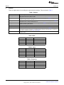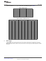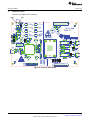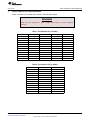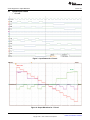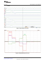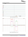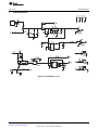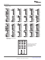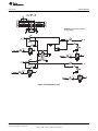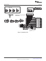
1
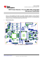
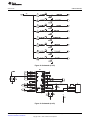
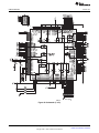
TX517 Dual Channel, 17-Level With RTZ,
Integrated Ultrasound Transmitter
User's Guide
Literature Number: SLOU317B
August 2011 – Revised December 2011
2
SLOU317B – August 2011 – Revised December 2011
Submit Documentation Feedback
Copyright © 2011, Texas Instruments Incorporated
Contents
1
2
3
4
5
Default Configuration .......................................................................................................... 9
Buttons ............................................................................................................................ 10
SYNC Trigger .................................................................................................................... 11
Power up TX517 ................................................................................................................ 12
Power Supplies for Output Waveform .................................................................................. 13
6
7
8
9
...................................................................................................
Board Configuration ..........................................................................................................
EVM Schematics ...............................................................................................................
Bill of Materials .................................................................................................................
PCB Layouts .....................................................................................................................
5.1
Input/Output Pattern
SLOU317B – August 2011 – Revised December 2011
Submit Documentation Feedback
Copyright © 2011, Texas Instruments Incorporated
Table of Contents
14
20
21
28
31
3
www.ti.com
List of Figures
1
Tx517 EVM Basic Configuration .......................................................................................... 9
2
Power-Up Indications ..................................................................................................... 12
3
Input Pattern for 17-Level ................................................................................................ 14
4
Output Waveform for 17-Level ........................................................................................... 14
5
Input Pattern for 5-Level
6
7
8
9
10
11
12
13
14
15
16
17
18
19
20
21
4
.................................................................................................
Output Waveform for 5-Level ...........................................................................................
Input Pattern for 3-Level .................................................................................................
Output Waveform for 3-Level ...........................................................................................
Output Waveform for 2-Level ............................................................................................
Output Waveform for 2-Level With Three Cycles .....................................................................
Output Waveform for 4-Level ............................................................................................
Output Waveform for 32-Level ...........................................................................................
Output Waveform for 32-Level With Two Cycles ......................................................................
Schematic (1 of 8) .........................................................................................................
Schematic (2 of 8) .........................................................................................................
Schematic (3 of 8) .........................................................................................................
Schematic (4 of 8) .........................................................................................................
Schematic (5 of 8) .........................................................................................................
Schematic (6 of 8) .........................................................................................................
Schematic (7 of 8) .........................................................................................................
Schematic (8 of 8) .........................................................................................................
List of Figures
15
15
16
16
17
17
18
18
19
21
22
23
24
25
25
26
27
SLOU317B – August 2011 – Revised December 2011
Submit Documentation Feedback
Copyright © 2011, Texas Instruments Incorporated
www.ti.com
List of Tables
1
Buttons ...................................................................................................................... 10
2
PRF.......................................................................................................................... 10
3
Cycle ........................................................................................................................ 10
4
Frequency .................................................................................................................. 10
5
Pattern Depth .............................................................................................................. 11
6
Patterns of Different Level................................................................................................ 11
7
Pin Definition for J1-Header .............................................................................................. 13
8
Pin Definition for P1-Header ............................................................................................. 13
9
Input/Output, Power, and USB
10
LED Indicators ............................................................................................................. 20
11
Bill of Materials (BOM) .................................................................................................... 28
..........................................................................................
SLOU317B – August 2011 – Revised December 2011
Submit Documentation Feedback
Copyright © 2011, Texas Instruments Incorporated
List of Tables
20
5
6
List of Tables
SLOU317B – August 2011 – Revised December 2011
Submit Documentation Feedback
Copyright © 2011, Texas Instruments Incorporated
www.ti.com
General Texas Instruments High Voltage Evaluation (TI HV EVM) User Safety Guidelines
General Texas Instruments High Voltage Evaluation (TI HV EVM) User Safety Guidelines
WARNING
Always follow TI’s set-up and application instructions, including use of all interface components within their
recommended electrical rated voltage and power limits. Always use electrical safety precautions to help
ensure your personal safety and those working around you. Contact TI’s Product Information Center
http://support/ti./com for further information.
Save all warnings and instructions for future reference.
Failure to follow warnings and instructions may result in personal injury, property damage or
death due to electrical shock and burn hazards.
The term TI HV EVM refers to an electronic device typically provided as an open framed, unenclosed
printed circuit board assembly. It is intended strictly for use in development laboratory environments,
solely for qualified professional users having training, expertise and knowledge of electrical safety risks in
development and application of high voltage electrical circuits. Any other use and/or application are strictly
prohibited by Texas Instruments. If you are not suitable qualified, you should immediately stop from further
use of the HV EVM.
1. Work Area Safety:
(a) Keep work area clean and orderly.
(b) Qualified observer(s) must be present anytime circuits are energized.
(c) Effective barriers and signage must be present in the area where the TI HV EVM and its interface
electronics are energized, indicating operation of accessible high voltages may be present, for the
purpose of protecting inadvertent access I
(d) All interface circuits, power supplies, evaluation modules, instruments, meters, scopes and other
related apparatus used in a development environment exceeding 50Vrms/75VDC must be
electrically located within a protected Emergency Power Off EPO protected power strip.
(e) Use stable and non conductive work surface.
(f) Use adequately insulated clamps and wires to attach measurement probes and instruments. No
freehand testing whenever possible.
2. Electrical Safety:
As a precautionary measure, it is always a good engineering practice to assume that the entire
EVM may have fully accessible and active high voltages.
(a) De-energize the TI HV EVM and all its inputs, outputs and electrical loads before performing any
electrical or other diagnostic measurements. Revalidate that TI HV EVM power has been safely
de-energized.
(b) With the EVM confirmed de-energized, proceed with required electrical circuit configurations, wiring,
measurement equipment hook-ups and other application needs, while still assuming the EVM circuit
and measuring instruments are electrically live.
(c) Once EVM readiness is complete, energize the EVM as intended.
WARNING
While the EVM is energized, never touch the EVM or its electrical
circuits as they could be at high voltages capable of causing
electrical shock hazard.
3. Personal Safety:
(a) Wear personal protective equipment e.g. latex gloves or safety glasses with side shields or protect
EVM in an adequate lucent plastic box with interlocks from accidental touch.
Limitation for safe use: EVMs are not to be used as all or part of a production unit.
SLOU317B – August 2011 – Revised December 2011
Submit Documentation Feedback
Copyright © 2011, Texas Instruments Incorporated
List of Tables
7
8
List of Tables
SLOU317B – August 2011 – Revised December 2011
Submit Documentation Feedback
Copyright © 2011, Texas Instruments Incorporated
User's Guide
SLOU317B – August 2011 – Revised December 2011
TX517 Dual Channel, 17-Level With RTZ, Integrated
Ultrasound Transmitter
TX517 is a fully integrated, dual channel, high voltage Transmitter designed by Texas Instruments
Incorporated. This EVM provides a means to evaluate the functionality of the device. The EVM includes a
FPGA to provide an embedded pattern generator and digital control of the device. The output pattern and
configuration settings are controlled by 8 push buttons on the EVM.
1
Default Configuration
Figure 1. Tx517 EVM Basic Configuration
SLOU317B – August 2011 – Revised December 2011
Submit Documentation Feedback
TX517 Dual Channel, 17-Level With RTZ, Integrated Ultrasound Transmitter
Copyright © 2011, Texas Instruments Incorporated
9
Buttons
2
www.ti.com
Buttons
There are eight buttons for controlling the output waveform settings. They are listed in Table 1.
Table 1. Buttons
Button
Functionality
PHASE_BUTTON
Each time the button is pressed, the current INPx pattern becomes the pattern for INNx, the current
INNx pattern becomes the pattern for INPx.
PRF_BUTTON
Changes the Pulse Repetition Frequency of the output waveform as given in Table 2 Each press
increases the PRF and then cycles back to 0.
CYCLE_BUTTON
Changes the number of times the output pattern cycles within the pulse burst, as given in the Table 3.
Each press moves 1 level up and then back to 0
FREQ_BUTTON
Changes the Frequency of the output waveform as given in the Table 4. Each press increases the
frequency and then cycles back to 0
RESET_BUTTON
Reset all the setting to its default
PDM_BUTTON
One press changes the mode to Power down mode.
CW_MODE_BUTTON
First six times the button is pressed will change the pattern depth as shown in Table 5. Seventh press
will change the device to CW mode. In CW mode, pressing the button will revert back to 17-level. The
latch mode is unaffected. Refer to Table 5 and Table 6.
LATCH_MODE_BUTTON First press changes to latch mode. Every consecutive pulse will toggle the mode between Latch and
Non latch mode
Table 2. PRF
Index
PRF(kHz)
0
0.5
1
1
Comments
2
5
17-level Ramp Only
3
10
17-level Ramp Only
Table 3. Cycle
Index
PRF (kHz)
Comments
0
1
Longer than 5-level Only
1
2
Longer than 5-level Only
2
3
3
5
4
10
Table 4. Frequency
10
Index
Frequency (MHz)
0
10
1
20
2
50
3
100
TX517 Dual Channel, 17-Level With RTZ, Integrated Ultrasound Transmitter
Comments
SLOU317B – August 2011 – Revised December 2011
Submit Documentation Feedback
Copyright © 2011, Texas Instruments Incorporated
SYNC Trigger
www.ti.com
There are 7 patterns: 17-, 5-, 3-, 32-, 4- and 2-level. The patterns are given in Table 6.
Table 5. Pattern Depth
Index
Pattern Depth
0
17
1
5
2
3
3
32
4
4
5
2
6
CW
Comments
Table 6. Patterns of Different Level
17 level
3
5 level
3 level
S/N
Pattern
Level
S/N
Pattern
S/N
Pattern
1
516
8
1
516
8
1
516
2
514
7
2
1026
4
2
2145
0
3
577
6
3
2145
0
3
264
–8
4
1028
5
4
144
–4
5
1026
4
5
264
–8
6
1089
3
7
2084
2
8
2082
1
9
2145
0
10
81
–1
11
73
–2
12
2208
–3
13
144
–4
14
136
–5
15
2336
–6
16
272
–7
17
264
–8
8
SYNC Trigger
A Sync trigger pulse is generated at the start of the pattern transmission for triggering the monitoring
device. Sync pulse will be 5 pattern clock cycle wide and it is active high. Sync pulse output thru J8 SMA
connector..
SLOU317B – August 2011 – Revised December 2011
Submit Documentation Feedback
TX517 Dual Channel, 17-Level With RTZ, Integrated Ultrasound Transmitter
Copyright © 2011, Texas Instruments Incorporated
11
Power up TX517
4
www.ti.com
Power up TX517
Connect +5V adaptor to P2 connector.
+5VDC
GND
Figure 2. Power-Up Indications
12
TX517 Dual Channel, 17-Level With RTZ, Integrated Ultrasound Transmitter
SLOU317B – August 2011 – Revised December 2011
Submit Documentation Feedback
Copyright © 2011, Texas Instruments Incorporated
Power Supplies for Output Waveform
www.ti.com
5
Power Supplies for Output Waveform
Either J1-Header or P1-Header but not both, is used for this purpose.
WARNING
User may be exposed to high voltage depending on power supplies
setting !
Table 7. Pin Definition for J1-Header
Pin
(1)
Voltage
(1)
Pin
Voltage
COMMENT
1
GND
2
OPEN
FB5V
3
GND
4
+5 V
VDD
5
GND
6
–5 V
VEE
7
GND
8
+1.9 V
HV0
9
GND
10
-1.9 V
LV0
11
GND
12
+11 V
VCW
13
GND
14
OPEN
OPEN
15
GND
16
+2.5 V
VAA
17
GND
18
+61 V
HV1
19
GND
20
–20.9 V
LV1
21
GND
22
+32 V
HV2
23
GND
24
–11.9 V
LV2
Use a GND test point for ground
Table 8. Pin Definition for P1-Header
Pin
Voltage
COMMENT
1
OPEN
FB5V
2
+5 V
VDD
3
-5 V
VEE
4
+1.9 V
HV0
5
–1.9 V
LV0
6
+11 V
VCW
7
OPEN
OPEN
8
+2.5 V
VAA
HV1
9
+61 V
10
–20.9 V
LV1
11
+32 V
HV2
12
–11.9 V
LV2
SLOU317B – August 2011 – Revised December 2011
Submit Documentation Feedback
TX517 Dual Channel, 17-Level With RTZ, Integrated Ultrasound Transmitter
Copyright © 2011, Texas Instruments Incorporated
13
Power Supplies for Output Waveform
5.1
www.ti.com
Input/Output Pattern
•
17 Level
Figure 3. Input Pattern for 17-Level
Differential
OUTB
OUTA
Figure 4. Output Waveform for 17-Level
14
TX517 Dual Channel, 17-Level With RTZ, Integrated Ultrasound Transmitter
SLOU317B – August 2011 – Revised December 2011
Submit Documentation Feedback
Copyright © 2011, Texas Instruments Incorporated
Power Supplies for Output Waveform
www.ti.com
•
5 Level
Figure 5. Input Pattern for 5-Level
Differential
OUTB
OUTA
Figure 6. Output Waveform for 5-Level
SLOU317B – August 2011 – Revised December 2011
Submit Documentation Feedback
TX517 Dual Channel, 17-Level With RTZ, Integrated Ultrasound Transmitter
Copyright © 2011, Texas Instruments Incorporated
15
Power Supplies for Output Waveform
•
www.ti.com
3 Level
Figure 7. Input Pattern for 3-Level
Differential
OUTB
OUTA
Figure 8. Output Waveform for 3-Level
16
TX517 Dual Channel, 17-Level With RTZ, Integrated Ultrasound Transmitter
SLOU317B – August 2011 – Revised December 2011
Submit Documentation Feedback
Copyright © 2011, Texas Instruments Incorporated
Power Supplies for Output Waveform
www.ti.com
Figure 9. Output Waveform for 2-Level
Figure 10. Output Waveform for 2-Level With Three Cycles
SLOU317B – August 2011 – Revised December 2011
Submit Documentation Feedback
TX517 Dual Channel, 17-Level With RTZ, Integrated Ultrasound Transmitter
Copyright © 2011, Texas Instruments Incorporated
17
Power Supplies for Output Waveform
www.ti.com
Figure 11. Output Waveform for 4-Level
Figure 12. Output Waveform for 32-Level
18
TX517 Dual Channel, 17-Level With RTZ, Integrated Ultrasound Transmitter
SLOU317B – August 2011 – Revised December 2011
Submit Documentation Feedback
Copyright © 2011, Texas Instruments Incorporated
Power Supplies for Output Waveform
www.ti.com
Figure 13. Output Waveform for 32-Level With Two Cycles
SLOU317B – August 2011 – Revised December 2011
Submit Documentation Feedback
TX517 Dual Channel, 17-Level With RTZ, Integrated Ultrasound Transmitter
Copyright © 2011, Texas Instruments Incorporated
19
Board Configuration
6
www.ti.com
Board Configuration
Table 9. Input/Output, Power, and USB
Connector
Description
P1
External power supplies to the device
P2
+5V power supply connector.
TP5V, TEST_GND
Test points for +5V power supply.
JP20
Jumper to select +5V or FB_5V.
JP21
Select +3.3V.
JP26
Select +1.2V
JP32
External clock/On board OSC
TP1,TP2,TP3,TP4
Ground test points.
TP33V, TP12V
Test points for +3.3V and +1.2V respectively.
JP16
Short always
JP17
Short always
JP18
Short always
JP19
Short always
JP22
Default setup is to output directly/ Others is to drive thru on board transformer.
JP25
JP25: Default setup is to output directly/ Others is to drive thru on board transformer.
JP23
Open when output directly. Short when driving thru transformer
JP24
Short always
JP27
Open
JP29
Open
JP1..JP13
Test points for test pattern. They can also be used for external test patterns.
JP30/JP31
CWINA/CWINB selection.
J6
USB interface connector
Table 10. LED Indicators
20
Reference Designator
Power Supply
LED1/LED2
USB interface indication
LED3/LED7
FPGA alive
LED4
+5V
LED5
+3.3V
LED6
+1.2V
TX517 Dual Channel, 17-Level With RTZ, Integrated Ultrasound Transmitter
SLOU317B – August 2011 – Revised December 2011
Submit Documentation Feedback
Copyright © 2011, Texas Instruments Incorporated
EVM Schematics
www.ti.com
7
EVM Schematics
IN
IN
OUT
EN
GND NR/FB
OUT
GND
EN
NR/FB
Figure 14. Schematic (1 of 8)
SLOU317B – August 2011 – Revised December 2011
Submit Documentation Feedback
TX517 Dual Channel, 17-Level With RTZ, Integrated Ultrasound Transmitter
Copyright © 2011, Texas Instruments Incorporated
21
EVM Schematics
www.ti.com
SOCKET or TX517
WARNING: Users may be exposed
to high voltage
These resistors are not installed.
They are required when an
external generator is used for
pattern generation.
Figure 15. Schematic (2 of 8)
22
TX517 Dual Channel, 17-Level With RTZ, Integrated Ultrasound Transmitter
SLOU317B – August 2011 – Revised December 2011
Submit Documentation Feedback
Copyright © 2011, Texas Instruments Incorporated
EVM Schematics
www.ti.com
VCC
WARNING: Users may be exposed
to high voltage
GND
PURE GREEN
PURE GREEN
PURE GREEN
PURE GREEN
Figure 16. Schematic (3 of 8)
SLOU317B – August 2011 – Revised December 2011
Submit Documentation Feedback
TX517 Dual Channel, 17-Level With RTZ, Integrated Ultrasound Transmitter
Copyright © 2011, Texas Instruments Incorporated
23
EVM Schematics
www.ti.com
WARNING: Users may be exposed
to high voltage
NOTE: D2 and D3 are for internal test.
Do not install
Figure 17. Schematic (4 of 8)
24
TX517 Dual Channel, 17-Level With RTZ, Integrated Ultrasound Transmitter
SLOU317B – August 2011 – Revised December 2011
Submit Documentation Feedback
Copyright © 2011, Texas Instruments Incorporated
EVM Schematics
www.ti.com
Figure 18. Schematic (5 of 8)
Figure 19. Schematic (6 of 8)
SLOU317B – August 2011 – Revised December 2011
Submit Documentation Feedback
TX517 Dual Channel, 17-Level With RTZ, Integrated Ultrasound Transmitter
Copyright © 2011, Texas Instruments Incorporated
25
EVM Schematics
www.ti.com
Figure 20. Schematic (7 of 8)
26
TX517 Dual Channel, 17-Level With RTZ, Integrated Ultrasound Transmitter
SLOU317B – August 2011 – Revised December 2011
Submit Documentation Feedback
Copyright © 2011, Texas Instruments Incorporated
EVM Schematics
www.ti.com
In real application, low-jitter clock should be used on
PCLKIN pin. Typically a main crystal clock; or, through
a jitter cleaner in the system.
VccB
VccA
DIR
GND
B
VccB
VccA
DIR
GND
B
1CLK
A
1Q
1CLR
1Q
VCC
GND
2CLR
2D
2CLK
A
1PRE
1D
2Q
2Q
2PRE
Figure 21. Schematic (8 of 8)
spacer
SLOU317B – August 2011 – Revised December 2011
Submit Documentation Feedback
TX517 Dual Channel, 17-Level With RTZ, Integrated Ultrasound Transmitter
Copyright © 2011, Texas Instruments Incorporated
27
Bill of Materials
8
www.ti.com
Bill of Materials
Table 11. Bill of Materials (BOM)
QTY
28
MFG
MFG PART#
RefDes
Description
Value or Function
1
TX517
TX517
U20
Ultrasound Transmitter
TX517 transmitter ( TI Provide)
2
PANASONIC
EEUFC2A101L
C72, C73
CAP,RAD,ELEC
CAP,THRU,ELE,100uf,100V,20%
16
AVX
0402YC103KAT2A
C10, C12, C14, C16, C18, C20,
C22, C24, C26, C28, C30, C32,
C33, C35, C37, C39
CAP,SMT,0402
CAPACITOR,SMT,0402,CERAMIC,10000pF,16V,10%,X7R
13
AVX
0402YC104KAT2A
C43, C60, C61, C63, C66, C68,
C69, C70, C71, C75, C76, C90, C91
CAP,SMT,0402
CAPACITOR,SMT,0402,CER,16V,10%,0.1uF
31
KEMET
C0402C104K8PAC
C2, C3, C5, C6, C9, C11, C13, C15,
C17, C19, C21, C23, C25, C27,
C29, C31, C34, C36, C38, C40,
C48, C62, C67, C78, C79, C80,
C83, C84, C85, C86, C87
CAP,SMT,0402
CAPACITOR,SMT,0402,CER,0.1uF,10V,10%,X5R
1
PANASONIC
ECJ-0EB1H102K
C8
CAP,SMT,0402
CAPACITOR,SMT,0402,CER,1000pF,50V,10%,X7R
2
PANASONIC
ECJ-0EC1H470J
C81, C82
CAP,SMT,0402
CAPACITOR,SMT,0402,CER,47pF,50V,5%,NPO
2
AVX
06033C104JAT2A
C64, C65
CAP,SMT,0603
CAPACITOR,SMT,0603,CERAMIC,0.1uF,25V,5%,X7R
1
CAPAX
0603X475J250SW
C52
CAP,SMT,0603
CAPACITOR,SMT,0603,CERAMIC,4.7uF,25V,5%,X7R
1
TAIYO YUDEN
JMK107BJ106MA-T
C7
CAP,SMT,0603
CAPACITOR,SMT,0603,CERAMIC,10uF,6.3V,20%,X5R
5
TAIYO YUDEN
LMK107BJ475KA-T
C53, C54, C55, C92, C93
CAP,SMT,0603
CAPACITOR,SMT,0603,CERAMIC,4.7uF,10V,10%,X5R
8
AVX
08051C104KAZ2A
C41, C42, C49, C50, C56, C57,
C58, C59
CAP,SMT,0805
CAPACITOR,SMT,0805,CERAMIC,0.1uF,100V,10%
4
TAIYO YUDEN
HMK325BJ225KN
C44, C45, C46, C51
CAP,SMT,1210
CAPACITOR,SMT,1210,CERAMIC,2.2uF,100V,10%,X7R
2
VISHAY
593D226X9016C2T
C1, C4
CAP,SMT,TANT
CAP,TAN,SMT,EIA-C,16V,10%, 22uF
1
AVX
TPSC226K016R0375
C47
CAPACITOR,SMT,TANT
10%, 16V, 22uF
2
JOHNSON COMPONENTS
142-0711-826
J2, J3
CON,SMA,SMT
SMA JACK,END LAUNCH,A068,062PCB,BRASS/NICKEL
1
ADVANCED CONNECTEK
MNE20-5K5P10
J6
CONN,SMT,5P
MINI-AB USB OTG RECEPTACLE R/A SMT TYPE
4
AMPHENOL
901-144-8
J8, J9, J11, J29
CONNECTOR,SMA
SMA COAX STRAIGHT PCB CURRENT P/N IS 901-144-8RFX
1
Customer Supply
DO NOT INSTALL
T1
Transformer
Do Not Install
4
DIODES INC.
1N4148W-7
CR1, CR2, CR3, CR4
DIODE,SMT,2P
DIODE,SMT,SWITCHING,1N4148
1
DIODES INC.
MMBD3004S-7-F
D1
DIODE,SMT,3P
DIODE SWITCH 300V 350MW SOT23-3
5
STEWARD
HI0805R800R-00
L1, L2, L3, L4, L5
FERRITE BEAD,SMT,2P
1
SAMTEC
IPL-112-01-S-D-K
J1
HEADER,THP,24P
HEADER,THP,24P,MALE,2X12,100LS,.120TL
1
MOLEX
39357-0002
P2
HEADER,THRU,2P
HEADER, THRU, POWER, 2P,3.5MM, EUROSTYLE
1
SPC TECH
8431-1x12 (DNI)
P1
HEADER,THU,12P
HEADER,THU,MALE,0.1LS,12P,1X12,335H,120TL,(Do Not
Install)
1
MOLEX
87831-1420
J10
HEADER,THU,14P
HEADER,MALE,14POS,2 ROWS,2mm LS,15u,LF,TL=098
2
SPC TECH
8431-1x9
J28A, J28B
HEADER,THU,9P
HEADER,THU,MALE,0.1LS,9P,1X9,335H,120TL
TX517 Dual Channel, 17-Level With RTZ, Integrated Ultrasound Transmitter
Copyright © 2011, Texas Instruments Incorporated
SLOU317B – August 2011 – Revised December 2011
Submit Documentation Feedback
Bill of Materials
www.ti.com
Table 11. Bill of Materials (BOM) (continued)
QTY
MFG
MFG PART#
RefDes
Description
Value or Function
21
TYCO ELECTRONICS
4-103239-0x2
JP1, JP2, JP3, JP4, JP5, JP6, JP7,
JP8, JP9, JP10, JP11, JP12, JP13,
JP16, JP17, JP18, JP19, JP23,
JP24, JP27, JP29
HEADER,THU,JUMPER
MALE,2PIN,.100CC MAKE FROM 4-103239-0x2
8
TYCO ELECTRONICS
4-103239-0x3
JP20, JP21, JP22, JP25, JP26,
JP30, JP31,JP32
HEADER,THU,JUMPER
MAKE FROM 4-103239-0
2
TI
SN74LVC1T45DCKR
U4, U6
IC,SMT,6P
SINGLE BIT DUAL SUPPLY BUS TRANSCEIVER
1
TI
SN74HC04D
U7
IC,SMT,SOIC-14N
HEX INVERTER
1
TI
TPS79633DCQR
U1
IC,SMT,SOT223-6
ULTRALOW-NOISE HI PSRR FAST RF 1-A LDO LINEAR
REGULATOR,3.3V
1
TI
TPS73201QDBV
U2
IC,SMT,SOT23-5
CAP-FREE NMOS 250-mA LOW DROPOUT REGULATOR
1
FUTURE TECHNOLOGY DEVICE
INT.
FT245RL
U5
IC,SMT,SSOP-28
USB FIFO IC INCORPORATE FTDICHIP-ID SECURITY
DONGLE
1
XILINX
XC3S50AN-4TQG144I
U3
IC,SMT,TQFP-144
XILINX SPARTAN-3AN 144QFP
1
TI
74AC11074PW
U8
IC,SMT,TSSOP-14
DUAL POS-EDGE-TRIG D-TYPE FLIP-FLOP W CLEAR AND
PRESET,PW-14
1
TI
CDCLVC1102PWR
U9
IC,SMT,TSSOP-8
3.3V AND 2.5V LVCMOS HIGH PERF CLOCK BUFFER FAMILY
7
PANASONIC
LNJ308G8PRA
LED4, LED5, LED6, LED8, LED9,
LED10, LED11
LED,SMT,0603
LED,SMT,0603,PURE GREEN,2.03V
4
KINGBRIGHT
KP-2012ID
LED1, LED2, LED3, LED7
LED,SMT,2P
LED,RED,SMT,0805
1
ECS
ECS-3953M-1000-BN
OSC1
OSCILLATOR,SMT,4P
OSC,SMT,3.3V,50ppm,-40~85C,5nS,100.000 MHz
2
*COTO TECHNOLOGY
9402-05-20
Y3, Y4
RELAY,SMT,6P
SPST,SMT,50 OHM,5V,0.5A,200 OHM COIL,J-LEAD (Not
Install)
2
*COTO TECHNOLOGY
2911-05-321
Y1, Y2
RELAY,THRU,7P
RELAY,THRU,7P,RR,SPDT,1FC,5V,0.25A,230R COIL,COAXIAL
SHIELD (Not Install)
15
PANASONIC
ERJ-2RKF1001X
R6, R7, R8, R9, R10, R11, R12,
R21, R22, R23, R24, R25, R26,
R28, R30
RES,SMT,0402
RESISTOR,SMT,0402,1.00K,1%,1/16W
8
PANASONIC
ERJ-2RKF1002X
R13, R14, R15, R16, R17, R18,
R19, R29
RES,SMT,0402
RESISTOR,SMT,0402,10.0K,1%,1/16W
7
PANASONIC
ERJ-2RKF3320X
R1, R2, R3, R45, R46, R47, R50
RES,SMT,0402
RESISTOR,SMT,0402,332 OHM,1%,1/16W
2
PANASONIC
ERJ-2RKF49R9X
R20, R52
RES,SMT,0402
RESISTOR,SMT,0402,49.9 OHM,1%,1/16W,
2
VISHAY
CRCW08051002F
R48, R49
RES,SMT,0805
RESISTOR,SMT,0805,THICK FILM,1%,1/8W,10.0K
2
VISHAY
CRCW251249R9FKEG
R4, R5
RESISTOR,SMT,2512
RESISTOR,SMT,2512,THICK FILM,49.9 OHM,1%,1W
8
ITT INDUSTRIES
PTS635SK25SM
SW1, SW2, SW3, SW4, SW5, SW6,
SW7, SW8
SWITCH,SMT,2P
SWITCH,SMT,2P,SPST-NO,2.5mm
HEIGHT,MOM,RECTANGULAR,0.05A,12V
3
KEYSTONE ELECTRONICS
5000
TP12V, TP33V, TP5V
TESTPOINT,THU,1P
TESTPOINT,THU,MINIATURE,0.1LS,120TL, RED
5
KEYSTONE ELECTRONICS
5001
TP1, TP2, TP3, TP4, TEST_GND
TESTPOINT,THU,1P
TESTPOINT,THU,MINIATURE,0.1LS,120TL, BLACK
2
ON SEMI
1SMA5927BT3
D2, D3
ZENER DIODE,SMT,SMA
ZENER DIODE,12V,SMT,SMA,1.5W (Not Installed)
1
ON SEMI
1SMB5920BT3
Z1
ZENER DIODE,SMT,SMB
ZENER DIODE,6.2V,SMT,SMB,3W
2
TYCO
50935
Y1, Y2
SOCKET PIN - INSTALL 1ST
DIA_038, PIN_013-020, EXP_146, B125
SLOU317B – August 2011 – Revised December 2011
Submit Documentation Feedback
TX517 Dual Channel, 17-Level With RTZ, Integrated Ultrasound Transmitter
Copyright © 2011, Texas Instruments Incorporated
29
Bill of Materials
www.ti.com
Table 11. Bill of Materials (BOM) (continued)
QTY
MFG
MFG PART#
RefDes
Description
Value or Function
1
PANASONIC
ERJ-2RKF49R9X
R27
RES,SMT,0402
RESISTOR,SMT,0402,49.9 OHM,1%,1/16W(Not Install)
1
Customer Supply
DO NOT INSTALL
T1B
Transformer
DO NOT INSTALL
15
PANASONIC
ERJ-2RKF49R9X(DNI)
R31, R32, R33, R34, R35, R36,
R37, R38, R39, R40, R41, R42,
R43, R44, R51
RES,SMT,0402
RESISTOR,SMT,0402,49.9 OHM,1%,1/16W, Uninstall
4
KEYSTONE ELECTRONICS
24436K-ND
STANDOFF HEX M3 THR
ALUM 18MM
STANDOFF HEX M3 THR ALUM 18MM
4
KEYSTONE ELECTRONICS
29311K-ND
SCREW STEEL M3 THR
6MM
SCREW STEEL M3 THR 6MM
TE Connectivity
1658621-5
Cover for P1
Snap latch into place. Install as needed
SPECIAL NOTES AND INSTRUCTIONS
30
TX517 Dual Channel, 17-Level With RTZ, Integrated Ultrasound Transmitter
Copyright © 2011, Texas Instruments Incorporated
SLOU317B – August 2011 – Revised December 2011
Submit Documentation Feedback
PCB Layouts
www.ti.com
9
PCB Layouts
SLOU317B – August 2011 – Revised December 2011
Submit Documentation Feedback
TX517 Dual Channel, 17-Level With RTZ, Integrated Ultrasound Transmitter
Copyright © 2011, Texas Instruments Incorporated
31
PCB Layouts
32
www.ti.com
TX517 Dual Channel, 17-Level With RTZ, Integrated Ultrasound Transmitter
SLOU317B – August 2011 – Revised December 2011
Submit Documentation Feedback
Copyright © 2011, Texas Instruments Incorporated
PCB Layouts
www.ti.com
SLOU317B – August 2011 – Revised December 2011
Submit Documentation Feedback
TX517 Dual Channel, 17-Level With RTZ, Integrated Ultrasound Transmitter
Copyright © 2011, Texas Instruments Incorporated
33
Evaluation Board/Kit Important Notice
Texas Instruments (TI) provides the enclosed product(s) under the following conditions:
This evaluation board/kit is intended for use for ENGINEERING DEVELOPMENT, DEMONSTRATION, OR EVALUATION
PURPOSES ONLY and is not considered by TI to be a finished end-product fit for general consumer use. Persons handling the
product(s) must have electronics training and observe good engineering practice standards. As such, the goods being provided are
not intended to be complete in terms of required design-, marketing-, and/or manufacturing-related protective considerations,
including product safety and environmental measures typically found in end products that incorporate such semiconductor
components or circuit boards. This evaluation board/kit does not fall within the scope of the European Union directives regarding
electromagnetic compatibility, restricted substances (RoHS), recycling (WEEE), FCC, CE or UL, and therefore may not meet the
technical requirements of these directives or other related directives.
Should this evaluation board/kit not meet the specifications indicated in the User’s Guide, the board/kit may be returned within 30
days from the date of delivery for a full refund. THE FOREGOING WARRANTY IS THE EXCLUSIVE WARRANTY MADE BY
SELLER TO BUYER AND IS IN LIEU OF ALL OTHER WARRANTIES, EXPRESSED, IMPLIED, OR STATUTORY, INCLUDING
ANY WARRANTY OF MERCHANTABILITY OR FITNESS FOR ANY PARTICULAR PURPOSE.
The user assumes all responsibility and liability for proper and safe handling of the goods. Further, the user indemnifies TI from all
claims arising from the handling or use of the goods. Due to the open construction of the product, it is the user’s responsibility to
take any and all appropriate precautions with regard to electrostatic discharge.
EXCEPT TO THE EXTENT OF THE INDEMNITY SET FORTH ABOVE, NEITHER PARTY SHALL BE LIABLE TO THE OTHER
FOR ANY INDIRECT, SPECIAL, INCIDENTAL, OR CONSEQUENTIAL DAMAGES.
TI currently deals with a variety of customers for products, and therefore our arrangement with the user is not exclusive.
TI assumes no liability for applications assistance, customer product design, software performance, or infringement of
patents or services described herein.
Please read the User’s Guide and, specifically, the Warnings and Restrictions notice in the User’s Guide prior to handling the
product. This notice contains important safety information about temperatures and voltages. For additional information on TI’s
environmental and/or safety programs, please contact the TI application engineer or visit www.ti.com/esh.
No license is granted under any patent right or other intellectual property right of TI covering or relating to any machine, process, or
combination in which such TI products or services might be or are used.
FCC Warning
This evaluation board/kit is intended for use for ENGINEERING DEVELOPMENT, DEMONSTRATION, OR EVALUATION
PURPOSES ONLY and is not considered by TI to be a finished end-product fit for general consumer use. It generates, uses, and
can radiate radio frequency energy and has not been tested for compliance with the limits of computing devices pursuant to part 15
of FCC rules, which are designed to provide reasonable protection against radio frequency interference. Operation of this
equipment in other environments may cause interference with radio communications, in which case the user at his own expense
will be required to take whatever measures may be required to correct this interference.
EVM Warnings and Restrictions
It is important to operate this EVM within the input voltage range of –0.3 V to 5.3 V and the output voltage range of –0.3 V to 3.3 V
.
Exceeding the specified input range may cause unexpected operation and/or irreversible damage to the EVM. If there are
questions concerning the input range, please contact a TI field representative prior to connecting the input power.
Applying loads outside of the specified output range may result in unintended operation and/or possible permanent damage to the
EVM. Please consult the EVM User's Guide prior to connecting any load to the EVM output. If there is uncertainty as to the load
specification, please contact a TI field representative.
During normal operation, some circuit components may have case temperatures greater than 50°C. The EVM is designed to
operate properly with certain components above 25°C as long as the input and output ranges are maintained. These components
include but are not limited to linear regulators, switching transistors, pass transistors, and current sense resistors. These types of
devices can be identified using the EVM schematic located in the EVM User's Guide. When placing measurement probes near
these devices during operation, please be aware that these devices may be very warm to the touch.
Mailing Address: Texas Instruments, Post Office Box 655303, Dallas, Texas 75265
Copyright © 2011, Texas Instruments Incorporated
IMPORTANT NOTICE
Texas Instruments Incorporated and its subsidiaries (TI) reserve the right to make corrections, modifications, enhancements, improvements,
and other changes to its products and services at any time and to discontinue any product or service without notice. Customers should
obtain the latest relevant information before placing orders and should verify that such information is current and complete. All products are
sold subject to TI’s terms and conditions of sale supplied at the time of order acknowledgment.
TI warrants performance of its hardware products to the specifications applicable at the time of sale in accordance with TI’s standard
warranty. Testing and other quality control techniques are used to the extent TI deems necessary to support this warranty. Except where
mandated by government requirements, testing of all parameters of each product is not necessarily performed.
TI assumes no liability for applications assistance or customer product design. Customers are responsible for their products and
applications using TI components. To minimize the risks associated with customer products and applications, customers should provide
adequate design and operating safeguards.
TI does not warrant or represent that any license, either express or implied, is granted under any TI patent right, copyright, mask work right,
or other TI intellectual property right relating to any combination, machine, or process in which TI products or services are used. Information
published by TI regarding third-party products or services does not constitute a license from TI to use such products or services or a
warranty or endorsement thereof. Use of such information may require a license from a third party under the patents or other intellectual
property of the third party, or a license from TI under the patents or other intellectual property of TI.
Reproduction of TI information in TI data books or data sheets is permissible only if reproduction is without alteration and is accompanied
by all associated warranties, conditions, limitations, and notices. Reproduction of this information with alteration is an unfair and deceptive
business practice. TI is not responsible or liable for such altered documentation. Information of third parties may be subject to additional
restrictions.
Resale of TI products or services with statements different from or beyond the parameters stated by TI for that product or service voids all
express and any implied warranties for the associated TI product or service and is an unfair and deceptive business practice. TI is not
responsible or liable for any such statements.
TI products are not authorized for use in safety-critical applications (such as life support) where a failure of the TI product would reasonably
be expected to cause severe personal injury or death, unless officers of the parties have executed an agreement specifically governing
such use. Buyers represent that they have all necessary expertise in the safety and regulatory ramifications of their applications, and
acknowledge and agree that they are solely responsible for all legal, regulatory and safety-related requirements concerning their products
and any use of TI products in such safety-critical applications, notwithstanding any applications-related information or support that may be
provided by TI. Further, Buyers must fully indemnify TI and its representatives against any damages arising out of the use of TI products in
such safety-critical applications.
TI products are neither designed nor intended for use in military/aerospace applications or environments unless the TI products are
specifically designated by TI as military-grade or "enhanced plastic." Only products designated by TI as military-grade meet military
specifications. Buyers acknowledge and agree that any such use of TI products which TI has not designated as military-grade is solely at
the Buyer's risk, and that they are solely responsible for compliance with all legal and regulatory requirements in connection with such use.
TI products are neither designed nor intended for use in automotive applications or environments unless the specific TI products are
designated by TI as compliant with ISO/TS 16949 requirements. Buyers acknowledge and agree that, if they use any non-designated
products in automotive applications, TI will not be responsible for any failure to meet such requirements.
Following are URLs where you can obtain information on other Texas Instruments products and application solutions:
Products
Applications
Audio
www.ti.com/audio
Communications and Telecom www.ti.com/communications
Amplifiers
amplifier.ti.com
Computers and Peripherals
www.ti.com/computers
Data Converters
dataconverter.ti.com
Consumer Electronics
www.ti.com/consumer-apps
DLP® Products
www.dlp.com
Energy and Lighting
www.ti.com/energy
DSP
dsp.ti.com
Industrial
www.ti.com/industrial
Clocks and Timers
www.ti.com/clocks
Medical
www.ti.com/medical
Interface
interface.ti.com
Security
www.ti.com/security
Logic
logic.ti.com
Space, Avionics and Defense
www.ti.com/space-avionics-defense
Power Mgmt
power.ti.com
Transportation and Automotive www.ti.com/automotive
Microcontrollers
microcontroller.ti.com
Video and Imaging
RFID
www.ti-rfid.com
OMAP Mobile Processors
www.ti.com/omap
Wireless Connectivity
www.ti.com/wirelessconnectivity
TI E2E Community Home Page
www.ti.com/video
e2e.ti.com
Mailing Address: Texas Instruments, Post Office Box 655303, Dallas, Texas 75265
Copyright © 2011, Texas Instruments Incorporated