1
US 7,689,815 B2
13
14
Thus, it is to be understood that the architectures depicted
herein are merely exemplary, and that in fact many other
should not be construed to imply that the introduction of
another claim element by the inde?nite articles “a” or “an”
architectures can be implemented Which achieve the same
functionality. In an abstract, but still de?nite sense, any
arrangement of components to achieve the same functionality
element to inventions containing only one such element, even
When the same claim includes the introductory phrases “one
limits any particular claim containing such introduced claim
is effectively “associated” such that the desired functionality
or more” or “at least one” and inde?nite articles such as “a” or
“an.” The same holds true for the use of de?nite articles.
is achieved. Hence, any tWo components herein combined to
Unless stated otherWise, terms such as “?rst” and “second”
are used to arbitrarily distinguish betWeen the elements such
terms describe. Thus, these terms are not necessarily intended
to indicate temporal or other prioritiZation of such elements.
What is claimed is:
achieve a particular functionality can be seen as “associated
Wit ” each other such that the desired functionality is
achieved, irrespective of architectures or intermedial compo
nents. Likewise, any tWo components so associated can also
be vieWed as being “operably connected,” or “operably
coupled,” to each other to achieve the desired functionality.
Also for example, in one embodiment, the illustrated ele
1. A method, comprising:
providing a ?rst debug instruction;
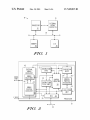
ments of system 10 are circuitry located on a single integrated
providing a ?eld in the ?rst debug instruction to indicate a
circuit or Within a same device. Alternatively, system 10 may
group number;
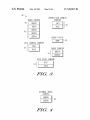
providing a plurality of debug control register ?elds,
include any number of separate integrated circuits or separate
devices interconnected With each other. Also for example,
Wherein the group number associates a ?rst one of the
plurality of debug control register ?elds to the ?rst debug
system 10 or portions thereof may be soft or code represen
tations of physical circuitry or of logical representations con
vertible into physical circuitry. As such, system 10 may be
embodied in a hardWare description language of any appro
20
priate type.
Furthermore, those skilled in the art Will recogniZe that
boundaries betWeen the functionality of the above described
25
operations merely illustrative. The functionality of multiple
operations may be combined into a single operation, and/or
the functionality of a single operation may be distributed in
additional operations. Moreover, alternative embodiments
may include multiple instances of a particular operation, and
the order of operations may be altered in various other
embodiments.
tion; and
providing a second debug instruction, Wherein the second
debug instruction has no ?eld to indicate the group num
30
ber,
Wherein a second one of the plurality of debug control
register ?elds is associated to the second debug instruc
tion,
All or some of the softWare described herein may be
received elements of data processing system 10, for example,
from computer readable media such as memory 18 or other
instruction,
Wherein if the ?rst one of the plurality of debug control
register ?elds has a ?rst value, the ?rst debug instruction
is to be executed as the ?rst debug instruction, and
Wherein if the ?rst one of the plurality of debug control
register ?elds has a second value, the ?rst debug instruc
tion is to be executed as a no-operation (N OP) instruc
Wherein if the second one of the plurality of debug control
35
register ?elds has the ?rst value, the second debug
media on other computer systems. Such computer readable
instruction is to be executed as the second debug instruc
media may be permanently, removably or remotely coupled
tion, and
Wherein if the second one of the plurality of debug control
to an information processing system such as data processing
system 10. The computer readable media may include, for
example and Without limitation, any number of the folloWing:
register ?elds has the second value, the second debug
40
magnetic storage media including disk and tape storage
media; optical storage media such as compact disk media
(e.g., CD-ROM, CD-R, etc.) and digital video disk storage
media; nonvolatile memory storage media including semi
conductor-based memory units such as FLASH memory,
45
EEPROM, EPROM, ROM; ferromagnetic digital memories;
MRAM; volatile storage media including registers, buffers or
caches, main memory, RAM, etc.; and data transmission
media including computer netWorks, point-to-point telecom
munication equipment, and carrier Wave transmission media,
50
just to name a feW.
a processor on an integrated circuit has Write access to the
Although the invention is described herein With reference
debug control register ?elds and the processor on the inte
grated circuit does not have Write access to the debug control
to speci?c embodiments, various modi?cations and changes
can be made Without departing from the scope of the present
invention as set forth in the claims beloW. Accordingly, the
speci?cation and ?gures are to be regarded in an illustrative
register ?elds.
55
plurality of debug control register ?elds and the second one of
intended to be included Within the scope of the present inven
tion. Any bene?ts, advantages, or solutions to problems that
the plurality of debug control register ?elds are a same one of
60
the plurality of debug control register ?elds.
7. A method as in claim 1, Wherein the ?rst one of the
plurality of debug control register ?elds and the second one of
the plurality of debug control register ?elds are different ones
feature or element of any or all the claims.
The term “coupled,” as used herein, is not intended to be
limited to a direct coupling or a mechanical coupling.
Furthermore, the terms “a” or “an,” as used herein, are
5. A method as in claim 1, Wherein the ?rst debug instruc
tion is different than the second debug instruction.
6. A method as in claim 1, Wherein the ?rst one of the
rather than a restrictive sense, and all such modi?cations are
are described herein With regard to speci?c embodiments are
not intended to be construed as a critical, required, or essential
instruction is to be executed as the NOP operation
instruction.
2. A method as in claim 1, Wherein a debugger external to
an integrated circuit has Write access to the debug control
register ?elds and a processor on the integrated circuit does
not have Write access to the debug control register ?elds.
3. A method as in claim 1, Wherein a debugger external to
an integrated circuit does not have Write access to the debug
control register ?elds and a processor on the integrated circuit
does have Write access to the debug control register ?elds.
4. A method as in claim 1, Wherein a debugger external to
of the plurality of debug control register ?elds.
65
8. A method as in claim 1, Wherein if the ?rst one of the
de?ned as one or more than one. Also, the use of introductory
plurality of debug control register ?elds has the ?rst value,
phrases such as “at least one” and “one or more” in the claims
execution of the ?rst debug instruction causes entry into a