1
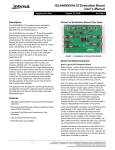
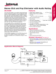
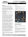
ISL5440XEVAL1Z Evaluation Board
User’s Manual
®
Application Note
July 19, 2006
AN1255.0
Description
Features
The ISL5440XEVAL1Z evaluation board is designed to
provide a quick and easy method for evaluating the
ISL54400, ISL54401 and ISL54402 USB/Audio Switch ICs.
• Dip Socket For Quick Removal and Installation of DUTs
An evaluation kit consists of the following items: One Main
Evaluation Board; Three µTQFN to Dip Daughter Boards
with mounted IC; ISL5440XEVAL1Z Evaluation Board User’s
Manual; ISL54400, ISL54401, ISL54402 Data Sheet; Main
Evaluation Board Schematic.
• Standard USB Connectors
• RCA Audio Input Jacks and Headphone Speaker Jack
• Convenient Test Points and Connections for Test
Equipment
Picture of Evaluation Board (Top View)
The ISL54400EVAL1Z kit contains three daughter boards
with the ISL54400 part.
The ISL54401EVAL1Z kit contains three daughter boards
with the ISL54401 part.
The ISL54402EVAL1Z kit contains three daughter boards
with the ISL54402 part.
The ISL5440x devices are unique ICs. To use this evaluation
platform properly requires thorough knowledge of the operation
of the ICs. Refer to the data sheet for an understanding of the
functions and features of this family of devices. Studying a
device’s truth-table along with its pinout diagram on pages 2
and 3 of the data sheet is the best way to get a quick
understanding of how a particular part in this family works.
A picture of the main evaluation board with IC to dip daughter
board installed is shown in Figure 1. The main board has a 10
pin dip socket (U1) located in the center of the board. An IC is
soldered onto a 10 pin dip daughter board that is plugged into
the dip socket on the main board. Using daughter boards
allow for the easy installation and removal of ICs.
The USB/Audio Switch ICs have two modes of operation
called Audio mode and USB mode. The main evaluation
board contains standard Audio and USB connectors to allow
the user to easily interface with the IC to evaluate its
functions, features, and performance in the two modes of
operation. For example, when the board is properly
powered, a headphone can be plugged into the headphone
jack (J7) and a stereo source, such as a MP3 player, can be
connected at the RCA connectors J3 (AUDIO LEFT) and J4
(AUDIO RIGHT) to play music through the audio switches of
the IC. See Figure 2. You can then turn-off the audio source,
remove the headphones, and attach a USB cable from a
computer to USB connector J1. This will establish a
connection from the computer through the USB switches of
the IC to the USB device, that is connected at the USB
connector J2, to send and receive data.
This application note will guide the user through the process
of configuring and using the evaluation board to evaluate the
ISL5440x family of devices in both the Audio mode and the
USB mode.
1
FIGURE 1. ISL5440XEVAL1 BOARD WITH IC DIP BOARD
INSTALLED
Board Architecture/Layout
Basic Layout of Main Board
The basic layout of the main board is as follows: Refer to
Figure 1.
Power and Ground connections are at the top of the board
(J10 and J11).
Audio Source Inputs are at the lower right side of the board
(J3 - J6). Audio outputs are at the lower left side of the board
(J7, J8, J9). Connector J7 is a standard headphone jack for
connecting a 32Ω headphone.
USB connection to an upstream host controller (Computer)
is made at connector J1, located on left under-side of the
main board. USB connection to a downstream USB device is
made at connector J2, located on right under-side of the
main board.
CAUTION: These devices are sensitive to electrostatic discharge; follow proper IC Handling Procedures.
1-888-INTERSIL or 1-888-468-3774 | Intersil and Design is a trademark of Intersil Americas Inc.
Copyright © Intersil Americas Inc. 2006, All Rights Reserved
Application Note 1255
Located in the center of the board is the DIP socket (U1).
The IC to Dip Daughter Board plugs into this socket. The
main board has a pin 1 label, to show how the IC daughter
board should be oriented in the socket. The daughter board
pin 1 indicator dot needs to be aligned with the main
evaluation board dip socket labeled 1.
Power Supply
The ISL5440x devices require a DC power supply for proper
operation. The DC power supply + and - terminals are
connected at banana jacks J10 (VDD) and J11 (GND)
located at the top of the board.
ISL54400 AND ISL54401
In Audio mode the VDD power supply connected at banana
jacks J10 (VDD) and J11 (GND) provides power to the part.
A 2.7V to 3.6V DC power supply is needed for proper
operation. The power supply should be capable of delivering
100µA of current.
In USB mode the VBUS 5VDC voltage from the host USB
controller (computer) connected at the USB connector J1
(USB to HOST) provides power to the part.
NOTE: For the ISL54400 and ISL54401 devices the VBUS
voltage needs to be at least 0.8V higher than the voltage at
VDD to turn the audio switches OFF and turn the USB
switches ON. In a typical application, the VBUS voltage from
host controller will be in the range of 4.4V to 5.25V and the
VDD voltage will be in the range of 2.7V to 3.6V.
The ISL54400 VTERM does not output a voltage unless
VBUS > VDD + 0.8V and VDD > 2.5V.
ISL54402
Power for the ISL54402 device is always provided by the DC
voltage source connected at the J10 (VDD) and J11 (GND)
Led jacks. The VDD voltage can be in the range of 1.8V to
5.5V. In a USB application, it should be set in the range of
2.7V to 5.5V and should be capable of delivering 100µA of
current.
Logic Control
ISL54400 AND ISL54401
The state of the ISL54400 and ISL54401 devices is
determined by the voltage at the VBUS pin. If VBUS is
floating (no USB host controller connected at the J1
connector) the part will be in the Audio mode.
If VBUS is greater than VDD by 0.8V (USB host controller
connected at the J1 USB connector) the part will be in the
USB mode. In a typical application the VBUS voltage from
host controller will be in the range of 4.4V to 5.25V and the
VDD voltage will be in the range of 2.7V to 3.6V.
ISL54402
Logic control for the ISL54002 device is the same as a
standard dual SPDT switch. The voltage applied at J13 (IN2)
and J12 (IN1) determines whether the NOx (Digital) or NCx
2
(Audio) switches are ON or OFF. The ISL54002 logic levels
are TTL compatible. See truth-table on page 3 of data sheet.
In a typical application, connector J12 and J13 should be
connected together, allowing the logic control inputs to the IC
to work in tandem. If you pull them LOW by connecting them
to ground the NCx switches will be ON. If you pull them
HIGH by connecting them to VDD or VBUS of the computer
(In USB application) the NOx switches will be ON.
NOTE: The BNC connector J13 is wired in parallel with the
VBUS line of the USB J1 connector. When you connect a
USB cable from a computer to the J1 USB connector this will
put the logic of pin 2 (IN2) of the IC at 5V. If connector J12 is
connected to connector J13 then the logic of pin 10 (IN1) of
the IC will also be at 5V and both USB switches will be ON.
This is required for proper USB operation.
Audio Inputs
The evaluation board has two audio inputs labeled AUDIO
LEFT (J3 or J5) and AUDIO RIGHT (J4 or J6). Each of these
inputs have a BNC connector wired in parallel with a RCA
jack connector. You can connect an audio source/generator
at either the BNC connector or the RCA connector.
In a typical application, the left and right outputs of a stereo
source, such as an MP3 player, would be connect to the
RCA jacks J3 and J4, respectfully.
The internal audio switches of the ISL5440x family of
devices were designed to pass a 0.6VRMS signal across a
32Ω headphone load with very low signal distortion. The
audio source amplitude should be less than 1.75Vpp
(0.62Vrms) for best performance. A 3Vpp signal is
acceptable but performance will degrade.
The audio channels are AC coupled with 100µF capacitors.
These caps remove any DC voltage from the audio signals
and reference them to ground of the device.
NOTE: The audio switches are not bi-directional. The audio
source needs to be connected at J3 or J5 and J4 or J6. Do
not try to apply an audio source at the J8 and J9 BNC
connectors on left side of the board and loads at J3 - J6 on
right side of the board.
NOTE: When in USB mode the audio source needs to be in
a high impedance state so it will not interfere with the USB
signal. Since the audio source inputs are AC coupled on the
eval board, simply turning the audio source OFF will isolate it
from interfering with the USB signal.
Audio Outputs
The evaluation board has a standard headphone jack
labeled HEADPHONE JACK (J7). A 32Ω stereo headphone
should be plugged into this jack. The BNC connector J8
(D-/L/COM1) is in parallel with the audio left signal of the
headphone jack. The BNC connector J9 (D+/R/COM2) is in
parallel with the audio right signal of the headphone jack.
These BNC connectors can be used to connect resistive
AN1255.0
July 19, 2006
Application Note 1255
loads and/or test equipment to evaluate the performance of
the IC.
USB Connections
A “B” type USB receptacle labeled USB TO HOST (J1) is
located on the left under-side of the board. This receptacle
should be connected, using a standard USB cable, to the
up-stream USB host controller which is usually a computer.
When this connection is made, an ISL54400 or ISL54401
device will sense the VBUS voltage from the host controller
and go into USB mode. The USB switches will be turned ON
and the IC will get its power from the VBUS line.
VTERM Connection (ISL54400 only)
To use VTERM output of the ISL54400 part and the 1.5kΩ
resistor (R1) on the board will require a jumper installed at
JP1. For a USB full-speed device (12Mb/s) connect jumper
from middle post to left post of JP1. For a USB low-speed
device (1.5Mb/s) connect jumper from middle post to right
post of JP1.
NOTE: VTERM is high impedance if VBUS is floating or
lower in voltage than the voltage at VDD (J10 and J11).
VTERM will output a voltage in the range of 3.0V to 3.6V
when VBUS voltage is >4.4V and VDD is >2.5V.
When evaluating the ISL54402 in a USB application J13
needs to be connected to J12 for proper operation. When
the USB cable from the computer is connected at J1 the
NOx switches will both turn ON.
If the VTERM output is not going to be used, leave the JP1
jumper unpopulated. The jumper should also be
unpopulated when evaluating the ISL54401 and ISL54402
ICs.
An “A” type USB receptacle labeled USB TO DEVICE (J2) is
located on the right under-side of the board. This receptacle
should be connected to the USB device using a standard
USB cable or, if possible, plug the USB device directly into
this receptacle. In USB mode the USB host controller and
USB device will be connected through the internal USB
switches of the IC. Unlike the audio switches, the USB
switches are bi-directional which allow the host (computer)
and downstream USB device to both send and receive data.
Board Component Definitions
Note: Before connecting the USB host controller at
connector J1 the headphones must be removed from the
headphone speaker jack J7. This will prevent the audio load
from interfering with USB signal transmission. The main
purpose of the ISL54400 and ISL54401 devices is to allow
the use of a common USB and Audio Headphone Connector
in Personal Media Players and other portable battery
powered equipment. Either a headphone will be in the
common connector to play music or a USB cable from a
computer will be in the common connector to transmit digital
data, such as music, into the memory of the Media Player.
The BNC connector J8 (D-/L/COM1) is in parallel with the Dline of the J1 USB connector. The BNC connector J9
(D+/R/COM2) is in parallel with the D+ line of the J1 USB
connector. The BNC connector J13 (VBUS/IN2) is in parallel
with the VBUS line of the J1 USB connector. The BNC
connector J14 (D-) is in parallel with the D- line of the J2
USB connector. The BNC connector J15 (D+) is in parallel
with the D+ line of the J2 USB connector. These BNC
connectors can be used to connect test equipment to
evaluate the performance of the IC. The board has 0Ω
resistors R2, R3, R4 and R5 that can be de-populated to
disconnected BNC jacks J7, J8, J9, J14, J15 and headphone
jack J7 from the switch signal path. See schematic for which
resistors go to which connectors.
3
DESIGNATOR
DESCRIPTION
U1
10 Ld Dip Socket
J1
“B” type USB Receptacle
J2
“A” type USB Receptacle
J3, J5
Left Stereo Audio Input
J4, J6
Right Stereo Audio Input
J7
Headphone Speaker Jack
J8
D-/L/COM1 BNC Connector
J9
D+/L/COM2 BNC Connector
J10
VDD Positive Connection
J11
VDD Negative Connection
J12
VTERM/IN1
J13
VBUS/IN2
J14
D- BNC Connector
J15
D+ BNC Connector
JP1
Jumper to Connect VTERM through 1.5kΩ resistor
to either D+ or D- Line
JP2
D- and D+ Differential Test Probe Connection USB
Host (COM) Side of Switch
JP3
D- and D+ Differential Test Probe Connection USB
Device Side of Switch
TP1
VDD Test Point
TP2, TP6, TP7, Ground Test Point
TP8, TP9
TP3
VBUS Test Point
TP4
Audio Left Input Test Point
TP5
Audio Right Input Test Point
AN1255.0
July 19, 2006
Application Note 1255
DC POWER
SUPPLY
+3.0V
+
-
Computer
USB Device
USB Port
USB Port
VDD
J10
J13
GND
J11
J12
J14
USB
To
HOST
JP1
J1
J2
R1
J15
J7
Headphone
Jack
J8
U1
J9
USB
To
Device
C3
Audio Left
J5
J3
J6
J4
L
Audio
Source
C4
Audio Right
R
ISL5440X EVALUATION BOARD
FIGURE 2. BASIC EVALUATION TEST SETUP BLOCK DIAGRAM
Using the Board (Refer to Figure 2)
Lab Equipment
The equipment, external supplies and signal sources
needed to operate the board are listed below:
1. +2.7V to 5.5V DC Power Supply
2. Stereo Audio Source (MP3/Radio/CD Player) or Audio
Generator
3. 32Ω Headphone Set or Audio Analyzer/Oscilloscope
4. Two Standard USB Cables
5. Computer with USB port
6. USB Device (i.e. Printer, USB Memory Stick, MP3 Player
with USB Port)
Initial Board Setup Procedure
should also be un-populated when evaluating the
ISL54401 and ISL54402 ICs.
3. Attach the main evaluation board to a DC power supply
at J10 (VDD) and J11 (GND). Positive terminal at J10 and
negative terminal at J11. The supply should be capable of
delivering 2.7V to 3.6V and 100µA of current. Set the
supply voltage to 3V.
4. Connect the stereo audio source left channel to J3 RCA
connector or J5 BNC connector and right channel to J4
RCA connector or J6 BNC connector.
5. Connect the USB device to the USB “B” type receptacle,
J2 (USB TO DEVICE).
ISL54400 and ISL54401 Audio Mode Operation
1. Install 32Ω headphone in the headphone jack, (J7). No
USB cable should be connected at the J1 (USB TO
HOST) connector. You will now be in Audio mode (1Ω
audio switches are ON and power to IC is from VDD
supply).
1. Insert the daughter board with mounted IC into the dip
socket on the main board. Verify that the daughter board
is oriented in the socket correctly. The pin 1 dot on the
daughter board needs to be lined up with the pin 1
designator on the main evaluation board.
2. Turn the audio source ON. You should hear the music in
the headphones.
2. If evaluating the ISL54400 part and you want to use the
VTERM output and the 1.5kΩ resistor on the board install
a jumper at JP1. For a USB full-speed device (12Mb/s)
connect jumper from middle post to left post. For a USB
low-speed device (1.5Mb/s) connect jumper from middle
post to right post. If the VTERM output is not going to be
used leave the JP1 jumper un-populated. The jumper
3. You can observe the audio signals on an oscilloscope or
audio analyzer by using the J8 and J9 BNC connectors.
Connect to J8 for left audio and J9 for right audio. The
board also contains varied test points (TP1-TP9 and
JP2-JP3) for making test equipment connections. Refer to
eval board schematic and Board Component Definitions
on page 3 for definition of the various test points.
4
AN1255.0
July 19, 2006
Application Note 1255
ISL54400 and ISL54401 USB Mode Operation
1. Turn OFF audio stereo source.
2. Remove headphone from J7 (Headphone Jack).
3. Connect USB cable from host (PC computer) to the USB
“A” type receptacle, J1 (USB TO HOST). You will now be
in USB mode (4Ω USB switches are ON and power to IC
is from VBUS line from the USB host).
4. You should now be able to send and receive data
between the host and USB device.
5. You can observe the D- and D+ USB digital signals on an
oscilloscope or other test equipment by connecting to the
J8, J14, J9 and J15 BNC connectors. Connect to J8/J14
for D- signal and to J9/J15 for D+ signal. The VBUS
voltage from the host can be monitored by connecting a
voltmeter at the J13 BNC connector. The board also
contains varies test points (TP1-TP9 and JP2-JP3) for
making test equipment connections. Refer to eval board
schematic and Board Component Definitions on page 3
for definition of the various test points.
6. If using VTERM output from ISL54400 you can monitor
this voltage by connecting a voltmeter at the banana jack
J12. In audio mode VTERM should be floating. In USB
mode it should be outputting a voltage between 3.0V and
3.6V. NOTE: For the IC to output 3.0V to 3.6V VBUS
voltage must be between 4.4V and 5.25V and VDD must
be at least 2.5V.
7. If you disconnect the USB cable from J1, the IC will return
to Audio mode. You can now plug the headphone set into
the headphone jack and turn the audio source ON to
once again play music.
ISL54402 Audio Mode Operation
1. Install 32Ω headphone in the headphone jack (J7). No
USB cable should be connected at the J1 (USB TO
HOST) connector.
2. Connect BNC connector J13 to the banana jack J12.
Then connect J12 to ground. This will put the logic control
pins (IN1 and IN2) of the IC at ground. You will now be in
Audio mode (1Ω audio switches are ON).
3. Turn the audio source ON. You should hear the music in
the headphones.
4. You can observe the audio signals on an oscilloscope or
audio analyzer by using the J8 and J9 BNC connectors.
Connect to J8 for left audio and J9 for right audio. The
board also contains varied test points (TP1-TP9 and
JP2-JP3) for making test equipment connections. Refer to
eval board schematic and Board Component Definitions
on page 3 for definition of the various test points.
ISL54402 USB Mode Operation
1. Turn OFF audio stereo source.
2. Remove headphone from J7 (Headphone Jack).
3. Connect BNC connector J13 to the banana jack J12.
When the USB cable from the computer is connected in
to J1 (USB TO HOST) the VBUS voltage will put the logic
control pins (IN1 and IN2) of the IC at 5V. You will now be
in USB mode (4Ω digital switches are ON).
4. Connect USB cable from host (PC computer) to the USB
“A” type receptacle, J1 (USB TO HOST). You will now be
in USB mode (4Ω USB switches).
5. You should now be able to send and receive data
between the host and USB device.
6. You can observe the D- and D+ USB digital signals on an
oscilloscope or other test equipment by connecting to the
J8, J14, J9 and J15 BNC connectors. Connect to J8/J14
for D- signal and to J9/J15 for D+ signal. The VBUS
voltage from the host can be monitored by connecting a
voltmeter at the J13 BNC connector. The board also
contains varied test points (TP1-TP9 and JP2-JP3) for
making test equipment connections. Refer to eval board
schematic and Board Component Definitions on page 3
for definition of the various test points.
7. If you disconnect the USB cable from J1 and connect J12
and J13 to ground the IC will return to Audio mode. You
can now plug the headphone set into the headphone jack
and turn the audio source ON to once again play music.
Board Schematics/Layout/BOM
The schematics, board plots, and bill of materials can be
obtained by contacting the Intersil at 1-888-INTERSIL.
All Intersil U.S. products are manufactured, assembled and tested utilizing ISO9000 quality systems.
Intersil Corporation’s quality certifications can be viewed at www.intersil.com/design/quality
Intersil products are sold by description only. Intersil Corporation reserves the right to make changes in circuit design, software and/or specifications at any time without
notice. Accordingly, the reader is cautioned to verify that data sheets are current before placing orders. Information furnished by Intersil is believed to be accurate and
reliable. However, no responsibility is assumed by Intersil or its subsidiaries for its use; nor for any infringements of patents or other rights of third parties which may result
from its use. No license is granted by implication or otherwise under any patent or patent rights of Intersil or its subsidiaries.
For information regarding Intersil Corporation and its products, see www.intersil.com
5
AN1255.0
July 19, 2006