Download MC68F333 Flash EEPROM Programming Utilities

Transcript
Order this document by
AN1255/D
MOTOROLA
SEMICONDUCTOR
APPLICATION NOTE
MC68F333 Flash EEPROM Programming Utilities
By Mark Maiolani and Mark Weidner
INTRODUCTION
The MC68F333 modular microcontroller (MCU) is a member of the M68300 product family. The MCU module complement includes a CPU32 processor, a single-chip integration module (SCIM), an 8-channel, 10bit analog to digital converter (ADC), a time processor unit (TPU), a queued serial module (QSM), a 512byte standby RAM (SRAM), a 3.5 kbyte RAM with TPU emulation capabilities (TPURAM), and two flash EEPROM modules (FLASH), one with a 16 kbyte array and the other with a 48 kbyte array.
This application note specifically describes software utilities that program and erase the FLASH modules in
the MC68F333, but also gives general information that applies to other Motorola modular microcontrollers
that incorporate flash EEPROM modules. Since the software utilities are device-specific, code must be
modified for other members of the M68300 family, and re-written for devices in the M68HC16 family. Refer
to he device user’s manual for complete information, including timing and voltage parameters.
The programming and erasure software utilities are drivers for the CPU32 background debugger program,
BD32. Use of BD32 allows a simple PC interface to be supported without an excessive increase in code
size, and permits the MCU to be programmed with only an external programming voltage source. Because
the MC68F333 has 4 kbytes of on-board RAM, there is no requirement for external memory to run the programming utilities.
Source files for routines discussed in this note are available from Motorola Freeware Data Systems. The
Freeware BBS can be accessed by modem at (512) 891-3733. For Internet access via telnet/FTP, use freeware.aus.sps.mot.com. For World Wide Web access, use http://freeware.aus.sps.mot.com/.
THE FLASH EEPROM MODULE
Flash EEPROM provides high-density non-volatile memory that can be used for program or data storage.
Each FLASH module consists of a control-register block that occupies a fixed position in MCU address
space and a relocatable EEPROM array.
The control register block is shown in Table 1. It contains all of the registers to control mapping, timing,
programming, and erasing of the array. Many of the control register bits have associated ‘shadow’ flash EEPROM bits. Shadow bits allow customization of the reset status of the module. For example, a module can
be programmed to supply reset vectors from flash EEPROM bootstrap words. Several interlocks are included in the module to prevent accidental changes of critical parameters.
Unlike the control register block, the flash EEPROM array is not fixed to a particular memory address, but
can be programmed to a particular address defined by the base address registers FEEBAH and FEEBAL.
Array base addresses boundaries are typically determined by array size. For instance, a 16 kbyte array can
be located at any 16 kbyte boundary in the address map. For M68300 family devices, arrays can also be
configured to reside in both program and data space or in program space alone.
 MOTOROLA INC, 1996
A flash EEPROM array can be read as either bytes, words, or long-words. FLASH modules respond to backto-back IMB accesses, providing two-bus-cycle (four system clock) access for aligned long words. Each
module can also be programmed to insert up to two wait states per access, to accommodate migration from
slower external development memory without re-timing the system.
Because an array can be mapped to a number of different base addresses, it is possible for addresses in
the array to overlap the addresses of it’s own register block or addresses used by other MCU modules, including memory that the program/erase utility is executing from. The resulting conflicts can cause programming or erasure to fail. Thus, the user must take special care to verify the array base address before
attempting programming or erasure.
Programming is by byte or aligned word only, and FLASH modules support only bulk erasure. Hardware
interlocks protect stored data from corruption if program/erase voltage is enabled accidentally.
Flash EEPROM Registers
Each control block contains five registers: the flash EEPROM module configuration register (FEEMCR), the
flash EEPROM test register (FEETST), the flash EEPROM array base address registers (FEEBAH and
FEEBAL), and the flash EEPROM control register (FEECTL). Four additional flash EEPROM words in the
control block can contain bootstrap information for use during reset.
.
Table 1 Flash EEPROM Address Map
Access
Address
Register
S
$YFF##0
Flash EEPROM Module Configuration (FEEMCR)
S
$YFF##2
Flash EEPROM Test Register (FEETST)
S
$YFF##4
Flash EEPROM Base Address High (FEEBAH)
S
$YFF##6
Flash EEPROM Base Address Low (FEEBAL)
S
$YFF##8
Flash EEPROM Control Register (FEECTL)
S
$YFF##A
RESERVED
S
$YFF##C
RESERVED
S
$YFF##E
RESERVED
S
$YFF##0
Flash EEPROM Bootstrap Word 0 (FEEBS0)
S
$YFF##2
Flash EEPROM Bootstrap Word 1 (FEEBS1)
S
$YFF##4
Flash EEPROM Bootstrap Word 2 (FEEBS2)
S
$YFF##6
Flash EEPROM Bootstrap Word 3 (FEEBS3)
S
$YFF##8
RESERVED
S
$YFF##A
RESERVED
S
$YFF##C
RESERVED
S
$YFF##E
RESERVED
In the address map, Y = M111, where M represents the state of the MODMAP (MM) bit in the system integration module configuration register. MM defines the MSB (ADDR23) of the IMB address for MCU module.
MM can be written only once after reset. An “S” in the access column indicates registers are located in supervisor data space. In M68300 family devices, access to supervisor space can be restricted, but M68HC16
devices operate only in supervisor space—see the respective CPU reference manuals for more information.
A number of control register bits have associated bits in shadow registers. The values of the shadow bits
determine the reset states of the control register bits. In subsequent register diagrams, bits with reset
states determined by shadow bits are shaded, and the reset state is annotated "SB". Shadow registers are
programmed or erased in the same manner as a location in the array, using the address of the corresponding control registers.When a shadow register is programmed, the data is not written to the corresponding
control register — the new data is not copied into the control register until the next reset. The contents of
shadow registers are erased when the array is erased.
MOTOROLA
2
AN1255/D
Configuration information is specified and programmed independently of the array. After reset, registers in
the control block that contain writable bits can be modified. Writes to these registers do not affect the associated shadow register. Certain registers can be written only when the LOCK bit in the FEEMCR is disabled
or when the STOP bit in the FEEMCR is set.
Module Configuration Register
FLASH module configuration registers (FEEMCR) control module configuration. This register can be written
only when the control block is not write-locked (when LOCK = 0). All active fields and bits in the MCR take
values from the associated shadow register during reset.
FEEMCR — Flash EEPROM Module Configuration Register
15
14
STOP
FRZ
SB
0
RESET:
13
12
11
10
0
0
BOOT
LOCK
0
SB
SB
0
9
ASPC
SB
8
7
WAIT
SB
$YFF##0
6
5
4
3
2
1
0
0
0
0
0
0
0
0
0
0
0
0
0
STOP — Stop Mode Control
0 = Normal operation
1 = Low-power stop operation
Setting the STOP bit places the module in low-power stop mode. The EEPROM array is inaccessible
during low-power stop. The array can be re-enabled by clearing STOP. If STOP is set during programming or erasing, program/erase voltage is automatically turned off. However, when this is done, the enable programming/erase bit (ENPE) in the FEECTL remains set. Unless ENPE is cleared, program/
erase voltage is automatically reapplied when STOP is cleared.
Since the default state of the STOP bit out of reset is determined by the value stored in the shadow
MCR, it is possible for the module to come out of reset in low-power mode. The reset state of the STOP
bit can also be affected by reset mode selection. Refer to the integration module section of the appropriate device user’s manual for more information.
FRZ — Freeze Mode Control
0 = Disable program/erase voltage while FREEZE is asserted
1 = Allow ENPE bit to turn on the program/erase voltage while FREEZE signal is asserted
FRZ determines the response of the FLASH module to assertion of the FREEZE signal by the CPU.
When FRZ = 0, the program/erase voltage is disabled while FREEZE is asserted. When FRZ = 1, the
ENPE bit in the FEECTL can turn on the program/erase voltage while FREEZE is asserted.
BOOT — Boot Control
0 =Flash EEPROM module responds to the bootstrap addresses after reset
1 =Flash EEPROM module does not respond to the bootstrap addresses after reset
On reset, the BOOT bit takes on the default value stored in the shadow MCR. If BOOT = 0 and STOP
= 0, the module responds to program space accesses to IMB addresses $000000 to $000006 following
reset, and the contents of FEEBS[3:0] are used as bootstrap vectors. After address $000006 is read,
the module responds normally to control block or array addresses only.
LOCK — Lock Registers
0 = Write-locking disabled
1 = Write-locked registers protected
When LOCK is set, writes to locked registers in the control block have no effect. Once set, LOCK cannot
be cleared until reset occurs. The default state of the LOCK bit out of reset is determined by the value
stored in the shadow MCR. If the default state is zero, LOCK can be set once to protect the registers
after initialization. Once set, LOCK cannot be cleared again until another reset occurs. When a default
reset state of zero is used, the initialization routine should set LOCK to prevent inadvertent reconfiguration of the FLASH module.
AN1255/D
MOTOROLA
3
ASPC[1:0] — Flash EEPROM Array Space
ASPC assigns the array to a particular address space. The default state of the ASPC field out of reset
is determined by the value stored in the shadow MCR. The field can be written only when LOCK = 0
and STOP = 1. The four possible encodings for ASPC are summarized in Table 2. In CPU-16-based
systems, only encodings for supervisor space are valid.
Table 2 Array Space Encoding
ASPC[1:0]
Type of Access
00
Unrestricted program and data space
01
Unrestricted program space
10
Supervisor program and data space
11
Supervisor program space
WAIT[1:0] — Wait States
The default state of the WAIT field out of reset is determined by the value stored in the shadow MCR.
WAIT[1:0] specifies the number of wait states inserted during accesses to the FLASH module. A wait
state has the duration of one system clock cycle. WAIT[1:0] affects both control block and array accesses, and can be written only if LOCK = 0 and STOP = 1. Table 3 shows wait state encodings and corresponding clock cycles per transfer.
.
Table 3 Wait State Encoding
WAIT[1:0]
Wait States
Clocks/Transfer
00
0
3
01
1
4
10
2
5
11
–1
2
The value of WAIT[1:0] is compatible with the lower two bits of the DSACK field in the integration module
chip-select option registers. An encoding of %11 in the WAIT field corresponds to an encoding for fast
termination.
Test Register
FEETST — Flash EEPROM Test Register
$YFF##2
This registers is used for factory test only.
Base Address Registers
The base address high register (FEEBAH) contains the 16 high-order bits of the array base address; the
base address low register (FEEBAL) contains the low-order bits of the address. The number of active control bits in FEEBAL is determined by the size of the array, as shown in Table 4. During reset, both FEEBAH
and FEEBAL take on default values programmed into associated shadow registers. After reset, if LOCK =
0 and STOP = 1, software can write to FEEBAH and FEEBAL to relocate the array.
MOTOROLA
4
AN1255/D
FEEBAH — Flash EEPROM Base Address High Register
$YFF##4
0
15
Flash EEPROM Base Address (high-order bits)
RESET:
SB
FEEBAL — Flash EEPROM Base Address Low Register
15
14
13
RESET:
SB0
12
11
10
0
0
0
$YFF##6
9
8
7
6
5
4
3
2
1
0
0
0
0
0
0
0
0
0
0
0
Flash EEPROM Base Address (low-order bits)
Table 4 FEEBAL Bit Implementation
Array Size
Bits Used
8 Kbyte
[15:13]
Up to 16 Kbyte
[15:14]
Up to 32 Kbyte
[15]
Up to 64 Kbyte
None
Flash EEPROM Control Register
FLASH control registers (FEECTL) control programming and erasure of the array. FEECTL is accessible in
supervisor mode only. Refer to EFFECTS of LOCK Bit Operation for more information.
FEECTL — Flash EEPROM Control Register
15
0
0
14
RESET:
0
0
$YFF##8
13
12
11
10
9
8
7
6
5
4
0
VFPE
ERAS
LAT
ENPE
0
0
0
0
0
0
0
0
0
0
0
0
0
0
0
0
0
0
0
0
0
0
0
3
2
1
0
VFPE — Verify Program/Erase
0 = Normal read cycles
1 = Invoke program verify circuit
The VFPE bit invokes a special program-verify circuit. During programming sequences (ERAS = 0),
VFPE is used in conjunction with the LAT bit to determine when programming of a location is complete.
If VFPE and LAT are both set, a bit-wise exclusive-OR of the latched data with the data in the location
being programmed occurs when any valid FLASH location is read. If the location is completely programmed, a value of zero is read. Any other value indicates that the location is not fully programmed.
When VFPE is cleared, normal reads of valid FLASH locations occur. The value of VFPE cannot be
changed while ENPE = 1.
ERAS — Erase Control
0 = Flash EEPROM configured for programming
1 = Flash EEPROM configured for erasure
The erase control bit (ERAS) in FEECTL configures the array for either programming or erasure. Setting
ERAS causes all locations in the array and all control bits in the control block to be configured for erasure at the same time.
When the LAT bit is set, ERAS also determines whether a read returns the data in the addressed location (ERAS = 1) or the address itself (ERAS = 0). ERAS cannot be changed while ENPE = 1.
AN1255/D
MOTOROLA
5
LAT — Latch Control
0 = Programming latches disabled
1 = Programming latches enabled
The latch control bit (LAT) in the FEECTL configures the EEPROM array for normal reads or for programming. When LAT is cleared, the FLASH module address and data buses are connected to the IMB
address and data buses and the module is configured for normal reads. When LAT is set, module address and data buses are connected to parallel internal latches and the array is configured for programming or erasing.
Once LAT is set, the next write to a valid FLASH module address causes the programming circuitry to
latch both address and data. Unless control register shadow bits are to be programmed, the write must
be to an array address. The value of LAT cannot be changed while ENPE = 1.
ENPE — Enable Programming/Erase
0 = Disable program/erase voltage
1 = Apply program/erase voltage to flash EEPROM
Setting the enable programming/erasure (ENPE) bit in FEECTL applies program/erase voltage to the
array. ENPE can be set only after LAT has been set and a write to the data and address latches has
occurred. ENPE remains cleared if these conditions are not met. While ENPE is set, the LAT, VFPE,
and ERAS bits cannot be changed, and attempts to read an array location are ignored.
Flash EEPROM Bootstrap Words
The bootstrap words (FEEBS[3:0]) can be used as system bootstrap vectors. When the BOOT bit in FEEMCR = 1 during reset, the FLASH module responds to program space accesses of IMB addresses $000000
to $000006 after reset. When BOOT = 0, the FLASH module responds only to normal array and register
accesses. FEEBS[3:0] can be read at any time, but the values in the words can only be changed by programming the appropriate location. Table 5 shows bootstrap word addresses in program space.
FEEBS[3:0] — Flash EEPROM Bootstrap Words;
$YFF##0–$YFF##6
Table 5 Bootstrap Words
Word
Address
FEEBS0
$00000000
FEEBS1
$00000002
FEEBS2
$00000004
FEEBS3
$00000006
APPLYING FLASH PROGRAM ERASE VOLTAGE
A voltage of at least VDD – 0.5 V must be applied at all times to the VFPE pins or damage to the FLASH
module can occur. FLASH modules can be damaged by power-on and power off VFPE transients. VFPE
must not rise to programming level while VDD is below specified minimum value, and must not fall below
minimum specified value while VDD is applied. Figure 1 shows the VFPE and VDD operating envelope.
Use of an external circuit to condition VFPE is recommended. Figure 2 shows a simple circuit that maintains
required voltages and filters transients. VFPE is pulled up to VDD via Schottky diode D2. Application of programming voltage via diode D1 reverse-biases D2, protecting VDD from excessive reverse current. D2 also
protects the FLASH from damage should programming voltage go to zero. Programming power supply voltage must be adjusted to compensate for the forward-bias drop across D1. The charge time constant of R1
and C1 filters transients, while R2 provides a discharge bleed path for C1. Allow for RC charge and discharge time constants when applying and removing power. When using this circuit, keep leakage from external devices connected to the VFPE pin low, to minimize diode voltage drop.
MOTOROLA
6
AN1255/D
There are a number of interlocks designed to prevent accidental programming or erasure. For increased
protection, raise the VFPE input to programming voltage only immediately prior to issuing a PROG or BULK
command, and remove programming voltage as soon as the operation is complete.
30 ns MAXIMUM
13.5 V
VFPE ENVELOPE
12.6 V
VDD ENVELOPE
11.4 V
COMBINED VDD AND VFPE
6.5 V
4.5 V
4.0 V
0V
− 0.30 V
POWER
ON
NORMAL
READ
PROGRAM
ERASE
VERIFY
POWER
DOWN
PROG VOLT ENVELOPE
Figure 1 Programming Voltage Envelope
PROGRAMMING VOLTAGE
POWER SUPPLY
D1
VDD
4.5 V
D2
R2
22 kΩ
R1
10 kΩ
VFPE
PIN
C1
0.1 µF
VFPE CIRCUIT
Figure 2 VFPE Conditioning Circuit
AN1255/D
MOTOROLA
7
EFFECTS OF LOCK BIT OPERATION
FLASH modules can be configured to prohibit access to the base address registers and the module configuration register. This capability prevents application failures caused by accidental writes to the registers.
Access is controlled by the LOCK bit in the module configuration register (FEEMCR).
Because it restricts relocating the array to resolve address conflicts, the LOCK bit can also affect programming and erasing. Conflicts arise when the array is mapped to an address range that coincides with the addresses of other MCU resources. These resources may be:
1. FLASH module control register blocks
2. Control registers of other IMB modules
3. Memory required by the driver software
The third type of conflict is easily resolved by relocating the driver. BD32 macro files provide a convenient
way to do this, and all other required configuration. Two example macro files, SRAMHIGH.DO and SRAMZERO.DO are listed and used in the example section.
The first two conflict types require the array to be remapped. However, if the LOCK bit is set, it is not possible
to immediately relocate the array by writing to the base address registers — instead, the module shadow
registers must be reprogrammed so that the array will be mapped to the new address after reset.
The following procedure, also shown in Example 1, avoids possible address conflicts. It is recommended
for routine programming of a blank FLASH module.
1. Program the shadow registers for the required configuration and array address
2. Reset and re-initialize the device
3. Program the array
Erasing an array which has been programmed this way should not cause problems, as the module is never
in a programmed state with a conflicting array address range. If the array has been mapped to a conflicting
address, it must be relocated before erasure to avoid an erase fail during the blank-check process. If the
LOCK bit is clear, the array can be remapped by writing FEEBAH/L, otherwise it is necessary toperform
steps 1 and 2 before erasing.
BD32 BACKGROUND DEBUGGER
BD32 is a debugger program for CPU32-based devices that executes on an IBM PC-compatible host, and
communicates with the background debugging mode (BDM) port of the device via the PC printer port. Use
of BDM makes a ROM-based monitor program unnecessary, and the only requirement for using it is access
to the CPU32 BDM signals. If the design includes the recommended 10 pin Berg-type connector to provide
access to the signals, BDM can even be used with the final application hardware.
BD32 supports a method of extending the available functions through custom driver programs. If a command that is not part of the standard command set is entered, BD32 searches the PC disk for a file with the
command name and the extension.D32. If a matching file is found, it is executed by the MCU in response
to the command. Parameters can be entered with the command, and are passed to the driver program as
an ASCII text list in memory, pointed to by one of the processor registers.
To ensure that drivers will operate on application hardware systems with differing memory maps, BD32 requires that driver programs be relocatable, and uses a load address specified by the BD32 ‘driver’ command. This feature is used often when programming and erasing the FLASH modules, as the drivers must
not be placed in an address range which will be overwritten by a flash array.
Table 6 shows available BD32 system calls. A driver program executes these calls by executing a BGND
instruction with register D0 containing the appropriate fcode value. Please refer to the BD32 documentation
file BD32.DOC for more information concerning the debugger.
MOTOROLA
8
AN1255/D
Table 6 BDM32 Command Summary
Name
Function
fcode
0
Parameters
QUIT
stop driver execution
None
PUTS
display character string on screen
1
A0 - address of string
PUTCHAR
display single character on screen
2
D1 - character
GETS
get string from user (CR ends)
3
A0 - address of buffer
GETCHAR
get single character from user
4
char returned in D0
GETSTAT
returns char ready/not ready status
5
D0 non-zero if ready
FOPEN
open disk file on host PC
6
A0 - filename string
A1 - pointer to mode
FCLOSE
close disk file
7
D1 - file handle
FREAD
read n bytes from disk file
8
D1 - file handle
D2 - byte count
A0 - buffer address
FWRITE
read n bytes from disk file
9
D1 - file handle
D2 - byte count
A0 - buffer address
FTELL
return current file pointer pos.
10
D1 - file handle
FSEEK
seek to position n in disk file
11
D1 - file handle
D2 - offset
FGETS
read \n-terminated string from file
12
D1 - file handle
A0 - buffer
FPUTS
write null terminated string to file
13
D1 - file handle
A0 - buffer
EVAL
evaluate expression from string
14
A0 - string
D1 - return value
FREADSREC
read S-record from disk file
15
D1 - file handle
A0 - buffer
PROGRAM/ERASE OPERATION
An erased bit has a logic state of one. A bit must be programmed to change its state from one to zero. Erasing a bit returns it to a logic state of one. Programming and erasing the FLASH module requires a series of
control register writes and a write to an array address. The same procedure is used to program control registers that contain flash shadow bits. Programming is restricted to a single byte or aligned word at a time.
The entire array and the shadow register bits are erased at the same time.
When multiple FLASH modules share a single VFPE pin, do not program or erase more than one module at
a time. Normal accesses to modules that are not being programmed are not affected by programming or
erasure of another FLASH module.
Following paragraphs give step-by-step procedures for programming and erasure of flash EEPROM arrays.
Parameters used in the descriptions are defined and characterized in the electrical specifications section of
the appropriate device manual.
AN1255/D
MOTOROLA
9
Programming
The following steps are performed to program the array. Figure 3 is a flowchart of programming operation.
1. Increase voltage applied to the VFPE pin to program/erase/verify level.
2. Clear the ERAS bit and set the LAT bit in FEExCTL. This enables the programming address and data
latches.
3. Write data to the address to be programmed. This latches the address to be programmed and the
programming data.
4. Set the ENPE bit in FEExCTL. This starts the program pulse.
5. Delay the proper amount of time for one programming pulse to take place. Delay is specified by parameter pwpp.
6. Clear the ENPE bit in FEExCTL. This stops the program pulse.
7. Delay while high voltage to array is turned off. Delay is specified by parameter tpr.
8. Read the address to verify that it has been programmed.
9. If the location is not programmed, repeat steps 4 through 7 until the location is programmed, or until
the specified maximum number of program pulses has been reached. Maximum number of pulses
is specified by parameter npp.
10. If the location is programmed, repeat the same number of pulses as required to program the location. This provides 100% program margin.
11. Read the address to verify that it remains programmed.
12. Clear the LAT bit in FEExCTL. This disables the programming address and data latches.
13. If more locations are to be programmed, repeat steps 2 through 10.
14. Reduce voltage applied to the VFPE pin to normal read level.
Erasure
The following steps are performed to erase the array. Figure 4 is a flowchart of erasure operation.
1. Increase voltage applied to the VFPE pin to program/erase/verify level.
2. Set the ERAS bit and the LAT bit in FEExCTL. This configures the module for erasure.
3. Perform a write to any valid address in the control block or array. The data written does not matter.
4. Set the ENPE bit in FEExCTL. This applies the erase voltage to the array.
5. Delay the proper amount of time for one erase pulse. Delay is specified by parameter tepk.
6. Clear the ENPE bit in FEExCTL. This turns off erase voltage to the array.
7. Delay while high voltage to array is turned off. Delay is specified by parameter ter.
8. Read the entire array and control block to ensure all locations are erased.
9. If all locations are not erased, calculate a new value for tepk (tei × pulse number) and repeat steps 3
through 10 until all locations erase, or the maximum number of pulses has been applied.
10. If all locations are erased, calculate the erase margin (em) and repeat steps 3 through 10 for the
single margin pulse.
11. Clear the LAT and ERAS bits in FEExCTL. This allows normal access to the flash.
12. Reduce voltage applied to the VFPE pin to normal read level.
MOTOROLA
10
AN1255/D
INCREASE VFPE TO
1
PROGRAM/ERASE/VERIFY LEVEL
CLEAR npp COUNTER,
CLEAR MARGIN FLAG
2
SET LAT,
CLEAR ERAS
3
WRITE DATA
TO ADDRESS
SET ENPE
START PROGRAM PULSE
TIMER (pwpp)
INCREMENT ADDRESS
DELAY FOR pwpp
CLEAR ENPE,
START tpr TIMER
N
DELAY FOR tpr
npp = 0 ?
Y
MARGIN FLAG
SET ?
Y
DECREMENT
npp COUNTER
N
INCREMENT npp COUNTER,
READ LOCATION TO VERIFY
N
READ LOCATION
TO VERIFY
DATA CORRECT ?
Y
DATA CORRECT ?
Y
CLEAR LAT
4
N
DONE
PROGRAMMING
N
Y
SET MARGIN FLAG
npp COUNTER = 50 ?
N
Y
REDUCE VFPE TO 1
NORMAL READ LEVEL,
EXIT PROGRAM ROUTINE
LOCATION FAILED
TO PROGRAM
NOTES:
1. SEE ELECTRICAL CHARACTERISTICS FOR VFPE PIN VOLTAGE SEQUENCING.
2. THE MARGIN FLAG IS A SOFTWARE-DEFINED FLAG THAT INDICATES WHETHER THE PROGRAM SEQUENCE IS
GENERATING PROGRAM PULSES OR MARGIN PULSES.
3. TO SIMPLIFY THE PROGRAM OPERATION, THE VFPE BIT IN FEExCTL CAN BE SET.
4. CLEAR VFPE BIT ALSO IF ROUTINE USES THIS FUNCTION.
FEEPROM PGM FLOW1 TD
Figure 3 Programming Flow
AN1255/D
MOTOROLA
11
REDUCE V FPE TO
1
PROGRAM/ERASE/VERIFY LEVEL
CLEAR nep COUNTER,
CLEAR MARGIN FLAG
2
SET LAT,
SET ERAS
WRITE TO ARRAY
OR CONTROL BLOCK
SET ENPE
START ERASE PULSE
TIMER (tepk)
DELAY FOR tepk
CLEAR ENPE,
START tpr TIMER
DELAY FOR tpr
Y
MARGIN FLAG
SET ?
CLEAR LAT
N
CALCULATE NEW
tepk
READ ARRAY AND SHADOW
REGISTERS TO VERIFY ERASE
Y
ALL LOCATIONS
ERASED ?
CALCULATE EM,
SET MARGIN FLAG
SET tepk = EM
N
INCREMENT nep COUNTER
N
nep COUNTER = 5 ?
Y
ARRAY FAILED
TO ERASE
NOTES:
1. SEE ELECTRICAL CHARACTERISTICS FOR VFPE PIN VOLTAGE SEQUENCING.
2. THE MARGIN FLAG IS A SOFTWARE-DEFINED FLAG THAT INDICATES WHETHER
THE PROGRAM SEQUENCE IS GENERATING ERASE PULSES OR MARGIN PULSES.
REDUCE VFPE TO 1
NORMAL READ LEVEL,
EXIT ERASE ROUTINE
FEEPROM PGM FLOW2 TD
Figure 4 Erasure Flow
MOTOROLA
12
AN1255/D
DRIVER SOFTWARE
Driver Relocatability
Because a user can define a driver execution address to be anywhere in the MCU memory map, the BD32
driver system requires that driver code be fully relocatable. Accesses to variables that are relative to the
driver location (e.g. variables within the driver area) therefore cannot use absolute addressing. Instead, use
either PC-relative addressing or offset addressing using register A6. The latter is possible because BD32
writes A6 with the base address of the driver before the driver code is executed, and has the advantage of
allowing writes in a single instruction. Because the CPU32 regards PC-relative addresses as non-alterable
locations, an extra LEA instruction is required when writing a location using this addressing mode.
Special care is also required when accessing driver parameters as these cannot be guaranteed to be on
word boundaries. Byte accesses are always used in this case to guarantee correct operation regardless of
driver load address and size/number of driver parameters.
Exception Handling
Basic exception handling routines are built into the PROG and BULK drivers. In normal use no exceptions
are generated, so the handlers simply indicate that an error has caused an exception. Such errors are typically caused by array address conflicts described in EFFECTS OF LOCK BIT OPERATION.
PROG — Flash Programming Driver
User Details
The PROG driver is designed to enable programming of flash EPROM from an S-record file on the PC running BD32. The syntax used is:
PROG <filename.ext> [<start address>]
where <filename.ext> is the filename of the S-record file, and <start address> is an optional parameter that,
if specified, defines the start address of programming, overriding the start address specified in the S-record.
The relative addresses of bytes in the S-record are preserved, with a fixed offset added to each S-record
address. The offset is calculated as:
offset = (start address parameter) – (first S-record address)
If <start address> is not specified, the addresses defined in the S-record file are used unchanged.
Each byte or word is verified after programming. Any verify errors are indicated by an error message, and
the user is given the option to abort or continue programming. This facility is useful if an array is already
partially programmed or damaged, or if the S-record contains programming data for a location not within
any FLASH address range.
For each byte or word to be programmed, the PROG utility searches through all of the possible FLASH module addresses to find a match. PROG does not initialize the array base addresses before programming, so
the user must ensure that these are correctly configured.
When specifying programming data for the shadow registers, unimplemented shadow bits must be set to
zero, to avoid verify errors. Registers that may have unimplemented shadow bits are FEEMCR, FEEBAH
and FEEBAL.Make certain that the array address does not overlap registers of the flash EEPROM module
or another module. See FINDING ERRORS for more detail.
Software Details
The PROG routine applies programming pulses to the flash array until the location verifies as correctly programmed. A final series of pulses is applied for programming margin. The following sequence of steps is
used to program the flash EEPROM array.
AN1255/D
MOTOROLA
13
The source files for the PROG driver software are:
PROG.S62
Program code source file
PROG.MSG
Message text file used by BD32
IPD.INC
Definitions required for the BD32 system calls
M68F333.INC MC68F333 constants definition file, including register addresses, other flash module
information, and programming/erasure timing data. Timing information is compatible with the definitions
used in the MC68F333 device specification to simplify updates.
Common include files used by both drivers are shown after the erasure driver code.
PROG Driver Listing
*****************************************************************************
* 'PROG' Resident Command Driver for MC68F333 device
*
* Utility to program an MC68F333 flash EPROM module from an S record file
*
* Source file
: prog.s62
* Object file
: prog.d32
* Include files : M68F333.inc
(M68F333 addresses and programming constants)
*
ipd.inc
(BD32 system call constants)
* Message file : prog.msg
*
* Object file format: Motorola S-records
*
* Execute as: prog <filename> [<start_address>]
* Useage : Start_address specifies start of memory to be programmed, if not
*
specified the S-record start address is used
*
* Addressing modes : This code is designed as a driver for the BD32 background
*
debugger for CPU32 devices. A requirement is that the code must be
*
fully relocateable. All addresses (apart from fixed module addresses)
*
are relative, and where word alignment is not guaranteed, byte
*
accesses must be used.
*
* Word alignment : The embedded text strings have been adjusted in size so
*
that the following code remains word aligned - any modifications
*
to these strings should be adjusted accordingly. An assembler
*
'even' type directive to force word-alignment could be used if
*
available.
*
* 32/23 bit addressing : All flash addresses are forced to 24 bits, with
*
upper MSB ignored, so that $xxfff800 will always access FEE1MCR etc.
*****************************************************************************
*
Include files
lib
ipd.inc
BD32 call code definitions
lib
M68F333.inc
M68F333 device constants
*
UsageError
FileError
EvalError1
EvalError2
SRecError
SRecEOFError
SRecS9Error
SRecChecksum
SRecFormat
ProgError
ExcepError
ProgdOK
MOTOROLA
14
BD32 return error codes : see file PROG.MSG for associated text
equ
1
Usage: ...
equ
2
Error opening file...
equ
3
Error evaluating start address
equ
4
Error evaluating end address
equ
4
Starting value for SRec errors
equ
5
Reached EOF on input file
equ
6
S9 read (not an error)
equ
7
Checksum error in record
equ
8
Format error in S-record file
equ
9
Error programming data
equ
10
Unhandled exception error
equ
11
Good return value, programmed OK
AN1255/D
*
SRecS9
BD32 call return codes : see bd32 file BD32.DOC
equ
2
ReadSRecord call - S9 Record read, end of file
*
*
flashdis
*
flashen
*
*
latch
prgen
shadow
norm
Flash control register constants
FEEMCR
equ
$90c0
Module DISABLED, disable VFPE in BDM,
no boot, unrestricted space, 2 cycle access
equ
$10c0
Module ENABLED, disable VFPE in BDM,
no boot, unrestricted space, 2 cycle access
FEECTL
equ
$a
Enable prog latch
equ
$b
Enable prog volts
equ
$2
Read shadow reg
equ
$0
Normal operation
*
Variable area
section .data
dc.l
Prog
ds.b
40
ds.l
40
buffer
*
stack
start address (add load offset)
space for S-record from host
stack area
initial stack pointer
StartAddr
ds.l
1
start address parameter
ModeAddr
OffsetAddr
FilePtr
FileName
Error
dc.w
dc.l
ds.l
ds.b
ds.w
$0
$0
1
64
1
address mode
calculated S-record offset
file pointer
file name
error code
*****************************************************************************
*
CUSTOM VECTOR TABLE (reserved space)
*****************************************************************************
vectable
ds.l
13
Alternate vector table
*****************************************************************************
*
EXCEPTION HANDLER ROUTINE
*
Use - Quits to BD32 with unhandled exception error code
*
Exception handling is included because many user errors
*
(mapping of flash/drivers etc) could cause bus errors,
*
f-line exceptions etc. Flash programming voltage is disabled
*
in case exception ocurred during a programming cycle
*****************************************************************************
excep_h
move.w #norm,FEECTL(a1)
normal flash reads/writes
*
disable programming voltage
move
#ExcepError,Error(A5)
unhandled excep error
bra
Prog_end
FileMode
dc.b
'r',0
read mode for file open syscall
*****************************************************************************
*
Execution start of driver 'PROG'
*
Entry (from BD32) :
*
d0 - number of driver parameters
*
a0 - address of parameter array
*
a5 - driver offset address
*
Useage :
*
a7 - stack pointer
*****************************************************************************
Prog
*
***** Exception handler initialisation
lea.l
vectable(PC),a1
get start of vector table
movea.l a1,a2
working (loop) copy
lea.l
excep_h(PC),a3
get address of handler
move.w #$0c,d1
initialise copy loop
vecloop
move.l a3,(a2)+
build new vector table
dbf
d1,vecloop
movec.l a1,vbr
set up vbr for new table
*
*
AN1255/D
***** SP and general register initialisation
lea.l
stack(A5),a7
set up stack
lea.l
stack(PC),a7
set up stack (equivalent)
move.l a0,a2
get argv into a2
move.l d0,d2
get argc into d2
MOTOROLA
15
*
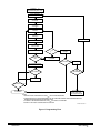
***** Print signon and warning message
bsr
Print
print signon message
dc.b
'M68F333 Flash EEPROM Programmer Version 2.0',13,10,0
*
***** Main initialisation
bsr
Initialize
tst
d0
bne
Prog_end
*
Prog_0
*
Prog_1
***** Check command line
cmpi
#2,d2
bcs
Prog_0
cmpi
#3,d2
bls
Prog_1
move
#UsageError,Error(A5)
bra
Prog_end
Prog_12
*
Prog_2
clr.w
cmpi
bne
move.l
bsr
beq
move
bra
move.l
move.w
MOTOROLA
16
#4,a2
(a2)+,a0
FileMode(A5),a1
fopen
d0,FilePtr(A5)
Prog_11
#FileError,Error(A5)
Prog_end
skip over program name
get file name of S records
read mode - "r"
save file pointer
continue if OK
can't open input file
ModeAddr(A5)
#3,d2
Prog_2
(a2)+,a0
Eval
Prog_12
#EvalError1,Error(A5)
Prog_3
d1,StartAddr(A5)
#$1,ModeAddr(A5)
Assume no offset first..
argv = 3 ?
evaluate start address parameter
close file and exit
got first param
signal to calculate offset
ReadSRecord
d0
Prog_25
#SRecS9,d0
Prog_3
#SRecError,d0
d0,Error(A5)
Prog_3
get next S Record
continue if no error
S9 record ?
yes - close normally
otherwise flag error
***** Program data from S-Record into EEPROM
ProgRecord
d0
Prog_2
not_prog
#ProgError,Error(A5)
program data from S Record
loop till done
print fault address
error - report it
***** Close input file
bsr
*
Prog_end
arg count is wrong
***** Read an S-Record, check for errors
bsr
tst
beq
bsr
move
*
Prog_3
argc > 3?
***** Evaluate remaining parameters
bsr
tst
beq
cmpi
beq
addi
move
bra
*
Prog_25
argc < 2?
***** Get filename, open file, check if OK
addq.l
move.l
lea.l
bsr
move.w
bne
move
bra
*
Prog_11
init hardware and address list
CloseInputFile
close file
***** Report any errors, exit back to BD32
move
Error(A5),d1
get error code
moveq.l #BD_QUIT,d0
exit program
bgnd
AN1255/D
*****************************************************************************
* ReadSRecord - reads one S record from FilePtr
* Exit
- d0 contains returned status
*
d1 corrupted
*
a0 points to s-record (buffer)
*****************************************************************************
ReadSRecord
move.w FilePtr(A5),d1
file pointer
lea.l
buffer(A5),a0
point to S Record buffer
moveq.l #BD_FREADSREC,d0
bgnd
rts
*****************************************************************************
* CloseInputFile - closes FilePtr
* Exit
- d0 corrupted
*
d1 corrupted
*
does not affect Error
*****************************************************************************
CloseInputFile move.l FilePtr(A5),d1
moveq.l #BD_FCLOSE,d0
bgnd
rts
*****************************************************************************
* Eval
- evaluates numeric string
* Entry
- string address in a0
* Exit
- result in D1, error flag in D0
*****************************************************************************
Eval
moveq.l #BD_EVAL,d0
bgnd
tst
d0
rts
*****************************************************************************
* fopen
- performs file open routine
* Entry
- filename pointer in A0
*
file mode pointer in A1
* Exit
- file pointer in D0
*****************************************************************************
fopen
moveq.l #BD_FOPEN,d0
bgnd
rts
*****************************************************************************
* FindStrEnd - searches an ASCII string for end of string
*
marker ('null'/ 0 char)
* Entry
- string pointed to by A0
* Exit
- returns a0 pointing to end of string marker
*****************************************************************************
FindStrEnd
move.w d0,-(a7)
push temp register
moveq
#-1,d0
max loop count 1st time thru
FSE_1
tst.b
(a0)+
byte == 0?
dbeq
d0,FSE_1
uses loop mode
bne
FSE_1
loop till test true
subq.l #1,a0
decrement address reg.
move.w (a7)+,d0
restore register
rts
*****************************************************************************
* ntoh
- prints hex value of register D0 least sig nibble to screen
* Entry
- D0 contains nibble value
*****************************************************************************
ntoh
movem.l d0/d1,-(a7)
move.b d0,d1
andi.w #$f,d1
addi.b #'0',d1
cmpi.b #10+'0',d1
bcs
nt_1
addi.b #'A'-'9'-1,d1
nt_1
moveq
#BD_PUTCHAR,d0
bgnd
movem.l (a7)+,d0/d1
rts
AN1255/D
MOTOROLA
17
*****************************************************************************
* btoh
- prints hex value of byte register D0 to screen
* Entry
- D0 contains byte value
*****************************************************************************
btoh
ror.b
#4,d0
bsr
ntoh
ror.b
#4,d0
bsr
ntoh
rts
*****************************************************************************
* wtoh
- prints hex value of word register D0 to screen
* Entry
- D0 contains word value
*****************************************************************************
wtoh
ror.w
#8,d0
bsr
btoh
ror.w
#8,d0
bsr
btoh
rts
*****************************************************************************
* ltoh
- prints hex value of long word register D0 to screen
* Entry
- D0 contains long word value
*****************************************************************************
ltoh
swap
d0
bsr
wtoh
swap
d0
bsr
wtoh
rts
*****************************************************************************
* Print
- prints constant string in code and returns to
*
program at first even location after string
* Entry
- parameters indexed from stacked return PC
* Exit
- stacked return PC modified to give correct return
*
no registers corrupted
*****************************************************************************
Print
movem.l a0/d0,-(a7)
save registers
*
WARNING : Any change to movem list will require change
*
to stack offset used below
move.l 8(a7),a0
get address of string
*
( = stacked return address)
moveq.l #BD_PUTS,d0
function call
bgnd
bsr
FindStrEnd
get end of ASCII string
move.l a0,d0
test for odd address
addq.l #1,d0
skip past end of string
btst
#0,d0
beq
Print_1
addq.l #1,d0
it's odd - return to next addr
Print_1
move.l d0,8(a7)
update stacked return address
movem.l (a7)+,d0/a0
get back registers
rts
done
*****************************************************************************
* crlf
- prints carriage return, line feed combo
* Exit
- no registers corrupted
*****************************************************************************
crlf
bsr
Print
carriage return, line feed
dc.b
13,10,0,0
rts
******************************************************************************
* getchar
- returns character typed by user
* Exit
- d0 contains character typed
*****************************************************************************
getchar
moveq.l #BD_GETCHAR,d0
bgnd
rts
MOTOROLA
18
AN1255/D
*****************************************************************************
* usedelay
- programmable software delay loop
* Entry
- delay in us (approximate) stored in d1,
*
legal values are 2 ... 65535
* Exit
- d1 corrupted
* Environment- timings assume 2 clock program memory access and 16.778MHz
*
clckout frequency
*****************************************************************************
*
jsr
usdelay
13
usdelay
subq
#2,d1
2 - adjust for overhead
asl
#1,d1
6 - multiply count by 2 for us
loop
tst
d1
2
dbf
d1,loop
6
rts
12
*****************************************************************************
* check_address - searches through valid flash address ranges
*
to find which array is being accessed, and therefore
*
which set of control registers to use.
*
*
Note - flash register ranges are tested first, as they
*
have priority over an array that is mapped to the same
*
address.
*
* Entry
- A0 contains address to be programmed
* Exit
- A1 contains start address of register bank, or 0 if
*
no valid flash module found for adress
*****************************************************************************
check_address
movem.l d0,-(a7)
push working reg for now
move.l a0,d0
restrict address to 24 bits
and.l
#$00ffffff,d0
move.l d0,a0
*
ca_regs
Is a0 within 16K register block?
cmpa.l
bcs
cmpa.l
*
bhi
move.l
bra
*
ca_2
Is a0 within 48K register block?
cmpa.l
bcs
cmpa.l
*
bhi
move.l
bra
*
ca_3
FEEBAH+FER_1,d0
#$00ffffff,d0
d0,a1
a1,a0
ca_4
#FEE_SIZE_1-1,d0
d0,a1
a1,a0
ca_4
#FER_1,a1
ca_good
read array1 start address
clear d0[31:24]
is a0 > range start?
calculate end addresses
is a0 < range end?
yes, within range
Is a0 within 48K flash array?
move.l
and.l
move.l
cmpa.l
bcs
add.l
AN1255/D
#FER_2&$ffffff,a0
range 2 start test..
ca_3
is a0 > range start?
#(FER_2+FER_REGSZ-1)&$ffffff,a0
yes, now test against end..
ca_3
is a0 < range end?
#FER_2,a1
yes, within range
ca_good
Is a0 within 16K flash array?
move.l
and.l
move.l
cmpa.l
bcs
add.l
move.l
cmpa.l
bhi
move.l
bra
*
ca_4
#FER_1&$ffffff,a0
range 1 start test..
ca_2
is a0 > range start?
#(FER_1+FER_REGSZ-1)&$ffffff,a0
yes, now test against end..
ca_2
is a0 < range end?
#FER_1,a1
yes, within range
ca_good
FEEBAH+FER_2,d0
#$00ffffff,d0
d0,a1
a1,a0
ca_bad
#FEE_SIZE_2-1,d0
read array2 start address
clear d0[31:24]
is a0 > range start?
calculate end addresses
MOTOROLA
19
move.l
cmpa.l
bhi
move.l
bra
*
ca_bad
d0,a1
a1,a0
ca_bad
#FER_2,a1
ca_good
is a0 < range end?
yes, within range
No valid module being addressed - return 0 in A1
movea.l #0,a1
ca_good
movem.l (a7)+,d0
rts
*******************************************************************************
* do_prog
- Programs one byte/word of data to memory
* Entry
- Target address in A0
*
byte or word data in D0
*
byte flag in d5 (non-zero => program byte data)
* Exit
- d0 contains difference between data to be programmed and read
*
back data ($00 if programming successful)
*
or $ff if address to be programmed is not recognised as flash
*
d3 is corrupted
*
a0 and d5 are unchanged
*******************************************************************************
do_prog
bsr
dis_both
disable both modules (STOP)
clr.w
d3
initialise pulse counter = 0
bsr
check_address
get register address
tst.l
beq
a1
dp_addrfail
address OK?
no - bomb out
move.w
move
tst
beq
#flashen,FEEMCR(a1)
#latch,FEECTL(a1)
d5
dp_word
only enable module to be programmed
enable verify + latch
byte or word?
*
** Byte data to programming latch
move.b d0,(a0)
write byte data to EEPROM
bra
dp_prgloop
*
dp_word
** Word data to programming latch
move.w d0,(a0)
write word data to EEPROM
*
dp_prgloop
** Initialise prog pulse time
move.w #pwpp,d1
pulse time ready for usdelay
*
** Programming stage
move.w #prgen,FEECTL(a1)
bsr.w
usdelay
enable prog voltage : set ENPE
wait pwpp microseconds
*
*
dp_verw
dp_vertst
*
** 'Off' time
move.w #latch,FEECTL(a1)
disable voltage : clear ENPE
move.w #tpr,d1
delay tpr microseconds after turning off vprog
bsr
usdelay
addq.w #1,d3
increment pulse count
** Verify stage - store diff in d0
moveq.l #0,d0
d0 ready to hold byte/word diff.
tst
d5
byte or word?
beq
dp_verw
move.b (a0),d0
byte verify
bra
dp_vertst
move.w (a0),d0
word verify
beq
dp_margin
verify O.K?
** Failed to verify
cmpi.w #npp,d3
bcs
dp_prgloop
over max number of program pulses?
no - continue
*
** Failed to verify and max program time used
move.w #norm,FEECTL(a1)
normal flash reads/writes
bra
dp_end
return programming data error to caller
*
** programmed OK - now re-program for the same number of pulses (100% margin)
MOTOROLA
20
AN1255/D
dp_margin
dp_mrgloop
subq.w
move.w
move.w
bsr
move.w
move.w
bsr
dbf
*
*
** Check still programmed - store diff in d0
moveq.l #0,d0
d0 ready to hold byte/word diff.
tst
d5
byte or word?
beq
dp_verw2
move.b (a0),d0
byte verify
bra
dp_vertst2
move.w (a0),d0
word verify
move.w #norm,FEECTL(a1)
normal flash reads/writes
bra
dp_end
return programmed data to caller
(don't need to test)
*
dp_addrfail
** check_address address fail
move.w #$ff,d0
force fail because of bad address
*
dp_end
** Fail + pass termination
bsr
dis_both
rts
disable both modules
and quit
dp_verw2
dp_vertst2
#1,d3
#pwpp,d1
#prgen,FEECTL(a1)
usdelay
#latch,FEECTL(a1)
#tpr,d1
usdelay
d3,dp_mrgloop
compensate for extra dbcc loop
set program pulse time
enable prog voltage : set ENPE
and delay
disable voltage : clear ENPE
set program recovery time
and delay
count down pulses
*****************************************************************************
* Initialize - initialize routine is called by BD32 before any programming
*
initialize and check main registers
*
initialize global variables
*
returns non-zero in D0 if can't continue with programming
*
* Exit
- d0 cleared
*****************************************************************************
Initialize
*
(Initialise modules but leave STOPped)
*
***** Initialisation module 1 main registers
move.w
move.w
#flashdis,FEEMCR+FER_1
#$4,FEECTL+FER_1
STOP module 1
make sure verify mode off
*
***** Initialisation module 2 main registers
move.w #flashdis,FEEMCR+FER_2 STOP module 2
move.w #$4,FEECTL+FER_2
make sure verify mode off
*
***** Now initialize globals
clr.l
d0
move
#ProgdOK,Error(A5)
rts
no error function return value
initialise successful return value
done - return no error
*****************************************************************************
* ProgRecord - programs data from S-record buffer into EEPROM
*
loops through the record, retrieving each byte/word and
*
programming it at the specified S-record address + OffsetAddr
*
*
IF ModeAddr == $1, OffsetAddr is calculated so that :
*
(OffsetAddr + S-record address) = StartAddress
*
(where StartAddress is user specified) and ModeAddr is then
*
cleared
*
* Entry
- no parameters: assumes S Record is in 'buffer'
* Exit
- d0 is difference between data and EEPROM location
*
(this will be 0 if programmed successfully)
*
a0 will contain address at which program failed
*
d5 will be non-zero if byte program, 0 if word program
*****************************************************************************
ProgRecord
movem.l a1/a2/d6,-(a7)
save working registers
lea.l
buffer(A5),a2
point to S-record buffer
clr.l
d6
move.b (a2)+,d6
get record type
beq
AN1255/D
prog_good
record type 0 (header)
MOTOROLA
21
*
- exit as no data to program
cmpi.b
bcs
#7,d6
prog_start
bra
prog_good
record type >3, (not code/data)
- exit as no data to program
move.b
subi.b
move.l
(a2)+,d6
#4,d6
(a2)+,a0
get byte count from s-record
remove byte count due to address
get address (note : BD32 always
stores 4 byte address field)
#$1,ModeAddr(A5)
prog_addoff
a0,d5
StartAddr(a5),a1
d5,a1
a1,OffsetAddr(a5)
ModeAddr(A5)
OffsetAddr(a5),a0
Should we calculate offset?
prog_addoff
cmpi.w
bne
move.l
move.l
suba.l
move.l
clr.w
adda.l
prog_1
move.l
a0,d5
store address in d5
andi.l
bne
cmpi
bne
#1,d5
prog_2
#1,d6
prog_3
mask all but bit 0
program byte if odd address
count == 1?
word program if not
*
*
prog_start
*
prog_offs
record type 1,2 or 3 (code/data)
- start programming
put address in d5
Yes, get desired start
..use to calculate offset
..store
..clear mode to signal done
add offset to address
* program byte data if address is odd or byte count is 1
prog_2
moveq
move.b
bsr
tst.w
beq
#1,d5
(a2),d0
do_prog
d0
prog_25
flag byte write
byte - get data
program byte/word
programmed O.K?
quit1
bsr
bne
not_progd
prog_done
no - does user want to quit?
*
*
prog_25
Either programmed O.K. (byte), or user wishes to continue
addq.l
addq.l
subq
bne
bra
#1,a0
#1,a2
#1,d6
prog_1
prog_good
increment target address
increment buffer address
dec byte count
loop till byte count = 0
otherwise done
* program word data if address is even and byte count not equal to 1
prog_3
move.b
asl.w
move.b
(a2)+,d0
#8,d0
(a2)+,d0
get word - we don't know if
..data in buffer is word aligned
..so read two bytes
bsr
tst.w
beq
do_prog
d0
prog_35
program byte/word
programmed O.K?
quit2
bsr
bne
not_progd
prog_done
no - does user want to quit?
*
*
prog_35
Either programmed O.K. (word), or user wishes to continue
prog_good
prog_done
moveq.l #0,d0
movem.l (a7)+,a1/a2/d6
rts
MOTOROLA
22
addq.l
subq
bne
#2,a0
#2,d6
prog_1
increment target address
dec byte count
loop till byte count = 0
no error
restore registers
done
AN1255/D
******************************************************************************
* not_progd
- informs user of programming error
* not_blank
- informs user of blank check error
*
user enters escape to stop, any other key to continue programming
* exit
- d0 is $0 and Z flag is set if user wants to continue
*
d0 is non-zero, and Z flag is clear if user wants to abort
*****************************************************************************
not_progd:
bsr
Print
dc.b
'prog: program fail at address $',0
bra
n_b1
not_blank:
n_b1
bsr
dc.b
move.l
bsr
Print
'prog: EEPROM not blank, address $',0
a0,d0
print address
ltoh
bsr
dc.b
bsr
move
bsr
move
andi
cmpi
seq
tst
rts
Print
13,10,'prog: Press <esc> to stop, any other to continue: ',7,0
getchar
d0,-(a7)
save char
crlf
(a7)+,d0
get char
#$ff,d0
#$1b,d0
escape?
d0
make d0 nonzero if so
d0
set SR for subsequent test
******************************************************************************
* not_prog
- informs user of programming error
* Entry
- a0 contains fault address
*****************************************************************************
not_prog:
bsr
Print
dc.b
'prog: program failed before $',0
move.l a0,d0
print address
bsr
ltoh
bsr
crlf
rts
******************************************************************************
* dis_both
- disables both flash EEPROM modules
* exit
- no registers modified
*****************************************************************************
dis_both
move.w
move.w
rts
end
#flashdis,FEEMCR+FER_1
#flashdis,FEEMCR+FER_2
disable module 1 (set STOP)
disable module 2 (set STOP)
******************************************************************************
* Prog msg
- message file for programming driver
*****************************************************************************
prog
prog:
prog:
prog:
prog:
prog:
prog:
prog:
prog:
prog:
prog:
prog:
<filename> [<start>]
program M68F333 flash EEPROM from file
Usage error: prog <filename> [<start address>]
Error opening input file
Error evaluating <start> address parameter
End of file reached before S7/S8/S9 record was read
S9 record read - file closed normally
Checksum error in S-Record input file
Format error in S-Record input file; file is probably not S-Records
Programming error - check Vfpe / EEPROM is blank
Unhandled exception encountered
Programming completed O.K.
AN1255/D
MOTOROLA
23
BULK — Erasure Driver
User Details
The BULK driver performs bulk erasure of a single flash EPROM module. The syntax used is:
BULK
<module id>
The argument <module id> is used to specify the module to be erased. The value can be either ‘16’ or ‘48’
to specify the 16 kbyte or 48 kbyte Flash EEPROM modules respectively. A series of erasure passes are
used. Each successive pulse is of progressively longer duration, until erasure is verified. Each erasure pass
is indicated by the printing of a period, and if erasure is not verified after the maximum erasure time has
been used, a bulk fail message is printed, along with the address of the first failed location.
As with the PROG driver, the BULK driver does not map the flash array to a particular address. The user
must make certain that the array address does not conflict with addresses of other MCU modules, causing
erasure to fail. The array can be relocated either by programming the shadow registers and then resetting
the device, or by directly reconfiguring the base address registers. The base address registers can only be
changed when the FLASH module LOCK bit is cleared.
Software Details
The BULK software applies erase pulses of increasing duration until the array and shadow registers verify
as erased, then a final erase pulse is applied as an erase margin.
The source files for the BULK driver software are:
BULK.S62
Erase code source file
BULK.MSG
Message text file used by BD32
IPD.INC
Definitions required for the BD32 system calls
M68F333.INC MC68F333 constants definition file, including register addresses, other flash module
information, and programming/erasure timing data. Timing information is compatible with the definitions
used in the MC68F333 device specification to simplify updates.
Common include files used by both drivers are shown after the erasure driver code.
MOTOROLA
24
AN1255/D
BULK Driver Listing
*****************************************************************************
* 'BULK' Resident Command Driver for MC68F333 device
*
* Utility to bulk erase an MC68F333 flash EPROM module
*
* Source file
: bulk.s62
* Object file
: bulk.d32
* Include files : M68F333.inc
(M68F333 addresses and programming constants)
*
ipd.inc
(BD32 system call constants)
* Message file : bulk.msg
*
* Object file format: Motorola S-records
*
* Execute from BD32 as: bulk <module ID>
*
Module ID can be '16' or '48' and specifies which MC68F333 flash
*
module is to be bulk erased.
*
* Addressing modes : This code is designed as a driver for the BD32 background
*
debugger for CPU32 devices. A requirement is that the code must be
*
fully relocateable. All addresses (apart from fixed module addresses)
*
are relative, and where word alignment is not guaranteed, byte
*
accesses must be used.
*
Supervisor program space accesses are used when reading the flash
*
array to allow operation regardless of the configuration of the
*
flash modules's ASPC bits (FEEMCR).
*
* Word alignment : The embedded text strings have been adjusted in size so
*
that the following code remains word aligned - any modifications
*
to these strings should be adjusted accordingly. An assembler
*
'even' type directive to force word-alignment could be used if
*
available.
*****************************************************************************
*
Include files
lib
ipd.inc
BD32 call code definitions
lib
M68F333.inc
M68F333 device constants
*
BD32 return error codes : see file BULK.MSG for associated text
UsageError
BulkError
ExcepError
PassError
equ
equ
equ
equ
*
SRecS9
BD32 call return codes : see bd32 file BD32.DOC
equ
2
S9 Record - end of file
*
ErasedValue
sup_prog
General constants
equ
$ffff
equ
$6
*
*
flashdis
*
flashen
*
*
erase_on
erase_off
norm
*
1
2
3
4
Usage: ...
error programming data
unhandled exception
erase successful
erased state of EEPROM
supervisor/program space code
Flash control register constants
FEEMCR
equ
$90c0
Module DISABLED, disable VFPE in BDM,
no boot, unrestricted space, 2 cycle access
equ
$10c0
Module ENABLED, disable VFPE in BDM,
no boot, unrestricted space, 2 cycle access
FEECTL
equ
$7
Erase, VFPE enabled
(VFPE,ERAS,LAT,ENPE set)
equ
$6
Erase, VFPE disabled
(VFPE,ERAS,LAT set)
equ
$0
No programming/erase
(All cleared)
Variable area
section .data
dc.l
Bulk
ds.l
30
*
stack
start address (add load offset)
Stack area
initial stack pointer
ModSize
ModAddress
StartAddress
dc.l
dc.l
dc.l
$0
$0
$0
Module size
Module address
Start array address
Error
ds.w
1
error code
AN1255/D
MOTOROLA
25
Era_shadow
dc.w
dc.w
dc.w
dc.w
$9B00,$0000,$FFFF,$E000 erased shadow register mask
$0000,$0000,$0000,$0000 used for verification of erase
$FFFF,$FFFF,$FFFF,$FFFF
$0000,$0000,$0000,$0000
*****************************************************************************
*
CUSTOM VECTOR TABLE
*****************************************************************************
vectable
ds.l
13
Alternate vector table
*****************************************************************************
*
EXCEPTION HANDLER ROUTINE
*
Use - Quits to BD32 with unhandled exception error code
*
Exception handling is included because many user errors
*
(mapping of flash/drivers etc) could cause bus errors,
*
f-line exceptions etc. Flash programming voltage is disabled
*
in case exception ocurred during a programming cycle
*****************************************************************************
excep_h
move.w #norm,FEECTL(a1)
normal flash reads/writes
*
disable programming voltage
move
#ExcepError,Error(A5)
unhandled excep error
bra
Bulk_end
FileMode
dc.b
'r',0
read mode for file open
*****************************************************************************
*
Execution start of driver 'BULK'
*
Entry (from BD32) :
*
d0 - number of driver parameters
*
a0 - address of parameter array
*
a5 - driver offset address
*****************************************************************************
Bulk
*
***** Exception handler initialisation
lea.l
vectable(PC),a1
get start of vector table
movea.l a1,a2
working (loop) copy
lea.l
excep_h(PC),a3
get address of handler
move.w #$0c,d1
initialise copy loop
vecloop
move.l a3,(a2)+
build new vector table
dbf
d1,vecloop
movec.l a1,vbr
set up vbr for new table
*
***** SP and general register initialisation
lea.l
stack(A5),a7
set up stack
lea.l
stack(PC),a7
set up stack
move.l a0,a2
get argv into a2
move.l d0,d2
get argc into d2
*
***** Print signon and warning message
bsr
dc.b
*
*
Bulk_1
MOTOROLA
26
Print
print signon message
'M68F333 Flash EEPROM Bulk Eraser Version 2.0 ',13,10,0
***** Check command line
cmpi
#2,d2
beq
Bulk_1
move
#UsageError,Error(A5)
bra
Bulk_end
argc = 2?
arg count is wrong
***** Get module parameter, and use to set up ModAddress
move.l
move.l
addq.l
move.l
#FER_1,ModAddress(a5)
assume 16K module initially
#FEE_SIZE_1,ModSize(a5)
#4,a2
skip over program name
(a2)+,a0
get address of parameter
move.b
asl.w
move.b
(a0)+,d0
#8,d0
(a0)+,d0
get two bytes of parameter
(data in buffer may not be
word aligned so read 2 bytes)
AN1255/D
cmpi.w
beq
move.l
move.l
cmpi.w
beq
move
bra
#'16',d0
Bulk11
#FER_2,ModAddress(a5)
#FEE_SIZE_2,ModSize(a5)
#'48',d0
Bulk11
#UsageError,Error(A5)
Bulk_end
16k array specified?
yes, so O.K. to continue..
no, so first assume 48k
..and then verify
yes, so O.K. to continue..
no, so flag useage error
..and quit
*
Bulk11
***** Initialise module, and calculate array addresses
bsr
Initialize
init hardware
*
***** Erase module now
bsr
Erase
tst.b
d0
beq
Bulk_end
was erase succesful?
move
bra
no, so flag erase error
*
Bulk_end
#BulkError,Error(A5)
Bulk_end
***** Report any errors, exit back to BD32
move
Error(A5),d1
get error code
moveq.l #BD_QUIT,d0
exit program
bgnd
*****************************************************************************
* FindStrEnd - searches an ASCII string for end of string
*
marker ('null'/ 0 char)
* Entry
- string pointed to by A0
* Exit
- returns a0 pointing to end of string marker
*
all other registers preserved
*****************************************************************************
FindStrEnd
move.w d0,-(a7)
push temp register
moveq
#-1,d0
max loop count 1st time thru
FSE_1
tst.b
(a0)+
byte == 0?
dbeq
d0,FSE_1
uses loop mode
bne
FSE_1
loop till test true
subq.l #1,a0
decrement address reg.
move.w (a7)+,d0
restore register
rts
*****************************************************************************
* ntoh
- prints hex value of register D0 least sig nibble to screen
* Entry
- D0 contains nibble value
* Exit
- all registers preserved
*****************************************************************************
ntoh
movem.l d0/d1,-(a7)
move.b d0,d1
andi.w #$f,d1
addi.b #'0',d1
cmpi.b #10+'0',d1
bcs
nt_1
addi.b #'A'-'9'-1,d1
nt_1
moveq
#BD_PUTCHAR,d0
bgnd
movem.l (a7)+,d0/d1
rts
*****************************************************************************
* btoh
- prints hex value of byte register D0 to screen
* Entry
- D0 contains byte value
* Exit
- all registers preserved
*****************************************************************************
btoh
ror.b
#4,d0
bsr
ntoh
ror.b
#4,d0
bsr
ntoh
rts
AN1255/D
MOTOROLA
27
*****************************************************************************
* wtoh
- prints hex value of word register D0 to screen
* Entry
- D0 contains word value
* Exit
- all registers preserved
*****************************************************************************
wtoh
ror.w
#8,d0
bsr
btoh
ror.w
#8,d0
bsr
btoh
rts
*****************************************************************************
* ltoh
- prints hex value of long word register D0 to screen
* Entry
- D0 contains long word value
* Exit
- all registers preserved
*****************************************************************************
ltoh
swap
d0
bsr
wtoh
swap
d0
bsr
wtoh
rts
*****************************************************************************
* Print
- prints constant string in code and returns to
*
program at first even location after string
* Entry
- parameters indexed from stacked return PC
* Exit
- stacked return PC modified to give correct return
*
all registers preserved
*****************************************************************************
Print
movem.l a0/d0,-(a7)
save registers
move.l 8(a7),a0
get address of string
*
( = stacked return address)
moveq.l #BD_PUTS,d0
function call
bgnd
bsr
FindStrEnd
get end of ASCII string
move.l a0,d0
test for odd address
addq.l #1,d0
skip past end of string
btst
#0,d0
beq
Print_1
addq.l #1,d0
it's odd - return to next addr
Print_1
move.l d0,8(a7)
update stacked return address
movem.l (a7)+,d0/a0
get back registers
rts
done
*****************************************************************************
* crlf
- prints carriage return, line feed combo
* Entry
- no parameters
* Exit
- all registers preserved
*****************************************************************************
crlf
bsr
Print
carriage return, line feed
dc.b
13,10,0,0
*
even
rts
******************************************************************************
* getchar
- returns character typed by user
* Entry
- no parameters
* Exit
- d0 contains character typed
*****************************************************************************
getchar
moveq.l #BD_GETCHAR,d0
bgnd
rts
*****************************************************************************
* msdelay
- programmable milliseconds delay
* Entry
- delay time in ms in d1
*
legal values are 1 ... 65535
* Exit
- d1 corrupted
*
Note - routine calibrated for 16.78MHz clock / 2 clock memory
*****************************************************************************
msdelay
move.l d2,-(a7)
preserve d2
subq.w #1,d1
compensate for dbcc offset of 1
move.w #$826,d2
initialise inner loop count to
*
compensate for entry overhead
MOTOROLA
28
AN1255/D
loop
loop2
tst
tst
dbf
move.w
dbf
move.l
rts
d1
d2
d2,loop2
#$82d,d2
d1,loop
(a7)+,d2
inner loop count
restore d2
*****************************************************************************
* Erase
- bulk erase routine
*
performs erase algorithm until maximum allowed erase pulses
*
used, or array has verified as correctly erased
* Entry
- module defined by ModAddress
*
ModSize
* Exit
- D0 is non zero if erase unsuccessful
*
A0 contains first error address if erase unsuccessful,
*
otherwise A0 corrupted
*
All other registers unchanged
*****************************************************************************
Erase
movem.l d1-d3/a1,-(a7)
preserve registers
*
*
***** Initialise timing and address parameters
clr.w
d2
initialise pulse counter k = 0
clr.w
d3
initialise cumulative erase time = 0
(used as erase margin)
move.l ModAddress(a5),a1
get module address into a1
move.w
move.w
*
db_1
*
*
*
*
#erase_off,FEECTL(a1)
d0,(a1)
set VFPE/ERAS/LAT
write data to EEPROM
***** Erase cycle
bsr
Print
dc.b
'.',$0
addq.w #1,d2
print 'progress dots'
***** Calculate erase time
move.w #tei,d1
mulu.w d2,d1
add.w
d1,d3
erase pulse time = tei
* k (ms) = d1
add to cumulative time, d3
***** Apply erase pulse
move.w #erase_on,FEECTL(a1)
bsr
msdelay
move.w #erase_off,FEECTL(a1)
enable prog voltage : set ENPE
wait tei*k milliseconds
disable voltage : clear ENPE
***** Recovery 'Off' time
move.w #ter,d1
bsr
msdelay
delay erase recovery time, ter
***** Blank test array
bsr
check_array
tst.b
d0
bne
db_q
array now blank?
increment pulse counter, k
miss register test if array non-blank
*
***** Blank test shadow registers
bsr
check_regs
registers now blank?
tst.b
d0
beq
db_2
*
db_q
***** Array and/or registers not blank
cmpi.w #nep,d2
used max pulses, k>=nep?
bcs
db_1
no - continue
*
***** Fail, so print error message and quit
move.w #norm,FEECTL(a1)
yes - flag and quit
bsr
Print
dc.b
13,10,'bulk: erase failed address $',0
move.l a0,d0
print address
bsr
ltoh
bsr
crlf
move.w #$1,d0
flag error in d0
bra
db_end
AN1255/D
MOTOROLA
29
*
db_2
*
db_end
***** Erase verifies OK - now add erase margin
move.w d3,d1
erase margin time (em)
= sum of erase pulses = d3
move.w #erase_on,FEECTL(a1)
enable prog voltage : set ENPE
bsr
msdelay
delay em
move.w #erase_off,FEECTL(a1)
disable voltage : clear ENPE
move.w
bsr
#ter,d1
msdelay
delay erase recovery time, ter
move.w
clr.l
#norm,FEECTL(a1)
d0
normal accesses
clear d0 to signal success
movem.l (a7)+,d1-d3/a1
rts
restore registers
*****************************************************************************
* Initialize - initialize routine is called by BD32 before bulk erasing
*
initialize main flash registers
*
initialize global variables
*
returns non-zero in D0 if can't continue with programming
*
* Entry
- flash module address (register block) in ModAddress(a5)
*
* Exit
- d0 cleared
*
all other CPU registers preserved
*
flash array address written to StartAddress(a5)
*****************************************************************************
Initialize
movem.l a3-a4,-(a7)
preserve registers
*
(Initialise modules but leave STOPped)
*
***** Initialisation and STOP module 1
move.w #flashdis,FEEMCR+FER_1 STOP module 1
move.w #norm,FEECTL+FER_1
make sure verify mode off
*
***** Initialisation and STOP module 2
move.w #flashdis,FEEMCR+FER_2 STOP module 1
move.w #norm,FEECTL+FER_2
make sure verify mode off
*
***** Start-up module to be erased, and get array addresses
move.l ModAddress(a5),a3
get module address into a3
move.w #flashen,FEEMCR(a3)
clear STOP
movea.l FEEBAH(a3),a4
get array start address
move.l a4,StartAddress(a5)
and store
move
#PassError,Error(A5)
movem.l (a7)+,a3-a4
rts
initialise to successfull erase code
restore registers
done - return no error
*****************************************************************************
* check_array - checks EEPROM array contents all are ErasedValue
*
* Entry
- StartAddress, ModSize parameters initialised
*
* Exit
- if array checks as ErasedValue
*
d0 = 0
*
a0 corrupted
*
D1 corrupted
*
else
*
d0 = 1
*
a0 = error address
*
d1 = error data
*****************************************************************************
check_array
movem.l d2,-(a7)
preserve registers
move.l #sup_prog,d0
configure array accesses as
movec
d0,sfc
..supervisor/program space
move.l StartAddress(a5),a0
array start in a0
move.l ModSize(a5),d1
array size in d1
MOTOROLA
30
AN1255/D
asr.l
subq.l
move.w
bc_1
#1,d1
#1,d1
#ErasedValue,d0
moves.w (a0)+,d2
cmp.w
d2,d0
dbne
d1,bc_1
calculate array size in words
set up for dbcc loop
get erased value of EEPROM
get array word from supervisor/program space
test (== ErasedValue?)
loop while equal, and not end of array
beq
bc_2
loop exit because of error?
move.w
move.b
bra
d2,d1
#$01,d0
bc_3
yes, put error data in d1,
and flag error, array not blank
bc_2
clr.l
d0
no, flag no error, array tests OK
bc_3
movem.l (a7)+,d2
rts
restore registers
*****************************************************************************
* check_regs - routine to blank check flash shadow registers for a module
*
with register start address specified in a0
*
* Entry
- a0 should contain register start address
* Exit
- if verified blank d0 = 0
*
else d0 = 1
*
d1= fault data
*
and a0 = fault address
*****************************************************************************
check_regs
movem.l d2-d3/a1-a2,-(a7)
preserve registers
move.l ModAddress(a5),a0
get module address into a0
move.l a0,a2
use a2 as general pointer
*
***** Check shadow registers against erased values table
move.w #15,d1
number of word checks (loop cnt.)
lea.l
(Era_shadow,a5),a1
table address in a1
cr_loop
move.w
move.w
and.w
cmp.w
bne
dbf
clr.l
bra
*
cr_bad
(a2)+,d2
d2,d3
(a1),d2
(a1)+,d2
cr_bad
d1,cr_loop
d0
cr_end
get a shadow register value,
store,
ignore un-implemented bits,
and check erased..
O.K?
yes, loop if not finished
finished - signal blank check OK
and return
***** Un-erased shadow register found - notify and abort
suba.l
move.w
move.w
#2,a2
d3,d1
#1,d0
get correct fault address
and fault data
flag fault
cr_end
move.l a2,a0
movem.l (a7)+,d2-d3/a1-a2
rts
end
return fault address (if any)
restore registers
*****************************************************************************
* Bulk msg
- message file for bulk erase driver
*****************************************************************************
BULK
bulk:
bulk:
bulk:
bulk:
<16/48>
Bulk erase Orion 16k/48k EEPROM modules
usage error: BULK <16/48>
bulk erase failed
unhandled exception encountered
module erased O.K.
AN1255/D
MOTOROLA
31
Initialization Files Used By Program and Erase Drivers
*****************************************************************************
* 'M68F333.INC' Define M68F333 addresses and programming constants
*****************************************************************************
FER_1
FEE_SIZE_1
FER_2
FEE_SIZE_2
FER_REGSZ
equ
equ
equ
equ
equ
$FFFFF800
$4000
$FFFFF820
$c000
$20
register block address for array #1 - 16k bytes
size of array #1 - 16k bytes
registers block address for array #2 - 48k bytes
size of array #2 - 48k bytes
size of register block (both arrays)
0
2
4
6
8
$10
$12
$14
$16
mod config register
test register
base address reg - high word
base address reg - low word
program control reg
bootstrap info 0
bootstrap info 1
bootstrap info 2
bootstrap info 3
* register offsets
FEEMCR
FEETST
FEEBAH
FEEBAL
FEECTL
FEEBS0
FEEBS1
FEEBS2
FEEBS3
equ
equ
equ
equ
equ
equ
equ
equ
equ
* bit assignments
STOP
FRZ
BOOT
LOCK
ASPC1
ASPC0
WAIT1
WAIT0
equ
equ
equ
equ
equ
equ
equ
equ
$8000
$4000
$1000
$800
$200
$100
$80
$40
FSTE
GADR
HVT
BTST
STRE
MWPF
equ
equ
equ
equ
equ
equ
$80
$40
$20
$10
2
1
VFPE
ERAS
LAT
ENPE
equ
equ
equ
equ
8
4
2
1
* Flash EEPROM timing constants
* Programming constants
pwpp
equ
&20
tpr
equ
&10
npp
equ
&50
program pulse width (us)
program recovery time (us)
number of program pulses
* Erase constants
tei
equ
ter
equ
nep
equ
erase pulse increment time (ms)
erase recovery time (ms)
maximum number of erase pulses
100
1
5
* end of M68F333.inc
MOTOROLA
32
AN1255/D
*****************************************************************************
* ipd.inc - equates for BD32 systems calls
*****************************************************************************
BD_QUIT
BD_PUTS
BD_PUTCHAR
BD_GETS
BD_GETCHAR
BD_GETSTAT
BD_FOPEN
BD_FCLOSE
BD_FREAD
BD_FWRITE
BD_FTELL
BD_FSEEK
BD_FGETS
BD_FPUTS
BD_EVAL
BD_FREADSREC
equ
equ
equ
equ
equ
equ
equ
equ
equ
equ
equ
equ
equ
equ
equ
0
1
2
3
4
5
6
7
8
9
10
11
12
13
14
equ
quit - return to BD32
puts - put string to console
putchar - print character on console
gets - get string from user
getchar - get single character from user
getstat - return 1 if character waiting from user
fopen - open disk file with specified mode
fclose - close disk file
fread - read from disk file
fwrite - write to disk file
ftell - report current pointer position
fseek - seek disk file to given position
fgets - read string from file
fputs - write string to file
eval - evaluate arithmetic expression
15 read s-record
* end of ipd.inc
PROGRAMMING/ERASURE EXAMPLES
The following examples show various program and erase operations. In all of the examples, keyboard input
from the user is shown as bold text.
Example 1 - Programming The FLASH Modules
This example shows operations required to program the both 16 kbyte and 48 kbyte flash modules from
their erased state. Programming data for the shadow registers is in the file TEST1R.0, while programming
data for the arrays is in the file ARRAY64.0.
First, initialize MCU memory resources to allow the driver software to execute. In this case, the file SRAMHIGH.DO is used to configure the on-chip TPURAM and SRAM.
BD32->do sramhigh.do
The file SRAMHIGH.DO initializes the device, and terminates by checking that the required memory resources are responding correctly. This is done by writing the first few bytes of TPURAM and SRAM, and
then reading them back. The flash register blocks are also displayed.
The macro file prints the following results.
BD32->* Finished, should have
BD32->*
BD32->*
BD32->*
BD32->*
BD32->*
BD32->* Test read of TPURAM:
BD32->md $100000 $10
00100000 5450 5520 5241 4D20
BD32->*
BD32->* Test read of SRAM:
BD32->md $100e00 $10
00100E00 5352 414D 206D 656D
BD32->*
BD32->* Flash register area:
BD32->md $fff800 $40
AN1255/D
TPURAM $100000 - $100e00,
SRAM
$100e00 - $100fff
SSP
$100ffe
Drivers load @
$100000
6D65 6D6F 7279 2020
TPU RAM memory
6F72 7920 2020 2020
SRAM memory
MOTOROLA
33
00FFF800
00FFF810
00FFF820
00FFF830
9BC0
FFFF
9BC0
FFFF
0000
FFFF
0000
FFFF
00FF
FFFF
00FF
FFFF
C000
FFFF
0000
FFFF
0000
0000
0000
0000
0000
0000
0000
0000
0000
0000
0000
0000
0000
0000
0000
0000
.@....@.........
................
.@..............
................
NOTE
Ensure that the VFPE supply is enabled before the programming command is entered.
The base address registers are programmed to ensure that the array is correctly mapped:
BD32->prog test1r.0
($100036).....................................................
Download completed OK - 53 records read
M68F333 Flash EEPROM Programmer Version 2.0
prog: Programming completed O.K.
At this point, the shadow registers are programmed with appropriate values, but the MCU must be reset for
these to take effect. The initialization file SRAMHIGH.DO resets the MCU as one of its operations. If either
of the flash modules have been programmed with the boot option enabled, it is best to disable them by holding DATA[15:14] low during rest.
BD32->do sramhigh.do
The macro file terminates with the following information:
BD32->* Finished, should have
BD32->*
BD32->*
BD32->*
BD32->*
BD32->*
BD32->* Test read of TPURAM:
BD32->md $100000 $10
00100000 5450 5520 5241 4D20
BD32->*
BD32->* Test read of SRAM:
BD32->md $100e00 $10
00100E00 5352 414D 206D 656D
BD32->*
BD32->* Flash register area:
BD32->md $fff800 $40
TPURAM $100000 - $100e00,
SRAM
$100e00 - $100fff
SSP
$100ffe
Drivers load @
$100000
00FFF800
00FFF810
00FFF820
00FFF830
8200
0010
8200
0010
0000
FFFE
0000
FFFE
0000
0000
0001
0001
0000
1000
0000
1000
6D65 6D6F 7279 2020
TPU RAM memory
6F72 7920 2020 2020
SRAM memory
0000
0000
0000
0000
................
...~............
................
...~............
0000
0000
0000
0000
0000
0000
0000
0000
0000
0000
0000
0000
The dump of the flash control register blocks shows that the arrays are now mapped to $00000 (16 kbyte)
and $10000 (48 kbyte). These addresses are correct for the array data file ARRAY64.0, which contains a
full 64 kbytes of test data covering both arrays. Remember, the VFPE supply must remain enabled for programming to take place. ARRAY64.0 takes around 35 seconds to program.
BD32->prog array64.0
($100038).....................................................
Download completed OK - 53 records read
M68F333 Flash EEPROM Programmer Version 2.0
prog: Programming completed O.K.
Programming is successful. Disable the VFPE supply if no more operations are required.
MOTOROLA
34
AN1255/D
Example 2: Erasing The FLASH Modules
As with the programming example, the MCU is initialized to allow execution of the driver software, in this
case by using the macro file SRAMHIGH.DO.
BD32->do sramhigh.do
The macro file terminates with the following information.
BD32->* Finished, should have
BD32->*
BD32->*
BD32->*
BD32->*
BD32->*
BD32->* Test read of TPURAM:
BD32->md $100000 $10
00100000 5450 5520 5241 4D20
BD32->*
BD32->* Test read of SRAM:
BD32->md $100e00 $10
00100E00 5352 414D 206D 656D
BD32->*
BD32->* Flash register area:
BD32->md $fff800 $40
TPURAM $100000 - $100e00,
SRAM
$100e00 - $100fff
SSP
$100ffe
Drivers load @
$100000
00FFF800
00FFF810
00FFF820
00FFF830
8200
0010
8200
0010
0000
FFFE
0000
FFFE
0000
0000
0001
0001
0000
1000
0000
1000
6D65 6D6F 7279 2020
TPU RAM memory
6F72 7920 2020 2020
SRAM memory
0000
0000
0000
0000
................
...~............
................
...~............
0000
0000
0000
0000
0000
0000
0000
0000
0000
0000
0000
0000
NOTE
Ensure that the MCU VFPE supply is enabled before the erase command is entered.
The erase driver is then executed.
BD32->bulk 16
($100030)...................................
Download completed OK - 35 records read
M68F333 Flash EEPROM Bulk Eraser Version 2.0
.bulk: module erased O.K.
The message indicates that the erase is successful. The number of periods on the last message line indicates the number of erase passes used. In this instance, there is only one.
An erase failure results in the following message, which indicates the first address to fail erase verification.
As before, the number of periods on the last message line indicates the number of erase passes used. In
this case, five passes (the maximum number) are made before a failure is reported.
BD32->bulk 16
($100030)...................................
Download completed OK - 35 records read
M68F333 Flash EEPROM Bulk Eraser Version 2.0
.....bulk: erase failed address $00000002
bulk: bulk erase failed
To erase the 48 kbyte array, the following command is used.
BD32->bulk 48
($100030)...................................
Download completed OK - 35 records read
M68F333 Flash EEPROM Bulk Eraser Version 2.0
.bulk: module erased O.K.
The erase is successful, with one erase pulse required. Disable VFPE if no more operations are required.
AN1255/D
MOTOROLA
35
Example 3 - Attempting To Erase A Conflicting Array
When the 16 kbyte array is mapped to its default erased address of $FFFFC000, portions of the array coincide with other MCU register blocks, such as the ADC control registers, which start at $FFFF700. Since
control registers generally take precedence in the memory map, erasure will fail as the erase driver attempts
to verify that the array is blank.
BD32->bulk 16
($100030)...................................
Download completed OK - 35 records read
M68F333 Flash EEPROM Bulk Eraser Version 2.0
.bulk: unhandled exception encountered
The failure indicated is an unhandled exception, but the results of any attempt to erase a conflicting array
are unpredictable, and the operation should be prevented by remapping the array. This can be done either
by modifying the base address in the FEEBAH and FEEBAL registers (if the LOCK bit is cleared), or by programming the module shadow registers and resetting the device.
Erasing the 48 kbyte array at the default address will not normally cause these problems, as it is mapped
from $FFFF0000 to $FFFFBFFF, avoiding other MCU register areas.
BD32->bulk 48
($100030)...................................
Download completed OK - 35 records read
M68F333 Flash EEPROM Bulk Eraser Version 2.0
.bulk: module erased O.K.
FINDING ERRORS
Following are descriptions of errors that commonly occur during programming or erasure of FLASH modules using the BD32 drivers. Typical error messages and fixes are given in each case.
1. Flash array mapped over the BD32 driver area.
Error symptoms – The driver may hang, or terminate with a line $F or non documented error.
To verify, use the BD32 DRIVER command to determine the BD32 driver execution address, and examine
the FEEBAH and FEEBAL registers of the module being programmed/erased. If the driver is within the array
area, either relocate the array (Example 1) or the BD32 driver execution address (Examples 1 and 3)
2. Flash array mapped over the flash module register area, or other registers.
Error symptoms – BULK fails to verify blank after the maximum erase time has been used, and prints the
fail address. This address corresponds to the first register within the array area. The array may be fully
erased in this case, only the verify mechanism fails. PROG will print a program fail error for the first array
address being programmed that corresponds with a module register. It will be impossible to program this
location as the register takes priority.
To verify, examine the FEEBAH and FEEBAL registers of the module being programmed/erased and ensure that the module array does not conflict with any other registers.
To fix, remap array, either manually (Example 1) or by programming shadow base registers (Example 3).
3. Attempting to program unimplemented shadow bits.
Error symptoms – PROG prints a program fail error for the shadow register address. The register may have
been programmed correctly, but verify always fails.
To fix, make sure that programming data for unimplemented shadow bits is set to zero.
MOTOROLA
36
AN1255/D
4. No VFPE supplied
Error symptoms – A PROG program fail occurs at the first location to be programmed. BULK fails to verify
blank after the maximum erasure time.
Tofix, apply the correct VFPE supply
5. FLASH module not erased
Error symptoms – A PROG program fail occurs at the first location which has bits to remain erased at one,
that are already programmed to zero.
To fix, program to all zeroes, bulk erase, and reprogram.
THE DEMO PROGRAM
DEMO executes from the MC68F333 16 kbyte flash EEPROM array from reset. It displays information on
an RS232 terminal connected to the MCU SCI port via a level shifter. Apart from the level shifter only internal
resources are used, with the FLASH, TPURAM, and SRAM supplying all of the required memory. ANSI control codes are used to allow cursor movement and screen clearing.
The software is split into the files, DEMOA and DEMOR. DEMOA contains the code to be programmed into
the flash array. DEMOR contains programming data for flash shadow registers (flash array mapped to
$00000000, flash enabled at reset, if reset logic state of DATA15 pin allows) and supplies the CPU32 boot
information (SP = $10fffe, PC = $001000). Example 3 shows how these files are used
DEMO Program Code Listing
***************************************************************************
* 'DEMOA' demo boot program for the 16K flash array, to be used with the
* register file 'DEMOR'
* Source file: 'DEMOA.S62'
* Object file: 'DEMOA.0'
* Object file format: Motorola S-records
***************************************************************************
*
Character equates for terminal output
ESC
equ
$1b
Escape
CR
equ
$0d
Carr. return
LF
equ
$0a
Line feed
CRGT
equ
$1c
Cursor right
CLFT
equ
$1d
,,
left
CUP
equ
$1e
,,
up
CDN
equ
$1f
,,
down
******************************************************************
*
Main code - initializes system, and displays start up
*
message
*
Memory map:
*
$000000 - $004000 : 16K flash array (internal)
*
$010000 - $010dff : 3.5K TPURAM
,,
*
$010e00 - $010fff : 0.5K SRAM
,,
******************************************************************
section .text
org $1000
start
move.w #$0100,$fffb04
TRAMBAR Set TPURAM base address
move.w #$0000,$fffb00
TRAMMCR Unrestricted space
move.w #$0e00,$fffb46
SRAMBAL Set SRAM base address
move.w #$0001,$fffb44
SRAMBAH
move.w #$0000,$fffb40
SRAMMCR Unrestricted, not locked
move.l #$010ffe,a7
Initialize stack pointer
AN1255/D
MOTOROLA
37
move.w
move.w
move.w
move.w
move.w
move.w
move.w
bsr
*
loop
#$42cf,$fffa00
#$7f08,$fffa04
#$0006,$fffa20
#$0000,$fffa1e
#$0000,$fffa4A
#$0000,$fffa4E
#$0000,$fffa76
sciinit
,,
,,
,,
,,
,,
,,
,,
SMCR
SYPCR
SYPCR
PFPAR
CSORBT
CSOR0
CSOR10
MAIN ROUTINE
bsr
clrscrn
clear screen
bsr
home
home cursor
bsr
printstring
dc.b
' * * * * * * * * * ',CR,LF
dc.b
' flash EEPROM boot demo
',CR,LF
dc.b
'* * * * * * * * * ',CR,LF,0
bsr
home
home cursor
bsr
printstring
dc.b
'* * * * * * * * * ',CR,LF
dc.b
' flash EEPROM boot demo
',CR,LF
dc.b
' * * * * * * * * * ',CR,LF,0
bsr
home
home cursor
bsr
printstring
dc.b
' * * * * * * * *
',CR,LF
dc.b
'* flash EEPROM boot demo * ',CR,LF
dc.b
' * * * * * * * *
',CR,LF,0
bra
loop
Print 1st frame
Print 2nd frame
Print 3rd frame
and loop..
**************************************************************** **
*
PRINTCHAR - Output a single character to SCI serial port
*
Entry
- Character in D0
*
Registers - B15 of D0 cleared only
**************************************************************** **
printchar btst
#$0,$fffc0c
Ready for transmit (TDRE of SCSR)?
beq
printchar
loop if not..
move.w d0,$fffc0e
Send data (to SCDR)
rts
***************************************************************** *
*
PRINTSTRING- Output a string of characters to serial port
*
defined by routine 'printchar'
*
Entry
- Character string resides at return PC address
*
ie. after 'bsr printstring' command
*
charcter string is terminated by null ($00)
*
Exit
- Program returns to word location after string
*
end, no registers modified
*
Registers - Stack (return address) modified
**************************************************************** **
printstring
movem.l a0/d0,-(a7)
Preserve a0,d0
move.l ($8,a7),a0
get return PC (address of string)
moveq.l #$0,d0
clear all of d0
psloop
move.b (a0)+,d0
get a char to print
beq
psnull
finish if null
bsr
printchar
bra
psloop
and loop
psnull
*
ensure return PC is word aligned
move.l a0,d0
btst
#0,d0
beq
psok
Already word aligned, so continue
addq.l #$1,d0
not aligned, so adjust
MOTOROLA
38
AN1255/D
psok
move.l d0,($8,a7)
movem.l (a7)+,a0/d0
rts
Update return PC
Recover a0,d0
**************************************************************** **
*
CLRSCRN
- Clear screen by sending clear screen escapet
*
sequence
*
Registers - A0,D0 modified
**************************************************************** **
clrscrn
bsr
printstring
'Clear Screen' escape sequence
dc.b
ESC,'[','2','J',$0,$0
ESC [ 2 J
rts
************************************************************ ******
*
HOME
- Move cursor to home position
*
'home' escape sequence
*
Registers - A0,D0 modified
******************************************************************
home
bsr
printstring
'Home' escape sequence
dc.b
ESC,'[','0','H',$0,$0
ESC [ 0 H
rts
******************************************************************
*
SCIINIT - SCI initialisation
******************************************************************
sciinit
move.w #$0001,$fffc00
Initialize QMCR
move.w #$000f,$fffc04
QILR
move.w #$00f0,$fffc14
QPDR
move.w #$0000,$fffc16
QPAR
move.w #$0037,$fffc08
SCCR0
move.w #$000c,$fffc0a
SCCR1
rts
end
***************************************************************************
* 'DEMOR' boot program for the 16K flash array, to be used with the
* array file 'DEMOA'
* Source file: 'DEMOR.S62'
* Object file: 'DEMOR.0'
* Object file format: Motorola S-records
***************************************************************************
*
16K flash module register bank
org $FFF800
dc.w
$0200
FEE1MCR : STOP = 0
*
BOOT = 0
*
LOCK = 0
*
ASPC = %10
org $FFF804
dc.w
$0000
FEE1BAH
dc.w
$0000
FEE1BAL
(Base addr = $0000)
*
(range $0000-$4000)
org $FFF810
dc.l
$0010fffe
FEE1BS0/1 (Reset SP and PC)
dc.l
$00001000
FEE1BS2/3
end
AN1255/D
MOTOROLA
39
*****************************************************************************
* 'DEMOR' boot program for the 16K Flash array, to be used with the
* array file 'DEMOA'
* Source file: 'DEMOR.S62'
* Object file: 'DEMOR.0'
* Object file format: Motorola S-records*
*****************************************************************************
*
16K Flash module register bank
org $FFF800
dc.w
$0200
FEE1MCR : STOP = 0
*
BOOT = 0
*
LOCK = 0
*
ASPC = %10
org $FFF804
dc.w
$0000
FEE1BAH
dc.w
$0000
FEE1BAL
(Base addr = $0000)
*
(range $0000-$4000)
org $FFF810
dc.l
$0010fffe
FEE1BS0/1 (Reset SP and PC)
dc.l
$00001000
FEE1BS2/3
end
Motorola reserves the right to make changes without further notice to any products herein. Motorola makes no warranty, representation or guarantee regarding the suitability
of its products for any particular purpose, nor does Motorola assume any liability arising out of the application or use of any product or circuit, and specifically disclaims any and
all liability, including without limitation consequential or incidental damages. "Typical" parameters can and do vary in different applications. All operating parameters, including
"Typicals" must be validated for each customer application by customer's technical experts. Motorola does not convey any license under its patent rights nor the rights of others.
Motorola products are not designed, intended, or authorized for use as components in systems intended for surgical implant into the body, or other applications intended to
support or sustain life, or for any other application in which the failure of the Motorola product could create a situation where personal injury or death may occur. Should Buyer
purchase or use Motorola products for any such unintended or unauthorized application, Buyer shall indemnify and hold Motorola and its officers, employees, subsidiaries, affiliates, and distributors harmless against all claims, costs, damages, and expenses, and reasonable attorney fees arising out of, directly or indirectly, any claim of personal injury
or death associated with such unintended or unauthorized use, even if such claim alleges that Motorola was negligent regarding the design or manufacture of the part.
M is a registered trademarks of Motorola, Inc. Motorola, Inc. is an Equal Opportunity/Affirmative Action Employer.
How to reach us:
USA/EUROPE: Motorola Literature Distribution;
P.O. Box 20912; Phoenix, Arizona 85036. 1-800-441-2447
MFAX: [email protected] - TOUCHTONE (602) 244-6609
INTERNET: http://Design-NET.com
JAPAN: Nippon Motorola Ltd.; Tatsumi-SPD-JLDC, Toshikatsu Otsuki,
6F Seibu-Butsuryu-Center, 3-14-2 Tatsumi Koto-Ku, Tokyo 135, Japan. 03-3521-8315
HONG KONG: Motorola Semiconductors H.K. Ltd.; 8B Tai Ping Industrial Park,
51 Ting Kok Road, Tai Po, N.T., Hong Kong. 852-26629298
AN1255/D