1
Model E8-1PPS Series Operation Manual
1PPS Series
E8-1
X , E8-Y
Y , E8000 & E8010
E8-X
TT /E8000A
E8000-T
GPS Timing & Frequency Reference
USER’S HANDBOOK
E8-1PPS Series A5 Manual 16 July 2014
Page 1 of 40
Model E8-1PPS Series Operation Manual
Revision
Date
Description
By
1
1st Sept 2013
Initial Release
N. Law
1a
6th Nov 2013
EEPROM Defaults Issue 1.10
N. Law
1b
20th Jan 2014
Provisional E8000-TT/E8000A
information
N. Law
1c
5th June 2014
Corrected E8000-TT/E8000A
N. Law
D connector pin out information
E8-1PPS Series A5 Manual 16 July 2014
Page 2 of 40
Model E8-1PPS Series Operation Manual
Contents
Safety Considerations......................................................................................................... 4
Voltage, Frequency and Power Characteristics .................................................................. 5
Environmental Conditions ................................................................................................... 5
Replaceable Fusing Characteristics .................................................................................... 5
Cleaning Instructions .......................................................................................................... 5
E8-1PPS Series GPS Timing & Frequency Reference ....................................................... 6
Introduction ..................................................................................................................... 6
Installation....................................................................................................................... 6
Operation ........................................................................................................................ 6
GPS interface .............................................................................................................. 7
GPS interface (E8-X NavSync Version Only)............................................................... 7
Microcontroller Interface (E8-1PPS & E8000-TT/E8000A Only)................................... 8
Network Time Protocol Time Server Output ................................................................ 8
NMEA Messages ......................................................................................................... 8
GPS and Windows Serial Mouse Issue ..................................................................... 10
Specifications ................................................................................................................ 11
Appendix A Board Variation/Configuration .................................................................... 13
TCXO Version ........................................................................................................... 13
OCXO Version without 1PPS holdover and user adjustable 1PPS ............................ 13
OCXO Version with 1PPS holdover and user adjustable 1PPS ................................. 13
Appendix B µP RS232 control codes ............................................................................ 15
Appendix C NMEA 0183 Protocol ................................................................................. 19
Introduction ............................................................................................................... 19
NMEA 0183 communication interface ........................................................................ 19
NMEA 0183 message structure ................................................................................. 19
Appendix D TSIP Protocol ............................................................................................ 21
Appendix E Connector, Jumper and Link References ................................................... 22
Appendix F EEPROM defaults ...................................................................................... 25
Appendix G Board Layout ............................................................................................. 26
Appendix H Instrument RS232 Connections 9 Way Male Connector ............................. 28
E8-X, E8-Y, E8000, E8010 ........................................................................................ 28
E8-X, E8-Y, E8000, E8010 TSIP Option .................................................................... 28
E8000-TT/E8000A..................................................................................................... 28
Appendix I Board Test .................................................................................................. 29
Introduction ............................................................................................................... 29
Circuit Descriptions.................................................................................................... 29
Required Equipment .................................................................................................. 32
Board Set Up. ............................................................................................................ 32
Programming ............................................................................................................. 32
Power Supplies ......................................................................................................... 32
Board Functional Tests.............................................................................................. 33
Final Board Configuration .......................................................................................... 36
GPS Receiver Configuration...................................................................................... 37
Controlled Oscillator Auto Calibration ........................................................................ 37
State Control ............................................................................................................. 38
User Performance Test ............................................................................................. 39
E8-1PPS Series A5 Manual 16 July 2014
Page 3 of 40
Model E8-1PPS Series Operation Manual
Safety Considerations
General
This product and related documentation must be reviewed for familiarisation before operation. If
the equipment is used in a manner not specified by the manufacturer, the protection provided by the
instrument may be impaired.
Before Applying Power
Verify that the product is set to match the available line voltage and the correct fuse is installed.
Before Cleaning
Disconnect the product from operating power before cleaning.
WARNING
Bodily injury or death may result from failure to heed a warning. Do not proceed beyond a warning
until the indicated conditions are fully understood and met.
CAUTION
Damage to equipment, or incorrect measurement data, may result from failure to heed a caution. Do
not proceed beyond a caution until the indicated conditions are fully understood and met.
This equipment must be earthed
An uninterruptible safety earth ground must be maintained from the mains power source to the
product’s ground circuitry.
WARNING
When measuring power line signals, be extremely careful and use a step down isolation transformer
whose output is compatible with the input measurement capabilities of this product. The product’s
front and rear panels are typically at earth ground. Thus, never try to measure AC power line signals
without an isolation transformer.
WARNING
Instructions for adjustments when covers are removed and for servicing are for use by servicetrained personnel only. To avoid dangerous electrical shock, do not perform such adjustments or
servicing unless qualified to do so.
WARNING
Any interruption of the protective grounding conductor (inside or outside the instrument) or
disconnecting of the protective earth terminal will cause a potential shock hazard that could result
in personal injury. Grounding one conductor of a two conductor out-let is not sufficient protection.
Whenever it is likely that the protection has been impaired, the instrument must be made
inoperative and be secured against any unintended operation.
If the instrument is to be energised via an autotransformer (for voltage reduction) makes sure the
common terminal is connected to the earthed pole terminal (neutral) of the power source.
Instructions for adjustments while the covers are removed and for servicing are for use by servicetrained personnel only. To avoid dangerous electrical shock, do not perform such adjustments or
servicing unless qualified to do so.
E8-1PPS Series A5 Manual 16 July 2014
Page 4 of 40
Model E8-1PPS Series Operation Manual
For continued protections against fire, replace the line fuse(s) with fuses of the same current rating
and type (for example, normal blow time delay). Do not use repaired fuses of short-circuited fuse
holders.
Voltage, Frequency and Power Characteristics
AC Power Adaptor (Rack mount units excluding E8010)
Voltage 100-240V AC
Frequency 40-60Hz
Power characteristics 700mA Max
Voltage 15V DC 300mA – 1700mA
AC Plug Top Adaptor (Desk top units)
Voltage 100-240V AC
Frequency 50-60Hz
Power characteristics 600mA Max
Voltage 15V DC 1.2A
Environmental Conditions
Temperature
Operating (ambient)
-10°C to +55°C (-65 to +65 option)
Storage
-40°C to +85°C
Magnetic Field
Sensitivity
≤2x10-11/ Gauss
Atmospheric Pressure
-60m to 4000m
<1x10-13/ mbar
Replaceable Fusing Characteristics
Rack mount units: - 800mA time-lag HBC
Cleaning Instructions
To ensure long and trouble operation, keep the unit free from dust and use care with liquids around
the unit.
Be careful not to spill liquids onto the unit. If the unit does get wet, turn the power off immediately
and let the unit dry completely before turning it on again.
Clean with a damp (with water) cloth.
Never spray cleaner directly onto the unit or let liquid run into any part of it. Never use harsh or
caustic products to clean the unit.
E8-1PPS Series A5 Manual 16 July 2014
Page 5 of 40
Model E8-1PPS Series Operation Manual
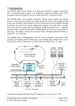
E8-1PPS Series GPS Timing & Frequency Reference
Introduction
The GPS clock is shipped ready for operation. No adjustments are needed to have a 10MHz
frequency reference and 1 pulse per second time reference within 20 minutes of initial switch on.
The status of the GPS lock is shown on four LEDs on the front panel.
For more information as to satellite signal strengths, etc, a computer with RS232 may be connected
to the interface. A program such as NMEA Time may be used to display information from the GPS
receiver.
Installation
The antenna should be installed, preferably with a 360 degree view of the sky. However the
receiver is very sensitive and will give good results with the antenna on a window ledge, or even
inside a building. The satellite signal strengths may be checked after installation using a computer
with suitable software connected to the RS232 interface. The DC power supply should be
connected. The unit will operate with any voltage between 12 and 18V DC. Current consumption
for the E8-X is about 250mA max and the E8-Y/E8-1PPS about 300mA continuous, 600mA
maximum warm up. A universal line power supply is provided.
Operation
The unit is fully programmed to operate without adjustment anywhere in the world. The GPS
receiver will take about 1 minute to obtain a fix from a cold start with unknown location. The
receiver then does a "site survey" for about 15 minutes, averaging the positions obtained. After the
site survey is complete, the receiver switches to position hold mode, and uses all the satellites
available to improve the accuracy of the time calculation. At this point the unit will lock its 20MHz
reference oscillator to the GPS signal. This only takes a few seconds. Desk top: - when the PLL
locks the red "lock" LED should go out, but may flash for a further minute as the PLL settles. The
normal operating condition is with the red "lock" LED off. Rack mount: - when the PLL locks the
“ON” LED will change from amber to green, but may flash amber for a further minute as the PLL
settles. The normal operating condition is with the "ON" LED green.
The status of the satellite tracking is shown by the SATS USED LED. The normal situation is that
the LED shows a long flash, followed by a number of short flashes. The number of short flashes
shows the number of satellites being tracked, and included in the time solution. E8-X Only - the
Lower LED may also flash. This shows the number of satellites being tracked, but not included in
the timing solution. All other variants – the lower LED flashes once every time a 1PPS pulse is
present.
If the red "lock" LED should start to flash at about 1Hz rate, this indicates that the phase error
between the GPS signal and the internal 20MHz oscillator is greater than a pre programmed
threshold. This does not indicate that the 10MHz output is unlocked. During normal operation the
GPS receiver estimates the accuracy of the timing solution using the "TRAIM" algorithm (Time
Receiver Autonomous Integrity Monitoring). If the predicted timing error is greater than the
programmed limit, the receiver will switch into holdover, and the red lock LED will turn on. The
10MHz output and 1PPS output will then drift according to the ambient temperature and aging of
the internal oscillator. The unit should never go into holdover during normal operation. The most
likely reason for doing so is a major antenna fault.
E8-1PPS Series A5 Manual 16 July 2014
Page 6 of 40
Model E8-1PPS Series Operation Manual
GPS interface
The GPS receiver interface uses NMEA format. In order to use this, a freeware program such as
Trimble Studio should be installed on the user’s PC.
Connect the unit to the PC and start the program. It may be necessary to set the port and baud rate
(9600).
The various windows available from the program should show current satellite data, etc.
GPS interface (E8-X NavSync Version Only)
The Internal GPS receiver interface uses Motorola binary format. In order to use this, a freeware
program such as WinOncore should be installed on the user’s PC.
Connect the unit to the PC and start the program. It may be necessary to set the port and baud rate
(9600). The receiver is preset to output 3 sentences on a continuous basis. These are Ha,
(position/status/data), Hn, (12 channel TRAIM status message) and Bb (Visible satellites).
The various windows available from the program should show current satellite data, etc.
It is important to note that some parameters shown by the program will not correctly indicate the
actual state of the receiver. This is because the program does not automatically update its
information when started. In particular, the TRAIM algorithm will be shown as off when in fact it is
by default on in the receiver.
For the receiver to operate correctly, the site survey must be enabled, and the TRAIM must be on. If
this is not the case, the receiver will track satellites and compute a fix, but the red lock LED will
not go out, showing the 10MHz output is in the standby state.
If the receiver gets stuck in a state where it does not lock, the user may inadvertently disabled the
TRAIM or the site survey. To get back to a known state, the following should be performed:
The messages can be sent using the message window in the WinOncore software.
Return to factory default state:
“@@Cf”
Enable Position Auto-survey; consult the CW12 user manual for further details.
“@@Gd03”
Enable T-RAIM algorithm; consult the CW12 user manual for further details.
“@@Ge01”
Enable 1PPS output when >1 satellite is being tracked; consult the CW12 user manual for further
details.
“@@Gc02”
Set the alarm threshold for the T-RAIM algorithm (300ns). Consult the CW12 user manual for
further details.
“@@Gf0003”
Request channel T-RAIM status message (sent every second).
“@@Hn01”
If required, the position/status/data message may be turned on:
“@@Ha01”
E8-1PPS Series A5 Manual 16 July 2014
Page 7 of 40
Model E8-1PPS Series Operation Manual
If required, the visible satellites message may be switched on:
“@@Bb01”
The GPS receiver stores the current status in non volatile memory when switched off.
Microcontroller Interface (E8-1PPS & E8000-TT/E8000A Only)
The microcontroller interface allows setup and debug of the digital phase lock loop which locks the
20MHz reference oscillator to the GPS receiver. The list of control codes is given in an appendix.
Network Time Protocol Time Server Output
The NTP Time server output provides a simple method of putting accurate time information onto a
network. In order to use this, a freeware program such as Tardis 2000 should be installed on the
user’s PC.
Connect the unit to the PC and start the program. It may be necessary to set the port and baud rate
(9600).
NMEA Messages
There are two main types of sentence, ‘Approved’ and ‘Proprietary’. All sentences start with $
delimited with commas and ending with <CR><LF>. Approved sentences are recognized by the
first 5 characters after the $, which define both the kind of talker providing the information (2
characters, GP in the case of a GPS), and the type of information (3 characters). Proprietary
sentences are indicated by a P following the $, as the first of the 5 characters, the next 3 indicating
the manufacturer (from a listing of mnemonic codes), and the 5th character being selected by that
manufacturer for the particular sentence structure. Proprietary sentences must conform to the
general NMEA structures, but are otherwise undefined outside of the Manufacturers own
documentation.
The following Approved messages are available from the receiver:
GPGLL - Geographic Position - Latitude longitude
GPGGA - Global Positioning System Fix Data
GPGSA - GNSS DOP and Active Satellites
GPGSV - GNSS Satellites in View
GPRMC - Minimum required sentence
GPGLL - Geographic position, Lat/Lon
Latitude and longitude, with time of position fix and status.
$GPGLL, Latitude, N, Longitude, E, hhmmss.sss, Status, Mode*cs
$GPGLL
Latitude
N
Longitude
E
hhmmss.sss
Status
Mode
cs
NMEA sentence header (Position Data)
User datum latitude degrees, minutes, decimal minutes format (ddmm.mmmmmm)
Hemisphere ‘N’ = North, or ‘S’ = South
User datum longitude degrees, minutes, decimal minutes format (dddmm.mmmmmm)
Longitude Direction ‘E’ = East, or ‘W’ = West
UTC Time in hours, minutes, seconds and decimal seconds format.
Status V = navigation receiver warning, A = data valid
Mode indicator: A = Valid, Autonomous, D = Valid, Differential, E = Invalid, Estimated, N
= Invalid, Not valid
Message checksum in hexadecimal
GPGGA - GPS fix data
Time and position, together with GPS fixing related data.
E8-1PPS Series A5 Manual 16 July 2014
Page 8 of 40
Model E8-1PPS Series Operation Manual
$GPGGA, hhmmss.sss, Latitude, N, Longitude, E, FS, NoSV, HDOP, Altref, M, msl, M,
DiffAge, DiffStation*cs
$GPGGA
hhmmss.sss
Latitude
N
Longitude
E
FS
NoSV
HDOP
AltRef
M
msl
M
DiffAge
DiffStation
cs
NMEA sentence header (Position Data)
UTC Time in hours, minutes, seconds and decimal seconds format.
User datum latitude degrees, minutes, decimal minutes format (ddmm.mmmmmm)
Hemisphere ‘N’ = North, or ‘S’ = South
User datum longitude degrees, minutes, decimal minutes format (dddmm.mmmmmm)
Longitude Direction: ‘E’ = East, ‘W’ = West
Fix Status: 0 No fix 1 Standard GPS 2 Differential GPS
Number of satellites used in the position solution
2-D Horizontal Dilution of Precision (0.00 to 99.99)
Altitude (metres) above user datum ellipsoid
Units of height (metres)
Mean Sea Level
Units of Mean Sea Level (meters)
Age of differential correction
Differential base station ID
Message checksum in hexadecimal
GPGSA - GPS DOP and Active satellites
GPS receiver operating mode, satellites used for navigation and DOP values.
$GPGSA, Smode, FS, sv, sv, sv, sv,,,,,,,, PDOP, HDOP, VDOP*cs
$GPGSA
Smode
FS
sv
PDOP
HDOP
VDOP
cs
NMEA sentence header (Satellite Data)
A = Automatic switching 2D/3D M = Manually fixed 2D/3D
Fix Status: 1 No fix 2 2D GPS Fix 3 3D GPS Fix
Satellites in use, null for unused fields (12 available fields)
3-D Position Dilution of Precision (0.00 to 99.99)
2-D Horizontal Dilution of Precision (0.00 to 99.99)
Vertical Dilution of Precision (0.00 to 99.99)
Message checksum in hexadecimal
GPGSV - GPS Satellites in View
The number of satellites in view, together with each PRN, elevation and azimuth, and C/No
value. Up to four satellite details are transmitted in one message, with up to three messages
used as indicated in the first field.
$GPGSV, NoMsg, MsgNo, NoSv{ ,sv, elv, az, cno}{, sv, elv, az, cno….}*cs
Note: {} designate optional sections that appear only if there is satellite data.
$GPGSV
NoMsg
MsgNo
NoSv
sv
elv
az
cno
cs
NMEA sentence header (Satellite Data)
Total number of GPGSV messages being output
Number of this messages
Number of satellites in view
Satellites ID
Satellite elevation angle (degrees)
Satellite azimuth angle (degrees)
Satellite signal/Noise ratio (dB/Hz)
Message checksum in hexadecimal
GPRMC - Recommended Minimum data
The ‘Recommended Minimum’ sentence is defined by NMEA for GPS/Transit system data.
$GPRMC, hhmmss.sss, status, latitude, N, Hemisphere, longitude, E, spd, cmg, ddmmyy,
mv, mvd, Mode*cs
$GPRMC
hhmmss.sss
status
Latitude
NMEA sentence header (Recommended Minimum Sentence)
UTC Time in hours, minutes, seconds.
Status: V = navigation receiver warning, A = data valid
User datum latitude degrees, minutes, decimal minutes format (ddmm.mmmmmm)
E8-1PPS Series A5 Manual 16 July 2014
Page 9 of 40
Model E8-1PPS Series Operation Manual
N
Longitude
E
spd
cmg
ddmmyy
mv
mvd
Mode
cs
Hemisphere: ‘N’= North, or ‘S’ = South
User datum longitude degrees, minutes, decimal minutes format (dddmm.mmmmmm)
Longitude Direction: ‘E’ = East, ‘W’ = West
Speed over ground (knots).
Course made good
Date in Day, Month Year format
Magnetic variation
Magnetic variation direction
Mode Indicator: D = Valid, Differential, A = Valid, Autonomous, E = Invalid, Estimated, N
= Invalid, Not Valid
Message checksum in hexadecimal
GPS and Windows Serial Mouse Issue
Problem: It is possible for windows to incorrectly interpret the data output from the Quartzlock GPS
interface as the output of a Microsoft Serial BallPoint Mouse. When that happens, Windows loads
drivers for the Serial BallPoint Mouse. This causes the cursor to move erratically about the display,
clicking, right clicking, double clicking, dragging and dropping display items as it goes. On
Windows 2000, XP and Vista, you may not experience the problem if you wait until after the
computer is booted before connecting the Quartzlock GPS to the serial communications port. This
problem is not specific to Quartzlock GPS. Any NMEA/Binary output device connected to a
Windows computer’s serial port is likely to cause this problem. Below are several possible
solutions to this problem.
Solution 1:
The easiest solution is to disable the Serial BallPoint mouse in the Device Manager. Of course, this
solution assumes that you do not need to use a Serial BallPoint mouse with your computer. When
the wild mouse problem occurs follow the steps below.
1. Unplug the DB9 connector.
2. Right click the My Computer icon on your desktop and select Properties to open the
Device Manager.
3. Go to the hardware tab of the resulting pop up window and click on the Device Manager
button.
4. Right click on Serial BallPoint Mouse and choose the option to Disable (NOT uninstall)
this device.
Solution 2:
Do not plug the DB9 connector into the computer until the computer is turned on and the operating
system is completely booted and running. Every time you use the Quartzlock GPS, you will need to
start the computer and operating system before making the connection between the Quartzlock GPS
and the computer. This solution normally works on Windows 2000, XP and Vista computers.
E8-1PPS Series A5 Manual 16 July 2014
Page 10 of 40
Model E8-1PPS Series Operation Manual
Specifications
OUTPUTS:
Sine wave, 10MHz, 12dBm ± 2dBm into 50ohms
Harmonics
< -50dBc
Spurii
< -75dBc
TTL, 3.3V CMOS, 1 Pulse Per Second
POWER SUPPLY:
100 to 240 AC 700mA (Rack Mount)
12 to 15V DC 250mA – 1500mA (Desk Top)
DPLL tracking bandwidths
5mHz to 500mHz typical in 8 binary increments
Default 20mHz
LOCK INDICATOR (Desk Top)
On
not locked
Off
locked, low phase error
Short flash every second:
locked, high phase error
ON INDICATOR (Rack Mount)
Amber
not locked
Green
locked, low phase error
Short amber flash every second:
locked, high phase error
GPS INDICATOR (Desk Top)
SATS USED
indicates no of satellites used in time solution
1PPS
Flashes when 1PPS signal is present
GPS INDICATOR (Rack Mount)
Green
indicates no of satellites used in time solution
Red
Flashes when 1PPS signal is present
INTERFACE
The E8-1PPS has 3 RS232 interfaces
1. NMEA output
JP4 9.6k baud, RS232, 8 bits no parity, no handshake
2. GPS TSIP
JP3 9.6k baud, RS232, 8 bits odd parity, no handshake
3. Microprocessor
JP3 9.6k baud, RS232, 8 bits no parity, no handshake
The E8-X & E8-Y has 1 RS232 interface
1. NMEA output
JP4 9.6k baud, RS232, 8 bits no parity, no handshake
The E8000 has 3 Optional RS232 interfaces
1. NMEA output
E8-1PPS Series A5 Manual 16 July 2014
JP4 9.6k baud, RS232, 8 bits no parity, no handshake
Page 11 of 40
Model E8-1PPS Series Operation Manual
2. GPS TSIP
JP3 9.6k baud, RS232, 8 bits odd parity, no handshake
3. Microprocessor
JP3 9.6k baud, RS232, 8 bits no parity, no handshake
The E8000-TT/E8000A has 3 RS232 interfaces
1. NMEA output
9W D Pins 2 & 4 9.6k baud, RS232, 8 bits no parity, no handshake
2. GPS TSIP
9W D Pins 4 & 9 9.6k baud, RS232, 8 bits odd parity, no handshake
3. Microprocessor
9W D Pins 7 & 8 9.6k baud, RS232, 8 bits no parity, no handshake
INTERFACE CODES
Micro processor codes See Appendix B
E8-1PPS Series A5 Manual 16 July 2014
Page 12 of 40
Model E8-1PPS Series Operation Manual
Appendix A Board Variation/Configuration
TCXO Version
The following components are not fitted: C42
GPS1
R24, R25, R29
TCXO2
U8, U13, U17, U24, U25, U27, U29, U30, U33, U34, U38, U39
VCXO1, VCXO2, VCXO3
Note: - GPS2 WITH internal clock omit U40
GPS2 WITHOUT internal clock fit U40
Link configuration: Link1
Link2
Link3
Link4
Link5
Link6
Link7
Link8
position 2
position 1
position 2
position 2
not used
position 1
open
position 1
OCXO Version without 1PPS holdover and user adjustable 1PPS
The following components are not fitted: C51, C52, C53, C54, C55, C56, C57, C58
GPS2
L2, L3, L4, L5
R39, R40, R41
TCXO1, TCXO2
U13, U17, U24, U25 U27, U28, U29, U30, U33, U38, U39, U40, U41
Link configuration: Link1
Link2
Link3
Link4
Link5
Link6
Link7
position 2
position 1
position 1
position 1
position 2
position 1
short (8V tuning)
OCXO Version with 1PPS holdover and user adjustable 1PPS
The following components are not fitted: C51, C52, C53, C54, C55, C56, C57, C58
GPS2
L2, L3, L4, L5
R39, R40, R41
E8-1PPS Series A5 Manual 16 July 2014
Page 13 of 40
Model E8-1PPS Series Operation Manual
TCXO1, TCXO2
U13, U17, U24, U28, U38, U39, U40, U41
Link configuration: Link1
Link2
Link3
Link4
Link5
Link6
Link7
position 2
position 2
position 1
position 1
position 2
position 1
short (8V tuning)
E8-1PPS Series A5 Manual 16 July 2014
Page 14 of 40
Model E8-1PPS Series Operation Manual
Appendix B µP RS232 control codes
RS232 control codes (all values following command or returned from the microcontroller are hexadecimal unless stated)
* = backed up in EEPROM
OS
Overall Status
OS?
returns overall status bytes:
aa bb cc dd eeee ffff
*
*
*
PO
aa
is test status byte: bits set:
bit0
bit1
bit2
bit3
bit4
bit5
bit6
bit7
50PPS output (default 1PPS)
50PPS input (default 1PPS)
disable auto cal
disable 1PPS output
disable 1PPS input time tag
disable frequency correction (Kalman filter updated)
disable Kalman filter update
disable state control
bb
is lock status byte: bits set:
bit0, 1, 2
bit3
bit4
bit5
bit6
bit7
state (0 to 7)
normalise DACs (cleared automatically)
OCXO warmed up
loop locked
Disable 1PPS quantization correction
zero clock on next 1PPS capture
cc
is output status byte: bits set: bit0
bit1
bit2
bit3, 7
dd
is auto cal byte
(set to FF on loading new firmware)
bit0
set loads EEPROM default 0, then cleared
bit1
set initiates auto OCXO calibration, then cleared
bit2
set when OCXO cal is in progress
bit3
NU
bit4, 7
last EEPROM default number
eeee
is OCXO current
0000 to FFFF
0 to 500mA
ffff
is running time
0000 to FFFF
unit 18.2 hours
OSTaa
write new test status byte
OSLbb
write new lock status byte
OSPcc
write new output 1PPS status byte
OSAdd
write new autocal byte
1PPS base = last input time tag
1PPS base = Kalman phase estimate otherwise 1PPS base is zero
Disable user 1PPS offset calculation(enables PO command)
NU
1PPS OUT
PO?
returns current status of 1PPS output
aa bbbb cc dd
PD
aa
bbbb
cc
dd
modulo50 counter (20ms) range 0 to 49
main counter (400ns) range 0 to 49999 (C34Fh)
delay setting (50ns) range 0 to 8 (delay 50 to 450ns)
vernier (0.25ns) range 0 to 255
POAaa
write new modulo50 counter
POBbbbb
write new main counter
POCcc
write new delay setting
PODdd
write new vernier
1PPS OUT
PD?
returns current user 1PPS offset in decimal ns
(-)aaaaaaaaa
*
(-)aaaaaaaaa
last user 1PPS offset,
PD(space)(string)(carriage return)
TO
-500,000,000 to 499,999,999 ns
inputs new user 1PPS offset in floating point format e.g. to set the offset to 500ns
delay “PD 000000500”
TIMETAG
E8-1PPS Series A5 Manual 16 July 2014
Page 15 of 40
Model E8-1PPS Series Operation Manual
TO?
returns last time tag parameters
aaaaaaaa bbbb cccc dddd ee f(fp string)
PM
aaaaaaaa
bbbb
cccc
dddd
ee
f (floating point)
Last time tag (32 bit)
first capture
second capture
second capture-first capture
Modulo50 capture
last 1PPS quantization correction
TO+
write TO? to command repeat stack
PERFORMANCE MEASURE
PM?
returns last time tag in decimal ns, and other performance indicators
a (fp string) b (fp string) cccccccc dddd eeee f (fp string) g (fp string)
a (floating point)
b (floating point)
cccccccc
ddddd
eeeee
f (floating point)
g (floating point)
Corrected time tag
Last Kalman phase estimate
Mean square measurement error (ns squared) (decimal integer)
Filtered performance indicator 0 to 32768 (decimal integer)
S1 multiplier (decimal integer)
Frequency estimate and correction
Mean of frequency estimate
PM+
write PM? to command repeat stack
Notes:
The performance indicator is the square of the current fractional frequency estimate divided by the P22 element of the error covariance matrix
multiplied by 2048. The normal running value is 0 to 100
The mean square measurement error is the (Kalman phase estimate minus the current time tag) ^2 and filtered in an 8th order exponential
filter. Units are ns^2.
The S1 multiplier is the constant used to multiply the S1 system noise parameter (random walk FM). This results in a recalculation of the Q
matrix (system covariance matrix). This adjusts the filter for expected increased drift rate of the controlled oscillator.
The mean of the frequency estimate is the Kalman frequency estimate filtered by a 5th order exponential filter
KP
Kalman filter error covariance matrix
*
KP?
returns current error covariance matrix
P11
P12
P22
KPxx (space) (string) (carriage return)
KP+
KQ
P13
P23
P33
in floating point format
inputs a new floating point value, where xx identifies matrix element
write KP? to command repeat stack
System covariance matrix
KQ?
returns current system covariance matrix
Q11
Q12
Q22
Q13
Q23
Q33
Note Q matrix is calculated from system noise parameters on reset, and also in states 2, 3 and 5
KX
System state vector
*
KX?
returns current system state vector
X1
X2
X3
Note X1 is current phase estimate, X2 is current frequency estimate, and X3 is current drift estimate
KX+
write KX? to command repeat stack
KS
System noise parameters
*
KS?
returns current system noise parameters
S1
S2
Note S1 is the level of random walk FM noise, and S2 the level of white FM noise. These are fixed parameters that describe the oscillator
being modelled.
KSx (space) (string) (carriage return)
KZ
Measurement parameters
*
KZ?
inputs a new floating point value where x is the matrix element
returns the latest measurement, and the current measurement noise parameter
E8-1PPS Series A5 Manual 16 July 2014
Page 16 of 40
Model E8-1PPS Series Operation Manual
Z (Corrected)
Timetag
Correction
R
Note Z is the last measurement in seconds; Timetag is the uncorrected Timetag in ns; Correction is the quantization correction decoded from
the GPS receiver in ns. R is the expected variance of the measurement noise in seconds squared.
KZ1 (space) (string) (carriage return)
inputs a new R
KZ+
write KZ? to command repeat stack
OC
Oscillator control parameters
*
OC?
returns latest oscillator control constant and maximum tuning voltage
OC1
OC2
Note OC1 is oscillator tuning constant in fractional frequency /volt, and OC2 is the maximum tuning voltage in volts, assumed 0V
minimum.
OCx (space) (string) (carriage return)
OT
inputs new OC1 or OC2 where x is the parameter
Oscillator tuning control
OT?
returns tuning word and DAC values
aaaaaa bbbb cccc
*
CA
aaaaaa
bbbb
cccc
24 bit tuning word
coarse tuning DAC value
fine tuning DAC value
OTTaaaaaa
inputs new tuning word
OT+
writes OT? to command repeat stack
Auto cal parameters
CA?
returns auto cal parameters
aaaa bbbb cccc dddd
aaaa
bbbb
cccc
dddd
filtered CAL100ns value
filtered CAL500ns value
last CAL100ns value
last CAL500ns value
EU
EEPROM update (backed up values from RAM)
ED
load EEPROM and RAM with default values
EDa
loads EEPROM with default a
a=0
a=1, 2....9
SR
Software Reset
ER
EEPROM read
EW
default automatically loaded after new firmware
parameters for other oscillator types (defined in firmware)
ERCaaaabb
returns bb bytes from starting address aaaa as ASCII characters
ERNaaaabb
returns bb bytes from starting address aaaa as hexadecimal numbers (character pairs)
EEPROM write
EWCaaaabbccccc------c
writes bb characters to starting address aaaa. Correct number of characters must be included in string
EWNaaaabbcccc------c
Writes bb bytes to starting address aaaa. Character pairs cc etc are interpreted as hexadecimal numbers.
DR
Dump RAM
DRaaaabb
WF
returns bb bytes from starting address aaaa as hexadecimal numbers (character pairs)
Write Flash Memory
WF
RF
Not Used
Read Flash Memory
RF
RI
Not Used
Repeat Interval
RI?
returns command repeat interval
aa
E8-1PPS Series A5 Manual 16 July 2014
Page 17 of 40
Model E8-1PPS Series Operation Manual
aa
8 bit command repeat interval multiplier. Range 1 to 255. Command repeat interval is 40ms x aa
RI0aa
write new command repeat interval
RID
cancel command repeat and clear command repeat stack
E8-1PPS Series A5 Manual 16 July 2014
Page 18 of 40
Model E8-1PPS Series Operation Manual
Appendix C NMEA 0183 Protocol
This appendix provides a brief overview of the NMEA 0183 protocol, and describes both the
standard and optional messages offered.
Introduction
NMEA 0183 is a simple, yet comprehensive ASCII protocol which defines both the communication
interface and the data format. The NMEA 0183 protocol was originally established to allow marine
navigation equipment to share information. Since it is a well established industry standard, NMEA
0183 has also gained popularity for use in applications other than marine electronics.
For those applications requiring output only from the GPS receiver, NMEA 0183 is a popular
choice since, in many cases, an NMEA 0183 software application code already exists. The E8-1PPS
is available with firmware that supports a subset of the NMEA 0183 messages: GGA, GLL, GSA,
GSV, RMC, VTC, and ZDA.
NMEA 0183 communication interface
NMEA 0183 allows a single source (talker) to transmit serial data over a single twisted wire pair to
one or more receivers (listeners). The table below lists the standard characteristics of the NMEA
0183 data transmissions.
Signal NMEA Standard
Baud rate 9600
Data bits 8
Parity None (Disabled)
Stop bits 1
NMEA 0183 message structure
The NMEA 0183 protocol covers a broad array of navigation data. This broad array of information
is separated into discrete messages which convey a specific set of information. The entire protocol
encompasses over 50 messages, but only a sub-set of these messages apply to the E8-1PPS GPS
receiver. The NMEA message structure is described below.
$IDMSG,D1,D2,D3,D4,.......,Dn*CS[CR][LF]
$
Signifies the start of a message
ID
The talker identification is a two letter mnemonic which describes the source of the
navigation information. The GP identification signifies a GPS source.
MSG The message identification is a three letter mnemonic which describes the message
content and the number and order of the data fields.
,
Commas serve as delimiters for the data fields.
Dn
Each message contains multiple data fields (Dn) which are delimited by commas.
*
The asterisk serves as a checksum delimiter.
CS
The checksum field contains two ASCII characters which indicate the hexadecimal
value of the checksum.
[CR][LF] The carriage return [CR] and line feed [LF] combination terminate the message.
E8-1PPS Series A5 Manual 16 July 2014
Page 19 of 40
Model E8-1PPS Series Operation Manual
NMEA 0183 messages vary in length, but each message is limited to 79 characters or less. This
length limitation excludes the "$" and the [CR][LF]. The data field block, including delimiters, is
limited to 74 characters or less.
Field definitions
Many of the NMEA date fields are of variable length, and the user should always use the comma
delineators to parse the NMEA message date field. The following table specifies the definitions of
all field types in the NMEA messages supported by the E8-1PPS:
Status
A
Single character field: A=Yes, data valid, warning flag clear V=No, data invalid, warning flag set
Special Format Fields
Latitude
llll.lll
Fixed/variable length field: Degreesminutes.decimal-2 fixed digits of degrees, 2 fixed digits of minutes
and a variable number of digits for decimal-fraction of minutes. Leading zeros always included for
degrees and minutes to maintain fixed length. The decimal point and associated decimal- fraction are
optional if full resolution is not required.
Longitude
yyyyy.yyy
Fixed/Variable length field: Degreesminutes.decimal-3 fixed digits of degrees, 2 fixed digits of
minutes and a variable number of digits for decimal-fraction of minutes. Leading zeros always
included for degrees and minutes to maintain fixed length. The decimal point and associated decimalfraction are optional if full resolution is not required.
Time
hhmmss.ss
Fixed/Variable length field: hoursminutesseconds.decimal-2 fixed digits of minutes, 2 fixed digits of
seconds and a variable number of digits for decimal-fraction of seconds. Leading zeros always
included for hours, minutes, and seconds to maintain fixed length. The decimal point and associated
decimal-fraction are optional if full resolution is not required.
Defined
Some fields are specified to contain pre-defined constants, most often alpha characters. Such a field is
indicated in this standard by the presence of one or more valid characters. Excluded from the list of
allowable characters are the following that are used to indicated field types within this standard: "A",
"a", "c", "hh", "hhmmss.ss", "llll.ll", "x", "yyyyy.yy"
Numeric Value Fields
Variable
x.x
Variable length integer or floating numeric field. Optional leading and trailing zeros. The decimal
point and associated decimal fraction are optional if full resolution is not required (example:
73.10=73.1=073.1=73).
Fixed HEX
hh
Fixed length HEX numbers only, MSB on the left
Fixed Alpha
aa
Fixed length field of upper-case or lower-case alpha characters.
Fixed Number
xx
Fixed length field of numeric characters
Information Fields
NMEA 0183 message options
The E8-1PPS can output any or all of the messages listed in the table below. Typically NMEA messages are output at a 1 second interval with the "GP"
talker ID and checksums. These messages are output at all times during operation, with or without a fix.
GGA
GPS fix data
GLL
Geographic position Latitude/Longitude
GSA
GPS DOP and active satellites
GSV
GPS satellites in view
RMC
Recommended minimum specific GPS/Transit data
VTG
Track made good and ground speed
ZDA
Time and date
E8-1PPS Series A5 Manual 16 July 2014
Page 20 of 40
Model E8-1PPS Series Operation Manual
Appendix D TSIP Protocol
Please refer to the Trimble Website
Resolution SMT GG - User Guide
Trimble VTS Software
E8-1PPS Series A5 Manual 16 July 2014
Page 21 of 40
Model E8-1PPS Series Operation Manual
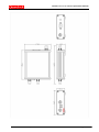
Appendix E Connector, Jumper and Link References
CONN1
External 1PPS Input (MCX)
CONN2
GPS Antenna Input (BNC) (Optional TNC)
CONN3
GPS Antenna Input (SMA) (not fitted if CONN3 fitted)
CONN4
1PPS Output (BNC)
CONN5
1PPS Output (MCX) (not fitted if CONN4 fitted)
CONN6
10MHz RF Output Sine/Square (MCX/SMA) (not fitted if CONN7 fitted)
CONN7
10MHz RF Output Sine/Square (BNC)
CONN8
External 10MHz RF Input (MCX/SMA)
J1
Lumberg 1613 14
15Vdc Input
JP2
Samtek TSM-103-01-S-DV
Pin 1 – External reference tune output
Pin 2 – External reference lock input
Pin 3 – Ground
Pin 4 – Ground
Pin 5 – Not Connected
Pin 6 – Not Connected
JP3
Samtek TSM-104-01-S-DV
Pin 1 – Ground
Pin 2 – Ground
Pin 3 – GPS Port A RS232 RX
Pin 4 – uP RS232 RX
Pin 5 – GPS Port A RS232 TX
Pin 6 – uP RS232 TX
Pin 7 – Loopback
Pin 8 – 1PPS Output (Holdover Option)
JP4
TE Connectivity 5747840-6
Pin 1 – Not Connected
Pin 2 – GPS Port B RS232 RX
Pin 3 – GPS Port B RS232 TX
Pin 4 – Not Connected
Pin 5 – Ground
Pin 6 – Not Connected
Pin 7 – Not Connected
Pin 8 – Not Connected
Pin 9 – Not Connected
JP5
Eeprom programming connection
Link1
Select 1PPS input: Link Position 1 – External 1PPS input via CONN1
Link Position 2 – Onboard GPS 1PPS input
2
C
1
Link2
Select 1PPS Output (CONN4 / CONN5): Link Position 1 – Onboard GPS 1PPS Direct Output (No Holdover)
Link Position 2 – 1PPS smoothed output (Holdover)
E8-1PPS Series A5 Manual 16 July 2014
Page 22 of 40
Model E8-1PPS Series Operation Manual
Link3
Select controlled oscillator type: Link Position 1 – OCXO / EXT
Link Position 2 – TCXO
Link4
Select controlled oscillator type: Link Position 1 – OCXO / EXT
Link Position 2 – TCXO
Link5
Select controlled oscillator input: Link Position 1 – External input via CONN8
Link Position 2 – Onboard oscillator
Link6
Select 10MHz output (CONN6 / CONN7): Link Position 1 – Sine wave output
Link Position 2 – Square wave output
Link7
Open for 5V oscillator tuning link for 8V oscillator tuning voltage
Link8
Select TCXO supply voltage: Link Position 1 – 3.3Vdc
Link Position 2 – 5Vdc
TP1
1PPS Input
TP2
OCXO tuning control voltage output
TP3
1PPS Output
TP4
TBC
TP5
Test Out
TP6
Capture
TP7
TBC
TP8
OCXO current monitor
TP9
+15Vdc
TP10
Ground
TP11
External Reference Oscillator Lock Input (High +5Vdc = Not Locked. Low 0Vdc = Locked)
E8-1PPS Series A5 Manual 16 July 2014
Page 23 of 40
Model E8-1PPS Series Operation Manual
TP12
Lock LED
TP13
1PPS (GPS1 fitted) or SATS Unused LED (GPS2 fitted)
TP14
SATS Used LED
TP15
ON LED
TP16
+5Vdc
TP17
+5Vdc Ref
TP18
+10Vdc
TP19
+3.3Vdc
TP20
GPS2 site survey finished
E8-1PPS Series A5 Manual 16 July 2014
Page 24 of 40
Model E8-1PPS Series Operation Manual
Appendix F EEPROM defaults
DEFAULT 0 OCXO medium performance with 0 to 5V tuning
Automatically loaded after programming firmware
S1 = 2E-12
S2 = 3E-11
Rmeas = 225E-18
OSCcontrolconstant = 2E-7
OSCtunespan = 5.0
maxphasedrift0 = 20000
(in nanoseconds)
DEFAULT 1 OCXO medium performance with 0 to 8V tuning
S1 = 2E-12
S2 = 3E-11
Rmeas = 225E-18
OSCcontrolconstant = 2E-7
OSCtunespan = 8.0
maxphasedrift0 = 20000
(in nanoseconds)
DEFAULT 2 TCXO low performance with 0 to 3.3V tuning, NavSync receiver
S1 = 2E-11
S2 = 3E-10
Rmeas = 2.5E-15
OSCcontrolconstant = 5E-6
OSCtunespan = 3.3
maxphasedrift0 = 200000
(in nanoseconds)
DEFAULT 3 Rubidium high performance with 0 to 5V tuning
S1 = 2E-14
S2 = 5E-12
Rmeas = 225E-18
OSCcontrolconstant = 0.4E-9
OSCtunespan = 5.0
maxphasedrift0 = 5000
(in nanoseconds)
DEFAULT 4 TCXO low performance with 0 to 3.3V tuning, Trimble receiver
S1 = 2E-11
S2 = 3E-10
Rmeas = 2.5E-15
OSCcontrolconstant = 5E-6
OSCtunespan = 3.3
maxphasedrift0 = 200000
(in nanoseconds)
Notes: - default is loaded using EDx command, where x is default number.
After loading a default, software will attempt to calibrate the actual tuning slope (control constant)
of the oscillator. Lock state must be 4 for this to occur.
E8-1PPS Series A5 Manual 16 July 2014
Page 25 of 40
Model E8-1PPS Series Operation Manual
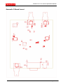
Appendix G Board Layout
E8-1PPS Series A5 Manual 16 July 2014
Page 26 of 40
Model E8-1PPS Series Operation Manual
E8-1PPS Series A5 Manual 16 July 2014
Page 27 of 40
Model E8-1PPS Series Operation Manual
Appendix H Instrument RS232 Connections 9 Way Male Connector
E8-X, E8-Y, E8000, E8010
Pin
1.
2.
3.
4.
5.
6.
7.
8.
9.
N/C
RS232 RX NMEA Data
RS232 TX NMEA Data
N/C
Ground
N/C
N/C
N/C
N/C
E8-X, E8-Y, E8000, E8010 TSIP Option
Pin
1.
2.
3.
4.
5.
6.
7.
8.
9.
N/C
RS232 RX TSIP
RS232 TX TSIP
N/C
Ground
N/C
N/C
N/C
N/C
E8000-TT/E8000A
Pin
1.
2.
3.
4.
5.
6.
7.
8.
9.
N/C
RS232 RX GPS NMEA Data
RS232 TX GPS NMEA Data
RS232 RX Data Trimble TSIP
Ground
N/C
RS232 RX E8-Series Micro Controller
RS232 TX E8-Series Micro Controller
RS232 TX Data Trimble TSIP
E8-1PPS Series A5 Manual 16 July 2014
Page 28 of 40
Model E8-1PPS Series Operation Manual
Appendix I Board Test
Introduction
This board locks an oscillator (TCXO, OCXO or rubidium oscillator) to a 1PPS pulse stream from
an integrated GPS receiver. The hardware comprises a number of more or less independent sections
which require testing on each new board.
The circuit sections are:
a)
b)
c)
d)
e)
f)
1PPS output circuit
1PPS time tag circuit
Controlled oscillator tuning supply
GPS module and interfaces
Controlled oscillator
Options
The design uses a PIC 18F65K22 microcontroller which is clocked at 10MHz from the controlled
oscillator. This ensures the microcontroller internal clock is synchronous with the controlled
oscillator. By time tagging the incoming 1PPS using the internal clock, the frequency difference
between the 1PPS input and the controlled oscillator can be measured. Frequency corrections are
then made to the controlled oscillator.
The board test uses special test routines that are a permanent part of the operating software.
General purpose test equipment is used to make manual measurements.
Circuit Descriptions
1PPS output circuit
This part of the circuit is only fitted if an E8-1PPS is built with optional 1PPS holdover
The microcontroller generates a rising edge on pin 3(ECCP3). This is generated using an internal
peripheral (capture/compare module) when the internal clock equals the setting of the 1PPS output
delay register. The delay register is settable by the PD command.
The internal resolution of this edge is 400ns (One processor cycle at a clock frequency of 10MHz).
In order to provide 1ns delay resolution, the rising edge is further delayed by the shift register U25
and the analogue delay chip U30. U25 shifts the rising edge into the shift register on each selectable
rising or falling edge of the processor clock (exclusive OR gate U29 provides the clock inversion).
Each output of the shift register provides a delayed and re-clocked rising edge with successive
delays of 100ns. Inversion of the clock shifts all the delayed outputs by 50ns. U27 is a 16 to 1
multiplexer that selects one of the edges under control of the 4 bit address provided by the
microcontroller. Bit 0 of the address is used to invert the clock. Bits 1 to 3 are used to select the
delayed edge. The minimum delay is 50ns, and the maximum used is 450ns.
The output on pin 5 of U27 is then applied to U30. U30 is a standalone delay chip that provides
delay increments of approximately 0.25ns steps from 0 to 63ns. There is a fixed delay of about
20ns.
Using the three delay mechanisms, the processor can calculate appropriate settings to delay the
1PPS output -500000000 to +499999999 ns in 1ns steps.
An internal timer terminates the 1PPS pulse after 10ms.
E8-1PPS Series A5 Manual 16 July 2014
Page 29 of 40
Model E8-1PPS Series Operation Manual
1PPS time tag circuit
This is the most complicated of the three circuit blocks.
It can time tag the incoming 1PPS rising edge to a resolution of 1ns. It does this by a combination
of an internal capture module, (ECCP2) and a pulse width expander. After the first 1PPS, the
processor has a near exact knowledge of when the next and subsequent 1PPS edges will arrive. It
prepares for a new edge by setting the ready line (pin 48) high. This will occur between 20 and
40ms before the next 1PPS edge.
Initially D types U4A, U4B, U9A, and U9B are reset. Multiplexer U3 is configured to pass the
incoming 1PPS to the clock input of U4A, so the 1PPS edge will set U4A. The processor pin 40
(CLKO) has a square wave at 2.5MHz, synchronized to the processor internal cycle clock. The first
falling edge of CLKO will set U4B (clock is inverted by U11). The next rising edge of the 10MHz
clock will then set U9A.
When U9A Q goes high, an internal capture is generated in the processor via OR gate U12 and the
ECCP2 input pin. This capture provides an internal hardware read of the internal clock register.
As the 1PPS input is asynchronous, the time between the setting of U4A and U4B will vary between
0ns and 400ns depending on the phase of the 1PPS relative to the processor internal cycle clock.
U9A is always set 100ns after U4B. And gate U15 generates a pulse between 100ns and 500ns by
anding the Q output of U4A, and the ~Q output of U9A. This is applied to the gate of TR1 which
charges the integrator an amount which depends on the pulse width.
In the resting state the integrator U14 is stabilised by feedback through U10. A bias voltage of 2.0
volts is applied to pin 4 of U10. The integrator positive input (pin 3, U14) is connected to 2.5V
derived from a potential divider from the +5V reference. Current flows to the negative input
through R10, and then to the output of U10 through D2 and R11. The positive input of U10 is
connected to the integrator output through R12. The effect is to stabilise the integrator output
voltage at 2.0 volts.
When a 1PPS pulse arrives, U9B is set. This applies a higher positive voltage to U10 positive input
via R15 and D3.The output of U10 goes high, and reverse biases D2, effectively disconnecting the
stabilisation circuit from the integrator. The pulse to be expanded, length 100 to 500ns, turns on
TR1. The integrator charges due to current in R13 to an output voltage between 3V and 8V
depending upon the pulse width. After TR1 turns off, the integrator discharges due to current in
R14. This discharge is about 2000 times slower than the charge rate, which expands the input pulse
to a time between 200us and 1ms.
The positive input of the fast comparator U5 is biased at 1.9V. When the integrator output voltage
falls to this level, the output of U5 goes high, generating a second capture via OR gate U12. The
processor can measure the time between the 2 captures with a resolution of 400ns. Because of the
2000 times expansion of the integrator, the basic resolution is 200ps.
When the comparator output goes high, U9B is reset via U7, reconnecting the stabilization circuit
ready for the next expansion.
Calibration
The pulse expander is an analogue circuit which can drift. It needs calibration so the range of the
expanded pulse can be exactly referred to the 100 to 500ns unexpanded pulse. The calibration
operates by generating pulses of exactly 100ns wide and 500ns wide by gating the 10MHz clock.
These calibration pulses are expanded and measured. The results can then be used to correct
measurements of the 1PPS input.
E8-1PPS Series A5 Manual 16 July 2014
Page 30 of 40
Model E8-1PPS Series Operation Manual
The calibration operates every 20ms when the 1PPS input is not expected. Each calibration cycle
generates a pulse of 100ns and 500ns which are measured. If the CAL_ON line on pin 47 of the
processor is set high before the READY line is set high, gate U3 routs the clock input of U4A to the
(inverted) CLKO line. This makes the D type chain generate the calibration pulse. The 500/100ns
line and gate U18 controls the width of the calibration pulse. The processor averages the calibration
readings in a long time constant filter. The filtered results are used to correct each 1PPS timetag.
Controlled oscillator tuning supply
The controlled oscillator supply is nearly identical to that used in the A6-CPS. A dual 16bit DAC is
used to generate a tuning voltage in the range 0 to 5V. The fine tune DAC output is divided by 256
and added to the output of the coarse tune DAC. There is provision for two different dual DACs to
be fitted. U23 is a lower cost option, and U24 is lower noise for use with the lowest phase noise
OCXOs. U21 provides DC gain to increase the maximum tuning voltage to about 8V. Two tuning
voltage ranges are provided, 0 to 5V with link7 open, and 0 to 8V with link7 closed.
GPS receiver and interfaces
Provision is made for either a Trimble Resolution-SMT or a NavSync CW25-TIM GPS receiver to
be fitted. It is intended that the Resolution-SMT (GPS1) should be used in all builds of the E81PPS. The CW25-TIM (GPS2) can be used in builds of the E8(X)-1PPS. Two versions of the
CW25 can be used, with or without internal TCXO clock.
Each GPS receiver has two serial ports. The default for GPS1 is that port A is TSIP binary. This
must not be changed, as the microcontroller monitors packets on this interface. Port B can be set to
either TSIP or NMEA as covered in the board setup described later. Port A is connected to header
JP3 pins 3 (RxD) and pin 5 (TxD). Port B is connected to the 9 way D connector JP4 pins 2 (RxD)
and pin 3 (TxD).
The default for GPS2 is Port 0 is Motorola binary protocol, and Port 1 is NMEA. Port 0 is
connected to JP3, and Port1 to JP4.
The microcontroller interface is connected to JP3 pin 4 (RxD) and pin 6 (TxD)
LED Interface
When GPS1 is fitted, the microcontroller decodes packet 6D which contains the number of
satellites currently used in the over determined time solution. LED1A is flashed to indicate this
number. LED1B is flashed each time a 1PPS pulse is received by the microcontroller. LED2B is the
lock indicator which has a number of flash codes, described later. LED2A is the power on LED
When GPS2 is fitted, R24 and R25 are omitted. R39 and R40 are fitted which connect LED1A and
LED1B directly to the internal LED interface in GPS2. These LEDs then flash to show the number
of satellites tracked, and the number used in the time solution.
Controlled oscillator
The controlled oscillator is intended to be an OCXO in E8-1PPS variants and a TCXO for the
E8(X)-1PPS A rubidium oscillator may also be used.
For OCXO variants, link5 is set to position 2. The OCXO sine output is applied to comparator U31.
The anti-phase square wave outputs are the processor clock, and the 1PPS output circuit clock.
Links 3 and 4 are set to position 1.
For TCXO variants, link8 is set to position 1 for 3.3V supply, and position 2 for 5V supply to the
TCXO. The TCXO frequency is 20MHz, and is applied to comparator U31. U28 divides the TCXO
frequency by 2, and the anti-phase 10MHz signals are selected by links 3 and 4 set to position 2.
E8-1PPS Series A5 Manual 16 July 2014
Page 31 of 40
Model E8-1PPS Series Operation Manual
For rubidium versions, link 5 is set to external 10MHz (position 1). The rubidium output is applied
to CONN8. The rubidium tuning voltage is at pin 1 of connector JP2. Pin 2 of JP2 is a rubidium
locked signal to the processor (active low).
For OCXO variants, U8 is the 12V regulator for the OCXO. U34 provides a current monitor to the
processor analogue input pin 27. OCXO warm-up is detected by a reduction in OCXO current
below a threshold.
Options
Various hardware options are provided for future expansion
Low noise tuning DAC
U23 will normally be fitted. This is a low cost dual 16 bit DAC. For use with the lowest phase noise
OCXOs, U24 may be fitted. This is the lowest noise dual 16bit DAC available.
Traceability memory
U13 is a 1Mbyte flash memory. This may be used to store status data to prove correct locking to
GPS time over an extended period.
Temperature sensor
U39 is a temperature sensor. This is intended for implementation of a more elaborate OCXO
holdover algorithm.
Required Equipment
a)
b)
c)
d)
e)
source 1 10MHz fixed frequency accuracy ± 1E-6 level 1V RMS (EMF) adjustable
DC voltmeter 5 digit resolution
2 channel oscilloscope, preferably digital storage
Frequency counter, capable of time interval measurement with a resolution of at least 1ns.
RF power meter, 50ohm.
Board Set Up.
A new board should be configured by setting various links. These are solder links. Refer to the
build summary document for the various link connections.
It is assumed that a new board is first tested without the controlled oscillator fitted.
Power up the board from a regulated supply set to 15v. Supply current will depend upon build
configuration.
Supply LED (LED1B green) should light.
Programming
Connect the programmer to JP5 and load the latest version firmware. Board power must be on. In
case of problems, check the Vdd supply at C47 (5V ± 0.15V)
Power Supplies
Check:
a)
b)
c)
d)
e)
+10V ± 0.3V at TP18
Vdd 5V ± 0.15V at C47
+5V ± 0.1V at TP16
+12V ± 0.3V at U8 pin3
5V ref +5V ± 5mV at TP17
E8-1PPS Series A5 Manual 16 July 2014
Page 32 of 40
Model E8-1PPS Series Operation Manual
Board Functional Tests
Power down the board
Set the solder links as follows:
OCXO variants:
1. position 1
external 1PPS
2. position 1
1PPS holdover option NOT fitted
position 2
1PPS option fitted
3. position 1
4. position 1
5. position 1
external 10MHz
6. optional
to suit build specification
sine or square 10MHz output
7. To suit OCXO tuning range
8. Not Used
TCXO variants
1. position1
external 1PPS
2. position 1
note that 1PPS holdover option cannot be fitted to TCXO versions
3. position 2
4. position 2
5. position 1
external 10MHz
6. optional to suit build specification
7. open circuit
5V tuning
8. to suit TCXO supply voltage
Connect source 1 to CONN8 and set to 10MHz, 1VRMS (EMF) The processor should now be
clocked from this source.
LED2B (red) should be continuously on. If it is flashing, the processor is not getting an external
clock.
Check U31, U28 (TCXO version), Link3, 4.
Operation of the interface must first be checked. Connect a PC with RS232 to JP3. Only pins 6
(TXD) pin4 (RXD) and pin 2 (ground) need to be connected. Start a general terminal program, set
the interface to 9600baud, 1start bit, no parity, and check that the microcontroller responds to
commands by sending "OS?"
Connect a second RS232 port to JP3. Only pins 5(TXD) pin3 (RXD) and pin 1 (ground) need to be
connected. Start the appropriate GPS control software (This is Trimble GPS Studio or NavSync
WinOncore). The GPS receiver should start operating within a few seconds of power up, and should
communicate with the control program.
The EEPROM must be set to default values using command “EDx” to match the controlled
oscillator type fitted. See Appendix F for EEPROM defaults.
This only needs to be done after reloading the firmware.
If the 1PPS holdover option is not fitted, connect the external 1PPS source to CONN1 at this point.
LED1B should flash at a 1Hz rate. The state should change to S1, and then S2. The board test
E8-1PPS Series A5 Manual 16 July 2014
Page 33 of 40
Model E8-1PPS Series Operation Manual
software should be started when in state 2. DO NOT allow the state to reach S4, and then
commence the OCXO calibration. This cannot be done when an external 1PPS source is being
driven from the E8-1PPS board 10MHz output. If the OCXO calibration does start, send SR
(software reset) to stop it.
The special board test software is started by entering state7. The following command is used:
OSL07
The reply should be "BOARD TEST 0"
In this state all the normal interface commands are locked out except the keys "I" (increment) and
"D" (decrement). In some tests the keys "H" (high) and "L" (low) can also be used.
I and D may be freely used to step from one test to another. The tests may be performed in any
order. Test F will roll over to test 0 when incremented.
TEST 0
1PPS output delay control
THIS TEST CAN ONLY BE USED IF 1PPS HOLDOVER OPTION IS FITTED
Connect oscilloscope channel 1 to TP7 via a divide by ten probe.
Connect channel 2 to TP3 via a divide by 10 probe. Bandwidth of oscilloscope and probes should
be at least 200MHz. Trigger on channel 1. Time base should be single shot sampling.
The rising edge on TP7 is the start marker (zero time) of the internal clock. The delay of the 1PPS
output is checked relative to this marker.
The 1PPS output is switched to 50PPS for this test to provide a faster update rate.
Using the H and L keys, the delay may be stepped in 10ns increments. This should be observed on
the oscilloscope.
The interface will show the current delay (signed decimal), the shift register delay in 50ns steps,
and the delay vernier (hex). The delay vernier is the programming word applied to U30.
Linearity check
Transfer to probes to the counter (set to 1Mohm input impedance)
Set the delay to 0ns. The counter should read a delay close to 0ns. The residual delay can be up to ±
10ns. This is unimportant, and is caused by loading effects on the 1PPS output. Change the delay in
10ns steps until the vernier setting reads a minimum hex value. The delay chip U30 is now set to its
minimum delay. Step the delay in further 10ns steps. Each increment on the counter should be
10±3ns. When the vernier rolls over, the increment on the counter should be 10±5ns.
If there is a substantial jump at the vernier roll over points, the software constant
DELAYLINEBITS_PER_NS can be adjusted. The software must be re-compiled if this is done.
TEST 1
1PPS output delay control
THIS TEST CAN ONLY BE USED IF 1PPS HOLDOVER OPTION IS FITTED
This test is exactly the same as TEST0, except the delay steps are 100ns. This may be useful in
debugging the shift register circuit.
TEST 2
Calibrator check
For this test, a 1PPS source must be connected to CONN1 as otherwise the calibrator will not be
operating. LED1B should be flashing to show that a 1PPS input is present.
The calibrator is enabled, and continuously displays the results over the interface. Four columns are
displayed:
E8-1PPS Series A5 Manual 16 July 2014
Page 34 of 40
Model E8-1PPS Series Operation Manual
Averaged 100ns cal
Averaged 500ns cal
02AE
0B66
last 100ns cal
last 500ns cal
02AF
0B66 (typical values)
The averaged values will slowly approach the spot values due to the long time constant of the filter.
A maximum jitter of ±1 is normal on the spot values.
As a further check on the time expander, an oscilloscope with a divide by 10 probe should be
connected to TP4. Groups of 2 saw tooth ramps should be observed, each group repeating every
20ms. One group should be expanded. The first ramp is the expansion of the 100ns calibration
pulse, and the second is the expansion of the 500ns calibration pulse.
The following voltage measurements should be made using the oscilloscope cursor:
Ramp start voltage:
2.0V ± 0.1V
First ramp peak voltage:
3.0V ± 0.2V
Second ramp peak voltage:
8.0V ± 0.4V
If the voltages are incorrect, there may be an incorrect component around the time expander circuit.
TEST 3
1PPS capture check
NOTE If 1PPS holdover option is not fitted, this test cannot be used directly as the internal 1PPS
source is not available. An external 1PPS source must be used. This must be synchronous with the
processor clock, and must have very low jitter. A spare A6-1PPS board can be used, with the
10MHz input connected to the 10MHz output of the E8-1PPS board under test. The 1PPS input
should be connected to CONN1.
An A6 frequency converter digital board may also be used.
PROCEDURE IF 1PPS HOLDOVER OPTION IS FITTED:
The 1PPS output is used as a pulse generator to test the 1PPS capture. The 1PPS output should be
connected to the 1PPS input .A link should be made between pins 7 and 8 of JP3. This connects the
1PPS output to the time expander input, overriding the 1PPS from the GPS module.
PROCEDURE IF 1PPS OPTION IS NOT FITTED:
Connect synchronous 1PPS input to CONN1
After each pulse the interface will display the 1PPS user delay (signed decimal in ns), followed by
the 5 parameters output by the “TO” command. These are:
Last time tag (decimal ns)
First capture (hex)
Second capture (hex)
Capture difference (hex)
Modulo50 counter (hex)
If channel 2 of the oscilloscope is transferred to TP4, the integrator output may be observed
The Capture difference should show a maximum jitter of ±1, which is ±200ps. The Last time tag is
rounded to the nearest 1ns. The actual value of the Last time tag depends upon the reset point of the
internal clock, and is not significant.
NOTE If 1PPS holdover option is not fitted, following procedure cannot be used as 1PPS source
delay is not adjustable.
As the 1PPS output delay is stepped using the “H” and “L” keys, the time tag should step with the
same 10ns increments. Note that any nonlinearity detected in TEST0 will also appear in this test.
E8-1PPS Series A5 Manual 16 July 2014
Page 35 of 40
Model E8-1PPS Series Operation Manual
The key point to look for is when the first capture changes by integer 1. This represents an overflow
of the time expander, and is the point where a jump in the time tag might be expected if the
calibration was not working correctly.
TEST 4
THIS TEST CAN ONLY BE USED IF 1PPS HOLDOVER OPTION IS FITTED
This test is similar to TEST3; however the rate of the 1PPS output is increased to 50PPS. This
enables an estimate to be made of the jitter in the time expander. The interface shows the first
capture, the second capture, and the capture difference. The jitter in the capture difference is
normally ±1, which is ±200ps.
TEST 5
Coarse tune DAC
In this test the fine tune DAC is set to 0V and the coarse tune DAC is stepped.
Connect the DC voltmeter between TP5 and ground. By using the H and L keys, check that the
voltage can be stepped between 0V and about 4.659V
TEST 6
Fine tune DAC
In this test the coarse tune DAC is set to midrange and the fine tune DAC is stepped.
Connect the DC voltmeter between TP5 and ground. By using the H and L keys, check that the
voltage may be stepped over a total range of about 18.2mV
TEST 7
OCXO current monitor
In this test the OCXO current is continuously displayed. The current monitor can be checked by
connecting a known resistor from the OCXO supply pin to ground.
The OCXO current is displayed as a 2 byte hex number. Full scale is about 500mA. With no
resistor,
i.e. an OCXO current of zero, the maximum offset should be 0600h.
Connect a 120ohm, 1W resistor from an OCXO supply pin (C40) to ground. The current monitor
has a long time constant so at least 30 seconds should be allowed for the reading to stabilise. Note
the reading, convert to decimal, divide by 65536 and multiply by 500. This should be the current in
mA. A typical reading of 33CCh is a current of 101mA. The expected accuracy is only about 10%.
Test 7 is the last programmed test.
OCXO Output Buffer
The OCXO output buffer operates independently of the processor and can be tested as any linear
amplifier. It has an input impedance of 500ohms, and a gain of 1 into a 50 ohm load. 1VRMS at the
input should give 1VRMS (13dBm) into a 50ohm load.
To test set source 1 to 10MHz. Check that the input level at CONN8 is 1V RMS. Use a high
impedance probe for this. Adjust the output level of source 1 if necessary. Connect an RF power
meter to CONN4 or CONN5 and check for 13dBm ± 1dB
The buffer 1dB bandwidth should be at least 2MHz to 40MHz. This can be checked using a
spectrum analyser /tracking generator combination if desired.
This completes the board test.
To exit the board test software, a power on reset must be performed.
Final Board Configuration
The controlled oscillator should be fitted at this stage. Reset link 5 as follows:
OCXO
position 2
E8-1PPS Series A5 Manual 16 July 2014
Page 36 of 40
Model E8-1PPS Series Operation Manual
TCXO
open circuit
Reset link1 to position 2 (1PPS from GPS receiver)
Power up the board with a GPS antenna connected.
GPS Receiver Configuration
The default configuration needs only a few modifications:
Trimble Resolution-SMT:
Adjust using GPS Studio:
1PPS output mode:
set to 1PPS only output if 1 or more satellites tracked
Packet masks:
Set Primary timing packet (8F-AB), Supplemental timing packet (8FAC), and Auto event packets on
Port B:
may be set to NMEA or TSIP as desired
NOTE: After changes the configuration MUST be saved otherwise the unit will return to the previous
settings after power down.
NavSync CW-25-TIM:
Adjust using WinOncore
Run E8.TXT
Send @@Gc02
1PPS on when tracking 1 or more satellites
The Trimble Resolution-SMT will do a self survey when first powered up at a new location. Further
power ups at the same location will not result in a new self survey.
The NavSync CW25-TIM will always perform a self survey on power up.
Controlled Oscillator Auto Calibration
When new firmware is loaded, EEPROM default 0 is automatically loaded. This is an OCXO with
5V tuning. If an alternative controlled oscillator is fitted, then the appropriate EEPROM default
must be loaded.
It is essential that the physical tuning voltage range, adjusted with Link 7, should match the tuning
voltage range stored in the EEPROM, and loaded by the EEPROM default command. This can be
checked using the “OC?” command.
When the EEPROM default is loaded, a flag is set to indicate that OCXO calibration is required.
The software will attempt to get lock on the 1PPS from the GPS receiver in the normal way, going
through states 0, 1 2 and 3. When the normal running state 4 is entered, the software will
immediately enter the special OCXO calibration routine. This is shown by a message over the
interface. The following actions then happen:
a) The Kalman filter frequency correction is stopped
b) The OCXO tuning is offset by about 10% of the total
c) The Kalman frequency estimate is reset to enable rapid acquisition of the new frequency
d) The command “PM?” is written to the command repeat stack to provide user monitoring
Over a period of about 5 minutes, the filter will acquire the new frequency. From knowledge of the
voltage offset applied to the tuning voltage, and the frequency shift that this has produced, the
tuning constant of the oscillator can be calculated as a fractional frequency/volt. This parameter is
E8-1PPS Series A5 Manual 16 July 2014
Page 37 of 40
Model E8-1PPS Series Operation Manual
then written to EEPROM to replace the default tuning constant. The new tuning constant may be
viewed with the “OC?” command.
After the calibration is complete, the unit will go back to state 0 and should lock normally.
State Control
The following information has been copied from the software listing to provide more information
on the state control:
STATE 0
State 0 is the first state after cold start. Red lock LED is permanently on. The state is exited only
when:
a) The rubidium is locked OR
b) The OCXO has warmed up
c) A 1PPS capture has been received
Test for oscillator type (eeprom default) using NavSync CW25 device. In this case state 0 is only
exited; when CW25 has finished its site survey, and set its ready line high.
STATE 1
State 1 is waiting for the internal clock to be reset. A timeout is started. If no clock reset is
acknowledged in 1 second, state 0; is re-entered. Red lock LED is permanently on.
STATE 2
The internal clock has been synchronized on the first 1PPS capture. Red lock LED is permanently
on.
The Kalman filter should now be tracking the incoming 1PPS, although no frequency corrections
are being made.
In this state, and state 3, the Kalman filter is made adaptable to the real behaviour of the system.
The performance measure filteredfreqerror is used to modify the random walk noise parameter
which describes the controlled oscillator. This is S1.
The frequency error is high so the effective filter bandwidth is too narrow to track warm-up drift of
the oscillator. The scaling parameter of S1, (S1scale) which is the random walk FM noise root
variance, normally preset to 1, is increased according to the value of the filtered frequency error
ratio. After each change to S1scale, the Q matrix is recalculated.
This state is exited after 100 successful 1PPS captures and if the frequency drift is less than a
threshold
If captures stop, after a time out state 0 is entered
STATE 3
In this state the Red lock LED flashes rapidly. The error monitor parameter filteredfreqerror is
compared with a threshold, when it is less than the threshold state 4 is entered and the lock light is
switched off
If the 1PPS captures stop for more than 6 seconds, state 0 is entered, also if captures are more than
MAXTIMEOFFSET (20us) from initial capture when clock was reset in this state the Kalman filter
is made adaptive. The frequency error is high so the effective filter bandwidth is too narrow to track
warm-up drift of the oscillator. The scaling parameter of S1, which is the random walk FM noise
root variance, normally preset to 1, is increased according to the value of the filtered frequency
error ratio. After each change to S1scale, the Q matrix is recalculated.
STATE 4
E8-1PPS Series A5 Manual 16 July 2014
Page 38 of 40
Model E8-1PPS Series Operation Manual
The normal running state. If the filteredfreqerror rises above the high threshold loss of lock is
assumed, and state 5 re-entered.
If the captures stop, the holdover state 6 is entered
STATE5
In this state the Red lock LED flashes rapidly. In this state the Kalman filter is made adaptive. The
frequency error is high so the effective filter bandwidth is too narrow to track warm-up drift of the
oscillator. The scaling parameter of S1, which is the random walk FM noise root variance, normally
preset to 1, is increased according to the value of the filtered frequency error ratio. After each
change to S1scale, the Q matrix is recalculated.
If captures stop, holdover state 6 is entered
STATE6
This is the holdover state. The 1PPS capture flag is tested to see if the GPS module has resumed
fixes, and has restored the 1PPS. If so, state 5 is re-entered to restore tracking in the holdover state,
frequency corrections are inhibited automatically as there are no 1PPS captures.
The red lock LED is flashed with 50% mark space ratio.
User Performance Test
THIS TEST CAN ONLY BE USED IF 1PPS HOLDOVER OPTION IS FITTED
A simple performance test may be made without any equipment. The loop back link must be
connected to pins 7 and 8 of JP3. This will over ride the 1PPS from the GPS receiver, with the
internally generated 1PPS. As the 1PPS output and the 1PPS time tag are using the same internal
clock, the Kalman filter will see no frequency offset and no jitter on the 1PPS time tags. The
performance measure and frequency offset displayed using the “PM” command should reach
limiting low values after about 30 minutes.
In order to do this test, the base time of the 1PPS output should be set to “internal clock” using the
command “OSP00”. If the base time is set to “Kalman estimate” or “Last input time tag”
completely random results will occur.
After the command “OSP00”, the EEPROM should be updated with the command “EU”. “SR” may
now be used to perform a software reset.
The quantization correction from the GPS receiver must now be switched off. This can be done by
setting bit 6 of LOCKSTATUS.
“PM+” will then display the performance measures. The software will go through its start up
procedure with the display of successive states ending in state 4. After 30 minutes the performance
figures should be typically:
-1.2000E-08
–1.2017E-08 0000000
00000 00001 -5.8970E-13 -5.8973E-13
Note that the Kalman phase estimate is almost identical to the time tag, the mean square
measurement error is zero, the filtered performance indicator is zero, the S1 multiplier is 1, the last
frequency estimate and the mean frequency estimate is small. This last figure will further reduce
with time.
If the user 1PPS offset is stepped 10ns, the effect on the performance parameters may be seen. A
single phase step will be rapidly tracked out with minimum effect on the frequency.
After this test, reset the 1PPS base to the Kalman estimate by using the command “OSP02”,
followed by “EU”.
E8-1PPS Series A5 Manual 16 July 2014
Page 39 of 40
Model E8-1PPS Series Operation Manual
Quartzlock UK Ltd
Web:
E8-1PPS Series A5 Manual 16 July 2014
www.quartzlock.com
E-mail:
[email protected]
Page 40 of 40