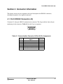
1
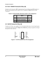
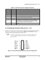
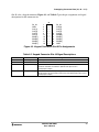
CE - SLK - MMC2001 - A
M•CORE™ STUDENT LEARNING KIT
USER’S MANUAL
Motorola reserves the right to make changes without further notice to any products herein to improve reliability, function
or design. Motorola does not assume any liability arising out of the application or use of any product or circuit described
herein; neither does it convey any license under its patent rights nor the rights of others. Motorola products are not
designed, intended, or authorized for use as components in systems intended for surgical implant into the body, or other
applications intended to support or sustain life, or for any other application in which the failure of the Motorola product
could create a situation where personal injury or death may occur. Should Buyer purchase or use Motorola products for
any such unintended or unauthorized application, Buyer shall indemnify and hold Motorola and its officers, employees,
subsidiaries, affiliates, and distributors harmless against all claims, costs, damages, and expenses, and reasonable
attorney fees arising out of, directly or indirectly, any claim of personal injury or death associated with such unintended
or unauthorized use, even if such claim alleges that Motorola was negligent regarding the design or manufacture of the
part. Motorola and the Motorola logo are registered trademarks of Motorola, Inc. Motorola, Inc. is an Equal
Opportunity/Affirmative Action Employer.
The M•CORE name and logo and the OnCE name are trademarks of Motorola, Inc. CodeWarrior is a registered
trademark of Metrowerks, Inc., a Motorola company.
© MOTOROLA, INC., 2000, 2001; ALL RIGHTS RESERVED
CAUTION: ESD Protection
M•CORE development systems include open-construction printed circuit boards that contain
static-sensitive components. These boards are subject to damage from electrostatic discharge
(ESD). To prevent such damage, you must use static-safe work surfaces and grounding straps, as
defined in ANSI/EOS/ESD S6.1 and ANSI/EOS/ESD S4.1. All handling of these boards must be in
accordance with ANSI/EAI 625.
MOTOROLA
2
MMCSLK2001UM/D
User’s Manual
Contents
Section 1 Introduction
1.1
1.2
1.3
SLK2001 Features . . . . . . . . . . . . . . . . . . . . . . . . . . . . . . . . . . . . . . . . . . . . . . 9
System and User Requirements . . . . . . . . . . . . . . . . . . . . . . . . . . . . . . . . . . . 10
SLK2001 Layout. . . . . . . . . . . . . . . . . . . . . . . . . . . . . . . . . . . . . . . . . . . . . . . 10
Section 2 Configuration
2.1
2.2
2.3
2.4
2.5
Setting the Mode Select Header (W1) . . . . . . . . . . . . . . . . . . . . . . . . . . . . . . 13
Making Computer-System Connections . . . . . . . . . . . . . . . . . . . . . . . . . . . . . 13
Performing the SLK2001 Selftest. . . . . . . . . . . . . . . . . . . . . . . . . . . . . . . . . . 14
Memory Map . . . . . . . . . . . . . . . . . . . . . . . . . . . . . . . . . . . . . . . . . . . . . . . . . 15
Installing Optional Connectors . . . . . . . . . . . . . . . . . . . . . . . . . . . . . . . . . . . . 16
Section 3 Operation
3.1
Debugging Embedded Code . . . . . . . . . . . . . . . . . . . . . . . . . . . . . . . . . . . . . . 17
3.2
Using the SysDS Loader. . . . . . . . . . . . . . . . . . . . . . . . . . . . . . . . . . . . . . . . . 17
3.2.1
Programming FLASH Memory . . . . . . . . . . . . . . . . . . . . . . . . . . . . . . . . . 19
3.2.2
Uploading from FLASH Memory . . . . . . . . . . . . . . . . . . . . . . . . . . . . . . . 20
3.2.3
Verifying FLASH Memory . . . . . . . . . . . . . . . . . . . . . . . . . . . . . . . . . . . . 20
3.2.4
Displaying FLASH Memory . . . . . . . . . . . . . . . . . . . . . . . . . . . . . . . . . . . 21
3.2.5
Erasing FLASH Memory . . . . . . . . . . . . . . . . . . . . . . . . . . . . . . . . . . . . . . 22
3.2.6
Erasing a FLASH Sector . . . . . . . . . . . . . . . . . . . . . . . . . . . . . . . . . . . . . . 22
3.2.7
Blank Checking a FLASH Sector . . . . . . . . . . . . . . . . . . . . . . . . . . . . . . . 22
3.2.8
Restoring System Software . . . . . . . . . . . . . . . . . . . . . . . . . . . . . . . . . . . . 22
Section 4 Connector Information
4.1
4.2
4.3
4.4
Port 0 RS232 Connector (J3) . . . . . . . . . . . . . . . . . . . . . . . . . . . . . . . . . . . . . 25
Port 1 RS232 Connector Site (J4). . . . . . . . . . . . . . . . . . . . . . . . . . . . . . . . . . 26
OnCE Connector Site (J5) . . . . . . . . . . . . . . . . . . . . . . . . . . . . . . . . . . . . . . . 26
Prototyping Connector Sites (J6, J8 — J11). . . . . . . . . . . . . . . . . . . . . . . . . . 27
Index . . . . . . . . . . . . . . . . . . . . . . . . . . . . . . . . . . . . . . . . . . . . . . . . . . . . . . . . . . . . 33
MMCSLK2001UM/D
User’s Manual
3
4
MMCSLK2001UM/D
User’s Manual
Figures
1-1
3-1
3-2
3-3
4-1
4-2
4-3
4-4
4-5
4-6
SLK2001 Evaluation Board . . . . . . . . . . . . . . . . . . . . . . . . . . . . . . . . . . . . . . 11
SysDS Loader Main Screen . . . . . . . . . . . . . . . . . . . . . . . . . . . . . . . . . . . . . . 18
Upload To File Dialog Box . . . . . . . . . . . . . . . . . . . . . . . . . . . . . . . . . . . . . . 20
Display Flash/Ram Display . . . . . . . . . . . . . . . . . . . . . . . . . . . . . . . . . . . . . . 21
OnCE Connector Site J5 Pin Assignments . . . . . . . . . . . . . . . . . . . . . . . . . . . 26
Serial I/O/Reset/Clock Connector Site J6 Pin Assignments. . . . . . . . . . . . . . 27
Keypad Connector Site J8 Pin Assignments. . . . . . . . . . . . . . . . . . . . . . . . . . 29
Address Connector Site J9 Pin Assignments . . . . . . . . . . . . . . . . . . . . . . . . . 30
Data/Control Connector Site J10 Pin Assignments . . . . . . . . . . . . . . . . . . . . 30
PWM/Chip Select Connector Site J11 Pin Assignments . . . . . . . . . . . . . . . . 31
MMCSLK2001UM/D
User’s Manual
5
6
MMCSLK2001UM/D
User’s Manual
Tables
1-1
2-1
2-2
4-1
4-2
4-3
4-4
4-5
4-6
4-7
4-8
SLK2001 Specifications . . . . . . . . . . . . . . . . . . . . . . . . . . . . . . . . . . . . . . . . . 12
SLK2001 Default Memory Map. . . . . . . . . . . . . . . . . . . . . . . . . . . . . . . . . . . 15
FLASH Sector Boundaries . . . . . . . . . . . . . . . . . . . . . . . . . . . . . . . . . . . . . . . 16
Communication Connector J3 (Port 0) Pin Assignments . . . . . . . . . . . . . . . . 25
Communication Connector J4 (Port 1) Pin Assignments . . . . . . . . . . . . . . . . 26
OnCE Connector Site J5 Signal Descriptions. . . . . . . . . . . . . . . . . . . . . . . . . 27
Serial I/O/Reset/Clock Connector Site J6 Signal Descriptions . . . . . . . . . . . 28
Keypad Connector Site J8 Signal Descriptions . . . . . . . . . . . . . . . . . . . . . . . 29
Address Connector Site J9 Signal Descriptions . . . . . . . . . . . . . . . . . . . . . . . 30
Data/Control Connector Site J10 Signal Descriptions . . . . . . . . . . . . . . . . . . 31
PWM/Chip Select Connector Site J11 Signal Descriptions . . . . . . . . . . . . . . 31
MMCSLK2001UM/D
User’s Manual
7
8
MMCSLK2001UM/D
User’s Manual
SLK2001 Features
Section 1 Introduction
This user's manual explains connection, configuration, and operation information for the
CE-SLK-MMC2001-A M•CORE™ Student Learning Kit (SLK2001). This standalone
development tool of Motorola’s M•CORE family lets you develop code to be embedded in an
MMC2001 microcontroller unit.
The SLK2001 lets you use Metrowerks CodeWarrior® software or the Motorola’s System
Development Software (SysDS) Loader to develop and debug your code.
CodeWarrior software is an integrated development environment for writing, compiling, and
debugging assembly, C, or, C++ code. As part of your SLK2001, CodeWarrior software comes
with an academic license and a separate manual.
The SysDS Loader lets you download your code into SLK2001 FLASH memory, for execution or
for storage in non-volatile memory. Section 3 of this manual explains how to use this software.
Your SLK2001 also is compatible with the Mbug debug monitor and with the GNU source-level
debugger. Mbug software is permanently programmed into the MMC2001 resident
microcontroller unit of your SLK2001; the Motorola CD-ROM includes an Mbug manual. The
GNU source-level debugger is available from the Free Software Foundation, at web site
www.GNU.org.
1.1 SLK2001 Features
The SLK2001 features:
•
MMC2001 resident microcontroller unit.
•
256 kilobytes FLASH memory (90-nanosecond access time).
•
256 kilobytes SRAM (10-nanosecond access time).
•
3.3-volt power regulator.
•
An RS232 serial communication port.
•
Address decoding: direct chip select from the processor.
•
CodeWarrior software for M•CORE embedded systems, including a C compiler, an
M•CORE assembler, an M•CORE linker, and the MetroTRK debug monitor.
•
Motorola SysDS Loader development software.
•
Sites for optional, user-supplied connectors:
–
A second RS232 connector,
–
An external battery connector,
MMCSLK2001UM/D
User’s Manual
9
Introduction
–
A 14-pin JTAG/OnCE debug connector,
–
A microcontroller SRAM standby power connector, and
–
Five 20-pin prototyping connectors.
1.2 System and User Requirements
You need an IBM PC or compatible computer, running the Windows 95 or WindowsNT (version
4.0) operating system. The computer requires a Pentium (or equivalent) microprocessor, 16
megabytes of RAM, 50 megabytes of free hard-disk space, an SVGA color monitor, and an RS232
serial-communications port.
To use the SLK2001, you should be familiar with the C programming language.
To see complete results of the SLK2001 selftest, you need Hyperterminal or a comparable
terminal-emulation program.
Your SLK2001 requires a separately purchased, 5-volt power supply. The power-supply cable
must have an 80-mill (2.1 millimeter), center-positive barrel connector. (Factory specialists
recommend 4.75-to-5.25-volt input power, at 25 milliamperes. But the SLK2001 may function
with input power as low as 3.5 volts, or as high as 9 volts.)
1.3 SLK2001 Layout
Figure 1-1 shows the layout of the SLK2001. Connector J2 is for 5-volt input power. Connector
J3 is the port 0 RS232 serial connector.
Green LED DS1 is the power LED.
Yellow LED DS2 is a general-purpose status indicator.
Switch S1 is the reset switch.
Jumper header W1 is the mode header: it specifies the startup vector.
The MMC2001 resident MCU is at location U4.
Location F1 is for the SLK2001 fuse.
10
MMCSLK2001UM/D
User’s Manual
SLK2001 Layout
F1
J2
J3
J1
J4
+
DS1
J5
W1
S1
J6
DS2
J11
J8
J7
+
U4
J10
J9
Figure 1-1 SLK2001 Evaluation Board
The factory leaves several connector sites unpopulated. If it is convenient, you may make
connections to specific signal taps of these sites, or install appropriate connectors:
•
Site J1 is a power input for the SLK2001, an alternative to connector J2. A connector at J1
would make it easy to connect 5-volt battery or other auxiliary power.
•
Site J4 is for a port 1 RS232 connector, which you could use to monitor progress of your
application. For example, you would run your application through port 0 (SLK2001
connector J3), but establish a second RS232 connection line through the J4 connector. A
terminal emulation program such as Hypertext, configured for this second RS232 line,
would display the progress of your application.
•
Site J5 is for a OnCE connector. Communication through this connector can be an
alternative to R232 communication for the CodeWarrior C compiler, M•CORE assembler,
and M•CORE linker. However, this alternative requires a Motorola Embedded Background
Debug Interface (EBDI). (Communication via the OnCE connector is not possible for the
MetroTRK debug monitor, or for the SysDS loader.)
MMCSLK2001UM/D
User’s Manual
11
Introduction
•
Sites J6, J8, J9, J10, and J11 are for prototyping connectors. (Such connectors provide direct
access to most pins of the processor, including pins for data, address, control, clock, serial
I/O, keypad, and interrupt pins.)
•
Site J7 is for standby power for the microcontroller SRAM.
Table 1-1 lists SLK2001 specifications.
Table 1-1 SLK2001 Specifications
Characteristic
12
Specifications
MCU extension I/O port
HCMOS compatible
Operating temperature
0° to 40° C
Storage temperature
-40° to +85° C
Relative humidity
0 to 90% (non-condensing)
Reference clock oscillator
8 megahertz
External clock
8 to 32 megahertz, set by system software, via the
PLL function of the resident MCU
Power requirements
5 volts dc, at 25 milliamperes, provided from a
separate power source
Dimensions
4.0 x 6.0 inches (102 x 152 mm)
MMCSLK2001UM/D
User’s Manual
Setting the Mode Select Header (W1)
Section 2 Configuration
This chapter explains how to configure your SLK2001, and how to connect it up to your computer
system.
2.1 Setting the Mode Select Header (W1)
Jumper header W1 selects the operating mode, configuring the SLK2001 for the development
software you use. The diagram below shows the factory configuration: the jumper between W1
pins 1 and 2 specifies the MetroTRK/CodeWarrior mode. Use this W1 setting to use the MetroTRK
debug monitor or any other parts of the CodeWarrior software.
MOD
W1
3
1
Configure the alternate mode, by positioning the W1 jumper between pins 2 and 3, if you:
•
use the SysDS Loader,
•
use the Mbug debug monitor, or
•
run the SLK2001 selftest.
2.2 Making Computer-System Connections
After setting jumper header W1, you are ready to connect your SLK2001 to your computer system:
1. Make sure that power is disconnected from your SLK2001.
2. If you will use CodeWarrior software, the Motorola SySDS loader, or the Mbug debug
monitor, you need RS232 communication directly with your host computer. Connect an
RS232 cable between SLK2001 connector J3 and the appropriate serial port of your
computer.
3. (Optional) You can use a OnCE-compatible emulator with your SLK2001, provided that
you install a user-supplied OnCE connector at site J5, per the instructions of paragraph 2.5.
The CodeWarrior C compiler, CodeWarrior M•CORE assembler, and CodeWarrior
M•CORE linker can communicate through the OnCE connector, provided that you also use
a Motorola Embedded Background Debug Interface (EBDI). Connect an appropriate
14-lead ribbon cable between this J5 connector and your emulator. Then use an appropriate
cable to connect your emulator to your host computer.
MMCSLK2001UM/D
User’s Manual
13
Configuration
(The OnCE connector is not appropriate for the MetroTRK debug monitor or the SysDS
loader. Section 4 gives pin assignments and signals descriptions for such an installed
connector.)
4. (Optional) For port 1 RS232 communication, connect an RS232 cable to DB9 female
connector that you install at site J4, per the instructions of paragraph 2.5. This second RS232
connection is not required, but is available for your own applications. (Section 4 gives pin
assignments and signal descriptions for such a connector.)
5. (Optional) You can use a scope to observe specific SLK2001 processor signals, provided
that you install user-supplied, 20-pin connectors at sites J6, J8, J9, J10, or J11, per the
instructions of paragraph 2.5. (Section 4 gives pin assignments and signal descriptions for
such installed connectors.)
6. Make sure that your 5-volt power supply is disconnected from line power. Connect the
power supply’s cable to SLK2001 connector J2.
7. If you have not already done so, apply power to your host computer. Turn on your power
supply (or connect it to line power): LED DS1 lights to confirm that the SLK2001 is
powered. (Should the LED not light, you may need to replace the fuse at location F1, next
to power connector J2. Use a LITTELFUSE-0.5A, 250-volt fuse, or compatible.)
8. This completes system connections: you are ready to perform a selftest, per the instructions
of subsection 2.3, below. You are ready to begin debugging or other development activities,
per the instructions of Chapter 3.
2.3 Performing the SLK2001 Selftest
Once you have configured and connected your SLK2001, you can perform a brief selftest of its
components.
1. Make sure that SLK2001 power is turned off or disconnected. Green power LED DS1
should be out.
2. Reposition the W1 jumper to pins 2 and 3.
3. Activate Hyperterminal (or some other terminal-emulation program), specifying the
communications channel connected to SLK2001 connector J3 (for example, COM1).
4. From the Hyperterminal File menu, select Properties. Click on the Configure button of the
properties dialog box. Use the configure dialog box to set 19200 baud, 8 data bits, no parity,
1 stop bit, and no flow control.
5. Apply power to the SLK2001. LED DS1 lights, and the Mbug prompt appears in the
Hyperterminal window.
6. Start the selftest by typing go 2d004000. At the prompt, press any key.
14
MMCSLK2001UM/D
User’s Manual
Memory Map
7. Yellow LED DS2 flashes during the selftest, then lights without flashing to confirm that the
SLK2001 passed the selftest.
8. Should DS2 flash indefinitely, it indicates selftest failure. The Hyperterminal window may
display a message that helps correct the problem. Correct the problem, then repeat the
selftest. (Should the failure persist, you may need to contact Motorola customer support for
assistance.)
9. After the SLK2001 passes the selftest, disconnect power, restore the factory setting of
header W1, then restore power. This completes the selftest.
2.4 Memory Map
Table 2-1 shows the memory map for your SLK2001.
Table 2-1 SLK2001 Default Memory Map
Address Range
Memory Resource
Availability
0x2D00_0000
FLASH
Reserved for system software
(MetroTRK and SLK2001 selftest)
FLASH
Available to you
(Not available)
0x2DFF_FFFF
FLASH contents,
mirrored in 256-kilobyte
blocks
0x2F00_0000
External SRAM
Available to you
(Not available)
0x2FFF_FFFF
External SRAM contents,
mirrored in 256-kilobyte
blocks
0x3000_0000
Internal SRAM
Reserved for system software
(MetroTRK parameter values and
SysDS Loader programmer)
0x2D00_FFFF
0x2D01_0000
0x2D03_FFFF
0x2D04_0000
0x2F03_FFFF
0x2F04_0000
0x3000_3FFF
MMCSLK2001UM/D
User’s Manual
15
Configuration
In Table 2-2, which shows FLASH sectors, shading denotes sector 0, which contains system
software.
Table 2-2 FLASH Sector Boundaries
Sector
(Block)
Range
0
0x2D00_0000 — 0x2D00_FFFF
1
0x2D01_0000 — 0x2D01_FFFF
2
0x2D02_0000 — 0x2D02_FFFF
3
0x2D03_0000 — 0x2D03_7FFF
4
0x2D03_8000 — 0x2D03_9FFF
5
0x2D03_A000 — 0x2D03_BFFF
6
0x2D03_C000 — 0x2D03_FFFF
2.5 Installing Optional Connectors
To keep the SLK2001 affordable, the factory does not populate several of the board’s connector
sites. The board retains full code-development functionality, despite the absence of these
connectors. But if such connectors would make the SLK2001 more convenient for you, it is
straightforward to install them yourself.
For an external battery connector (at site J1) or a microprocessor SRAM standby power connector
(at site J7), use a .23-inch, 1 by 2 connector, such as a Berg 68001-602. Input power to the J1
connector should be 5 volts, just as it should be to the J2 power connector. SRAM standby power
to the J7 connector should be between 2 and 3.3 volts.
CAUTION:
Be sure to observe polarity for connector J1 or J7. Applying power with
polarity reversed could damage the SLK2001.
For a port 1 RS232 connector, at site J4, use a DB9 female connector, such as an AMP 747844-4.
For a OnCE connector, at site J5, use a .23-inch, 2 by 7 connector, such as a Samtek
TSM-107-01-DV-M.
For a prototyping connector, at any of sites J6, J8, J9, J10, or J11, use a Berg 69192-620, or any
comparable 10-position, dual-row header that has pins on 0.1-inch centers.
16
MMCSLK2001UM/D
User’s Manual
Debugging Embedded Code
Section 3 Operation
This chapter explains how to begin using debugging tools available for your SLK2001 Controller
and Memory Board.
3.1 Debugging Embedded Code
Motorola specialists recommend CodeWarrior software for developing and debugging code for
your SLK2001. This software, from the Motorola company Metrowerks, comes with your
SLK2001. For installation and operating instructions, see the manual on the CodeWarrior
CD-ROM.
For customers who prefer Motorola’s SysDS Loader, this software also comes with your
SLK2001. To install this software, copy the Loader folder, and all its contents, from the Motorola
CD-ROM to your computer hard drive. Subsection 3.2, below, explains how to use this software.
(The readme file of the CD-ROM explains the contents of other folders.)
Other users may prefer Mbug or GNU software:
•
Mbug is elementary Motorola software programmed into the SLK2001 resident
microcontroller. The Motorola CD-ROM includes a separate Mbug manual.
•
The GNU source-level debugger is available from the web site www.GNU.com.
3.2 Using the SysDS Loader
The Motorola SysDS Loader lets you program code into FLASH memory, upload FLASH contents
to a PC file, verify that FLASH contents match those of a download file, display memory contents,
erase FLASH memory, erase a sector of FLASH memory, or blank check a sector of FLASH
memory.
NOTE:
For the first action of a SysDS Loader session (downloading, verifying,
displaying, erasing, or blank checking), the software downloads algorithm
file SLK2001programmer.elf.S before carrying out the action.
(If the software cannot find the algorithm file, an appropriate error message
identifies the file. Click on this message’s OK button to bring up a file-select
dialog box, then use this dialog box to specify the location of the algorithm
file. If necessary, recopy the file from the transmittal CD-ROM. Click on the
OK button to resume your SysDS Loader action.)
MMCSLK2001UM/D
User’s Manual
17
Operation
Follow these steps to use the SysDS Loader:
1. If you have not already installed the SysDS Loader onto your computer hard disk, copy the
Loader folder, and all its contents, from the Motorola CD-ROM to your computer hard
drive.
2. If the Hyperterminal emulation program is running, stop the program. (The SysDS Loader
needs the same computer serial port that Hyperterminal uses.)
3. Position the W1 jumper between pins 2 and 3.
4. Press switch S1 to reset the SLK2001.
5. Start the SysDS Loader by opening file Loader.exe. The main screen (Figure 3-1)
appears.
Figure 3-1 SysDS Loader Main Screen
18
MMCSLK2001UM/D
User’s Manual
Using the SysDS Loader
6. Go to the File name text box.
•
If you know the full pathname of the file to be programmed, enter the pathname in this
text box.
•
If you do not know the full pathname of the file to be programmed, click on the Browse
button. This brings up a standard file-select dialog box: select the file and click on the
OK button. This returns you to the main screen, entering the pathname in the File name
text box.
•
(If your only action for this Loader session will be uploading FLASH contents, you may
leave the File name text box blank.)
7. The FLASH area shows the FLASH type, bus width, size, and base address. (You cannot
changes these values.)
8. In the Communications area, use the Port list box to specify the PC serial port, and use the
Speed list box to specify the communications rate. (The default rate is 115200 baud.)
This completes SysDS loader configuration. You are ready to download, upload, verify, display,
erase, or blank check, according to subsections 3.2.1 through 3.2.7, below.
To end your SysDS session, merely close the main screen. If you subsequently will use
CodeWarrior software, be sure to restore the W1 jumper to pins 1 and 2.
3.2.1 Programming FLASH Memory
To program FLASH memory, click the Download button of the SysDS loader main screen. The
software downloads the file specified in the File name text box. During this download, a progress
message appears in a Status dialog box. A Download successful message appears at the end of
downloading: you are ready to use the code in FLASH memory.
The error message Unable to Validate Flash configuration indicates some problem with the
programming. A likely such problem is that the chip select base address does not correspond to the
configured chip select. Correct the problem, then click again on the Download button.
NOTE:
You can use the SysDS Loader to program an S-record file into RAM. To do
so, first use CodeWarrior software to link the file code to the RAM address.
(This linking adds the address to the start of the S-record.) Then use the
Browse button of the SysDS Loader main screen to specify the S-record file.
Clicking the Download button starts downloading as if to FLASH memory,
but the system redirects the file contents to the RAM address.
MMCSLK2001UM/D
User’s Manual
19
Operation
3.2.2 Uploading from FLASH Memory
To upload FLASH memory contents to a file in your computer, click the Upload button of the
SysDS loader main screen. This brings up the Upload To File dialog box, Figure 3-2:
Figure 3-2 Upload To File Dialog Box
1. Enter the name of the destination file in the File name text box. Optionally, click the Browse
button, to select a file via a standard file-select dialog box.
2. The Start Address text box indicates the start of SLK2001 FLASH memory. The default
address value corresponds to the value of the SYSTEM field of the main screen, but you
may enter a different address, if appropriate.
3. The Size in Bytes text-box value corresponds to the value of the Size list box of the main
screen. (If appropriate, you may enter a different value.)
4. Enter the appropriate value in the End Address text box. (The system automatically
determines the value for the Size in bytes text box.)
5. Use the Mode list box to specify the appropriate value. The default value is Byte.
6. When you have appropriate values in the Upload To File dialog box, click its Save button.
A progress message appears during uploading.
3.2.3 Verifying FLASH Memory
To verify that the contents of FLASH memory match the specified download file, click the Verify
button of the SysDS Loader main screen. A progress message appears as the SysDS loader verifies
FLASH contents against the contents of the file you specified in the main-screen File name text
box. A Verify successful message appears at the end of verification.
20
MMCSLK2001UM/D
User’s Manual
Using the SysDS Loader
If verification fails, an error message specifies the location that did not have the expected contents.
To recover from a verification failure, try downloading to FLASH again, to replace the selected
download file.
NOTE:
To verify that you have restored system software, you first must use the
browse button to enter the path of file SLK_System_Software.S, then
click on the Verify button.
3.2.4 Displaying FLASH Memory
To view the contents of Flash memory, click the Display button of the SysDS Loader main screen.
This brings up the Display Flash/Ram display (Figure 3-3).
Figure 3-3 Display Flash/Ram Display
The Address text box shows the first address of the value display. To change display contents, enter
a different address in this text box, or use the scroll bar.
Use the Mode list box to specify byte, half-word, or word values in the display.
When you are done viewing the display, click the Close button to return to the main screen.
MMCSLK2001UM/D
User’s Manual
21
Operation
3.2.5 Erasing FLASH Memory
To erase FLASH memory, click the Erase FLASH button of the SysDS Loader main screen. The
SysDS Loader erases all contents of the FLASH memory except for sector 0, which contains
system software.
3.2.6 Erasing a FLASH Sector
To erase a sector of FLASH memory, click the Erase Sector button of the SysDS Loader main
screen. This brings up the Flash Sector Number dialog box. Enter the number of the sector to be
erased, then click the OK button.
If you specify sector 0, a message reminds you that the system software is in this sector. Buttons
of the message box let you cancel the erasure or proceed with the erasure.
NOTE:
The target FLASH has seven sectors, 0 through 6. Do not erase sector 0,
which contains system software, unless it is absolutely necessary. (If you
must erase sector 0, you subsequently can restore factory programming by
clicking on the Restore System Software button. Paragraph 3.2.8 gives
additional information about restoring sector 0.)
3.2.7 Blank Checking a FLASH Sector
To verify that a FLASH sector is blank, click the Blank Check button of the SysDS Loader main
screen. This brings up a dialog box that asks for a sector number. Enter the number of the sector to
be blank checked, then click the OK button.
A message tells you the results of the blank check. (If the sector is not blank, you can erase the
sector or try a different sector.)
3.2.8 Restoring System Software
NOTE:
The Restore System Software button of the main screen updates FLASH
sector 0 with the software in your hard-drive directory
\Motorola\Loader\SLK2001. Should a factory update replace the software
in this directory, make sure that the W1 jumper is between pins 2 and 3, then
click on the Restore System Software button.
If you must overwrite FLASH sector 0, you subsequently may use the SysDS Loader to restore
system software to sector 0. To do so, click the Restore System Software button.
22
MMCSLK2001UM/D
User’s Manual
Using the SysDS Loader
•
If the SysDS Loader finds the system software on your hard disk, restoration of factory
programming to FLASH sector 0 proceeds automatically. A success message confirms this
restoration.
•
If the SysDS Loader cannot find the system software, a message tells you to re-install the
software from the CD-ROM. Copy file SLK_System_Software.S to your hard-disk
directory \Motorola\Loader\SLK2001, then click again the Restore System Software button.
MMCSLK2001UM/D
User’s Manual
23
Operation
24
MMCSLK2001UM/D
User’s Manual
Port 0 RS232 Connector (J3)
Section 4 Connector Information
This chapter consists of pin assignments and signal descriptions for SLK2001 connectors,
including the optional, user-supplied connectors.
4.1 Port 0 RS232 Connector (J3)
Connector J3 is the port 0 RS232 communication connector. The diagram below shows the pin
numbering for this connector. Table 4-1 lists the J3 pin assignments.
5
1
6
9
Table 4-1 Communication Connector J3 (Port 0) Pin Assignments
Pin
Signal
1, 4, 6, 9 No connection
2
SP0_RXD — Received Data
3
SP0_TXD — Transmitted Data
5
GROUND
7
SP0_RTS_B — Request to Send
8
SP0_CTS_B — Clear to Send
MMCSLK2001UM/D
User’s Manual
Signal
Direction
—
In
Out
—
Out
In
25
Connector Information
4.2 Port 1 RS232 Connector Site (J4)
Connector site J4 is for port 1 RS232 communication. If you install your own DB9 connector at
this site, its pin numbering will be identical to the J3 numbering. Table 4-2 lists the J4 pin
assignments.
Table 4-2 Communication Connector J4 (Port 1) Pin Assignments
Pin
1, 4, 6
—9
Signal
Direction
Signal
No connection
—
2
SP1_RXD — Received Data
3
SP1_TXD — Transmitted Data
5
GROUND
In
Out
—
4.3 OnCE Connector Site (J5)
Connector site J5 is for a user-supplied, 2-by-7-pin connector that conveys data and control signals
to and from the OnCE control block. Figure 4-1 and Table 4-3 give the pin assignments and signal
descriptions for this connector.
TDI
TDO
TCK
NC
RSTIN_B
VDD3V
NC
1
3
5
7
9
11
13
J6
• •
• •
• •
• •
• •
• •
• •
2
4
6
8
10
12
14
GND
GND
GND
NC
TMS
DE_B
TRST_B
Figure 4-1 OnCE Connector Site J5 Pin Assignments
26
MMCSLK2001UM/D
User’s Manual
Prototyping Connector Sites (J6, J8 — J11)
Table 4-3 OnCE Connector Site J5 Signal Descriptions
Pin
Mnemonic
Signal
1
TDI
2, 4, 6
GND
TEST DATA INPUT – Data and command input line to the OnCE controller.
GROUND
3
TDO
TEST DATA OUTPUT – Serial data output line from the OnCE controller.
5
TCK
TEST CLOCK – Serial clock input line to the OnCE control block.
7, 8, 13
NC
9
RSTIN_b
No connection
10
TMS
11
VDD3V
12
DE_B
DEBUG EVENT – Active-low debug-mode control line for the OnCE controller.
An input signal from an external command controller makes the OnCE
controller immediately enter debug mode. An output signal acknowledges
debug-mode-entry to the external command controller.
14
TRST_B
TEST RESET – Active-low input line for an external reset signal to the OnCE
controller.
RESET IN – Active-low input line to the OnCE controller, signalling a reset.
TEST MODE SELECT – Input signal that tells the OnCE control block to
advance one mode state (of the cycle of mode states).
+3.3-volt power.
4.4 Prototyping Connector Sites (J6, J8 — J11)
Connector sites J6, J8, J9, J10, and J11 are for user-supplied, 2-by-10-pin prototyping connectors.
Site J6 is for a serial IO, Reset, and clock connector. Figure 4-2 and Table 4-4 give the pin
assignments and signal descriptions for this connector site.
NOTE:
Several pins of prototyping connectors have alternate functionalities that
your code can invoke. The microcontroller user’s manual explains such
alternate signals.
IF
GSPSOUT
RXD0
RTS0_B
TXD1
SPI_MISO
SPI_EN
SPI_GP
RSTIN_B
GND
1
3
5
7
9
11
13
15
17
19
J6
• •
• •
• •
• •
• •
• •
• •
• •
• •
• •
2
4
6
8
10
12
14
16
18
20
GND
GND
TXD0
CTS0_B
RXD1
SPI_MOSI
SPI_CLK
RSTOUT_B
LVRSTIN_B
CLKOUT
Figure 4-2 Serial I/O/Reset/Clock Connector Site J6 Pin Assignments
MMCSLK2001UM/D
User’s Manual
27
Connector Information
Table 4-4 Serial I/O/Reset/Clock Connector Site J6 Signal Descriptions
Pin
28
Mnemonic
Signal
1
IF
2, 4, 19
GND
3
GSPSOUT
5, 10
RXD0, RXD1
RECEIVE DATA (lines 0, 1) — Input data receive lines for UART channels 0
and 1.
6, 9
TXD0, TXD1
TRANSMIT DATA (lines 0, 1) — Output data transmission lines for UART
channels 0 and 1.
7
RSTS0_B
8
CTS0_B
11
SPI_MISO
SPI DATA MASTER IN/SLAVE OUT — In master mode, serial data input line
to the processor serial peripheral interface module. In slave mode, serial data
output line from the serial peripheral interface.
12
SPI_MOSI
SPI DATA MASTER OUT/SLAVE IN — In master mode, serial data output line
from the processor serial peripheral interface module. In slave mode, serial
data input line to the serial peripheral interface.
13
SPI_EN
SPI ENABLE — In master mode, the peripheral chip-select line. In slave
mode, the slave enable line.
14
SPI_CLK
SPI SERIAL CLOCK — Serial shift clock line for the serial peripheral interface
module.
15
SPI_GP
SPI GENERAL-PURPOSE OUTPUT — Serial pheripheral interface module
output line: a control line for external logic devices.
16
RSTOUT_B
RESET OUT – Active-low output signal, controlled by the processor, that
resets external components. Activation of any internal reset sources asserts
this line.
17
RSTIN_B
RESET IN – Active-low input signal that starts a system reset: a reset of the
processor and most peripherals.
18
LVRSTIN_B
LOW VOLTAGE RESET IN – Active-low input signal that starts a system reset
of the processor and most peripherals. This signal also selects the backup
power-supply source for the RAM array and for he OSC/time-of-day timer.
20
CLKOUT
GROUND
GSPS OUT — Output signal for the global satellite positioning system
correlator.
REQUEST TO SEND 0 – Active-low input line that can be programmed as the
request-to-send signal for UART channel 0.
CLEAR TO SEND – Active-low output line that can be programmed as the
clear-to-send signal for UART channel 0.
CLOCK OUTPUT — System clock output.
MMCSLK2001UM/D
User’s Manual
Prototyping Connector Sites (J6, J8 — J11)
Site J8 is for a keypad connector. Figure 4-3 and Table 4-5 give the pin assignments and signal
descriptions for this connector site.
P3_3V
GND
COL[1]
COL[3]
COL[5]
COL[7]
ROW[1]
ROW[3]
ROW[5]
ROW[7]
1
3
5
7
9
11
13
15
17
19
J8
• •
• •
• •
• •
• •
• •
• •
• •
• •
• •
2
4
6
8
10
12
14
16
18
20
P3_3V
COL[0]
COL[2]
COL[4]
COL[6]
ROW[0]
ROW[2]
ROW[4]
ROW[6]
GND
Figure 4-3 Keypad Connector Site J8 Pin Assignments
Table 4-5 Keypad Connector Site J8 Signal Descriptions
Pin
Mnemonic
1, 2
P3_3V
3, 20
GND
4 — 11
COL[0] — COL[7]
12 — 19
Signal
+3.3-volt power
GROUND
COLUMN STROBES (lines 0 — 7) — Keypad column strobe lines,
open-drain selectable via software. (Default state upon reset is
general-purpose input.)
ROW[0] — ROW[7] ROW SENSES (lines 0 — 7) — Keypad row sense lines. (On-chip 47KΩ
pull-up resistors are connected to these lines; their default state upon reset is
general-purpose input.)
MMCSLK2001UM/D
User’s Manual
29
Connector Information
Site J9 is for an address connector. Figure 4-4 and Table 4-6 give the pin assignments and signal
descriptions for this connector site.
A[21]
A[19]
A[17]
A[15]
A[13]
A[11]
A[9]
A[7]
A[5]
A[3]
1
3
5
7
9
11
13
15
17
19
J9
• •
• •
• •
• •
• •
• •
• •
• •
• •
• •
2
4
6
8
10
12
14
16
18
20
A[20]
A[18]
A[16]
A[14]
A[12]
A[10]
A[8]
A[6]
A[4]
A[2]
Figure 4-4 Address Connector Site J9 Pin Assignments
Table 4-6 Address Connector Site J9 Signal Descriptions
Pin
Mnemonic
1 — 20
A[21] — A[2]
Signal
ADDRESS BUS (lines 21 — 2) — Output lines for addressing external
devices. These lines change state only during external-memory accesses.
Site J10 is for a data and control connector. Figure 4-5 and Table 4-7 give the pin assignments and
signal descriptions for this connector site.
D[15]
D[13]
D[11]
D[9]
D[7]
D[5]
D[3]
D[1]
R/W_B
EB0_B
1
3
5
7
9
11
13
15
17
19
J10
• •
• •
• •
• •
• •
• •
• •
• •
• •
• •
2
4
6
8
10
12
14
16
18
20
D[14]
D[12]
D[10]
D[8]
D[6]
D[4]
D[2]
D[0]
OE_B
EB1_B
Figure 4-5 Data/Control Connector Site J10 Pin Assignments
30
MMCSLK2001UM/D
User’s Manual
Prototyping Connector Sites (J6, J8 — J11)
Table 4-7 Data/Control Connector Site J10 Signal Descriptions
Pin
Mnemonic
Signal
1 — 16
D[15] — D[0]
DATA BUS (lines 15 — 0) — Bi-directional data lines for accessing external
memory. A hardware reset or no external-bus activity hods these lines in their
previous logic state.
17
R/W_B
READ/WRITE ENABLE — Active-low signal indicating that the current bus
access is a write access. Otherwise, the current bus access is a read access.
18
OE_B
OUTPUT ENABLE — Active-low output that indicates that a bus access is a
read access; enables slave devices to drive the data bus.
19, 20
EB0_B, EB1_B
ENABLE BYTES 0, 1 — Active-low outputs active during an operation to
corresponding data bits (D15-D8 for enable byte 0, D7-D0 for enable byte 1).
Site J11 is for a pulse-width-modulator and chip-select connector. Figure 4-6 and Table 4-8 give
the pin assignments and signal descriptions for this connector site.
A[1]
PWM[5]
PWM[3]
PWM[1]
INT_B[7]
INT_B[5]
INT_B[3]
INT_B[1]
CS0_B
CS2_B
1
3
5
7
9
11
13
15
17
19
J11
• •
• •
• •
• •
• •
• •
• •
• •
• •
• •
2
4
6
8
10
12
14
16
18
20
A[0]
PWM[4]
PWM[2]
PWM[0]
INT_B[6]
INT_B[4]
INT_B[2]
INT_B[0]
CS1_B
CS3
Figure 4-6 PWM/Chip Select Connector Site J11 Pin Assignments
Table 4-8 PWM/Chip Select Connector Site J11 Signal Descriptions
Pin
Mnemonic
1, 2
A[1], A[0]
3—8
Signal
ADDRESS BUS (lines 1, 0) — Output lines for addressing external devices.
These lines change state only during external-memory accesses.
PWM[5] — PWM[0] PULSE WIDTH MODULATOR (lines 5 — 0) — Outputs.
9 — 16
INT_B[7] —
INT_B[0]
17 — 20
CS0_B — CS2_B,
CS3
EXTERNAL INTERRUPT (lines 7—0) — Active-low lines for external
interrupts or general-purpose I/O.
CHIP SELECTS (lines 0 — 3) — Output lines that provide chip selects to
external devices. Lines 0, 1, and 2 are active low.
MMCSLK2001UM/D
User’s Manual
31
Connector Information
32
MMCSLK2001UM/D
User’s Manual
Index
B
blank checking FLASH sectors 22
FLASH sectors
blank checking 22
erasing 22
C
computer system connections 13, 14
configuration 13–16
connections, computer system 13, 14
connector information 25–31
connector pin assignments
RS232 port 0 connector J3 25
RS232 port 1 connector site J4 26
connector site pin assignments
address connector J9 30
data/control connector J10 30
keypad connector J8 29
OnCE connector J5 26
PWM/chip select connector J11 31
serial I/O/reset/clock connector J6 27
connector site signal descriptions
address connector J9 30
data/control connector J10 31
keypad connector J8 29
OnCE connector J5 27
PWM/chip select connector J11 31
serial I/O/reset/clock connector J6 28
connectors, installing optional 16
D
debugging embedded code 17
displaying FLASH memory 21
E
erasing FLASH memory 22
erasing FLASH sectors 22
F
features 9, 10
FLASH memory
displaying 21
erasing 22
programming 19
sector boundaries 16
uploading from 20
verifying 20, 21
MMCSLK2001UM/D
User’s Manual
I
installing optional connectors 16
introduction 9–12
J
jumper header W1 13
L
layout 10–12
M
memory map 15
mode select header 13
O
operation 17–23
optional connectors, installing 16
P
pin assignments
address connector site J9 30
data/control connector site J10 30
keypad connector site J8 29
OnCE connector site J5 26
PWM/chip select connector site J11 31
RS232 port 0 connector J3 25
RS232 port 1 connector site J4 26
serial I/O/reset/clock connector site J6 27
programming FLASH memory 19
prototyping connectors 27–31
R
requirements, system/user 10
restoring system software 22, 23
MOTOROLA
33
S
sector boundaries, FLASH memory 16
selftest 14, 15
setting header W1 13
signal descriptions
address connector site J9 30
data/control connector site J10 31
keypad connector site J8 29
OnCE connector site J5 27
PWM/ship select connector site J11 31
serial I/O/reset/clock connector site J6 28
specifications 12
SysDS loader 17–23
system requirements 10
system software, restoring 22, 23
U
uploading from FLASH memory 20
user requirements 10
V
verifying FLASH memory 20, 21
MOTOROLA
34
MMCSLK2001UM/D
User’s Manual
Revision History
Revision Number
Date
Author
Original
January 2001
Metrowerks Tech Pubs
MMCSLK2001UM/D
User’s Manual
Summary of Changes
Original document.
MOTOROLA
35
Revision History
MOTOROLA
36
MMCSLK2001UM/D
User’s Manual