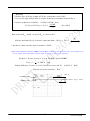
1
AU6803
AU6804
USERS MANUAL
- 1 -
xxxxxxxxxW00
Table of Contents
Safety Precautions ........................................................................................... - 5 1.Introduction ..................................................................................................... - 6 1.1
1.2
1.3
1.4
1.5
Product Overview ......................................................... Product Features.......................................................... Block Diagram ............................................................ Spec Overview ............................................................ Related Documents ........................................................ -
6
6
7
8
8
-
2.Pin List (Name and Functions) .................................................................... - 9 2.1 Pin Assignment ........................................................... - 9 2.2 Pin Description .......................................................... - 10 -
3.Setup Flow .................................................................................................... - 12 4.Peripheral Circuit Design ............................................................................ - 13 4.1 Example of Peripheral Circuit ............................................... 4.2 Analog Interface ......................................................... 4.2.1 Resolver Excitation Circuit ............................................ 4.2.2 Resolver Signal Input Circuit .......................................... 4.2.3 Loop Filter Circuit ................................................... 4.2.4 Analog velocity Output ............................................... 4.3 Digital Interface .......................................................... 4.3.1 Mode Setting・Function Selection ....................................... 4.3.2 Output Interface .................................................... 4.3.3 Clock for Excitation .................................................. 4.4 Power Source ........................................................... 4.5 Countermeasures for Noise ................................................ -
13
14
14
21
24
25
26
26
29
35
35
36
-
5.Connection .................................................................................................... - 37 5.1 Example of Resolver Connection ............................................ - 37 5.2 Example of Power Connection .............................................. - 39 -
6.Check Point of Operation ........................................................................... - 40 6.1 Check Point for Resolver Interface .......................................... 6.1.1 Check Point of Excitation Signal .................................... 6.1.2 Check Point of Monitor Signal Amplitude ................................. 6.1.3 Check Point of Phase Shift............................................ 6.2 Check Point for Digital Output .............................................. 6.2.1 Check Point of Output Angle .......................................... 6.2.2 Check point of abnormality Detection ................................... -
40
40
40
41
44
44
44
-
7.Built In Self Test(BIST)Function ............................................................. - 45 7.1 Run-Time Behavor of BIST................................................. - 45 7.2 Execution Method of BIST ................................................. - 46 -
- 2 -
xxxxxxxxxW00
7.3 Result of BIST ........................................................... - 48 -
8.Function of Fault Detection ....................................................................... - 49 8.1 Abnormal Resolver Signal(Square-sum method)................................ 8.1.1 Concept Detection................................................... 8.1.2 Circuit Configuration ................................................. 8.1.3 Detection Principle .................................................. 8.1.4 Relationship of threshold and Typical abnormal detection pattern............. 8.2 Break Detection of Resolver Signal Line(DC-bias method) ....................... 8.2.1 Concept Detection................................................... 8.2.2 Circuit Configuration ................................................. 8.2.3 Detection Principl ................................................... 8.2.4 Relationship of threshold and Typical abnormal detection pattern............. 8.3 Abnormal R/D conversion(PLL Unlock) ...................................... 8.3.1 Concept Detection................................................... 8.3.2 Circuit Configuration ................................................. 8.3.3 Detection Principl ................................................... 8.3.4 Relationship of threshold and Typical abnormal detection pattern............. 8.4 Abnormal High Temperature inside IC ........................................ 8.4.1 Concept Detection................................................... 8.4.2 Circuit Configuration ................................................. 8.4.3 Detection Principl ................................................... 8.4.4 Relationship of threshold and Typical abnormal detection pattern............. 8.5 Fault Detection Contents and Error Code ..................................... 8.6 Error Reset ............................................................. -
49
49
49
50
50
51
51
52
52
52
53
53
53
53
54
54
54
54
55
55
55
56
-
9.If you think trouble shooting..................................................................... - 57 9.1 In case of error detection .................................................. 9.1.1 Suspicion of Abnormal Resolver Signal (Square-sum method) ................ 9.1.2 Suspicion of Break Detection (DC-bias method) ........................... 9.1.3 Suspicion of Abnormal R/D conversion (PLL Unlock) ....................... 9.2 In case of wrong angle data ................................................ 9.2.1 In case of fixed angle data ............................................ 9.2.2 In case of indefinite, free run, can not get one-rotation data ................ 9.2.3 In case of rotation direction difference, 90°deviation or 180°deviation ....... 9.2.4 In case of rapid change in the output angle data and disturbance ............. 9.3 If the situation does not improve ............................................ -
57
58
60
61
62
63
64
65
66
66
-
10.Electrical characteristics ......................................................................... - 67 10.1
10.2
10.3
10.4
10.5
10.6
10.7
10.8
10.9
Absolute maximum rating.................................................. Power-related characteristic .............................................. R/D conversion characteristic ........................................... Built-In Self-Test(BIST) characteristic .................................... Failure detection characteristic ............................................ Analog signal characteristic ............................................... DC characteristics of digital signal .......................................... AC characteristics of digital signal .......................................... Timing diagram .......................................................... -
67
67
68
68
69
70
71
71
72
-
11.Appendix ...................................................................................................... - 75 - 3 -
xxxxxxxxxW00
11.1 R/D conversion principle .................................................. 11.2 About the error of resolver system ......................................... 11.2.1 Error sources ...................................................... 11.2.2 Error estimates .................................................... 11.3 FAQ................................................................... 11.4 Terms and Definitions .................................................... -
75
77
77
78
79
93
-
12.Revision history.......................................................................................... - 95 -
- 4 -
xxxxxxxxxW00
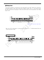
Safety Precautions
Caution!
Before use smartcoder, please carefully read the specification
and this manual for proper use. Incorrect usage do not operate
normally, may damage the equipment that is connected to this
product or this product.
Retain this manual, and please re-read when in doubt.
■Notes
Smartcoder (AU6803, AU6804) is an integrated circuit (i.e electronic device) with a high grade
quality level, but the predictable failure rate is not zero. Also there are some possibility to do
unplanned work cause of noise, static electricity, wiring error, etc. The user is advised, therefore,
that multiple safety means be incorporated in your system or product so as to prevent any
consequential troubles resulting from the failure of our smartcoder (AU6803, AU6804).
These application samples which listed in this manual are reference examples. If you use these
examples, please make sure that you understand your system, equipments, and those functions
and safety.
And the content written in this manual might be changed as needed. For the latest content,
please contact your sales representative.
■Product Warranty
(1)Warranty Period
The warranty period for Smartcoder (AU6803, AU6804) is one year after shipping. Failed
products within this warranty period will be replaced with new one.
(2)Coverage
Even if within the warranty period, we will not take responsibility for the products which show
quality degradation caused by deviant usage against this document or specification like below.
・In case of usage of unguaranteed condition/environment/handling nonlisted in this manual or
specification.
・In case of Remodeling/Repair which is not done by Tamagawa-seiki.
・In case of misusing this product.
・In case of unforeseen matters which can not expect at technology level of shipping age.
- 5 -
xxxxxxxxxW00
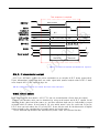
1.Introduction
1.1 Product Overview
Smartcoder(AU6803:For automotive、AU6804:For general use ※ )is an R/D (Resolver to Digital)
conversion IC used with a brushless Resolver (BRX) such as Singlsyn, Smartsyn, etc. It converts
the electrical information (analog signal) corresponding to a mechanical rotational angle of the
Resolver to the corresponding digital data and output it.
It adopted the newly developed Twin-PLL R/D conversion method. And it was developed as
simple usage, low cost, and having high quality, while maintaining high reliability that the Resolver
(Synchro) system has had conventionally. It provides you wide range applications for angle
detection.
※ The difference between AU6803 and AU6804 means excuting burn-in process or not. AU6803 applied
burn-in process. The functions and characteristics are same.
1.2 Product Features
■Real time output
Max tracking rate : 240,000min -1 ( External CLK:10MHz ∼ 12MHz
Max angular acceleration : 1,000,000rad/s 2 .
Operation ) 、
■All-in-one design
Eliminates phase adjustment of exciting signal ( allowable phase angle :±45°
while exciting signal 1 period is 360°). Implemented a Oscillator and a excitation
amplifier (current control type) help to reduce system cost.
■Small・Light weight
7×7mm(Pin pitch: 0.5mm、48pin-LQFP、weight: 0.3g)。 Achieve half package area
against conventional product (AU6802N1).
■Enhance error detection function
Followings are implemented. Abnormal Resolver Signal; Breaking of Resolver Signal
Line; Abnormal R/D conversion; Abnormal High temperature inside IC.
■Implemented BIST(Built-In Self Test)function
R/D conversion function and breaking detection of signal line can be tested
themselves.
■Rich output form
Binary-code Parallel 12bit Bus compatible、Positive logic+ A,B,Z + Serial I/F.
■DC+5V Single Power Supply
- 6 -
xxxxxxxxxW00
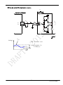
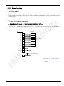
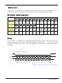
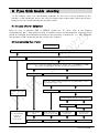
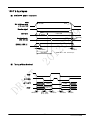
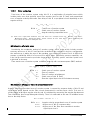
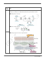
1.3 Block Diagram
VCC
SINMNT
LFUI
LFUO
LFLI
LFLO
VELP
VELN
VDD
Bu f
.
S2
S2
S4
S4
COSMNT
Bu f
(sinθ·sinωt )
VCO
Analog
signal
processing
PSG
Counter
PSG
S1
S1
S3
S3
VCO
(cosθ·sinωt)
Counter
VRR
R1
R2
Digital
signal
processing
Input/
output
interfaces
Serial I/F
Sine wa ve
genera tor
OSC
Self-dia gnosis
( Bu ilt - In Se lf -tes t)
Fa ilu re
detection
S ett in g
r eg is t er
D11
D10
D9
D8
D7
D6
D5
D4
D3
D2
D1
D0
PRT Y
CSB
I NH B ( RD )
A
B
Z
SSCS
SSDT
SCK
SCSB
DATA
RGND
AGND
BISTVLD ERRSTB ERR ERRHLD
CLKIN
- 7 -
DGND
xxxxxxxxxW00
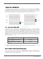
1.4 Spec Overview
Output form
Binary code parallel 12bit bus compatible, Positive logic
+ A, B, Z + Serial I/F
Resolution
4,096 (212)
Conversion accuracy(Static)
±4 LSB
Settling time
(Step input 180°in electric angle)
1.5 ms typ.
180,000 min-1
240,000 min-1
Max. tracking rate
(10MHz<External CLK≦12MHz Operating)
(Internal CLK or 8MHz<External CLK≦10MHz
operating )
Max. angular acceleration
1,000,000 rad / s2
Response (As output response delay
in electric angle)
±0.2°Max./10,000 min-1
Encorder emulation output(A,B)
1,024 C/T
Resolver excitation amplifier
(current control type)
9.5mArms、10kHz typ.
Fault detection function
・Abnormal resolver signal
・Breaking of resolver signal line
・Abnormal R/D conversion
・Abnormal high temperature inside IC
BIST function
(BIST:Built-In Self Test)
・BIST of R/D conversion (Test for R/D conversion)
・BIST of failure detection (Test for broken wire)
Power source
DC 5V±10% 60mA max.
Operating temperature
-40 ∼ +125℃
Storage temperature
-65 ∼ +150℃
Humidity
90% RH max. (No condensation)
Mass
0.3g max.
1.5 Related Documents
(1) SPC007898Y00
(2) SPC008948Y00
Twin-PLL type smartcoder AU6803 Specifications
AU6804 specification (Japanese version)
- 8 -
xxxxxxxxxW00
2.Pin List (Name and Functions)
D0
D1
D2
D3
D4
D5
D6
D7
D8
D9
D10
D11
2.1 Pin Assignment
36
25
VDD 37
INHB(RD)
ERRHLD
ERRSTB
ERR
A
B
24 DGND
SCK
PRTY
SCSB
DATA
SSCS
SSDT
CLKIN
BISTVLD
R1
VRR
13 R2
Z
CSB
LFLO
LFLI
LFUI 48
12
LFUO
VELN
VELP
VCC
SINMNT
COSMNT
AGND
S3
S1
S2
S4
RGND
1
- 9 -
xxxxxxxxxW00
2.2
Pin Description
Pin
No
Symbol
Class
1
LFUO
A /O
E xte rnal filter connect ion te rminal.
Connect rec ommen de d electorical component s to LFUI te rminal.
(4.2.3)
2
VELN
A /O
3
VELP
A /O
Diffe rent ial an alog veloc ity out put s.
The voltage corre spon din g to the ve loc ity out put bet ween VE LP-VELN.
(4.2.4)
4
V CC
――
5
SINMNT
A /O
Re solve r signal(SIN) mon itor out put.
be approximately 2 Vp- p for th is pin.
6
COSMNT
A /O
Re solve r sign al(COS) monitor out put . In put gain sh ould be adjuste d to
be approximately 2 Vp- p for th is pin.
7
AGND
――
8
S3
A /I
9
S1
A /I
10
S2
A /I
11
S4
A /I
12
R GND
――
13
R2
A /O
14
V RR
――
15
R1
A /O
16
BISTVLD
D/I
17
CLKIN
D/I
18
SSDT
D/I
19
SSCS
D/I
DATA
D/ O(BUS)
( Re fe re n c e c h a pte r # )
An alog powe r pin . Connect to +5 V.
(4.4)
In put gain shou ld be adju ste d t o
An alog ground pin. Connect t o 0 V.
Re solve r sign al ( S3 ) in put pin.
settin g resist or of re solve r sign al
Re solve r sign al ( S1 ) in put pin.
settin g resist or of re solve r sign al
Re solve r sign al ( S2 ) in put pin.
settin g resist or of re solve r sign al
Re solve r sign al ( S4 ) in put pin.
settin g resist or of re solve r sign al
This signal ente rs
in put c ircuit.
This signal ente rs
in put c ircuit.
This signal ente rs
in put c ircuit.
This signal ente rs
in put c ircuit.
throu gh the gain
throu gh the gain
throu gh the gain
(4.4)
E xcit in g amplifie r powe r pin. Conne ct to +5V.
SCSB
D/I
22
PR TY
D/ O(BUS)
23
SCK
D/I
24
DGND
――
(4.2.1)
(4.4)
E xcit in g output ( R1 ) pin. Sinu soidal wave form curren t 9.5 mArms(typ)
which can exc ite re solve r directly out put bet ween R1-R2.
BIST function cont rol pin.
BIST function can run when BISTVLD is L level an d se rial settin g
re sistor set for BIST ope ration code.
BIST cont rol
E xcutable
Not excut ion
BISTVLD
L
H
Cloc k in put pin for e xte rnal c loc k mode. In put c loc k fre quency shou ld
be in a ran ge of 10 MHz±20%.
Se rial settin g data in put pin.
While SSCS is “L”, the input SSDT data is synch ronize d t o SCK an d
set to pre- sett ing registe r. The data load to cont rol re giste r at SSCS
ascen din g timin g, then ne w syst em settin g will be made.
Ch ip Select pin for se rial inpu t sett ing function . Th is signal con trol
SSDT dat a rece ption an d rene wal syste m sett ing at ascen ding t iming.
If you do n ot u se se rial in put funct ion, please c onnect t o VDD.
(4.2.1)
(7)
(4.3.3(2))
(4.3.1(2))
Not acce pte d
H
Se rial data out put pin. When SCSB in put falls down, se rial output data
t ran smit with synch ronizat ion to the SCK.
Ch ip Se lect pin for se rial out put funct ion. Th is signal cont rol DATA pin
out put an d latch t ran smitt ing data when SCSB in put falls down.
21
(4.2.2)
throu gh the gain
E xcit in g output ( R2 ) pin. Sinu soidal wave form curren t 9.5 mArms(typ)
which can exc ite re solve r directly out put bet ween R1-R2.
Acce pte d
L
(4.2.2)
(4.4)
E xcit in g amplifie r groun d pin. Connect to 0V.
SSDT Chip Selec t
SSCS
20
Re marks
De sc ript ion
DATA pin ou t
SCSB
Dat a out put
L
Hi Impe dance
H
Even parit y signal pin for out put dat a( D0∼D11). “H” le bel nu mbe r of
D0 ∼D11, PR TY pins must be e ven.
Se rial Cloc k in put pin. Use for serial in put sett ing funct ion an d se rial
out put func tion. Max fre quency is 5 MHz.
Digital groun d pin. Connect t o 0 V.
(Note) “Class” me ans as follo.
* A /I
: Analog in put
* A /O
: Analog out put
(4.3.2(2))
(4.3.1(2),
4.3.2(2) )
(4.4)
* D/I : Digital in put
* D/O(BUS) : Digit al out put(3- state out put)
- 10 -
xxxxxxxxxW00
Pin
No
Symbol
Class
25
D11
D/ O(BUS)
26
D10
27
D 9
28
Re marks
De sc ript ion
Absolute out put mode
( Re fe re n c e c h a pte r # )
Pulse out put mode
φ1 ( MSB)
ER RCD3
D/ O(BUS)
φ2
ER RCD2
D/ O(BUS)
φ3
ER RCD1
D 8
D/ O(BUS)
φ4
ER RHLD
29
D 7
D/ O(BUS)
φ5
ER R
30
D 6
D/ O(BUS)
φ6
−
31
D 5
D/ O(BUS)
φ7
W
32
D 4
D/ O(BUS)
φ8
V
33
D 3
D/ O(BUS)
φ9
U
34
D 2
D/ O(BUS)
φ10
Z
35
D 1
D/ O(BUS)
φ11
B
36
D 0
D/ O(BUS)
φ12 (LSB)
A
37
V DD
――
38
39
INHB(R D)
ER RHLD
D/I
D/O( I)
(4.3.2 (1))
Digital powe r pin. Connect to +5V.
Inhibit (Re ad) pin. Th is signal switchs th rou gh/hold
corre spon din g pin s.
■Absolut e out put mode: φ1∼φ12, PR TY
■Pulse out put mode: U, V, W, ERR, ERR HLD, ERR CD1∼3
(4.4)
for
be low
(4.3.2)
Target out put pin statu s
Th rou gh
Hold
INHB(R D)
H
L
ERR ( Hold) pin . Once an abn ormal con dition is detecte d, this signal
chan ge to H an d kee p this level until e rror re set.
This pin also se rve s as the defau lt out put mode sett ing for D0∼D11. It
is e xcute d by sen sin g the voltage le vel at powe r-u p as an in put pin,
which has a pull-u p re sistor(10 kΩ) or pull- down re sist or(10 kΩ).
D0 ∼D11 de fault settin g
ER RHLD pin t reat ment
Absolute out mode
10 kΩ pull-u p
(8,
4.3.1(1) )
Pulse out mode
10 kΩ pull- down
E rror re set pin . Th is signal rese t ER RHLD an d ERR CD1∼3 .
40
41
ER RSTB
ERR
D/I
D/O( I)
ER RHLD,ERR CD1∼3 statu s
ER RSTB
Hold
H
ER R out put pin. While the e rror is detecte d, out put “H” leve l.
This pin also se rve s as the de fau lt mode sett ing for ope ration cloc k. It
is e xcute d by sen sin g the voltage le vel at powe r-u p as an in put pin,
which has a pull-u p re sistor(10 kΩ) or pull- down re sist or(10 kΩ).
Cloc k de fault settin g
ER R pin t reat ment
Inte rnal oscillat or
10 kΩ pull-u p
42
A
D/O
E quivalen t to an encode r A pu lse out put pin.
43
B
D/O
E quivalen t to an encode r B pu lse out put pin.
44
Z
D/O( I)
(8.6)
Clear (re set)
L
(8,
4.3.1(1) )
E xte rnal c lk in put
10 kΩ pull- down
(4.3.2(3))
E quivalen t to an encode r Z pulse out put pin.
This pin also se rve s as t he defau lt mode settin g for e xcit ation mode. It
is e xcute d by sen sin g the voltage le vel at powe r-u p as an in put pin,
which has a pull-u p re sistor(10 kΩ) or pull- down re sist or(10 kΩ).
Ex c itat ion mode defau lt s etting
Curre n t exc ita tion
Vo ltag e e xc it ation
Z pin t reat ment
10 kΩ pull-u p
10 kΩ pull- down
(4.3.2(3),
4.3.1(1) )
Ch ip selec t(CSB) pin. Th is signal con trols D0 ∼D11, PR TY pin s.
45
CSB
D/I
46
LFLO
A /O
47
LFLI
A /I
48
LFUI
A /I
D0 ∼11, PR TY pin sett ing
CSB
E xte rnal
Connect
E xte rnal
Connect
E xte rnal
Connect
(Note) “Class” me ans as follow.
* A /I
: Analog in put
* A /O
: Analog out put
Dat a out put
L
Hi Impe dance
H
filter connect ion te rminal.
rec ommen de d electorical component s to LFLI te rminal.
filter connect ion te rminal.
rec ommen de d electorical component s to LFLO te rminal.
filter connect ion te rminal.
rec ommen de d electorical component s to LFUO te rminal.
*
*
*
*
(4.3.2(1))
(4.2.3)
(4.2.3)
(4.2.3)
D/ I : Digital in put
D/O : Digital out put
D/O(I) : Digital out put( With inte rnal pull-u p for in put)
D/O(BUS) : Digit al out put(3- state out put)
- 11 -
xxxxxxxxxW00
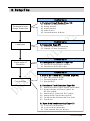
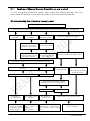
3.Setup Flow
Related topics
4.Peripheral Circuit Design(Page-13)
Peripheral circuit
design/Production
4.1
4.2
4.3
4.4
4.5
Example of Peripheral Circuit
Analog Interface
Digital Interface
Power Source
Countermeasures for Noise
Related topics
Connection
5.Connection(Page-37)
5.1 Example of Resolver Connection
5.2 Example of Power Connection
Related topics
Check point of
Operation
6.Check point of Operation(Page-40)
6.1 Check Point for Resolver interface
6.2 Check point for Digital Output
Related topics
7.Built In Self Test(BIST) Function(Page-45)
Practical use
7.1 Run-Time behavior of BIST
7.2 Execution Method of BIST
7.3 Result of BIST
8.Function of Fault Detection(Page-49)
8.1 Abnormal Resolver Signal (Square-sum method)
8.2 Break Detection of Resolver Signal Line
(DC-bias method)
8.3 Abnormal R/D conversion (PLL Unlock)
8.4 Abnormal High Temperature inside IC
8.5 Fault Detection Contents and Error Code
8.6 Error Reset
9.If you think troubleshooting(Page-57)
9.1 In case of error detection
9.2 In case of wrong angle data
9.3 If the situation does not improve
- 12 -
xxxxxxxxxW00
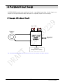
4.Peripheral Circuit Design
AU6803/AU6804 require some peripheral circuit to get digital angle data. In this chapter, we
explain the design method and important point for required peripheral circuit design.
4.1 Example of Peripheral Circuit
Loop Filter
Resolver
(BRX)
AU6803
(AU6804)
Digital I/O
Angle data
DC+5V
(Single power supply)
※ Some applications will require an external clock input and separate excitation amplifier.
- 13 -
xxxxxxxxxW00
4.2 Analog Interface
※ Examples mentioned in this articles shows only the concept of basic functions. Please note that each
application might have their each individual requirement. Therefore the circuit configulation and the decision
of constants for practical resistors and the function of protection for input/output circuits, etc. should be
designed for each application by customer.
4.2.1
Resolver Excitation Circuit
(1)Direct Excitation
AU6803(AU6804) has an excitation amplifier in the IC then it is possible to excite resolver
directly. It is constant-current amplifier and its current value is 9.5mArms(typ). In case you do
not put separate amplifier, it is ideal for cost-sensitive application usage.
Note that the lower the input impedance value shows lower exciting voltage then it need noise
considerations. In such case, exciting voltage booster amplifier can be placed separately as
shown in the following section.
AU6803(AU6804)
9.5mA rms. (typ.)
R1
R1
15
Resolver
Input Impedance:Zro [Ω]
RS
R2
13
R2
For specific circuit configuration,
please refer to P37.
R1-GND
R2-GND
2.1V DC (typ.)
Voltage
(Zro×0.0095×√2)Vp-p
Time
Voltage
R1-R2
Time
- 14 -
(Zro×0.0095×√2×2 )Vp-p
【Ex】 Zro=120Ω then
3.21Vp-p
xxxxxxxxxW00
(2)Separate excitation amplifier
In case of severe noise environments, exciting voltage booster amplifier can be placed
separately. There are 2 type of excitation amplifier circuit, current control type and voltage
control type. Show merit/demerit of each method below. Please determine appropriate method
for your system considering them.
Excitation Amp.
Merit
Demerit
Current
control ・ Prevention of secondary ・ Circuit is getting complex,
type
failure(damage of output TR. and it might not operate as
Etc.) by short circuit between caliculations.
exciting lines.
・ Exciting voltage might vary
・ Resolver output fluctuations due
to
resolver
input
caused temperature change impedance variability.
can be suppressed by a
constant excitation current.
Voltage
type
control
・ Circuit is simple and it will ・Possibility to have secondary
operate as caliculations.
failure due to overcurrent in
case
of
short
circuit
・ Exciting voltage can be
between exciting lines.
constant.
・ Easier to get the resolver
output
variation
due
to
temperature changes.
Separate power supply (V E XT ) is required for the excitation amplifier circuit, in addition to the
AU6803(AU6804) +5V power supply.
Higher resolver exciting voltage caused higher resolver output voltage and it can expect to
improve the S/N ratio or noise immunity. That mean it need appropriate DC power supply. For
example, exciting voltage 7Vrms ( = 20Vp-p : 7V × √ 2 × 2 ) require + 24V for single power
source or ±15V for dual power sources.
Resolver operation will be possible at the lower exciting voltage compared to the value
described in the specification. So please decide exciting voltage value considering noise immunity
and power equipment which can be prepared.
In this chapter, we will show you the example of excitation amplifier circuit (current control
type) using AU6803(AU6804) exciting output(R1,R2).
- 15 -
xxxxxxxxxW00
■Example circuit for single power source
AU6803(AU6804)
Rf
+ VEXT
Q1
V RS O
R1
15
R2
13
Ci
+ VEXT
R
Ri
Ri
Q2
10 kΩ
R IE X T
Rf
10 kΩ
R2
Rf
R1
+ VEXT
R IE X T
Q3
Ri
V RS O
Ci
Ri
Q4
Rf
Cf
DC cut capacitor
Voltage
V RS O
Emitter resistance
Bias circuit
Current
sensing
resistor
V RS O
【Ex】 R=150Ω case
150×0.0095×√2
=2.00Vp-p
Time
In case of V EXT variation is expected by battery power, it
must be defined standard operating at minimum voltage.
- 16 -
xxxxxxxxxW00
■Example circuit for dual power source
Cf
AU6803(AU6804)
Rf
+ VEXT
Q1
V RS O
R1
15
R2
13
Ci
Ri
R
Ri
Q2
R IE X T
- VEXT
R2
Rf
R1
V RS O
Voltage
【Ex】 R=150Ω case
150×0.0095×√2
=2.00Vp-p
Time
- 17 -
xxxxxxxxxW00
■Method for Setting constants of separate excitation amplifier(sample)
Refer below for setting constants.
≪Description
+V EXT ,−V EXT :
I REF :
R IEXT :
V RE F :
Z RO :
V RSO :
of symbol≫
External power supply(For exciting voltage booster amplifier circuit)
Exciting current of Resolver
Resistor for setting exciting current of Resolver
Exciting voltage of Resolver
Input impedance of Resolver(Specified value)
R1(or R2) pin output voltage
Step① : Calculate the exciting current by setting the exciting voltage based on
the voltage of external power supply.
V RE F = I REF × Z RO
Step② : Calculate the circuit constants based on the exciting current.
I RE F /2 =( V RSO ×Rf )/( R IEXT ×Ri ) ・・・・・For single power source
I REF
=( V RS O ×Rf )/( R IEXT ×Ri ) ・・・・・For dual power source
< Setting condition>
・ R IEX T ≦(Z RO /10) [Ω]
・ Rf≧50kΩ ,Ci×Ri≧5×10 −4 [s] ,Cf×Rf≦5×10 −6 [s]
・ The power supply for an operational amplifier should be the same as
that for the transistor buffer.
※This calculation method is based on DC circuit concept.
Resolver is a AC circuit and that input impedance (= R (RE SISTANCE) +jX (CONDUCTOR) ) cause
voltage phase shift and current phase shift. Also there are some impacts at parallel
connection of Rf and Cf. Then it might not get exact exciting voltage value as calculated.
In such a case, please adjust each constant by yourself. (Voltage can be adjusted by Ri value)
And it is effective to make pre-validation using circuit simulation like SPICE.
- 18 -
xxxxxxxxxW00
【Example】
V EX T =Battery 12V(8V∼16V fluctuation), Excitation frequency=10KHz,
Resolver Spec [ Input impedance=76Ω (R-part:18Ω+L-part:1.18mH)]
Let s excite this resolver with current type amplifier described in P16.
V EX T define as 8V(use minimum fluctuation).
Saturation voltage of OP-AMP assume as x0.8 supply.
8V×0.8=6.4V
Regarding R1-GND and R2-GND,
Set amplitude center as 4V DC (=8V×1/2).
Set amplitude as 4Vp-p.
Then target amplitude is set as R1-R2=8Vp-p .
Voltage
R2−GND
R1−GND
Max: under 6.4V
4VDC center (=8V×1/2)
Time
According to the formula of P18,
Resolver excitation current(I R EF )=0.11Ap-p (=8Vp-p/76Ω)
R IE XT =4.7Ω < Resolver input impedance(76Ω)/10
Rf=100kΩ
Then,
I R EF =
Ri=
VRSO Rf
・・・・・For single power source
R IEXT Ri
VRSO Rf
R IEXT I REF 1 / 2
=774kΩ
2Vp - p 100k
4.7 0.11 1 / 2
=
<---->
(Please adjust at actual circuit.)
Example of circuit simulation,
Resolver input impedance
=18Ω+1.18mH
Cf
=100p
Emitter resistance =4.7Ω
Bias resistance=1kΩ
Then around Ri = 460k Ω . (8Vp-p
between R1-R2)
- 19 -
xxxxxxxxxW00
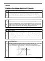
【Single power source V E XT =12V waveform sample】
−Normal operation case−
R2-GND
7Vp-p
R1-GND
6V center (=1/2・V EXT )
14Vp-p
0V center
R1-R2
−Trouble(distortion) case−
R2-GND
The wrong constant selection cause
wider amplitude, and waveform
distortion will be occurred by OP-AMP
or Tr saturation voltage, etc.
Need to avoid distortion.
R1-GND
Rail to Rail OP-AMP type
(saturation voltage is close to
supply voltage) can set wider
active output voltage without
distortion generation.
R1-R2
R1-GND
It might happen to have
R1-GND/R2-GND oscilation due
to OP-AMP characteristic.
If this kind of wave is observed,
DC cut Capacitor (Ci) might
cause unstability of DC current.
Then insersion of resistor
between Ci output and GND will
be effective to stabilize it.
R2-GND
Ci
Ri
R1-R2
Addition al re sist or
(around 100 kΩ)
- 20 -
xxxxxxxxxW00
4.2.2
Resolver Signal Input Circuit
R/D conversion of AU6803(AU6804)will be done with monitor output( SINMNT, COSMNT).
While voltage level of resolver signal is different with each application, it need to set
appropriate monitor signal level with gain adjustment of resolver input signal to fit R/D
conversion effectively. Also it need to have external DC bias resistor activating the function
which detect any breaking of Resolver signal lines (S1~S4) mounted in AU6803(AU6804).
In this chapter, show you example of resolver signal input circuit.
■Example of resolver signal input circuit
AU6803(AU6804)
V CO M
( =2.25V)
+ VCC
Mon itor out put
COSMNT
(SINMNT)
Resolver signal level
6 (5)
40 kΩ
RH
S1 (S2 )
40 kΩ
R IN /2
R IN /2
S1
180 Ω
RF
180 Ω
RF
9 (10)
(S2)
CN
S3
R IN /2
R IN /2
S3 (S4 )
CC
CC
8 (11)
(S4)
RL
R F =41.5 kΩ±9%
(1,000 pF×2 )
Common-mode
capacitor
DC bias resistor to
detect breaking
Gain setting resistor
Normal-mode
capacitor
(1)Gain setting resistor
The relationship between input resolver signal amplitude and monitor amplitude shows below.
Monitor amplitude[Vp-p]=Resolver signal amplitude [Vp-p]×(1/2)×
RF
RIN
Gain setting resistor (R IN ) is defined as monitor MAX amplitude 2Vp-p .
- 21 -
xxxxxxxxxW00
【Example】
Resolver spec (Exciting voltage: AC7Vrms, transformer ratio: 0.286),
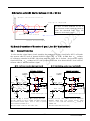
Use it as exciting voltage 10Vp-p, monitor output max amplitude assumed 2Vp-p.
Resolver output max=2.86Vp-p (=10Vp-p×0.286) then,
2.0 Vp-p=2.86 Vp-p×(1/2)×
41.5k
R IN
∴R IN =30kΩ
Note, assumed R IN ≧2kΩ. In case of R I N is close to 2kΩ,
Monitor amplitude[Vp-p]=Resolver signal amplitude [Vp-p]×(1/2)×
RF
R I N 180Ω
Like above, please consider input resistance (=180Ω) .
※If potential difference between SINMNT and COSMNT generate by the deviation of R I N , it will caused error
source. Please select appropriate resistor grade according to your system tolerance.
[Example] In case of there is a +Δ COSMNT against SINMNT,
Error =−
1
・Δ・SIN2θ [rad]
2
(Voltage difference 1% case: Δ=0.01 Then Error max.=±0.29°(=±0.01/2 [rad])
Example of monitor waveform (At 0°)
2Vp-p
COSMNT-GND
2.25V D C (typ.) center
SINMNT-GND
- 22 -
xxxxxxxxxW00
(2)DC bias resistor to detect breaking (R H 、R L )
When the signal line come down, monitor output level must be exceeded the threshold value and
it need to set appropriate resistance value.
(1) R H ≒{(4.5−V C OM )/(12.5×10 -6 )}- R I N
(2) R L ≒{V C OM /(12.5×10 -6 )}- R I N
While
V C OM =2.25[V]
Resistor value is determined in the range of 80~100% of the caliculated value.
In general,
R H ,R L =(180kΩ−R IN )×(0.8∼1.0)
Without this DC bias resistor, fault detection depend on its angle (Could be detect at
somewhere in rotation).
(Without this DC bias resistor, monitor output signal of breaking line will be about 0Vp-p. So
when the normal monitor output signal rotate to the position which is detected as fault range,
abnormality is detected by the square sum method. )
(3)Normal mode capacitor (C N )
While basic circuit doesn t have C N , it can improve electorical noise.
But the gain resistor(R I N ) and C N work as filter, it cause one of factor of phase shift.
Time constant=2×((R I N /2)//(R I N /2))×C N
※ (R I N /2)//(R I N /2)means parallel connection resistance value of (R I N /2) and (R I N /2).
This capacitor has an impedance{=1/(ω・C N )} and it affect signal level also.
Deviation of capacitor is much worse than that of resistor, please select the small deviation
parts or small capacitance part to avoid impact of signal level.
(4)Common mode capacitor (C C )
Standard usage is putting 1000p capacitor between S1~S4 signal and GND.
- 23 -
xxxxxxxxxW00
4.2.3
Loop Filter Circuit
In this product, loop filter circuit is one of the factors configuring the negative feedback control
system to perform R/D conversion. To operate R/D conversion successfully, the electonic
parts shown in below figure should be connected between LFUI and LFUO terminals, and
LFLI and LFLO terminals respectively.
■Connection configuration of loop filter
∼
AU6803(AU6804)
LFUI( LFLI)
48(47)
22 kΩ
0.0022 μF
0.022 μF
1(46)
∼
LFUO(LFLO)
Regarding loop filter connection, please connect wiring compact as much as possible with
given the constant of resistor and capacitor. Especially input terminals (LFLI, LFUI) must be
carefull not to enter noise due to sensitive terminals.
Also please select appropriate parts (especially capacitor) which meet required characteristic
for temperature range.
- 24 -
xxxxxxxxxW00
4.2.4
Analog velocity Output
■Considerations in analog velocity output
AU6803 (AU6804) has an analog velocity output terminal. But its accuracy is a rough so we do
not recommend it for control.
Example of configuration register setting Bit11=1 , (VELP−VELN)=100(typ.) [μV/min -1 ],
then ±10,000min -1 means ideally ±1V( typ.) output. But we can not get an accurate
output cause of voltage offset [ = ± 2V ( max. ) ] and gain error [ = -30 % / + 20 % ] and
temperature coefficient.
■How to use
The following is an example of the speed voltage output.
example:gain=1
AU6803
(AU6804)
20kΩ
20kΩ
VELN
2
-
VELP
3
+
VELP-VELN
20kΩ
20kΩ
COM
Setting register
Bit11=0 case
voltage
VELP-VELN
voltage
COM+1V
VELN-GND
2.25V+0.5V
2.25V(typ.)
2.25V−0.5V
COM
COM−1V
VELP-GND
-10
Setting register
Bit11=1 case
0
10
velocity
[×100,000min -1]
voltage
-10
0
10
velocity
[×100,000min-1]
voltage
COM+1V
2.25V+0.5V
2.25V(typ.)
2.25V−0.5V
-1
0
1
velocity
[×10,000min-1]
COM
COM−1V
-1
0
1
velocity
[×10,000min-1]
(Record) Velocity_Out+Direction=Digital_Out UP Direction
- 25 -
xxxxxxxxxW00
4.3 Digital Interface
4.3.1
Mode Setting・Function Selection
(1)Default setting
AU6803 ( AU6804 ) has a mode-setting function(for below 3-pins) that detects the terminal
voltage level as an input terminal at power-on, by means of adding a pull-up register of 10KΩ or
a pull-down register of 10KΩ to the output terminals.
Please make the appropriate settings for each application in this function.
AU6803(AU6804)
VDD
■Output-mode setting
Output mode
(D0−D11)
Pull-up(10kΩ)
Absolute parallel
angle data
Pull-down(10kΩ)
Pulses equivalent
to encoder
Parallel out pins(D0−D11) mode setting.
Refer section 2.2、4.3.2(1) for actual description.
(Serial output is not covered by this setting.)
※This setting can be rewritten in the serial input configuration.
(Target setting register: Bit 1)
Pull-u p
re giste r
39
ERRHLD
Pull- down
re giste r
DGND
VDD
■Oscillator selection for excitation
Oscillator
Pull-up(10kΩ)
Internal oscillator
Pull-down(10kΩ)
External clk input
Select the source of excitation output.
Internal oscillator: The IC s internal oscillator is used.
External clk:
Use an external clock input.
41
ERR
19
Z
DGND
Excitation frequency= Clk_frequency/1024
※This setting can be rewritten in the serial input configuration.
(Target setting register: Bit 2)
VDD
■Excitaion output mode setting
Excitation
mode
Pull-up(10kΩ)
Current excitation
mode (VMD=0)
Pull-down(10kΩ)
Voltage excitation
mode (VMD=1)
Reference waveform(Current waveform between R1-R2),
and Resolver signal input(SINMNT, COSMNT pin waveform),
Select appropriate mode by checking phase difference of above. DGND
■Phase difference=+90°±45° ■Phase difference= 0°±45° -
Current excitation mode(VMD= 0 )
Voltage excitation mode(VMD= 1 )
※If this mode setting is incorrect, digital output angle value will shift 180 degree.
※This setting can NOT be rewritten in the serial input configuration.
- 26 -
xxxxxxxxxW00
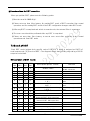
(2)Serial input setting
AU6803(AU6804) has a function that makes it possible to change the contents of the setting
register shown in below table through the serial input. At this function, it is possible to set right
operation mode for individual applications, and set the content in diagnostic of BIST function.
※The SSCS input terminal should be connected to the power supply(VDD) when this function is not used.
■Description of serial input setting register
Bit NO.
1
2
3
4
5
6
Items
[0]
[1]
[0]
[1]
:
:
:
:
Setting of serial
output mode
[Bit 4,3]
[00]
[01]
[10]
[11]
:
:
:
:
Signal setting of
Pin No.44
& Pin No.22
[Bit 6,5]
[00]
Se ttin g of out put mode
(D0∼D11)
Selection of
operating clock
7
8
9
Setting of built-in
self-test
(BIST)
operation
[Bit 10,9,8,7]
11
Setting of VEL
output range
(Analog velocity)
12
(Ze ro point pulse out put)
( Parity out put)
[01]
Test output 1
Test output4
[10]
Test output 2
Test output5
[11]
Test output 3
Test output6
[0000]
[0001]
[0101]
[0110]
[0111]
[1000]
[1001]
[1010]
[1011]
[1100]
[1101]
[1110]
10
Setting of threshold
value for abnormal
square-sum
Description of Setting
Absolute value(φ1∼φ12)of parallel angle data.
Pulses equivalent to Encoder(A,B,Z,U,V,W)
Internal oscillator
External clock input
Absolute value(φ1∼φ12)of angle data
Pulses equivalent to Encoder(A,B,Z,U,V,W)
Serial call-back(For checking the setting register)
Result of failure detection/BIST
Pin No.44
Pin No.22
Z output
PRTY output
Ple ase u se the
default value for
Bit5 、6 .
: BISTVLD(Input) invalid
∼ [0100] : Reserved(Do not select this code.)
: BIST of R/D conversion:Command angle 1(0°)
: BIST of R/D conversion:Command angle 2(45°)
: BIST of R/D conversion:Command angle3(270°)
: Reserved(Do not select this code.)
: Reserved(Do not select this code.)
: BIST of failure detection:BIST of breaking of wire
detection for COS signal line.
: BIST of failure detection:BIST of breaking of wire
detection for SIN signal line.
: Reserved(Do not select this code.)
: System Reset
∼ [1111] : Reserved(Do not select this code.)
[0] : 10 μV/min - 1 (0 ∼ 240,000min - 1 )
[1] : 100 μV/min - 1 (0 ∼ 24,000min - 1 )
[0] : 0.7 Vp-p
[1] : 1.0 Vp-p
※ The default value setting is zero (0) for all bits except the specification of 4.3.1(1).
- 27 -
xxxxxxxxxW00
■Setting method
Serial input operation is controlled by SSCS/SCK/SSDT pins. SSDT data will be entered by
synchronized timing to SCK input at the active condition of SSCS input L level. Please switch
the SSDT input at the rising edge of SCK, while SSDT data will be incorporated at the falling
edge of SCK.
Update sett ing re giste r
▼
SSCS
SCK
SSDT
BIT1
(LSB)
SCK=12 CLK
BIT12
(MSB)
※Refer 10.9 to check each signal timing.
Note, when SCK clock number is greater than 12 while SSCS= L , effective data will be last
12 one of the last 12 SCK.
SCK cloc k 12 or highe r
SSCS
SCK
SSDT
BIT1
(LSB)
E ffect ive data is th is ran ge
- 28 -
BIT12
( MSB)
SCK=12 CLK .
xxxxxxxxxW00
4.3.2
Output Interface
(1)Parallel output
Examples of parallel output are as follows. Note that it assumed to make parallel output mode
setting by default setting (refer 4.3.1(1)) in this chapter. It is also OK to use serial input setting
(refer 4.3.2(2)).
■ Usage of Absolute output mode
―《stand-alone》 usage : Interfaced by dedicated I/O―
When it use in standalone, CSB pin must be L lebel. And please read φ1~φ12 data which
control through/hold by INHB(RD) pin.
AU6803(AU6804)
Output data
D11
25
φ1
D10
26
φ2
D9
27
φ3
D8
28
φ4
D7
29
φ5
D6
30
φ6
D5
31
φ7
D4
32
φ8
D3
33
φ9
D2
34
φ10
D1
35
φ11
D0
36
φ12
PRTY
22
CSB
45
INHB(RD)
38
ERRHLD
39
Parallel output
Parity output
Inhibit input [ “L”:fixed data ]
10kΩ pull-up (Absolute mode)
※ Please refer chapter 10.9 for
φ 1 ∼ φ 12 、 PRTY 、 CSB 、 INHB
timings.
- 29 -
xxxxxxxxxW00
―《Bus interface》 usage : Interfaced by BUS line―
When it use in bus line, D0∼D11 and PRTY output state must be controlled by CSB pin. And
please read φ1~φ12 data which control through/hold by INHB(RD) pin.
AU6803(AU6804)
D11
25
D10
26
D9
27
D8
28
D7
29
D6
30
D5
31
D4
32
D3
33
D2
34
D1
35
D0
36
PRTY
22
CSB
45
INHB(RD)
38
φ12
φ1
Data bus
Chip select(CS)
Read(RD)
VDD
10kΩ pull-up (Absolute mode)
ERRHLD
39
※ Please refer chapter 10.9 for
φ 1 ∼ φ 12 、 PRTY 、 CSB 、 INHB
timings.
■Usage of Pulse output mode
When it use in pulse output mode equivalent to an encoder, Set CSB= L and INHB(RD)= H .
AU6803(AU6804)
Output data
D11
25
ERRCD3
D10
26
ERRCD2
D9
27
ERRCD1
D8
28
ERRHLD
D7
29
ERR
D6
30
−
D5
31
W
D4
32
V
D3
33
U
D2
34
Z
D1
35
B
D0
36
A
CSB
45
INHB(RD)
38
ERRHLD
39
VDD
DGND
10kΩ pull-down (Pulse output mode)
※ A,B,Z pulse which come from
D0~D2 pins are same signal with
dedicated A,B,Z pin (42~44 pin).
DGND
- 30 -
xxxxxxxxxW00
―Pulse output equivalent to an encoder―
The waveform of pulse output is shown below.
T
T
T=
N=
A
360 °/ N
1024(12 Bit s)
B
+θ(increase)
‐θ(decrease)
Z
φ1∼φ12
[FFE ]
[FFF]
[000]
1LSB(max.)
[001]
[002]
1LSB(max.)
U
V
W
E lect rical an gle : 0°
(
60°× 6
)
360 °
※The pulses output equivalent to an encoder have a 1-bit hysteresis circuit to prevent chattering. Then
there might have deviation against absolute angle data according to resolver rotation direction.
- 31 -
xxxxxxxxxW00
(2)Serial output
This IC has a serial output data selection function that is defined by mode setting (Bit4, 3) of
serial input setting register. Each serial output mode setting shows below output signals.
■Description of serial output signal
Serial output
mode setting
[Bit 4,3]
1
Setting [00]:
Absolute
output mode
LSB
Setting [01]:
Pulse output
mode
Setting [10]:
Serial
call-back
Setting [11]:
Results of
BIST
2
φ12
3
Bit No. of DATA
5
6
7
4
output
8
9
10
11
12
MSB
φ11
φ10
φ9
φ8
φ7
φ6
φ5
φ4
φ3
φ2
φ1
-
ERR
ERR
HLD
ERR
CD1
ERR
CD2
ERR
CD3
Pulses equivalent to Encoder
A
B
Z
U
V
W
Setting
Setting
Setting
Setting
Setting
Setting
Setting
Setting
Setting
Setting
Setting
Setting
Bit 1
Bit 2
Bit 3
Bit 4
Bit 5
Bit 6
Bit 7
Bit 8
Bit 9
Bit10
Bit11
Bit12
Default Default BIST
Bit 1
Bit 2
CD1
BIST
CD2
BIST
CD3
BIST
CD4
During
BIST
VMD
ERR
HLD
ERR
CD1
ERR
CD2
ERR
CD3
operation
■Usage
Serial output is controlled by SCSB/SCK pins. Serial data output from DATA pin with
synchronized timing to SCK input at the active condition of SCSB input L lebel. DATA output
switch at the falling edge of SCK, so please read output serial data at the rizing edge of SCK
essentially.
The data at t his t ime is t ran smitte d in se rial.
SCSB
SCK
DATA
Bit1
Bit2
Bit3
Bit4
Bit5
Bit6
Bit7
Bit8
Bit9
Bit10 Bit11 Bit12
PR TY
Dat a out put time (12 Bit s + PR TY)
※Please refer chapter 10.9 for each signal timing.
- 32 -
xxxxxxxxxW00
Note, PRTY is defined as even parity. The number of
must be even.
1
data between serial data
Bit1~12
and
PRTY
E xample
SCSB
SCK
DATA
1
0
1
0
1
0
Bit1 ∼12, t he nu mbe r of
Also while SCSB= L
1
0
1
1
0
1
1
1
The nu mbe r of 1 dat a must
be e ven. Then PR TY=1
dat a is 7.
fix and SCK clock keep to enter, 14 th SCK data and beyond shows PRTY data.
More than 14 sc k c ase.
SCSB
SCK
DATA
Bit1 Bit2 Bit3 Bit3 Bit4 Bit5 Bit6 Bit7 Bit8 Bit9 Bit10 Bit11 Bit12
MSB
SCK=13CLK
PR TY
14 th
SCK
PR TY
data
an d
beyon d
kee p
data.
■Considerations for using the serial output
When using the serial output feature, please note the following points.
① In serial output, required time to transmit all bits may generate some dead time in the
control system. Especially it is possible to recognize the present position with some error
in case of using the pulse output equivalent to an encoder.
② The effected signals by INHB are absolute outputφ1∼φ12, PRTY, pulse output equivalent
to encoder U, V, W, and ERR, ERRHLD, ERRCD1∼3 .
③ In case of changing from the serial output mode(except absolute output mode) to absolute
output mode like described below, please follow next page sequence.
【Pulse output mode】
Bit[4,3]=[0,1]
【Serial call-back】
Bit[4,3]=[1,0]
【Results of BIST】
Bit[4,3]=[1,1]
【Absolute output mode】
Bit[4,3]=[0,0]
- 33 -
xxxxxxxxxW00
This sequence is required.
BISTVLD
BIST enabled
SSCS
Contents of
setting register
[Bit No.3∼4]
Except[00]
BIST setting
[Bit No.7∼10]
[0000]
SIN or COS broken wire BIST
Normal operation
Indefinite
D0∼D11
[00]
[0000]
Normal operation
SCSB
Serial output
Absolute mode
Other mode
10ms(min)
10ms(min)
※Above contents corresponds specification P6 figure3-1.
(3)A, B, Z independent pin output
A/B/Z pin (42~44pin) output the pulses equivalent to an encoder A/B/Z phase respectively.
These independent output terminals are same signal with parallel output mode D0~D2. Please
refer chapter 4.3.2(1) for signal timings, etc.
※A/B/Z independent outputs are outside the scope of the CSB input.
(4)Use verbose output
Each output signals described in 4.3.2(1)~(3) can use a combination of more than one signal.
Example the absolute value can be detected by using serial output and A/B/Z signals. Serial
(absolute mode) data load after power on, and then absolute data can be caliculated by count
up/down with A/B phase. It need total 6 I/O pins which mean 3 pins for serial and 3 pins for
A/B/Z then you can reduce the I/O of the CPU. It can also be used for fault detection of digital
output system by the combination of parallel output and serial output.
To suit individual applications and requirement, please utilize this verbose function.
- 34 -
xxxxxxxxxW00
4.3.3
Clock for Excitation
There is an clk selection mode described in 4.3.1(1)default setting or 4.3.1(2) serial setting.
An excitation clk can be generated from internal oscillator or external clock.
(1)Selection of internal oscillator
Using the IC s internal oscillator, then it does not need external clock. CLKIN:17pin (external
clock) should be open.
(2)Selection of external clock
This is useful to set the desired frequency of the excitation frequency. External clock should be
input to CLKIN:17pin. This is TTL-level pin.
Excitation frequency=(External clock frequency)/1024
※ An external clock can be getting to be noise source. Then its board pattern must be as short as possible
with guard GND pattern in order to make effective EMC measures.
4.4 Power Source
∼
AU6803 (AU6804)
VRR
4
VCC
37
VDD
12
R GND
7
AGND
24
DGND
∼
DC+5 V
14
+
100 μF
0.1 μF 0.1 μF
0.1 μF
∼
0V
∼
Power source is single supply +5V±5%. Analog power lines(VCC/AGND), digital power lines
(VDD/DGND) and excitation power lines(VRR/RGND) must connect to each of the same one.
If you set separate power line for VCC-VDD−VRR or AGND-DGND−RGND, there must be no
potential difference and power switching(On/Off) should be done simultaneously.
Above figure is example of power connection. Regarding 0.1uF capacitors, it should be located
close to AU6803(AU6804) device as much as possible.
- 35 -
xxxxxxxxxW00
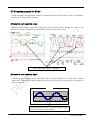
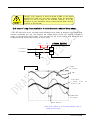
4.5 Countermeasures for Noise
Below waveforms are measured actually. Countermeasure for noise must be done in accordance
with the specification P28 contents.
■Waveforms of magnetic noise
Magnetic noise happens when the leakage flux of the motor passes through the resolver. Its
effect will be bigger turbulence of digital output, which will generate error.
SINMNT
COSMNT
SINMNT
COSMNT
Basic waveform(10kHz) deformed.
■Waveforms of electrical noise
Electrical noise happens when the spike noise caused by PWM drive of the motor affects
signal lines. Turbulence of digital output will not be so big but it will generate error depend on
the size of noise.
サーボオン
3.5
3
2.5
2
1.5
1
501
1001
1501
Basic waveform(10kHz) was not changed much.
But spike noise was overlapped.
- 36 -
xxxxxxxxxW00
5.Connection
Caution!
Please take off the power during connection operation. After
power off, take enough time, check the voltage value by
tester, and please operate wiring and connecting.
5.1 Example of Resolver Connection
■Connenction and configuration example using direct excitation functions of this product.
RH
S1
9
S1
8
S3
10
S2
11
S4
∼
∼
S3
∼
∼
S1
∼
AU6803(AU6804)
VCC
Resolver
(BRX)
S3
CC
CC
RL
AGND
VCC
S4
∼
∼
R1
RH
S2
∼
∼
S4
∼
∼
S2
CC
CC
RL
AGND
(Resolver input impedance + resistance) must be 200Ωor less.
R1
R1
13
R2
44
Z
∼
∼
15
R2
R2
AGND
∼
10 kΩ
Z
∼
Sensor
Sensor cable
Circuit board
Resolver signals S1/S2/S3/S4 connects AU6803(AU6804) terminals S1/S2/S3/S4 each via
the resolver signal input circuit. And resolver signal R1/R2 connects AU6803(AU6804) R1/R2.
R1/R2 line will have series resistance and schottky barrier diode to measure noise inflow from
resolver excitation line. When used in an environment with no surge they are not needed and
will be no problem at function view point. At this direct excitation mode, normally use current
excitation mode so please add 10kΩ pull-up resistance for Z terminal.
- 37 -
xxxxxxxxxW00
■Connenction and configuration example using external current amplifier to excite resolver
RH
S1
9
S1
8
S3
10
S2
11
S4
15
R1
∼
∼
S3
∼
∼
S1
∼
AU6803(AU6804)
VCC
Resolver
(BRX)
S3
CC
CC
RL
AGND
VCC
RH
S2
∼
∼
S4
∼
∼
S2
S4
CC
CC
RL
AGND
∼
∼
R1
R1
∼
∼
Cu rren t amplifie r
R2
200Ω or less
13
R2
R2
AGND
VDD
∼
10 kΩ
44
Z
∼
Sensor
Sensor cable
Circuit board
Resolver signals S1/S2/S3/S4 connects AU6803(AU6804) terminals S1/S2/S3/S4 each via
the resolver signal input circuit. The voltage generated across the resistor connected between
the terminal of AU6803(AU6804) R1 and R2 is getting to be source of current amplifier. The
resolver R1/R2 signals connect to this current amplifier output terminal. When a resolver is
excited by external current amplifier like this, normally use current excitation mode so please
add 10kΩ pull-up resistance for Z terminal.
- 38 -
xxxxxxxxxW00
■Connenction and configuration example using external voltage amplifier to excite resolver
RH
S1
9
S1
8
S3
10
S2
11
S4
15
R1
∼
∼
S3
∼
∼
S1
∼
AU6803(AU6804)
VCC
Resolver
(BRX)
S3
CC
CC
RL
AGND
VCC
RH
S2
∼
∼
S4
∼
∼
S2
S4
CC
CC
RL
AGND
∼
∼
R1
R1
∼
∼
Voltage amplifie r
R2
200 Ωor le ss
13
R2
R2
AGND
∼
44
Z
10 kΩ
∼
DGND
Sensor
Sensor cable
Circuit board
Resolver signals S1/S2/S3/S4 connects AU6803(AU6804) terminals S1/S2/S3/S4 each via
the resolver signal input circuit. The voltage generated across the resistor connected between
the terminal of AU6803(AU6804) R1 and R2 is getting to be source of voltage amplifier. The
resolver R1/R2 signals connect to this voltage amplifier output terminal. When a resolver is
excited by external voltage amplifier like this, normally use voltage excitation mode so please
add 10kΩ pull-down resistance for Z terminal.
※ (To an AU6802N1 experienced user)
AU6803 ( AU6804 ) resolver signal input circuit have different with AU6802N1 case. Note that A
connextion polarity of DC bias resistor(R H 、R L ) for disconnection detection resolver signal is reversed.
5.2 Example of Power Connection
Refer the section 4.4
- 39 -
xxxxxxxxxW00
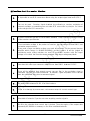
6.Check Point of Operation
Before power-up, please make sure that the connections are
no problem.
Caution!
6.1 Check Point for Resolver Interface
6.1.1
Check Point of Excitation Signal
Check your resolver excitation signals (R1, R2) whether the resolver is excited with your
designed amplitude or not. If signals are small or saturated situation, please check the
suitability of the load and excitation circuit which connect to AU6803(AU6804) excition output
terminal again. If there are no signals, please check the connection to resolver and power
supply status.
6.1.2
Check Point of Monitor Signal Amplitude
(1)Check point of amplitude change
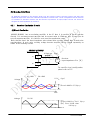
Observing the waveform of resolver exciting signals and monitor output (SINMNT、COSMNT),
please check if the monitor output have a same frequency carrier of excitation signals. After
then, rotate the resolver, please check that monitor signal amplitude is changing with
corresponding resolver angle. If there is no signal or no amplitude change by rotation, please
check the connection between resolver and AU6803(AU6804).
■Waveform example of exciting signal and monitor signal with some fixed angle
Electrical angle
0°
45 °
90 °
135 °
180 °
225 °
270 °
315 °
E xcit ation signal
SINMNT
COSMNT
Electrical angle
E xcit ation signal
SINMNT
COSMNT
- 40 -
xxxxxxxxxW00
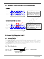
(2)Check point of amplitude level
Rotating the resolver with observing a monitor signal, please check the monitor signal (SINMNT
and COSMNT) maximum amplitude In case of 1.2~3.5Vp-p monitor amplitude range, you can get
specification performance of this product. If signal amplitude is not appropriate range, please
adjust your circuit constants of exciting amplifier and resolver signal input circuit.
E xcit aion
signal
SINMNT
1.2 ∼3.5Vp- p
1.2 ∼3.5Vp- p
COSMNT
6.1.3
Check Point of Phase Shift
Rotating the resolver with observing a exciting current output(R1-R2) of AU6803(AU6804)
and a monitor output voltage waveform, Please check the phase difference between a excitation
waveform component of R1-R2 current output and a excitation waveform component of the
output voltage monitor while both measurement signals are same phase. And measuring phase
difference must be inside below range of setting excitation-mode. When that is outside the
acceptable range, please set an appropriate excitation-mode to make phase difference inside
the acceptable range.
Setting of excitation mode
Phase shift acceptable range
Current excitation mode(VMD= 0 )
+90°±45°
Voltage excitation mode(VMD= 1 )
0°±45°
※ Regarding AU6803(AU6804) definition of phase shift, please note that the current phase is a criteria and
it is not for voltage phase difference between excitation signal output terminals (R1-R2).
■How to check the current phase excitation output
When you check the current phase of AU6803(AU6804) excitation output(R1-R2) by
oscilloscope, please prepare current probe. Otherwise you can confirm it by the following
methods which fit for each excitation mode.
- 41 -
xxxxxxxxxW00
Caution!
If the R1 or R2 terminal is short-circuited to GND or the power
line(VRR/VCC/VDD etc) may cause damage. When the waveform
between R1 and R2 need to be checked, observe it as the
difference of each waveform. Never connect probe-GND directly
to the R1 or R2 terminal.
(1)In case of using direct excitation function(Current mode) of this product.
If R1/R2 lines have series resistance and schottky barrier diode to measure noise inflow from
resolver excitation line, you can measure the voltage phase across the resistor inserted in
series as the desired current phase. Then you can see the current phase with measuring the
voltage waveform across the resistor in series either.
∼
AU6803(AU6804)
V1
V2
∼
Voltage across the resistor
レゾルバR1 へ
R1
13
R2
∼
15
レゾルバR2 へ
∼Cf
AGND
V1- GND
E xample wave form
(AC c ou plin g)
V2- GND
(AC c ou plin g)
Cu rren t phase
( Voltage
ac ross
re sistor V1 -V2)
COSMNT- GND
(AC c ou plin g)
Phase diffe rence
※The above example is for the phase advance case of
voltage monitor signal.
- 42 -
xxxxxxxxxW00
the
(2)In case of using external amplifier to excite resolver.
An external excitation amplifier (either voltage-type and current-type) need input as voltage
source which is converted from exciting current output of AU6803(AU6804) by inserting a
resistor between R1 and R2 like below. Then this voltage phase of across the inserting resistor
is getting to be same as the desired current phase. So you can get the current phase with
measuring the voltage waveform across the inserting resistor.
∼
AU6803(AU6804)
∼
15
∼
To e xcitin g amplifie r
R1
Voltage across the resistor
13
R2
∼
E xample wave form
V1- GND
(AC c ou plin g)
V2- GND
(AC c ou plin g)
COSMNT- GND
(AC c ou plin g)
Cu rren t phase
( Voltage
ac ross
re sistor V1 -V2)
Phase diffe rence
※ The above example is for the phase delay case of
voltage monitor signal.
- 43 -
xxxxxxxxxW00
the
■How to convert an angle of phase shift
Cu rren t phase
COSMNT-GND
(AC c ou plin g)
Phase shift[°]=360[°]×(Time shift[μs]/Exciting frequency period[μs])
Above case:Exciting frequency=10kHz
Period=100μ(=1/10kHz)
Time shift =24μs
Phase shift=86.4° (=360×24/100)
6.2 Check Point for Digital Output
6.2.1
Check Point of Output Angle
Please check that the each digital output show your required format which you set and angle
output data is changing with resolver rotation. If angle output is not change while resolver
rotation or output format is different with your setting, please check a polarity of each digital
input terminal. Also if output angle data does not match with actual angle or output data is not
stable, refer section 6.1 and please check if there is no problem for resolver related
connections.
6.2.2
Check point of abnormality Detection
ERR
output and
ERRHLD
output should be both L-level for normal condition
while ERRSTB input is H-level. If this device detects some error condition, ERR output or
ERRHLD output will be H-level. Then you may refer section 9.1 and please isolate the true
cause of the error and remove it.
- 44 -
xxxxxxxxxW00
7.Built In Self Test(BIST)Function
AU6803 (AU6804 ) has a built-in self test function and you can determine the validity of
operation by excuting this BIST function sequence. The details of the diagnosis are described
below.
・BIST of R/D conversion:Self-diagnosis function of R/D conversion. It is self tested by
means of the electrical angles of 0, 45 or 270 degrees set as the resolver
signal input.
・BIST of failure detection:Self-diagnosis function of failure detection. Set the simulated
abnormal conditions and possible to determine the validity of the failure
detection operation. It include below.
■ BIST of Broken Wire : Self-diagnosis for the detection function of a
Breaking of Resolver Signal Line
In this section, we explain the operation, how to excute, and diagnostic results of BIST.
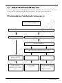
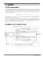
7.1 Run-Time Behavor of BIST
BIST functions test to determine the validity of the failure detection function by generating a
required failure signal inside IC and monitoring the output signal. While each BIST is executing,
device operations which is R/D conversion and failure detection are switched to work on
simulated signal base. Then please note that normal operation using external resolver input
signal becomes invalid while excuting BIST.
■BIST circuit schematic configuration
Resolver signal input circuit
Normal resolver signal
R/D conversion
circuit
Simulated signal
generating circuit
Failure detection
circuit
BIST
Result and
judgement
BISTVLD
BIST setting
- 45 -
xxxxxxxxxW00
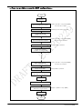
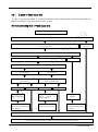
7.2 Execution Method of BIST
BIST function is active when BISTVLD input is Low . And BIST will be excuted while
configuration registers (Bit No 7~10) has been set. The result can read by serial output BIST
code (BISTCD1~BISTCD4) when BIST is excuting. The following shows the basic execution flow.
■ BIST excution flow
―If you run only a specific set BIST.―
St art
BISTVLD= L
BIST settin g
(Se rial c onfigu ration re giste r)
Switch t o BIST operation
Re giste r: [Bit No.7 ∼10 ]=exce pt [0000 ]
Switchin g from normal ope rat ion
Reads BIST resu lt s
(BISTCD of se rial out put)
BISTVLD= H
Switch t o n ormal ope ration
BIST un set
(Se rial c onfigu ration re giste r)
Re giste r: [Bit No.7 ∼10 ]=[0000 ]
E rror re set
En d
※ The order is not issue for BISTVLD=L switching and BIST setting . The reverse case, switching to
BIST operation is getting valid by BISTVLD=L switching .
※ The order is not issue for BISTVLD=H switching and BIST unset . The reverse case, switching to
normal operation is getting valid by BIST unset .
- 46 -
xxxxxxxxxW00
―If you run multiple consecutive BIST configurations―
St art
BISTVLD= L
BIST settin g
(Se rial c onfigu ration re giste r)
Switch t o BIST operation
Re giste r: [Bit No.7 ∼10 ]=exce pt [0000 ]
( The first se t of BIST)
Switchin g from normal ope rat ion
Reads BIST resu lt s
(BISTCD of se rial out put )
BIST settin g chan ge
(Se rial c onfigu ration re giste r)
Switch t o ne xt BIST
Re giste r: [Bit No.7 ∼10 ]=exce pt [0000 ]
( The sec on d set of BIST)
Ch ange d BIST ope rat ion
Reads BIST resu lt s
(BISTCD of se rial out put )
BIST settin g chan ge
(Se rial configu ration re giste r)
Switch t o last BIST
Re giste r: [Bit No.7 ∼10 ]=exce pt [0000 ]
( The last set of BIST)
Ch ange d BIST ope rat ion
Reads BIST resu lt s
(BISTCD of se rial out put )
BISTVLD= H
Switch t o n ormal ope ration
BIST un set
(BISTCD of se rial out put )
Re giste r: [Bit No.7 ∼10 ]=[0000 ]
E rror re set
En d
- 47 -
xxxxxxxxxW00
■Considerations for BIST execution
When you perform BIST, please note the following points.
① Must be run with “INHB=High”.
② Please set more than 10ms latency for reading BIST result of BIST execution from normal
operation, and for reading BIST result of the BIST configuration changes under BIST mode.
③ After any BIST is completed and switch to normal mode, the external filter is reset once.
④ The error reset should be performed after any BIST is completed.
⑤ Please set more than 10ms latency to excute error reset after switching to the normal
operation mode from BIST mode.
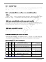
7.3 Result of BIST
Each BIST result indicate their specific code of BISTCD1~4 which is assigned as Bit3~6 of
serial output mode [11](Result of BIST). The diagnosis result that is falling edge timing of SCSB
output as serial data.
■Description of BIST results
BIST
CD4
BIST
CD3
BIST
CD2
BIST
CD1
Description of BIST results
0
0
0
0
(default value)
0
0
0
0
0
0
0
1
0
1
1
0
1
0
1
0
−
−
−
−
0
1
0
1
0
1
1
0
0
1
1
1
1
1
0
0
0
0
0
1
1
0
1
0
1
0
1
1
1
1
1
1
1
1
1
1
0
0
1
1
0
1
0
1
Matched to the BIST command angle
1(0°)
Matched to the BIST command angle
2(45°)
Matched to the BIST command angle
3(270°)
Remarks
Except duration of
BIST operation
Matching range:±1.4°
max
Matching range:±1.4°
max
Matching range:±1.4°
max
−
−
Normal operation for broken wire
detection BIST(COS signal line)
Normal operation for broken wire
detection BIST(SIN signal line)
−
−
−
Abnormal BIST
- 48 -
xxxxxxxxxW00
8.Function of Fault Detection
AU6803(AU6804) has built-in test function of fault detection. These error conditions output
at the ERR or ERRHLD terminal and error code which describe error contents output from
the ERRCD1~3 by output setting. The 4 kind of contents of detection are shown below.
・Abnormal Resolver Signal(Square-sum method)
・Break Detection of Resolver Signal Line(DC-bias method)
・Abnormal R/D conversion(PLL Unlock)
・Abnormal High Temperature inside IC
In this chapter, describe each detection method and typical fault detection pattern and also
describe corresponding error code, their priorities, and error reset method.
This built-in test function is independent from R/D conversion function and does not restrict
any output of R/D conversion IC as a result of this failure. However, when Resolver signal is
returned from abnormal resolver signal state or any breaking of line, the external filter(loop
filter) is reset once.
8.1 Abnormal Resolver Signal(Square-sum method)
8.1.1
Concept Detection
This concept is to detect fault status that monitor output amplitude balance is disturbed. In
case of shorted/breaking-down state of exciting line, resolver is not excited and signal will
disappear then this situation can detect as fault status. Also short circuit between signal lines
S1-S3, S2-S4), or rear short circuit of resolver winding, etc. may be detected if the state
satisfies the abnormality determination.
8.1.2
Circuit Configuration
Absolute
Square circuit
SINMNT
COMP.
Adder
Absolute
Square circuit
Inverter with
filter
Detection result
COSMNT
Selector
threshold(0.7Vp-p setting)
threshold(1.0Vp-p setting)
Serial input setting Bit12
- 49 -
xxxxxxxxxW00
8.1.3
Detection Principle
The detection principle is making comparison between threshold value and absolute square
sum value( | SINMNT |2 | COSMNT |2 ) of SINMNT/COSMNT output. If square sum value is getting
below the threshold, it is detected as fault status. And this threshold value can be changed by
updating of serial input setting register.
8.1.4
Relationship of threshold and Typical abnormal detection pattern
Monitor out V
(1)Normal
COSMNT envelope(kE 1 cos θ)
1.2 ∼3.5Vp-p
SINMNT envelope(kE 1 sin θ)
0.7Vp-p(typ.) or 1.0Vp-p(typ.)※
V C O M =2.25V
In normal monitor signal case,
absolute square sum value of
SINMNT/COSMNT always exceed
threshold, then it does not detect
as fault.
※By serial setting
Resolver electrical angle θ
Monitor out V
(2)Detection pattern①(Absolute square sum value of monitor is under threshold)
0.7Vp-p(typ.) or 1.0Vp-p(typ.)※
Breaking/down of exciting circuit
or smaller monitor output will
detect as abnormal signal in full
angular range.
※By serial setting
Resolver electrical angle θ
- 50 -
xxxxxxxxxW00
Monitor out V
(3)Detection pattern②(Shorted between S1-S3 or S2-S4)
※example: Shorted between S1-S3 case
0.7Vp-p(typ.) or 1.0Vp-p(typ.)※
In case of short between S1-S3 or
S2-S4, when normal signal amplitude go
under the threshold value, error can
detect in such angle range.
This range is under threshold
※By serial setting
Resolver electrical angle θ
8.2 Break Detection of Resolver Signal Line(DC-bias method)
8.2.1
Concept Detection
In the resolver signal input circuit, applying the external DC bias circuit(refer 4.2.2) will make
―――――
――――
the reverse-side DC level of internal resolver signal(C O S or S I N ) shifted from V CO M voltage
of reference potential to AGND side when resolver signal line is broken. And monitor output
signal shift from V CO M voltage to VCC side. Concept detection is to detect this DC level shift of
reverse-side of internal resolver signal.
【 In DC vie w: Normal- re solve r signal in put circuit】
【 In DC vie w: Breakin g- re solve r sign al in put circu it】
AU6803(AU6804)
AU6803(AU6804)
COSMNT
(SINMNT)
COSMNT
(SINMNT)
VCC
+
-
V CO M
RH
+
-
V CO M
RH
R IN /2
S1 (S2 )
VCC
R IN /2
R IN /2
S3 (S4 )
RL
R IN /2
S3
(S4)
-
CO S ( SIN)
+
CO S ( SIN)
In te rnal re sol ver sign al
AGND
R IN /2
RL
R IN /2
S3
(S4)
Detect ion
-
CO S ( SIN)
+
CO S ( SIN)
∼
R
R IN /2
S1
(S2)
∼
S1
(S2)
R IN /2
Detect ion
In te rnal re sol ver sign al
AGND
Re solve r DC 【R】 ≪ DC bias 【R B H or R B L 】. In this c ase,
Re solve r te rmin al S1/S3 (or S2/S4
) are ――――
same potential.
――――
Then inte rnal re solve r signal ( C O S or S I N ) is gett in g
to be re fe rence potential V CO M .
( Mon itor out put is also V CO M leve l of DC vie w. )
- 51 -
Breakin g line case, VCC-AGND en te red to diffe rent ial
amplifie r circu it in put. Then inte rn al re solve r signal
――――
――――
( C O S or S I N ) sh ift from refe rence V CO M voltage to
AG ND side.
( Mon itor out put sh ift to VCC side.)
xxxxxxxxxW00
8.2.2
Circuit Configuration
COMP.
COS or SIN
Integrator
Threshold
(1.85V DC typ.)
8.2.3
Detection result
Detection Principl
The principle is comparison between internal resolver signal voltage and threshold. If the time
which counts below the threshold is longer than the time(T L ) which exceeds the threshold, it is
detected as fault situation.
In monitor output case, if the time (T H ) which exceeds 2.65V D C typ is longer than the time (T L )
which counts below its voltage, it is detected as fault situation.
8.2.4
Relationship of threshold and Typical abnormal detection pattern
Monitor output V
(1)Normal
COSMNT or SINMNT waveform
V C O M +0.4V D C (typ.)
V C O M =2.25V
TH
In normal monitor signal case, both
SINMNT
and
COSMNT
show
“T H <T L “ situation then it does not
detect as fault.
TL
Time
Monitor output V
(2)Detection pattern③(Breaking between S1-S3 or S2-S4)
※Mounted the DC bias resistance
In case of breaking signal line, the
monitor output DC level will
exceed threshold value due to DC
bias resistance and this “T H >T L ”
situation can detect as fault.
Break
TL
TH
Time
- 52 -
xxxxxxxxxW00
Monitor out V
(2)Detection pattern④(Rectangle monitor output waveform)
When the monitor output is in a
rectangular wave to be saturated, it
will be “T H =T L ” condition then it
might be detected as fault situation
due to boundary conditions for the
determination.
TH
TL
8.3 Abnormal R/D conversion(PLL Unlock)
8.3.1
Concept Detection
Twin-PLL (refer chapter 1.3 or 11.1) which is a R/D conversion method of this product are
composed of two PLL. In normal conversion activity, by taking the difference of each PLL
output(ωt+φ, ωt-φ), it is possible to obtain digital data corresponding to resolver angle.
Also average value of each PLL output becomes to the excitation frequency and maintain the
certain relationship between each phase. This concept detection is to detect a state which the
average value of the output frequency of each PLL or a state which phase relationship has
collapsed. These conditions are defined as state that is not established normal R/D conversion
and they are detected as fault situation.
8.3.2
Circuit Configuration
PLL average out
PLL-Ⅰ out
(ωt+φ)
1/2
PLL-Ⅱ out
(ωt-φ)
Phase
/frequency
comparison
Judgement result
Exciting counter
(ωt)
8.3.3
Detection Principl
The principle is to make comparison of phase and frequency between average value ※ (counter
output) of the two PLL outputs and exciting counter output ※ which is the counter output for
generating an excitation signal. When the frequency has become a mismatch or phase
relationship has collapsed, it is detected as fault.
※ These output signals can not be verified from the outside of this product.
- 53 -
xxxxxxxxxW00
8.3.4
Relationship of threshold and Typical abnormal detection pattern
(1)Normal
PLL
In normal R/D conversion state,
PLL average output value and
exciting counter output (frequency)
are matched. Also phase maintain a
certain relationship. Then it is not
detect as fault.
average
output
Exciting counter
output
Time
(2)Detection pattern⑤(PLL unlock)
Mismatch
PLL
When
PLL
unlocked
and
R/D
conversion is not performed normal,
the phase relationship between PLL
average output and exciting counter
output has changed and frequency is
getting mismatched. Then it is
detected as fault situation.
average
output
Exciting counter
output
Time
8.4 Abnormal High Temperature inside IC
8.4.1
Concept Detection
In this detection concept, a state which the IC junction temperature exceed 150℃ is defined
as a state leading to product failure, then it is detected as fault. The product which is
detected as this abnormal high temperature might be damaged their circuit by heat even back
to the normal state. So please do not use such products.
8.4.2
Circuit Configuration
COMP.
Temperature-dependent
voltage inside the IC
Detection result
Threshold
(Roughly equivalent to
more than 150℃)
- 54 -
xxxxxxxxxW00
8.4.3
Detection Principl
The principle is to make comparison between the generating voltage which characteristic
depend on the temperature at the internal and threshold voltage which equivalent to more than
150℃. If it exceeds the threshold temperature it is detected as fault.
8.4.4
Relationship of threshold and Typical abnormal detection pattern
(1)Normal
If device usage is inside of specified operating temperature (ambient temperature), power
derating, and voltage, it is not detected as fault as long as the product is not defective.
(2)Detection pattern⑥(outside condition usage against specified)
There might be possibility to detect as fault in below state, loss exceeds the allowable state or
ambient temperatures above 125℃, load larger than the specified connection or larger than the
specified voltage, in the situation raises heat departing from the specification.
(3)Detection pattern⑦(IC Corruption)
If there is a situation such as excessive current flows through the internal IC due to some
failure, it might be detected as fault.
8.5 Fault Detection Contents and Error Code
Error code was assigned for each fault. When fault is detected, error state output from
ERR and ERRHLD terminals and ERRC1~3 will be output from the contents detected as an
error code. In case of simultaneous errors, only the error code with priority is indicated.
■Error code(Result of failure detection)list
ERR
CD3
ERR
CD2
ERR
CD1
Description of Error
(Result of failure detection)
Priority
※
Remarks
0
0
0
No abnormal state
−
No error output
0
0
1
Abnormal resolver signal(square sum)
3
0
1
0
Broken wire of resolver signal(COS line)
1
0
1
1
Broken wire of resolver signal (SIN line)
2
1
0
0
Abnormal R/D conversion(PLL unlock)
4
1
0
1
(Not defined)
−
1
1
0
1
1
1
Abnormal high temperature inside IC
(approxmately 150℃ or more)
Error mask when starting(After releasing
reset)
Out of Freq lock
5
−
※ Smaller numbers are getting higher priority.
- 55 -
xxxxxxxxxW00
8.6 Error Reset
The contents of ERRHLD and error code (ERRCD1~3) which is set by detecting fault is reset by
setting ERRSTB=Low .
■Error-reset operation waveform
ERRSTB
ERRHLD
ERRCD[3:1]
ERR
(Error state)
[000]
(Error state)
except[000]
[000]
(except[000]:error continue case)
(The broken line shows any error continued.)
※ For timing detail, please refer 10.9 .
※ The ERRHLD output should be used after the error is reset by the ERRSTB input. When the ERRHLD
output can not be released by the Error Reset, remove the true cause of error referring to the section
9.1.
- 56 -
xxxxxxxxxW00
9.If you think trouble shooting
In this chapter, there are corresponding examples for the case of error detected by the
function of fault detection, and for the case of strange angle output data. Please check these
examples for your troubleshooting and operation check.
9.1 In case of error detection
When an error is detected (ERR or ERRHLD output are H level), refer to the following
troubleshooting flow. Firstly please perform to estimate reason of fault detection, and error factor
should be identified and eliminated according to the procedure of chapter 8.1.1 or lator. Regarding
the operation of fault detection function, please refer chapter 7.
■Troubleshooting flow of error
Error detected
Whether error code can be identified or not?
Identified
Not be identified.
When an error is detected, please caliculate the square sum of the SINMNT/COSMNT.
Then please check whether the data is below the threshold or not.
Below threshold
Above threshold
At error, please check whether DC level(amplitude center ) is
above 2.65V D C (typ.) or not.
Please check error
contents by error
code.
Above 2.65V
Below 2.65V
Output data match to resolver angle?
Go to applicable
contents of
following
9.1.1∼9.1.4
Mismatch
Match
Abnormal resolver
signal
Break detection of
resolver signal line
Abnormal R/D
conversion
Abnormal high
temperature
To 9.1.1
To 9.1.2
To 9.1.3
Refer 8.4
- 57 -
xxxxxxxxxW00
9.1.1
Suspicion of Abnormal Resolver Signal (Square-sum method)
In case of suspicion of abnormal resolver signal (square-sum method) detection, true error
factor should be identified and eliminated according to the below troubleshooting flow.
■Troubleshooting flow of abnormal resolver signal
Detection by abnormal resolver signal(square-sum)
Please check the signal waveform of R1/R2 excitation output terminal of this product( refer 6.1.1)
Almost no signal
amplitude
Square wave or
saturated.
Excessive connection
impedance or possible
excitation line breaking.
Please check the
connection status of the
load between R1-R2.
Center of signal is
near VCC or GND.
Expected sine wave (No problem)
Possibility of GNDshort or VCC-short.
Check possible short
between R1/R2 and
VCC/GND line.
External excitation amplifier exist?
Please make sure there is no short circuit between R1-R2.
No short
Short exist
There is an external
excitation amplifier.
No external Amp.
Direct resolver excitation
with built-in amp.
What is clock status?
Ple ase improve ment.
Please check the excitation signal
waveform at resolver exciting terminal.
No signal
Possibility of
mis-configuration
Clock might not be
applied.
Review
default
setting and update
serial input setting
register (Bit 2).
Please make sure
that
clock
is
applied
successfully.
Break/down of
exciting line
Normal signal
Detect fault by the resolver signal.
Please check the connection of
exciting line or the state of
the amplifier power supply
line.
- 58 -
Go to next page.
xxxxxxxxxW00
Detect fault by the resolver signal(Continue from previous page)
When the resolver rotation, please check whether SINMNT/COSMNT amplitude change or not.
(refer 6.1.2(1))
Amplitude is changing.
Certain amplitude but no
change
Please adjust the level of the
monitor output (refer 4.2.2)
Please check the connection
status.(refer 5.1)
- 59 -
One monitor looks OK but
other one have no amplitude.
Please make sure not short
circuit between each signal line
or aginst power line.
xxxxxxxxxW00
9.1.2
Suspicion of Break Detection (DC-bias method)
In case of suspicion of break detection of resolver signal line (DC-bias method), true error
factor should be identified and eliminated according to the below troubleshooting flow.
■Troubleshooting flow of detecting break of resolver signal line.
Detection by break of resolver signal
line (DC-bias method)
Please check whether center amplitude of SINMNT/COSMNT shift from 2.25V to VCC side.
Has shifted
Not shifted.
SINMNT/COSMNT waveform might be rectangular shape.
(Detection pattern④)
Please check that resolver signal input circuit has correct gain
setting and monitor output shows under 3.5Vp-p.
Signal line breaking.
(Detection pattern③)
Above 3.5Vp-p
Please make sure about
resolver signal line
connections and conduction
between the S1-S3 and the
S2-S4.
Please adjust the level of the
monitor output
(refer 4.2.2)
- 60 -
Under 3.5Vp-p
Checl the resolver interface
circuit and eliminate/improve
the factor of rectangular
shape monitor output.
xxxxxxxxxW00
9.1.3
Suspicion of Abnormal R/D conversion (PLL Unlock)
In case of suspicion of abnormal R/D conversion (PLL unlock), true error factor should be
identified and eliminated according to the below troubleshooting flow.
■Troubleshooting flow for abnormal R/D conversion detection
Abnormal R/D conversion
(PLL unlock)
detected.
Please make sure whether absolute angle data is settled or not.
Not settled.
Only MSB has been non-settling.
Settles.
Due to inappropriate exciting mode setting,
possibility of phase determination has become a
NG cause of near edge of acceptance range.
Excitation mode setting can be checked by
serial output BIST mode VMD bit.
Please make sure whether you have set properly
pull-up/pull-down of terminal Z.
PLL unlock
(Detection pattern⑤)
Check
external
filter
connection ( LFUI/LFUO or
LFLI/LFLO )
whether
shorted or opened state
exist or not.
Inappropriate
Adequate
Improper handling of
pull-up/pull-down
state for terminal Z.
There is possibility of
mis-setting terminal Z
when the power is
turned on.
Possibility of angular
acceleration of the
resolver is too large
(exceed spec value).
Please check your system
carefully that there might be
input signal(other polarity of
setting) for terminal Z when
the power is turned on.
Please
rapid
angular
exceeds
Please
make
appropriate settings
for terminal Z.
- 61 -
avoid about
changes
in
velocity that
the spec.
xxxxxxxxxW00
9.2 In case of wrong angle data
Despite the rotating Resolver, angle output data is not changed, or output shows the different
format data, or output data is not fit to actual angle. In such case, please follow below
troubleshooting flow and identify the behavior of the output data. Then please improve this
error condition by the procedure described in chapter 9.2.1 and later.
■Troubleshooting flow of wrong digital angle data.
Wrong digital angle output
Please check the behavior of the output data during one Resolver rotation.
Output data fixed.
To 9.2.1
Indefinite, free run,
or can not get
one-rotation data.
Wron g rotate direction・
90°deviation・
180°deviation
Rapid changes in
disturbance data
(A/B pulse sudden
disturbance)
To 9.2.2
To 9.2.3
To 9.2.4
- 62 -
xxxxxxxxxW00
9.2.1
In case of fixed angle data
In case of angle output data is completely stopped, please follow below troubleshooting flow and
identify the factors, and then improve your system.
■Troubleshooting flow of fixed angle data
Angle output data is completely stopped
Whether the fixed output data of interest is INHB target signal or not?
Target signal
(φ1∼12、U, V, W)
Out of target
(A, B, Z)
Please check the polarity of the input INHB .
H-level
L-level
What type of output that is stopped?
Palallel output
Serial output
Please check the polarity of the
input CSB .
Please check whether SCSB/SCK
input is appropriate?
H-level
L-level
This is output
High-Z setting.
Change CSB to L-level,
and check whether data
can change.
Inappropriate
Adequate
Possibility of output
High-Z
setting,
or
stopped state.
This is data fixed
setting.
Apply the appropriate
serial output sequence.
Change INHB to H-level,
and check whether data
can change.
There is the possibility of running the BIST function.
If you are performing a BIST, please return to the normal operation mode.
- 63 -
xxxxxxxxxW00
9.2.2
In case of indefinite, free run, can not get one-rotation data
In case of angle output data is indefinite, free run, can not get one-rotaion data, please follow
below troubleshooting flow and identify the factors, and then improve your system.
■Troubleshooting flow of indefinite, free run, can not get one-rotation data
indefinite・free run・can not get one-rotation data
Please check whether error occurs or not.
Error occurs.
Error does not occur.
What is behavior of the data?
May be abnormal
resolver signal,
breaking signal line,
or abnormal R/D
conversion.
Data is indefinite.
Data is free run.
(Keep rotation.)
Can not get one-rotation data.
Possibility that the
output has been
disabled.
Possibility of
abnormal R/D
conversion.
Possibility of different output mode.
What type of output are you using?
Refer chapter 8.
Refer 8.3.
What type of output are you using?
Parallel output
Please make sure
the CSB input
polarity.
Serial output
Please make sure
the SCSB input
polarity.
Parallel output
Serial output
How to define output mode?
Default setting
Please check your system
carefully that there might be
input signal (other polarity of
setting) for terminal ERRHLD
when the power is turned on.
- 64 -
Serial setting
Please check the current output mode
by serial callback and try the serial
setting again if it is different mode
against you desired.
xxxxxxxxxW00
9.2.3
In case of rotation direction difference, 90°deviation or 180°deviation
In case of angle output data shows rotation direction difference, 90 ° deviation or 180 °
deviation, please follow below troubleshooting flow and identify the factors, and then improve
your system.
■Troubleshooting flow of rotation direction mismatch, 90°/180°deviation
Rotation direction mismatch , 90°/180°deviation
Please check the situation. Is Rotation direction mismatched?
Rotation direction
mismatch
90°deviation
90°deviaton? 180°deviaton?
180°deviation
Wrong direction and
180 ° deviation at
0°resolver position.
Please make sure the resolver connection
of R2 or R1.
Reverse connection
Normal
Possibility of
incorrect excitation
mode.
Resolver signal
SIN pair reverse
connection
Resolver signal
SIN pair and COS
pair are reversed.
Resolver excitation
signal is reverse
connection.
Please make sure
whether S2/S4
connection is ok or
reversed.
Please make sure
whether S2/S4 pair
and S1/S3 pair
connects reverse or
not.
Resolver R1 and R2 Please make sure the
signals
must be relationship between
connected properly. excitation mode and
phase shift.
(refer
6.1.3)
- 65 -
Resolver signal
COS pair reverse
connection
Please make sure
whether S1/S3
connection is ok or
reversed.
xxxxxxxxxW00
9.2.4
In case of rapid change in the output angle data and disturbance
In case of rapid change in the output angle data or a sudden disturbance while rotation, please
follow below troubleshooting flow and identify the factors, and then improve your system.
■Troubleshooting flow of rapid change in the output angle data and disturbance
Rapid angle change and sudden disturbance while rotation.
Please check whether error occurs or not during constant angular verocity rotation.
Error does not occur.
Error occurs
Please check whether SINMNT or COSMNT waveform has some
noise(waveform distortion) or not.
There is noise
(waveform distortion).
Looks normal.
May be abnormal resolver
signal, breaking signal line, or
abnormal R/D conversion.
Disturbance data by magnetic
noise
Might be instantaneous power
failure.
Refer 9.1 .
Identify the factors,
And improve system with
appropriate countermeasure.
Please check supply voltage
variation. Under 4.5V case,
need countermeasure.
9.3 If the situation does not improve
If the situation does not improve even if section 9.1 or 9.2 steps perform, and if there is
another phenomenon which does not mention in this manual, please contact us with waveforms
when an error occur (appropriate abnormal signal, SINMNT, COSMNT) and also inform us about
detail troubled circuit information.
- 66 -
xxxxxxxxxW00
10.Electrical characteristics
10.1 Absolute maximum rating
Items
Symbol
Absolute maximum rating
Unit
VCC
-0.3∼+7.0
V
VRR
-0.3∼+7.0
V
VDD
-0.3∼+7.0
V
Analog input voltage
V Ia
-0.3∼VCC(VRR)+0.3
V
Digital input voltage
VI
-0.3∼VDD+0.3
V
Digital output current
IO
-10∼+10
mA
Operating temperature
T o pr
-40∼+125
℃
Storage temperature
T stg
-65∼+150
℃
Allowable loss
PD
500
mW
Power supply voltage
※ If you use the IC beyond the absolute maximum rating, it may cause permanent damage to the IC.
10.2 Power-related characteristic
Items
Symbol Min.
VCC
Power supply voltage
4.5
Typ.
Max.
Unit
5.0
5.5
V
Remarks and conditions
Recommended power supply voltage.
VCC, VRR, VDD must be used at the
same potential.
VRR
4.5
5.0
5.5
V
VDD
4.5
5.0
5.5
V
Reset release voltage Vrsth
3.9
-
4.4
V
Power-On-Reset release voltage
Reset voltage
Vrstl
3.7
-
4.2
V
Power-On-reset voltage
Reset voltage hysteresis
Vrhys
-
0.2
-
V
Vrsth-Vrstl
IC C1
-
-
45
mA CSB=H/Supply current at static angle※
IC C2
-
-
50
mA
IC C3
-
-
60
Supply current
CSB=H/Maximum rotation or
CSB=L/supply current at static angle※
CSB=L/Supply current at maximum
mA
rotation※
※ Internal current consumption of the digital output at no load, include exciting current.
- 67 -
xxxxxxxxxW00
10.3
R/D conversion characteristic
Items
Symbol Min.
Typ.
Resolution
Max.
Unit
Remarks and conditions
Bit
A number of divisions per electrical
angle.
12
Conversion accuracy
-4
-
4
LSB
Absolute error of the electrical angle
input in a stationary state.
Repeatability
-2
-
2
LSB
Repeatable angle accuracy
ms
Input step of 180°electrical angle
Settling range:±8LSB max.
Settling time
1.5
Maximum angular
velocity 1
240,000
min -1
Maximum angular
velocity 2
180,000
min -1
Maximum angular
acceleration
1,000,000
rad/s 2
Responsibility
-0.2
0.2
Stabilizing time at
start
10MHz < Ext-CLK ≦ 12MHz
Angular velocity range capable of
tracking in the electrical angle.
8MHz < Ext-CLK ≦ 10MHz、or
internal clk operation mode. Angular
velocity range capable of tracking in
the electrical angle.
Angular acceleration range capable
of following.
Output response delay in a constant
deg./
angle velocity.
10,000min - 1
(Equivalent to 3.3μs)
20
ms
Stabilizing time of output at start.
(±8LSB max at static state)
10.4 Built-In Self-Test(BIST) characteristic
items
Symbol Min.
Typ.
Max.
Unit
Remarks and conditions
R/D conversion BIST(0°/45°/270°)
Determination
threshold
-1.4
-
1.4
deg.
Allowable range for the setting angle.
Determination time
-
-
10
ms
The time required to stabilize BIST
results.
10
ms
The time required to stabilize BIST
results.
Failure detection BIST(Broken wire BIST)
Determination time
-
-
- 68 -
xxxxxxxxxW00
10.5 Failure detection characteristic
Items
Symbol Min.
Typ.
Max.
Unit
Remarks and conditions
Vp-p
Setting register Bit12 = 0 case. The other
voltage amplitude when any one of monitor
output is 0V.
Abnormal resolver signal(Square sum method)
Detection threshold 1
Detection threshold 2
Relative
range
deviation
between
Determination time
0.5
0.7
0.9
0.8
1.0
1.2
Vp-p
Setting register Bit12 = 1 case. The other
voltage amplitude when any one of monitor
output is 0V.
0.2
0.3
0.4
Vp-p
Threshold_2 – Threshold_1
-
-
2
ms
Time required detecting fault.
Broken wire of resolver signal(DC bias method)
Detection threshold
0.33
0.4
Determination time
-
-
0.5
10
V
ms
DC level variation of monitor
output voltage.
Time required detecting fault.
※ In case of the continuous time of failure is shorter than above detection time, there is possibility not to
detect failure.
- 69 -
xxxxxxxxxW00
10.6 Analog signal characteristic
Items
Symbol Min.
Typ.
Max.
Unit
8.08
9.5
10.92
mArms.
8
10
12
kHz
Remarks and conditions
Excitation output
Output current
Output frequency 1
f CL K /
1024
Output frequency 2
Load impedance
Hz
200
Ω
Frequency range when using
the internal clock
Frequency by external clock.
(fCLK= external clock frequency)
Allowable load impedance of
R1/R2.
Resolver signal input
Input protection resistor
Input amplifier feedback
resistor
Relative accuracy of above
resistor
RF
Career gain
-
180
-
Ω
37.8
41.5
45.2
kΩ
-1
-
1
%
-20
-
20
%
The variation of monitor output
voltage when resolver is directly
excited by the R1/R2 of this IC.*
V
SINMNT, COSMNT terminal center
voltage.
Resolve signal monitor output
Internal reference voltage
V C OM
2.25
Max output amplitude
3.5
-
-
Vp-p
Load impedance
20
-
-
kΩ
7
10
12
μV/min-1
Allowable load impedance of
SINMNT and COSMNT.
Velocity output
Signal value 1
Setting register Bit11 = 0 .
Signal value 1
Temperature cofficient
-
0.025
-
(μV/min-1)
/℃
Signal vlue 2
70
100
120
μV/min-1
Signal value 2
Temperature cofficient
-
0.25
-
(μV/min-1)
/℃
Max output voltage range
3
-
-
V
VELP-VELN
output voltage
Output voltage offset 1
-0.2
-
0.2
V
Setting register Bit11 = 0.
Output voltage offset 2
-2
-
2
V
Setting register Bit11 =1.
Load impedance
20
-
-
kΩ
Setting register Bit11 =1 .
differential
Allowable load impedance of
VELP and VELN
※ Except the tolerance of input resistances and the performance of resolver itself.
- 70 -
xxxxxxxxxW00
10.7 DC characteristics of digital signal
Items
Symbol
Min.
Typ.
Max.
Unit
High level input voltage
V IH
2.0
-
VDD
V
Low level input voltage
V IL
0
-
0.8
V
Input hysteresis voltage
VH
-
0.2
-
V
Input pull-up resistance 1
Recommended input “H” voltage
for all digital input terminals.
Recommended input “L” voltage
for all digital input terminals.
Pull-up resistor value of digital
input terminal.
kΩ ※Applicable terminals
BISTVLD, CLKIN, SSDT, SSCS,
SCSB, SCK, INHB, ERRSTB, CSB
Pull-up resistor value of digital
input terminal.
kΩ
※Applicable terminals
ERRHLD, ERR, Z
30
50
85
Input pull-up resistance 2 R PU BI
72
120
200
Input leakage current
-
-
-200
VDD-0.1
-
-
V
I O H =0mA。
VDD-0.5
-
-
V
I O H =-4mA。
-
-
0.1
V
I O L =0mA。
-
-
0.5
V
I O L =8mA。
High level output voltage
Low level output voltage
R PU
Remarks and conditions
IL
μA V I =DGND。
V OH
V OL
10.8 AC characteristics of digital signal
Items
Symbol
Min.
Typ.
Max.
Unit
F CLK
8
10
12
MHz
External CLK duty
D CL K
40
-
60
%
Serial CLK input frequency
F SC K
-
-
5
MHz
Input rise-up time
tri
0
-
1.0
ms
Input fall-down time
tfi
0
-
1.0
ms
Output rise-up time
tr
-
4.2
7.3
ns C L =15pF。
Output fall-down time
tf
-
2.5
4.5
ns C L =15pF。
tpd
-
5.3
9
ns
tpd
-
4.7
9
ns C L =15pF。
External
frequency
CLK
input
Transmission delay time
(Input buffer)
Transmission delay time
(Output buffer)
- 71 -
Remarks and conditions
xxxxxxxxxW00
10.9 Timing diagram
■ ON/OFF power sequence
VCC
Vrsth
(VDD & VRR are applied
at the same time)
Vrstl
Resolver signal
Initial
tracking
D0∼D11
Output valid
[Indefinite]
Error judged results
[ERR CD1∼3]
(Error mask)
ERRHLD,ERR,Z
Error judged results [???]
Output
Input
1ms(max)
20ms(max)*
0ms(min)
70ms(max)
*:20,000 min -1 MAX. (Electrical angle)
■ Timing of Bus Control
CSB
INHB(RD)
φ1∼φ12
Fixed
Fixed
PRTY
PRTY
PRTY
40ns(max)
65ns 20ns
(max) (max)
- 72 -
30ns(max)
40ns(max)
10ns(min)
xxxxxxxxxW00
■ Serial input setting sequence
100ns(min)
Update of setting register
SSCS
50ns(max)
SCK
SSDT
Bit 1
Bit 11
Bit 2
Setting content
Bit 12
(Update)
(Set data in the past)
100ns(min) 100ns(min)
100ns(max)*
*:Changing to absolute output mode is exception case.
Please refer section 4.3.2(2) P34 sequence.
■ Waveform of serial output
The data at this time is
transmitted in serial.
100ns(min) 100ns(min)
200ns(min)
SCSB
SCK
DATA
Bit 1
50ns(max)
50ns(max)
Bit 12
PRTY
50ns(max)
100ns(min)
- 73 -
xxxxxxxxxW00
■ Timing of Error Reset
10ns(max)
40ns(max)
0∼100ns
ERRSTB
ERRHLD
(Error state)
ERR
(Error released)
(The broken line shows any error continued.)
20ns(min)
■ Operating sequence of Built-in Self-test(BIST)
BISTVLD
BIST enabled
SSCS
Content of
setting register
[Bit No.7∼10]
[0000]
[0000]
BIST setting except[0000]
BIST operation flag
D0∼D11
BIST judged results
[BIST CD1∼4]
Normal operation
Normal operation
BIST operation
Default value [0000]
BIST judged results[????]
10ms(max)*
Default value [0000]
10ms(max)*
*:Only at stationary state
- 74 -
xxxxxxxxxW00
11.Appendix
11.1 R/D conversion principle
This product adopted Twin-PLL method as R/D conversion system, and it has been configured
by two PLL(Phase Locked Loop) configuration and a subtractor to obtain the relative phase
angle between the PLL output. Each PLL takes one of the negative feedback controls of
closed-loop configuration. A control deviation(ε) is shown in below equation, and it must be
controlled as normally 0 .
Control deviation : ε=sin(θ−φ)・sinωt
Here assuming ε=0 means θ=φ , then resolver analog angular signal can be converted
to digital phase angle of PLL output.
One PLL a proceeding phase angle of the output matches the analog resolver angle, and the
other PLL a delaying phase angle of the output matches the analog resolver angle. Then output
angle φ can be obtained by calculating the relative phase angle of the two PLL output, and
analog angle information can be converted to digital.
■Configuration of Twin-PLL method R/D converter.
- 75 -
xxxxxxxxxW00
【Explanation of concept】
An amplitude modulated resolver signals can think to be composed by signal components of 2
frequency.
Sin phase : sin
Cos phase : cos
sin t
sin t
1
cos( t
2
1
sin( t
2
1
cos( t
2
1
)
sin( t
2
)
)
)
In this R/D conversion of Twin-PLL method, One PLL follow the ( ω t + θ ) frequency
component and the other PLL follow the (ωt-θ) frequency component.
An amplitude modulated resolver signals are input to the R/D converter, and each PLL
generate control deviation (ε) which is subtracted after multiplied between input signal and
sine or cosine signal that is fed back from the output signal of each PLLs. The control deviation
(ε) is introduced into the VCO (Voltage Controlled Oscillator) through the compensator that
stabilizes the negative feedback loop and improves its performance. The VCO generates the
pulse frequency output in proportion to the input voltage and is applied to the counter after it
converts from analog to digital. Then we can get (ωt+θ) frequency PLL output and (ωt-θ)
frequency PLL output as digital value. These two PLL output has a positive and negative phase
of the excitation frequency ω ,
so the digital angle φ can be obtained by taking the
difference between these two PLLs digital output.
- 76 -
xxxxxxxxxW00
11.2 About the error of resolver system
Resolver system with this product causes an error against actual angular position by resolver
accuracy, this smartcorder accuracy, peripheral configuration error, etc. In this chapter, explain
the error sources of resolver system and general estimation method of total error.
11.2.1
Error sources
There are error souces of resolver system like the following.
Error sources
Resolver-side
sources
R/D-side
sources
Resolver error
(accuracy)
Static error of the resolver itself generated by
manufacturing variation,etc.
Resolver misalignment
Static error by mounting accuracy when user
install the resolver.
R/D static error
(accuracy)
R/D response
Static error of this product itself generated by
production tolerance.
12Bit tolerance:±4LSBmax..(E-Angle 0.35°)
This IC response delay generates error
according to the angular velocity.
(Delay at constant angular
velocity)
0. 2
[min 1 ]
(E
10,000 min 1
Angle )
Resolver signal input
circuit. Resistance
accuracy
Static error by amplitude imbalance between
SIN input and COS input.
Resolver signal input
circuit.
Filter time constant.
Filter delay (time constant) generate an error
R-Relative accuracy1%>error 0.3°(E-Angle)
according to the angular velocity.
[s]
Environmental
factor
max .
External magnetic field
- 77 -
[min 1 ]
360(E
60[ s ]
Angle )
External magnetic field affects the flux of the
resolver and it cause error.
xxxxxxxxxW00
11.2.2
Error estimates
Total error of the resolver system using this IC is a combination of potential errors which
include static error that typically come from resolver itself or this IC itself, and proportional
error of angular velocity that come from delay of this IC or peripheral circuit depending on the
angular velocity.
εTTL εST εDLY ・・・
While ε TTL :Total Error of resolver system
ε ST :Static error of resolver system
ε DL Y :Angular velocity proportional error
※
Each error might have different unit, and there are concepts which are
Mechanical angle , Electorical angle . (Refer section 11.4 for each term).
error, please be careful to fitting the unit.
Number of multiple ,
When estimating the
■Estimation of static error
Considering the estimation method of resolver system static errors which include resolver
accuracy and error of this IC itself and the variation of the peripheral circuit or configuration,
the easiest way is taking the sum of the maximum error caused by factors. But it is difficult to
assume a probability that all of errors will be worst value, considering process capability, etc.
Also it might need excessive precision characteristic to satisfy system, and then system cost
might lead to increase.
Then static error of resolver system estimates normally with root mean square (RMS) method.
εST
(εR ) 2
While ε ST
εR
εS
ε RD
εi
(εS ) 2
(εRD ) 2
(εi ) 2・・・
:Static error of resolver system
:Error of resolver
:Error of resolver misalignment
:Static error of this IC itself
:Resolver signal input circuit :Resistance accuracy
■Estimation of angular velocity proportional error
Angular velocity proportional error of resolver system is caused by response delay of this IC and
signal delay which depend on the filter circuit constructed in resolver input circuit. This error is
getting bigger with higher angular velocity, and it is obtained by converting the angular displacement
from total delay time at applied angular velocity. Then it is estimated as the sum of individual errors
due to the delay factor.
εDLY
εRDDLY
εFLTDLY ・・・
While ε DLY :Angular velocity proportional error of resolver system
ε RDDLY :Angle error of this IC response delay
ε FLTDLY :Angle error of the filter time constant at resolver
signal input circuit.
- 78 -
xxxxxxxxxW00
11.3 FAQ
■Questions on the performance・characteristic of R/D conversion
Q
How much time it takes to convert R/D?
A
Assumed as delay time from input of resolver signal to output of its angle data.
Then it will be 3.3μs max. Response spec is converted value from above time
to the angular displacement while constant speed of rotation.
Q
Please tell us a frequency response of negative feedback loop which realize R/D
conversion.
A
When the recommended value of spec is applied between LFLI-LFLO and LFUI-LFUO,
bandwidth of this control system shows about 2.2kHz. A response that input angle
change at higher frequency than 2.2kHz will have -40dB/dec characteristic.
Q
What happen to the output data in case of resolver signal input is above maximum
angular velocity?
A
An absolute angle data can follow over spec velocity as long as the internal VCO
output is not saturated, but a change in the data will not be only one LSB. Along with
this A/B/Z output might generate missing pulses. When the rotation speed is getting
faster and the internal VCO output is saturated, it will not be able to follow the
rotation of resolver and output shows irrevant data (loss of synchronism condition).
Q
What is settling time?
The time to respond when resolver signal input change as step-like 180°. This is one
of the indicators which show control system performance of R/D converter.
There is no chance to work this step(180°) response for the actual resolver signals.
An gle
Se ttlin g time
A
180 °
0°
Time
0
- 79 -
xxxxxxxxxW00
Q
In the operation of the rotating resolver, output angle data against actual resolver
angle is shifted with the direction of rotation. Are there any considerable factor?
Typical factors are following.
(1) Displacement of the device which put on the resolver.
There might become angular displacement depending on direction, caused by
mechanical misalignment of device like backlash of gear, etc. The problem of this
factor is only depending on the rotation direction, and it is not depend on revolution
speed of resolver.
A
(2) Time constant of filter circuit.
If resolver signal input to AU6803 ( AU6804 ) through filters, there might show
angular displacement depending on rotation direction while high speed resolver
operation, caused by time constant delay value of filter circuit. The problem of this
factor normally tends to be large in proportion to the number of revolution.
(3)AU6803(AU6804)response (Delay time of response):
Delay time from resolver signal input to corresponding angular data output might
cause of the deviation angle which depend on the direction at high speed resolver
operation. The problem of this factor normally tends to be large in proportion to the
number of revolution.
Q
While we have connected the filter to the outside of LFUI, LFUO, LFLI, LFLO pins,
Why do we need these parts? For what?
A
It is configured the compensator for stabilization and improvement of the
characteristics of negative feedback control system. If not, the negative feedback
control system will be collapsed and it can not operate R/D conversion successful.
- 80 -
xxxxxxxxxW00
■Questions about the resolver interface.
Q
Is it possible to use R/D converter without using the output signal terminal R1/R2 ?
A
Can not be used. Resolver signal obtained by performing a resolver excitation of
external oscillator or something can not make R/D conversion in principle. So it does
not be subject for R/D conversion.
Q
A direct excitation function of the AU6803(AU6804) output can not generate voltage
of the resolver specification.
A
Direct excitation voltage is the product of resolver input impedance (below 200Ω) and
excitation output current.
If you need a larger excitation voltage, you need to excitation via the external booster
amplifier which source is AU6803 ( AU6804 ) exciting output. It will be judged by
considering noise effect whether we need to excitation resolver with the larger
voltage or not. And it will not be always required such larger voltage amplitude.
Q
How does this affect you connect a load of more than 200Ω between R1-R2?
A
There will be assumed that enough current can not flow in, the excitation signal is
saturated, can not get normal waveform. In addition, signal amplitude will be smaller
than the calculated value due to saturated signal.
Q
If e make short between R1-R2, IC will be broken?
A
There is no damage by overcurrent, etc because output is current control type.
Q
What kind of behavior if you do not enter anything resolver signal?
A
It will be the situation that control loop is broken. Then the angles of the output data
repeatedly UP/DOWN or runaway, so it will be undefined behavior.
- 81 -
xxxxxxxxxW00
Q
Please tell the voltage specification of S1~S4 input signals.
A
Input signal voltage range of each terminals must be 0~VCC as absolute maximum
rating. A operation acceptable range will be about 1.1V~3.8V (reference value) and
normally it works around 2.25V.
For the signal level adjustment of operational setting, instead of adjusting terminal
S1~S4, please adjust SINMNT/COSMNT voltage level which is 2Vp-p(typ) with COM
potential center.
Q
As a noise countermeasure, would like to add normal-mode-capacitor C N
How much capacitor value do you recommend?
A
C N insertion is required as counter action for some negative effect of electorical noise
injection. Actual cap value can not specify due to it depend on the noise level.
Too large cap value might cause larger attenuation and phase change of resolver
signals. So C N value variability might cause an imbarance between SIN and COS, and it
becomes error factor. Be careful about it.
Q
In case of monitor output exceed 3.5Vp-p, what kind of adverse effects can we
expect?
A
It is assumed like voltage saturation and abnormal waveform for monitor output.
These will be error factors for R/D conversion.
Q
Would like to monitor analog velocity output by analog port of microcontroller.
But there is a big offset exist and can not be used it.
A
Analog velocity output shows large variation and bigger influence of the temperature.
So it might use to check only standard level.
Then please understand that we can not recommend using this signal for speed
control, etc.
- 82 -
.
xxxxxxxxxW00
■Questions about the default setting function.
Q
Trying to set the default setting terminals for pull-up side.
The default setting terminals have internal pull-up resistor. Still do we need to add
external 10kΩ pull-up resistor for setting pull-up side?
A
In functiobnal view point, the terminal will be pull-up setting without external 10kΩ
pull-up resistor.
But internal pull-up resistor value of IC is large one so in terms of noise immunity it is
weak. Then we recommend to add external 10kΩ pull-up resistor.
Q
There is an excitation mode selection in default setting function. What is difference
between current excitation mode and voltage excitation mode?
An excitation mode setting function sets the allowable range of the internal phase
shift according to the phase shift value caused by the situation of the peripheral
circuits. This IC s acceptable range of the phase shift between an excitation
waveform component of R1-R2 current output and an excitation waveform component
of the output voltage monitor is as follows.
A
■Current excitation mode : +90°±45°
■Voltage excitation mode :
0°±45°
A main impedance of resolver will be L component and depending on excitaion type
there will be different phase value between an excitation waveform component of
R1-R2 current output (source of excitation signal) and an excitation voltage phase.
That is why we provided this function.
Since this is a function to change the internal setting, excitation output between
R1-R2 is not changed by this setting difference.
Q
Are there any effects when we used a situation which exceeds the allowable range for
each phase shift in the excitation mode setting?
A
There might be 180°inverted data despite the fact that there is normal resolver
configuration.
- 83 -
xxxxxxxxxW00
■Questions about the serial input setting function.
Q
While setting the serial, what happen in the situations which send only (ex) 8 bits data
and SSCS set to H ?
This is a shift register so newly input data update Bit12 value and existing data are
shifted to neighbor register which have smaller number.
Let s assume that when you enter up to 8 Bits. Input data (First Bit to last 8 th Bit)
enterd serial setting register Bit5 to Bit12. And remaining set of Bit1~4 contents was
8 bit shifted from previous Bit9~12 contents.
A
<Serial configuration register contents before updating>
Bit1 Bit2 Bit3 Bit4
Bit5 Bit6 Bit7 Bit8
Data Data Data Data Data Data Data Data
A
B
C
D
E
F
G
H
Bit9
Data
I
Bit10
Data
J
Bit11
Data
K
Bit12
Data
L
<Contents of register after setting 8 Bits serial data>
Bit1 Bit2 Bit3 Bit4
Bit5 Bit6 Bit7 Bit8
Data Data Data Data Data Data Data Data
I
J
K
L
M
N
O
P
Bit9
Data
Q
Bit10
Data
R
Bit11
Data
S
Bit12
Data
T
8 Bit s se rial in put data
Before Bit9 ∼12 dat a
Q
While setting the serial, what happen in the situations which send longer bits (ex: 16
bits) data and SSCS set to H ?
This is a shift register so last 12 input data was set in 12 shift register. Other data
before last 12bit data is discarded.
A
Let s assume that when you enter up to 16 Bits. The contents of 5Bit ~ 16Bit input
data can be set in serial setting 12 bit register.
- 84 -
xxxxxxxxxW00
■Questions about the output interface.
Q
A
In the situation of digital output terminals might be shorted each other , short to VDD
or GND, what kind of issues will be appear when the power is active?
When the voltage is different between the shorted pin (One side H and the other
side L ), excessive current flow from H to L , heating up, and finally IC might be
damaged.
Q
Would like to get 8bit parallel output data. How can I do?
A
AU6803 ( AU6804 ) have only 12bit-mode setting. If you ignore the lower 4 bits,
remaining data looks like 8 bits.
Q
There might be 1LSB difference between parallel data and serial data even if they
captured at the same timing. Why does it happen?
A
It caused by the different latch timing to get data internally.
Update timing of the serial output data is half cycle of the update for the parallel
output data. Then there might be 1LSB difference even if captured at the same time
according to the relationship of data capture cycle and data update timing.
Q
Is A/B/Z output from the parallel data pin (Pulse equivalent to encorder mode) the
same as A/B/Z output of independent terminal? Is it possible to be used at the same
time also?
A
It is the same output. And it is also possible to use at same time.
Q
Using encorder equivalent pulse mode, A/B pulse duty looks unstable while resolver
rotate with same speed. What is possible cause?
A
Encorder equivalent pulse output of this IC is theoretically poorer performance than
optical encorder pulse output. Due to the affect of resolver potential error and R/D
potential error and also R/D conversion principle itself, it is possible to be disordered
pulse duty even if in normal operation condition.
- 85 -
xxxxxxxxxW00
Q
For the digital output, serial interface output and parallel interface output and also
independent terminal A/B/Z output are prepared. Do we need to use all output?
A
On the behavior of this product it is not a problem even if it uses the output of either.
According to the system environment, please use appropriate interface or output.
Q
In serial output case, after SCSB falling edge, is the data which is before first SCK
falling edge unnecessary?
No need.
After SCSB falling edge, output data which shows until SCK falling edge is undefined
value. Please ignore it.
A
SCSB
SCK
DATA
Bit 1
Un defined
Q
To read the serial output data with above system, which is better trigger? SCK rising
edge or SCK falling edge?
Please use SCK rising edge.
Serial output data change with SCK falling edge timing. Then if you read the data with
SCK falling edge, there might read false data depending on read timing.
A
SCK
DATA
DATA switch t iming
- 86 -
xxxxxxxxxW00
Q
Plan to use serial output function with absolute output mode. But data need only 8bit
due to above system configuration. How should I handle about serial output data?
Please exit serial output sequence (SCSB=L⇒H) after 8 th serial data output.
※
Even in the middle to end, data is refreshed and next output mode start with MSB data.
【Example】
D ata refre sh
t im ing
A
D ata re fres h
t im ing
SCSB
SCK
DATA
Bit 1
Bit 7
Bit 8
Un defined
Q
Bit 1
Un defined
Plan to use serial output function with absolute output mode. But data need 16bit due
to above system configuration. How should I handle about serial output data?
After continuing to output up to 16 serial clock with keeping SCSB=L , please exit
serial output sequence.
After PRTY has been output, keeping SCSB=L and SCK can continue to enter. Then
output data will keep PRTY data.
A
D ata refre sh
t im ing
D ata refresh
t im ing
SCSB
SCK
DATA
Bit 1
Bit11 Bit12
Bit 1
PR TY
Un defined
Un defined
- 87 -
xxxxxxxxxW00
■Questions about the exciting clock.
Q
When this product operates in external clock mode, is it possible to connect crystal
oscillator or ceramic resonator directly as external clock input?
A
Can not be connected.
It must be only digital clock signal generated by crystal oscillator, etc.
Q
In external clock mode, clock frequency specification shows 10MHz±20%. When a
clock which exceed its frequency range applied, what kind of problem does it happen?
A
The considerable issues are decreasing of maximum tracking rate, occurrence of
missing encoder pulses, and the data might not be settled. It is also possible that the
current value of excitation output does not satisfy the specification values.
- 88 -
xxxxxxxxxW00
■Questions about the power sources.
Q
What kind of problem does it expect if you do not used in the same potential VCC,
VRR, and VDD?
A
It may cause abnormal heat generation or failure.
Each power supply is connected through a diode. When the potential applied to diode
is getting bigger than the diode forward voltage, excessive current will generate.
Q
When the power is turned on, what problem are you having not been turned on at the
same time VCC, VRR, and VDD.
A
There is possibility not to make default setting correctly.
The power-on reset has been granted to the VCC pin. While pull-up/pull-down of
default setting terminal usually connect to VDD potential. If VCC is applied but VDD is
not applied, in this case there might be miss-setting in default setting sequence and
incorrect data might be read.
Also each power supply is connected through a diode. When the potential applied to
diode is getting bigger than the diode forward voltage, excessive current will generate
and it might cause potential problem.
Q
I would like to excite resolver with external voltage booster amplifier which signal
source is exciting output of AU6803(AU6804). Is there any timing constraint for the
exciting amplifier power up?
A
There is no special restriction. If the power supply of exciting amplifier turns on after
the device power supply, the device will not be able to get resolver input signal. Then
it might cause fault detection with the balance of the mask error period.
- 89 -
xxxxxxxxxW00
■Questions about the function of fault detection.
Q
Does the fault detection result affect the behavior of R/D conversion?
A
Does not affect. The fault detection function is independent to R/D conversion so
fault detection result does not give a constraint on the output of R/D conversion. It
will continue to operate R/D conversion as abnormal condition.
But when it return to the normal state from abnormal resolver signal state or breaking
of resolver signal line, once this system reset the R/D conversion loop (PLL).
Q
When the error reset at ERRSTB, How long time do we need to set reset situation
(ERRSTB=L) ?
A
Minimum 40ns (Same as maximum time to be extended ERRHLD signal)
Q
Does the error reset function by ERRSTB affect the behavior of R/D conversion?
A
Does not affect.
ERRSTB is a function to reset ERRHLD and ERRCD1∼3 outputs only.
Q
DC bias resistance was connected in reverse polarity. Nevertheless error detection
looks work at signal desiconnection situation. Why is the error detected?
A
Depending on the angle there might be detected failure by abnormal resolver signal.
And due to connect in reverse polarity, in disconnection case, monitor output voltage
expect shift to GND-side. Then correct R/D conversion can not operate and it is
considered that abnormality have been detected by abnormal R/D conversion.
Q
During 70ms (max.) error mask period after VCC up, what is ERR/ERRHLD output
behavior?
A
L output will be forced regardless of abnormality detection in this product.
- 90 -
xxxxxxxxxW00
■Questions about the function of Built-In Self-Test(BIST).
Q
If want to run consecutively to excute self-test (BIST), Does error resetting activity
need to run in every BIST operation?
A
Error reset can be performed only once after running the last self-test(BIST)
operation.
ERRHLD H output during the excution of the BIST will be remained even if it
returns to normal operation after BIST. Then error reset operation is required.
Q
After BIST operation, please tell the conditions when BIST result show
BIST (BIST code 1111 ) .
abnormal
There are two cases explained below.
A
■The case that the BIST result is NG at the time of serial output.
■The case that you run BIST sequence with a reserved BIST setting code of serial
input setting register.
- 91 -
xxxxxxxxxW00
■Questions about the applications.
Q
Is it possible to use with phase modulation type (BRT) resolver?
A
No. This product only supports amplitude modulation type (BRX) resolver.
Q
Is it possible to use multiple AU6802N1 which connect same one resolver?
A
Can not be used.
Resolver signal obtained by performing a resolver excitation created by an external
oscillator (example) can not operate R/D conversion normally due to principle issue.
Then this case will not be eligible for R/D conversion.
Q
How much cable length between resolver and AU6803(AU6804) can we extend?
A
It can not to say simple because it depend on the type of cable and wiring, but
basically there are not much problem about cable length itself which is a few meters
except for noise superimposed case, etc.
Q
Is it possible to connect the measuring instrument to confirm the signal of LFUO or
LFLO?
A
Connecting the measuring instrument itself can be possible due to there are
protective resistance exist. But there is the possibility of deterioration in precision of
the output angle by adding an additional load. So we do not recommend.
- 92 -
xxxxxxxxxW00
11.4 Terms and Definitions
Term
Definition
Term
Definition
Term
Definition
Term
Definition
Number of multiple(N)
Show 1/2 the number of poles(pole pair). Display is added with X .
Mechanical angle(θm)
Rotational angle of resolver rotor(Mechine axis)
Electorical angle(θe)
Machine 1 cycle 360°/N(number of multiple) define as electorical 1 cycle 360°.
θe=Nθm
Resolver input impedance(Zro)
Resolver exciting-side impedance
- 93 -
xxxxxxxxxW00
Term
BRX
1Phases-in/2Phases-out(Amplitude moduration type)brushless resolver.
■Configuration of resolver
■Output voltage equation
Excitation
Output
: E R1- R2 = E 1 sinω t
: E S1-S3 = kE 1 cosθ sinω t
E S2- S4 = kE 1 sinθ sinω t
Definition
■Exciting signal and resolver signal waveform
Excitation
Cos output
Sin output
- 94 -
xxxxxxxxxW00
12.Revision history
Revised date
Revision
Location of
revisions
Revision content・reason
2012.2.29
Draft
version
―
―
- 95 -
xxxxxxxxxW00