1
User Manual
EVB90609 Evaluation Board
EVB90609 Evaluation Board
User Manual
Author
Borys Tsukanov
Date
May 22, 2006
Version 1.01
EVB90609
Rev 1.01
Page 1 of 88
May-22
User Manual
EVB90609 Evaluation Board
REVISION HISTORY
Revision
Date
Sections
1.00
October 28, 2005
–
1.01
EVB90609
Rev 1.01
May 22, 2006
Description
Official document release
2, 5, 14
Changed PCB and procedure of the
EVB90609 installation, add explanation of
power supply and bandwidth jumpers and
other.
Page 2 of 88
May-22
User Manual
EVB90609 Evaluation Board
TABLE OF CONTENTS
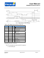
1 General description ................................................................................................... 7
2 Hardware .................................................................................................................... 8
3 Software.................................................................................................................... 11
4 System requirements .............................................................................................. 12
5 Installation EVB90609 software .............................................................................. 13
6 Technical Support.................................................................................................... 17
7 Contents ................................................................................................................... 18
7.1 Contents ............................................................................................................................................18
7.2 Menu Commands ..............................................................................................................................18
7.3 File Menu ...........................................................................................................................................18
7.4 View Menu .........................................................................................................................................19
7.5 Run Menu ..........................................................................................................................................19
7.6 Options Menu ....................................................................................................................................19
7.7 Help Menu .........................................................................................................................................20
8 Main Window ............................................................................................................ 21
8.1 Application menu ...............................................................................................................................21
8.2 Application’s toolbar ..........................................................................................................................21
8.3 Multifunctional status bar...................................................................................................................21
8.4 Pages.................................................................................................................................................22
9 Pages on main window ........................................................................................... 23
9.1 EEPROM Page..................................................................................................................................24
9.2 MODE Page.......................................................................................................................................26
9.3 SPI Page............................................................................................................................................29
9.4 ADC Page..........................................................................................................................................31
9.5 DEMO Page.......................................................................................................................................33
9.6 Run in DEMO MODE.........................................................................................................................35
10 Dialog windows...................................................................................................... 37
10.1 Dialog box - Open............................................................................................................................38
10.2 Dialog box - Save As… ...................................................................................................................39
EVB90609
Rev 1.01
Page 3 of 88
May-22
User Manual
EVB90609 Evaluation Board
10.3 Dialog box- Print preview.................................................................................................................43
10.4 Dialog box - Communication options...............................................................................................45
10.5 Dialog box - Demo options ..............................................................................................................46
10.5.1 Page Axis Y......................................................................................................................................................................47
10.5.2 Page Axis X......................................................................................................................................................................48
10.5.3 Page Series......................................................................................................................................................................49
10.5.4 Page Temperature ...........................................................................................................................................................50
10.5.5 Page Others .....................................................................................................................................................................51
10.6 Dialog boxes – Others .....................................................................................................................52
11 SPI Protocol............................................................................................................ 53
11.1 The refusal answer ..........................................................................................................................57
11.2 Instruction of the status reading (STATR) .......................................................................................57
11.3 Control mode instruction (MODEW) ................................................................................................58
11.4 Instruction of the ADC control (ADCC)............................................................................................58
11.5 Reading the EEPROM and the address setup (EER) .....................................................................58
11.6 Instruction of the data preparation (EED)........................................................................................59
11.7 Write instruction (EEW) ...................................................................................................................59
11.8 Instruction of a write/erase cancel (EEC) ........................................................................................59
11.9 Instruction of the ADC reading (ADCR)...........................................................................................59
11.10 Erasing the EEPROM contents .....................................................................................................61
11.11 Writing into the EEPROM: .............................................................................................................62
11.12 Finalizing the writing procedure.....................................................................................................63
12 EVB90609 Protocol ................................................................................................ 65
12.1 Timeouts ..........................................................................................................................................65
12.2 Commands ......................................................................................................................................66
12.2.1 A Command .....................................................................................................................................................................67
12.2.2 B Command .....................................................................................................................................................................70
12.2.3 C Command .....................................................................................................................................................................71
12.2.4 D Command .....................................................................................................................................................................73
12.2.5 W Commands...................................................................................................................................................................75
12.2.6 Z Command......................................................................................................................................................................77
12.2.7 Answer of the STAT .........................................................................................................................................................78
12.3 Checksum........................................................................................................................................79
13 Schematic ............................................................................................................... 80
EVB90609
Rev 1.01
Page 4 of 88
May-22
User Manual
EVB90609 Evaluation Board
14 Intel hex file format ................................................................................................ 82
14.1 Record Format.................................................................................................................................82
14.2 Data Records...................................................................................................................................83
14.3 Extended Linear Address Records (HEX386).................................................................................83
14.4 Extended Segment Address Records (HEX86) ..............................................................................84
14.5 End-of-File (EOF) Records..............................................................................................................85
14.6 Example Intel HEX File....................................................................................................................86
15 CSD format file ....................................................................................................... 87
16 Disclaimer............................................................................................................... 88
EVB90609
Rev 1.01
Page 5 of 88
May-22
User Manual
EVB90609 Evaluation Board
GLOSSARY OF TERMS
ADC – Analog-to-Digital Converter;
BMP – Bit Map;
BW – Bandwidth;
EVB – Evaluation Board;
EEPROM – Electrically Erasable Programmable Read-Only Memory;
GHz – Giga Hertz;
JPEG – Joint Photography Experts Group;
IBM PC – International Business Machines Personal Computer;
MB – Megabyte;
MHz – Mega Hertz;
OEM – Original Equipment Manufacture;
OUTAR – Output voltage of Angular Rate;
OUTTEMP – Output voltage of Temperature;
PCB – Printed Circuit Board;
RAM – Random-Access Memory;
R&D – Research and Development;
SPI – Serial Peripheral Interface;
SVGA – Super Video Graphics Array;
VCP – Virtual Communication Port;
VREF – Voltage Reference;
USB – Universal Serial Bus.
EVB90609
Rev 1.01
Page 6 of 88
May-22
User Manual
EVB90609 Evaluation Board
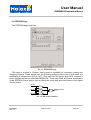
1 General description
The EVB90609 Evaluation Board is designed to support the MLX90609 family of
Angular Rate Sensor ICs. This board which acts as an interface between the USB port of a
PC and the MLX90609 can work in the following modes:
1. Digital mode (SPI only Interface);
2. Analog mode (only OUTAR, OUTTEMP, VREF, SELFTEST and ERROR pins);
3. Mixed mode (digital and analog mode);
4. Demo mode (direction indicator).
When the EVB90609 is used as a demo board, it works as a direction indicator (i.e. a
compass).
Power for the MLX90609 and EVB come from the computer USB port or from an
additional power supply (range from 4.75V up to 5.25V).
The EVB90609 is designed to allow customers to quickly configure the MLX90609
family of Angular Rate Sensor ICs. Customers can quickly experiment with temperature
ranges, power supply, EEPROM settings, etc.
The kit contains:
•
Main board;
•
USB cable to connect to a PC;
•
Sample MLX90609;
•
Software (EVB90609 Software, VCP driver) and documentation.
EVB90609
Rev 1.01
Page 7 of 88
May-22
User Manual
EVB90609 Evaluation Board
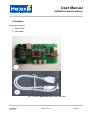
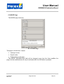
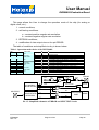
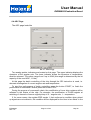
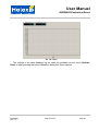
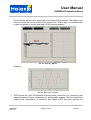
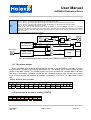
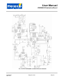
2 Hardware
Hardware contains:
1. Main board;
2. USB cable.
1
2
Pic. 1. The EVB90609 Hardware and USB cable.
EVB90609
Rev 1.01
Page 8 of 88
May-22
User Manual
EVB90609 Evaluation Board
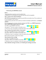
USB
USB B
Connector
J10
U9
USB Data
U8
RxD
USB to
RS-232
converter
TxD
RxD
Digital
Isolator
TxD
VDD1
U5
About 5 V
VDD1
U3
USB
POWER_EXT
J12
Voltage
regulator
J11
3.3 V
SCLK
VREF
MISO
OUTTEMP
MOSI
OUTAR
NSS
Cygnal
Microcontroller
ERROR
R6
FLT
J5
J4
C7
“Compass” data
J1
3.3 V
Power
External
J13
Compass
Connector
POWER_EXT
Pic. 2. Main board block diagram.
The board’s schematic is shown in the section Schematic.
Type of power supply source:
1. USB port;
2. Additional power supply (range from 4.75V up to 5.25V).
USB port
EVB90609
Rev 1.01
Power supply source
Additional power supply
Page 9 of 88
J6
J7
C10
SELFTEST
R5
From 4.75 V up to 5.25 V
MLX90609
J8
May-22
User Manual
EVB90609 Evaluation Board
Bandwidth:
The EVB90609 is designed to allow customers to quickly configure bandwidth of the
MLX90609. Customers can quickly experiment with the value of the bandwidth.
Procedure to change the bandwidth: you have to disconnect the bandwidth jumper with
a Filter label. After that you must put a capacitor into the collet socket.
Capacitor 82nF
Settings bandwidth
Additional capacitor
Bandwidth calculation: BW = 1/(2*π*R*C), Hz.
π = 3.1415926; R = 200 kOm; C – value of capacitor capacity.
For example:
π = 3.1415926; R = 200 kOm, C = 82nF.
BW = 1/(2*π*200000*82E-09) = 9.7 Hz.
EVB90609
Rev 1.01
Page 10 of 88
May-22
User Manual
EVB90609 Evaluation Board
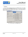
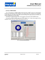
3 Software
The picture below shows the main window of the EVB90609 software. This software
uses its own protocol (see EVB90609 Protocol) for the connection with the main board
and controls the MLX90609 via SPI and/or SELFTEST pin. This software supports all
modes of operation of the MLX90609 (analog, digital and mixed mode) and has an
additional function: the demo mode.
Pic. 3. The main window of the EVB90609 software.
EVB90609
Rev 1.01
Page 11 of 88
May-22
User Manual
EVB90609 Evaluation Board
4 System requirements
The minimum requirements (not guarantied by Melexis):
1. IBM PC (or 100-percent compatible) machine with 16 Mb RAM;
2. SVGA Video Adapter;
3. Hard Disk Drive (3 Mb free space; with driver and documentation);
4. USB Port;
5. Mouse or Pointing Device;
6. Microsoft Windows 95/98/NT/2000/XP.
The recommended requirements:
1. IBM PC (or 100-percent compatible) machine 1 GHz with 512 MB RAM;
2. SVGA Video Adapter (Screen resolution 1024 by 768 pixels; Color quality: Highest
(32 bits));
3. Hard Disk Drive (3 Mb free space; with driver and documentation);
4. USB Port;
5. Mouse or Pointing Device;
6. Microsoft Windows XP.
EVB90609
Rev 1.01
Page 12 of 88
May-22
User Manual
EVB90609 Evaluation Board
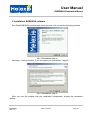
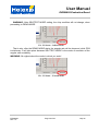
5 Installation EVB90609 software
Run SetupEVB90609.exe and wait some seconds until you see the following window
Pic. 4. Installation, Step 1.
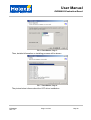
Next step - License window. If you are agree you must select “I agree”.
Pic. 5. Installation, Step 2.
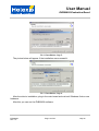
After you see the window with the installation components, choose the necessary
options.
EVB90609
Rev 1.01
Page 13 of 88
May-22
User Manual
EVB90609 Evaluation Board
Pic. 6. Installation, Step 3.
Then, detailed information on installing process will be shown.
Pic. 7. Installation, Step 4.
The picture below informs about the VCP driver installation.
EVB90609
Rev 1.01
Page 14 of 88
May-22
User Manual
EVB90609 Evaluation Board
Pic. 8. Installation, Step 5.
The picture below will appear if the installation was successful.
Pic. 9. Installation, Step 6.
After the driver’s installation, plug-in the main board and wait until Windows finds a new
hardware.
After this you can run the EVB90609 software.
EVB90609
Rev 1.01
Page 15 of 88
May-22
User Manual
EVB90609 Evaluation Board
Pic. 10. Installation, Step 7.
EVB90609
Rev 1.01
Page 16 of 88
May-22
User Manual
EVB90609 Evaluation Board
6 Technical Support
If you experience any problems with the module, Evaluation board or Software tools
please contact technical support. Specialized support can be reached through your local
sales representative.
EVB90609
Rev 1.01
Page 17 of 88
May-22
User Manual
EVB90609 Evaluation Board
7 Contents
7.1 Contents
Menu Commands
Main Window and Pages
Dialog Boxes
7.2 Menu Commands
File menu
View
Run
Options
Help
7.3 File Menu
The File menu offers the following commands:
Open
Save As…
Load internal EEPROM dump with the contents of selected file.
(Only User’s area).
Stores the contents of the EEPROM dump (all modes) and
Text format file, Excel format file, CSD Data file (OrCAD),
Bitmap format file, JPEG format file (Demo mode).
Print
Prints the graph of angular rate or/and temperature
(Demo mode).
Exit
EVB90609
Rev 1.01
Exits the EVB90609 software.
Page 18 of 88
May-22
User Manual
EVB90609 Evaluation Board
7.4 View Menu
The View menu offers the following commands:
Tool bar
Shows/hides Tool bar.
Status bar
Shows/hides Status bar.
Always on Top
Sets/resets always on top mode.
EEPROM
Shows EEPROM page.
MODE
Shows MODE page.
SPI
Shows SPI page.
ADC
Shows ADC page.
DEMO
Shows DEMO page.
7.5 Run Menu
The Run menu offers the following commands:
Connect/Disconnect
Connects/Disconnects to the EVB90609.
7.6 Options Menu
The Options menu offers the following commands:
Communication
Displays dialog window. Sets communication channel.
Demo
Displays dialog window. Sets demo mode (graph, angular rate
fitting).
EVB90609
Rev 1.01
Page 19 of 88
May-22
User Manual
EVB90609 Evaluation Board
7.7 Help Menu
The Help menu offers the following commands:
Content
Displays the Help Contents.
About…
Displays the version number and
Copyright information of the EVB90609 software.
EVB90609
Rev 1.01
Page 20 of 88
May-22
User Manual
EVB90609 Evaluation Board
8 Main Window
This is the main window application and it features the following settings:
8.1 Application menu
Complete list of the EVB90609 menu commands see Menu commands.
8.2 Application’s toolbar
The toolbar duplicates some of the commonly used menu commands:
Click
To execute
Connection/disconnection to the main board
The content help
8.3 Multifunctional status bar
The EVB90609 status bar is divided into 4 areas. The first area is used to display
application messages, 3 extra areas are provided for user convenience. The meaning of
each extra area follows:
•
Configuration of VCP – displays the configuration of virtual communication port
(number of port, bits per second, data bits, parity, stop bits);
•
Status of connection – displays the status of connection (connect\disconnect);
•
Mode of the chip – displays chip operating mode.
Note: closing the main window will close the application and the communication port .
EVB90609
Rev 1.01
Page 21 of 88
May-22
User Manual
EVB90609 Evaluation Board
8.4 Pages
The main window has 5 pages:
Pic. 11. Main window pages.
EVB90609
Rev 1.01
Page 22 of 88
May-22
User Manual
EVB90609 Evaluation Board
9 Pages on main window
Pages are divided into the following sections:
•
EEPROM;
•
MODE;
•
SPI;
•
ADC;
•
DEMO.
EVB90609
Rev 1.01
Page 23 of 88
May-22
User Manual
EVB90609 Evaluation Board
9.1 EEPROM Page
The EEPROM page looks like
Pic. 12. EEPROM Page.
This page is divided in 2 banks: User’s space is available for recording, erasing and
changing contents. These banks have the following characteristics: each is of 8 bytes; the
addressing is ranged from 0x70 to 0x7F. Zero bank has its specific byte 0x70, in which 3
minor changes are the so called bits MEMLOCK. These bits forbid any further modification
of the EEPROM User’s space, they are bit-by-bit voting and work like shown in the logical
circuitry below:
Bit #0
Bit #1
MEMLOCK bit
Bit #2
Pic. 13. Bit-by-bit violation.
EVB90609
Rev 1.01
Page 24 of 88
May-22
User Manual
EVB90609 Evaluation Board
This page provides the below functionalities:
1. Recording to EEPROM (recording only to bank 0, recording only to bank 1, and
recording to both banks). For convenience, the recording fields are located in the same
sequence as in dump of memory; the space for byte #70 was specially eliminated. This
byte contains 3 bit-by-bit voting bits.
Warning! Setting at least 2 bits to “1” disables any further modification of the User’s
memory EEPROM. This setting comes into effect only after switching off the supply.
If you have disabled the User’s memory space by accident and then need to reset the
User’s memory EEPROM, please contact Melexis.
The data input to the fields of recording is done in hex format, which is equivalent to
ASCII format. For example, digits ‘0’ – 0x30; ‘9’ – 0x39, and letters ‘A’ – 0x41 and ‘a’ –
0x61. Digits input have to be done without prefix.
For example, input of line “Melexis”. We need to input the following hex digits: 4D, 65,
6C, 65, 78, 69 and 73.
2. EEPROM erasing. You can erase the EEPROM as separate banks, as well as the
whole User’s space. For this you can use the button Erase in the applicable areas, or the
button Erase all.
3. EEPROM reading. After pressing the button Read, the program will read the data
from the User’s space. The technical data can not be modified by the User. The technical
data is read only when the software is connected to the EVB90609.
After each EEPROM data manipulation, a verification of the recorded (rerecorded,
deleted) data takes place by a repeated reading of the EEPROM User’s space.
EVB90609
Rev 1.01
Page 25 of 88
May-22
User Manual
EVB90609 Evaluation Board
9.2 MODE Page
The MODE page looks like
Pic. 14. Mode Page.
This page is divided into 3 areas:
•
Analogue mode;
•
Digital mode;
•
Explanations to the User.
The MODE INFORMATION field will be changed every time the User modifies the
page, but the modifications will only be activated after the OK button is pressed.
EVB90609
Rev 1.01
Page 26 of 88
May-22
User Manual
EVB90609 Evaluation Board
This page allows the User to change the operation mode of the chip (for analog or
digital mode, etc.):
1. normal conditions;
2. self-testing conditions:
a. constant positive angular rate emulation
b. constant negative angular rate emulation
3. EEPROM conditions;
4. modification of data output view on the pin ERROR.
The table of conditions and simplified circuitry is shown below:
Table 1. Operation mode choice of the MLX90609.
SPI
SFT1
0
0
1
1
0
0
1
1
0
0
1
1
SFT0
0
1
0
1
0
1
0
1
0
1
0
1
SELFTEST
pin
5.0 Volt,
Out Code:
00
2.5 Volt,
Out Code:
10
0.0 Volt,
Out Code:
01
SF[1:0]
EEDIS
MODE name
00
01
10
11
10
11
10
11
01
01
11
11
1
1
1
0
1
1
1
0
1
1
1
0
Normal mode
SELFTEST mode, emulation of the POSITIVE angular rate
SELFTEST mode, emulation of the NEGATIVE angular rate
EEPROM mode with INTERNAL charge pump
SELFTEST mode, emulation of the NEGATIVE angular rate.
Not used combination
SELFTEST mode, emulation of the NEGATIVE angular rate
EEPROM mode with INTERNAL charge pump
SELFTEST mode, emulation of the POSITIVE angular rate
SELFTEST mode, emulation of the POSITIVE angular rate
Not used combination
EEPROM mode with INTERNAL charge pump
ERRP
ECRC
ERR
EOC
SPI “MODEW” INSTRUCTION
OR2
ERRS
SFT1
SFT0
OR2
NAND2
OR2
SELFTEST
THREE STATE
DETECTOR
OR2
DMUX2-1
IN0
IN1
SEL
XOR2
HIGH VOLTAGE
ERROR
EEPROM
EDIS
SF0
SF1
EXCITATION
MEMS
PART
Pic. 15. Simplified schematic of ERROR and SELFTEST circuit.
EVB90609
Rev 1.01
Page 27 of 88
May-22
User Manual
EVB90609 Evaluation Board
REMARKS:
1. The table and the figures above were composed to explain all possible sub-modes
related to the SELFTEST pin and SFT-bits.
2. Bits SFT [1:0] is cleared after power-up.
3. STATUS OF THE CHIP explains the value of the internal bits (without taking state of
the SELFTEST pin), the ERROR pin and the value of the SELFTEST pin. Field
MODE INFORMATION displays comments with taking into account the state of the
SELFTEST pin.
4. Each modification will display into the Status of the chip.
EVB90609
Rev 1.01
Page 28 of 88
May-22
User Manual
EVB90609 Evaluation Board
9.3 SPI Page
The SPI page looks like
Pic. 16. SPI Page.
On this page the User has the possibility to work with a low-level SPI instruction. Please
find a more detailed description of the SPI instructions in the section SPI instruction. (see
SPI protocol).
This page is divided into 4 fields:
The 1st field represents the SPI instruction (8 bits) and data (16 bits).
The 2nd field represents the answer for an earlier sent SPI instruction (the detailed
description of the SPI instruction answers can be found in the section SPI protocol).
The 3rd and 4th fields are information areas. The 3rd field explains specified SPI
instruction, and the 4th gives a detailed description of the answer to a sent SPI instruction.
EVB90609
Rev 1.01
Page 29 of 88
May-22
User Manual
EVB90609 Evaluation Board
REMARKS:
1. SPI COMMAND INFORMATION explains the specified SPI instruction by taking
state of the SELFTEST pin (the value of the supply is displayed into parenthesis).
2. Each modification will be displayed in the Status of the chip.
EVB90609
Rev 1.01
Page 30 of 88
May-22
User Manual
EVB90609 Evaluation Board
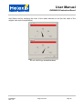
9.4 ADC Page
The ADC page looks like
Pic. 17. ADC Page.
Two analog pointer indicators are located on this page. The upper indicator displays the
dynamics of the angular rate. The lower indicator shows the dynamics of temperaturesensitive element. The values range from 0 up to 2048 (this range is determined by the bit
capacity of the used ADC, 11 bits).
At this page the batch controlling of the chip through the SPI Instruction is used, i.e.
alternate interrogation of current angular rate and temperature.
To start the performance of batch controlling press the button START, to finish the
performance of command’s chains press the button STOP.
During the process of command’s chain, the modification of inner chip registers will be
reflected in the Status of the chip. For example, the modification of CHAN register at
switching of channels of source signal pickup is 0 – angular rate, 1 – temperature.
If, for some reason, the register ERR equals 1, that conforms to condition when picked
up signals are not authentic, this condition will be displayed for the User in two fields: in the
EVB90609
Rev 1.01
Page 31 of 88
May-22
User Manual
EVB90609 Evaluation Board
chip Status and by changing the color of the index indicator to red (for the value of the
angular rate and/or temperature).
Pic. 18. ADC Page (anomalous data).
EVB90609
Rev 1.01
Page 32 of 88
May-22
User Manual
EVB90609 Evaluation Board
9.5 DEMO Page
The DEMO page looks like
Pic. 19. DEMO Page.
This page contains 3 fields: a page like an analog compass indicator, an analog
thermometer indicator and a table of read values (the table contains the data about the
measurement time intervals, the values of the angular rate and temperature). The
temperature value can be shown in different units (see Dialog box – Demo Options):
ADC code, Celsius, Fahrenheit and Kelvin degree.
While opening this page, the content of the EEPROM and the Status of the chip will be
hidden. The chart of angular rate modification and/or temperature will be shown instead.
Two digital indicators showing the current angular rate and temperature are located over
the chart.
EVB90609
Rev 1.01
Page 33 of 88
May-22
User Manual
EVB90609 Evaluation Board
Pic. 20. Chart.
The settings of the data displayed on the chart are available via text menu OptionsDemo or after pressing the buttons Ctrl+D in dialog box Demo options.
EVB90609
Rev 1.01
Page 34 of 88
May-22
User Manual
EVB90609 Evaluation Board
9.6 Run in DEMO MODE
To run the program in DEMO MODE press the button START. During an interchanging
between the main board and the software, the coming data will be shown on the indicators,
on the chart and in the table. While data communicating other pages will be unavailable, as
well as modifications of chip modes.
To specify or install the zero value of the angular rate press the SET ZERO button.
To stop the DEMO MODE press the STOP button, as a result other pages will be
available, and the process of data interchange will be over.
Pic. 21. Demo mode operation.
EVB90609
Rev 1.01
Page 35 of 88
May-22
User Manual
EVB90609 Evaluation Board
WARNING: After SELFTEST MODE setting, the chip condition will not change, when
proceeding to DEMO MODE.
Pic. 22. Status – Selftest mode.
That is why, after the DEMO MODE starts, the angular rate will be observed, while PCB
is stationary. It will take place because SELFTEST MODE is the mode of emulation of the
angular rate availability.
WARNING: Be vigilant about the mode in which you work!
Pic. 23. Status – Normal mode.
EVB90609
Rev 1.01
Page 36 of 88
May-22
User Manual
EVB90609 Evaluation Board
10 Dialog windows
The EVB90609 software has the following dialog boxes:
•
Open;
•
Save As;
•
Print preview;
•
Communication options;
•
Demo options;
•
Others.
EVB90609
Rev 1.01
Page 37 of 88
May-22
User Manual
EVB90609 Evaluation Board
10.1 Dialog box - Open
This standard dialog box of file opening can be reached through the text menu FileOpen or the buttons Ctrl+O.
This dialog box allows opening files in HEX format. These files are the dump of the chip
EEPROM chip that were saved before by this program (see Dialog box Save as…).
Following the file opening, the fields of inputting will be filled with EEPROM byte over the
range of 0x70 up to 0x7F by the file data. Further these data could be written to the
EEPROM of a new chip.
EVB90609
Rev 1.01
Page 38 of 88
May-22
User Manual
EVB90609 Evaluation Board
10.2 Dialog box - Save As…
This standard dialog box of file saving can be reached through text menu File-Save
as… or buttons Ctrl+S.
This dialog box allows to store the contents dump of the EEPROM chip in HEX format
file (see Intel Hex file format) (all modes) and Text format file, Excel format file, CSD
format file – OrCAD (see CSD format file), Bitmap format file, JPEG format file (Demo
mode).
All contents of EEPROM are stored in HEX mode in address space from 0x0000 to
0x007F. This mode is described in section Intel HEX file format (see Intel HEX file
format).
You can store the received data of the angular rate, temperature and time intervals in
DEMO MODE as well. The data can be in the following modes:
•
Text format file. Delimiter is space. For example:
Date:<space><current date>
Time:<space><current time>
Time(sec)<space>Angular_rate(°/sec)<space>Temperature(ADC_code)
0.000000E+00<space>6.200000E+01<space>1.311000E+03
3.250000E-01<space>6.200000E+01<space>1.311000E+03
3.500000E-01<space>4.000000E+00<space>1.310000E+03
•
Excel format file. It’s text file with delimiter of tab. For example:
Date:<tab><current date>
Time:<tab><current time>
Time(sec)<tab>Angular_rate(°/sec)<tab>Temperature(ADC_code)
0.000000E+00<tab>6.200000E+01<tab>1.311000E+03
3.250000E-01<tab>6.200000E+01<tab>1.311000E+03
EVB90609
Rev 1.01
Page 39 of 88
May-22
User Manual
EVB90609 Evaluation Board
•
CSD format file. More detail information look at section of CSD format file. Example:
#H
SOURCE='PSPICE' VERSION='PSpice 9.2 (Mar 2000)'
TITLE='* Measurement *'
SUBTITLE='Angular rate'
TIME='<current time>' DATE='<current date>' TEMPERATURE='var'
ANALYSIS='Transient Analysis' SERIALNO='61414'
ALLVALUES='NO' COMPLEXVALUES='NO' NODES='2'
SWEEPVAR='Time' SWEEPMODE='VAR_STEP'
XBEGIN='0.000000E+00' XEND='1.804000E+00'
FORMAT='0 VOLTSorAMPS;EFLOAT : NODEorBRANCH;NODE '
DGTLDATA='NO'
#N
'Angular_rate(°/sec)' 'Temperature(ADC_code)'
#C 0.000000E+00 2
6.200000E+01:1 1.311000E+03:2
#C 3.250000E-01 2
6.200000E+01:1 1.311000E+03:2
#C 3.500000E-01 2
4.000000E+00:1 1.310000E+03:2
#C 1.804000E+00 2
0.000000E+00:1 1.311000E+03:2
#;
•
Bitmap format file. This file format is the MS-Windows standard format. It holds
truecolor images. Note there is also an OS/2-BMP format. All values stored in the
BMP file are in the Intel format, sometimes also called the little endian format
because of the byte order that an Intel processor uses internally to store values.
EVB90609
Rev 1.01
Page 40 of 88
May-22
User Manual
EVB90609 Evaluation Board
The saved file will store the shown info in the chart of main window. The bigger is the
chart the better will be the quality of the graphics file. That is why it is recommended
to take the splitter by mouse and drag it to the leftmost position.
Pic. 24. Moving splitter.
Example:
Pic. 25. Best view of chart.
•
JPEG format file (Joint Photographic Experts Group) format file is a commonly used
standard method of lossy compression for photographic images. The file format which
employs this compression is commonly also called JPEG; the most common file
EVB90609
Rev 1.01
Page 41 of 88
May-22
User Manual
EVB90609 Evaluation Board
extensions for this format are .jpeg, .jfif, .jpg. JPG or JPE although is the most
common on all platforms.
The recommendations regarding the image quality improvement is the same as for
bitmap format files.
The JPEG settings are at default:
•
Save compression quality = 90%;
•
Progressive encoding = true.
These settings allow getting the best indices ratio file size/image quality.
Example:
Pic. 26. Temperature chart.
EVB90609
Rev 1.01
Page 42 of 88
May-22
User Manual
EVB90609 Evaluation Board
10.3 Dialog box- Print preview
This dialog box of printing can be reached through text menu File-Print-Preview or
buttons Ctrl+P.
This dialog box allows printing only chart (the chart that is shown in the right part of the
main window – DEMO MODE). To get the image of the best quality move the splitter on
the main window to the leftmost position. After that, call the dialog window by one of
possible ways.
This dialog box is a combination of the following spaces:
•
Printer setup (Printer, Printer setup and others);
•
Page orientation (portrait, landscape);
•
Margins(% values, reset margins, view margin);
•
Detail (from normal up to more);
•
Proportional option (default uncheck).
To increase grid's refining on the chart move the slider Details to the position More.
Pic. 27. Print preview.
EVB90609
Rev 1.01
Page 43 of 88
May-22
User Manual
EVB90609 Evaluation Board
If required to make a PDF file of an existing chart it is recommended to use the program
PDFCreator. PDFCreator is a freeware software. It easily creates a PDF of the EVB90609
program. For more information and file download, enter
http://sourceforge.net/projects/pdfcreator/.
EVB90609
Rev 1.01
Page 44 of 88
May-22
User Manual
EVB90609 Evaluation Board
10.4 Dialog box - Communication options...
This is a dialog box of the communication path settings between the EVB90609
software and the EVB90609 PCB and it is called through the text menu File-OptionsCommunication or by the buttons Ctrl+C.
This dialog box is called automatically during the first start and later on when it is
required to modify the communication port to the EVB90609 PCB. If it is required to modify
the communication port to the EVB90609 the procedure of disconnecting has to be done,
i.e. choose the text menu Port-Disconnect or press F5, or switch the tumbler to the
position Disconnect.
Pic. 28. Setting switch in position disconnect.
The dialog box looks like:
Pic. 29. Dialog box – Communication options.
The dialog box contains the following parts:
Dependent list in which the available ports are shown.
The button of ports’ lists update. This button is essential as the EVB90609 PCB is a
plug-and-play device working through USB port, and as a result the operating system
needs some time to reveal and register the device in the system. And it happens
sometimes that there are no necessary VCP in the list.
Checkbox that points the program to connect automatically to the
EVB9069 PCB.
REMARK: The settings of the data are to be performed only after pressing the OK
button.
EVB90609
Rev 1.01
Page 45 of 88
May-22
User Manual
EVB90609 Evaluation Board
10.5 Dialog box - Demo options
This dialog box of the demo mode settings can be reached through the text menu FileOptions-Demo or by the buttons Ctrl+D.
This window looks like:
Pic. 30. Demo options – main view.
This dialog box has 5 pages:
•
Axis X;
•
Axis Y;
•
Series;
•
Temperature;
•
Other.
EVB90609
Rev 1.01
Page 46 of 88
May-22
User Manual
EVB90609 Evaluation Board
10.5.1 Page Axis Y
There are settings of data display on Axis Y at this page. There are 3 operation modes:
Automatic, automatically scaling at axis Y (from minimum up to maximum value);
Automatic (data from chip), range is read out from the EEPROM of the chip (range
equals from (-range-10) up to (range+10));
Manual, manual control – settings appointed to the User. For example, a range from
1000 up to 1400.
Pic. 31. Demo options – Y Axis Page.
EVB90609
Rev 1.01
Page 47 of 88
May-22
User Manual
EVB90609 Evaluation Board
10.5.2 Page Axis X
On this page the User sets the quantity of the displayed data on axis X in a range from
10 up to 9999999.
Pic. 32. Demo options – X Axis Page.
EVB90609
Rev 1.01
Page 48 of 88
May-22
User Manual
EVB90609 Evaluation Board
10.5.3 Page Series
On this page the User sets the quantity of the displayed series (data for displayed on
the chart). Setting (cleaning) of a tick makes seen (invisible) to a series on the chart.
Pic. 33. Demo options – Series Page.
EVB90609
Rev 1.01
Page 49 of 88
May-22
User Manual
EVB90609 Evaluation Board
10.5.4 Page Temperature
The following variants are possible:
•
ADC code;
•
Celsius degrees;
•
Fahrenheit degrees;
•
Calvin degrees.
Display of the temperature data in terms of the ADC code is established by default.
The quantity of probable variants of data shown depends on the chip type.
Pic. 34. Demo options – Temperature Page.
EVB90609
Rev 1.01
Page 50 of 88
May-22
User Manual
EVB90609 Evaluation Board
10.5.5 Page Others
At this page there is a setting of scale size factor fitting and value of angular rate data
averaging.
For the specification of the directional indicator display ("compass"), it is necessary to
enter the correction factor into the field Scale Factor Fitting.
Calculation procedure of the correction factor:
1. If the demo mode is running, stop it by pressing on the STOP button;
2. Install the value of the Scale Factor Fitting to “1”;
3. Turn a PCB on the valid 360 degrees;
4. Then, the value of the indicator "compass" is to be divided by 360; for example, if
the value on the indicator is 300: 300/360 = 0.833333;
5. The obtained number has to be entered into a field of Scale Factor Fitting (look at
Pic. 35.).
Pic. 35. Demo options – Others Page.
EVB90609
Rev 1.01
Page 51 of 88
May-22
User Manual
EVB90609 Evaluation Board
10.6 Dialog boxes – Others
Other dialog boxes are warning and error messages. These messages are shown
during running of the application when there is not a typical situation originating on fault of
the user or other programs (for example, an operational system).
For example, this message will appear when the user sets an incorrect data about the
number of the port. The application will try to connect to the main board, but will not receive
the answer in the set time interval. It will be a timeout error.
Pic. 36. Demo options – Others Pages.
EVB90609
Rev 1.01
Page 52 of 88
May-22
User Manual
EVB90609 Evaluation Board
11 SPI Protocol
The MLX90609 has a serial communication interface compatible with SPI. Likewise SPI the
Serial Interface of the MLX90609 specifies four signals:
•
•
•
•
serial clock (SCLK);
master data output, slave data input (MOSI);
master data input, slave data output (MISO); and
slave select ( SS ).
The MLX90609 always operates as a slave. Therefore only MISO pin is an output.
The MLX90609 is selected when the SS pin is low (see Fig. 37.). When SS pin is high, data
will not be accepted via the MOSI pin. The serial output pin (MISO) will remain in a high impedance
state. High level of SS forces the serial interface into the start state of data exchange.
Data is serially transmitted to the MLX90609 in 8 bit words (a command byte) and in 16 bit data
words. Data is serially received from the MLX90609 in 16 bit words (an answer word). Most
Significant Bit (MSB) is the first bit transmitted and received.
Transmission:
After the device is selected with SS going low, the command byte will be received by the
MLX90609. On each rising edge of SCLK data from MOSI enter into an internal 8-bit shift register.
The accepted command byte contains the op-code that defines the operations to be performed.
Along with op-code this byte can also contain information such as EEPROM address or ADC mode
(to be setup). One of the commands (see Instruction of the data preparation (EED)) also needs
16 bit data word transmission which should be shifted to the MLX90609 together with reception
answer.
Reception:
After the 8th bit is received to the shift register, the command will be executed by the
MLX90609. The format of the outgoing data is defined by the received command. All commands
evoke an answer. A full communication cycle (transmitting a command and receiving the full
answer) is finished after 24th clock of the SCLK. Communication can be terminated by putting SS
high.
Some remarks:
•
•
•
If an invalid op-code is received, it is rejected and the corresponding data is ignored. In this
case a special refusal answer will be generated.
It's recommended to use synchronization by SS after every data exchange to prevent a
data distortion.
If high level is applied to SS during a command byte transmission, the command will be
ignored.
EVB90609
Rev 1.01
Page 53 of 88
May-22
User Manual
EVB90609 Evaluation Board
•
If high level SS is applied during the answer reception, the answer will be truncated. This
can be used to limit the reading of the answer to e.g. one byte only (see Fig. 38.).
Pic. 37. Serial Exchange Sequence (full answer reading).
Pic. 38. Serial Exchange Sequence (the reading of the higher half of the answer).
EVB90609
Rev 1.01
Page 54 of 88
May-22
User Manual
EVB90609 Evaluation Board
Pic. 39. Synchronous Data Timing.
Table 2. SPI Timing Characteristics (see Fig. 38).
Parameter
Limit
Units
Test Conditions/Comments
t1
Minimum 30
ns
SS
t2
Minimum 80
ns
SCLK High Duration
t3
Minimum 80
ns
SCLK Low Duration
t4
Minimum 0
ns
SS
Hold Time
t5
Minimum 50
ns
SS
High Duration
t6
Minimum 80
ns
Data In Setup Time
T7
Minimum 50
ns
Data In Hold Time
T8
Maximum 50
ns
Output Valid
T9
Minimum 0
ns
Output Hold Time
T10
Maximum 40
ns
Output Disable Time
to SCLK Rising Edge Setup Time
MLX90609 commands and answers
The SPI commands are mainly used for 3 purposes:
•
EVB90609
Rev 1.01
for the status poll
Page 55 of 88
May-22
User Manual
EVB90609 Evaluation Board
•
for the EEPROM manipulation: reading the EEPROM contents or writing/erasing
the customers banks
•
for the internal ADC control: reading the 11 bit angular rate or temperature
output.
Table 3 gives the description of each command and answer bit.
Table 3 It has to be named: e.g. “SPI bits description” or somehow else.
OPC
EOC
MLB
EEB
BUSY
EEDIS
Reserved
ECRC
EDRV,
EPLL
and
ERR
BN
ERRP,
ERRS
SF1, SF0
CHAN
ADEN
ADCM1,
ADCM0
EVB90609
Rev 1.01
Unknown Operation Code.
This bit is set when a received operation code was not recognized.
End of AD-conversion bit. EOC bit indicates an ADC state.
EOC=0 : ADC in progress and can not be restarted.
EOC=1 : AD-conversion has been completed and can be restarted.
As a result, any attempt of the ADC starting will be rejected if EOC has a “0” state.
When this bit is set to “1”, the EEPROM is not available anymore for writing or erasing.
EEPROM busy bit. Being set this bit informs that the EEPROM is in a busy state and that no operation (writing/erasing or
reading) can be performed on it.
This bit will be set after a reset and will be toggled to zero after all initialization procedures inside the MLX90609. While
BUSY=1, only refusal answers will be sent.
EEDIS = (SFT1 NAND SFT0). This bit informs that the internal chip high voltage is being used to drive the MEMS and is
not available for erasing or writing into the EEPROM.
These bits are reserved and have an undefined state.
CRC Error indicator. An incorrect result of the CRC calculation will set ECRC to “1”. In this case, a refusal answer will
always be generated and the ERROR pin will keep a high logical state. toggle to the selected error logical state (with the
command bit ERRP).
EDRV and EPLL bits reflect the result of the Continuous Self Test which is used to monitor and detect
permanent/temporary errors in the primary mode amplitude (EDRV) and frequency of oscillations (EPLL). After the status
reading bits EDRV and EPLL will be cleared by hardware. To clear EDRV and EPLL bits it’s possible also to apply zero
pulse to the SELFTEST pin. ERR bit combines EDRV, EPLL and ECRC bits by OR logic.
BN bit defines the number of the customer’s bank of the EEPROM to be erased or written (see EEE and EEW
instructions). This bit should be preloaded before any write/erase procedure by using EER instruction.
BN = 0 means EEPROM bank 70H…77H
BN = 1 means EEPROM bank 78H…7FH
These bits are set by the MODEW-instruction. The ERRS bit selects the source controlling the ERROR pin and the
ERRP bit defines the polarity of the ERROR pin:
ERRP=0, ERRS=0 : ERROR pin is controlled by the ERR and ECRC bits connected via an OR gate.
ERROR = ERR or ECRC
ERRP=0, ERRS=1 : ERROR pin is controlled by the ERR, ECRC and EOC bits.
ERROR = (ERR or ECRC) or EOC
ERRP=1, ERRS=0 : ERROR pin is controlled by the inverted result of (ERR or ECRC).
ERRP=1, ERRS=1 : ERROR pin is controlled by the bit not ((ERR or ECRC) or EOC).
The ERRP and ERRS bits are helpful for the fitting of the ERROR pin to the interruption input of the external
microprocessor.
After power-up bits ERRP and ERRS are cleared.
When the SELFTEST pin is in the high logical state, the bits SF1 and SF0 reflect the state of SFT1 and SFT0
respectively.
The CHAN bit is used to select the input source for the ADC.
CHAN=0: the angular rate channel.
CHAN=1: the temperature sensor channel.
This bit is set by the ADCC-instruction. After power-up bit CHAN is cleared.
The ADEN bit selects the power management mode of the ADC:
ADEN=0: ADC is switched to the sleep mode, no AD-conversion is allowed.
ADEN=1: AD-conversion is allowed.
This bit is set by the ADCC-instruction. After power-up bit ADEN is cleared.
These bits are used to choose an ADC operation mode:
ADCM1=0, ADCM0=0: AD-conversion is initiated by the ADCC-instruction.
The other combinations are reserved for future designs. If these bits are not cleared, CHAN and ADEN bits will be
loaded but the ADC will not start and a refusal answer will be generated.
Page 56 of 88
May-22
User Manual
EVB90609 Evaluation Board
This couple of bits are used to select between Self-Test mode and EEPROM mode.
SFT1=0, SFT0=0 : Normal operation (pin SELFTEST has high logical state)
SFT1=0, SFT0=1 : Self-Test mode (positive angular rate emulation; pin SELFTEST has high logical state)
SFT1=1, SFT0=0 : Self-Test mode (negative angular rate emulation; pin SELFTEST has high logical state)
SFT1=1, SFT0=1 : EEPROM programming / erasing
There are two ways to setup Self-Test mode for the MLX90609: by using the MODEW instruction or by managing
SELFTEST pin. To prevent interference it’s recommended to hold SELFTEST pin at the high logical state if the MODEW
instruction is used. On the other hand bits SFT1 and SFT0 have to be cleared before using the SELFTEST pin to setup a
Self-Test mode.
After power-up bits SFT1 and SFT0 are cleared.
SFT1,
SFT0
ERRP
ECRC
ERR
EOC
OR2
ERRS
SFT1
SFT0
SPI “MODEW” INSTRUCTION
DMUX2-1
IN0
IN1
SEL
OR2
ERROR
EEPROM
HIGH VOLTAGE
NAND2
EDIS
OR2
SF0
SELFTEST
THREE STATE
DETECTOR
XOR2
OR2
SF1
EXCITATION
MEMS
PART
Pic. 40. Simplified schematic around pins ERROR and SELFTEST.
11.1 The refusal answer
Every command sent to the MLX90609 has an answer. If the MLX90609 is not able to accept
the instruction a refusal answer will be transmitted out. This answer has a unique format which is
shown in the table 4 below. The refusal answer is the only one that has a settled MSB. The other
bits help to understand a possible reason for the command rejection. One can also on purpose
force a refusal answer (for example by sending a command “11111111b”) to read some of those
bits.
Table 4. Refusal answer format.
Bit
15
1
Bit
14
OPC
Bit
13
EOC
Bit
12
MLB
Bit
11
EEB
Bit
10
BUSY
Refusal answer
Bit
Bit
Bit
9
8
7
EEDIS Reserved
Bit
6
ECRC
Bit
5
EPLL
Bit
4
EDRV
Bit Bit Bit
3
2
1
Reserved
Bit
0
11.2 Instruction of the status reading (STATR)
Bit 7
1
Bit 6
0
EVB90609
Rev 1.01
Bit 5
0
Command
Bit 4 Bit 3
0
1
Bit 2
X
Bit 1
X
Bit 0
X
Page 57 of 88
May-22
User Manual
EVB90609 Evaluation Board
Table 5. Format of the STATR instruction.
Bit
15
0
Bit
14
ERR
Bit
13
EOC
Bit
12
MLB
Bit
11
EEB
Bit
10
BN
Bit
Bit
9
8
Reserved
Answer
Bit
7
ERRP
Bit
6
ERRS
Bit
5
SF1
Bit
4
SF0
Bit
3
CHAN
Bit
2
ADEN
Bit
Bit
1
0
Reserved
11.3 Control mode instruction (MODEW)
Table 6. Format of the MODEW instruction (The answer is the same as for the STATR
instruction).
Bit 7
1
Bit 6
0
Bit 5
1
Command
Bit 4 Bit 3
0
ERRP
Bit 2
ERRS
Bit 1
SFT1
Bit 0
SFT0
11.4 Instruction of the ADC control (ADCC)
Table 7. Format of the ADCC instruction (The answer is the same as for the STATR
instruction).
Bit 7
1
Bit 6
0
Bit 5
0
Bit 4
1
Command
Bit 3
Bit 2
CHAN ADEN
Bit 1
ADCM1
Bit 0
ADCM0
11.5 Reading the EEPROM and the address setup (EER)
Bit 7
0
Bit 6
A6
A6…A0
Bit 5
A5
Command
Bit 4 Bit 3
A4
A3 / BN
Bit 2
A2
Bit 1
A1
Bit 0
A0
Address of the EEPROM cells to be read or to write/erase.
For the read operation all of these bits are significant and result of the reading will be included into the answer.
The second result of the operation is a loading of the BN bit. This bit has to be preloaded before each write/erase operation as
it defines the number of the customer’s EEPROM bank to be erased or written (see EEE and EEW instructions). It’s also
recommended to setup bits A2…A0 to zero before write/erase procedure.
BN = 0 means EEPROM bank 70H…77H
BN = 1 means EEPROM bank 78H…7FH
After power-up the bits A6…A0 and BN are cleared.
Table 8. Format of the EER instruction.
Bit
15
0
Bit
14
ERR
Bit
13
EOC
EVB90609
Rev 1.01
Bit
12
MLB
Bit Bit Bit
11 10 9
Reserved
Bit
8
Answer
Bit
Bit
7
6
DR7 DR6
Bit
5
DR5
Bit
4
DR4
Page 58 of 88
Bit
3
DR3
Bit
2
DR2
Bit
1
DR1
Bit
0
DR0
May-22
User Manual
EVB90609 Evaluation Board
DR7…DR0
The result of the EEPROM reading.
Warning: At least 60 us delay should be guaranteed after the shifting of the command LSB and before the DR7 reading in
order to read a correct EEPROM data.
11.6 Instruction of the data preparation (EED)
Bit 7
1
Bit 6
0
Bit 5
0
Command
Bit 4 Bit 3
0
0
Bit 2
1
Bit 1
AW1
Bit 0
AW0
Table 9: Format of the EED instruction (The answer is the same as for the STATR
instruction).
AW1…AW0
A destination address of 16-bit data word in 64-bit data word to be written into the EEPROM. The 16-bit word should be
shifted after instruction during the answer receiving.
11.7 Write instruction (EEW)
Table 10: Format of the EEW instruction (The answer is the same as for the STATR
instruction).
Bit 7
1
Bit 6
0
Bit 5
0
Command
Bit 4 Bit 3
0
0
Bit 2
0
Bit 1
1
Bit 0
1
Note: BN bit defines the number of the customer’s bank of the EEPROM to be written. If BN=0
the cells 70H…77H will be written, otherwise if BN=1 the cells 78H…7FH will be written. Bit BN
should be specified previously by the EER-instruction as well as 64-bit data word should be
specified by the EED-instruction.
11.8 Instruction of a write/erase cancel (EEC)
Table 11: Format of the EEC instruction (The answer is the same as for the STATR
instruction).
Bit 7
1
Bit 6
0
Bit 5
0
Command
Bit 4 Bit 3
0
0
Bit 2
0
Bit 1
0
Bit 0
1
11.9 Instruction of the ADC reading (ADCR)
Bit 7
1
Bit 6
0
EVB90609
Rev 1.01
Bit 5
0
Command
Bit 4 Bit 3
0
0
Bit 2
0
Bit 1
0
Bit 0
0
Page 59 of 88
May-22
User Manual
EVB90609 Evaluation Board
Table 12: Format of the ADCR instruction
Bit
15
0
Bit
14
ERR
Bit
13
EOC
AD10…AD0
EVB90609
Rev 1.01
Bit
12
MLB
Bit
11
AD10
Bit
10
AD9
Bit
9
AD8
Answer
Bit
Bit
8
7
AD7 AD6
Bit
6
AD5
Bit
5
AD4
Bit
4
AD3
Bit
3
AD2
Bit
2
AD1
Bit
1
AD0
Bit
0
0
A result of the AD-conversion. These bits are valid only when EOC bit is set.
Page 60 of 88
May-22
User Manual
EVB90609 Evaluation Board
11.10 Erasing the EEPROM contents
Notes:
The bit with leftmost position should be shifted first.
If MEMLOCK bit is activated the erase/write procedure will be impossible.
Step 1 (setup of the initial conditions)
SELFTEST pin should be free or pulled up and HVIN pin should be free (This condition will
be not necessary for BA-version).
Internal booting procedure after power-up should be finalized (bit BUSY=0; see Refusal
answer).
Previous erase/write procedure should be finalized (bit EEB=0; see STATR instruction).
Step 2 (EEPROM programming mode setup)
Use SPI to send MODEW instruction:
1010xx11xxxxxxxxxxxxxxxx
And check 15th bit of the answer (it should be zero):
0xxxxxxxxxxxxxxx
If 15th bit isn’t zero it’s necessary to check the cause of the refusal answer.
Step 3 (setup of the bank number to be erased)
Use SPI to send EER instruction (check table 8):
And check 15th bit of the answer (it should be zero):
0 x x x BN 0 0 0 x x x x x x x x x x x x x x x x
0xxxxxxxxxxxxxxx
If 15th bit isn’t zero it’s necessary to check the cause of the refusal answer.
BN bit defines the bank number to be erased:
Step 4 (setup of the erasing)
Use SPI to send EEE instruction:
10000010xxxxxxxxxxxxxxxx
And check 15th bit of the answer (it should be zero):
0xxxxxxxxxxxxxxx
If 15th bit isn’t zero it’s necessary to check the cause of the refusal answer.
Step 5 (finalize erasing procedure; see Finalizing the writing procedure)
EVB90609
Rev 1.01
Page 61 of 88
May-22
User Manual
EVB90609 Evaluation Board
11.11 Writing into the EEPROM:
Step 1 (setup of the initial conditions)
SELFTEST pin should be free or pulled up and HVIN pin should be free. (This condition
will be not necessary for BA-version).
Internal booting procedure after power-up should be finalized (bit BUSY=0; see Refusal
answer).
Previous erase/write procedure should be finalized (bit EEB=0; see STATR instruction).
Step 2 (EEPROM programming mode setup)
Use SPI to send MODEW instruction:
1010xx11xxxxxxxxxxxxxxxx
And check 15th bit of the answer (it should be zero):
0xxxxxxxxxxxxxxx
If 15th bit isn’t zero it’s necessary to check the cause of the refusal answer.
Step 3 (setup of the bank number to be written)
Use SPI to send EER instruction:
0 x x x BN 0 0 0 x x x x x x x x x x x x x x x x
And check 15th bit of the answer (it should be zero):
0xxxxxxxxxxxxxxx
If 15th bit isn’t zero it’s necessary to check the cause of the refusal answer.
BN bit defines the bank number to be written
Step 4 (64-bit data setup)
Use SPI to setup the data by using EED instruction and check 15th bit of each answer
(they should be in zero state):
1 0 0 0 0 1 0 0 d15 d14 d13 d12 d11 d10 d09 d08 d07 d06 d05 d04 d03 d02 d01 d00
0 x x x x x x x x x x x x x x x
1 0 0 0 0 1 0 1 d31 d30 d29 d28 d27 d26 d25 d24 d23 d22 d21 d20 d19 d18 d17 d16
0 x x x x x x x x x x x x x x x
1 0 0 0 0 1 1 0 d47 d46 d45 d44 d43 d42 d41 d40 d39 d38 d37 d36 d35 d34 d33 d32
0 x x x x x x x x x x x x x x x
1 0 0 0 0 1 1 1 d63 d62 d61 d60 d59 d58 d57 d56 d55 d54 d53 d52 d51 d50 d49 d48
0 x x x x x x x x x x x x x x x
If 15th bits are not zeros it’s necessary to check the cause.
Step 5 (setup of the writing)
Use SPI to send EEW instruction:
10000011xxxxxxxxxxxxxxxx
And check 15th bit of the answer (it should be zero):
EVB90609
Rev 1.01
Page 62 of 88
0xxxxxxxxxxxxxxx
May-22
User Manual
EVB90609 Evaluation Board
If 15th bit isn’t zero it’s necessary to check the cause of the refusal answer.
Step 6 (finalize writing procedure; see Finalizing the writing procedure)
11.12 Finalizing the writing procedure
The MLX90609 has an internal timer which provides a write/erase monitoring.
Nevertheless the timer just limits the write/erase duration in order to spare EEPROM’s
lifetime. This instruction (EEC) can be used to optimize the write/erase duration. It’s
recommended to cancel the write/erase cycle by using the EEC-instruction in order to
provide 6 ms duration.
There are two possibilities to finalize write/erase procedure:
Finalizing by using EEC instruction:
Step 1 (delay)
Provide 4…15 ms delay (recommended value: 6ms).
Step 2 (cancel of the programming)
Use SPI to send EEC instruction:
10000001xxxxxxxxxxxxxxxx
And check 15th bit of the answer (it should be zero):
0xxxxxxxxxxxxxxx
If 15th bit isn’t zero it’s necessary to check the cause of the refusal answer.
Finalizing by using polling:
Use SPI to send STATR instruction:
10001xxxxxxx x xxxxxxxxxxx
And check 15th bit of the answer (it should be zero):
0 x x x EEB x x x x x x x x x x x
If 15th bit isn’t zero it’s necessary to check the cause of the refusal answer.
If EEB bit is one a programming is in progress. It’s necessary to wait till EEB will be cleared
by internal timer of the MLX90609.
Conversion time of the ADC: Typical value: 100 µs; Maximum value: 180 µs.
EVB90609
Rev 1.01
Page 63 of 88
May-22
User Manual
EVB90609 Evaluation Board
Reading the digital angular rate or temperature
Step 1 (put ADC to the active mode if it did not)
Use SPI to send ADCC instruction (see Instruction of the ADC control (ADCC)):
1001x1xxxxxxxxxxxxxxxxxx
And check 15th bit of the answer (it should be zero):
0xxxxxxxxxxxxxxx
If 15th bit isn’t zero it’s necessary to check the cause of the refusal answer.
Use delay at least 200 us.
Step 2 (start)
Use SPI to send ADCC instruction:
1 0 0 1 CHAN 1 0 0 x x x x x x x x x x x x x x x x
And check 15th bit of the answer (it should be zero):
0xxxxxxxxxxxxxxx
If 15th bit isn’t zero it’s necessary to check the cause of the refusal answer.
CHAN bit specifies the input source to be digitized by ADC.
CHAN=0 : An angular rate channel.
CHAN=1 : A temperature sensor channel.
Step 3 (polling and result obtaining)
Use SPI to send ADCR instruction (see Instruction of the ADC reading (ADCR)) and
check 15th bit of the answer (it should be zero):
10000000 x x x x x
x x x x x x x x x x x
0 ERR EOC x AD10 AD9 AD8 AD7 AD6 AD5 AD4 AD3 AD2 AD1 AD0 0
If 15th bit isn’t zero it’s necessary to check the cause of the refusal answer.
If ERR bit is set a value of the angular rate may be invalid.
If EOC bit is zero a result of conversion is not valid as ADC in progress. It’s necessary to
wait till EOC will be set.
If EOC bit is one an AD-conversion has been completed and a result of conversion
(AD10…AD0) is valid.
Step 4 (put ADC to the sleep mode if it’s necessary)
Use SPI to send ADCC instruction (see Instruction of the ADC control (ADCC)):
1001x0xxxxxxxxxxxxxxxxxx
And check 15th bit of the answer (it should be zero):
0xxxxxxxxxxxxxxx
If 15th bit isn’t zero it’s necessary to check the cause of the refusal answer.
EVB90609
Rev 1.01
Page 64 of 88
May-22
User Manual
EVB90609 Evaluation Board
12 EVB90609 Protocol
The EVB90609 evaluation board acts as an interface between a MLX90609 module and
a PC. It allows to perform all basic read/write operations with the module’s internal
registers or EEPROM. It also allows reading ADC codes of the output signals (angular rate
and/or temperature) and of the demo mode (angular rate, temperature and time periods).
The microcontroller (U5) C8051F331 (Silicon Laboratories) is used to convert the PC
application software commands to the module’s SPI commands and to return the module’s
replies back to the PC software. The microcontroller uses its built-in UART port for
communication with the PC and SPI for communication with the MLX90609.
The USB to UART conversion is accomplished by the CP2102 (Silicon Laboratories) IC
(U9). The USB port is the VCP for the EVB90609 software. The EVB is accessed as a
standard RS-232 device, while the physical media is the USB interface.
The corresponding Virtual Communication Port Drivers provided by Silicon Laboratories
Chip (available for most of the existing operating systems) must be previously installed
(see Installation EVB90609).
The data written in the internal EEPROM is used to customize the USB VID, PID, Serial
Number, Product Description String and Power Descriptor value of the CP2102. This data
during the USB link establishment and it is not used by the EVB’s microcontroller.
The settings of the PC virtual serial RS-232 port must be the following:
•
Baud rate: 115200;
•
Data bits: 8;
•
Parity: None;
•
Stop bit: 1;
•
Flow control: None.
12.1 Timeouts
1. The virtual communication port has the following timeouts:
EVB90609
Rev 1.01
•
Read Interval Timeout = 0 milliseconds;
•
Read Total Timeout Multiplier = 0 milliseconds;
•
Read Total Timeout Constant = 200 milliseconds;
•
Write Total Timeout Multiplier = 0 milliseconds;
•
Write Total Timeout Constant = 200 milliseconds.
Page 65 of 88
May-22
User Manual
EVB90609 Evaluation Board
2. The timeout of the answer is equal to 100 milliseconds (the first byte of the answer);
3. The timeout of the answer is a symbol equal to 10 milliseconds (an intersymbolical
time interval).
12.2 Commands
All the commands supplied from the PC to the EVB are text (ASCII) statements starting
with the colon symbol (:) and ending with a carriage return symbol (CR).
All the answers are text (ASCII) statements starting with a line feed symbol (LF) and
ending with a carriage return symbol (CR).
The commands syntax are the following: <:> command <CR>
The answers syntax are the following: <LF> answer <CR>
All data in the commands have a hexadecimal representation of bytes. For example, the
byte <CMD> in A command is equal 00001111bin the hexadecimal format is written as
0Fhex, i.e. in the command it will be written as two bytes 0 (ASCII, 0x30) and F (ASCII,
0x46).
This protocol has following commands:
1. A command;
2. B command;
3. C command;
4. D command;
5. W command;
6. Z command.
EVB90609
Rev 1.01
Page 66 of 88
May-22
User Manual
EVB90609 Evaluation Board
12.2.1 A Command
Category
Mode setting command.
Syntax
:A <CMD><N><CS><CR>
Description
Controls the following modes:
•
IC MLX90609 analogue mode setting (modification of value power supply on
SELFTEST pin);
•
Setting of LED function mode;
•
Resetting of supply voltage disconnection mode;
•
Setting of transfer to Demo mode bit.
<CMD> – Byte of A command data.
<CR> – A carriage return symbol.
Table 13 CMD bit (A Command).
#
0
1
2
3
Name
ST0
ST1
L0
L1
Description
Setting analog mode of MLX90609 (see Table 14 ST bits)
Setting of LED modes (see Table 15 L bits)
Bit of supply voltage flag:
1 – Reset of a flag supply voltage switch off
0 – Not used
4 R
5 X
Not used
6 X
7 DEMO Setting of demo mode
Table 14 ST bits.
ST1
0
0
1
EVB90609
Rev 1.01
ST0
0
1
0
Description
0 Voltage (SELFTEST mode – the positive angular rate)
2.5 Voltage (SELFTEST mode – the negative angular rate)
2.5 Voltage (SELFTEST mode – the negative angular rate)
Page 67 of 88
May-22
User Manual
EVB90609 Evaluation Board
1
1
5 Voltage (Normal mode)
Table 15 L bits.
L1
0
0
1
1
L0
0
1
0
1
Description
Switch off
Short flashes
Short fading
Light continuously
<N> – The global counter of commands. Has its value ranging from 0 up to 255, after
255 changes to 0. It can be used for data loss verification and for escaping second
command setting.
<CS> – Checksum. See Checksum.
Example
Next command example: reset of a flag supply voltage switch off, setting of normal
mode for MLX90609 (SELFTEST pin = 5 Voltage) and setting the mode of continuous LED
light. This command has <N> = 0 because it is first command.
Usually this command is first command after connecting with main board and after
switch off.
:A1F00E1<CR>
<CMD> – 1F; <N> – 0; <CS> – E1.
Answer of A command
Syntax
<LF>A<STAT><CS><CR>
Description
<LF> – A line feed symbol.
<STAT> – Status byte. See Answer of the STAT.
<CS> – Checksum. See Checksum.
<CR> – A carriage return symbol.
Example
After power de-energization the command of normal functioning of MLX90609 mode
and constant LED light command (A0FF1) is to be sent to microcontroller. In reply to A
command the following response will appear:
EVB90609
Rev 1.01
Page 68 of 88
May-22
User Manual
EVB90609 Evaluation Board
Reply: <LF>A1FE1<CR>
<STAT> – 1F; <CS> – E1.
Attention! After each power de-energization it is required to make re-initialization with
bit R reset (see A Command), because data loss, MLX90609 chip destroy, incorrectness of
further data are possible.
EVB90609
Rev 1.01
Page 69 of 88
May-22
User Manual
EVB90609 Evaluation Board
12.2.2 B Command
Category
Status getting command.
Syntax
:B<CR>
Description
<CR> – A carriage return symbol.
This command does not have any parameters. It is intended for prompt status
information receipt, inner microcontroller registers (see STAT).
Answer of B command
Syntax
<LF>B<STAT><CS><CR>
Description
<LF> – A line feed symbol.
<STAT> – Status byte. See Answer of the STAT.
<CS> – Checksum. See Checksum.
<CR> – A carriage return symbol.
Example
In this example MLX90609 chip works in normal mode, LED is switched on constantly.
Bit E equals 1 (see STAT and Datasheet MLX90609 (ERROR Pin)).
Reply: <LF>B2FD1<CR>
<STAT> – 2F; <CS> – D1.
EVB90609
Rev 1.01
Page 70 of 88
May-22
User Manual
EVB90609 Evaluation Board
12.2.3 C Command
Category
Command of SPI commands transfer.
Syntax
:C<CMDSPI><DH><DL><N><CS><CR>
Description
<CMDSPI> – SPI command.
<DH> – High byte of data word.
<DL> – Low byte of data word.
<N> – The global counter of commands. Has its value ranging from 0 to 255, after 255
changes to 0. It can be used for data loss verification and for escaping second command
setting.
<CS> – Checksum (see Checksum).
<CR> – A carriage return symbol.
This command transfers data to microcontroller for their further modification to SPI
commands. These commands are meant for functioning control of MLX90609 in digital and
mixed modes (see SPI commands and Datasheet MLX90609).
Answer of command C
Syntax
<LF>C<ANS1><ANS0><STAT><CS><CR>
Description
<LF> – A line feed symbol.
<ANS1> – High byte of SPI answer;
<ANS0> – Low byte of SPI answer;
<STAT> – Status byte. See Answer of the STAT.
<CS> – Checksum. See Checksum.
<CR> – A carriage return symbol.
EVB90609
Rev 1.01
Page 71 of 88
May-22
User Manual
EVB90609 Evaluation Board
Example
In this example MLX90609 chip works in normal mode. EER command with 0x78
parameter is sent via SPI (reading byte from EEPROM to the address 0x78, bank #1), this
command on the counter will be 12 then the sent command to the microcontroller will be
following view :C78AAAA1222<CR> (number of the command has been selected
accidentally).
Reply for example may be next: <LF>C00450FAC<CR>
<ANS1> – 00; <ANS0> – 45; <STAT> – 0F; <CS> – AC. This answer means following,
cell 0x78 (bank #1) contains byte 0x45 (ASCII code, E). The value of byte <STAT> look at
STAT.
EVB90609
Rev 1.01
Page 72 of 88
May-22
User Manual
EVB90609 Evaluation Board
12.2.4 D Command
Category
The command of data acquisition in a demo mode.
Syntax
:D<CR>
Description
<CR> – A carriage return symbol.
This command does not have any parameters. It is intended for prompt demo data
receipt (angular rate, temperature, angle and interval time).
Answer of D command
Syntax
<LF>D<TIME><ANGLE><AR><TEMP><STAT><CS><CR>
Description
<LF> – A line feed symbol.
<TIME> – Value of interval time. This parameter has WORD size and has milliseconds
dimension.
<ANGLE> – Value of angle divided 1000. This parameter has WORD size and has
degree dimension.
<AR> – Value of angular rate. This parameter has WORD size.
<TEMP> – Value of temperature. This parameter has WORD size.
<STAT> – Status byte. See Answer of the STAT.
<CS> – Checksum. See Checksum.
<CR> – A carriage return symbol.
EVB90609
Rev 1.01
Page 73 of 88
May-22
User Manual
EVB90609 Evaluation Board
Example
For example, reply may be next <LF>D083C0AAC0704730BC8B5<CR>
<TIME> = 0x083C; <ANGLE> = 0x0AAC; <AR> = 0x0704; <TEMP> = 0x730B; <STAT>
= 0xC8; <CS> = 0xB5.
Interval time equals (0x083C+(N*65536))/1000;
Angle equals 0x0AAC*1000 (seconds);
Angular rate equals (0x0704*Sensitivity Range)/2048), Sensitivity range may be equal
300 (see Datasheet MLX90609).
EVB90609
Rev 1.01
Page 74 of 88
May-22
User Manual
EVB90609 Evaluation Board
12.2.5 W Commands
Category
Some setting commands.
Syntax
:W<PARAM><VALUE><N><CS><CR>
Description
<PARAM> – Number of parameter.
Table 16. Number of parameter.
PARAM Description
0
Number of averaging
1
Scale factor fitting
<VALUE> – Value of parameter. This parameter has WORD size.
<N> – The global counter of commands. Has its value ranging from 0 to 255, after 255
changes to 0. It can be used for data loss verification and for escaping second command
setting.
<CS> – Checksum (see Checksum).
<CR> – A carriage return symbol.
Answer of command W
Syntax
<LF>W<STAT><CS><CR>
Description
<LF> – A line feed symbol.
<STAT> – Status byte. See Answer of the STAT.
<CS> – Checksum. See Checksum.
<CR> – A carriage return symbol.
EVB90609
Rev 1.01
Page 75 of 88
May-22
User Manual
EVB90609 Evaluation Board
Example
In this example MLX90609 chip works in normal mode, LED is switched on constantly.
Bit E equals 1 (see STAT and Datasheet MLX90609(ERROR Pin)).
Reply: <LF>W2FD1<CR>
<STAT> – 2F; <CS> – D1.
EVB90609
Rev 1.01
Page 76 of 88
May-22
User Manual
EVB90609 Evaluation Board
12.2.6 Z Command
Category
Zero setting command.
Syntax
:Z<CR>
Description
<CR> – A carriage return symbol.
This command does not have any parameters. Current value of ADC will be equal to 0
degree per second of angular rate.
Answer of command W
Syntax
<LF>Z<STAT><CS><CR>
Description
<LF> – A line feed symbol.
<STAT> – Status byte. See Answer of the STAT.
<CS> – Checksum. See Checksum.
<CR> – A carriage return symbol.
Example
In this example MLX90609 chip works in normal mode, LED is switched on constantly.
Reply: <LF>Z0FF1<CR>
<STAT> – 0F; <CS> – F1.
EVB90609
Rev 1.01
Page 77 of 88
May-22
User Manual
EVB90609 Evaluation Board
12.2.7 Answer of the STAT
Values of this byte signaled about a state of functional modes main board and MLX90609.
Description
Table 17 Description of STAT bite.
#
0
1
2
3
4
5
6
7
Name
DEMO BIT
ACCEPT BIT
E
R
L1
L0
ST1
ST0
EVB90609
Rev 1.01
Description
This of bit is installed in 1 in demo mode
This bit is installed in 1 when demo mode will ready to work.
Status ERROR pin
Flag of power de-energization
Setting of LED modes (see Table 15 L bits)
Setting analog mode of MLX90609 (see Table 14 ST bits)
Page 78 of 88
May-22
User Manual
EVB90609 Evaluation Board
12.3 Checksum
The aim of a checksum is to detect errors. This detection technique enables the
receiver of a message transmitted through a noisy (error-introducing) channel to determine
whether the message has been corrupted or not. To do this, the transmitter constructs a
value (called a checksum) that is a function of the message, and appends it to the
message. The receiver can then use the same function to calculate the checksum of the
received message and compare it with the appended checksum to see if the message was
correctly received.
Description
Here's a simple algorithm, written in a pseudo-high-level and C++ language. Calculating
a checksum is just adding together all the bytes in the command, getting the low byte,
inverting it and adding 1. After that, the checksum will be appended to the command.
<CS> = (invert (LowByte(Sbytei)))+1
Example
C command – C669F2FCC (checksum = CC)
Pseudo-high level code:
1. 0x66+0x9F+0x2F = 0x0134
2. LowByte(0x0134) = 0x34
3. Invert(0x34) = 0xCB
4. 0xCB + 0x01 = CC
And how result we have <CS> = 0xCC.
C++ code:
BYTE CS=~(0x66+0x9F+0x2F)+0x01;
EVB90609
Rev 1.01
Page 79 of 88
May-22
User Manual
EVB90609 Evaluation Board
13 Schematic
Pic. 41. The external view of the EVB90609 Evaluation Board.
EVB90609
Rev 1.01
Page 80 of 88
May-22
User Manual
EVB90609 Evaluation Board
Pic. 42. The EVB90609 evaluation board schematic.
EVB90609
Rev 1.01
Page 81 of 88
May-22
User Manual
EVB90609 Evaluation Board
14 Intel hex file format
This Information applies to:
•
C166 All Versions
•
C251 All Versions
•
C51 All Versions
The Intel HEX file is an ASCII text file with lines of text that follow the Intel HEX file format.
Each line in an Intel HEX file contains one HEX record. These records are made up of
hexadecimal numbers that represent machine language code and/or constant data. Intel
HEX files are often used to transfer the program and data that would be stored in a ROM
or EPROM. Most EPROM programmers or emulators can use Intel HEX files.
14.1 Record Format
An Intel HEX file is composed of any number of HEX records. Each record is made up
of five fields that are arranged in the following format:
:llaaaatt[dd...]cc
Each group of letters corresponds to a different field, and each letter represents a single
hexadecimal digit. Each field is composed of at least two hexadecimal digits-which make
up a byte-as described below:
: is the colon that starts every Intel HEX record.
ll is the record-length field that represents the number of data bytes (dd) in the record.
aaaa is the address field that represents the starting address for subsequent data in the
record.
tt is the field that represents the HEX record type, which may be one of the following:
00 - data record
01 - end-of-file record
02 - extended segment address record
04 - extended linear address record
dd is a data field that represents one byte of data. A record may have multiple data bytes.
The number of data bytes in the record must match the number specified by the ll field.
EVB90609
Rev 1.01
Page 82 of 88
May-22
User Manual
EVB90609 Evaluation Board
cc is the checksum field that represents the checksum of the record. The checksum is
calculated by summing the values of all hexadecimal digit pairs in the record modulo 256
and taking the two's complement.
14.2 Data Records
The Intel HEX file is made up of any number of data records that are terminated with a
carriage return and a linefeed. Data records appear as follows:
:10246200464C5549442050524F46494C4500464C33
This record is decoded as follows:
where:
10 is the number of data bytes in the record.
2462 is the address where the data are to be located in memory.
00 is the record type 00 (a data record).
464C...464C is the data.
33 is the checksum of the record.
14.3 Extended Linear Address Records (HEX386)
Extended linear address records are also known as 32-bit address records and HEX386
records. These records contain the upper 16 bits (bits 16-31) of the data address. The
extended linear address record always has two data bytes and appears as follows:
:02000004FFFFFC
where:
EVB90609
Rev 1.01
Page 83 of 88
May-22
User Manual
EVB90609 Evaluation Board
02 is the number of data bytes in the record.
0000 is the address field. For the extended linear address record, this field is always
0000.
04 is the record type 04 (an extended linear address record).
FFFF is the upper 16 bits of the address.
FC is the checksum of the record and is calculated as 01h + NOT(02h + 00h + 00h +
04h + FFh + FFh).
When an extended linear address record is read, the extended linear address stored in
the data field is saved and is applied to subsequent records read from the Intel HEX file.
The linear address remains effective until changed by another extended address record.
The absolute-memory address of a data record is obtained by adding the address field
in the record to the shifted address data from the extended linear address record. The
following example illustrates this process..
Address from the data record's address field
2462
Extended linear address record data field
FFFF
Absolute-memory address
FFFF2462
14.4 Extended Segment Address Records (HEX86)
Extended segment address records-also known as HEX86 records-contain bits 4-19 of
the data address segment. The extended segment address record always has two data
bytes and appears as follows:
:020000021200EA
where:
02 is the number of data bytes in the record.
0000 is the address field. For the extended segment address record, this field is always
0000.
02 is the record type 02 (an extended segment address record).
1200 is the segment of the address.
EVB90609
Rev 1.01
Page 84 of 88
May-22
User Manual
EVB90609 Evaluation Board
EA is the checksum of the record and is calculated as 01h + NOT(02h + 00h + 00h +
02h + 12h + 00h).
When an extended segment address record is read, the extended segment address
stored in the data field is saved and is applied to subsequent records read from the Intel
HEX file. The segment address remains effective until changed by another extended
address record.
The absolute-memory address of a data record is obtained by adding the address field
in the record to the shifted-address data from the extended segment address record. The
following example illustrates this process.
Address from the data record's address field
2462
Extended segment address record data field
1200
Absolute-memory address
00014462
14.5 End-of-File (EOF) Records
An Intel HEX file must end with an end-of-file (EOF) record. This record must have the
value 01 in the record type field. An EOF record always appears as follows:
:00000001FF
where:
00 is the number of data bytes in the record.
0000 is the address where the data are to be located in memory. The address in end-offile records is meaningless and is ignored. An address of 0000h is typical.
01 is the record type 01 (an end-of-file record).
FF is the checksum of the record and is calculated as 01h + NOT(00h + 00h + 00h +
01h).
EVB90609
Rev 1.01
Page 85 of 88
May-22
User Manual
EVB90609 Evaluation Board
14.6 Example Intel HEX File
Following is an example of a complete Intel HEX file:
:0800000047003F4000FF0038FB
:080008000038383F00BF003F43
:080010003838380738B8073F03
:080018000700003838800038B1
:080020000000380738BF00079B
:080028000000380038803F079A
:080030003F3F3F3838803838AB
:080038008080B8803880800050
:08004000388000B880B8B80058
:080048008000B80038B8B83898
:08005000407840404078784000
:080058007840784040407840F8
:08006000004040000040400098
:080068007840470707474000FC
:08007000004D656C65786973B1
:0800780045564239303630399B
:00000001FF
EVB90609
Rev 1.01
Page 86 of 88
May-22
User Manual
EVB90609 Evaluation Board
15 CSD format file
The Common Simulation Data File (CSDF) format has been proposed as a standard
format for results from simulation programs. The CSDF is in a generic manner so that any
computer link can handle the file transfer and any computer platform can process the data.
The default file name extension for a CSDF file is .CSD.
EVB90609
Rev 1.01
Page 87 of 88
May-22
User Manual
EVB90609 Evaluation Board
16 Disclaimer
Devices sold by Melexis are covered by the warranty and patent indemnification
provisions appearing in the Terms of Sale. Melexis makes no warranty, express, statutory,
implied, or by description regarding the information set forth herein or regarding the
freedom of the described devices from patent infringement. Melexis reserves the right to
change specifications and pricing at any time and without notice. Therefore, prior to
designing this product into a system, it is necessary to check with Melexis for current
information. This product is intended for use in normal commercial applications.
Applications requiring extended temperature range, unusual environmental requirements,
or high reliability applications, such as military, medical life-support or life-sustaining
equipment are specifically not recommended without additional processing by Melexis for
each application.
The information furnished by Melexis is believed to be correct and accurate. However,
Melexis shall not be liable to recipient or any third party for any damages, including but not
limited to personal injury, property damage, loss of profits, loss of use, interruption of
business or indirect, incidental or consequential damages, of any kind, in connection with
or arising out of the furnishing, performance or use of the technical data herein. No
obligation or liability to recipient or any third party shall arise or flow out of Melexis’
rendering of technical or other services.
Copyright© 2005 Melexis Microelectronic Systems All Rights Reserved
Certified ISO/ TS 16949, ISO 14001
For the latest version of this document, visit our website at:
www.melexis.com
For additional information contact Melexis Direct:
EVB90609
Rev 1.01
Europe and Japan:
All other locations:
Phone: +32 13 67 04 95
Phone: +1 603 223 2362
E-mail: [email protected]
E-mail: [email protected]
Page 88 of 88
May-22