1
Inverter Motor Control Using the
8xC196MC Microcontroller
Design Guide
Application Note
August 2000
Order Number: 273175-002
Information in this document is provided in connection with Intel products. No license, express or implied, by estoppel or otherwise, to any intellectual
property rights is granted by this document. Except as provided in Intel's Terms and Conditions of Sale for such products, Intel assumes no liability
whatsoever, and Intel disclaims any express or implied warranty, relating to sale and/or use of Intel products including liability or warranties relating to
fitness for a particular purpose, merchantability, or infringement of any patent, copyright or other intellectual property right. Intel products are not
intended for use in medical, life saving, or life sustaining applications.
Intel may make changes to specifications and product descriptions at any time, without notice.
Designers must not rely on the absence or characteristics of any features or instructions marked "reserved" or "undefined." Intel reserves these for
future definition and shall have no responsibility whatsoever for conflicts or incompatibilities arising from future changes to them.
The 8xC196MC microcontroller may contain design defects or errors known as errata which may cause the product to deviate from published
specifications. Current characterized errata are available on request.
Contact your local Intel sales office or your distributor to obtain the latest specifications and before placing your product order.
Copies of documents which have an ordering number and are referenced in this document, or other Intel literature may be obtained by calling
1-800-548-4725 or by visiting Intel's website at http://www.intel.com.
Copyright© Intel Corporation, 2000
*Other brands and names are the property of their respective owners.
Application Note
Inverter Motor Control Using the 8xC196MC Microcontroller Design Guide
Contents
1.0
Introduction......................................................................................................................... 5
2.0
Inverter Motor Control Overview ........................................................................................ 5
2.1
2.2
2.3
2.4
3.0
Designing an Inverter Air Conditioner with the MCS® 96 Controller ................................ 12
3.1
3.2
3.3
3.4
4.0
What is an Inverter? ..............................................................................................6
Typical Air Conditioner Operation .........................................................................8
Inverter Controlled Air Conditioner ...................................................................... 10
Compressor Motor (AC Induction) Speed Control...............................................11
Inside Unit ........................................................................................................... 12
Outside Unit......................................................................................................... 14
Dead Time ........................................................................................................... 16
Protection Circuitry .............................................................................................. 17
Project Overview .............................................................................................................. 18
4.1
4.2
4.3
4.4
Hardware Description ..........................................................................................19
4.1.1 80C196MC Motor Control Board Logic .................................................. 23
4.1.2 Motor Control Power Board .................................................................... 24
4.1.3 Serial Port Module .................................................................................. 25
Software Description ........................................................................................... 25
4.2.1 Serial Communication Module ............................................................... 25
4.2.2 Asynchronous Serial Data Transmission ...............................................26
4.2.3 Asynchronous Serial Data Reception..................................................... 27
Inverter Air-Conditioner Demonstration Unit Software Control Module ............... 28
Detailed Description of the Software Listing........................................................ 29
5.0
Related Documents.......................................................................................................... 32
A
Schematics....................................................................................................................... 33
B
Demonstration Unit Software Control Module ..................................................................43
C
C++ Program Source Code for User Interface ................................................................. 73
D
Sine Table ........................................................................................................................ 91
Application Note
3
Inverter Motor Control Using the 8xC196MC Microcontroller Design Guide
Figures
1
2
3
4
5
6
7
8
9
10
11
12
13
14
15
16
17
18
19
20
21
22
23
24
25
26
27
Basic Structure of an Inverter................................................................................ 6
Sinusoidal Waveform Generation Example .......................................................... 7
Refrigeration Cycle................................................................................................ 8
Air Conditioner's Operation in Cooling/Heating Mode........................................... 9
Typical Air Conditioner .......................................................................................... 9
Inverter Controlled Air Conditioner ...................................................................... 10
Effect of Frequency Variations on the PWM Waveforms .................................... 11
Electrical Circuit Block Diagram Of Inside Unit ................................................... 13
Electric Circuit Block Diagram Of Outside Unit ................................................... 15
U-Channel Motor Driver Block Diagram .............................................................. 16
Protection Circuitry .............................................................................................. 17
Inverter Motor Control Demonstration Unit ......................................................... 18
Inverter Air-Conditioner Demonstration System Block Diagram ......................... 19
P1 to Display Wiring ............................................................................................ 20
P8 Control Switches Interface ............................................................................. 21
Inverter Air-Conditioner Demonstration Set (Top View) ...................................... 22
Motor Control Power Board................................................................................. 24
9-Pin Female Connector ..................................................................................... 25
Software Block Diagram...................................................................................... 28
Motor Control Schematic 1/2............................................................................... 34
Motor Control Schematic 2/2............................................................................... 35
AC Drives Technology Schematic 1/6................................................................. 36
AC Drives Technology Schematic 2/6................................................................. 37
AC Drives Technology Schematic 3/6................................................................. 38
AC Drives Technology Schematic 4/6................................................................. 39
AC Drives Technology Schematic 5/6................................................................. 40
AC Drives Technology Schematic 6/6................................................................. 41
1
2
3
4
5
6
Signal Descriptions for the 8xC196KB (Inside Unit)............................................ 12
Signal Descriptions for the 8xC196MC Outside Unit .......................................... 14
Connector Signal Description.............................................................................. 20
I/O Port Connections ........................................................................................... 23
Demonstration Unit Software Control Module ..................................................... 43
C++ Program Source Code for User Interface .................................................... 73
Tables
4
Application Note
Inverter Motor Control Using the 8xC196MC Microcontroller Design Guide
1.0
Introduction
This application note describes how to apply the inverter motor control concept to a common airconditioning system. The algorithm and software used to generate the three-phase pulse-width
modulated inverters are also presented.
Section 2.0 summarizes the inverter motor control concept and its application in an airconditioning system.
Section 3.0 presents an overview of an 8xC196MC controller-based inverter motor control design
in an air conditioner. The block diagram of the indoor and outdoor unit design is presented.
Section 4.0 provides an example of a three-phase inverter motor control design. This section
describes the motor control’s hardware design and describes the associated software.
The schematics and program code are included in the appendixes.
Information on related documents and customer support contacts is available in Section 5.0,
“Related Documents,” on page 32.
2.0
Inverter Motor Control Overview
Over the last few years the number and variety of inverter motor control applications has increased
tremendously. A few examples include air-conditioning systems, industrial motors and a variety of
home appliances.
The inverter control air conditioner has many advantages over the traditional ON/OFF-control type
system:
• Frequency-controlled systems save energy. Most air conditioners operate with a light load. An
inverter-controlled air conditioner can adjust the compressor motor speed for a light load by
changing the frequency. This allows designers to use a high efficiency induction motor in the
air conditioner.
• ON/OFF loss in compressor is reduced. An inverter air conditioner operates the compressor
continuously with a light load. Thus, it avoids the loss of power that results from pressure
changes in refrigerant in ON/OFF control type air conditioners.
• Performance variations due to 50/60 Hz line frequencies are eliminated. Due to the different
input frequencies in different areas, the performance of the ON/OFF air conditioner can vary.
The inverter controlled air-conditioning system is not affected by frequency changes because
the input AC is transformed to DC, then back to the desired AC frequency.
• Starting current is reduced. The starting current required for the inverter air conditioner is
adjusted to an optimum level to achieve the necessary torque when a compressor starts.
• Increased comfort range, decreased noise. In an inverter controlled air-conditioning system,
the temperature variation in the room and compressor noise are reduced compared to a noninverter system. This is because the inverter air conditioner drives continuously, even when the
compressor has a light load.
Application Note
5
Inverter Motor Control Using the 8xC196MC Microcontroller Design Guide
2.1
What is an Inverter?
An inverter converts DC power to AC power at a desired output voltage or current and frequency.
The two general types are voltage-fed inverters and current-fed inverters. The former has
essentially a constant DC input voltage (independent of load current drawn); the latter has a
constant supply current.
In a typical inverter application:
• A converter converts a single phase AC with a fixed frequency to a DC voltage output.
• The inverter converts the DC to AC.
• The control circuits on the converter/inverter combination allow this circuit to produce a
variable frequency AC, which can drive an induction motor at varying speeds.
• Slow starting speed reduces strain on mechanical system and reduces starting current.
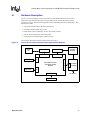
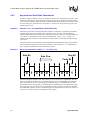
The basic structure of an inverter is shown in Figure 1.
Figure 1.
Basic Structure of an Inverter
AC-DC
CONVERSION
DC-AC
CONVERSION
INDUCTION
MOTOR
AC SINGLE
PHASE
Converter
Smoothing
Inverter
Circuit
Circuit
Circuit
IM
60 Hz
Control Circuit
Inverter
T1 & T2 ON
T3 & T4 OFF
0
VDC
AC with fixed frequency
6
T1 & T2 OFF
T3 & T4 ON
DC
2
AC with variable frequency
Application Note
Inverter Motor Control Using the 8xC196MC Microcontroller Design Guide
Varying the switching time controls the frequency of the AC output from the inverter. The
switching time can be controlled using a sinusoidal pulse width modulated (PWM) signal as
illustrated in Figure 2.
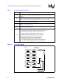
Figure 2.
Sinusoidal Waveform Generation Example
Carrier Frequency
8XC196MC/MD
WG1
Power Driver
Circuitry
+Vsupply
WG1#
U Phase
WG2
WG2
3 Phase
AC Induction
Motor
VDC
Q1
U
V Phase
WG2#
WG3
Modulating Waveform
120 o
WG2#
Q2
W Phase
VDC
V
WG3#
120o phase
shift from
each other
120 o
-Vsupply
VDC
W
3 phase PWM inverter
This method employs a PWM signal to enable or disable the transistors. In the example, the
8xC196MC microcontroller is used to produce the PWM signal. The switching points of the PWM
signal are determined by the intersection of the fixed-frequency triangular carrier wave and the
reference modulation sine wave. The output frequency is at the sine-wave frequency and the output
voltage is proportional to the magnitude of the sine wave.
The on-chip waveform generator (WFG) of 8xC196MC allows generation of three independent
complementary PWM pairs (with switching times determined by the method previously
discussed). The WFG is divided into three functional areas: the timebase generator, the phase
driver channel and the control section. For a detailed description of the WFG, refer to the
application note, AP-483, Application Examples Using the 8xC196MC/MD Microcontroller and to
the 8xC196 MC/MD/MH Microcontroller User Manual.
Application Note
7
Inverter Motor Control Using the 8xC196MC Microcontroller Design Guide
2.2
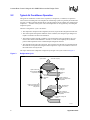
Typical Air Conditioner Operation
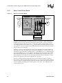
The typical air conditioner consists of an evaporator, a compressor, a condenser, an expansion
valve and two circulating fans. The complete air-conditioning system can generally be divided into
two parts; an indoor unit that channels the air into the premises and an outdoor unit containing the
compressor — the heart of the system. The room temperature can be regulated by controlling the
compressor speed.
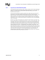
The basic “refrigeration” cycle is as follows:
• The compressor compresses the refrigerant (freon-22) vapor and the refrigerant becomes hot.
• The coolant passes through the condenser. In the condenser, the refrigerant gas changes into
liquid as it transfers its heat to the outside air.
• The refrigerant passes through a capillary valve and becomes cold. The capillary valve is a
narrow valve whose inside diameter is 1.0 mm to 1.5 mm. In the capillary valve, both the
pressure and temperature of the condensed liquid refrigerant decrease.
• The cold refrigerant enters the evaporator. The evaporator uses the heat of vaporization from
the inside air to evaporate the refrigerant from a liquid to a vapor. The cooled air is blown to
the inside of the room by the fan.
The vapor returns to the compressor to begin the cycle again. The cycle is shown in Figure 3.
Figure 3.
Refrigeration Cycle
Liquid coolant
Air forced out (48 C)
Condenser
Liquid coolant at
high temperature
and pressure
Condenser
cooling fan
4
Liquid
accumulator
Outside air
(35 C)
3
Expansion
valve
Coolant in gaseous
state at high temperature
and pressure
1
Coolant in practically liquid
state at low temperature
and pressure
Air delivered to
room (15 C)
2
Evaporator
Coolant in gaseous
state at high temperature
and pressure
Evaporator Cooling Fan
(+3 C)
A4760-01
8
Application Note
Inverter Motor Control Using the 8xC196MC Microcontroller Design Guide
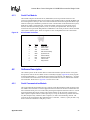
A control valve is used to switch the air conditioner from cooling mode to heating mode. The
operation of the control valve is shown in Figure 4. A typical system with a control valve is shown
in Figure 5.
Figure 4.
Air Conditioner's Operation in Cooling/Heating Mode
[INSIDE]
Evaporator
[OUTSIDE]
[INSIDE]
[OUTSIDE]
Control
Valve
Evaporator
Condenser
Cool
Wind
Warm
Wind
Cool
Wind
Warm
Wind
Condenser
Compressor
(a) COOLING MODE
Figure 5.
(b) HEATING MODE
Typical Air Conditioner
Outside Heat
Exchanger
Control
Valve
Fan
Inside Heat
Exchanger
Compressor
Capillary Valve
Fan
Application Note
9
Inverter Motor Control Using the 8xC196MC Microcontroller Design Guide
2.3
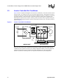
Inverter Controlled Air Conditioner
Figure 6 shows a simple block diagram of an inverter air conditioner. An inverter is used to control
the speed of the AC compressor motor by varying the supply frequency. The higher the frequency,
the faster the compressor rotates and the more the air conditioner warms or cools the air. To control
the supply frequency, a microcontroller is required to produce the three-phase complementary
PWM signals required for the transistor switching. These waveforms must be generated using the
sinusoidal PWM technique with three reference sinusoidal waveforms, each 120° apart in phase as
shown in Figure 2.
Figure 6.
Inverter Controlled Air Conditioner
Converter
Power Relay
Inverter
AC Single
Phase
Compressor
Motor
U
V
W
U
V
W
DRIVER
~
8XC196KB
3 Phase
AC Induction
Motor
Complementary
PWM Output
Serial
Interface
INDOOR UNIT
Driver
8XC196MC
OUTDOOR UNIT
When the room requires only a small amount of heating or cooling, the inverter enables the airconditioning unit to operate at a lower level, with the compressor rotating at a slower speed. The
compressor revolutions can be increased as the inside temperature rises. This cost-effective
measure consumes the minimum power level required to maintain the desired temperature.
10
Application Note
Inverter Motor Control Using the 8xC196MC Microcontroller Design Guide
2.4
Compressor Motor (AC Induction) Speed Control
In the inverter air-conditioner control scheme, the voltage/frequency ratio is typically held
constant. As previously described, the speed of an AC motor is proportional to the supply
frequency. As the compressor motor speeds up (higher frequency) the motor consumes more power
(higher voltage input), thus producing a greater amount of torque. The effect of this on the PWM
switching waveforms can be observed in Figure 7.
Figure 7.
Effect of Frequency Variations on the PWM Waveforms
FREQ. = 0.6 fmax
dm = 0.6
0
2
wt
Lower Frequency (more pulses)
V/F =
CONSTANT
FREQ. = 0.8 fmax
dm = 0.8
0
2
wt
Higher Frequency (less pulses, pulse width bigger)
When the frequency increases, the pulse width increases and the modulation depth, dm, also
increases. The pulses change more rapidly and a larger change is observed. The opposite happens
when the frequency decreases.
Application Note
11
Inverter Motor Control Using the 8xC196MC Microcontroller Design Guide
3.0
Designing an Inverter Air Conditioner with the
MCS® 96 Controller
Two MCS 96 controllers are used:
• An 8xC196KB controller is used in the inside unit monitors temperature settings and controls
the fan motors
• An 8xC196MC controller is used in the outside unit controls the compressor motor speed and
the direction of coolant flow
The operation of these controllers is described in the following sections.
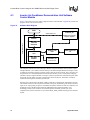
3.1
Inside Unit
On the inside unit, the 8xC196KB performs the following functions (see Table 1):
•
•
•
•
Controls flap/DC fan motors
Monitors the setpoint of room temperature through a wireless remote controller
Monitors room/coil temperature through the use of thermal sensors
Compares the room temperature setpoint with the monitored value and sends the frequency
command to the outside unit through a serial communication line.
The flap motor is a stepping motor; the fan motor is typically a DC brushless motor which is a type
of synchronous motor with a permanent magnet. Figure 8 shows a block diagram.
Table 1.
Signal Descriptions for the 8xC196KB (Inside Unit)
8xC196KB
Signals
Function
Description of Function
A/D
ACH.0
ACH.1
ACH.2
ACH.3
ACH.4
ACH.5/6/7
Monitor room temperature
Monitor heat exchanger temperature
Read a setpoint value
Read a setpoint value
Monitor room humidity
Not used
HSO
HSO.0 through 5
Drive power transistor module of fan motor
HSI.0
Detect induced electromagnetic voltage of fan motor to
monitor the pole position of rotor
HSI
HSI.1
PWM
Control the DC voltage source which is supplied to the
fan motor to vary the motor torque
Port 1
Receive setpoint conditions from power select switch
Port 2
Read setpoint value
Port 3
Control LED display
RXD/TXD/
EXTINT
12
Receive remote controller data
Communicate with the controller of outside unit
Application Note
Inverter Motor Control Using the 8xC196MC Microcontroller Design Guide
Figure 8.
Electrical Circuit Block Diagram Of Inside Unit
DRIVER
4
4 PHASE STEPPING
MOTOR FOR
FLAP
DC Voltage Source
Controller
PORT 4
Analog
Channel
SENSORS
(Room Temperature, Coil
Temperature, Humidity)
MCS-96
PWM
HSI
Receiver
Remote Controller
8XC196KB
Port 3
LED
Driver
LED Display
HSI
Port 1
Power
Transistor
HSO
TXD
RXD
EXTINT
3 Phase DC
Brushless Motor
for FAN
Application Note
Switch Panel
From / To
PHOTO-COUPLER
Outside Unit
13
Inverter Motor Control Using the 8xC196MC Microcontroller Design Guide
3.2
Outside Unit
On the outside unit, the 8xC196MC performs the following functions (see Table 2):
• Controls the compressor motor, which is controlled by using the V/F control algorithm and
sinusoidal wave PWM technique.
• Monitors with thermistors the outside/compressor/heat-exchanger temperature to recognize
abnormal conditions.
• Controls the control valve to change direction of coolant flow.
• Controls the capillary valve to change the inside diameter.
A three-phase induction motor is used as compressor motor. A stepping motor controls the
capillary valve. A block diagram is shown in Figure 9.
The 8xC196MC controller has the sine table to perform the sinusoidal wave PWM and V/F pattern
in the internal memory. When the controller in the outside unit receives the frequency command
from the controller in the inside unit through the serial communication line, the outside unit’s
controller knows the output voltage of the inverter from V/F pattern and creates the equivalent
PWM pulse in sinusoidal wave using the sine table.
The PWM pulses are output from the 8xC196MC controller’s six Waveform Generate output pins.
The waveform generator can produce three independent pairs of complementary PWM outputs that
share a common carrier period, dead time and operating mode.
The waveform generator has three main parts: a timebase generator, phase driver channels and
control circuitry. The time base generator establishes the carrier period, the phase driver channels
determine the duty cycle and the control circuitry determines the operating mode and controls
interrupt generation. For additional information and application examples, consult AP-483,
Application Examples Using the 8xC196MC/MD Microcontroller.
Table 2.
14
Signal Descriptions for the 8xC196MC Outside Unit
8xC196MC
Signals
Function
Description of Function
A/D
Ach.0
Ach.1
Ach.2
Ach.3
Ach.4/5/6/7
Monitor heat exchanger temperature
Monitor compressor temperature
Monitor outside temperature
Monitor current of smoothing circuit
Read setpoint value and for test
WG (Port 6)
WG1 to WG3
WG1# to WG3#
Drive photocoupler driver for compressor motor (threephase induction motor)
Port1
Read setpoint value
Port3
Control fan speed, control valve, electromagnetic valve
and similar functions
Port4
Control stepping motor of capillary valve
RXD/TXD/
EXTINT
Communicate with the controller of outside unit
Application Note
Inverter Motor Control Using the 8xC196MC Microcontroller Design Guide
Figure 9.
Electric Circuit Block Diagram Of Outside Unit
PORT 4
DRIVER
Analog
Channel
4 PHASE STEPPING
MOTOR FOR
CAPILLARY VALVE
SENSORS
(High exchanger Temp, outside
Temp, Compressor Temp)
MCS-96
87C196MC
+Vsupply
U phase
Q1
WG2
W phase
3 PHASE
AC INDUCTOR
MOTOR
WG2#
CONTROL :
Fan Speed
Control Valve
Electromagnetic Valve
WG3
WG3#
-Vsupply
Power Driver
Circuitry
1 0f 3
Application Note
Port 3
WG2
WG2#
V phase
Q2
WG1
WG1#
TXD
RXD
EXTINT
From / To
PHOTO-COUPLER
Inside Unit
15
Inverter Motor Control Using the 8xC196MC Microcontroller Design Guide
3.3
Dead Time
Dead time is defined as the time in which both transistors of the upper arm and lower arm turn off,
as show in Figure 10. The dead time is implemented to protect the power transistor module from
through current when both transistors of a phase are turned on.
Because there is no hardware limit on minimum PWM pulse width, it is also possible to deassert
one of the WFG outputs for the entire PWM period if the total dead-time is longer than the pulse
width. For this reason, there should be a software limit check preventing the pulse width from
being less than 3x the dead time.
Figure 10.
U-Channel Motor Driver Block Diagram
5V
U Phase
0V
TON
TOFF
5V
U Phase
0V
dead time
= 10 µs
16
Application Note
Inverter Motor Control Using the 8xC196MC Microcontroller Design Guide
3.4
Protection Circuitry
The protection circuitry allows all WFG outputs to be simultaneously deasserted under software
control or in response to an external event. This same external event also generates the EXTINT
interrupt, allowing software to stage a graceful recovery from an external error condition.
Figure 11.
Protection Circuitry
EXTINT
Interrupt
Request
ES, IT
DP
Falling
Transition
Detector
Rising
EO BT
Register
00
01
Pulse
EXTINT
R
OD#
Q
Low
Fxtal
Level
Sampler
High
10
S
11
CPU Write EO
CPU Read EO
CPU Bus
A4758-01
Application Note
17
Inverter Motor Control Using the 8xC196MC Microcontroller Design Guide
4.0
Project Overview
The previous sections provided an overview of how to use MCS®96 controllers to create an
inverter controlled air-conditioning system. This section describes a demonstration unit that
provides a working example which uses the peripherals in the 8xC196MC microcontroller to
handle inverter motor control in an air-conditioning system.
The main purpose of the Inverter Motor Control Demonstration Unit (Figure 12) is to show that the
8xC196MC microcontroller is suitable for use in an inverter controlled air-conditioner control
system. This demonstration unit consists of a control unit, a motor unit, and a host PC.
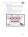
Figure 12.
Inverter Motor Control Demonstration Unit
HOST PC
CONTROL UNIT
MOTOR UNIT
196MC
Control Board
Serial
Communication
Power Board
Sensor
Feedback
3-phase
PWM
waveform
AC Induction
Motor
Generally, the host PC provides the user interface and transmits the inputs serially to the control
unit of the demonstration system. The control unit contains the control board and power board. The
8xC196MC microcontroller, which resides in the control board, processes the transmitted request
from the host PC. The response signals output from the waveform generator of the microcontroller
drive the inverter module in the power board to produce a variable frequency signal suitable for
powering the three-phase AC Induction Motor. The effect of this change can be observed at the
output of the motor unit through the speed of the blower driven by the AC Induction Motor. The
8xC196MC controller also interprets the sensor feedback from the motor unit and displays the
motor speed on an LED display.
18
Application Note
Inverter Motor Control Using the 8xC196MC Microcontroller Design Guide
4.1
Hardware Description
Figure 13 is a block diagram of the Inverter Motor Control Demonstration Unit. The main
component in the demonstration unit is the 80C196MC motor control demo board, which
interfaces to various subsystems through ribbon cable-compatible dual-in-line header plugs. The
subsystems include:
•
•
•
•
•
A power board which drives the three-phase motor
Switches to enable manual user control
Panel meters and an LCD display to show the system variables
Sensors which feed back the state of the motor
A Serial port for communication with the host PC
The interface signals between the systems are listed in Table 3.
Figure 13.
Inverter Air-Conditioner Demonstration System Block Diagram
HOST
PC
DISPLAY
SERIAL PORT
SENSORS
P6
P2
P1
80C196MC MOTOR
CONTROL DEMO
BOARD
METERS
3 PHASE
MOTOR
P
10
P3
POWER
BOARD
P9
P8
AC INPUT
SWITCHES
Application Note
19
Inverter Motor Control Using the 8xC196MC Microcontroller Design Guide
Table 3.
Connector Signal Description
PLUG
DESCRIPTION
P1
60-pin connector containing, among other signals, the output signals of Port 3 and Port 4.
These ports drive the 4-line by 20-character LCD display. The connections are shown in
Figure 13.
P2
10-pin connector with signals for monitoring the digital motor sensors to measure position and
RPM. The sensor interfaces the microcontroller through Port 1.2, Port 1.3, Port 2.2, and Port
2.4. The current software only implements the input to Port 1.2 for the motor RPM.
P6
50-pin connector providing general I/O plug which links the microcontroller and the serial port.
Port 2.1 is the RXD pin and Port 2.6 is the TXD pin.
P8
16-pin connector providing the interface to the control pushbuttons and switches. Its
connections are shown in Figure 14.
P9
16-pin connector that interfaces PWM0 (P9-8) and PWM1 (P9-9) to the panel meters that
display frequency and volts/Hz ratio.
40-pin connector containing the motor control signal routed to the power board.
P10 outputs: Waveform generator outputs which drives the power board
• WG1# and WG1 produce AHI# and ALO# on P10-14 and 16
• WG2# and WG2 produce BHI# and BLO# on P10-20 and 22
P10
• WG3# and WG3 produce CHI# and CLO# on P10-26 and 28
P10 inputs: Feedback and status signal from the power board
• RUNNING (P10-4) goes to the 80C196MC EXTINT pin
• CPU Requested (P10-6) goes to the 80C196MC Port 2.0
• IA, IB and IC are the analog phase currents on P10-34, 36 and 38
• ISEN on P10-32 is the amplified sum of the three phase currents
Figure 14.
P1 to Display Wiring
P1
2
4
6
8
10
12
14
16
18
20
22
24
55
DISPLAY
Vcc
D0
D1
D2
D3
D4
D5
D6
D7
COMMON
D8
D9
-V
2
7
8
9
10
11
12
13
14
1, 5
6
4
30k
20k
30k
C
O
N
T
R
A
S
T
3
15
20
Application Note
Inverter Motor Control Using the 8xC196MC Microcontroller Design Guide
Figure 15.
P8 Control Switches Interface
P8
2
4
6
8
10
12
14
16
Application Note
STOP PB
ACH3
ACH4
ACH5
ACH6
ACH7
RESET#
PORT 7.3
Vcc
Increment PB
Decrement PB
Freq. / Slope SW
Disable/Enable SW
Forward/Reverse SW
21
Inverter Motor Control Using the 8xC196MC Microcontroller Design Guide
Figure 16.
Inverter Air-Conditioner Demonstration Set (Top View)
FREQUENCY
METER
INVERTER MOTOR
DEMONSTRATION UNIT
SERIAL
PORT
VOLT/HZ
METER
80C196MC
Motor Control
Board Logic
MOTOR RPM
METER
4 LINE x 20
CHARACTER DISPLAY
< PWM PERIOD >
< % POWER >
< FREQUENCY OUTPUT >
< MOTOR RPM >
SENSOR
FEEDBACK
LO-V
Power Board
HI-V
RESET
ON
FORWARD
VOLTS/HZ RATIO
REVERSE
FREQUENCY
START
UP
OFF
22
DOWN
Application Note
Inverter Motor Control Using the 8xC196MC Microcontroller Design Guide
4.1.1
80C196MC Motor Control Board Logic
The Motor Control Board schematic and the component layout diagram are included in
Appendix A, “Schematics.” The reset circuit causes a chip reset in four ways: at power up, from
the reset pushbutton, from an external input on RESET#, or internally from the 80C196MC. The
timings for the demo board are based on the 16 MHz XTAL circuit.
Note:
Board locations referenced in this section are shown in the schematics in Appendix A.
The 80C196MC has seven I/O ports: Port 0 - Port 6:
• Port 0 is used as an analog input-only port. Signals at this port are connected as follows:
Table 4.
I/O Port Connections
Signal
Connection
ACH0, ACH1, ACH2
Any three of ISEN, IA, IB, or IC (as selected by jumpers E8, E9 and E10)
ACH3
Increment Switch
ACH4
Decrement Switch
ACH5
Frequency / Slope (volts/hz) Switch
ACH6
Enable / Disable Switch
ACH7
Forward / Reverse Switch
• Port 1 contains five additional analog/digital input-only bits. P1.0 is a serial input on plug P3.
P1.2 and P1.3 go to plug P2 from digital motor sensors. The demo system only uses the P1.2
input, which gives the motor RPM. These signals appear on the general purpose plug, P6.
• Port 2 is the capture/compare I/O associated with EPA. P2.0 is used for CPU_REQ while P2.2
and P2.4 are the other motor sensor inputs. The current demo does not implement these two
sensor feedback. Meanwhile, P2.5 provides the additional PWM signal needed to control the
RPM panel meter. P2.1 and P2.6 are involved in the serial interface module as the receiving
and transmitting pin respectively. All these port 2 signals also appear on plug P6.
• Port 3 is the low-order address/data lines for the external bus. There is no external bus during
demo operation and these lines are the data interface to the LCD display. These lines have
pull-up resistors and appear on plug P1.
• Port 4 is the high-order address/data lines for the external bus. P4.0 switches between data
(P4.0 = 1) and commands (P4.0 = 0) for the LCD display. P4.1 is a load enable (1) / disable (0)
signal for the display. These lines have pull-up resistors and appear on plug P1.
• Port 5 signals control the external bus and appear on plug P1. The demo unit does not use the
external bus.
• Port 6 contains signals corresponding to Waveform Generator (WG) and PWM logic. The WG
signals control three-phase voltages to the AC motor and appear on P10 after U6 buffers them.
The PWM signals appear on P9 and go to the panel meters indicating frequency and volts/Hz.
One last block of logic involves U7. This “wired-or” circuit can shut off the motor by deasserting
RUN#. There are two sources:
• When the WG turns on both outputs of a complementary output pair at the same time
• The RESTART button is pressed
The fact that there is so little circuitry on the 80C196MC demo board demonstrates how wellintegrated the 80C196MC is. The only external circuits needed are the U6 buffers and U7 interlock.
Application Note
23
Inverter Motor Control Using the 8xC196MC Microcontroller Design Guide
4.1.2
Motor Control Power Board
Figure 17.
Motor Control Power Board
CONVERTER
AC POWER
SUPPLY
120 V ac
60 Hz
RECTIFIER
INVERTER
340 V dc
IGBT MODULE
U
V
Z
_
U
_
V
_
Z
COMPRESSOR
MOTOR
M
GROUND
POWER BOARD
DRIVER
COMPLEMENTARY
PWM OUTPUT
WAVEFORM GENERATOR
80C196MC
The Motor Interface Schematic is available in Appendix A, “Schematics.” Sheet 1 shows the
schematic for the AC to DC conversion portion of the inverter circuitry. The AC provides highvoltage (approximately 340 V DC) at TP26. J1 can be used to enable a voltage doubler circuit. A
low-voltage regulator circuit provides a +15 VDC supply voltage at TP4. The logic devices on this
board operate at +15 V DC for improved noise immunity. Ratings and notes for the power board are
listed on Sheet 3 of the schematics.
On sheet 2, U5 and U6 form the protection circuitry. The compliment of RUNNING enables the
three-phase driver logic. The enable signal from the demo board, RUN# = 0, turns on the U5 flipflops which results in CPUREQ = 0 and RUNNING = 1. When RUN# goes to a 1, RUNNING goes
to a 0 and CPUREQ goes to a 1. Also, when the total phase current goes too high, it turns off the
RUNNING flip-flop while leaving CPUREQ= 0. The CPUREQ signal is helpful for debug, as it
shows whether an over-current error or a CPU request turned the motor off. ISENSE is an analog
output showing the sum of the current through the lower transistors.
Sheets 3 to 5 contain the phase driver electronics. Since these sheets are similar, we will only
discuss Sheet 3. The high and low phase enable signals go to U1 and continues to the high and low
drivers, Q1 and Q4. Q1 supplies the high voltage drive available on TP25. Q4 supplies the common
low drive at TP24. The buffered phase current appears at TP15. TP15 - TP17 contain the phase
current signal test points.
24
Application Note
Inverter Motor Control Using the 8xC196MC Microcontroller Design Guide
4.1.3
Serial Port Module
The module comprises an RS-232 driver (MAXIM 233) and a 9-pin female connector. The
received or transmitted data at the serial connector enters the RS-232 driver through the R2IN and
leaves through the T1OUT pin. The receive data is buffered to obtain the output at the R1OUT pin
while the T1IN input is buffered to produce the T1OUT transmit data. In the demonstration system,
the R1OUT output is connected to P2.1 of the 80C196MC, which serves as the serial receive
channel, while the transmitting channel, T1IN, is currently not implemented. The T2IN pin is
connected as the input for the Ring Indicator and R2OUT is the status pin which contains the Data
Carrier Detect (DCD) signal. These two signals are also not implemented on the current demo.
Figure 18.
4.2
9-Pin Female Connector
Pin
Name
1
CD
Description
Carrier Detect
2
RXD
Receive Data
3
TXD
Transmit Data
4
DTR
Data Terminal Ready
5
GND
System Ground
6
DSR
Data Set Ready
7
RTS
Request to Send
8
CTS
Clear to Send
9
RI
Ring Indicator
Software Description
The software portion of the Inverter Motor Control Demonstration System consists of two parts:
the operation code for the 8xC196MC written in assembly language (Appendix B) and a program
created using Borland* C++ to handle the user interface at the host PC. The Borland C++ program
can establish a serial link with the control board, which enables the user to communicate with the
microcontroller. Please refer to Appendix C for the source code.
4.2.1
Serial Communication Module
This serial communication module sets up a software serial data transmission and reception on the
8xC196MC microcontroller. A software approach had to be used since the microcontroller does not
have a hardware serial port. This is achieved by utilizing the Peripheral Transaction Server ‘s Serial
Input Output (PTS SIO) mode, together with an EPA channel. In the programs created, Port 2.1
(EPA Capture Compare Channel 1, EPA CapComp1) is set up as the receiving channel while Port
2.6 (EPA Compare Only Channel 2, EPA Compare 2) is used as the transmitting channel. The
protocol for this asynchronous data communication is 7 data bits, 1 start bit, 1 parity bit and 1 stop
bit at a baud rate of 9600 bit/s. Odd parity is used.
Application Note
25
Inverter Motor Control Using the 8xC196MC Microcontroller Design Guide
4.2.2
Asynchronous Serial Data Transmission
The EPA Compare 2 channel is set up to generate the time base for outputting the serial data, thus
determining the baud rate. Transmission is started by clearing the output pin, which generates the
“start” bit (0). The EPA Compare 2 module is loaded with the time at which the first data bit should
be driven to the port. This time must correspond to 1 “bit time” for the baud rate being used. The
formula used to this is:
Equation 1.
VALUE = FXTAL / (4 x BAUD RATE x EPA_PRESCALE)
Each time a timer match is made between EPA Compare 2 and Timer1, an interrupt is generated.
The PTS outputs the next bit of data on the output pin; in this case, P2.6. The asynchronous
transmit mode automatically transmits the 7 data bits followed by a parity bit, and terminated by a
“stop” bit (1). A maximum of 16 bits can be transmitted (data + parity + stop = 16 max.). To
transmit 7 data bits with parity, a total of 9 PTS interrupt and one conventional (end-of-interrupt)
cycles occur.
Note that the data to be transmitted is right-justified in the PTSCB DATA0 register, and is shifted
out least significant (right-most) bit first. For example, an ASCII character “1” is transmitted as
below using this asynchronous serial transmission program:
Example 1.
Binary representation for ASCII “1” → 011 0001 (31h)
Start Bit
Data Flow
Stop Bit
Parity Bit
0 1 0 0 0 1 1 0 0 1
The final interrupt is called the end-of PTS interrupt. This interrupt occurs immediately after the
stop bit is outputted, and takes the conventional interrupt vector to COMPARE2_INT, where the
PTS control block is serviced. In this program, the DATA0_W0_L is loaded with the next data
byte, PTSCOUNT is reloaded with 9, and PTSCON10 is reloaded. Then, clearing the P2.6 creates
the “start bit” for the next data word to be transmitted. The EPA Compare 2 channel is initialized,
and COMPARE_TIME is written to, establishing the time which the first bit of the next word is to
be driven out. A total of 4 bytes is transmitted in this program.
26
Application Note
Inverter Motor Control Using the 8xC196MC Microcontroller Design Guide
4.2.3
Asynchronous Serial Data Reception
In the program developed, the EPA CapComp 1 channel is initially used in the capture falling edge
mode to receive the data “start” bit input (a falling edge transition from “1” to “0”) on P2.1. This
generates a conventional interrupt (the same as the “end-of PTS interrupt) which starts the
asynchronous receive process.
This initial interrupt changes the CapComp 1 module to the compare mode, sets the time of the
next compare to 1.5 bit times and enables the PTS. Thus, at exactly 1.5 bit times from the
beginning of the start bit the first PTS cycle will sample the input data on P2.1 and shift it into the
DATA1_W0 register. This software also uses the majority sampling mode, thus an additional
sample is taken. If the two samples are different, the data is sampled one more time to determine
which polarity is correct. The time between samples is controlled by the value of the SAMPTIME
register in the PTSCB.
Each PTS cycle samples the input data at P2.1 and shifts the value into DATA1_W0 register. The
time interval between the cycle establishes the baud rate. To receive 7 data bits with parity, a total
of nine PTS cycles and two conventional interrupts occur. During the conventional interrupt, the
CAPCOMP1_CON register is read to determine if it is the initial or final (end-of PTS) interrupt.
This could be achieved by determining when the software is in the capture or compare mode. Thus,
when the capture mode is active — indicating that this is the initial “start” bit interrupt — the
CapComp1 module is switched to the compare mode, and CAPCOMP1_TIME is loaded with the
time to sample the first data bit (1.5 bit times). The PTS is enabled, and the routine returns to a loop
waiting for the rest of the data bits to be received. Else, if the compare mode is selected indicating
a final (end-of PTS) interrupt, checking for parity and framing error is done and DATA1_W0
(which contains the incoming data) is stored in the RECEIVE buffer. Then the module is reinitialized and EPA CAPCOMP1_COM is set to the capture falling edge mode, thus readying P2.1
to wait for the next start bit. A total of 4 bytes are received.
Application Note
27
Inverter Motor Control Using the 8xC196MC Microcontroller Design Guide
4.3
Inverter Air-Conditioner Demonstration Unit Software
Control Module
Figure 19 provides an overview of the complete software control module. Appendix B provides the
program source code for this software.
Figure 19.
Software Block Diagram
BEGIN
COMPARE0_INT
ENABLE SWITCH OFF
Update wave generator
compare registers
INITIALIZE
REGISTERS
ENABLE SWITCH ON
ENABLE SWITCH OFF
RESTART
IDLE TIME
LOOP
GET NEW
REQUEST
CHANGE_FLAG
BYTE
TIMER_OVERFLOW
INT
CAPCOMP1_INT
Serial Data Input
The complete software uses three interrupts: the EPA Compare Module 0 Interrupt, EPA Capture
Compare Module 1, and Timer Overflow interrupt. The EPA Compare Module 0 interrupt is used
to update the waveform generator compare registers after each carrier period. This is necessary for
the generation of a sinusoidal PWM waveform because the duty cycle is continuously changing.
The EPA Capture Compare Module 1 interrupt is used for asynchronous serial data reception from
the host PC and the Timer Overflow interrupt keeps track of real time. The blocks of software
communicate through the CHANGE_FLAG byte.
Generally, the software enters the IDLE_TIME_LOOP after completing the initialization routines.
The software remains in this loop until a software (serial port) or hardware (push-button switches)
input occurs. Upon getting an input, it recalculates the system variables for this new condition. The
peripherals, such as the Waveform Generator, PWM Generator and EPA modules, react
accordingly, based on the condition conveyed through the CHANGE_FLAG byte. Upon
completion, the software continues to cycle in the IDLE_TIME_LOOP, awaiting the next external
request.
28
Application Note
Inverter Motor Control Using the 8xC196MC Microcontroller Design Guide
4.4
Detailed Description of the Software Listing
Appendix B contains the complete source listing of the Inverter Motor Control Demonstration Unit
Software module. The DEF196MC.INC defines the 80C196MC Input/Output and Special
Function registers. It also declares some items as public, for the use of other modules, and defines
all interrupt and PTS vector locations. The PTS control block and its corresponding windowed
locations are defined here too.
The following are the few associated concepts in the main program code:
• Memory location 40h through 58h contains the variables used for the serial reception and
decoding of the data from the host PC. The RECEIVE array contains the data in bytes that is
successfully received without parity or framing array. Variable R_COUNT controls the
number of bytes received in one cycle and HZ contains the decoded frequency (x 100) input.
• A sine lookup table contains 960 word entries. THETA_360 is the number of sample times in
360 degrees and THETA_60 is the number of sample times in 60 degrees. The motor control
parameters have limits and the program has many min_xxxx and max_xxxx constants. The
constants half_xxxx corresponds to half cycles.
• The program defines a a variable named VOLTZ_HZ along with its associated max/min
constants. As the frequency of the motor increases, the applied voltage must be adjusted to
compensate for the changing motor reactance. VOLTZ_HZ is the value that sets the slope of
the volts applied as frequency increases and roughly corresponds to the torque. Controlling the
rate of frequency change avoids excessive currents by ensuring the motor does neither stalls
nor becomes a generator. In inverter motor, this VOLTS_HZ ratio is usually set as a constant.
• The frequency value which corresponds to the speed of the AC compressor motor is stored in
the program in the HZ_OUT variable. The value stored is the frequency x 100, not the actual
frequency. This is to enable higher precision of speed control of the AC motor. HZ_x100
contains the frequency x 100 values inputted by the user, via hardware or software. The
restricted value, taking into account the limits of the motor, is stored in the HZ_OUT variable.
This is the frequency at which the motor is operating.
The main program starts at location 2080h, to which the processor branches following the reading
of the CCB bytes. The subsequent code contains the BEGIN software, the RESTART software and
the IDLE_TIME_LOOP software. Here, the software looks for the input from the push buttons or
the host PC, and sets flags that determine what the program will do next. The flags are set by the
interrupt routines and the software code. The remainder of the source code contains the program
subroutines and the interrupt service routines. The sine lookup table starts at location 3800h in the
program and contains 2048 bytes of data.
When the demo first is powered-up, the BEGIN software is executed. This software initializes the
LCD and clears the register RAM (location 40h to E0h). This BEGIN software needs to be
executed only once.
Next, the RESTART software initializes the system variables and operating modes. This software
is re-executed every time the restart button is pressed. First, the interrupt is disabled and the
interrupt mask registers are cleared. Then, the INITIALIZE_REG subroutine is called before the
software stops to wait for the enable switch to be turned on.
In the INITIALIZE_REG subroutine, the C8h that goes in the T0_CONTROL register enables the
timer/counter as an up counter, sets the clock source to external, and sets the resolution to the
250 ns maximum. Setting T1_CONTROL to a C1h selects an up count, internal clock source, and
500 ns resolution. The next instruction sets the PWM0 and PWM1 period to 256 states. Then a
Application Note
29
Inverter Motor Control Using the 8xC196MC Microcontroller Design Guide
section initializes the wave generator and associated variables. Finally, the software clears any
pending interrupts and initializes the TMP_OVR_CNT and the debug pointer. It then returns
control to the RESTART software.
The software waits until the enable switch is turned on and the motor is stopped. This prevents
damage that can occur when the motor runs while applying a voltage at a very different frequency.
Assuming that the conditions are met, the program sets up for motor control with a call to
GET_VALUES, which consists of the following code:
GET_VALUES:
CALL
VALUE CHANGE
CALL
SET_FREQ_WITH_PUSHA
SET_FREQ_WITH_PUSHA:
PUSHA
BR
SET_FREQUENCY
This structure is only used during initialization and does not occur again after the program is up
and running. The above code uses the interrupt run-time subroutines during the startup phase
before enabling interrupts.
During normal operation, the VALUE_CHANGE routine executes as a part of the
GET_NEW_REQUEST routine. During initialization, there is no “new” request, so
VALUE_CHANGE executes directly. This routine controls the PWM0 and PWM1, which serves
as indicators of frequency (HZ_x100) and the slope of the output volts to output frequency ratio
(VOLTS_HZ). VALUE_CHANGE checks these variables for an overflow condition and routes
frequency to PWM0 and slop to PWM1. These signals go the panel meters. Subsequently,
VALUE_CHANGE compares the present output frequency, HZ_OUT, with the new input,
HZ_x100. If they are equal, no action is necessary. Otherwise, the program calculates the new
values of the associated variables, sets CHANGE_FLAG.0, and outputs the new values to the LCD
display. The LCD display module is separated from the motor control module and is optional.
Next, the subroutine SET_FREQUENCY, part of the COMPARE0_INT interrupt subroutine, is
executed. The reason for the above initialization code is now apparent: we have caused the
software to execute part of the interrupt code even though no interrupt has occurred. The wave
generator register buffer update occurs and if PERCENT_PWR is too high, the software calls the
ERROR routine. In the error routine, the error will be trapped until the enable switch is turned off.
The program then branches to RESTART. Either action will shut the motor down. If the value in
PERCENT_PWR is acceptable, the software calculates the new PWM phase values, checks their
integrity, and stores them to await the next COMPARE0_INT. If the reverse switch is in the reverse
position, the software swaps the values of phases B and C.
The initialization process continues with the receive mode initialization. First, the PTS control
block is set up for the asynchronous serial data reception mode. Majority sampling is enabled and a
16-state sampling time is set. The EPA Capture Compare 1 module and its corresponding P2.1 port
pin is used for data reception. The EPA CAPCOMP1 is programmed to capture a negative edge to
mark the beginning of a reception. A baud rate of 9600 bit/sec is selected by writing D0h to the
BAUDCONST1_W0 register. Seven data bits, one stop bit and one odd parity bit is to be received.
Only 1 byte is received in one cycle.
Finally, the RESTART software writes to the interrupt mask register to enable the respective
interrupts. The motor power board and the interrupts are enabled and the motor enters the
IDLE_TIME_LOOP software.
30
Application Note
Inverter Motor Control Using the 8xC196MC Microcontroller Design Guide
At the IDLE_TIME_LOOP, RXDDONE is checked to see if any data has been received. Each byte
of data is sent three times from the host PC to ensure precise communication. A variable, TIMES,
is used to indicate the number of times a particular byte is received. Upon receiving three bytes of
data, the program enters a validation process. First, it will determine the number of valid data bytes
that have been received. A data byte is valid if there is no framing or parity error. This check is
done at the EPA CapComp1 module used for the serial I/O as part of its interrupt service routine.
The implementation of the EPA CapComp1 module for the asynchronous serial data reception is
discussed in detail in Section 4.2.3.
If there are two or three valid data bytes, they are compared with one another to determine if they
are the same. If there is a match between two received data bytes, then that data byte is used. If they
do not match, the error routine is called to indicate a serial communication error. When there is
only one valid data byte, then this byte would be used. The error routine is also called if there are
no valid data bytes. Upon obtaining the correct data byte, a decode routine is called to convert the
received ASCII byte into a hexadecimal digit. The decoded value is stored in the HZ_IN register.
The serial receive mode is re-initialized to wait for the next data byte. When four data bytes are
verified and decoded successfully, the value of HZ_IN is transferred in the HZ register. The value
in this register is the software frequency input from the host PC. Again, if the enable switch is off,
the program restarts and all registers are cleared.
The CHANGE_FLAG.1 indicates whether there is a timer overflow. IDLE_TIME_LOOP waits for
the timer overflow and fetches any new request after eight timer overflows. Every second, 61 timer
overflows occur, causing execution of the rest of the idle time loop.
The GET_NEW_REQUEST subroutines execute every eight timer overflows to fetch any new
request. This subroutine first checks for a software input, then checks the panel switches for a
hardware input. Input from either of these sources causes the program to increment or decrement a
corresponding variable. Values must be within the maximum and minimum limits. Note that the
software input has a priority higher than the hardware input in this demonstration unit. After
servicing the serial input and switches, the VALUE_CHANGE portion of the
GET_NEW_REQUEST subroutine starts the system with the initial parameter constants. After the
next Compare0 interrupt, nothing changes until the operator activates either the increase or
decrease push button while the enable switch is on.
The wave generator compare registers changes only at the beginning of the compare0 interrupt
service routine, COMPARE0_INT. After processing all the parameters, checking all possible error
conditions, and processing the serial and push button requests, the software updates the three wave
generator compare registers.
Application Note
31
Inverter Motor Control Using the 8xC196MC Microcontroller Design Guide
5.0
Related Documents
Document Title
32
Order Number
8xC196MC, 8xC196MD, 8xC196MH Microcontroller User’s Manual
272181
AP-483: Application Examples Using the 8xC196MC/MD Microcontroller
272282
Application Note
Inverter Motor Control Using 8xC196MC Microcontroller Design Guide
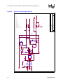
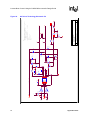
Appendix A Schematics
The following pages contain schematics for the Motor Control Demonstration Board discussed in
this application note.
Application Note
33
IC
IB
IA
ISEN
TP10
TP8
TP6
TP4
TP2
1
3
5
7
9
11
13
15
P9
2
4
6
8
10
12
14
16
18
20
22
24
26
28
30
32
34
36
38
40
2
4
6
8
10
12
14
16
18
20
2
4
6
8
10
12
14
16
10K
R23
10K
R25
10K
R29
10K
R27
CON20
1
3
5
7
9
11
13
15
17
19
CON40
(TO PANEL METERS)
GND
P2.5
IA
PWM0
ISEN
GND
ISEN
IC
(TO
POWER
BOARD)
1
3
5
7
9
11
13
15
17
19
21
23
25
27
29
31
33
35
37
39
TP9
TP7
TP5
TP3
P2.5
P2.5
GND
PWM0
IB
PWM1
PWM1
GND
C14
.001uf
C15
.001uf
C17
.001uf
C16
.001uf
TP1
ISEN
IA
IB
IC
CHI#
CLO#
BHI#
BLO#
AHI#
ALO#
IB
R30
5K
+15
PWM1
PWM0
R28
5K
P2.5
RUN#
RUNNING
CPU REO
R26
5K
R24
5K
C
1
3
1
VCC
1
3
2
E8
2
E9
2
JP12-4
JP12-3
ACH2
ACH1
P11-7
R17
R16
U4-43
U4-39
C5
.01uF
U4-43
1
P11-6
1
R15
C3
1.0uF
1
VCC
U1-7
U1-14
P11-2
C12
.01uF
RE-START
2
4
6
8
10
12
14
16
C6
.01uF
1
3
5
7
9
11
13
15
P8
2K
U4-4
U4-14
RESET#
47K
P11-3
47K
47K
U4-39
VCC
P7.0
P7.1
P11-18
R21
R20
P11-14
R19
R18
47K
47K
47K
47K
WG1#
WG1
WG2#
WG2
WG3#
WG3
P11-10
R22
(TO CONTROL
SWITCHES)
P7.3
.001uf
P11-15
.001uf
P11-11
.001uf
C7
22uF
C24
.001uf
C22
.001uf
C20
.001uf
RUNNING
ACH0
C23
C21
C19
E10
3
B
A
C
B
A
B C
34
A
13
12
9
8
6
5
2
1
U4-7
U4-14
18
17
16
15
14
13
12
11
10
C16
.01uF
74HC03
74HC03
U7D
74HC03
U7C
74HC03
U7B
U7A
ULN 2003
1
2
3
4
5
6
7
8
9
U8
+15
11
10
4
3
ACH3
ACH4
ACH5
ACH6
ACH7
VCC
TP10
RUN#
1
2
3
4
5
6
7
8
9
RESET#
680
AHI#
ALO#
BHI#
BLO#
CHI#
CLO#
R31
10K
COM
A
B
C
D
E
F
G
H
RP3
2
OPEN
8
7
U2C
E2
6
13
12
17
14
2
1
3
20
VCC
+5
VCC
R7
C1+
C1VVV+
T1IN
T2IN
R1OUT
R2OUT
U3
E1
C8
0.1uf
Document Number
EXP. BUSES & DOPL. COPS.
Monday, May 11, 1998
Date:
D4
1K
Size
A4
MOTOR CONTROL .1
10K
R14
6
5
R5
470
EXTINT
OPTO-4
12
1K
R4
VCC
11
+5
R6 470
CPU REQ
Title
1
R8
1K
OPTO-4
13
14
+5
15
OPTO-4
U2D
4
74HC14
U6A
9
10
1K
3 U2B
2 OPTO-4
16
D5
DIOD
1 U2A
R10
1K
R9
P2.6
10K
P1.0
R13
D3
LED
VCC
GND
VI
11
15
10
16
5
18
4
19
P2.0
MAX233
C2+
C2+
C2C2-
T1OUT
T2OUT
R1IN
R2IN
VO
Sheet
1
TXD2
RXD2
C1
22uf
of
1
3
5
7
9
P3
2
2
4
6
8
10
Rev
1.0
POWER CONNECTOR
1
2
3
4
P4
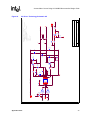
Figure 20.
I
P10
Inverter Motor Control Using 8xC196MC Microcontroller Design Guide
Motor Control Schematic 1/2
Application Note
Application Note
ACH0
ACH7
ANGND
ACH5
ACH6
ACH3
ACH4
VCC
13
9
8
1
3
5
7
9
11
13
15
17
19
21
23
25
POWER CONNECTOR
1
2
3
4
P5
CON26
2
4
6
8
10
12
14
16
18
20
22
24
26
P7
C11
.01uF
C10G
10
C10H
11
12
C10F
C10E
7
6
5
4
C10D
14
1
A
A
E6
1
74HC14
C13
1.0uF
B
2
E7
6
B
2
C4
C2
3
3
1N4305
D1
3
1
VCC
P1.0
P1.1
P1.2
P1.3
P1.4
P1.5
P2.0
P2.1
P2.2
P2.3
P2.4
P2.5
P2.6
P2.7
E4
X1
12MHz
2
E3
4
2
1
VCC
VCC
33pF
33pF
74HC14
U6B
B C
ACH1
ACH2
U5-12
C9
1.0uF
U5-13
15
C10C
2
3
16
C10B
C10A
1
S1
U6C
A
B C
VREF
ANGND
VREF
R1
47K
RESET
5
R12
100K
A
ACH0
ACH7
ACH6
ACH5
ACH4
ACH3
ACH2
ACH1
R3
R2
47K 47K
VCC
D2
56
6
55
36
62
61
60
59
58
57
54
53
52
51
48
47
50
49
64
65
68
69
73
74
75
70
34
2
11
84
33
81
82
R11
4.7K
RESPIN#
87C196MC-84PLCC
VREF
VPP
ANGND
EA#
ACH0/P0.0
ACH1/P0.1
ACH2/P0.2
ACH3/P0.3
ACH4/P0.4/PMD.0
ACH5/P0.5/PMD.1
ACH6/P0.6/PMD.2
ACH7/P0.7/PMD.3
ACH8/P1.0
ACH9/P1.1
ACH10/P1.2/EO0
ACH11/P1.3/ED0
ACH12/P1.4
ACH13/P1.5
P2.0/CAP0/PVER
P2.1/CAP1/PALE
P2.2/CAP2/PROG#
P2.3/CAP3
P2.4/COMP0/AINC#
P2.5/COMP1/PACT
P2.6/COMP2/CPVE
P2.7/COMP3
NMI
P5.6/READY
P5.7/BUSWIDTH
EXTINT
RESET#
X2
X1
U4
VCC
CLKOUT
P5.0/ALE/ADV#
P5.1/INST
P5.2/WR#/WRL#
P5.3/RD#
P5.4
P5.5/BHE#/WRH#
P4.0/AD8
P4.1/AD9
P4.2/AD10
P4.3/AD11
P4.4/AD12
P4.5/AD13
P4.6/AD14
P4.7/AD15
P3.0/AD0
P3.1/AD1
P3.2/AD2
P3.3/AD3
P3.4/AD4
P3.5/AD5
P3.6/AD6
P3.7/AD7
P6.0/WG1
P6.1/WG1#
P6.2/WG2
P6.3/WG2#
P6.4/WG3
P6.5/WG3#
P6.6/PWM0
P6.7/PWM1
AD8
AD9
AD10
AD11
AD12
AD13
AD14
AD15
AD0
AD1
AD2
AD3
AD4
AD5
AD6
AD7
NOTE:THIS BOARD HAS TO HAVE THE SAME
FORM FACTOR (SIZE, SHAPE AND I/O PINS)
AS THE KC MOTOR CONTROL BOARD
CLKOUT
P7.0
P7.1
P7.2
P7.3
P7.4
P7.5
P7.6
P7.7
ALE
INST
WR#
RD#
P5.4
BHE#
5
3
10
7
1
6
16
AD8
AD9
AD10
AD11
AD12
AD13
AD14
AD15
AD0
AD1
AD2
AD3
AD4
AD5
AD6
AD7
31
30
29
28
27
26
25
24
21
20
19
18
17
15
13
12
WG1#
WG1
WG2#
WG2
WG3#
WG3
PWM0
PWM1
46
45
44
42
41
40
77
76
D8
D9
D10
D11
D12
D13
D14
D15
VCC
RP2
10K
D8
D9
D10
D11
D12
D13
D14
D15
D0
D1
D2
D3
D4
D5
D6
D7
Date:
Size
A4
Title
COM
A
B
C
D
E
F
G
H
RP1
10K
Wednesday, February 25, 1998
Document Number
CPU SECTION
MOTOR CONTROL .2
VCC
VCC
VCC
P2
1
3
5
7
9
VCC
2
4
6
8
10
1
3
5
7
9
11
13
15
17
19
21
23
25
27
29
31
33
35
37
39
41
43
45
47
49
2
P1.2
P2.4
P2.2
P1.3
1
3
5
7
9
11
13
15
17
19
21
23
25
27
29
31
33
35
37
39
41
43
45
47
49
51
53
55
57
59
of
(TO DISPLAY)
CON60
2
4
6
8
10
12
14
16
18
20
22
24
26
28
30
32
34
36
38
40
42
44
46
48
50
52
54
56
58
60
P1
CON50
2
4
6
8
10
12
14
16
18
20
22
24
26
28
30
32
34
36
38
40
42
44
46
48
50
P6
Sheet
WR#
BHE#
USERREADY
INST
EXTINT
BUSWIDTH
P7.7
V+
COM
A
B
C
D
E
F
G
H
P7.0
P7.1
P7.3
PWM0
PWM1
P7.5
P7.6
P7.7
P2.6
P1.0
EXTINT
P1.2
P2.4
P2.5
P1.3
P2.2
WG1#
WG1
WG2#
WG2
P2.0
P2.1
WG3#
WG3
D0
D1
D2
D3
D4
D5
D6
D7
VCC
VCC
2
Rev
1.0
(TO
MOTOR
SENSORS)
VCC
CLKOUT
RD#
P7.8
ALE
NMI
RESET#
RESPIN#
P7.6
V-
VCC
Figure 21.
NMI
USERREADY
BUSWIDTH
RESET#
1N4305
VCC
Inverter Motor Control Using 8xC196MC Microcontroller Design Guide
Motor Control Schematic 2/2
35
36
P2-1
R1
CL-40
P1-3
C9
630VAC
0.1uF
CAUTION: CIRCUIT MUST BE OPERATED
FROM AN ISOLATION TRANSFORMER
WHEN CONNECTED TO A GROUNDED
CONTROL CIRCUIT
P1-2
F1
10A
C10
630VAC
0.1uF
4 -
2
D2
3
KBU8J
+
1
4 -
2
3
D1
KBU8J
+
1
1
J1
2
C1
C5
C6
200V
1000uF
200V
1000uF
C2
200V
1000uF
C3
200V
1000uF
INPUT RECTIFIER
C4
C7
200V
1000uF
200V
1000uF
C8
200V
1000uF
200V
1000uF
1W
R3
100K
1W
R2
100K
1N4744A
15V
D3
R5
33K
2W
R4
33K
2W
1
D4
1
C1-11
D1-4
F1
J1,2
P1,3
Q7
R1-6
TP1-4,26
TP4
Date:
Size
A4
Title
C11
100uF
25V
2
NOTES:
REF. DES. THIS PAGE:
1N4744A
15V
3
Q7
TIP50
2
R6
6.8K
5W
J2
TP3
P3-8
P3-10
P3-12
3,4,5
TP2
HV
+15V
Wednesday, April 22, 1998
Sheet
Document Number
PC ASSY, MOTOR INTERFACE SCHEMATIC
AC DRIVES TECHNOLOGY
TP1
TP26
1
of
6
Rev
C
Figure 22.
P1-1
AC INPUT
Inverter Motor Control Using 8xC196MC Microcontroller Design Guide
AC Drives Technology Schematic 1/6
Application Note
3,4,5
ITOTAL
TP18
P3-2
R15
1.82K
R14
75.0K
7
1
+15V
0.1uF
C13
2
1
-
+
-
+
U4
1
1
0.1uF
9.75K
TLC274B
U8
LM393
C30
U6
CD40938
332K
R13
R47
2
3
2
3
CURRENT SENSE
R45
10K
R46
1.00K
1.00K
R12
0.36V
+15V
C13
0.01uF
+15V
RUN#
TP5
+15V
+15V
2
1
R45
10K
+15V
3
0.1uF
C16
100
R11
TP19
TP14
+15V
+15V
2
1
2
1
2
1
CD40938
U6
CD40938
U6
CD40938
U6
3
3
3
50V
NPD
100uF
C29
R19
22.1K
+15V
0.1uF
C15
D27
1N4148
11
9
8
CLK
Q
D U5
Q
CD40138
RESET
SET
10
12
13
9
11
4
1
5
Date:
Size
A4
S0
TP6
TP7
3,4,5
RUNNING
CPUREG
Wednesday, April 22, 1998
Sheet
Document Number
PC ASSY, MOTOR INTERFACE SCHEMATIC
C13-16, 29-30
D27,28
P3
R11-15, 44-48
TP5-7, 14, 18, 19
U4-6, 8
REF. DES. THIS PAGE:
NOTES:
AC DRIVES TECHNOLOGY
P3-32
100
R48
100
R44
D2B
HLMP-D150
R45
10K
+15V
1
ISENSE
1 V/A
12
13
CURRENT SENSE
Title
R45
10K
+15V
Q
Q
U5
CD40138
CLK
D
8
SET
Application Note
RESET
P3-4
P3-6
2
of
6
Rev
C
Figure 23.
10
+15V
Inverter Motor Control Using 8xC196MC Microcontroller Design Guide
AC Drives Technology Schematic 2/6
37
38
TP9
P3-15 ALO
2
P3-14 AHI
TP8
SD
+15V
+15V
3
1
R49
10K
HV
U9
U9
2
CD4584B
4
CD4584B
0.47uF
C34
+15V
8
9
10
11
12
13
14
HO
VB
VS
NC1
VCC
COM
LO
IA2110
NC2
VDD
HIN
SD
LIN
VSS
NC3
U1
10 A INST
0.47uF
C17
5 A CONT.
7
6
5
4
3
2
1
C31
0.47uF
C19
0.47uF
C18
0.47uF
D6
1N4937
R22
10.0
+15V
47.5
R23
47.5
R24
+15V
18V
D10
IN4746A
18V
D7
1N4746A
R26
0.56
1W
1W
1N4937
D11
D12
MUR440
D8
1N4937
R25
0.56
Q4
IXGP10N50A
Q1
IXGP10N50A
D9
MUR440
C20
0.1uF
250VAC
1.00K
R41
475
R8
Date:
R52
1.00K
2
3
P5-1
P4-1
1
AU
AL
Wednesday, April 22, 1998
100
R50
ITOTAL
P2-4
P2-3
Sheet
Document Number
PC ASSY, MOTOR INTERFACE SCHEMATIC
2.61K
R51
TLC274
-
+
U8A
AC DRIVES TECHNOLOGY
PHASE A
Size
A4
Title
TP24
TP25
3
TP15
IA
of
6
P3-34
Rev
C
Figure 24.
R49
10K
1
NOTES:
1. UPPER TRANSISTOR LIMITED TO 1ms MAXIMUM ON TIME
2. UP PER DRIVE IS POWERED BY +15V AND TURNING
ON LOWER TRANSISTOR.
3. START SEQUENCE:
TURN ON ALL LOWERS MOMENTARILY - ABOUT
5us.
THEN START DRIVE NORMALLY.
4. CURRENT RATING: 5 A CONTINUOUS. 10 A
INSTANTANEOUS
5. REF. DES. USED THIS PAGE:
C17-20,31,34
D6-12
P2,3,4,5
R8,22-26,41,49-52
Q1,4
TP8,9,15,24,25
U1,8,9
Inverter Motor Control Using 8xC196MC Microcontroller Design Guide
AC Drives Technology Schematic 3/6
Application Note
Application Note
TP10
TP11
P3-22 BLO
2
P3-20 BHI
SD
+15V
3
1
R49
10K
HV
U9
U9
CD4584B
4
CD4584B
2
+15V
8
9
10
11
12
13
14
HO
VB
VS
NC1
VCC
COM
LO
IA2110
NC2
VDD
HIN
SD
LIN
VSS
NC3
U1
10 A INST
0.47uF
C21
5 A CONT.
7
6
5
4
3
2
1
C32
0.47uF
C23
0.47uF
C22
0.47uF
D13
1N4937
R29
10.0
+15V
47.5
R30
47.5
R31
+15V
18V
D17
IN4746A
18V
D14
1N4746A
R33
0.56
1W
1W
1N4937
D18
D19
MUR440
D15
1N4937
R32
0.56
Q5
IXGP10N50A
Q2
IXGP10N50A
D16
MUR440
C24
0.1uF
250VAC
1.00K
R42
475
R9
Date:
Size
A4
Title
R56
1.00K
2
3
P7-1
P6-1
1
BU
BL
Wednesday, April 22, 1998
100
R54
4
ITOTAL
P2-6
P2-5
Sheet
Document Number
PC ASSY, MOTOR INTERFACE SCHEMATIC
2.61K
R55
TLC274
-
+
U8A
AC DRIVES TECHNOLOGY
PHASE B
TP22
TP23
TP16
of
IB
2
6
P3-36
Rev
C
Figure 25.
R49
10K
1
NOTES:
1. UPPER TRANSISTOR LIMITED TO 1ms MAXIMUM ON TIME
2. UP PER DRIVE IS POWERED BY +15V AND TURNING
ON LOWER TRANSISTOR.
3. START SEQUENCE:
TURN ON ALL LOWERS MOMENTARILY - ABOUT
5us.
THEN START DRIVE NORMALLY.
4. CURRENT RATING: 5 A CONTINUOUS. 10 A
INSTANTANEOUS
5. REF. DES. USED THIS PAGE:
C21-24,32
D13-19
P2,3,6,7
R9,29-33,42,49,53-55
Q2,5
TP10,11,16,22,23
U2,8,9
Inverter Motor Control Using 8xC196MC Microcontroller Design Guide
AC Drives Technology Schematic 4/6
39
40
TP12
TP13
P3-28 CLO
2
P3-26 CHI
SD
+15V
3
1
R49
10K
HV
U9
U9
CD4584B
4
CD4584B
2
+15V
8
9
10
11
12
13
14
HO
VB
VS
NC1
VCC
COM
LO
IA2110
NC2
VDD
HIN
SD
LIN
VSS
NC3
U1
10 A INST
0.47uF
C25
5 A CONT.
7
6
5
4
3
2
1
C33
0.47uF
C27
0.47uF
C26
0.47uF
D20
1N4937
R36
10.0
+15V
47.5
R37
47.5
R38
+15V
18V
D24
IN4746A
18V
D21
1N4746A
R40
0.56
1W
1W
1N4937
D25
D26
MUR440
D22
1N4937
R39
0.56
Q6
IXGP10N50A
Q3
IXGP10N50A
D23
MUR440
C28
0.1uF
250VAC
1.00K
R43
475
R10
Date:
Size
A4
Title
R59
1.00K
2
3
P9-1
P8-1
2.61K
R58
TLC274
-
+
U8A
1
CU
Wednesday, April 22, 1998
CL
100
5
R57
ITOTAL
P2-8
P2-7
Sheet
Document Number
PC ASSY, MOTOR INTERFACE SCHEMATIC
AC DRIVES TECHNOLOGY
PHASE C
TP20
TP21
IC
of
TP17
2
6
P3-38
Rev
C
Figure 26.
R49
10K
1
NOTES:
1. UPPER TRANSISTOR LIMITED TO 1ms MAXIMUM ON TIME
2. UPP ER DRIVE IS POWERED BY +15V AND TURNING
ON LOWER TRANSISTOR.
3. START SEQUENCE:
TURN ON ALL LOWERS MOMENTARILY - ABOUT
5us.
THEN START DRIVE NORMALLY.
4. CURRENT RATING: 5 A CONTINUOUS. 10 A
INSTANTANEOUS
5. REF. DES. USED THIS PAGE:
C25-28,33
D20-26
P2,3,8,9
R10,36-40,43,49,56-58
Q3,6
TP12,13,17,20,21
U3,8,9
Inverter Motor Control Using 8xC196MC Microcontroller Design Guide
AC Drives Technology Schematic 5/6
Application Note
Application Note
P3-30
P3-24
P3-18
P2-2
SPARES:
2
3
LM393B
-
+
U4A
1
R45
10K
+15V
R45
10K
R45
10K
P3-31
P3-33
P3-13
P3-19
P3-17
P3-40
P3-39
P3-37
P3-35
P3-29
P3-11
P3-15
P3-27
P3-9
P3-25
P3-7
SPARES, BYPASS CAPS, AND POWER AND GROUND TABLE
R45
10K
P3-23
P3-3
P3-5
P3-21
P3-1
Date:
Size
A4
Title
Monday, May 11, 1998
Sheet
Document Number
PC ASSY, MOTOR INTERFACE SCHEMATIC
AC DRIVES TECHNOLOGY
C34
C30
7,14
4,11
7,14
7,14
4,8
BYPASS
PINS
6
C1-11,13-34
D1-4,5-27
F1
J1,2
P1-9
Q1-7
R1-6,8-15,22-26,29-33,36-58
TP1-26
U1-6,8
REF. DES. USED:
NOTES:
7
14
4584B
U9
11
4
TLC274
U8
C16
7
14
4093B
U6
C15
7
14
4013B
U5
BYPASS
CAP
C14
GND
4
8
LM393
+15V
DESCA.
U4
of
6
Rev
C
Figure 27.
REF
DES
Inverter Motor Control Using 8xC196MC Microcontroller Design Guide
AC Drives Technology Schematic 6/6
41
Inverter Motor Control Using 8xC196MC Microcontroller Design Guide
Appendix B Demonstration Unit Software Control Module
The following 21 pages contain the code listing for the demonstration unit software control
module.
Table 5.
Demonstration Unit Software Control Module (Sheet 1 of 30)
MOTOR_CONTROL_iMC_rev_1 MODULE MAIN, STACKSIZE(6)
; Main Code
$list
$INCLUDE (def196mc.INC)
; Include SFR definitions
CSEG AT 2018H
DCB 11111111B; CCB
DCB 20H
DCB 11011110B; CCB1 CLEAR KB,KB2 BITS
DCB 20H
CSEG AT 5ff0H
atod_done_int:
capcomp0_int:
compare1_int:
capcomp2_int:
compare2_int:
capcomp3_int:
compare3_int:
empty_int_1:
empty_int_2:
empty_int_3:
wg_counter_int:
; PTS VECTOR ADDRESS LOCATIONS::
timer_ovf_pts:
atod_done_pts:
capcomp0_pts:
compare0_pts:
compare1_pts:
capcomp2_pts:
compare2_pts:
capcomp3_pts:
compare3_pts:
empty_pts_1:
empty_pts_2:
empty_pts_3:
wg_counter_pts:
Application Note
43
Inverter Motor Control Using 8xC196MC Microcontroller Design Guide
Table 5.
Demonstration Unit Software Control Module (Sheet 2 of 30)
external_pts:
nmi:
br $
$list
;;;;;
PORT USAGE
;;; INPUTS
;
PORT1.2EPACLK0 - CLOCK IN FROM MOTOR GEAR
;
PORT0.0ANALOG IN FROM CURRENT SENSE
;
PORT0.1ANALOG IN FROM CURRENT SENSE
;
PORT0.2ANALOG IN FROM CURRENT SENSE
;
LO
HI
;-----------------------------------------------------------------------------;
PORT0.3DECREMENT
NONE
;
PORT0.4INCREMENT
NONE
;
PORT0.5ADJUST VOLTS/HZ RATIO
ADJUST FREQUENCY
;
PORT0.6ENABLE POWER
DISABLE POWER
;
PORT0.7FORWARD
REVERSE
;;;
OUTPUTS
;
PORT7.0SYNC PULSE AT BEGINNING OF START SINEWAVE
;
PORT7.1LO = ENABLE HIGH VOLTAGE DRIVERS
;
PORT7.2(open)
;
PORT7.5(timing flag)
;
PORT7.6(timing flag)
;
PORT7.7(timing flag)
;
PORT6.6PWM0 - PWM OUT FOR FREQUENCY INDICATOR
;
PORT6.7PWM1 - PWM OUT FOR VOLTS/HZ RATIO INDICATOR
;
PORT2.1 COMPARE1 - PWM OUTPUT FOR SPEED INDICATOR
$eject
;;;;
CONSTANTS CHANGED AT COMPILE TIME
tab_length
equ
2*960
; sine lookup table length (bytes)
theta_360
equ
960*16
; theta for 360 degrees
theta_60
equ
theta_360/6
; theta for 60 degrees
min_percent_volts
equ
0600H
max_percent_volts
equ
nominal_p
equ
0A000H
; Minimum ratio
; maximum ratio, if too high algorithm fails
; max depends on PWM PER and loading time
44
100
; initial nominal half-pwm period
Application Note
Inverter Motor Control Using 8xC196MC Microcontroller Design Guide
Table 5.
Demonstration Unit Software Control Module (Sheet 3 of 30)
half_minimum
equ
9
; initial min high or low time for half-period
init_dead
equ
8
; initial dead time
init_volts
equ
15d8h
; initial volts/hz const. 3FFFh=max
min_volts
equ
400h
; minimum volts/hz ratio 3fffh = max
max_volts
equ
2000H
min_hertz
equ
550
; minimum frequency*100 (abs min=2.55)
max_hertz
equ
10510
; maximum frequency*100 (abs max=163.83)
init_Hertz
equ
600
; initial frequency in Hz
;init_Hertz
equ
12500
; TESTING initial frequency in Hz (8.0 MS)
hertz_step
equ
200
; max delta between freq when slowing
first_rate
equ
10
; # of Hz/100 for each inc/dec count
first_step
equ
10
; # of inc/dec counts before speeding up rate
second_rate
equ
30
; # of Hz/100 for each inc/dec count
second_step
equ
10
; # of inc/dec counts before speeding up rate
third_rate
equ
50
; # of Hz/100 for each inc/dec count
hertz_scale
equ
1571
; Scale = 167117/hz x100 (dec) at PWM l=0ffh
volts_scale
equ
1808
scale
equ
6767/2
; Scale = 0FF0000/volts hz at PWM 2=0ffh
; pwm = scale*counts/256( 6 counts/rev)
; 10,240rpm = 1024 counts/sec (400h)
; now every 2 seconds
; Initial IOC values
P2D_INIT
equ
00000100b
; P2.2=input , others=output
P2M_INIT
equ
11111011b
; all pins except 2.2=special function
T0_INIT
equ
11001000b
; external, u/d bit, 1/1 clock
T1_INIT
equ
11000001b
; internal, u/d bit, 1/2 clock (.5us)
$eject
rseg at 30h
; 30h to 40h reserved for rism
EXTRN HEX_NUM
RSEG at 40H
Application Note
RECEIVE:
DSB
4
R_COUNT:
DSW
1
HZ:
DSW
1
CHANGE:
DSW
1
TEMP1:
DSW
1
TEMP2:
DSW
1
TEMP3:
DSW
1
45
Inverter Motor Control Using 8xC196MC Microcontroller Design Guide
Table 5.
Demonstration Unit Software Control Module (Sheet 4 of 30)
hz_in:
DSW
1
VALID:
DSW
1
RXDDONE:
DSB
1
TIMES:
DSB
1
SIGN:
DSB
1
mem:
DSB
1
process:
DSB
1
pwm_nxt:
dsl
1
; low wd = period of single-sided PWM
rate_nxt:
dsl
1
; low wd = # of theta counts / pwm_per
temp:
dsl
1
dead_time:
dsw
1
; dead time between xistor turn on
nom_per:
dsw
1
; nominal period for single-sided PWM
Volts_hz:
dsw
1
; Volts per hertz value
HZ_x100:
dsw
1
; 100 times freq in Hz
hz_out:
dsw
1
; restricted hertz value
min_nxt_HZ:
dsw
1
; Min next HZ (prevent over-regeneration)
sine_per:
dsw
1
; 1/6 * period of sine wave in usec
percent_volts:
dsw
1
; volts/hz duty cycle multiplier
rate:
dsw
1
; # of theta counts per pwm_per
half_pwm:
dsw
1
; half of the actual single PWM period
num_per:
dsw
1
; number of PWM periods per 60/120 degrees
min_time:
dsw
1
; minimum on/off time of single PWM; generates
percent_pwr:
dsw
1
; Includes: PWM_per, V/Hz, power factor, etc.
pwm_per:
dsw
1
; low wd = period of single-sided PWM
min_pwm:
dsw
1
; minimum off time (usec) of single_pwm
max_pwm:
dsw
1
; maximum on time (usec) of single PWM
val_a:
dsw
1
; usec on time for PWM used in HSO routine
val_b:
dsw
1
val_c:
dsw
1
theta:
dsw
1
loop_time:
dsw
1
offset:
dsw
1
indx:
dsw
1
ptr:
dsw
1
timer0_bak:
dsw
1
int_time:
dsw
1
t2_last:
dsw
1
ref_time:
dsw
1
inc_count:
dsw
1
; min_pwm and max_pwm
46
; angle: 120*256 theta = 360 degrees
; time of last interrupt
; Base value of timer to avoid latency problems
Application Note
Inverter Motor Control Using 8xC196MC Microcontroller Design Guide
Table 5.
Demonstration Unit Software Control Module (Sheet 5 of 30)
POWER_OUT:
dsw
1
RPM_OUT:
dsw
1
FREQ_OUT:
dsw
1
Tmr_ovf_cnt:
dsb
1
P7_BAK:
dsb 1
; Image of port 7 reg
reverse:
dsb 1
; Reverse.7 = motor direction: 0=fwd, 1=reverse
change_flag:
dsb 1
; 0=change once, 7=change always, 1=timer ovf
$eject
CSEG AT 2080H
EXTRN LCD_INIT, LINE_1, LINE_2, LINE_3, LINE_4
BEGIN:
LB
SP,
#0f8h
LBB
P7_BAK,
#0FFH
STB
P7_BAK,
P7_REG
LBB
AH,
#WG_CMP_OFF
LBB
AL,
#WG_ALL_OFF
ST
AX,
WG_OUTPUT
CALL
CLEAR_RAM
CALL
LCD_INIT
; Disable HV drivers
RESTART:
DI
LBB
P7_BAK,
#0FFH
STB
P7_BAK,
P7_REG
LBB
AH,
#WG_CMP_OFF; DRIVE ALL OUPUTS TO ZERO (OFF)
LBB
AL,
ST
AX,
WG_OUTPUT
LB
SP,
#0f8h
; Disable HV drivers
#WG_ALL_OFF
; RESET STACK
;
; Clear interrupt mask register
;
Application Note
47
Inverter Motor Control Using 8xC196MC Microcontroller Design Guide
Table 5.
Demonstration Unit Software Control Module (Sheet 6 of 30)
CLR
RECEIVE
CLR
RECEIVE+2
CLR
RECEIVE+4
CLRB
INT_MASK
;reset interrupt mask register
CLRB
INT_MASK1
LBB
WSR,
CLRB
PI_MASK_W0
CLRB
WSR
CALL
INITIALIZE_REGS
tst6:LBB
#3Eh
AX,
P0_PIN
AX,
6,
LB
TEMP,
timer0
CLR
TEMP+2
jbs
;map 64 bytes to 1F80h - 1FBFh
;reset peripheral interrupt mask
; Initialize Registers
tst6 ; wait for go signal from direction switch
CHK_RPM:
HOLB:
DJNZ
TEMP+2, $
DJNZ
TEMP+3, HOLD
CMP
TEMP,
JNE
CHK_RPM
timer0
ready:
ORB
P7_BAK, #SET0
STB
P7_BAK, P7_REG
; enable start switch
LBB
AL,
#WG_LWR_ON
; turn on lower xistors to start
STB
AL,
WG_OUTPUT
ANDB
P7_BAK, #CLR1
STB
P7_BAK, P7_REG
; Enable HV Drivers
LBB
reverse, P0_PIN
; Reverse. 7 is the direction flag
;;;;;;;;;;;;;;;;;;;;;;;;;;;;;;;;;;;;;;;;;;;;;;;;;;;;;;;;;;;;;;;;;;;;;;;;;;;;;;
CALL GET_VALUES
48
lb
temp,#100
djnzw
temp,$
LBB
AL,
#WG_ALL_OFF
STB
AL,
WG_OUTPUT
lbb
change_flag, #0ffh
lb
ax,
; Hold low xistors on to charge
; turn off lower xistors
timer1
Application Note
Inverter Motor Control Using 8xC196MC Microcontroller Design Guide
Table 5.
Demonstration Unit Software Control Module (Sheet 7 of 30)
add
ref_time,ax, pwm_per ; set reference for 1 pwm
ORB
P7_BAK,
#SET2
STB
P7_BAK,
P7_REG
;
; Initialize port & timer
;
LBB
WSR, #3Fh
ANDB
P2_MODE_W0,
#0FDh
; map 64 bytes to 1FC0h - 1FFFh
ORB
P2_DIR_W0,
#02h
; INPUT = P2.0 - P2.3, OUTPUT= P2.4- P2.7
ORB
P2_REG_W0,
#02h
; P2.0 - P2.7 : HIGH
CLRB
WSR
; P2.0 - P2.7 : LSIO
;
; Initialize RXD Mode
;
LBB
WSR,
#24h
; map 64 bytes to 0100h - 013Fh
LBB
PTSCON1_W0,
#21h
; asynchronous SIO receive, majority sampling
LBB
SAMPTIME1_W0,#10h
; sample time for majority sampling
LB
EPAREG1_W0,
; EPA capcom1 timer register address
LB
BAUDCONST1_W0,#0D0h
; set baud rate = 9600 bits/second
LB
PTSVEC11_W0, #118h
; pointer to PTSCB1
LB
PORTREG1_W0, #1FD6h
; Port 2 has the RXD pin
LB
PORTMASK1_W0,#02h
; P2.1 = RXD
CLRB
WSR
#1F46h
; Set receive mode
LB
R_COUNT,
CLRB
RXDDONE
#1
; receive data count
LBB
WSR,
LBB
PTSCOUNT1_W0,#09h
; # of bits (including parity & stop)
LBB
PTSCON11_W0, #60h
; enable odd parity
; clear done flag
#24h
CLR DATA1_W0
; clear recive data buffer
LBB WSR, #3Dh
; map 64 bytes to 1F40h - 1F4Fh
LBB CAPCOMP1_CON_W0, #90h
; capture negative edge
CLRB
WSR
CLRB
INT_PEND
; ENABLEEXTINT, COMP0, TMR_OVF, CAPCOMP1
LBB
INT_MASK,
LBB
INT_MASK1,
#00011001B
#01000000B
LBB
AL,
#00000100B
STB
AL, PI_MASK
; T1_OVF
EPTS
EI
Application Note
49
Inverter Motor Control Using 8xC196MC Microcontroller Design Guide
Table 5.
Demonstration Unit Software Control Module (Sheet 8 of 30)
lbb
AX,
#(EPA_T1_SWT OR EPA_REP)
stb
AX,
compare0_con
st
REF_TIME,
compare0_time
LB
INT_TIME,
REF_TIME
lbb
AL,
#WG_ENABLE
stb
AL,
wg_protect
LBB
AL,
#WG_ALL_ON
LBB
AH,
#WG_CMP_SYNC
ST
AX,
WG_OUTPUT
; set first swt for reference
; disable protection and enable outputs
; setup for syncronous loading
$eject
CLR HZ_IN
IDLE_TIME_LOOP:
; WAIT FOR NEXT INTERRUPT AND DO HOUSEKEEPING
JBC
RXDDONE,0,
wait
ADDB
TIMES,
#01h
CMPB
TIMES,
#03h
BNE
CONT
CLRB
TIMES
CMP
VALID,
BGT
MORE
BLT
GONE
LBB
TEMP1, RECEIVE[VALID]
CALL
DECODE
BR
STEP
#01h
MORE:
LBB
TEMP1,
RECEIVE[VALID]
SUB
VALID,
#01h
CMPB
TEMP1,
RECEIVE[VALID]
BNE
CMP_3
CALL
DECODE
BR
STEP
CMP_3:
50
CMP
VALID,
BE
GONE
CMPB
TEMP1,
BNE
CMP_2
CALL
DECODE
BR
STEP
#01h
RECEIVE+1
Application Note
Inverter Motor Control Using 8xC196MC Microcontroller Design Guide
Table 5.
Demonstration Unit Software Control Module (Sheet 9 of 30)
CMP_2:
LBB
TEMP1,
RECEIVE[VALID]
CMPB
TEMP1,
RECEIVE+1
BNE
GONE
CALL
DECODE
BR
STEP
GONE: CALL
ERROR
STEP:
CLR
VALID
CONT:
LBB
WSR,
#3Fh
; map 64 bytes to 1FC0h - 1FFFh
ANDB
P2_MODE_W0,
#0FDh
; P2.0 - P2.7 : LSIO
ORB
P2_DIR_W0,
#02h
; INPUT = P2.0 - P2.3, OUTPUT= P2.4- P2.7
ORB
P2_REG_W0,
#02h
; P2.0 - P2.7 : HIGH
CLRB
WSR
LB
R_COUNT,
#1
; receive data count
CLRB
RXDDONE
LBB
WSR,
#24h
LBB
PTSCOUNT1_W0,
#09h;
LBB
PTSCON11_W0,
#60h
CLR
DATA1_W0
LBB
WSR,
LBB
CAPCOMP1_CON_W0, #90h
CLRB
WSR
; clear done flag
# of bits (including parity & stop)
; enable odd parity
; clear recive data buffer
#3Dh
; map 64 bytes to 1F40h - 1F4Fh
; capture negative edge
wait:
LBB
AX,
P0_PIN
BBS
AX, 6,
restart
; Restart anyLime switch is turned
CMP
ptr,
#7000h
; new numbers duly cycles
JNH
ptr_ok
LB
ptr,
#6000H
CMPB
mem,
#04h
BNE
mem_ok
CLRB
mem
LB
HZ, HZ_IN
ORB
sign,#01h
ptr_ok:
mem_ok:
Application Note
BBC
change_flag,
1,idle_time_loop ; wait unless timer just overflowed
ANDB
change_flag,
#clr1
51
Inverter Motor Control Using 8xC196MC Microcontroller Design Guide
Table 5.
Demonstration Unit Software Control Module (Sheet 10 of 30)
ANDB
temp, mr_ovf_cnt, # 111B
; check buttons every 8 counts
JNE
compare_timer
;(approx 1/8 second)
CALL
GET_NEW_REQUEST
COMPARE_TIMER:
CMPB
tmr_ovf_cnt,
JE
one_second
BNE
idle_time_loop
#(61)
; 61 overflows = 1.00 seconds
one_second:
MULU
TEMP,timer0_bak, #40959
LB
RPM_OUT,
TEMP+2
LB
hex_num,
RPM_OUT
call
line_4
mulu
temp, timer0_bak,#(scale)
CMPB
TEMP+3,ZERO
JE
pwm_ok
LBB
temp+2,
#0ffh
LBB
AL,
#11011000B
STB
AL,
COMPARE1_CON
ST
TEMP+2,
COMPARE1_TIME
CLR
timer0_bak
BR
idle_time_loop
; 65535*60/(48counts)/2
; update the frequency line on the LCD
; check for no overflow
; load ff instead of overflow
pwm_ok:
52
;TIMER1, RESET PIN
Application Note
Inverter Motor Control Using 8xC196MC Microcontroller Design Guide
Table 5.
Demonstration Unit Software Control Module (Sheet 11 of 30)
; ************************** SUBROUTINES TO FOLLOW *********************************
GET_VALUES:
; load initial frequency values
CALL
VALUE_CHANGE
CALL
SET_FREQ_with_pusha
RET
SET_FREQ_with_pushA:
PUSHA
BR
; implements a call to the middle of a routine that
; ends with a PUSHA instruction
SET_FREQUENCY
CLEAR_RAM:
LB
ax, #60H
clear:
ST
00, [ax]+
; clear registers from 40h to 0eh
cmpb
ax, #0E0h
; (not TMPx, SFRs or stack)
jne
clear
RET
INITIALIZE_REGS:
; Initialize EPA, WG and all registers
LBB
temp, #0FFH
STB
temp, P5_MODE
CLRB
temp
STB
temp, P7_MODE
; P7 as standard I/O
STB
temp, P7_DIR
; P7 as output port
LBB
temp, #t0_init
; up count, clock external, T0 enabled
STB
temp, t0_control
; TIMER 0 control and set up
LBB
temp, #t1_init
; up count, clock internal, T1 enabled
STB
temp, t1_control
; TIMER 1 control and set up
STB
zero, pwm_period
; PWM PERIOD = 256 states
LB
min_time,#half_minimum
; one-half the minimum high or low time
LB
nom_per, #nominal_p
; nominal half-pwm period
LB
dead_time,#init_dead
; deadtime for outputs
LBB
al, #wg_all_off
; WG output set up
LBB
ah, #wg_cmp_off
ST
AX, WG_OUTPUT
add
AX, dead_time,#WG_CENTER
ST
AX, WG_CONTROL
; set P5 to sys func (bus control)
; all phases high, opl=op0 =1
; PWM center, up count, wg_counter enabled
; loading the waveform comparators
Application Note
ST
nom_per, wg_comp1
ST
nom_per, wg_comp2
; for 50% duty cycle
53
Inverter Motor Control Using 8xC196MC Microcontroller Design Guide
Table 5.
Demonstration Unit Software Control Module (Sheet 12 of 30)
ST
nom_per, wg_comp3
add
nom_per, nom_per
ST
nom_per, wg_reload
LB
min_nxt_hz, #min_hertz
LB
volts_hz, #init_volts
; V/H constant: 3fffh = max
LB
hz_x100,#init_hertz
; initial frequency in hertz
LB
hz_out, HZ_X100
clrb
int_pend
clrb
ipend1
; nom_per is now full period value
lbb tmr_ovf_cnt, #61
lb
ptr,#6000h; debug pointer
RET
ERROR:
DI
LBB AH, #WG_CMP_OFF
LBB AL,#WG_ALL_OFF
ST
AX,WG_OUTPUT;Drive all WG pins to zero
ANDB P7_BAK, #CLR2
STB P7_BAK,P7_REG
PUSH #0eeeeh;
PUSH #0eeeeh
PUSH #0eeeeh
PUSH #0eeeeh
error_dump:
lb
ax, #0d0h
dump:lb bx, [ax]+
st
bx, [ptr]+
Jbc ax+1,0,dump
nop
error_trap:
LBB AX,P0_PIN
bbs AX,6,restart; Restart anytime switch is turned off
djnz temp, $
ANDB P7_BAK, #CLR2
STB P7_BAK, P7_REG
djnz temp, $
ORB P7_BAK,#SET2
STB P7_BAK,P7_REG
54
Application Note
Inverter Motor Control Using 8xC196MC Microcontroller Design Guide
Table 5.
Demonstration Unit Software Control Module (Sheet 13 of 30)
br $
; loop forever
CSEG AT 2400H
GET_NEW_REQUEST:; Get requested parameters based on inc/dec buttons
BBS change_flag, 0, no_change; Do not modify frequency or volts
; until last update is processed
LBB AX,P0_PIN
bbs sign,0,software
bbs process,0,adjust
jbc AX, 4,decrement
jbc AX, 3, increment
lb
inc_count,#0000h
br
get_done
Increment:
inc inc_count
lb
temp, HZ_X100
LBB AX, P0_PIN
jbs AX,5,is_hz; jump if hz adjustment,
lb
temp, VOLTS_HZ; otherwise adjust volts
is_hz:addtemp,#first_rate
cmp inc_count,#first_step
jnh inc_done
add temp,#second_rate
cmp inc_count,#second_step
jnh inc_done
add temp, #third_rate
inc_done:
LBB AX, P0_PIN
jbs AX, 5,HZ_inc
volts_inc:
cmp temp,#MAX_VOLTS
jh
lim_v
st
temp, VOLTS_HZ
br
value_change
lim_v:lb volts_hz,#MAX_VOLTS
br
value_change
HZ_inc:
cmp temp, #max_hertz
Application Note
55
Inverter Motor Control Using 8xC196MC Microcontroller Design Guide
Table 5.
Demonstration Unit Software Control Module (Sheet 14 of 30)
jh
lim_h
st
temp, hz_x100
br
value_change
lim_h:lb hz_x100, #max_hertz
br
value_change
$eject
Decrement:
inc inc_count
lb
temp, HZ_X100
LBB AX,P0_PIN
jbs AX,5,is_hz1; ]ump if hz adjustment,
lb
temp, VOLTS_HZ; otherwise adjust volts
is_hz1:subtemp, #first_rate
cmp inc_count,#first_step
jnh dec_done
sub temp,#second_rate
cmp inc_count,#second_step
jnh dec_done
sub temp,#third_rate
dec_done:
LBB AX,P0_PIN
jbs AX, 5, HZ_dec
volts_dec:
cmp temp,#min_volts
jlt v_lim
st
temp, VOLTS_HZ
br
value_change
v_lim:lb volts_hz,#min_volts
br
value_change
HZ_dec: cmptemp,#min_hertz
jlt h_lim
st
temp, hz_x100
br
value_change
h_lim:lb hz_x100,#min_hertz
br
value_change
software:
CLRB sign
cmp HZ, #min_hertz
56
Application Note
Inverter Motor Control Using 8xC196MC Microcontroller Design Guide
Table 5.
Demonstration Unit Software Control Module (Sheet 15 of 30)
jlt min_h
cmp HZ, #max_hertz
jgt max_h
lbb process, #01h
br
adjust
min_h:lb HZ, #min_hertz
lbb process, #01h
br
adjust
max_h:lb HZ, #max_hertz
lbb process, #01h
adjust: CMPHZ_x100, HZ
BGT big
BLT small
CLRB process
br
value_change
big: SUB HZ_x100, #200
CMP HZ_x100, HZ
BLT big_done
br
value_change
big_done:
LB
HZ_x100, HZ
CLRB process
br
value_change
small:ADDHZ_x100, #200
CMP HZ_x100, HZ
BGT small_done
br
value_change
small_done:
LB
HZ_x100,HZ
CLRB process
Value_change:
ANDB P7_BAK, #CLR6
STB P7_BAK, P7_REG; Start Timing signal 6-- 15 usec (fisrt half)
mulu temp, hz_x100,#hertz_scale; 167117 = scale*hz_x100/100
cmpb temp+3, zero
je
mh_ok
lbb temp+2, #0ffh
mh_ok:
mulu tmp2,volts_hz,#volts_scale; 0ff0000h =scale*volts hz
cmpb tmp2+3, zero
je
mv_ok
lbb tmp2+2, #0ffh
mv_ok:STBTEMP+2,pwm0_DUTY; PWM0=0ffh at 163.83Hz (Hz_x100=16383)
Application Note
57
Inverter Motor Control Using 8xC196MC Microcontroller Design Guide
Table 5.
Demonstration Unit Software Control Module (Sheet 16 of 30)
STB TMP2+2,pwm1_DUTY; PWMl=Offh if volts hz=2000H
br
out_hz
$eject
get_done:
set_hz: cmphz_x100, hz_out
be
no_change
bh
ok_hz
out_hz: cmphz_out, min_nxt_hz; restrict rate of speed reduction
jh
ok_hz
lb
hz_out, min_nxt_hz; HZ out can only be changed from
br
next_min ; these three lines of program
ok_hz:lb hz_out, hz_x100
next_min:
sub min_nxt_hz,hz_out,#hertz_step
cmp min_nxt_hz, #min_hertz
jh
change_motor
lb
min_nxt_hz,#min_hertz
CHANGE_MOTOR:
; Change percent_volts and sine_per parameters
mulu temp, hz_out,volts_hz ; max volts/hz = 3fffh
shll temp,#5 ;shift count controls voltz/hz thresholb
jnv no_ovf
lb
; 4 =>max @ 4000h (164Hz), 6 @ 1000h (41Hz)
temp+2, #07fffh; 1024 = 1 VOLT/HZ
no_ovf: addtemp+2,temp+2; overflow on shift occurs at 7fffh
cmp temp+2,#min_percent_volts; temp+2=percent_volts
jh
chk_hi_volts; 8000H = 100%
lb
temp+2, #min_percent_volts
br
volts_done
chk_hi_volts:
cmp temp+2, #max_percent_volts
jnh volts_done
lb
temp+2, #max_percent_volts
volts_done:
lb
percent_volts, temp+2 ; only change to PERCENT_VOLTS is here
Hz_2_period:
lb
temp,#502Bh; temp= 1/6 * 100 * 10"6/2
lb
temp+2, #0FEh; temp= 16,666,667/2
divu temp, Hz_out; hz_out is the restricted hz_x100
58
Application Note
Inverter Motor Control Using 8xC196MC Microcontroller Design Guide
Table 5.
Demonstration Unit Software Control Module (Sheet 17 of 30)
jnv ok_hi
lb
temp, #0ffffh
ok_hi:lb sine_per,temp; only change to SINE_PER is here
; sine_per is now the sine_period/6
$eject
CALC_FREQUENCY:
; Calculate the number of periods per' ]20 degrees
; based on the nominal period, then calula[.e ~h~..~
; exact period based on the number of' periods.
; This setup assumes the PWM carrier frequency
; is 4 times the update frequency.
LB
temp, sine_per; sine_per*2 = usec per 60 degrees
CLR temp+2
; ( temp < 32k )
divu temp, nom_per; # ot hal f-pwm periods in 60 degrees
; = full-pwm periods in 120 degrees
or
temp,#1 ; ensure odd # of full-pwm cycles
add num_per, temp, temp; calc num of half-pwm cycles/120 deg
LB
pwm_nxt, sine_per
CLR pwm_nxt+2; calculate period for half-pwm cycle
divu pwm_nxt, num_per
lb
rate_nxt, #(theta_60)
ext rate_nxt ; rate = 1/2 # of theta-counts per
divu rate_nxt,num_per; single pwm_cycle
orb change_flag, #set0; set flag to cause freq change
ORB P7_BAK,#SET6
STB P7_BAK, P7_REG; End Time 6
; update the PWM PERIOD line.
LB
hex_num, pwm_nxt; pwm_next was 1/2 the single
SHR HEX_NUM,#1; cycle PWM
call line_1
; update the SIN PERIOD line
mulu temp, hz_out, #6553; 65535/10
lb
hex_num, temp+2
LB
FREQ_OUT, HEX_NUM
call line_3
Application Note
59
Inverter Motor Control Using 8xC196MC Microcontroller Design Guide
Table 5.
Demonstration Unit Software Control Module (Sheet 18 of 30)
; update the % POWER line
mulu temp,percent_volts,#200; 200*(8000H/0ffffh) =100%
lb
hex_num, temp+2
LB
POWER_OUT,HEX_NUM
call line_2
no_change:RET
$eject
cseg at 2700H;*********** EPA and WG ************
CAPCOMP1_INT:
PUSHA ; save PSW, INT_MASK, INT_MASK1, WSR
PUSH TEMP1
CLRB WSR
LBB WSR, #3Dh ; map 64 bytes to 1F40h - 1F7Fh
JBS CAPCOMP1_CON_W0,4,RXD_SETUP ; edge or end-of-PTS interrupt
LBB CAPCOMP1_CON_W0, #00H ; disable capture/compare2
CLRB WSR
ANDBINT_PEND, #0EFh ; clear false pending interrupt
LBB WSR, #24h ; map 64 bytes to 0100h - 013Fh
JBS PTSCON11_W0,1,RXD_ERROR ; framing error ??
JBS PTSCON11_W0,6,RXD_ERROR ; parity error ??
STB DATA1_W0_H, TEMP1
CLRB WSR
ADD VALID, #01h
STB TEMP1, RECEIVE[VALID] ; save received data
DJNZW R_COUNT, CAPCOMP1_SKIP; decrement data count & check for end
LBB RXDDONE, #01h ; set done flag
SJMPCAPCOMP1_RET; finish data receive
RXD_SETUP:
LBB WSR, #3Fh ; map 64 bytes to 1FC0h - 1FFFh
JBS P2_PIN_W0,1,CAPCOMP1_RET; detect false start bit
LBB WSR, #3Dh ; map 64 bytes to 1F40h - 1F7Fh
LBB CAPCOMP1_CON_W0, #0C0h ; compare - interrupt only
ADD CAPCOMP1_TIME_W0, #120h
; set first PTS cycle (+1.5*BAUDCONST)
CLRB WSR
ORB PTS_SELECT, #10h; enable PTS on CAPCOMP2
SJMPCAPCOMP1_RET
RXD_ERROR:
LBB RXDDONE, #03h ; set error code
60
Application Note
Inverter Motor Control Using 8xC196MC Microcontroller Design Guide
Table 5.
Demonstration Unit Software Control Module (Sheet 19 of 30)
SJMPCAPCOMP1_RET; exit
CAPCOMP1_SKIP:
LBB WSR, #24h
LBB PTSCOUNT1_W0, #09h; # of bits (inclusing parity & stop)
LBB PTSCON11_W0, #60h ; enable odd parity
CLR DATA1_W0; clear recive data buffer
LBB WSR, #3Dh ; map 64 bytes to 1F40h - 1F4Fh
LBB CAPCOMP1_CON_W0, #90h ; capture negative edge
CLRB WSR
CAPCOMP1_RET:
POP TEMP1
POPA; load PSW, INT_MASK, INT_MASK1, WSR
RET
EPA_ERROR:
CALLERROR; GO TO THE FATAL ERROR ROUTINE
skip 00
skip 00
EPA_ERROR1:
CALL ERROR
; GO TO THE FATAL ERROR ROUTINE
compare0_int:
PUSHA
CLRB WSR
LBB INT_MASK,#00010000B; CAPCOMP1
ANDB P7_BAK,#CLR5
STB P7_BAK,P7_REG; START TIMING SIGNAL 5
lb
tmp1,timer1
sub tmp1,int_time; ensure interrupt_time is
cmp tmp1,#200; less than 200 counts behind timerl
jgt EPA_ERROR1
add int_time, loop_time; set up for next loop
lbb BX, #(EPA_T1_SWT OR EPA_REP)
stb BX,compare0_con
Application Note
st
int_time,compare0_time
st
val_a, wg_comp1
st
val_b, wg_comp2
st
val_c, wg_comp3
61
Inverter Motor Control Using 8xC196MC Microcontroller Design Guide
Table 5.
Demonstration Unit Software Control Module (Sheet 20 of 30)
ALIGN_THETA:
; Align theta at 360 degree intervals
cmp theta,#(960*16); comp theta to counts in 360 degrees
jnh CALC_VALUES; imp if theta < full sinewave cycle
sub theta, #(960*16); reset theta
ORB P7_BAK,#SET0
STB P7_BAK, P7_REG
; P1.0 IS SCOPE TRIGGER AND RUN-SWITCH ENABLE
; Start timing signal 0 -- 35 usec
jbc change_flag,0,CALC_VALUES; Update freq if change flag.0=l
andb change_flag, #clr0
SET_FREQUENCY:; ******** SET NEW FREQUENCY ***********
ANDB P7_BAK, #CLR7
STB P7_BAK,P7_REG; Timing signal 7--22 usec
lb
theta, rate_nxt; Start with theta = 1/2 rate
add rate, rate_nxt, rate_nxt
and rate,#0FFF0H; syncronized values only
lb
half_pwm, pwm_nxt; output value of "half_pwm" = 0 volts
sub max_pwm, half_pwm, min_time; set PWM max/rain limits at
sub min_pwm, zero,max_pwm; pwm_per +/-rain time
addpwm_per, half_pwm, half_pwm; pwm_per = actual pwm
ST
PWM_PER, WG_reload; full-cycle period.
add loop_time,pwm_per,pwm_per; *** FOR CENTERED PWM 'Fills
; *** MAY NEED TO BE DOUBLED.
mulu tmp, pwm_per, percent_volts
add percent_pwr, tmp+2, tmp+2; percent_pwr=pwm_per if
; percent volts=8000h
jbc percent_pwr+1,7,FREQ_OK; Error if percent_pwr >= 8000h
FREQ_ERROR:
CALL ERROR
; ** percent_pwr must be less than 07fffh
FREQ_OK:
ORB P7_BAK, #SET7
STB P7_BAK,P7_REG; End time 7
$eject
62
Application Note
Inverter Motor Control Using 8xC196MC Microcontroller Design Guide
Table 5.
Demonstration Unit Software Control Module (Sheet 21 of 30)
CALC_VALUES:; Val_a, Val_b, Val_c are the on-t ime ( i n usec ) per
; single PWM cycle for each phase.
LBB BX,P0_PIN
bbs BX,6,restart; Restart anytime switch is turned of~
ORB P7_BAK, #SET5
STB P7_BAK,P7_REG; END TIME SIGNAL 5
calc:lb indx, theta
shr indx, #4 ; remove least significant bits 960 = 5'12' 16
add indx, indx; indx is table pointer
get_a:
mul tmp, percent_pwr, sin[indx]; percent_pwr from volts/hz etc.
lo_test_a:
cmp tmp+2, min_pwm
jgt hi_test_a
lb
tmp+2, min_pwm
br
a_done
hi_test_a:
cmp max_pwm, tmp+2
jgt a_done
lb
tmp+2, max_pwm
a_done: addval_a, half_pwm, tmp+2; center waveform on half PWM period
get_b:
add indx,#(2*tab_length/3); 2/3 table length
cmp indx, #(tab_length)
jnh b_ok
sub indx,#(tab_length)
b_ok:mul tmp, percent_pwr, sin[indx]; percent pwr from volts/hz etc.
lo_test_b:
cmp tmp+2, min_pwm
jgt hi_test_b
lb
tmp+2, min_pwm
br
b_done
hi_test_b:
cmp max_pwm, tmp+2
jgt b_done
Application Note
63
Inverter Motor Control Using 8xC196MC Microcontroller Design Guide
Table 5.
Demonstration Unit Software Control Module (Sheet 22 of 30)
lb
tmp+2, max_pwm
b_done: addval_b, half_pwm, tmp+2 ; center waveform on half PWM period
$eject
get_c:addindx,(2*tab_length/3); 2/3 table length in bytes
cmp indx, #(tab_length)
jnh c_ok
sub indx,#(tab_length)
c_ok: multmp, percent_pwr, sin[indx]; percent_pwr from volts/hz etc.
lo_test_c:
cmp tmp+2, min_pwm
jgt hi_test_c
lb
tmp+2, min_pwm
br
c_done
hi_test_c:
cmp max_pwm, tmp+2
jgt c_done
lb
tmp+2, max_pwm
c_done: addval_c, half_pwm, tmp+2 ; center waveform on half_PWM period
direction:
jbc reverse,7,update_count; IF BIT 7 IS SET THEN ORDER IS A-C-B
lb
tmp, val_c; swap phases B & C to reverse
lb
val_c, val_b
lb
val_b, tmp
update_count:
add theta, rate; rate is the # of theta per full-pwm cycle
end_calc:
ANDB P7_BAK, #CLR0
STB P7_BAK,P7_REG
; P1.0 IS SCOPE TRIGGER AND RUN-SWITCH ENABLE
; End Time 0
verify:
POPA
RET
64
Application Note
Inverter Motor Control Using 8xC196MC Microcontroller Design Guide
Table 5.
Demonstration Unit Software Control Module (Sheet 23 of 30)
$eject
TIMER_OVF_INT:
pushf
clrb wsr
LBB INT_MASK,#00010000B; CAPCOMP1
lb
timer0_bak,timer0
djnz tmr_ovf_cnt,not61
lbb tmr_ovf_cnt,#61
st
zero, timer0
not61:orbchange_flag,#set1; set flag for timer change
popf
RET
EXTERNAL_INT:; RISING EDGE = LB RESET INTO PC
DI
br
RESTART ; Stack pointer will be cleared at
RESTART:
DECODE:
ADDB mem,#01h
SHL HZ_IN, #04
SHRB TEMP1, #01
ANDB TEMP1, #00001111b
ORB HZ_IN,TEMP1
RET
$eject
$INCLUDE (SINE960.INC); include sine table cseg from 3800H
$nolist
END
; def196mc.INC, include file of the main code
;
; DEMOK5.INC - DEFINITION OF SYMBOLIC NAMES FOR THE I/O REGISTERS OF ; ;THE
; 87C196MC. ( set tapbs = 4 )
;
Application Note
65
Inverter Motor Control Using 8xC196MC Microcontroller Design Guide
Table 5.
Demonstration Unit Software Control Module (Sheet 24 of 30)
ZERO
EQU 00h:WORD; Zero Register
AD_COMMANDEQU1FACH:BYTE; A to D command register
AD_RESULT_LOEQU1FAAH:BYTE; Low byte of result and channel
AD_RESULT_HIEQU1FABH:BYTE; High byte of result
AD_TIME EQU 1FAFH:BYTE; A to D time register
CAPCOMP0_CONEQU1F40H:BYTE; capture/compare 0 control register
CAPCOMP1_CONEQU1F44H:BYTE; capture/compare 1 control register
CAPCOMP2_CONEQU1F48H:BYTE; capture/compare 2 control register
CAPCOMP3_CONEQU1F4CH:BYTE; capture/compare 3 control register
CAPCOMP0_TIMEEQU1F42H:WORD; capture/compare 0 time register
CAPCOMP1_TIMEEQU1F46H:WORD; capture/compare 1 time register
CAPCOMP2_TIMEEQU1F4AH:WORD; capture/compare 2 time register
CAPCOMP3_TIMEEQU1F4EH:WORD; capture/compare 3 time register
COMPARE0_CONEQU1F58H:BYTE; compare module 0 control register
COMPARE1_CONEQU1F5CH:BYTE; compare module 1 control register
COMPARE2_CONEQU1F60H:BYTE; compare module 2 control register
COMPARE0_TIMEEQU1F5AH:WORD; compare module 0 time register
COMPARE1_TIMEEQU1F5EH:WORD; compare module 1 time register
COMPARE2_TIMEEQU1F62H:WORD; compare module 2 time register
INT_MASKEQU08H:BYTE; Interrupt mask register
INT_PENDEQU09H:BYTE; Interrupt pending register
INT_MASK1EQU13H:BYTE; Interrupt mask register 1
INT_PEND1EQU12H:BYTE; Interrupt pending register 1
IMASK1
EQU 13H:BYTE; Interrupt mask register 1
IPEND1
EQU 12H:BYTE; Interrupt pending register 1
P0_PIN
EQU 1FA8H:BYTE; Port 0 pin register (input only)
P1_PIN
EQU 1FA9H:BYTE; Port 1 pin register (input only)
P2_DIR
EQU 1FD2H:BYTE; Port 2 direction register (I/O)
dir2
equ 00D2H:byte; in vertical wind 3F
P2_MODEEQU1FD0H:BYTE; Port 2 mode register (I/O or EPA)
mode2
equ 00D0H:byte; in vertical wind 3F
P2_PIN
EQU 1FD6H:BYTE; Port 2 pin register (read/input)
P2_REG
EQU 1FD4H:BYTE; Port 2 register (write/output)
port2
equ 00D4H:byte; in vertical wind 3F
P3_PIN
EQU 1FFEH:BYTE; Port 3 pin register (read/input)
P3_REG
EQU 1FFCH:BYTE; Port 3 register (write/output)
P4_PIN
EQU 1FFFH:BYTE; Port 4 pin register (read/input)
P4_REG
EQU 1FFDH:BYTE; Port 4 register (write/output)
P5_DIR
EQU 1FF3H:BYTE; Port 5 direction register (I/O)
DIR5
EQU 00F3H:byte; address for window 3F
P5_MODEEQU1FF1H:BYTE ; Port 5 mode register (I/O or EPA)
66
Application Note
Inverter Motor Control Using 8xC196MC Microcontroller Design Guide
Table 5.
Demonstration Unit Software Control Module (Sheet 25 of 30)
mode5
EQU 00F1H:byte; address in window 3F
P5_PIN
EQU 1FF7H:BYTE; Port 5 pin register (read/input)
P5_REG
EQU 1FF5H:BYTE; Port 5 register (write/output)
P7_DIR
EQU 1FD3H:BYTE; Port 7 direction register (I/O)
dir7
EQU 00D3H:byte; address in window 3F
P7_MODEEQU1FD1H:BYTE; Port 7 mode register (I/O or EPA}
mode7
EQU 00D1H:byte
P7_PIN
EQU 1FD7H:BYTE; Port 7 pin register (read/input)
P7_REG
EQU 1FD5H:BYTE; Port 7 register (write/output)
PORT7
EQU 0D5H:BYTE; Port 7 address in vert. win. 3FH
PI_MASKEQU1FBCH:BYTE; Peripheral interrupt mask
PI_PENDEQU1FBEH:BYTE; Peripheral interrupt pending
PTS_SELECTEQU0004H:WORD; PTS select register
PTS_SERVICEEQU0006H:WORD; PTS service register
PWM0_DUTYEQU1FB0H:BYTE; PWM0 duty cycle control register
PWM1_DUTYEQU1FB2H:BYTE; PWM1 duty cycle control register
PWM_PERIODEQU1FB4H:BYTE; PWM0 & PWM1 period control
; register
SP
EQU 18H:WORD; System stack pointer
TIMER0
EQU 1F7AH:WORD; TIMER0 register
T0_RELOADEQU1F72H:WORD; TIMER0 reload register
T0_CONTROLEQU1F78H:BYTE; TIMER0 control register
TIMER1
EQU 1F7EH:WORD; TIMER1 register
T1_CONTROLEQU1F7CH:BYTE; TIMER1 control register
WATCHDOGEQU000AH:BYTE; Watchdog timer
WG_COMP1EQU1FC2H:WORD; Compare register 1 for WG
WG_COMP2EQU1FC4H:WORD; Compare register 2 for WG
WG_COMP3EQU1FC6H:WORD; Compare register 3 for WG
WG_CONEQU1FCCH:WORD; WG control register
WG_CONTROLEQU1FCCH:WORD; WG control register
WG_COUNTEREQU1FCAH:WORD; WG counter register
WG_OUT
EQU 1FC0H:WORD; WG output register
WG_OUTPUTEQU1FC0H:WORD; WG output register
WG_PROTECTEQU1FCEH:BYTE; WG protection register
WG_RELOADEQU1FC8H:WORD; WG reload register
WSR
Application Note
EQU 0014H:BYTE; window select register
67
Inverter Motor Control Using 8xC196MC Microcontroller Design Guide
Table 5.
Demonstration Unit Software Control Module (Sheet 26 of 30)
PUBLIC ZERO, AD_COMMAND, AD_RESULT_LO, AD_RESULT_HI, AD_TIME
PUBLIC CAPCOMP0_CON, CAPCOMP1_CON, CAPCOMP2_CON, CAPCOMP3_CON
PUBLIC CAPCOMP0_TIME, CAPCOMP1_TIME, CAPCOMP2_TIME, CAPCOMP3_TIME
PUBLIC COMPARE0_CON, COMPARE1_CON, COMPARE2_CON
PUBLIC COMPARE0_TIME, COMPARE1_TIME, COMPARE2_TIME
PUBLIC INT_MASK, INT_PEND, INT_MASK1, INT_PEND1, IMASK1, IPEND1
PUBLIC T0_CONTROL, T1_CONTROL, T0_RELOAD, P0_PIN, P1_PIN
PUBLIC P2_DIR, dir2, P2_MODE, mode2, P2_PIN,P2_REG, port2, P3_PIN, P3_REG
PUBLIC P4_PIN, P4_REG, P5_DIR, dir5, P5_MODE, mode5, P5_PIN, P5_REG
PUBLIC P7_DIR, dir7, P7_MODE, mode7, P7_PIN, P7_REG, PORT7, PI_MASK, PI_PEND
PUBLIC PTS_SELECT, PTS_SERVICE, PWM0_DUTY, PWM1_DUTY, PWM_PERIOD
PUBLIC SP,TIMER0, TIMER1, WATCHDOG,WG_COMP1, WG_COMP2, WG_COMP3, WG_CON
PUBLIC WG_CONTROL, WG_COUNTER, WG_OUT, WG_OUTPUT,WG_PROTECT,WG_RELOAD,WSR
SET0
EQU 00000001b
SET1
EQU 00000010b
SET2
EQU 00000100b
SET3
EQU 00001000b
SET4
EQU 00010000b
SET5
EQU 00100000b
SET6
EQU 01000000b
SET7
EQU 10000000b
CLR0
EQU 11111110b
CLR1
EQU 11111101b
CLR2
EQU 11111011b
CLR3
EQU 11110111b
CLR4
EQU 11101111b
CLR5
EQU 11011111b
CLR6
EQU 10111111b
CLR7
EQU 01111111b
PUBLIC SET0, SET1, SET2, SET3, SET4, SET5, SET6, SET7
PUBLIC CLR0, CLR1, CLR2, CLR3, CLR4, CLR5, CLR6, CLR7
EPA_REPEQU00000100B
EPA_T0_SWTEQU01000000B
EPA_T0_CLREQU01010000B
EPA_T0_SETEQU01100000B
EPA_T0_TGLEQU01110000B
EPA_T0_FALLEQU00010000B
EPA_T0_RISEEQU00100000B
EPA_T0_ANYEQU00110000B
EPA_T1_SWTEQU11000000B
68
Application Note
Inverter Motor Control Using 8xC196MC Microcontroller Design Guide
Table 5.
Demonstration Unit Software Control Module (Sheet 27 of 30)
EPA_T1_CLREQU11010000B
EPA_T1_SETEQU11100000B
EPA_T1_TGLEQU11110000B
EPA_T1_FALLEQU10010000B
EPA_T1_RISEEQU10100000B
EPA_T1_ANYEQU10110000B
PUBLIC EPA_REP, EPA_T0_SWT, EPA_T0_CLR, EPA_T0_SET
PUBLIC EPA_T0_TGL, EPA_T0_FALL, EPA_T0_RISE, EPA_T0_ANY
PUBLIC EPA_T1_SWT, EPA_T1_CLR, EPA_T1_SET, EPA_T1_TGL
PUBLIC EPA_T1_FALL, EPA_T1_RISE, EPA_T1_ANY
;;; WG OPERATIONS ASSUME ACTIVE HIGH SIGNALS
;; FOR HIGH BYTE OF WG OUTPUT
WG_CMP_ONEQU11011111B; turn wg-based pwm on
WG_CMP_OFFEQU11011000B; std-pwm still on
WG_CMP_SYNCEQU11111111B
PWM_OFFEQU11100111B; AND with above to turn std-pwms off
;; FOLLOW BYTE OF WG OUTPUT
WG_ALL_OFFEQU00000000B
WG_ALL_ONEQU00111111B
WG_UPR_ONEQU00101010B; upper (wg1, wg2, wg3) on
WG_LWR_ONEQU00010101B; lower (wg1#, wg2#, wg3#) on
;; FOR WG PROTECT
WG_DISABLEEQU00000100B
WG_ENABLEEQU00000111B; enable without protection
WG_ENA_PROEQU00000101B; enable with rising edge protection
;; FOR WG CONTROL ; dead time must be added
WG_CENTEREQU(00000100B*100H); set high byte for center match-only
PUBLIC WG_CMP_ON, WG_CMP_OFF, WG_CMP_SYNC
PUBLIC WG_ALL_OFF, WG_ALL_ON, WG_UPR_ON, WG_LWR_ON
PUBLIC WG_DISABLE, WG_ENABLE, WG_ENA_PRO
;***************************************************************
; PTSCB address in the vertical window
;***************************************************************
;
PTSCOUNT1_W0EQU 0D0h:BYTE
Application Note
69
Inverter Motor Control Using 8xC196MC Microcontroller Design Guide
Table 5.
Demonstration Unit Software Control Module (Sheet 28 of 30)
PTSCON1_W0EQU 0D1h:BYTE
EPAREG1_W0EQU 0D2h:BYTE
BAUDCONST1_W0 EQU 0D4h:WORD
PTSVEC11_W0 EQU 0D6h:WORD
PORTREG1_W0 EQU 0D8h:WORD
PORTMASK1_W0EQU 0DAh:BYTE
PTSCON11_W0 EQU 0DBh:BYTE
DATA1_W0EQU 0DCh:WORD
SAMPTIME1_W0EQU 0DEh:WORD
;
DATA1_W0_HEQU 0DDh:BYTE
;
;
;***************************************************************
; absolute address of PTSCB
;***************************************************************
;
PTSCOUNT1 EQU 110h:BYTE
PTSCON1 EQU 111h:BYTE
EPAREG1 EQU 112h:BYTE
BAUDCONST1EQU 114h:WORD
PTSVEC11EQU 116h:WORD
PORTREG1EQU 118h:WORD
PORTMASK1 EQU 11Ah:BYTE
PTSCON11EQU 11Bh:BYTE
DATA1 EQU 11Ch:WORD
SAMPTIME1 EQU 11Eh:WORD
;
;
;****************************************************************
; REGISTER ADDRESSES in vertical window
;****************************************************************
;
PI_MASK_W0EQU 0FCh:byte ; WSR = 3Eh
P2_DIR_W0 EQU 0D2h:byte ; WSR = 3Fh
P2_MODE_W0EQU 0D0h:byte ; WSR = 3Fh
P2_REG_W0 EQU 0D4h:byte ; WSR = 3Fh
P2_PIN_W0 EQU 0D6h:byte ; WSR = 3Fh
T1_CONTROL_W0 EQU 0FCh:byte ; WSR = 3Dh
CAPCOMP1_CON_W0 EQU 0C4h:byte ; WSR = 3Dh
CAPCOMP1_TIME_W0 EQU0C6h:byte ; WSR = 3Dh
RSEG at 1cH
AX:
70
dsw
1
; Temp registers used in conformance
Application Note
Inverter Motor Control Using 8xC196MC Microcontroller Design Guide
Table 5.
Demonstration Unit Software Control Module (Sheet 29 of 30)
;
DX:
dsw
1
; with PLM-96 (tm) conventions.
BX:
dsw
1
CX:
dsw
1
tmp:
DSL 1
tmp1:
DSL 1
tmp2:
DSL 1
AL
EQU AX
AH
EQU (AX+1):BYTE
BL
EQU BX
:BYTE
:BYTE
BH
BH IS A RESERVED WORD
CL
EQU CX
CH
EQU (CX+1):BYTE
:BYTE
DL
EQU DX
DH
EQU (DX+1):BYTE
tmph
equ (tmp+2):word
tmp1h
equ (tmp1+2):word
tmp2h
equ (tmp2+2):word
:BYTE
publicax, bx, cx, dx, al, ah, bl, cl, ch, dl, dh
CSEG at 2000H
; INTERRUPT AND CCB LOCATIONS
dcw timer_ovf_int; 0
dcw atod_done_int; 1
dcw capcomp0_int ; 2
dcw compare0_int ; 3
dcw capcomp1_int ; 4
dcw compare1_int ; 5
dcw capcomp2_int ; 6
dcw compare2_int ; 7 200Eh
;cseg at 2010H
;
dcw sw_trap
; REMOVE THIS SECTION FOR RISM
; remove for rism
;cseg at 2012H
;
dcw unimp_opcode
;cseg at 2014h
;
Application Note
dcw 0ffffH
71
Inverter Motor Control Using 8xC196MC Microcontroller Design Guide
Table 5.
Demonstration Unit Software Control Module (Sheet 30 of 30)
;cseg at 2018h
;
dcw 0ffffH
; CCB
;
dcw 0ffffh
; CCB1
;cseg at 203Eh
;
dcw nmi
; END OF RISM SELECTION
cseg at 2030h
dcw capcomp3_int
dcw compare3_int
dcw empty_int_1
dcw empty_int_2
dcw empty_int_3
dcw wg_counter_int
dcw external_int
;
; PTS VECTOR ADDRESS LOCATIONS:
cseg at 2040H
;
dcw timer_ovf_pts; 0
dcw atod_done_pts; 1
dcw capcomp0_pts ; 2
dcw compare0_pts ; 3
dcw 110h
;
dcw capcomp1_pts ; 4
dcw compare1_pts ; 5
dcw capcomp2_pts ; 6
dcw compare2_pts ; 7
dcw capcomp3_pts
dcw compare3_pts
dcw empty_pts_1
dcw empty_pts_2
dcw empty_pts_3
dcw wg_counter_pts
dcw external_pts
72
Application Note
Inverter Motor Control Using 8xC196MC Microcontroller Design Guide
Appendix C C++ Program Source Code for User Interface
Table 6.
C++ Program Source Code for User Interface (Sheet 1 of 17)
/********************************************
* INVERTER MOTOR CONTROL DEMONSTRATION UNIT * * USER INTERFACE
*
* Purpose: Provide the user interface for the * inverter air-conditioner demo
unit. The *programs allows the user to select a desired
* speed for the air-conditioner compressor *motor. Subsequently, it will decode
the user *request and send it serially to the 8XC196MC *Motor Control Board for
the necessary *changes to be made. The corresponding *frequency For each motor
speed is sent in 4 *bytes, with each byte being sent 3 times to *ensure accurate
communication. The protocol *used is 7 data bit, 1 stop bit and 1 odd *parity bit,
at a baud rate of 9600 bit/s.
*
* Project file : AIRCON.PRJ
*
- contains of 3 modules; *MAIN.C, GIO.C and GRAPHICS.C
*
* Header file : MYHEAD1.H
*****************************************************************************/
//////////////////////////////////////////////////////////////////////////////
//
//
MAIN.C
//
//
/////////////////////////////////////////////
#include <stdio.h>
#include <conio.h>
#include <math.h>
#include <graphics.h>
#include <stdlib.h>
#include <bios.h>
#include <dos.h>
#include "myhead1.h"
#define MAX 60
#define COM
1
/* For Com 1, set COM = 0 */
#define DATA_READY 0x100
#define TRUE
1
#define FALSE
0
#define SETTINGS (_COM_9600 | _COM_CHR7 | _COM_STOP1 | _COM_ODDPARITY)
/* 9600 bit/s baud rate, 7 data bits, 1 stop bit, 1 odd parity bit */
//global variables, their names are self-explanatory
int quit;
int source;
Application Note
73
Inverter Motor Control Using 8xC196MC Microcontroller Design Guide
Table 6.
C++ Program Source Code for User Interface (Sheet 2 of 17)
unsigned in,out,status,store[6];
int main()
{
/* local vairables */
int i,digit;
int hz = 600;
char hex[5];
char dig[1];
opening_screen();
/* opening page */
restorecrtmode();
/* restore text mode */
textattr(NORMAL_ATTR);
clrscr();
_bios_serialcom(_COM_INIT, COM, SETTINGS);
/* initialize serial i/o */
/* Sets the initial operating frequency to 6.0 Hz. Motor rpm ( 150 rpm */
itoa(hz,hex,16);
/* convert to hex */
if(hz < 4096) /* pad zeros if blank */
{
for(i=0;i<=2;i++)
{
hex[3-i] = hex[2-i];
}
hex[0] = '0';
}
for(i=0;i<=3;i++)
{
/* converting into ASCII represention */
dig[0] = hex[i];
digit = hextoint(dig);
digit = digit + 48;
in = digit;
/* serially output each byte 3 times */
serial();
delay(0100);
serial();
delay(0100);
74
Application Note
Inverter Motor Control Using 8xC196MC Microcontroller Design Guide
Table 6.
C++ Program Source Code for User Interface (Sheet 3 of 17)
serial();
delay(0100);
}
while(quit==0)
/* main loop */
{
/* setting up the menu */
static char *source_menu[]={" 250
",
"
500
",
"
750
",
"
1000
",
"
1100
",
"
1200
",
"
1300
",
"
1400
",
"
1500
",
"
1600
",
"
1700
",
"
1800
",
"
1900
",
"
2000
",
"
2100
",
"
2200
",
"
2300
",
"
2400
",
"
2500
"};
source=get_choice("Select Compressor Motor Speed (rpm)",source_menu,19);
/* decodes user input by assigning the corresponding rpm frequency */
switch(source)
{
case ESC:
quit = 1;
break;
case 0:
hz = 950;
break;
case 1:
hz = 1830;
break;
case 2:
Application Note
75
Inverter Motor Control Using 8xC196MC Microcontroller Design Guide
Table 6.
C++ Program Source Code for User Interface (Sheet 4 of 17)
hz = 2900;
break;
case 3:
hz = 3700;
break;
case 4:
hz = 4120;
break;
case 5:
hz = 4450;
break;
case 6:
hz = 4800;
break;
case 7:
hz = 5050;
break;
case 8:
hz = 5300;
break;
case 9:
hz = 5550;
break;
case 10:
hz = 5740;
break;
case 11:
hz = 6000;
break;
case 12:
hz = 6300;
break;
case 13:
hz = 6640;
break;
case 14:
hz = 7000;
76
Application Note
Inverter Motor Control Using 8xC196MC Microcontroller Design Guide
Table 6.
C++ Program Source Code for User Interface (Sheet 5 of 17)
break;
case 15:
hz = 7320;
break;
case 16:
hz = 7600;
break;
case 17:
hz = 8000;
break;
case 18:
hz = 8400;
break;
}
if(quit==1)
/* put motor back to 6.0 Hz before exit */
{
hz=600;
}
itoa(hz,hex,16);
if(hz < 4096)
/* convert to hex */
/* pad zeros if blank */
{
for(i=0;i<=2;i++)
{
hex[3-i] = hex[2-i];
}
hex[0] = '0';
}
for(i=0;i<=3;i++){
/* converting into ASCII represention */
dig[0] = hex[i];
digit = hextoint(dig);
digit = digit + 48;
in = digit;
/* serially output each byte 3 times */
serial();
delay(0100);
Application Note
77
Inverter Motor Control Using 8xC196MC Microcontroller Design Guide
Table 6.
C++ Program Source Code for User Interface (Sheet 6 of 17)
serial();
delay(0100);
serial();
delay(0100);
}
}
restorecrtmode();/* restore text mode */
clrscr();
return 0;
}
/*****************************************************************************
*
hextoint()
*
*
Converts the hexadecimal values to decimal *values
********************************/
int hextoint(char *dig)
{
int value;
if(dig[0] == 'a')
value = 10;
else if(dig[0] == 'b')
value = 11;
else if(dig[0] == 'c')
value = 12;
else if(dig[0] == 'd')
value = 13;
else if(dig[0] == 'e')
value = 14;
else if(dig[0] == 'f')
value = 15;
else
value = atoi(dig);
return(value); }
/*****************************************************************************
*
serial()
*
*
Serially transmit a byte of data
*****************************************************************************/
int serial(void)
{
_bios_serialcom(_COM_SEND, COM, in);
78
Application Note
Inverter Motor Control Using 8xC196MC Microcontroller Design Guide
Table 6.
C++ Program Source Code for User Interface (Sheet 7 of 17)
return 0;
}
/////////////////////////////////////////////
//
GRAPHICS.C
/////////////////////////////////////////////
#include <graphics.h>
#include <stdlib.h>
#include <stdio.h>
#include <conio.h>
#include <dos.h>
#include "myhead1.h"
/* Does the opening page for the program */
int opening_screen(void)
{
/* request auto detection */
int gdriver = VGA, gmode=VGAHI;
int i,j,end;
/* initialize graphics and local variables */
initgraph(&gdriver, &gmode, "");
setgraphmode(getgraphmode());
setwritemode(COPY_PUT);
textcolor(BLACK);
setlinestyle(0,1,3);
setcolor(1);
for(j=1;j<5;j++)
{
end = 4*j;
for(i=end;i>0;i--)
{
clrscr();
//I
line(244,200-i,244,200+i);
line(234,200-i,254,200-i);
line(234,200+i,254,200+i);
//N
line(262,200-i,262,200+i);
line(282,200-i,282,200+i);
line(262,200-i,282,200+i);
//T
line(300,200-i,300,200+i);
line(290,200-i,310,200-i);
Application Note
79
Inverter Motor Control Using 8xC196MC Microcontroller Design Guide
Table 6.
C++ Program Source Code for User Interface (Sheet 8 of 17)
//E
line(318,200-i,318,200+i);
line(318,200,333,200);
line(318,200-i,338,200-i);
line(318,200+i,338,200+i);
//L
line(346,200-i,346,200+i);
line(346,200+i,366,200+i);
delay(40);
}
for(i=0;i<end;i++)
{
clrscr();
//I
line(244,200-i,244,200+i);
line(234,200-i,254,200-i);
line(234,200+i,254,200+i);
//N
line(262,200-i,262,200+i);
line(282,200-i,282,200+i);
line(262,200-i,282,200+i);
//T
line(300,200-i,300,200+i);
line(290,200-i,310,200-i);
//E
line(318,200-i,318,200+i);
line(318,200,333,200);
line(318,200-i,338,200-i);
line(318,200+i,338,200+i);
//L
line(346,200-i,346,200+i);
line(346,200+i,366,200+i);
delay(40);
}
}
gotoxy(18,18);
printf("Inverter Air-Conditioner Demonstration Unit");
gotoxy(21,20);
80
Application Note
Inverter Motor Control Using 8xC196MC Microcontroller Design Guide
Table 6.
C++ Program Source Code for User Interface (Sheet 9 of 17)
settextstyle(0,0,0);
textcolor(CYAN);
printf("Software Control Module, Version 1");
getch();
return 0;
}
/////////////////////////////////////////////
//
GIO.C
/////////////////////////////////////////////
#include <bios.h>
#include <stdio.h>
#include <stdarg.h>
#include <stdlib.h>
#include <string.h>
#include <conio.h>
#include <graphics.h>
#include <mem.h>
#include <dos.h>
#include <float.h>
#include "myhead1.h"
#define FIRST_COLUMN
28
#define FIRST_ROW
5
int position = 0;
/* store previos position */
int x_curs, y_curs;
void clear_kbd(void)
{
while (bioskey(1))
bioskey(0);
}
void
wait_key(void)
{
clear_kbd();
while (!keyhit())
;
}
/* ----- get a keyboard character -------- */
int get_char(void)
Application Note
81
Inverter Motor Control Using 8xC196MC Microcontroller Design Guide
Table 6.
C++ Program Source Code for User Interface (Sheet 10 of 17)
{
int c;
union REGS rg;
while(1) {
rg.h.ah = 1;
int86(0x16, &rg, &rg);
if (rg.x.flags & 0x40)
{
int86(0x28, &rg, &rg);
continue;
}
rg.h.ah = 0;
int86(0x16, &rg, &rg);
if (rg.h.al == 0)
c = rg.h.ah | 128;
else
c = rg.h.al;
break;
}
return c;
}
/* Outputs a selecting menu to the screen */
int get_choice(const char *title, const char **menu, int options)
{
int i, cmd, posit = position;
textmode(C80);
clrscr();
gotoxy(FIRST_COLUMN,FIRST_ROW-2);
textattr(TITLE_ATTR);
cputs(title);
textattr(NORMAL_ATTR);
for (i=0; i<options; i++) {
gotoxy(FIRST_COLUMN,FIRST_ROW+i);
cputs(menu[i]);
}
gotoxy(FIRST_COLUMN,FIRST_ROW+posit);
textattr (INTENSIVE_ATTR);
cputs(menu[posit]);
gotoxy(FIRST_COLUMN+strlen(menu[0]),FIRST_ROW);
while (1) {
cmd=get_char();
switch (cmd) {
case LOWER_ARROW:
gotoxy(FIRST_COLUMN,posit+FIRST_ROW);
textattr(NORMAL_ATTR);
cputs(menu[posit]);
82
Application Note
Inverter Motor Control Using 8xC196MC Microcontroller Design Guide
Table 6.
C++ Program Source Code for User Interface (Sheet 11 of 17)
if (++posit == options)
posit = 0;
break;
case UPPER_ARROW:
gotoxy(FIRST_COLUMN,posit+FIRST_ROW);
textattr(NORMAL_ATTR);
cputs(menu[posit]);
if (--posit < 0)
posit = options-1;
break;
case ESC:
textattr(NORMAL_ATTR);
return(ESC);
case CR:
case SPACE:
textattr(NORMAL_ATTR);
clrscr();
textattr(TITLE_ATTR);
gotoxy(5,2);
cputs(menu[posit]);
textattr(NORMAL_ATTR);
clrscr();
position = posit;
return(posit);
default:
break;
}
gotoxy(FIRST_COLUMN,posit + FIRST_ROW);
textattr (INTENSIVE_ATTR);
cputs(menu[posit]);
}
/*return('?');*/
}
/* Prints text in graphic mode */
int cdecl gprintf( int *xloc, int *yloc, char *fmt, ... )
{
va_list
argptr;
/* Argument list pointer
*/
char str[140];
/* Buffer to build sting into
int cnt;
*/
/* Result of SPRINTF for return
*/
va_start( argptr, fmt );
/* Initialize va_ functions
*/
cnt = vsprintf( str, fmt, argptr );
/* prints string to buffer
*/
outtextxy( *xloc, *yloc, str );
/* Send string in graphics mode
*/
*yloc += textheight( "H" ) + 2;
/* Advance to next line*/
Application Note
83
Inverter Motor Control Using 8xC196MC Microcontroller Design Guide
Table 6.
C++ Program Source Code for User Interface (Sheet 12 of 17)
va_end( argptr );
/* Close va_ functions
*/
return( cnt );
/* Return the conversion count*/
}
int cdecl grprintf( int xloc, int yloc, char *fmt, ... )
{
va_list
argptr;
/* Argument list pointer
*/
char str[140];
/* Buffer to build sting into
int cnt;
*/
/* Result of SPRINTF for return
*/
va_start( argptr, fmt );
/* Initialize va_ functions
*/
cnt = vsprintf( str, fmt, argptr );
/* prints string to buffer
*/
outtextxy( xloc, yloc, str );
/* Send string in graphics mode */
va_end( argptr );
/* Close va_ functions*/
return( cnt );
/* Return the conversion count*/
}
void setcursor(int startline, int endline)
/* Sets the shape of the cursor */
{
union REGS reg;
reg.h.ah = 1;
reg.x.cx = (startline << 8) + endline;
int86(0X10, ®, ®);
} /* setcursor */
void changecursor(int insmode)
/* Changes the cursor shape based on the current insert mode */
{
if (insmode)
setcursor(4, 7);
else
setcursor(6, 7);
} /* changecursor */
void errormsg(const char *message)
{
gotoxy(1,24);
84
Application Note
Inverter Motor Control Using 8xC196MC Microcontroller Design Guide
Table 6.
C++ Program Source Code for User Interface (Sheet 13 of 17)
textattr (INTENSIVE_ATTR);
cputs(message);
textattr(NORMAL_ATTR);
wait_key();
gotoxy(1,24);
clreol();
gotoxy(x_curs,y_curs);
}
/* Allows the user to edit a string with only certain characters allowed - Returns
TRUE if ESC was not pressed, FALSE is ESC was pressed.
*/
int editstring(char *s, const char *legal, int maxlength)
{
int c, len = strlen(s), pos=0, insert = FALSE;
int edit_keys[9] = { HOMEKEY,ENDKEY, INSKEY, LEFT_ARROW,RIGHT_ARROW, BS,DEL,
ESC, CR };
int first_char = TRUE;
struct text_info r;
int i;
gettextinfo(&r);
x_curs = r.curx;
y_curs = r.cury;
clreol();
do
{
gotoxy(x_curs,y_curs);
clreol();
cprintf(s);
gotoxy(x_curs+pos,y_curs);
switch(c = get_char())
{
case HOMEKEY :
pos = 0;
break;
case ENDKEY :
pos = len;
break;
case INSKEY :
insert = !insert;
changecursor(insert);
break;
case LEFT_ARROW :
if (pos > 0)
pos--;
break;
case RIGHT_ARROW :
if (pos < len)
pos++;
Application Note
85
Inverter Motor Control Using 8xC196MC Microcontroller Design Guide
Table 6.
C++ Program Source Code for User Interface (Sheet 14 of 17)
break;
case BS :
if (pos > 0)
{
movmem(&s[pos], &s[pos - 1], len - pos + 1);
pos--;
len--;
}
break;
case DEL :
if (pos < len)
{
movmem(&s[pos + 1], &s[pos], len - pos);
len--;
}
break;
case CR :
break;
case ESC :
len = 0;
break;
default :
if (((legal[0] == 0) || (strchr(legal, c) != NULL)) &&
((c >= ' ') && (c <= '~')) && (len < maxlength))
{
if (insert)
{
memmove(&s[pos + 1], &s[pos], len - pos + 1);
len++;
}
else if (pos >= len)
len++;
s[pos++] = c;
}
break;
} /* switch */
if (first_char == TRUE)
{
for (i=0; i<10; i++)
if (c == edit_keys[i])
break;
if (i == 10)
{
if (strchr(legal,c) != NULL)
{
s[0] = c;
len = pos = 1;
}
}
first_char = FALSE;
}
s[len] = 0;
86
Application Note
Inverter Motor Control Using 8xC196MC Microcontroller Design Guide
Table 6.
C++ Program Source Code for User Interface (Sheet 15 of 17)
}
while ((c != CR) && (c != ESC));
changecursor(FALSE);
return(c != ESC);
} /* editstring */
/* Inputs an integer from the user with user protection */
int getint(int *number, int low, int high)
/* Reads in a positive integer from low to high */
{
int i, good = FALSE;
char s[7], message[81];
sprintf(s,"%d",*number);
sprintf(message, "You must give number from %d to %d", low, high);
do
{
if (!editstring(s, "1234567890", 6)) {
gotoxy(x_curs,y_curs);
cprintf("%d",*number);
return(FALSE);
}
i = atoi(s);
if (!(good = (i >= low) && (i <= high)))
errormsg(message);
}
while (!good);
*number = i;
return(TRUE);
} /* getint */
/* Gets a long integer from the user with user protection */
int getlong(unsigned long *number, unsigned long low, unsigned long high)
/* Reads in a positive unsigned long integer from low to high */
{
unsigned long i, good = FALSE;
char s[7], message[81];
sprintf(s,"%u",*number);
sprintf(message, "You must give number from
%u to %u", low, high);
do
{
if (!editstring(s, "1234567890", 6)) {
gotoxy(x_curs,y_curs);
cprintf("%u",*number);
return(FALSE);
Application Note
87
Inverter Motor Control Using 8xC196MC Microcontroller Design Guide
Table 6.
C++ Program Source Code for User Interface (Sheet 16 of 17)
}
i = atol(s);
if (!(good = (i >= low) && (i <= high)))
errormsg(message);
}
while (!good);
*number = i;
return(TRUE);
} /* getlong */
/* Gets a floating point number from the user with protection */
int getfloat(float *number, float low, float high)
/* Reads in a floating point value from low to high */
{
int good = FALSE;
char s[41], message[81];
float f;
sprintf(s,"%f",*number);
sprintf(message, "You must give number from %f to %f", low, high);
do
{
if (!editstring(s, "+-eE.1234567890", 40)) {
gotoxy(x_curs,y_curs);
cprintf("%f",*number);
return(FALSE);
}
f = atof(s);
if (!(good = (f >= low-1.e-6) && (f <= high+1.e-6)))
errormsg(message);
}
while (!good);
*number = f;
return(TRUE);
} /* getfloat */
//////////////////////////////////////////////
//
MYHEAD1.H
//////////////////////////////////////////////
88
#define BLACK_BACKGR
0x00
#define BLUE_BACKGR
0x10
#define NORM_WHITE_FOREGR
0x07
#define INT_WHITE_FOREGR
0x0f
#define INT_YELLOW_FOREGR
0x0E
#define NORMAL_ATTR
BLACK_BACKGR|NORM_WHITE_FOREGR
#define INTENSIVE_ATTR
BLUE_BACKGR|INT_WHITE_FOREGR
#define TITLE_ATTR
BLACK_BACKGR|INT_YELLOW_FOREGR
Application Note
Inverter Motor Control Using 8xC196MC Microcontroller Design Guide
Table 6.
C++ Program Source Code for User Interface (Sheet 17 of 17)
#define TRUE
1
#define FALSE
0
#define AXIS_COLOR
LIGHTCYAN
#define TICK_COLOR
CYAN
#define LIMIT_COLOR
WHITE
#define XSPACE
39
#define GRAPHMODE
1
#define TXTMODE
0
#define XTICKS
20
#define YTICKS
3
#define PLOTCOLOR
10
#define DESC_COLOR
RED
#define UPPER_ARROW
72+128
#define LOWER_ARROW
80+128
#define LEFT_ARROW
75+128
#define RIGHT_ARROW
77+128
#define ESC
27
#define HOMEKEY
71+128
#define ENDKEY
79+128
#define PgDn
81+128
#define PgUp
73+128
#define INSKEY
82+128
#define BS
8
#define DEL
83+128
#define CR
13
#define SPACE
32
#define ADDRESS 1808
//GRAPHICS.C
int opening_screen(void);
//MAIN.C
int serial(void);
int hextoint(char *);
//GIO.C
int get_char(void);
void clear_kbd(void);
void wait_key(void);
int get_choice(const char *menu_title, const char **menu_lines, int options);
int getint(int *number, int low, int high);
int getlong(unsigned long *number, unsigned long low, unsigned long high);
int getfloat(float *number, float low, float high);
int editstring(char *s, const char *legal, int maxlength);
int cdecl gprintf( int *xloc, int *yloc, char *fmt, ... );
int cdecl grprintf( int xloc, int yloc, ch
Application Note
89
Inverter Motor Control Using 8xC196MC Microcontroller Design Guide
Appendix D Sine Table
Application Note
91
Inverter Motor Control Using 8xC196MC Microcontroller Design Guide
92
Application Note
Inverter Motor Control Using 8xC196MC Microcontroller Design Guide
Application Note
93