1
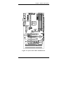
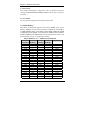
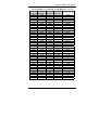
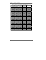
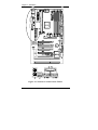
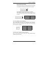
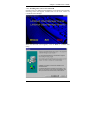
TI6NL Pentium II 440LX ATX Motherboard User's Manual Version 2.0A Contents Contents Chapter 1 Introduction.................................................... 1 Chapter 2 Specifications .................................................. 2 Chapter 3 Hardware Description ................................... 4 3.1 Processor ................................................................................... 6 3.2 L2 Cache ................................................................................... 6 3.3 Main Memory............................................................................ 6 3.4 BIOS.......................................................................................... 9 3.5 Onboard AGP Slot..................................................................... 9 3.6 Optional Winbond W83781D Hardware Monitoring IC ........... 9 3.7 Onboard Multi-I/O .................................................................. 10 3.8 Interrupt Request (IRQ) Lines ................................................. 10 3.9 Onboard PCI-IDE.................................................................... 11 3.10 DMA Channels...................................................................... 11 3.11 I/O Port Address Map............................................................ 11 Chapter 4 Configuring the Motherboard .................... 12 4.1 CPU Frequency Select: SW1(1-8)........................................... 14 4.2 Clear CMOS Select: JP7 ......................................................... 14 Chapter 5 Installation .................................................... 15 5.1 I/O Connectors ........................................................................ 17 5.2 J1: PS/2 Keyboard and PS/2 Mouse Connectors..................... 17 5.3 J2, J3: Serial Ports ................................................................... 18 5.4 J5: Parallel Port Connector...................................................... 18 5.5 J4: USB Connector.................................................................. 19 5.6 J6: Floppy Drive Connector .................................................... 19 5.7 J9: ATX Power Supply Connector .......................................... 20 5.8 J10: IrDA Connector ............................................................... 20 5.9 J16: CPU Fan Power Connector.............................................. 20 5.10 J18, J17: EIDE Connectors ................................................... 21 5.11 J19: Chassis Fan Power Connector........................................ 23 5.12 J20: Front Bezel Connectors ................................................. 23 5.13 JP2: Wake on LAN Connector .............................................. 25 5.14 JP5: CPU Voltage Testing Connector ................................... 25 5.15 JP6: SB-Link Connector........................................................ 26 TI6NL User’s Manual i Contents Chapter 6 BIOS Configuration..................................... 27 6.1 BIOS Introduction ...................................................................30 6.2 BIOS Setup ..............................................................................30 6.3 Standard CMOS Setup.............................................................32 6.4 BIOS Features Setup................................................................35 6.5 Chipset Features Setup.............................................................38 6.6 Power Management Setup .......................................................41 6.7 PNP/PCI Configuration ...........................................................44 6.8 Load BIOS Defaults ................................................................46 6.9 Load Setup Defaults.................................................................46 6.10 Integrated Peripherals ............................................................47 6.11 Supervisor / User Password ...................................................49 6.12 IDE HDD Auto Detection......................................................50 6.13 HDD Low Level Format ........................................................50 6.14 Save & Exit Setup..................................................................51 6.15 Exit Without Saving...............................................................51 Chapter 7 LANDesk User’s Guide ............................... 52 7.1 Introduction .............................................................................53 7.2 Installation ...............................................................................54 Appendix .......................................................................... 59 A. Slot 1 Retention Mechanism ......................................................59 ii TI6NL User’s Manual Chapter 1 Introduction Chapter 1 Introduction This manual is designed to give you information on the TI6NL motherboard. It is divided into the following sections: • Introduction • Specifications • Hardware Description • Configuring the Motherboard • Installation • BIOS Configuration • LANDesk User’s Guide Checklist Please check that your package is complete and contains the items below. If you discover damaged or missing items, please contact your dealer. The TI6NL Motherboard 1 IDE ribbon cable 1 floppy ribbon cable 1 CD containing Intel LANDesk or System Monitor software, PIIX4 Bus Master IDE driver and utilities, or 1 diskette containing PIIX4 Bus Master IDE driver and flash utility. Your package comes with Intel’s LANDesk or System Monitor software if your motherboard supports the onboard hardware monitoring IC. TI6NL User’s Manual 1 Chapter 2 Specifications Chapter 2 Specifications The TI6NL is a high-performance ATX 440LX motherboard with a Slot 1 connector for Pentium II processors. It offers flexibility in terms of CPU frequency and main memory type and size. The main features of the motherboard consist of the following: CPU Socket Slot 1 Processor Intel Pentium II 233/266/300/333MHz L2 Cache CPU integrated L2 cache Main Memory Four 168-pin DIMM sockets Memory types: Extended Data Output (EDO) DRAM, SDRAM (Synchronous DRAM) Memory size: 8MB, 16MB, 32MB, 64MB, 128MB Chipset Intel 82440LX with built-in PCI-IDE Super I/O Onboard super I/O is an Winbond W83977TF that provides: zTwo 16550 UART compatible serial ports zOne parallel port (ECP/EPP compatible) zOne floppy controller (2.88MB compatible) zOne IrDA port zKeyboard Controller PCI Bus Master IDE Controller (Ultra DMA/33) Onboard PCI Bus Master IDE (Ultra DMA/33) controller with two connectors for up to four IDE devices in two channels, supporting faster data transfer rates, enhanced IDE devices such as Tape Backup and CD-ROM drives, PIO Mode 3/4 and Bus Mastering Ultra DMA/33 (You have to install the Bus Master IDE driver to enable this feature.) 2 TI6NL User’s Manual Chapter 2 Specifications BIOS Award BIOS with ISA Plug and Play (PnP) extension, DMI, bootable CD-ROM and power-management features Mouse Connector PS/2 type Keyboard Connector PS/2 type USB Connector 2 ports onboard Win95-shut-off Allows shut-off control from within Windows 95 Onboard AGP Slot The AGP (Accelerated Graphics Port) slot supports AGP compliant VGA cards to achieve rich 3D and video graphics display. AGP is a platform bus specification that enables 3D graphics capabilities including support for z-buffering, alpha blending and faster texture mapping. Expansion Slots Five PCI 32-bit slots Two ISA 16-bit slots One AGP slot Form Factor ATX, 12” x 6.9” (30.5cm x 17.5cm) TI6NL User’s Manual 3 Chapter 3 Hardware Description Chapter 3 Hardware Description This chapter briefly describes each of the major features of the TI6NL motherboard. The layout of the board in Figure 1 shows the location of the key components. The topics covered in this chapter are as follows: 3.1 Processor....................................................................................6 3.2 L2 Cache....................................................................................6 3.3 Main Memory ............................................................................6 3.4 BIOS ..........................................................................................9 3.5 Onboard AGP Slot.....................................................................9 3.6 Optional Winbond W83781D Hardware Monitoring IC ...........9 3.7 Onboard Multi-I/O...................................................................10 3.8 Interrupt Request (IRQ) Lines .................................................10 3.9 Onboard PCI-IDE ....................................................................11 3.10 DMA Channels ......................................................................11 3.11 I/O Port Address Map............................................................11 4 TI6NL User’s Manual Chapter 3 Hardware Description Figure 1: Layout of the TI6NL Motherboard TI6NL User’s Manual 5 Chapter 3 Hardware Description 3.1 Processor The TI6NL motherboard is designed to take a Pentium II processor running 233MHz/266MHz/300MHz/333MHz with its Slot 1 processor connector. 3.2 L2 Cache The L2 cache is integrated in the Pentium II processor. 3.3 Main Memory The TI6NL motherboard supports four 168-pin DIMM (Dual In-line Memory Module) sockets to form a memory configuration from 8MB to 512MB. DIMM modules can be 8MB, 16MB, 32MB, 64MB and 128MB in SDRAM or EDO DRAM. In populating the DIMM sockets, DIMM1, DIMM2, DIMM3 and DIMM4 bank can be populated first. Refer to the following table on how to configure the memory. : SDRAM or EDO DRAM 168-pin DIMM (3.3V): Bank0 Bank1 Bank2 Bank3 Total Memory (DIMM4) (DIMM3) (DIMM2) (DIMM1) 8MB 16MB 32MB 64MB 128MB 8MB 16MB 32MB 64MB 128MB 8MB 8MB 16MB 32MB 64MB 128MB 8MB 16MB 32MB 64MB 128MB 6 --------------------8MB 8MB 8MB 8MB 8MB 8MB 8MB 8MB 8MB 8MB 8MB 8MB 8MB 8MB 8MB 8MB ----------------------------------------8MB 8MB 8MB 8MB 8MB 8MB 8MB 8MB 8MB 8MB 8MB ----------------------------------------------------------------8MB 8MB 8MB 8MB 8MB 8MB 16MB 32MB 64MB 128MB 16MB 24MB 40MB 72MB 136MB 24MB 24MB 32MB 48MB 80MB 144MB 32MB 40MB 56MB 88MB 152MB TI6NL User’s Manual Chapter 3 Hardware Description 168-pin DIMM (3.3V) SDRAM or EDO DRAM (continued) Bank0 Bank1 Bank2 Bank3 Total Memory (DIMM4) (DIMM3) (DIMM2) (DIMM1) 16MB 32MB 64MB 128MB 16MB 32MB 64MB 128MB 16MB 32MB 64MB 128MB 16MB 32MB 64MB 128MB 16MB 32MB 64MB 128MB 16MB 32MB 64MB 128MB 32MB 64MB 64MB 128MB 32MB 64MB 128MB 32MB 64MB 128MB 32MB 64MB 128MB 16MB 16MB 16MB 16MB 16MB 16MB 16MB 16MB 16MB 16MB 16MB 16MB 16MB 16MB 16MB 16MB 16MB 16MB 16MB 16MB 16MB 16MB 16MB 16MB 32MB 32MB 32MB 32MB 32MB 32MB 32MB 32MB 32MB 32MB 32MB 32MB 32MB TI6NL User’s Manual ----------------8MB 8MB 8MB 8MB 8MB 8MB 8MB 8MB 16MB 16MB 16MB 16MB 16MB 16MB 16MB 16MB 16MB 16MB 16MB 16MB ----------------8MB 8MB 8MB 8MB 8MB 8MB 16MB 16MB 16MB --------------------------------8MB 8MB 8MB 8MB ----------------8MB 8MB 8MB 8MB 16MB 16MB 16MB 16MB ----------------------------8MB 8MB 8MB ------------- 32MB 48MB 80MB 144MB 40MB 56MB 88MB 152MB 48MB 64MB 96MB 160MB 48MB 64MB 96MB 160MB 56MB 72MB 104MB 168MB 64MB 80MB 112MB 176MB 64MB 96MB 96MB 160MB 72MB 104MB 168MB 80MB 112MB 176MB 80MB 112MB 176MB 7 Chapter 3 Hardware Description 168-pin DIMM (3.3V) SDRAM or EDO DRAM (continued) Bank0 Bank1 Bank2 Bank3 Total Memory (DIMM4) (DIMM3) (DIMM2) (DIMM1) 32MB 64MB 128MB 32MB 64MB 128MB 32MB 64MB 128MB 64MB 128MB 64MB 128MB 64MB 128MB 64MB 128MB 64MB 128MB 64MB 128MB 64MB 128MB 64MB 128MB 64MB 128MB 128MB 128MB 8 32MB 32MB 32MB 32MB 32MB 32MB 32MB 32MB 32MB 64MB 64MB 64MB 64MB 64MB 64MB 64MB 64MB 64MB 64MB 64MB 64MB 64MB 64MB 64MB 64MB 64MB 64MB 128MB 128MB 16MB 16MB 16MB 32MB 32MB 32MB 32MB 32MB 32MB --------8MB 8MB 8MB 8MB 16MB 16MB 16MB 16MB 32MB 32MB 32MB 32MB 64MB 64MB 64MB 64MB 128MB 128MB 16MB 16MB 16MB ------------32MB 32MB 32MB ----------------8MB 8MB --------16MB 16MB --------32MB 32MB --------64MB 64MB ----128MB 96MB 128MB 192MB 96MB 128MB 192MB 128MB 160MB 224MB 128MB 192MB 136MB 200MB 144MB 208MB 144MB 208MB 160MB 224MB 160MB 224MB 192MB 256MB 192MB 256MB 256MB 320MB 384MB 512MB TI6NL User’s Manual Chapter 3 Hardware Description 3.4 BIOS The BIOS on the TI6NL motherboard provides the standard BIOS functions plus the following additional features: 1. ISA Plug and Play (PnP) Extension Unlike PCI cards that are Plug and Play, ISA cards require setting jumpers to resolve hardware conflicts. To make a computer system PnP, an ISA PnP standard is established and supported by new operating systems, such as Windows 95. Under Windows 95, the motherboard BIOS must have an ISA PnP extension to support new ISA PnP cards. 2. Power Management The power management feature provides power savings by slowing down the CPU clock, turning off the monitor screen and stopping the HDD spindle motor. The BIOS fully conforms to ACPI (Advanced Configuration and Power Interface) specification. 3.5 Onboard AGP Slot The AGP (Accelerated Graphics Port) slot supports AGP compliant VGA cards to achieve rich 3D and video graphics display. AGP is a platform bus specification that enables 3D graphics capabilities including support for z-buffering, alpha blending and faster texture mapping. 3.6 Optional Winbond W83781D Hardware Monitoring IC The W83781D is a hardware status monitoring IC that is used to monitor several hardware parameters including power supply voltages, fan speeds, and temperatures, which are very important for a high-end computer system to work stable and properly. The 48-pin LQFP-package IC is fully software compatible with Intel LDCM. TI6NL User’s Manual 9 Chapter 3 Hardware Description 3.7 Onboard Multi-I/O The onboard multi-I/O chip, W83977TF, supports a keyboard controller (AMI copyright), two serial ports, one parallel port, one floppy controller and one IrDA port. The serial ports are 16550 UART compatible. The parallel port features high-speed EPP/ECP mode. The floppy controller supports up to 2.88 MB format. 3.8 Interrupt Request (IRQ) Lines There is a total of 15 IRQ lines available on the motherboard. Peripheral devices use an interrupt request to notify the CPU for the service required. The following table shows the IRQ lines used by the devices on the motherboard: Level Function IRQ0 IRQ1 IRQ2 System Timer Output Keyboard Interrupt Cascade Real Time Clock Software Redirected to Int 0Ah Reserved Reserved Reserved Co-Processor Primary IDE Secondary IDE INTERRUPT Serial Port #1 INTERRUPT Floppy Disk Controller Parallel Port #1 IRQ8 IRQ9 IRQ10 IRQ11 IRQ12 IRQ13 IRQ14 IRQ15 IRQ3 IRQ4 IRQ5 IRQ6 IRQ7 10 TI6NL User’s Manual Chapter 3 Hardware Description 3.9 Onboard PCI-IDE The PCI-IDE controller is a part of the 82440LX PCIset. It supports PIO mode 3/4 and bus mastering Ultra DMA/33. The peak transfer rate of PIO mode 3/4 can be as high as 17MB/sec. Using HDDs that support Ultra DMA/33, the peak transfer rate can reach 33MB/sec. There are two IDE connectors - primary IDE and secondary IDE. With two devices per connector, up to four IDE devices can be supported. 3.10 DMA Channels There are seven DMA channels available on the motherboard. Only DMA2 is used by the floppy controller. In the case that ECP mode on the parallel port is utilized, DMA1 or DMA3 will be used. 3.11 I/O Port Address Map Each peripheral device in the system is assigned a set of I/O port addresses which also becomes the identity of the device. There is a total of 1K port address space available. The following table lists the I/O port addresses used on the motherboard. Address 000h - 01Fh 020h - 03Fh 040h - 05Fh 060h - 06Fh 070h - 07Fh 080h - 09Fh 0A0h - 0BFh 0C0h - 0DFh 0F0h 0F1h 1F0h - 1F7h 2F8h - 2FFh 378h - 3FFh 3F0h - 3F7h 3F8h - 3FFh TI6NL User’s Manual Device Description DMA Controller #1 Interrupt Controller #1 Timer Keyboard Controller Real Time Clock,, NMI DMA Page Register Interrupt Controller #2 DMA Controller #2 Clear Math Coprocessor Busy Signal Reset Math Coprocessor IDE Interface Serial Port #2(COM2) Parallel Port #1(LPT1) Floppy Disk Controller Serial Port #1(COM1) 11 Chapter 4 Configuring the Motherboard Chapter 4 Configuring the Motherboard The following sections describe the necessary procedures and proper jumper settings to configure the TI6NL motherboard. For the locations of the jumpers, refer to Figure 2. 4.1 CPU Frequency Select: SW1(1-8) ...........................................14 4.2 Clear CMOS Select: JP7..........................................................14 The following examples show the conventions used in this chapter. Jumper Open Jumper Closed/Short ON DIP Switch 1 and switch 2 are set to OFF. Switch 3 and switch 4 are set to ON. 1 12 2 3 4 TI6NL User’s Manual Chapter 4 Configuring the Motherboard Figure 2: Jumper Location on the TI6NL TI6NL User’s Manual 13 Chapter 4 Configuring the Motherboard 4.1 CPU Frequency Select: SW1(1-8) Refer to the following table for the correct setting to match the CPU frequency. Pentium II CPU FREQ. SW1(1-8) Switch Settings 1 2 3 4 5 6 7 8 Pentium II 233MHz off off off off on off off on 1 2 3 4 5 6 7 8 Pentium II 266MHz off off off off off on on on 1 2 3 4 5 6 7 8 Pentium II 300MHz off off off off off on off on 1 2 3 4 5 6 7 8 Pentium II 333MHz off off off off off off on on 4.2 Clear CMOS Select: JP7 Use JP7, a 3-pin header, to clear the contents of the CMOS RAM. Do not clear the CMOS RAM unless it is absolutely necessary. You will lose your password, etc. JP7 NOTE: 14 1 2 3 1 2 Jumper Setting Function pin 1-2: short Normal pin 2-3: short Clear CMOS 3 To clear CMOS, the ATX-power connector should be disconnected from the motherboard. TI6NL User’s Manual Chapter 5 Installation Chapter 5 Installation This chapter describes the interface that the TI6NL provides for creating a working system. Refer to Figure 3 for the location of the connectors. The following items are covered in this chapter: 5.1 I/O Connectors ........................................................................ 17 5.2 J1: PS/2 Keyboard and PS/2 Mouse Connectors..................... 17 5.3 J2, J3: Serial Ports ................................................................... 18 5.4 J5: Parallel Port Connector...................................................... 18 5.5 J4: USB Connector.................................................................. 19 5.6 J6: Floppy Drive Connector .................................................... 19 5.7 J9: ATX Power Supply Connector .......................................... 20 5.8 J10: IrDA Connector ............................................................... 20 5.9 J16: CPU Fan Power Connector.............................................. 20 5.10 J18, J17: EIDE Connectors ................................................... 21 5.11 J19: Chassis Fan Power Connector........................................ 23 5.12 J20: Front Bezel Connectors ................................................. 23 Speaker: Pins 1 - 4 Power LED and Keylock: Pins 11 - 15 ATX Power ON Switch: Pins 7 and 17 Turbo LED Connector: Pins 8 and 18 Reset Switch: Pins 9 and 19 Hard Disk Drive LED Connector: Pins 10 and 20 5.13 JP2: Wake on LAN Connector .............................................. 25 5.14 JP5: CPU Voltage Testing Connector ................................... 25 5.15 JP6: SB-Link Connector........................................................ 26 TI6NL User’s Manual 15 Chapter 5 Installation Figure 3: Connector Location on the TI6NL 16 TI6NL User’s Manual Chapter 5 Installation 5.1 I/O Connectors The I/O connectors connect the TI6NL to the most common peripherals. To attach cables to these connectors, carefully align Pin 1 of the cables to that of the connectors. Refer to Figure 4 for the location and orientation of the connectors. Figure 4: Orientation of the I/O Connector 5.2 J1: PS/2 Keyboard and PS/2 Mouse Connectors PS/2 Mouse PS/2 Keyboard Below are the pin-out assignments of the connectors. Signal Name Keyboard data N.C. GND 5V Keyboard clock N.C. TI6NL User’s Manual Keyboard 1 2 3 4 5 6 Mouse 1 2 3 4 5 6 Signal Name Mouse data N.C. N.C. 5V Mouse Clock N.C. 17 Chapter 5 Installation 5.3 J2, J3: Serial Ports The onboard serial ports of the TI6NL, J2 and J3, are two DB-9 external connectors. The following table shows the pin-out assignments of the these connectors. Signal Name DCD, Data carrier detect RXD, Receive data TXD, Transmit data DTR, Data terminal ready GND, ground Pin # 1 2 3 4 5 Pin # 6 7 8 9 10 Signal Name DSR, Data set ready RTS, Request to send CTS, Clear to send RI, Ring indicator Not Used J5 (Parallel Port) J2 (COM1 ) J3 (COM2) 5.4 J5: Parallel Port Connector J5 is a DB-25 external connector as seen in the above figure. The following table describes the pin- out assignments of this connector. Signal Name Line printer strobe PD0, parallel data 0 PD1, parallel data 1 PD2, parallel data 2 PD3, parallel data 3 PD4, parallel data 4 PD5, parallel data 5 PD6, parallel data 6 PD7, parallel data 7 ACK, acknowledge Busy Paper empty Select 18 Pin # 1 2 3 4 5 6 7 8 9 10 11 12 13 Pin # 14 15 16 17 18 19 20 21 22 23 24 25 N/A Signal Name AutoFeed Error Initialize Select Ground Ground Ground Ground Ground Ground Ground Ground N/A TI6NL User’s Manual Chapter 5 Installation 5.5 J4: USB Connector J4 is the standard USB external connector consisting of two ports. USB support allows connections of up to 64 plug and play external peripherals per channel. The following table shows the pin outs of these ports. Pin # 1 2 3 4 PORT2 Signal Name Vcc USBUSB+ Ground PORT1 5.6 J6: Floppy Drive Connector J6 of the TI6NL is a 34-pin header and will support up to 2.88MB floppy drives. The following table shows its pin-out assignments. Signal Name Ground Ground Ground Ground Ground Ground Ground Ground Ground Ground Ground Ground Ground Ground Ground Ground Ground TI6NL User’s Manual Pin # 1 3 5 7 9 11 13 15 17 19 21 23 25 27 29 31 33 Pin # 2 4 6 8 10 12 14 16 18 20 22 24 26 28 30 32 34 Signal Name RM/LC No connect No connect Index Motor enable 0 Drive select 1 Drive select 0 Motor enable 1 Direction Step Write data Write gate Track 00 Write protect Read data Side 1 select Diskette change 19 Chapter 5 Installation 5.7 J9: ATX Power Supply Connector J9 is a 20-pin ATX power supply connector. Refer to the following table for the pin out assignments. 11 1 20 10 Signal Name 3.3V -12V Ground PS-ON Ground Ground Ground -5V +5V +5V Pin # 11 12 13 14 15 16 17 18 19 20 Pin # 1 2 3 4 5 6 7 8 9 10 Signal Name 3.3V 3.3V Ground +5V Ground +5V Ground Power good 5VSB +12V 5.8 J10: IrDA Connector This connector is used for an IrDA connector that supports infrared wireless communication. +5V IRRX IRTX N.C. GND J10 Pin # 1 2 3 4 5 Signal Name +5V No connect Ir RX Ground Ir TX 5.9 J16: CPU Fan Power Connector J16 is a 3-pin header for the CPU fan power connector. The fan must be a 12V fan. 1 20 2 3 J16 Pin # Signal Name 1 2 3 Rotation +12V Ground TI6NL User’s Manual Chapter 5 Installation 5.10 J18, J17: EIDE Connectors J18: Primary IDE Connector Signal Name Pin # Pin # Reset IDE 1 2 Host data 7 3 4 Host data 6 5 6 Host data 5 7 8 Host data 4 9 10 Host data 3 11 12 Host data 2 13 14 Host data 1 15 16 Host data 0 17 18 Ground 19 20 DRQ0 21 22 Host IOW 23 24 Host IOR 25 26 IOCHRDY 27 28 DACK0 29 30 IRQ14 31 32 Address 1 33 34 Address 0 35 36 Chip select 0 37 38 Activity 39 40 TI6NL User’s Manual Signal Name Ground Host data 8 Host data 9 Host data 10 Host data 11 Host data 12 Host data 13 Host data 14 Host data 15 Key Ground Ground Ground Host ALE Ground No connect No connect Address 2 Chip select 1 Ground 21 Chapter 5 Installation J17: Secondary IDE Connector Signal Name Pin # Pin # Reset IDE 1 2 Host data 7 3 4 Host data 6 5 6 Host data 5 7 8 Host data 4 9 10 Host data 3 11 12 Host data 2 13 14 Host data 1 15 16 Host data 0 17 18 Ground 19 20 DRQ0 21 22 Host IOW 23 24 Host IOR 25 26 IOCHRDY 27 28 DACK1 29 30 MIRQ0 31 32 Address 1 33 34 Address 0 35 36 Chip select 0 37 38 Activity 39 40 22 Signal Name Ground Host data 8 Host data 9 Host data 10 Host data 11 Host data 12 Host data 13 Host data 14 Host data 15 Key Ground Ground Ground Host ALE Ground No connect No connect Address 2 Chip select 1 Ground TI6NL User’s Manual Chapter 5 Installation 5.11 J19: Chassis Fan Power Connector J19 is a 3-pin header for the CPU fan power connector. The fan must be a 12V fan. 1 2 3 J19 Pin # Signal Name 1 2 3 Rotation +12V Ground 5.12 J20: Front Bezel Connectors The front bezel of the case has a control panel which provides light indication of the computer activities and switches to change the computer status. J20 is a 20-pin header that provides interfaces for the following functions. Hard Disk Drive LED Reset Switch Turbo LED Connector ATX Power On Switch Not Defined Power LED and Keylock Speaker Speaker: Pins 1 - 4 This connector provides an interface to a speaker for audio tone generation. An 8-ohm speaker is recommended. J20 Pin # 1 2 3 4 TI6NL User’s Manual Signal Name Speaker out No connect Ground +5V 23 Chapter 5 Installation Power LED and Keylock: Pins 11 - 15 The power LED indicates the status of the main power switch. The keylock switch, when closed, will disable the keyboard function. J20 Pin # 11 12 13 14 15 Signal Name Power LED No connect Ground Keylock Ground ATX Power ON Switch: Pins 7 and 17 This 2-pin connector is an “ATX Power Supply On/Off Switch” on the motherboard that connects to the power switch on the case. When pressed, the power switch will force the motherboard to power on. When pressed again, it will force the motherboard to power off. Turbo LED Connector: Pins 8 and 18 There is no turbo/deturbo function on the motherboard. The Turbo LED on the control panel will always be On when attached to this connector. J20 Pin # 8 18 24 Signal Name 5V Ground TI6NL User’s Manual Chapter 5 Installation Reset Switch: Pins 9 and 19 The reset switch allows the user to reset the system without turning the main power switch Off and then On. Orientation is not required when making a connection to this header. Hard Disk Drive LED Connector: Pins 10 and 20 This connector connects to the hard drive activity LED on control panel. This LED will flash when the HDD is being accessed. J20 Pin # 10 20 Signal Name Ground 5V 5.13 JP2: Wake on LAN Connector JP2 is a 3-pin header for the Wake on LAN function on the motherboard. The following table shows the pin out assignments of this connector. Wake on LAN will function properly only with an ATX power supply with 5VSB that has 200mA. 1 2 3 JP2 Pin # 1 2 3 Signal Name +5VSB Ground Wake on LAN 5.14 JP5: CPU Voltage Testing Connector JP5 is a 10-pin connector used for testing CPU voltages. This connector should not be short/closed. TI6NL User’s Manual 25 Chapter 5 Installation 5.15 JP6: SB-Link Connector The following table shows the pin out assignments of this connector. This connector is used for the Creative Sound AWE64D PCI sound card. 26 1 2 5 6 JP6 Pin # 1 2 3 4 5 6 Signal Name GNTA# Ground No Connect REQA# Ground SERIRQ# TI6NL User’s Manual Chapter 6 BIOS Configuration Chapter 6 BIOS Configuration This chapter describes the different settings available in the Award BIOS. The topics covered in this chapter are as follows: 6.1 BIOS Introduction ................................................................... 30 6.2 BIOS Setup.............................................................................. 30 6.3 Standard CMOS Setup ............................................................ 32 Date Time Primary HDDs / Secondary HDDs Drive A / Drive B Floppy 3 Mode Support Video Halt On 6.4 BIOS Features Setup ............................................................... 35 Virus Warning CPU Internal Cache / External Cache Quick Power On Self Test Boot Sequence Swap Floppy Drive Boot Up Floppy Seek Boot Up NumLock Status Boot Up System Speed Gate A20 Option Typematic Rate Setting Typematic Rate (Chars/Sec) Typematic Delay (Msec) Security Option PCI/VGA Palette Snoop OS Select for DRAM > 64MB Video BIOS Shadow C8000 - CBFFF Shadow/DC000 - DFFFF Shadow 6.5 Chipset Features Setup ............................................................ 38 Auto Configuration DRAM Cycle Speed Selection MA Wait State CPU to PCI IDE Posting TI6NL User’s Manual 27 Chapter 6 BIOS Configuration System BIOS Cacheable Video BIOS Cacheable Video RAM Cacheable 8 Bit I/O Recovery Time 16 Bit I/O Recovery Time Memory Hole at 15MB Addr. Passive Release Delayed Transaction AGP Aperture Size (MB) SDRAM RAS-to-CAS Delay SDRAM RAS Precharge Time SDRAM CAS Latency Time CPU Warning Temperature Current CPU/Chips Block Temp. / Current System Temp. Current Chassis / CPU Fan Speed VCCP / VTT / VCC3 6.6 Power Management Setup .......................................................41 Power Management PM Control by APM Video Off Method Video Off After Modem Use IRQ Doze Mode Standby Mode Suspend Mode HDD Power Down Throttle Duty Cycle VGA Active Monitor IRQ 8 Break Suspend Soft-Off by PWR-BTTN Resume by Ring Resume by Alarm Reload Global Timer Events 6.7 PNP/PCI Configuration ...........................................................44 PNP OS Installed Resources Controlled by Reset Configuration Data IRQ3/4/5/7/9/10/11/12/14/15, DMA0/1/3/5/6/7 assigned to PCI IDE IRQ Map To Used MEM base addr 28 TI6NL User’s Manual Chapter 6 BIOS Configuration 6.8 Load BIOS Defaults ................................................................ 46 6.9 Load Setup Defaults ................................................................ 46 6.10 Integrated Peripherals............................................................ 47 IDE HDD Block Mode IDE Primary/Secondary Master/Slave PIO IDE Primary/Secondary Master/Slave UDMA On-Chip Primary/Secondary PCI IDE USB Keyboard Support Onboard FDC Controller Onboard Serial/Parallel Port UART Mode Select Parallel Port Mode 6.11 Supervisor / User Password................................................... 49 6.12 IDE HDD Auto Detection ..................................................... 50 6.13 HDD Low Level Format........................................................ 50 6.14 Save & Exit Setup ................................................................. 51 6.15 Exit Without Saving .............................................................. 51 TI6NL User’s Manual 29 Chapter 6 BIOS Configuration 6.1 BIOS Introduction The Award BIOS (Basic Input/Output System) installed in your computer system’s ROM supports Intel/Cyrix/AMD processors in a standard IBM-AT compatible I/O system. The BIOS provides critical low-level support for standard devices such as disk drives, serial and parallel ports. It also adds virus and password protection as well as special support for detailed fine-tuning of the chipset controlling the entire system. 6.2 BIOS Setup The Award BIOS provides a Setup utility program for specifying the system configurations and settings. The BIOS ROM of the system stores the Setup utility. When you turn on the computer, the Award BIOS is immediately activated. Pressing the <Del> key immediately allows you to enter the Setup utility. If you are a little bit late pressing the <Del> key, POST(Power On Self Test) will continue with its test routines, thus preventing you from invoking the Setup. If you still wish to enter Setup, restart the system by pressing the ”Reset” button or simultaneously pressing the <Ctrl>, <Alt> and <Delete> keys. You can also restart by turning the system Off and back On again. The following message will appear on the screen: Press <DEL> to Enter Setup In general, you press the arrow keys to highlight items, <Enter> to select, the <PgUp> and <PgDn> keys to change entries, <F1> for help and <Esc> to quit. When you enter the Setup utility, the Main Menu screen will appear on the screen. The Main Menu allows you to select from various setup functions and exit choices. 30 TI6NL User’s Manual Chapter 6 BIOS Configuration ROM PCI/ISA BIOS CMOS SETUP UTILITY AWARD SOFTWARE, INC. INTEGRATED PERIPHERALS STANDARD CMOS SETUP BIOS FEATURES SETUP SUPERVISOR PASSWORD CHIPSET FEATURES SETUP USER PASSWORD POWER MANAGEMENT SETUP IDE HDD AUTO DETECTION PNP/PCI CONFIGURATION HDD LOW LEVEL FORMAT LOAD BIOS DEFAULTS SAVE & EXIT SETUP LOAD SETUP DEFAULTS EXIT WITHOUT SAVING Ç È Æ Å : Select Item ESC : Quit F10 : Save & Exit Setup (Shift) F2 : Change Color Time, Date, Hard Disk Type The section below the setup items of the Main Menu displays the control keys for this menu. Another section at the bottom of the Main Menu just below the control keys section displays information on the currently highlighted item in the list. NOTE: After making and saving system changes with Setup, you find that your computer cannot boot, the Award BIOS supports an override to the CMOS settings that resets your system to its default. We strongly recommend that you avoid making any changes to the chipset defaults. These defaults have been carefully chosen by both Award and your system manufacturer to provide the absolute maximum performance and reliability. TI6NL User’s Manual 31 Chapter 6 BIOS Configuration 6.3 Standard CMOS Setup “Standard CMOS Setup” choice allows you to record some basic hardware configurations in your computer system and set the system clock and error handling. If the motherboard is already installed in a working system, you will not need to select this option. You will need to run the Standard CMOS option, however, if you change your system hardware configurations, the onboard battery fails, or the configuration stored in the CMOS memory was lost or damaged. ROM PCI/ISA BIOS STANDARD CMOS SETUP AWARD SOFTWARE, INC. Date (mm:dd:yy) : Mon, Dec 1 1996 Time (hh:mm:ss) : 00 : 00 : 00 HARD DISKS TYPE SIZE CYLS HEAD PRECOMP LANDZ SECTOR MODE Primary Master Primary Slave Auto None 0 0 0 0 0 0 0 0 0 0 0 0 Auto ----- Secondary Master None 0 0 0 0 0 0 ----- Secondary Slave None 0 0 0 0 0 0 ----- Drive A : 1.44M, 3.5in Drive B : None Floppy 3 Mode Support : Disabled Video : EGA / VGA Halt On : All Errors ESC : Quit F1 : Help Base Memory : 640K Extended Memory : 15360K Other Memory : 384K Total Memory : 16384K Item Ç È Æ Å : Select (Shift) F2 : Change Color PU / PD / + / - : Modify At the bottom of the menu are the control keys for use on this menu. If you need any help in each item field, you can press the <F1> key. It will display the relevant information to help you. The memory display at the lower right-hand side of the menu is read-only. It will adjust automatically according to the memory changed. The following describes each item of this menu. Date The date format is: Day : Month : Date : Year : Sun to Sat 1 to 12 1 to 31 1994 to 2079 To set the date, highlight the “Date” field and use the PageUp/ PageDown or +/- keys to set the current time. 32 TI6NL User’s Manual Chapter 6 BIOS Configuration Time The time format is: Hour : 00 to 23 Minute : 00 to 59 Second : 00 to 59 To set the time, highlight the “Time” field and use the <PgUp>/ <PgDn> or +/- keys to set the current time. Primary HDDs / Secondary HDDs The onboard PCI IDE connectors provide Primary and Secondary channels for connecting up to four IDE hard disks or other IDE devices. Each channel can support up to two hard disks; the first is the “Master” and the second is the “Slave”. To enter the specifications for a hard disk drive, you must select first a “Type”. There are 45 predefined types and 4 user definable types are for Enhanced IDE BIOS. Type 1 to 45 are predefined. Type “User” is user-definable. For the Primary Master/Slave as well as Secondary Master/Slave, you can select “Auto” under the TYPE and MODE fields. This will enable auto detection of your IDE drives and CD-ROM drive during POST. Press <PgUp>/<PgDn> to select a numbered hard disk type or type the number and press the <Enter> key. The hard disk will not work properly if you enter incorrect information for this field. If your hard disk drive type is not matched or listed, you can use Type User to define your own drive type manually. If you select Type User, related information is asked to be entered to the following items. Number of cylinders CYLS : Number of read/write heads HEAD : PRECOMP : Write precompensation Landing zone LANDZ : Number of sectors SECTOR : Automatically adjust according to the configuration SIZE : MODE (for IDE HDD only) : Auto Normal (HD < 528MB) Large (for MS-DOS only) LBA (HD > 528MB and supports Logical Block Addressing) TI6NL User’s Manual 33 Chapter 6 BIOS Configuration NOTE: The specifications of your drive must match with the drive table. The hard disk will not work properly if you enter incorrect information in these fields. If your hard disk drive type is not matched or listed, you can use Type User to define your own drive type manually. Drive A / Drive B These fields identify the types of floppy disk drive A or drive B that has been installed in the computer. The available specifications are: 360KB 1.2MB 720KB 1.44MB 2.88MB 5.25 in. 5.25 in. 3.5 in. 3.5 in. 3.5 in. Floppy 3 Mode Support This is the Japanese standard floppy drive. The standard stores 1.2MB in a 3.5-inch diskette. You have four options to choose: Disabled No 3 mode floppy drive installed. (default) Drive A Installed 3 mode drive at drive A. Drive B Installed 3 mode drive at drive B. Both Installed 3 mode drive at drive A and B. Video This field selects the type of video display card installed in your system. You can choose the following video display cards: EGA/VGA For EGA, VGA, SEGA, SVGA or PGA monitor adapters. (default) CGA 40 Power up in 40 column mode. CGA 80 Power up in 80 column mode. MONO For Hercules or MDA adapters. Halt On This field determines whether the system will halt if an error is detected during power up. No errors Whenever the BIOS detects a non-fatal error, the system will stop and you will be prompted. All errors The system boot will not be halted for any error that may be detected. (default) All, But Keyboard The system boot will not be halted for a keyboard error; it will stop for all other errors All, But Diskette The system boot will not be halted for a disk error; it will stop for all other errors. All, But Disk/Key The system boot will not be halted for a keyboard or disk error; it will stop for all others. 34 TI6NL User’s Manual Chapter 6 BIOS Configuration 6.4 BIOS Features Setup This section allows you to configure and improve your system and allows you to set up some system features according to your preference. ROM / PCI ISA BIOS BIOS FEATURES SETUP AWARD SOFTWARE, INC. Virus Warning : Disabled Video BIOS Shadow : Enabled CPU Internal Cache External Cache Quick Power On Self Test Boot Sequence Swap Floppy Drive Boot Up Floppy Drive Boot Up Numlock Status : Enabled : Enabled : Enabled : A, C, SCSI : Disabled : Enabled : On C8000-CBFFF Shadow CC000-CFFFF Shadow D0000-D3FFF Shadow D4000-D7FFF Shadow D8000-DBFFF Shadow DC000-DFFF Shadow : Disabled : Disabled : Disabled : Disabled : Disabled : Disabled Boot Up System Speed : High Gate A20 Option : Fast Typematic Rate Setting : Disabled Typematic Rate (chars/Sec) :6 Typematic Delay (Msec) : 250 Security Option : Setup PCI /VGA Palette Snoop : Disabled OS Select For DRAM>64MB : Non-OS2 ESC : Quit F1 : Help Ç È Æ Å : Select Item PU/PD/+/- : Modify F5 : Old Values (Shift) F2 : Color F6 : Load BIOS Defaults F7 : Load Setup Defaults Virus Warning This item protects the boot sector and partition table of your hard disk against accidental modifications. If an attempt is made, the BIOS will halt the system and display a warning message. If this occurs, you can either allow the operation to continue or run an anti-virus program to locate and remove the problem. NOTE: Many disk diagnostic programs which attempt to access the boot sector table can cause the virus warning. If you will run such a program, disable the Virus Warning feature. CPU Internal Cache / External Cache Cache memory is additional memory that is much faster than conventional DRAM (system memory). CPUs from 486-type on up contain internal cache memory, and most, but not all, modern PCs have additional (external) cache memory. When the CPU requests data, the system transfers the requested data from the main DRAM into cache memory, for even faster access by the CPU. These items allow you to enable (speed up memory access) or disable the cache function. By default, these items are Enabled. TI6NL User’s Manual 35 Chapter 6 BIOS Configuration Quick Power On Self Test This choice speeds up the Power On Self Test (POST) after you power up the system. If it is set to Enabled, BIOS will skip some items. By default, this choice is Enabled. Boot Sequence This field determines the drive that the system searches first for an operating system. The options are : A, C, SCSI D, A, SCSI SCSI, C, A C, A, SCSI E, A, SCSI C only C, CDROM, A F, A, SCSI LS/ZIP, C CDROM, C, A SCSI, A, C The default value is A, C, SCSI. Swap Floppy Drive This item allows you to determine whether to enable Swap Floppy Drive or not. When enabled, the BIOS swaps floppy drive assignments so that Drive A becomes Drive B, and Drive B becomes Drive A. By default, this field is set to Disabled. Boot Up Floppy Seek When enabled, the BIOS will seek whether or not the floppy drive installed has 40 or 80 tracks. 360K type has 40 tracks while 760K, 1.2M and 1.44M all have 80 tracks. By default, this field is set to Enabled. Boot Up NumLock Status This allows you to activate the NumLock function after you power up the system. By default, the system boots up with NumLock On. Boot Up System Speed This has no function and selects the default system speed (High). Gate A20 Option This field allows you to select how Gate A20 is worked. The Gate A20 is a device used to address memory above 1 MB. By default, this field is set to Fast. Typematic Rate Setting When disabled, continually holding down a key on your keyboard will generate only one instance. When enabled, you can set the two typematic controls listed next. By default, this field is set to Disabled. 36 TI6NL User’s Manual Chapter 6 BIOS Configuration Typematic Rate (Chars/Sec) When the typematic rate is enabled, the system registers repeated keystrokes speeds. You can select speed range from 6 to 30 characters per second. By default, this item is set to 6. Typematic Delay (Msec) When the typematic rate is enabled, this item allows you to set the time interval for displaying the first and second characters. By default, this item is set to 250msec. Security Option This field allows you to limit access to the System and Setup. The default value is Setup. When you select System, the system prompts for the User Password every time you boot up. When you select Setup, the system always boots up and prompts for the Supervisor Password only when the Setup utility is called up. PCI/VGA Palette Snoop Some non-standard VGA display cards may not show colors properly. This field allows you to set whether MPEG ISA/VESA VGA Cards can work with PCI/VGA or not. When this field is enabled, a PCI/VGA can work with a MPEG ISA/VESA VGA card. When this field is disabled, a PCI/VGA cannot work with a MPEG ISA/VESA Card. OS Select for DRAM > 64MB This option allows the system to access greater than 64MB of DRAM memory when used with OS/2 that depends on certain BIOS calls to access memory. The default setting is NON-OS/2. Video BIOS Shadow This item allows you to change the Video BIOS location from ROM to RAM. Video Shadow will increase the video speed. C8000 - CBFFF Shadow/DC000 - DFFFF Shadow Shadowing a ROM reduces the memory available between 640KB to 1024KB. These fields determine whether optional ROM will be copied to RAM or not. TI6NL User’s Manual 37 Chapter 6 BIOS Configuration 6.5 Chipset Features Setup This Setup menu controls the configuration of the motherboard chipset. ROM PCI/ISA BIOS CHIPSET FEATURES SETUP AWARD SOFTWARE INC. Auto Configuration DRAM Speed Selection MA Wait State DRAM Integrity Mode CPU To PCI IDE Posting System BIOS Cacheable Video BIOS Cacheable Video RAM Cacheable 8 Bit I/O Recovery Time 16 Bit I/O Recovery Time Memory Hole At 15MB Passive Release Delayed Transaction AGP Aperture Size (MB) SDRAM RAS-to-CAS Delay SDRAM RAS Precharge Time SDRAM CAS Latency Time : Enabled : 60ns : Slow Non-ECC Enabled : Enabled : Enabled : Disabled :4 :3 : Disabled : Enabled : Disabled : 64 : Slow : Slow 3 CPU Warning Temperature : 66°C/151°F Current CPU Block Temp. Current CPU/Chips Block Temp. Current System Temp. Current Chassis Fan Speed Current CPU Fan Speed : 41°C/ 105°F : 27°C/ 80°F : 34°C/ 93°F : 2789 RPM : 2045 RPM VCCP (V): VCC3 (V) : +12 V : -5V : 1.98 V 3.45 V 12.46 V - 5.21 V VTT (V) +5V -12 V : 1.50 V : 4.99 V : -12.54V ESC : Quit Ç È Æ Å : Select Item F1 : Help PU/PD/+/- : Modify F5 : Old Values (Shift) F2 : Color F6 : Load BIOS Defaults F7 : Load Setup Defaults Auto Configuration This field predefined values for DRAM, cache timing according to CPU type and system clock. When this field is enabled, the predefined items will become read-only. DRAM Cycle Speed Selection This field sets the DRAM cycle speed. The options are 60ns and 70ns. By default, this field is set to 60ns. MA Wait State This field sets the wait state of the memory address. The settings are Fast and Slow. By default, this field is set to Slow. CPU to PCI IDE Posting When enabled, the CPU to PCI IDE posting cycles are treated as normal I/O write transactions. The default setting is Enabled. System BIOS Cacheable When enabled, access to the system BIOS ROM addressed at F0000H-FFFFFH are cached, provided that the cache controller is disabled. 38 TI6NL User’s Manual Chapter 6 BIOS Configuration Video BIOS Cacheable When enabled, access to video BIOS addressed at C0000H to C7FFFH are cached, provided that the cache controller is disabled. Video RAM Cacheable Selecting Enabled allows caching of the video BIOS ROM at C0000h to C7FFFh, resulting in better video performance. However, if any program writes to this memory area, a memory access error may result. 8 Bit I/O Recovery Time This option specifies the length of the delay (in sysclks) inserted between consecutive 8-bit I/O operations. The settings are 1, 2, 3, 4, 5, 6, 7, or 8. The default setting is 4. 16 Bit I/O Recovery Time This option specifies the length of the delay (in sysclks) inserted between consecutive 16-bit I/O operations. The settings are 1, 2, 3, 4, 5, 6, 7, or 8. The default setting is 3. Memory Hole at 15MB Addr. In order to improve performance, certain space in memory can be reserved for ISA cards. This field allows you to reserve 15MB to 16MB memory address space to ISA expansion cards. This makes memory from 15MB and up unavailable to the system. Expansion cards can only access memory up to 16MB. By default, this field is set to Disabled. Passive Release When enabled, CPU to PCI bus accesses are allowed during passive release. Otherwise, the arbiter only accepts another PCI master access to local DRAM. Delayed Transaction The chipset has an embedded 32-bit posted write buffer to support delay transactions cycles. Select Enabled to support compliance with PCI specification version 2.1. The default setting is Disabled. AGP Aperture Size (MB) The field sets aperture size of the graphics. The aperture is a portion of the PCI memory address range dedicated for graphics memory address space. Host cycles that hit the aperture range are forwarded to the AGP without any translation. The options available are 4M, 8M, 16M, 32M, 64M, 128M and 256M. The default setting is 64M. TI6NL User’s Manual 39 Chapter 6 BIOS Configuration SDRAM RAS-to-CAS Delay This field lets you insert a timing delay between the CAS and RAS strobe signals, used when DRAM is written to, read from, or refreshed. Fast gives faster performance; and Slow gives more stable performance. The default setting is Slow. SDRAM RAS Precharge Time If an insufficient number of cycles is allowed for the RAS to accumulate its charge before DRAM refresh, the refresh may be incomplete and the DRAM may fail to retain data. Fast gives faster performance; and Slow gives more stable performance. The default setting is Slow. SDRAM CAS Latency Time When synchronous DRAM is installed, the number of clock cycles of CAS latency depends on the DRAM timing. Do not reset this field from the default value specified by the system designer. CPU Warning Temperature This field sets the threshold temperature at which an alert is sounded through the system’s speaker. The CPU temperature is monitored by the onboard thermal sensor to prevent the CPU from overheating. Current CPU/Chips Block Temp. / Current System Temp. These read-only fields reflect the functions of the optional hardware thermal sensor that monitors the chip blocks and system temperatures to ensure the system runs stable. Current Chassis / CPU Fan Speed These optional and read-only fields show the current speeds in RPM (revolution per minute) for the CPU fan and Chassis fan as monitored by the optional hardware monitoring IC. VCCP / VTT / VCC3 These optional and read-only fields show the current voltages in the voltage regulators and power supply as monitored by the optional hardware monitoring IC. 40 TI6NL User’s Manual Chapter 6 BIOS Configuration 6.6 Power Management Setup The Power Management Setup allows you to save energy of your system effectively. It will shut down the hard disk and turn off video display after a period of inactivity. ROM PCI/ISA BIOS (2A59IM29) POWER MANAGEMENT SETUP AWARD SOFTWARE, INC. Power Management PM Control by APM Video Off Method Video Off After MODEM Use IRQ Doze Mode Standby Mode Suspend Mode HDD Power Down Throttle Duty Cycle VGA Active Monitor IRQ 8 Break Suspend Soft-Off by PWR-BTTN Resume by Ring Resume by Alarm : Disabled : Yes : V/H SYNC +Blank : Standby :3 : Disabled : Disabled : Disabled : Disabled : 62.5% : Enabled : Disabled : Instant-Off : Disabled : Disabled ** Reload Global Timer Events ** IRQ3 (3-7, 9-15), NMI : Disabled Primary IDE 0 : Enabled Primary IDE 1 : Enabled Secondary IDE 0 : Disabled Secondary IDE 1 : Disabled Floppy Disk : Disabled Serial Port : Enabled Parallel Port : Disabled ESC : Quit Ç È Æ Å : Select Item F1 : Help PU/PD/+/- : Modify F5 : Old Values (Shift) F2 : Color F6 : Load BIOS Defaults F7 : Load Setup Defaults Power Management This field allows you to select the type of power saving management modes. There are fours selections for Power Management. Disabled No power management Min. Power Saving Minimum power management Max. Power Saving Maximum power management. Only available for SL CPU User Define Each of the ranges are from 1 min. to 1hr. Except for HDD Power Down which ranges from 1 min. to 15 min. (Default) NOTE: In order to enable the CPU overheat protection feature, the Power Management field should not be set to Disabled. TI6NL User’s Manual 41 Chapter 6 BIOS Configuration PM Control by APM This field allows you to use the Advanced Power Management device to enhance the Max. Power Saving mode and stop the CPU’s internal clock. If the Max. Power Saving is not enabled, this will be preset to NO. Video Off Method This field defines the Video Off features. There are three options. V/H SYNC + Blank Default setting, blank the screen and turn off vertical and horizontal scanning. DPMS Allows the BIOS to control the video display card if it supports the DPMS feature. Blank Screen This option only writes blanks to the video buffer. Video Off After As the system moves from lesser to greater power-saving modes, select the mode in which you want the monitor to blank. Modem Use IRQ This field names the interrupt request (IRQ) line assigned to the modem (if any) on your system. Activity of the selected IRQ always awakens the system. By default, the IRQ is set to 3. Doze Mode When enabled, and after the set time of system inactivity, the CPU clock will run at a slower speed while all other devices still operate at full speed. Standby Mode After the selected period of system inactivity, the fixed disk drive and the video shut off while all other devices still operate at full speed. Suspend Mode When enabled, and after the set time of system inactivity, all devices except the CPU will be shut off. HDD Power Down When enabled, and after the set time of system inactivity, the hard disk drive will be powered down while all other devices remain active. Throttle Duty Cycle When the system enters Doze mode, the CPU clock runs only part of the time. You may select the percent of time that the clock runs. 42 TI6NL User’s Manual Chapter 6 BIOS Configuration VGA Active Monitor When enabled, any video activity restarts the global timer for Standby mode. The default setting is Enabled. IRQ 8 Break Suspend You can enable or disable monitoring of IRQ8 (the Real Time Clock) so it does not awaken the system from Suspend mode. Soft-Off by PWR-BTTN This field defines the power-off mode when using an ATX power supply. The Instant-Off mode allows powering off immediately upon pressing the power button. In the Delay 4 Sec mode, the system powers off when the power button is pressed for more than four seconds or places the system in a very low-power-usage state, with only enough circuitry receiving power to detect power button activity or Resume by Ring activity (see next field) when pressed for less than 4 seconds. The default value is Instant-Off. Resume by Ring An input signal on the serial Ring Indicator (RI) line (in other words, an incoming call on the modem) awakens the system from a soft off state. Resume by Alarm This allows a computer to be turned on automatically through the timer set int he BIOS to make the system more scheduleable. By degault, this field is set to Disabled. Reload Global Timer Events When enabled, an event occurring on each listed device restarts the global timer for Standby mode. TI6NL User’s Manual 43 Chapter 6 BIOS Configuration 6.7 PNP/PCI Configuration This option configures the PCI bus system. All PCI bus systems on the system use INT#, thus all installed PCI cards must be set to this value. ROM PCI/ISA BIOS CHIPSET FEATURES SETUP AWARD SOFTWARE INC. PNP OS Installed Resources Controlled by Reset Configuration Data : No : Manual : Disabled PCI IDE IRQ Map To Primary IDE INT# Secondary IDE INT# : PCI-AUTO :A :B IRQ-3 IRQ-4 IRQ-5 IRQ-7 IRQ-9 IRQ-10 IRQ-11 IRQ-12 IRQ-14 IRQ-15 DMA-0 assigned assigned assigned assigned assigned assigned assigned assigned assigned assigned assigned to to to to to to to to to to to : Legacy ISA : Legacy ISA : PCI/ISA PnP : Legacy ISA : PCI/ISA PnP : PCI/ISA PnP : PCI/ISA PnP : PCI/ISA PnP : PCI/ISA PnP : PCI/ISA PnP : PCI/ISA PnP Used MEM base addr : N/A DMA-1 DMA-3 DMA-5 DMA-6 DMA-7 assigned assigned assigned assigned assigned to to to to to : PCI/ISA PnP : PCI/ISA PnP : PCI/ISA PnP : PCI/ISA PnP : PCI/ISA PnP ESC : Quit Ç È Å : Select Item F1 : Help PU/PD/+/- : Modify F5 : Old Values (Shift) F2 : Color F6 : Load BIOS Defaults F7 : Load Setup Defaults PNP OS Installed This field allows you to specify if the operating system installed in your system is plug and play aware. NOTE: Operating systems such as DOS, OS/2, and Windows 3.x do not use PnP Resources Controlled by This PnP BIOS can configure all of the boot and compatible devices automatically. However, this capability needs you to use a PnP operating system such as Windows 95. The default value is Manual. Reset Configuration Data This field allows you to determine whether to reset the configuration data or not. The default value is Disabled. IRQ3/4/5/7/9/10/11/12/14/15, DMA0/1/3/5/6/7 assigned to These fields allow you to determine the IRQ/DMA assigned to the ISA bus and is not available to any PCI slot. 44 TI6NL User’s Manual Chapter 6 BIOS Configuration PCI IDE IRQ Map To This field lets you select PCI IDE IRQ mapping or PC AT (ISA) interrupts. If your system does not have one or two PCI IDE connectors on the system board, select values according to the type of IDE interface(s) installed in your system (PCI or ISA). Standard ISA interrupts for IDE channels are IRQ14 for primary and IRQ15 for secondary. Used MEM base addr Select a base address for the memory area used by any peripheral that requires high memory. The default setting is N/A. TI6NL User’s Manual 45 Chapter 6 BIOS Configuration 6.8 Load BIOS Defaults This option allows you to load the troubleshooting default values permanently stored in the BIOS ROM. These default settings are non-optimal and disable all high-performance features. ROM PCI/ISA BIOS CMOS SETUP UTILITY AWARD SOFTWARE, INC. STANDARD CMOS SETUP INTEGRATED PERIPHERALS BIOS FEATURES SETUP SUPERVISOR PASSWORD CHIPSET FEATURES SETUP USER PASSWORD POWER MANAGEMENT SETUP IDE HDD AUTO DETECTION PNP/PCI CONFIGURATION HDD(Y/N)? LOW LEVELF ORMAT Load BIOS Defaults N SAVE & EXIT SETUP LOAD BIOS DEFAULTS LOAD SETUP DEFAULTS EXIT WITHOUT SAVING Ç È Æ Å : Select Item ESC : Quit F10 : Save & Exit Setup (Shift) F2 : Change Color Load BIOS Defaults except Standard CMOS Setup To load BIOS defaults value to CMOS SRAM, enter “Y”. If not, enter “N”. 6.9 Load Setup Defaults This option allows you to load the default values to your system configuration. These default settings are optimal and enable all high performance features. ROM PCI/ISA BIOS CMOS SETUP UTILITY AWARD SOFTWARE, INC. STANDARD CMOS SETUP INTEGRATED PERIPHERALS BIOS FEATURES SETUP SUPERVISOR PASSWORD CHIPSET FEATURES SETUP USER PASSWORD POWER MANAGEMENT SETUP IDE HDD AUTO DETECTION PNP/PCI CONFIGURATION HDD(Y/N)? LOW LEVEL FORMAT Load Setup Defaults N LOAD BIOS DEFAULTS SAVE & EXIT SETUP EXIT WITHOUT SAVING LOAD SETUP DEFAULTS Ç È Æ Å : Select Item ESC : Quit F10 : Save & Exit Setup (Shift) F2 : Change Color Load BIOS Defaults except Standard CMOS Setup To load SETUP defaults value to CMOS SRAM, enter “Y”. If not, enter “N”. 46 TI6NL User’s Manual Chapter 6 BIOS Configuration 6.10 Integrated Peripherals This option sets your hard disk configuration, mode and port. ROM PCI/ISA BIOS CHIPSET FEATURES SETUP AWARD SOFTWARE INC. IDE HDD Block Mode IDE Primary Master PIO IDE Primary Slave PIO IDE Secondary Master PIO IDE Secondary Slave PIO IDE Primary Master UDMA IDE Primary Slave UDMA IDE Secondary Master UDMA IDE Secondary Slave UDMA On-Chip Primary PCI IDE On-Chip Secondary PCI IDE USB Keyboard Support : Enabled : Auto : Auto : Auto : Auto : Auto : Auto : Auto Onboard FDC Controller Onboard Serial Port 1 Onboard Serial Port 2 UART Mode Select : Enabled : 3F8/IRQ4 : 2F8/IRQ3 : Normal Onboard Parallel Port Parallel Port Mode : 378/IRQ7 : SPP : Auto : Enabled : Enabled : Disabled ESC : Quit Ç È Å : Select Item F1 : Help PU/PD/+/- : Modify F5 : Old Values (Shift) F2 : Color F6 : Load BIOS Defaults F7 : Load Setup Defaults IDE HDD Block Mode This field allows your hard disk controller to use the fast block mode to transfer data to and from your hard disk drive. IDE Primary/Secondary Master/Slave PIO These fields allow your system hard disk controller to work faster. Rather than have the BIOS issue a series of commands that transfer to or from the disk drive, PIO (Programmed Input/Output) allows the BIOS to communicate with the controller and CPU directly. The system supports five modes, numbered from 0 (default) to 4, which primarily differ in timing. When Auto is selected, the BIOS will select the best available mode. IDE Primary/Secondary Master/Slave UDMA These fields allow your system to improve disk I/O throughput to 33Mb/sec with the Ultra DMA/33 feature. The options are Auto and Disabled. TI6NL User’s Manual 47 Chapter 6 BIOS Configuration On-Chip Primary/Secondary PCI IDE The integrated peripheral controller contains an IDE interface with support for two IDE channels. Select Enabled to activate each channel separately. USB Keyboard Support Select Enabled if your system contains a Universal Serial Bus (USB) controller and you have a USB keyboard. Onboard FDC Controller Select Enabled if your system has a floppy disk controller (FDC) installed on the system board and you wish to use it. If you install an add-in FDC or the system has no floppy drive, select Disabled in this field. This option allows you to select the onboard FDD port. Onboard Serial/Parallel Port These fields allow you to select the onboard serial and parallel ports and their addresses. The default value for these ports are: Serial Port 1 3F8/IRQ4 Serial Port 2 2F8/IRQ3 Parallel Port 378H/IRQ7 UART Mode Select This field determines the UART mode in your computer. The settings are Normal, IrDA and ASKIR. The default value is Normal. Parallel Port Mode This field allows you to determine parallel port mode function. SPP Normal Printer Port EPP Enhanced Parallel Port ECP Extended Capabilities Port 48 TI6NL User’s Manual Chapter 6 BIOS Configuration 6.11 Supervisor / User Password These two options set the system password. Supervisor Password sets a password that will be used to protect the system and Setup utility. User Password sets a password that will be used exclusively on the system. To specify a password, highlight the type you want and press <Enter>. The Enter Password: message prompts on the screen. Type the password, up to eight characters in length, and press <Enter>. The system confirms your password by asking you to type it again. After setting a password, the screen automatically returns to the main screen. To disable a password, just press the <Enter> key when you are prompted to enter the password. A message will confirm the password to be disabled. Once the password is disabled, the system will boot and you can enter Setup freely. ROM PCI/ISA BIOS CMOS SETUP UTILITY AWARD SOFTWARE, INC. STANDARD CMOS SETUP INTEGRATED PERIPHERALS BIOS FEATURES SETUP SUPERVISOR PASSWORD CHIPSET FEATURES SETUP USER PASSWORD POWER MANAGEMENT SETUP IDE HDD AUTO DETECTION PNP/PCI CONFIGURATION HDD LOW LEVEL FORMAT Enter Password: LOAD BIOS DEFAULTS SAVE & EXIT SETUP LOAD SETUP DEFAULTS EXIT WITHOUT SAVING Ç È Æ Å : Select Item ESC : Quit F10 : Save & Exit Setup (Shift) F2 : Change Color Change / Set / Disable Password TI6NL User’s Manual 49 Chapter 6 BIOS Configuration 6.12 IDE HDD Auto Detection This option detects the parameters of an IDE hard disk drive, and automatically enters them into the Standard CMOS Setup screen. ROM PCI/ISA BIOS STANDARD CMOS SETUP AWARD SOFTWARE, INC. HARD DISKS TYPE SIZE CYLS HEAD PRECOMP LANDZ SECTOR MODE Primary Master: Select Primary Master Option (N=SKIP) : N OPTIONS TYPE SIZE 1 (Y) 0 0 CYLS HEAD PRECOMP 0 0 0 LANDZ SECTOR MODE 0 0 NORMAL NOTE: Some OSes (like SCO-UNIX) must use ”N NORMAL” for installation ESC: SKIP Up to four IDE drives can be detected, with parameters for each appearing in sequence inside a box. To accept the displayed entries, press the “Y” key; to skip to the next drive, press the “N” key. If you accept the values, the parameters will appear listed beside the drive letter on the screen. 6.13 HDD Low Level Format This option should only be used by a professional. Low-level formatting can cause irreparable damage to your hard disk. The procedures include selecting the drive you want to low-level format, determining the bad tracks, and proceeding with pre-formatting. 50 TI6NL User’s Manual Chapter 6 BIOS Configuration 6.14 Save & Exit Setup This option allows you to determine whether to accept the modifications or not. If you type “Y”, you will quit the setup utility and save all changes into the CMOS memory. If you type “N”, you will return to Setup utility. ROM PCI/ISA BIOS CMOS SETUP UTILITY AWARD SOFTWARE, INC. STANDARD CMOS SETUP INTEGRATED PERIPHERALS BIOS FEATURES SETUP SUPERVISOR PASSWORD CHIPSET FEATURES SETUP USER PASSWORD POWER MANAGEMENT SETUP IDE HDD AUTO DETECTION PNP/PCI CONFIGURATION HDD LOW LEVEL FORMAT Save to CMOS and Exit(y/N)? N LOAD BIOS DEFAULTS SAVE & EXIT SETUP LOAD SETUP DEFAULTS EXIT WITHOUT SAVING Ç È Æ Å : Select Item ESC : Quit F10 : Save & Exit Setup (Shift) F2 : Change Color Save Data to CMOS & Exit Setup 6.15 Exit Without Saving Select this option to exit the Setup utility without saving the changes you have made in this session. Typing “Y” will quit the Setup utility without saving the modifications. Typing “N” will return you to Setup utility. ROM PCI/ISA BIOS CMOS SETUP UTILITY AWARD SOFTWARE, INC. STANDARD CMOS SETUP INTEGRATED PERIPHERALS BIOS FEATURES SETUP SUPERVISOR PASSWORD CHIPSET FEATURES SETUP USER PASSWORD POWER MANAGEMENT SETUP IDE HDD AUTO DETECTION PNP/PCI CONFIGURATION HDD(Y/N)? LOW LEVEL FORMAT Quit Without Saving N LOAD BIOS DEFAULTS SAVE & EXIT SETUP LOAD SETUP DEFAULTS EXIT WITHOUT SAVING Ç È Æ Å : Select Item ESC : Quit F10 : Save & Exit Setup (Shift) F2 : Change Color Abandon all Data & Exit Setup TI6NL User’s Manual 51 Chapter 7 LANDesk User’s Guide Chapter 7 LANDesk User’s Guide This chapter gives a brief introduction to the optional LANDesk Client Manager (LDCM) utility, as well as the installation procedures. The following items are covered in this chapter: 7.1 Introduction .............................................................................53 7.2 Installation ...............................................................................54 7.2.1 Installing the Local Version of LDCM .........................55 7.2.2 Installing the Administrative Version of LDCM...........57 LANDesk is a registered trademark of Intel Corporation. 52 TI6NL User’s Manual Chapter 7 LANDesk User’s Guide 7.1 Introduction LANDesk Client Manager (LDCM 3.1 ) provides the capability for managing components (network interface cards, memory, printers, software applications, etc.) within a PC system. It uses the Desktop Management Interface (DMI) standard established by the Desktop Management Task Force (DMTF). Manageable components can be viewed, monitored, and administrated across multiple platforms, either locally or remotely on a network. The LDCM package has been implemented in two different ways: a user (client/local) version and an administrative version (Remote Companion). The user version provides the ability to only manage the local PC. The administrative version allows a network administrator to manage the local PC and other PC nodes on the network. This means that the administrative version has the ability to gather information about remote PCs, as well as remotely controlling the PCs. The remote access is based upon granted rights by the managed client. LDCM provides the user with self-help diagnostics, including a PC health meter, local alerting of potential problems, and hardware and software inventory. Automatic polling and alerting of memory and hardware conditions and predictive failure mechanisms minimize downtime and increase effective troubleshooting. LDCM can take periodic “snapshots” of critical configuration files for easy change management and restoration when needed. To use LDCM, your computer must meet the following requirements: z Operating System: Windows 95, Windows NT 3.51, or Windows NT4.0 z Memory: about 200KB z Disk Storage Space: 3-5MB z Hardware System: a DMI BIOS is required for full LDCM functionality For network computers, the following requirements also apply: Protocols: IPX or IP (WinSock-enabled) communication protocol loaded on the client z Hardware Interfaces: a network card for communication on the network z TI6NL User’s Manual 53 Chapter 7 LANDesk User’s Guide 7.2 Installation The optional LANDesk utility that comes with the CPU card runs in Windows NT or Windows 95 operating system. Upon entering the Windows NT 4.0 or Windows 95 environment, insert the CD. Windows will autorun the installation program and show the following screen. NOTE: 54 During Setup, you will be asked to install Internet Explorer 3.02 in order to continue, or else Setup will be aborted. LDCM supports various languages and will default to English if it is unable to load ‘language.dl’.. TI6NL User’s Manual Chapter 7 LANDesk User’s Guide 7.2.1 Installing the Local Version of LDCM Double Click on ‘LANDesk Client Manager’ in the initial screen and the following screen will appear. Double click on the local version of LANDesk Client Manager. When the Welcome screen appears, click on “Next” to continue with Setup. TI6NL User’s Manual 55 Chapter 7 LANDesk User’s Guide Choose the directory location where Setup will install LANDesk Client Manager. Click “Browse” if you want to change the directory suggested. Otherwise, click “Next” to start installing LDCM. When Setup is finished, changes will have been made to the file AUTOEXEC.BAT. Restart your computer for the changes to take effect. 56 TI6NL User’s Manual Chapter 7 LANDesk User’s Guide 7.2.2 Installing the Administrative Version of LDCM After double clicking on ‘LANDesk Client Manager’ in the initial screen, select the administrative version of the LDCM and the Welcome screen below will appear. Click on “Next” to continue. The screen below allows you to install the documentation in Adobe Acrobat format and the Adobe Acrobat Reader software. Select the options you need and click on “Next” to start the installation. TI6NL User’s Manual 57 Chapter 7 LANDesk User’s Guide After LANDesk Client Manager Setup is complete, restart your computer to be able to use the LANDesk Client Manager. 58 TI6NL User’s Manual Appendix Appendix A. Slot 1 Retention Mechanism 1. To install the Slot 1 mechanism, fasten it with the four screws from underneath the motherboard. Refer to the drawing below. 2. To release the CPU module from the retention mechanism, press the two sides of the module. Refer to the drawing below. TI6NL User’s Manual 59