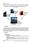
1
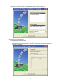
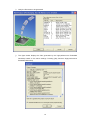
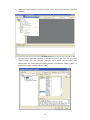
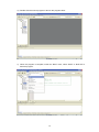
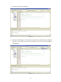
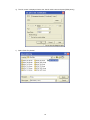
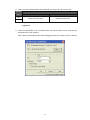
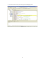
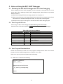
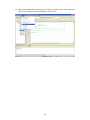
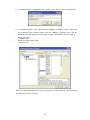
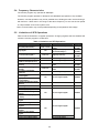
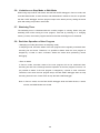
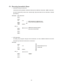
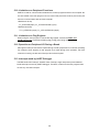
User’s Manual
16
M16C R8C UART Debugger
User’s Manual
Renesas Microcomputer Development Environment System
R8C Family / R8C/Mx Series
Notes on Connecting R8C/M11A, M12A Group
All information contained in these materials, including products and product specifications,
represents information on the product at the time of publication and is subject to change by
Renesas Electronics Corp. without notice. Please review the latest information published by
Renesas Electronics Corp. through various means, including the Renesas Technology Corp.
website (http://www.renesas.com).
www.renesas.com
Rev.1.00
Feb 2011
Notice
1.
2.
3.
4.
5.
6.
7.
All information included in this document is current as of the date this document is issued. Such information, however, is
subject to change without any prior notice. Before purchasing or using any Renesas Electronics products listed herein, please
confirm the latest product information with a Renesas Electronics sales office. Also, please pay regular and careful attention to
additional and different information to be disclosed by Renesas Electronics such as that disclosed through our website.
Renesas Electronics does not assume any liability for infringement of patents, copyrights, or other intellectual property rights
of third parties by or arising from the use of Renesas Electronics products or technical information described in this document.
No license, express, implied or otherwise, is granted hereby under any patents, copyrights or other intellectual property rights
of Renesas Electronics or others.
You should not alter, modify, copy, or otherwise misappropriate any Renesas Electronics product, whether in whole or in part.
Descriptions of circuits, software and other related information in this document are provided only to illustrate the operation of
semiconductor products and application examples. You are fully responsible for the incorporation of these circuits, software,
and information in the design of your equipment. Renesas Electronics assumes no responsibility for any losses incurred by
you or third parties arising from the use of these circuits, software, or information.
When exporting the products or technology described in this document, you should comply with the applicable export control
laws and regulations and follow the procedures required by such laws and regulations. You should not use Renesas
Electronics products or the technology described in this document for any purpose relating to military applications or use by
the military, including but not limited to the development of weapons of mass destruction. Renesas Electronics products and
technology may not be used for or incorporated into any products or systems whose manufacture, use, or sale is prohibited
under any applicable domestic or foreign laws or regulations.
Renesas Electronics has used reasonable care in preparing the information included in this document, but Renesas Electronics
does not warrant that such information is error free. Renesas Electronics assumes no liability whatsoever for any damages
incurred by you resulting from errors in or omissions from the information included herein.
Renesas Electronics products are classified according to the following three quality grades: “Standard”, “High Quality”, and
“Specific”. The recommended applications for each Renesas Electronics product depends on the product’s quality grade, as
indicated below. You must check the quality grade of each Renesas Electronics product before using it in a particular
application. You may not use any Renesas Electronics product for any application categorized as “Specific” without the prior
written consent of Renesas Electronics. Further, you may not use any Renesas Electronics product for any application for
which it is not intended without the prior written consent of Renesas Electronics. Renesas Electronics shall not be in any way
liable for any damages or losses incurred by you or third parties arising from the use of any Renesas Electronics product for an
application categorized as “Specific” or for which the product is not intended where you have failed to obtain the prior written
consent of Renesas Electronics. The quality grade of each Renesas Electronics product is “Standard” unless otherwise
expressly specified in a Renesas Electronics data sheets or data books, etc.
“Standard”:
8.
9.
10.
11.
12.
Computers; office equipment; communications equipment; test and measurement equipment; audio and visual
equipment; home electronic appliances; machine tools; personal electronic equipment; and industrial robots.
“High Quality”: Transportation equipment (automobiles, trains, ships, etc.); traffic control systems; anti-disaster systems; anticrime systems; safety equipment; and medical equipment not specifically designed for life support.
“Specific”:
Aircraft; aerospace equipment; submersible repeaters; nuclear reactor control systems; medical equipment or
systems for life support (e.g. artificial life support devices or systems), surgical implantations, or healthcare
intervention (e.g. excision, etc.), and any other applications or purposes that pose a direct threat to human life.
You should use the Renesas Electronics products described in this document within the range specified by Renesas Electronics,
especially with respect to the maximum rating, operating supply voltage range, movement power voltage range, heat radiation
characteristics, installation and other product characteristics. Renesas Electronics shall have no liability for malfunctions or
damages arising out of the use of Renesas Electronics products beyond such specified ranges.
Although Renesas Electronics endeavors to improve the quality and reliability of its products, semiconductor products have
specific characteristics such as the occurrence of failure at a certain rate and malfunctions under certain use conditions. Further,
Renesas Electronics products are not subject to radiation resistance design. Please be sure to implement safety measures to
guard them against the possibility of physical injury, and injury or damage caused by fire in the event of the failure of a
Renesas Electronics product, such as safety design for hardware and software including but not limited to redundancy, fire
control and malfunction prevention, appropriate treatment for aging degradation or any other appropriate measures. Because
the evaluation of microcomputer software alone is very difficult, please evaluate the safety of the final products or system
manufactured by you.
Please contact a Renesas Electronics sales office for details as to environmental matters such as the environmental
compatibility of each Renesas Electronics product. Please use Renesas Electronics products in compliance with all applicable
laws and regulations that regulate the inclusion or use of controlled substances, including without limitation, the EU RoHS
Directive. Renesas Electronics assumes no liability for damages or losses occurring as a result of your noncompliance with
applicable laws and regulations.
This document may not be reproduced or duplicated, in any form, in whole or in part, without prior written consent of Renesas
Electronics.
Please contact a Renesas Electronics sales office if you have any questions regarding the information contained in this
document or Renesas Electronics products, or if you have any other inquiries.
(Note 1) “Renesas Electronics” as used in this document means Renesas Electronics Corporation and also includes its majorityowned subsidiaries.
(Note 2) “Renesas Electronics product(s)” means any product developed or manufactured by or for Renesas Electronics.
Active X, Microsoft, MS-DOS, Visual Basic, Visual C++, Windows and Windows NT are either registered trademarks or
trademarks of Microsoft Corporation in the United States and other countries.
IBM and AT are registered trademarks of International Business Machines Corporation.
Intel and Pentium are registered trademarks of Intel Corporation.
Adobe and Acrobat are registered trademarks of Adobe Systems Incorporated.
All other brand and product names are trademarks, registered trademarks or service marks of their respective holders.
Keep safety first in your circuit designs!
! Renesas Technology Corporation and Renesas Solutions Corporation put the maximum effort into making
semiconductor products better and more reliable, but there is always the possibility that trouble may occur with them.
Trouble with semiconductors may lead to personal injury, fire or property damage. Remember to give due
consideration to safety when making your circuit designs, with appropriate measures such as (i) placement of
substitutive, auxiliary circuits, (ii) use of nonflammable material or (iii) prevention against any malfunction or mishap.
Notes regarding these materials
! These materials are intended as a reference to assist our customers in the selection of the Renesas Technology
product best suited to the customer's application; they do not convey any license under any intellectual property rights,
or any other rights, belonging to Renesas Technology Corporation, Renesas Solutions Corporation or a third party.
! Renesas Technology Corporation and Renesas Solutions Corporation assume no responsibility for any damage, or
infringement of any third-party's rights, originating in the use of any product data, diagrams, charts, programs,
algorithms, or circuit application examples contained in these materials.
! All information contained in these materials, including product data, diagrams, charts, programs and algorithms
represents information on products at the time of publication of these materials, and are subject to change by Renesas
Technology Corporation and Renesas Solutions Corporation without notice due to product improvements or other
reasons. It is therefore recommended that customers contact Renesas Technology Corporation, Renesas Solutions
Corporation or an authorized Renesas Technology product distributor for the latest product information before
purchasing a product listed herein. The information described here may contain technical inaccuracies or typographical
errors. Renesas Technology Corporation and Renesas Solutions Corporation assume no responsibility for any
damage, liability, or other loss rising from these inaccuracies or errors. Please also pay attention to information
published by Renesas Technology Corporation and Renesas Solutions Corporation by various means, including the
Renesas home page (http://www.renesas.com).
! When using any or all of the information contained in these materials, including product data, diagrams, charts,
programs, and algorithms, please be sure to evaluate all information as a total system before making a final decision
on the applicability of the information and products. Renesas Technology Corporation and Renesas Solutions
Corporation assume no responsibility for any damage, liability or other loss resulting from the information contained
herein.
! Renesas Technology semiconductors are not designed or manufactured for use in a device or system that is used
under circumstances in which human life is potentially at stake. Please contact Renesas Technology Corporation,
Renesas Solutions Corporation or an authorized Renesas Technology product distributor when considering the use of
a product contained herein for any specific purposes, such as apparatus or systems for transportation, vehicular,
medical, aerospace, nuclear, or undersea repeater use.
! The prior written approval of Renesas Technology Corporation and Renesas Solutions Corporation is necessary to
reprint or reproduce in whole or in part these materials.
! If these products or technologies are subject to the Japanese export control restrictions, they must be exported under a
license from the Japanese government and cannot be imported into a country other than the approved destination. Any
diversion or reexport contrary to the export control laws and regulations of Japan and/or the country of destination is
prohibited.
! Please contact Renesas Technology Corporation or Renesas Solutions Corporation for further details on these
materials or the products contained therein.
Table of Contents
1.
Connecting the Target Board to the User System......................................................... 5
2.
Preparing the M16C R8C FoUSB/UART Debugger ..................................................... 7
3.
Memory Map When Using the R8C UART Debugger................................................. 20
4.
Monitor Program Occupied Area................................................................................. 20
5.
Notes on Using the R8C UART Debugger.................................................................. 21
5.1.
Restarting the R8C UART Debugger After it is Done Debugging ................................ 21
5.2.
User Program ID Code................................................................................................. 21
5.3.
User Program Download Area ..................................................................................... 21
5.4.
Frequency Characteristics ........................................................................................... 25
5.5.
Limitations of SFR Operations ..................................................................................... 25
5.6.
Limitations on Stop Mode or Wait Mode ...................................................................... 26
5.7.
Watchdog Timer ........................................................................................................... 26
5.8.
Real-time Operation of User Program ......................................................................... 26
5.9.
Executing Anomalistic Steps ........................................................................................ 27
5.10. Limitations on Peripheral Functions ............................................................................. 28
5.11.
Limitations on Flag Register......................................................................................... 28
5.12. Operation on Peripheral I/O During a Break ................................................................ 28
5.13. Interrupts used by UART Debugger............................................................................. 28
1. Connecting the Target Board to the User System
Figure 1 Connecting the Target Board to the User System
5
Figure 2 Circuit Using the RS-232C Cable with the R8C/M11A Group.
Figure 3 Circuit Using the RS-232C Cable with the R8C/M12A Group.
6
2. Preparing the M16C R8C FoUSB/UART Debugger
The M16C R8C FoUSB/UART debugger (hereinafter R8C UART debugger) is used for
debugging by connecting an RS-232C cable between the host computer and the target
board.
A monitor program comes bundled and is automatically installed with the R8C UART
debugger software.
For the R8C Family, the monitor program is automatically programmed when starting the
R8C UART debugger. The monitor program does not need to be preprogrammed with an
M16C FlashStarter or other flash programmer.
Note: Before using the R8C UART debugger for the R8C/Mx Series, erase the user
area using a serial writer such as Flash Development Toolkit in advance.
a) To start the High-performance Embedded Workshop, go to “Start”, “Programs”,
“Renesas”, “High-performance Embedded Workshop”, and “High-performance
Embedded Workshop”. You will see the following “Welcome!” dialog box.
- “Create a new project work space”
Select this when creating a new workspace.
- “Open a recent project workspace”
Select this when using an existing workspace. Previous workspaces are displayed in the
pull-down menu.
- “Browse to another project workspace”
Select this when using an existing workspace, and there are no previous workspaces
listed in the pull-down menu.
After selecting an existing workspace and pressing [OK], the screen shown in letter t) (Page 21)
is displayed.
7
b)
Select “Create a new project workspace” and press [OK].
c) The Project Generator starts. When a toolchain is preinstalled, the following screen is
displayed.
- ”Workspace Name”
Enter a name to create a new workspace. “sample” has been input as an example.
- ”Project Name”
Enter a project name. If the project name is to be the same as the workspace name, it is
not necessary to input anything in the “Project Name” field.
8
- ” CPU family”
Select the applicable CPU family. In this case, M16C has been selected for the R8C
Family.
- ” Toolchain”
When using a toolchain, select the applicable toolchain name. When not using a
toolchain, select “None”.
- ” Project Types” Window
Select a project type. The project type which supports the C start-up has been selected
as an example.
d) Set the toolchain version.
Select “Toolchain Version”, “CPU Series”, “CPU Group” and then press [Next]. In this example,
the R8C/M12A Group is selected.
9
e) Select the MCU ROM size and other related settings.
Select the MCU ROM size and heap size. Select “None” for the on-chip debugging emulator. And
press [Next].
f)
Set the stack.
Set the “Stack Size” and press [Next].
10
g) When the toolchain setting is complete, the following screen is displayed.
Select “M16C R8C FoUSB/UART” and press [Next].
If necessary, select other targets.
h) Set the configuration file name.
Configurations are the build option settings (e.g. output of debug information or
optimization) having their own names. The term "configuration" can also be referred to
as "build configuration".
11
i)
Verify the file names to be generated.
j)
The figure below displays the files generated by the High-performance Embedded
Workshop based on the above settings. Pressing [OK] launches High-performance
Embedded Workshop.
12
k) Check the section address. Under the “Build” menu, select “Renesas M16C Standard
Toolchain”.
l)
“Renesas M16C Standard Toolchain” is displayed. Click on the “Link” tab and select
“Section Order” from the “Category” pull-down menu. Make sure the section start
address does not overlap with the monitor program occupied area shown in Table 1. If
there is any overlap, edit the address value.
13
m) Double-click the source program to launch the program editor.
n) When the program is complete, under the “Build” menu, select “Build” or “Build All” to
build the program.
14
o) The result of the build is displayed.
p) Connect with the target. A host computer can easily be connected with the target by
switching to the session file in which the setting to use the R8C UART debugger is
pre-registered.
15
q) The Init screen is displayed. Select the “Serial” radio button and press [Refer(ence)].
r)
Select “R8C-Tiny Series”.
16
s) Select one of the following MCU files depending on the group and memory size.
Memory
Group
Size
4KB
8KB
R8C/M11A
R8C/M12A
R5F2M112AUART.MCU
R5F2M122AUART.MCU
Note: 2-Kbyte memory size chips such as R5F2M110A and R5F2M120A are not
supported.
t)
Select the appropriate ”Port” and ”Baud Rate” from the pull-down menus. Press [OK] to
download the monitor program.
Note: When connecting the R8C UART debugger,all data in the flash memory is erased.
17
u) To download a user program, select “Download File (X30 file)” in the “Download
Modules” submenu under the “Debug” menu.
v) To reset the user program, select “Reset CPU” under the “Debug” menu.
18
w) The cursor moves to the top of the user program and debugging starts.
19
3. Memory Map When Using the R8C UART Debugger
Figure 4 shows a memory map (8 KB).
00000h
0FFD8h
SFR
Reserved
002FFh
Undefined
instruction
00400h
RAM
(2KB)
005FFh
Overflow
Monitor RAM
004FFh
User RAM
BRK Instruction
Address Match
Single Step
Watchdog Timer
0E000h
Reserved
User Program
Reserved
Area
Vector Area
0FFFFh
Note:
Reset
are occupied areas for the monitor program
Figure 4 Memory Map (8 KB)
4. Monitor Program Occupied Area
Table 1 Monitor Program Occupied Area
ROM / RAM
Occupied Area for Monitor Program
4KB / 384Bytes
RAM:400h to 4FFh
Vector:FFE4h to FFEFh,FFF4h to FFF7h
8KB / 512 Bytes
RAM:400h to 4FFh
Vector:FFE4h to FFEFh, FFF4h to FFF7h
20
5. Notes on Using the R8C UART Debugger
5.1. Restarting the R8C UART Debugger After it is Done Debugging
When restarting the R8C UART debugger, turn off the power to the target and turn on the
power again. When starting the R8C UART debugger again, please follow the procedure
below to connect:
(1) After disconnecting HEW with the target, please turn the power off.
(2) After turning the power of the target off again and erasing the user program area using a
serial writer such as flash Development Toolkit, turn the power of the target off.
(3) Please turn the power of the target on and start the R8C UART debugger again.
5.2. User Program ID Code
When using the R8C UART debugger, all flash memory areas are erased.
Set the ID code of the user program to all FFh when using the R8C UART debugger.
Table 2 ID Code Storing Address
Address
ID No.
Vector Table
0FFDFh to 0FFDCh
ID1
Undefined instruction
0FFE3h to 0FFE0h
ID2
Overflow
0FFE7h to 0FFE4h
BRK instruction
0FFEBh to 0FFE8h
ID3
Address match
0FFEFh to 0FFECh
ID4
Single step
0FFF3h to 0FFF0h
ID5
Watchdog timer, oscillation stop detection,
voltage monitor 2
0FFF7h to 0FFF4h
ID6
Reserved
0FFFBh to 0FFF8h
ID7
Reserved
0FFFFh to 0FFFCh
(See Note) Reset
Note: Refer to the hardware manual for the value set to address 0FFFFh.
5.3. User Program Download Area
Please note that when the area in the user program overlaps with the area in the monitor
program, the R8C UART debugger does not perform error output.
When error output is performed, please set the following:
a) Make “firm.c” and enter the following:
#include "typedefine.h"
#ifdef __UART__
#pragma section bss FirmArea
_far _UBYTE _firmarea[0xA00];
#endif
21
b) Add the file created above to the project. Under the “Project” menu, select “Add Files…”.
When the file selection screen is displayed, select “firm.c”.
22
c) To add the compile option, select “Renesas M16C Standard Toolchain…” under the
“Build” menu.
d) “Renesas M16C Standard Toolchain” is displayed. Select “Defines” from the “Show
Entries For” pull-down menu, and then press [Add…].
23
e) “Set defined macro” is displayed. Enter “_UART_” in the “Macro” field and press [OK]
f)
To set the link option, in the “Renesas M16C Standard Toolchain” window, click on the
“Link” tab and select “Section Order” from the “Category” pull-down menu. Add the
following to the start address of the monitor program occupied area shown in Table 1.
•
Memory size: 48KB
•
Memory size: 64KB, 96KB, 128KB
FirmArea_NE
FirmArea_FE
When the above settings cause the user program to overlap with the monitor program
occupied area, an error is output.
24
5.4. Frequency Characteristics
The monitor program only operates at 38600bps.
The monitor program operates in developer tool-dedicated high-speed on-chip oscillator.
However, note that operation may not be possible when dividing the main clock and using it
with less than 1 MHz even in the range of the above frequency. Do not use the low-speed
on-chip oscillator clock as the system clock.
Note: Communication may not be possible depending on temperature and voltage.
5.5. Limitations of SFR Operations
Table 3 lists the limitations of register operations. Changing registers that are disabled will
cause the monitor program to malfunction.
Table 3 Limitations on SFR Operations
Register
Default Value
Limitation
Change
Set an area not used by the monitor Partially
Reset t o 057Fh
ISP (Interrupt Stack Pointer)
program.
enabled
Writing to the D flag is ignored.
Partially
Flag Register
N/A
Do not set the D flag to 1.
enabled
Partially
Reset to 00h
Processor Mode Register 0
Single-chip mode only
enabled
Reset to 00h
Hardware Reset Protect Register
Do not change this register.
Disabled
High-Speed/Low-Speed On-Chip
Oscillator Control Register (OCOCR)
System Clock f Control Register
(SCKCR)
System Clock f Select Register
(PHISEL)
Clock Stop Control Register
(CKSTPR)
High-Speed On-Chip Oscillator
Control Register 1
High-Speed On-Chip Oscillator
Control Register 2
Oscillation Stop Detection Register
(BAKCR)
Protect Register
Port PADirection Register (PDA)
Port PARegister (PA)
Port PAMode Control Register
(PAMCR
Port 1 Function Mapping Register
1 (PMH1)
UART 0 Transmit/Receive Mode
Register
UART 0 Bit Rate Register
UART 0 Transmit/Receive Control
Register 0
UART 0 Transmit/Receive Control
Register 1
UART 0 Function Selection
Register
UART 0 Transmit Buffer Register
UART 0 Receive Buffer Register
Do not change this register.
Disabled
Please set the CPU clock to 1 MHz
or less.
Please set the CPU clock to 1 MHz
or less.
Partially
enabled
Partially
enabled
Reset to 80h
Do not change this register.
Disabled
N/A
Do not change this register.
Disabled
Reset to 00h
N/A
Enabled
N/A
N/A
Enabled
N/A
Do not change this register.
Disabled
Reset to 01h
Reset to 40h
Reset to 03h
Do not change this register.
N/A
Disabled
Do not write data to this register.
Do not read this register.
25
5.6. Limitations on Stop Mode or Wait Mode
When using stop mode or wait mode, start the R8C UART debugger in free-run mode, and
close the RAM window, C watch window, and ASM window in advance. Also, do not operate
the R8C UART debugger until the program stops at the break point by setting the break
point after exiting stop mode or wait mode.
5.7. Watchdog Timer
The watchdog timer is refreshed while the monitor program is running. When using the
watchdog timer while running the user program, note that by referring to or changing
memory content, the monitor program intervenes and the watchdog timer is refreshed.
5.8. Real-time Operation of User Program
• Sampling run mode (also known as sampling mode)
In sampling mode, execution status of the user program will be regularly monitored when
executing Go and Come. Therefore, it is possible to detect when the user program is
stopped by a break or other command. Select this mode when performing normal
debugging.
• Free run Mode
In free-run mode, execution status of the user program will not be monitored when
executing Go and Come. Although real-time operation of the user program is secure, it is
not possible to detect if the user program is stopped by a break or other command.
Therefore, even when the user program stops, the R8C UART debugger does not stop
executing Go and Come. Press STOP to stop the R8C UART debugger.
Note: In free-run mode, use the R8C UART debugger while the RAM window, C watch
window, and ASM window are closed.
26
5.9. Executing Anomalistic Steps
• Software interrupt instruction
Instructions that generate software interrupts (undefined instruction, BRK instruction,
and INT instruction) cannot be continuously step executed in the instruction internal
processing.
Example: INT instruction
NOP
NOP
INT
#3
NOP
JMP
INT instruction is skipped over
when performing step execution
MAIN
INT_3:
Address at which program
execution should stop
NOP
NOP
NOP
REIT
• INT instruction
To debug the program using the INT instruction, set the software break for the INT
instruction process and use the Go command.
Example:
NOP
INT
#3
Executed by the Go
command
NOP
JMP
MAIN
INT_3:
NOP
Break
NOP
REIT
27
5.10. Limitations on Peripheral Functions
UART0 is used for communication between the monitor program and the host computer. Do
not use UART0 in the user program. Do not connect the pins below to other pins as they are
used for communication with the host computer.
• R8C/M11A Group
P1_6/TRCIOB (9pin), P1_4/TRJO/TRCIOB (11pin)
• R8C/M12A Group
T P1_6/TRCIOB (14pin), P1_4/TRJO/TRCIOB (16pin)
5.11. Limitations on Flag Register
When using the user program to rewrite the flag register, execute the FSET and
FCLR instructions to prevent the debug flag (D flag) from being rewritten.
5.12. Operation on Peripheral I/O During a Break
Although an interrupt cannot be accepted during a break, peripheral I/O continues operating.
For example, when stopping a user program by a break during timer operation, the timer
continues counting, but the timer interrupt cannot be accepted.
5.13. Interrupts used by UART Debugger
The BRK instruction interrupt, address match interrupt, single-step interrupt and address
break interrupt are used by UART Debugger. Therefore, make sure the user program does
not use any of these interrupts.
28
M16C/R8C UART Debbuer
User’s Manual
R8C Family / R8C/3x Series, R8C/Lx Series
Notes on Connecting R8C/3xC Group R8C/3xD Group R8C/LxC Group
Publication Date:
Rev.1.00
Feb 01, 2011
Published by:
Renesas Electronics Corporation
http://www.renesas.com
SALES OFFICES
Refer to "http://www.renesas.com/" for the latest and detailed information.
Renesas Electronics America Inc.
2880 Scott Boulevard Santa Clara, CA 95050-2554, U.S.A.
Tel: +1-408-588-6000, Fax: +1-408-588-6130
Renesas Electronics Canada Limited
1101 Nicholson Road, Newmarket, Ontario L3Y 9C3, Canada
Tel: +1-905-898-5441, Fax: +1-905-898-3220
Renesas Electronics Europe Limited
Dukes Meadow, Millboard Road, Bourne End, Buckinghamshire, SL8 5FH, U.K
Tel: +44-1628-585-100, Fax: +44-1628-585-900
Renesas Electronics Europe GmbH
Arcadiastrasse 10, 40472 Düsseldorf, Germany
Tel: +49-211-65030, Fax: +49-211-6503-1327
Renesas Electronics (China) Co., Ltd.
7th Floor, Quantum Plaza, No.27 ZhiChunLu Haidian District, Beijing 100083, P.R.China
Tel: +86-10-8235-1155, Fax: +86-10-8235-7679
Renesas Electronics (Shanghai) Co., Ltd.
Unit 204, 205, AZIA Center, No.1233 Lujiazui Ring Rd., Pudong District, Shanghai 200120, China
Tel: +86-21-5877-1818, Fax: +86-21-6887-7858 / -7898
Renesas Electronics Hong Kong Limited
Unit 1601-1613, 16/F., Tower 2, Grand Century Place, 193 Prince Edward Road West, Mongkok, Kowloon, Hong Kong
Tel: +852-2886-9318, Fax: +852 2886-9022/9044
Renesas Electronics Taiwan Co., Ltd.
7F, No. 363 Fu Shing North Road Taipei, Taiwan
Tel: +886-2-8175-9600, Fax: +886 2-8175-9670
Renesas Electronics Singapore Pte. Ltd.
1 harbourFront Avenue, #06-10, keppel Bay Tower, Singapore 098632
Tel: +65-6213-0200, Fax: +65-6278-8001
Renesas Electronics Malaysia Sdn.Bhd.
Unit 906, Block B, Menara Amcorp, Amcorp Trade Centre, No. 18, Jln Persiaran Barat, 46050 Petaling Jaya, Selangor Darul Ehsan, Malaysia
Tel: +60-3-7955-9390, Fax: +60-3-7955-9510
Renesas Electronics Korea Co., Ltd.
11F., Samik Lavied' or Bldg., 720-2 Yeoksam-Dong, Kangnam-Ku, Seoul 135-080, Korea
Tel: +82-2-558-3737, Fax: +82-2-558-5141
© 2010 Renesas Electronics Corporation. All rights reserved.
Colophon 1.0
M16C R8C UART Debugger
User’s Manual
R20UT0540EJ0100
(Previous Number:REJ09B0567-0100)