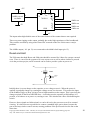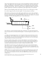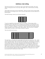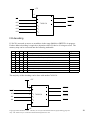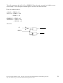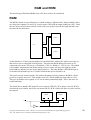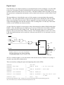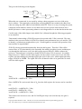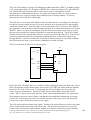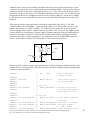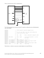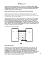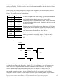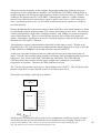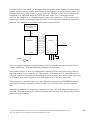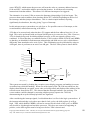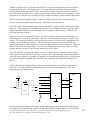
1
A-level Electronics
Major Project
Home
Automation
System
Theodore Markettos
25th March 1997
PDF conversion by GhostScript 5.10
Copyright Theo Markettos 1997. This may be used for educational and non-profit making purposes
only. The author may be reached at [email protected]
2
Contents
Summary
............................................................................1
Part 1: The microprocessor system
Choice of microprocessor ................................................3
Rest of microprocessor system ........................................5
RAM ................................................................................5
ROM ................................................................................5
Modem connection ........................................................6
Real time clock and timing ............................................6
Other inputs/outputs ........................................................7
Memory map ........................................................................8
Revisions ........................................................................9
Microprocessor control signals ........................................11
Clock................................................................................11
Reset and Halt ................................................................12
Function code outputs (FC0-FC2) ................................14
Interrupt control lines (/IPL0-/IPL2) ................................14
Bus arbitration control line (/BR, /BG, /BGACK) ............14
Asynchronous bus control signals ................................15
Address decoding ................................................................17
I/O decoding ....................................................................18
RAM and ROM ....................................................................20
RAM ................................................................................20
ROM ................................................................................22
Initial testing ........................................................................27
Digital inputs and outputs....................................................29
Digital output....................................................................29
Digital input ....................................................................32
Exception vector code ........................................................33
6800 series bus cycles ........................................................35
6800 series peripherals ........................................................38
6821 Peripheral Interface Adapter ................................38
6818 Real Time Clock ....................................................39
6522 Versatile Interface Adapter ....................................43
Serial port ............................................................................45
6850 Asynchronous Communications Interface Adapter 45
Data rate selector ............................................................45
Line drivers ....................................................................49
Interrupts ............................................................................51
Copyright Theo Markettos 1997. This may be used for educational and non-profit making purposes
only. The author may be reached at [email protected]
1
Part 2: The data link and remote module
Data link ................................................................................56
Transmission ................................................................57
Transmission filtering ....................................................62
Receiver filtering ............................................................64
Receiver amplification ....................................................66
Rethink ................................................................................67
Wire link transmitter ........................................................68
Wire link receiver ............................................................70
Amplification ....................................................................72
Signal detection ............................................................73
Data link circuit diagram ....................................................76
Remote control module........................................................78
PIC hardware ................................................................80
Remote module software ....................................................82
Main routines ................................................................83
Master control transmitter ................................................87
Master control software ....................................................91
Evaluation ............................................................................94
Photographs of project ........................................................96
The microprocessor system ............................................96
Data link and remote module ........................................100
Appendix A ............................................................................101
Appendix B ............................................................................105
Main program ................................................................105
Interrupt handling code....................................................120
Exception handling code ................................................123
Definitions file ................................................................127
Bibliography and References ............................................130
Acknowledgements ............................................................131
Copyright Theo Markettos 1997. This may be used for educational and non-profit making purposes
only. The author may be reached at [email protected]
2
Summary
The aim of this project was to build a home automation system so that the householder could dial
into their house with a modem, from the office or even the other side of the world, and control
their home appliances.
The main part of the system had to be microprocessor based, because of the requirement to
communicate intelligently with a person at the other end of a telephone line. A reasonably
powerful system was chosen to perform the task competently. This formed a flexible
multipurpose system not tied to this project. The modem input was replaced with a computer
terminal because I did not have access to two telephone lines for testing.
The main control unit talks to a module fitted in each appliance, which contains a small customprogrammed microcontroller. Originally I intended the module to communicate with the main
system over the mains wiring, but problems caused by not having direct mains access meant a
wire link had to be used instead. This was designed to be easily converted to a mains link if
required.
Overall, the system works, but the software could be substantially improved. This is a large
project, so it was not possible to refine it in the time available.
Telephone
line
Modem
Microprocessor
system
Transmission
system
Mains
wiring
forming
data
link
Appliance
to be controlled
Remote control
module
Receiving
system
Initial block diagram
The microprocessor system was split again into a number of blocks:
Copyright Theo Markettos 1997. This may be used for educational and non-profit making purposes
only. The author may be reached at [email protected]
1
AB = Address bus
CB = Control bus
DB = Data bus
Programmable
timer
EPROM
Serial interface
RAM
DB
Interrupt control
CB
AB
CB
CPU
Bus control logic &
address decoding
AB
DB
AB
DB
AB
Real time clock
DB
DB
LED display
DIP switch
Initial block diagram of microprocessor system
In the final project, these were modified slightly:
Computer
interface
to mimic
modem
Transmission
and receiving
system
Microprocessor
system
Wire
link
Appliance
to be controlled
Transmission
and receiving
system
Remote control
module
Final block diagram
Microcontroller
data link controller
To data link
6522 parallel
output and timer
Emulated EPROM
Serial interface
RAM
DB
Interrupt control
CB
AB
CB
CPU
DB
AB
Bus control logic &
address decoding
AB
DB
AB
6818 Real
Time Clock
6821 parallel
interface
DB
DB
DIP switch
LED display
Final block diagram of microprocessor system
Copyright Theo Markettos 1997. This may be used for educational and non-profit making purposes
only. The author may be reached at [email protected]
2
Choice of microprocessor
The main control unit is obviously going to require some intelligence so that it can interpret
commands sent along the phone line by modems. While it might just be possible to build a
system that used simple logic at the controller end and based the intelligence at the sending
computer, it would present its own problems. Such a system would have a program on the
transmitting computer offering options such as lights on/off/dim or heating on/off, and convert
these to codes which would then be sent along the telephone line. These codes would be in the
form that the logic at the other end could understand - for example 10 for lights, followed by a
number in the range 0 to 100 to set the intensity. The controller would receive and decode these
signals, and then perform the relevant action. This method has numerous drawbacks. Firstly, the
system is inflexible, since it can only do what is hard-wired into it. For example, it would be
very difficult to set the system to turn the heating on at 6 pm, rather than immediately. There is
also no form of error checking - the byte 10 to turn on the lights could get corrupted into 13,
which might turn the cooker on - obviously a problem. It also will only work from those
computers which have the necessary software installed, since dialling the home control system
directly will only allow communication in numeric codes.
The level of intelligence required means some form of programmable logic is required. For this
degree of complexity, it seems that a microprocessor or microcontroller is the only solution.
Other forms of programmable logic would still suffer from the problems outlined above. A
particular type and model of microprocessor/controller needs to be chosen, since, unlike NAND
gates each type is basically unique and its individual characteristics need to be taken into account
from the earliest design stages. It is very rare that one microprocessor is a ‘drop-in’ replacement
for another, and this would only happen within the same microprocessor family.
In a commercial situation, it would be likely that a microcontroller would be used. For this
project, however, this can oversimplify matters. Some microcontrollers simply require
programming of their internal EPROM or EEPROM memory, the provision of a power supply
and a few clock components, and you have a full system, including parallel and serial outputs, a
real time clock, and plenty of onboard memory, with virtually no external electronics at all. In
addition, the project needs to be assembled on solderless breadboard. This will only fit dual-inline ICs, which creates problems since most microcontrollers come in PLCC (plastic leaded chip
carrier), PGA (pin grid array) or surface mount packages, which will not fit in the board. In most
cases reliability problems may arise if an adaptor has to be made to convert these packages to a
DIL pinout.
This means a choice of microprocessor has to be made. Many of the fairly low powered
processors originated in the early 1970s and, while still available, have not been developed
recently. It is preferable if the project uses a processor which is still having new versions added
to the range, and so is not obsolete. The slower 4 and 8 bit processors also may not have enough
power to be able to handle the task easily. For example, many 8 bit computers cannot receive
data through the serial port faster than 9600 bits per second because they simply cannot keep up
with the incoming flow of data. It is certainly true that not all 8 bit microprocessors will have
this problem, as modern versions have been streamlined to work at upwards of 20 MHz.
However, these high frequencies generally cause havoc on breadboard, where the board
capacitance is quite high.
Copyright Theo Markettos 1997. This may be used for educational and non-profit making purposes
only. The author may be reached at [email protected]
3
This frequency problem is also true for 16 and 32 bit processors as well, as they are generally
designed for high power applications, which also employ high clock speeds. However, these are
generally more efficient, so that a 16 bit processor running at the same clock speed as an 8 bit
processor will be able to shift data around faster, not least because of its bigger bus size.
It would be possible to use modern, high powered RISC processors such as the ARM, SPARC,
PowerPC or MIPS systems. However, these are all 32 bit processors, so would require ROM
and RAM 32 bits wide. Using standard static RAM and EPROM chips, this would require a
total of eight 28 pins ICs just to provide storage. In addition, there is still the problem that none
of these are available in DIL packages.
This leaves 16 bit processors, of which there are two main families, the Motorola 68000 family
and the Intel 80x86 family (otherwise known as the Intel iAPX family). The simplest versions of
the 80x86 family which are available in DIL packages are the 8086, which has a 16 bit data bus,
and the 8088, with an 8 bit external data bus but a 16 bit internal data bus. This means the two
chips are identical from a software point of view, but the 8088 requires less wiring. The 68000
family is similar, with the 68000 (16 bit data bus) and 68008 (8 bit data bus) being available in
DIL packages. The Intel family have a multiplexed address and data bus, which means that
external logic is required to demultiplex them. They also have a ‘segmented architecture’, which
means that the entire memory is not available at the same time.
For these reasons, the 68000 family was chosen. This leaves a choice between the 68000 and
68008. The 8 bit bus requirement means that instruction execution times on the 68008 are
double that of the 68000, since, to access an instruction it has to perform two memory reads.
This means the power of the processor is approximately halved. For this reason the 68000 was
chosen.
Due to the nature of a microprocessor system, a large amount of hardware has to be in place
before anything can work, but once this basic hardware is present, new sections can be tested as
they are added on.
Copyright Theo Markettos 1997. This may be used for educational and non-profit making purposes
only. The author may be reached at [email protected]
4
Rest of microprocessor system
Having decided to use the 68000 microprocessor, decisions now need to be made on the
peripherals that will be attached to it. It is best to decide on this from the start, so that they can
be taken into account when other parts of the system are designed.
RAM
The system needs some RAM to store data that it is working on. There are two main types of
high density RAM used in computer systems - static and dynamic RAM. Static RAM holds the
data in arrays of flip-flops, while dynamic RAM uses large numbers of capacitors. The problem
with these capacitors is that their charge leaks across the dielectric, so needs to be refreshed
every few milliseconds. DRAMs also have a multiplexed address bus, in which the row and
column addresses of the capacitor matrix are strobed in sequentially. This means the access
cycle is very complicated, with critical timing requirements. Not only does this require a lot of
logic to generate the required cycle, but also the large currents drawn and fast signals mean that
noise is a real problem, especially on the high capacitance breadboard. This is why most modern
production computer systems have the RAM mounted on a four or six layer PCB. It would be
possible to utilise ready made memory cards, such as SIMMs, but the problems with timing
would still remain.
By contrast, SRAMs are reasonably easy to use, they don’t have a multiplexed address bus, so
have no major timing problems. They are also available with an 8 bit wide data bus, which
means that only two RAM ICs are required for the 68000‘s 16 bit data bus. Looking through a
supplier’s catalogue, shows that there is not a huge choice of suitable devices for breadboard
mounting. There are a large number of very fast (~20ns) chips, which are designed as external
cache RAM for advanced microprocessors, but their surface mount packages mean they will not
fit on breadboard. There are three possible sizes of SRAM: 8 Kbyte, 32 Kbyte, and 128 Kbyte.
Since two chips are required, it seems that 32K or 128K devices would be excessive, and there is
a large price difference between them and the 8K devices. It was therefore decided to use two
8K 6264 chips to give 16K of RAM.
ROM
A ROM is required to store the main program code. The initial thought for ROM would be to
use EPROM (Erasable Programmable Read Only Memory), which can be programmed in a
special programmer, and can be erased by exposure to 257.3nm ultraviolet light for about 20
minutes. The EPROM is then inserted into the microprocessor system breadboard, and the
program can then run. The delay means that every time the program is modified, there is a 20
minute wait before it can be tested. This is obviously not ideal.
An alternative is EEPROM (Electrically Erasable Programmable ROM), which can be erased in
a few seconds with a voltage applied to it. This is better, but these devices are expensive, and
require removal from the breadboard to be programmed.
In the commercial market, EPROM emulators are available, which consist of a box which plugs
into the socket where an EPROM would go, and connects to a computer. The box holds a static
RAM, which can be programmed by the computer and appears to be an EPROM from the
microprocessor’s point of view. These are very expensive, and here two would be required.
Copyright Theo Markettos 1997. This may be used for educational and non-profit making purposes
only. The author may be reached at [email protected]
5
However, since the microprocessor system is being designed from scratch, an EPROM emulator
can be built on breadboard, to which the address, data and control buses can connect it to the rest
of the system.
The ROM system therefore requires a size of static RAM to be chosen. Because of the price
difference, 8K devices were again chosen to give 16K of ROM. Since they are mostly pin
compatible, they can be replaced with 32K devices if required.
Modem connection
Modems invariably communicate with a microprocessor system using a serial link, as this is the
way the information will be sent through the telephone system. The parallel-based
microprocessor system needs some form of converting parallel data to a serial signal and back
again. This could be done with discrete logic, but the asynchronous nature of the RS232 serial
communications used presents problems. It is much easier to use a dedicated LSI IC to perform
the conversion, and they often have extra features such as error detection as well. There are a
large number of these devices available, many of which are designed for particular
microprocessor architectures. Those that are not generally require great care to ensure read and
write cycles are compatible with the 68000. The 68000 family has its own array of serial
controllers, such as the 68562 dual universal serial communications controller, or the 68681 dual
universal asynchronous receiver/transmitter. While these are designed to interface with the
68000‘s bus, they are expensive and complex. An alternative is to look to the 6800 family,
which were the 8 bit predecessors of the 68000. The 68000 can drive 6800 series peripherals, by
modifying its bus cycle and effectively accessing the bus at 1 MHz instead of 8 MHz. This gives
a performance decrease, but when the maximum data rate modems can handle is 28800 bits per
second, this should not be a problem. The 6850 ACIA (asynchronous communications interface
adapter) would be seem to fit this application, and they are cheap and widely available.
Real time clock and timing
The system needs an accurate way of telling the time, so that commands to activate appliances at
a particular time can be accepted. It would be possible to derive such a signal from the
microprocessor clock, but a hardware system consisting of dividers would not be flexible
enough, and a software based system could not keep the time to a reasonable standard of
accuracy. However, dedicated ICs are available for this purpose, mainly to keep the time and
date in desktop PCs. Of the field available, a look through a supplier’s catalogue shows that
most are quite expensive. One that is not is the 146818, which is a CMOS part and also happens
to be a member of the Motorola 6800 family, and therefore this was chosen. Once I had received
the data sheet, I found out that this uses a multiplexed address and data bus. With this device,
the address is placed on the bus and then address strobe (AS) taken high. AS is then negated,
and then the data read or written in conjunction with data strobe (DS) and read-write (R-/W).
While the 68000 has pins with these labels, they do not perform the same function as those on
the 6818, and it cannot multiplex its bus. The 6818 therefore cannot be connected directly.
The data sheet gives two possible alternatives for interfacing with a non-multiplexed bus. One is
to use the bus control signals of the processor with some combinational logic to simulate a
multiplexed bus cycle by writing to the device twice. An example is not shown for the 68000,
and this method seems quite risky because it is very difficult to troubleshoot it if it does not
work. The alternative given is for a single chip microcomputer, and involves simply connecting
Copyright Theo Markettos 1997. This may be used for educational and non-profit making purposes
only. The author may be reached at [email protected]
6
the address/data bus to one input/output port, and the control signals to another. This seems a
more reasonable situation, where the processor can control the bus signals directly, which is a
simpler situation to debug.
This requires another device to provide the link between clock chip and processor. Sticking to
the simple and cheap 6800 family, the 6821 provides two 8-bit bidirectional ports, which would
be enough to handle the 11 signals from the 6818.
In addition to the real time clock, which is updated once a second, it is useful to have a fast
timer, for purposes such as serial input/output, frequency measuring, etc. The 6840
Programmable Timer Module is a flexible timer chip which performs this function. It contains
three 16-bit counters which count at up to 8 MHz with many different control settings.
Other inputs/outputs
A port is required so that the system can communicate with other devices in the house. This will
require only a few bidirectional lines, so could be provided by the spare lines on the 6821.
For the purposes of testing, it is useful to have a simple set of inputs and outputs, such as a bank
of switches and LED display. To aid their simplicity, it is best if these are made from standard
TTL components. These don’t require any complicated control signals and are much faster than
the more flexible LSI devices.
Copyright Theo Markettos 1997. This may be used for educational and non-profit making purposes
only. The author may be reached at [email protected]
7
Memory map
From this information a map showing which devices are allocated to which memory addresses is
required. Since the 68000 series uses memory mapped I/O, this includes all I/O devices as well
as ROM and RAM. At the start of the project, a provisional memory map was drawn up:
Base address
$FFFFFF
Empty Address Space
$0C0000
Repetition of I/O block 127 times
$080800
Unused
$080700
Digital Outputs
$080600
Digital Inputs
$080500
Input/Output area
6818 Real Time Clock
$080400
6840 Programmable Timer Module
$080300
6800 series peripheral space (Unused)
$080200
6850 serial port 2
$080100
6850 serial port 1
$080000
Up to 240K extra RAM
$084000
RAM area
16K installed RAM
$040000
Up to 240K extra ROM
$044000
16K installed ROM
ROM area
$000400
68000 exception vectors
$000000
Note: $ is used to denote a hexadecimal number
Copyright Theo Markettos 1997. This may be used for educational and non-profit making purposes
only. The author may be reached at [email protected]
8
The choice of up to 256K of each of ROM, RAM and Input/Output (I/O) space is deliberate,
giving a total address space requirement of 768K, which will fit into the 1Mb address space of
the 48-pin 68008. This is so that the same software could be used on a system based around
either the 68000 or the 68008 with little or no modification. I/O does not really need 256K of
space, but an equal allocation to each sector saves on address decoding logic.
ROM has to be present at location $000000 and upwards since the 68000 reads the address to
jump to on a reset from an address table stored in the first 1K of memory, from $000 to $3FF.
The 16K of ROM therefore extends from $000000 to $00003FFF. To allow more ROM to be
fitted easily, an empty space is left between $004000 and $040000, where up to 240K of
additional ROM can be fitted.
RAM is therefore fitted from location $40000 to $43FFF. There is nothing that specifies where
RAM has to be since only the ROM contains references to it, which can be changed. Again this
can be expanded to 256K if required.
Likewise, there is no specific reason why I/O is placed in a chunk from $80000 to $C0000. The
I/O space is split into a number of sub-sections, each of which is allocated to an individual chip.
The figure of 256 bytes per device is, for the most part, excessive, but allows the same allocation
for each one, again saving on logic. The space is deliberately organised, so that the first four
devices require a synchronous VPA/VMA access (which will be dealt with later), while the
higher four can be accessed using normal bus cycles. This means that when I/O is selected, the
state of address line 10 (A10) signifies which type of access is required (low for VPA, high for
asynchronous).
Revisions
The memory map was later revised for a number of reasons. Firstly, it was decided that a second
serial port would be unnecessary, since more complicated programming would be required to
drive both simultaneously. The space in the memory map is left free so that another can be
installed if required, but this is overkill for this project. After receiving the 6818‘s data sheet, the
6821 had to be inserted between the 6818 and the processor to simulate a multiplexed bus. This
also provides a few spare general purpose digital input/output lines.
The decision was taken to replace the 6840 with a 6522 Versatile Interface Adapter (VIA), which
performs most of its timing functions, but has the advantage of two 8-bit input/output ports.
These ports provide more lines to communicate with the other devices in the house, and are more
flexible than using the spare lines from the 6821. This uses the same bus protocol as the 6800
series, but is from Rockwell instead of Motorola.
The digital out and digital in are wasting a block of address space, since they only work if
written to or read from respectively. These were combined onto one address, $80600, so that a
read examines the input, while a write outputs data.
The 6850 which drives the serial port has a very limited way of selecting transmit and receive
rates, which does not allow all those data rates which could be output by a modem or computer.
It therefore needs some external circuitry to select the data rate under processor control. Since
the 6850 occupies two addresses, the external circuitry should be in this area ($80000 to
$800FF), but clear of these two addresses. The simplest way is for the 6850 to be at $80000 and
$80002, and the data rate selector to be above this at $80004. The reason why these addresses go
Copyright Theo Markettos 1997. This may be used for educational and non-profit making purposes
only. The author may be reached at [email protected]
9
up by two instead of one is that the 68000 is a 16-bit processor but each address is treated as 8
bits, so $80000 refers to the top half of the data bus (D8-D15) and $80001 to the bottom half
(D0-D7). It is simpler to connect only one half of the data bus to the 8-bit bus of the 6850 and
refer to it as the consecutive 16-bit addresses $80000 and $80002 than try to mess around with
multiplexing, connecting the top half of the bus to the chip when $80000 is accessed and the
bottom half when $80001 is accessed. Thus the register select line of the 6850 is connected to
A1.
The revised memory map is as follows:
Base address in hex
FFFFFF
Empty Address Space
0C0000
Repetition of I/O block 127 times
080800
Unused
080700
Digital Inputs/Outputs
080600
Unused
080500
Input/Output area
Unused
080400
6522 Versatile Interface Adapter
080300
6821 Peripheral Interface Adapter
080200
080100
080004
080000
Unused
Serial data rate selector
6850 serial port 1
Up to 240K extra RAM
084000
RAM area
16K installed RAM
040000
Up to 240K extra ROM
044000
16K installed ROM
ROM area
000400
68000 exception vectors
000000
Copyright Theo Markettos 1997. This may be used for educational and non-profit making purposes
only. The author may be reached at [email protected]
10
Microprocessor control signals
As well as the two major address and data buses, the microprocessor has a number of control
signals which need to connected in the correct way before it will work. Most of these are dealt
with below. A full list is given in Appendix A figure 3-1.
Note: The terms assertion and negation have been used here to avoid confusion between active
low and active high signals. They state whether a signal is active or not independently of
whether it is represented by a high or low voltage. / is used to denote an active low signal, as in
/DTACK, which is also referred to by its proper notation, DTACK , where possible.
Clock
The device in use is an MC68000P8, which means it is rated at 8 MHz. According to the 68000
User’s Manual, this means it can be clocked with a single phase clock between 4 and 8 MHz.
Since the project is being built on breadboard, it is advisable to choose the lowest possible
frequency, as the high capacitance of breadboard may cause significant problems with high
frequency signals. For this reason, 4 MHz seems the optimum frequency. The 68000 uses
dynamic registers, so a lower frequency would mean that there is the possibility of them being
corrupted.
This 4 MHz has to derived from some sort of oscillator. This could be a simple RC oscillator,
but the frequency of this is not precise, and will drift with temperature. This prevents it being
used for precise timing. An alternative is to use a crystal based system. Due to the problems
found using an external circuit to drive a discrete crystal in the previous project, it seems better
to avoid them and use a crystal oscillator which is guaranteed to work.
The problem with using a crystal oscillator directly is that they produce a waveform which is not
necessarily square, and does not have a 50:50 mark:space ratio. This is vitally important in a
microprocessor system, where the clock may be split up within the processor into different
phases. The simplest way to overcome this is to feed the clock into a divider, so that an even
square wave it produced as long as the clock period is constant, which it is from a crystal
oscillator. This requires an oscillator of twice the desired frequency. To allow an 8 MHz signal
to be used if required, a 16 MHz oscillator was chosen.
This has to be fed into a divider, which can be any binary counter. The 74LS161 happened to be
to hand, which is a 4 bit synchronous counter. The synchronous nature means that race hazards
will not occur, and the 4 bits mean that 8, 4, 2 and 1 MHz frequencies can be produced. It was
connected as follows:
Copyright Theo Markettos 1997. This may be used for educational and non-profit making purposes
only. The author may be reached at [email protected]
11
+5V
+5V
14
16
1
16MHz crystal
oscillator
8
2
7
0V
7
MR V
CEP
9
CC
CP
PE
74LS161 CET 10
Q
0 14
Q
1 13
Q
2
Q 12
GND
3 11
8
0V
8MHz out
4MHz out
2MHz out
1MHz out
The inputs taken high disable some of the extra features of the counter that are not required.
There was some ringing on the output, probably due to the high capacitance of the breadboard.
This could be rectified by using some form of RC network on the line if this causes a major
problem.
The 4 MHz output (‘161 pin 13) was connected to the 68000 clock input (pin 15).
Reset and Halt
The UM states that both /Reset and /Halt pins should be asserted for 100ms for a proper external
reset. There is a need for the system to be reset at power on as well as when a button is pressed.
As in the previous project, an RC network can be used to provide a pulse at power on.
5V
C
220nF
Vout
R
1M
0V
Initially there is no net charge on the capacitor, so no voltage across it. When the power is
applied, it gradually charges up, causing the voltage across it to increase. This causes the input
to the Schmitt Trigger to drop, giving a low-to-high transition on the output. This is precisely the
change required on the Reset and Halt lines. A switch across the capacitor will discharge it if
pressed, so it behaves as at power on, causing a reset. This also has the effect of debouncing the
switch.
However, these signals are bidirectional, so can be driven by the processor as well as external
circuitry. It is therefore not a good idea to connect a standard logic gate to them, because the
gate will always sink or source current, causing problems if the processor drives the line at the
same time.
Copyright Theo Markettos 1997. This may be used for educational and non-profit making purposes
only. The author may be reached at [email protected]
12
The alternative is to use tristate or open-collector drivers, which will behave as an open circuit if
they are not enabled. Open-collector drivers only have the ability to pull the line low, while
tristates can pull it high or low without external resistors.
Tristates were therefore chosen because they have more flexibility, so the spare gates in a tristate
chip do more than the spare gates in a open-collector driver chip.
The RC network was connected to tristates to perform the reset as shown below.
5V
220nF
RESET
HALT
1M
0V
It is also useful if the reset button could toggle the reset state, so that one press starts a reset, and
the next allows the processor to start execution. Many forms of bistable could be used for this
operation, but the simplest from a design point of view is to use a D flip-flop with /Q connected
to D. On each successive rising clock edge, the output will change state. A D flip flop, on a
74LS74A, was connected in this way between the Schmitt Trigger and the tristates:
5V
220nF
D
S
Q
X
1M
R
Q
RESET
HALT
0V
Unfortunately, this prevents the power-on reset from working! As a coincidence, the RC network
before the flip-flop now performs the function of debouncing the reset switch. The simplest way
of overcoming this is to use another RC network and Schmitt Trigger, which is ORed with the
output of the flip-flop.
The wired-OR feature of /Reset and /Halt can also be used, very simply, by using another switch
to pull /Halt low to temporarily freeze the system. Debounce is not really required because the
halt function in any case is a cumbersome way of stopping the system. This could be added if it
was required.
Copyright Theo Markettos 1997. This may be used for educational and non-profit making purposes
only. The author may be reached at [email protected]
13
Indicators were put on both /Reset and /Halt to show their current state. Since both these lines
are open-drain, when not asserted they are floating. Pull-up resistors were put on them to
prevent any noise affecting their state:
+5V
10K
10K
RESET
HALT
0V
Function code outputs (FC0-FC2)
These three outputs show the function the processor is currently performing (supervisor or user
mode, program or data access). In a more complex system they could be used to protect
privileged areas of memory or expand the address space, but here they will just be taken to LEDs
via buffers to show their state.
Interrupt control lines (/IPL0-/IPL2)
These signal to the processor if an interrupt is asserted. Interrupts will be ignored for the
moment until the rest of the system is working, so they will just be taken high.
Bus arbitration control line (/BR, /BG, /BGACK)
These lines allow other devices to control the address, data and control buses, for example in
multiprocessor systems. This is a very basic system, so they are not needed. They could be used
in the EPROM emulator system, except that for another device to access the buses, the
cooperation of the processor is required. If the processor has crashed due, say, to a corrupt
program, it may not be possible to access the bus to correct that program. To disable them, input
/BR and /BGACK are taken high.
Copyright Theo Markettos 1997. This may be used for educational and non-profit making purposes
only. The author may be reached at [email protected]
14
Asynchronous bus control signals
Inputs: Bus error (/BERR) and data acknowledge (/DTACK)
Outputs: Address strobe (/AS), read/write (R-/W), and upper and lower data strobes (/UDS
and /LDS respectively)
These signals control the flow of data on the buses. A condensed version of the many pages of
timing diagrams in the User’s Manual is as follows:
Read Cycle:
1
R-/W set high (read), function code outputs show type of access (see above)
2
Address placed on address lines
3
Address strobe (/AS) asserted to show the address is valid
4
Data strobes asserted as required (/UDS shows data is required on D8-D15, /LDS shows
data is required on D0-D7 of data bus)
5
The processor then waits for /DTACK to be asserted, which signals the receiver has put the
data on the data lines.
6
Processor stores the data and negates the bus control signals
A write cycle is similar except that data is flowing in the opposite direction, so it is up to the
device being written to find out when the data is valid and latch it. It should assert /DTACK to
say it has done so.
Unfortunately, none of the RAM being used has any form of acknowledge signal, so this twoway ‘conversation’ cannot take place. This is also true of most TTL logic, and microprocessor
support devices not designed specifically for the 68000 bus. The /DTACK signal is required
because otherwise the processor will wait forever for a non-existent acknowledge signal.
An alternative is to wait a long enough period of time until the device being accessed will have
responded, and then assert /DTACK. This destroys the two-way nature of the system, as the
processor has no way of knowing whether the data has been transferred successfully, but it is the
only simple way of making the system work.
The initial thought for a delay circuit is one using RC decay such as the one below:
Signal in
Signal out
0V
Copyright Theo Markettos 1997. This may be used for educational and non-profit making purposes
only. The author may be reached at [email protected]
15
This was investigated for the previous project, and it was found that it would not respond to fast
signals. The signals here are slower than those involved when the RC circuit was tested, but it
still may be unpredictable. An alternative would be to use a digital delay line which will delay
the signal by a precise time. These are expensive, and are overkill since all that is required is to
produce a pulse after a certain time, not reproduce an entire signal exactly as it was entered.
With a bit of lateral thinking, another idea emerged. This was to use a shift register as a delay
line, which is triggered by the relevant bus signals. The basic principle is as follows.
When the bus is not being accessed, the shift register is held in reset. Once a bus cycle begins,
the reset is released, and ones begin clocking through under control of the system clock. One of
the outputs of the shift register is designated DTACK, so that when a one reaches it, it is inverted
and triggers /DTACK, thus ending the bus cycle. This is shown below:
+5V
AS
2
1
A
System clock
B
Reset
8
Q
Q
5
74LS164
9
7
11
13
BERR
DTACK
The 74LS164 is a serial-in parallel-out shift register with master reset which suits this purpose.
It has two inputs which are internally ANDed together. If connected together, they behave as one
input.
According to the timing diagram above, the /AS signal is the first asserted (taken low) when a
bus cycle begins. The ‘164 has an active low master reset, which is the reverse of the state on
/AS. Therefore /AS needs to be inverted and then taken to the master reset of the shift register,
which will enable it as soon as a bus cycle starts.
Bearing in mind the timing problems involved with breadboard, it was decided to make the
processor perform a large number of ‘wait-states’ for each bus cycle by not asserting /DTACK
for some time, thereby slowing the whole system down and increasing reliability. This gets
around the limitation that the processor cannot be reliably clocked below 4 MHz.
Thus DTACK was taken from Q5 of the shift register and inverted to form /DTACK which is
taken to the processor. In actual fact, /DTACK is an open collector input so that more than one
device can assert it at once. This could be implemented with a tristate as with /RESET but, since
only one signal drives it, there is little point in this.
/BERR is the bus error signal which alerts the processor that something has gone wrong on the
bus. This can be conveniently connected to Q7 of the shift register, so that if /DTACK is, for
some reason, not asserted then two clock cycles later /BERR will prevent the processor from
waiting forever.
Copyright Theo Markettos 1997. This may be used for educational and non-profit making purposes
only. The author may be reached at [email protected]
16
Address decoding
The memory map has to be converted into a logic system which will accept the value on the
address bus and generate the relevant chip enable signals. This is called the address decoding
circuit.
The decoding can be split up into two main chunks. Firstly, the system needs to decide whether
ROM, RAM or I/O is being accessed. If I/O is accessed, it then needs to work out which device
should respond.
The initial decoding is shown by the following truth table:
A19
0
0
A18
0
1
Function
ROM
RAM
1
1
0
1
I/O
Empty
To provide compatibility with the 68008, A20-A23 are ignored. This decoding could be
performed by discrete logic gates, but it is simpler to use a dedicated 1 of 4 decoder chip. The
74LS139 contains two of these, but since the other half of the chip would remain idle, it seems
better to use a 74LS138, which is a 1 of 8 decoder. If A20 is used as the most significant input,
another four address areas of 256K each are made available. These would not be compatible
with the 68008, but could be used for further expansion if required.
Thus the truth table now becomes:
A20
0
A19
0
A18
0
Function
ROM
Signal name
/ROMCS
0
0
0
0
1
1
1
0
1
RAM
/RAMCS
I/O
/IOCS
Reserved for further expansion
1
x
x
Reserved for further expansion
The signal names are the names the output signals will be known by from now on. The ‘138 has
active low outputs, but this does not matter since most chips have a combination of active high
and low chip select inputs. Those not required can be taken to the relevant supply rail. The ’138
is also useful because it has two active low and one active high enable input. If these are not
activated, all the outputs are held high, disabling all devices. According to the 68000 User’s
Manual, the /AS output is asserted to signify the address is valid. Therefore this needs to be
taken to an active low input, so that the devices are not enabled when the address bus is changing
state, which could lead to spurious chip selects being produced. Address line A23 also needs to
be low, as when high it signifies an interrupt acknowledge cycle is in progress (more on this
later), and the above allocations do not take it high.
Copyright Theo Markettos 1997. This may be used for educational and non-profit making purposes
only. The author may be reached at [email protected]
17
+5V
6
5
AS
4
A23
3
A20
2
A19
1
E
E
E
74LS138
A
0
ROMCS
1
RAMCS
2
2
IOCS
A
1
A
A18
0
I/O decoding
If /IOCS is asserted, an access to an address in the range $80000 to $BFFFF is in progress.
Further address decoding is required to determine which I/O device is being accessed. The
memory map can be converted into the following truth table:
A10
0
0
A9
0
0
A8
0
0
A2
0
1
Function
Serial port ACIA
Serial data rate (bits per second) select
Signal name
/ACIACS
/SERBPSCS
0
0
0
0
1
1
1
0
1
x
x
x
Space for second serial port (not fitted)
6821 Peripheral Interface Adapter (PIA) - 6818 clock interface /PIACS
6522 Versatile Interface Adapter (VIA)
/VIACS
1
1
1
0
0
1
0
1
0
x
x
x
Unused
Unused
Digital Input/Output
1
1
1
x
Unused
/DIOCS
The majority of this decoding can be done with another 74LS138.
+5V
6
4
IOCS
A10
A9
3
2
1
E
E
A
2
A
SERCS
2
PIACS
3
VIACS
6
DIOCS
1
A
A8
74LS138
0
0
E
0V
Copyright Theo Markettos 1997. This may be used for educational and non-profit making purposes
only. The author may be reached at [email protected]
18
This will not generate the /ACIACS or /SERBPSCS lines, but only a general serial address space
access output. This will require external logic to convert it into these two lines.
From the truth table above:
ACIACS = SERCS • /A2
/ACIACS = /(SERCS • /A2)
= /SERCS + A2
SERBPSCS = SERCS • A2
/SERBPSCS = /(SERCS • A2)
= /SERCS + /A2
Therefore:
A2
SERBPSCS
SERCS
ACIACS
Copyright Theo Markettos 1997. This may be used for educational and non-profit making purposes
only. The author may be reached at [email protected]
19
RAM and ROM
The interfacing of RAM and ROM to the CPU now needs to be considered.
RAM
The RAM is based on two 6264 devices, which each have eight data lines, thirteen address lines,
two chip select signals (CS and /CS), a write strobe (/WE) and an output enable pin (/OE). Since
the two devices need to form a block 16 bits wide, one needs to provide the high data lines and
the other the low data lines:
D15
D8
RAM1
D15
CPU
Data bus
D0
D7
RAM2
D0
As the data bus is 16 bits wide but addresses each hold 8 bits, address line A0 does not exist, as
this refers to one or other half of the data bus. Therefore the RAM address lines have to be
connected to the next CPU line up i.e RAM:A0 - CPU:A1, RAM:A1 - CPU:A2 etc. The 68000
is big-endian, which means that when storing a 2 byte word it will store the high byte at the
lower address, and the low byte at the address above it. Therefore RAM1 will hold the byte at
00, RAM2 will hold the byte at 01, RAM1 will hold the byte at 02 and so on.
This just leaves the control signals. The address decoding circuitry produces /RAMCS, which
goes low to signify an access. This matches with /CE, which enables the chip when it is low.
There are no further select signals, so CE can be taken permanently high. This is the same for
both RAM chips.
The initial idea to handle /WE and /OE was to connect /WE to R-/W, so that a write (R-/W low)
activates the write enable, and /OE to an inverted R-/W, /R-W, which will allow a read to activate
the outputs.
RAM1
WE
OE
RAM2
WE
OE
R-W
Copyright Theo Markettos 1997. This may be used for educational and non-profit making purposes
only. The author may be reached at [email protected]
20
Unfortunately, a problem emerged because the data strobes /UDS and /LDS are not involved in
this. Therefore if a write is performed, the RAM may latch the data before it has become valid.
Therefore an improvement needs to be made in this circuit to accommodate /UDS and /LDS. A
general data strobe (/DS) was then generated by logically ORing the two signals together, and
this fed into a series of gates to provide /WE and /OE.
DS = LDS + UDS
/DS = /(LDS + UDS)
/DS = /LDS • /UDS
OE = R-/W • DS
/OE = /(R-/W • DS)
/OE = /R-W + /DS
WE = /R-W • DS
/WE = /(/R-W • DS)
/WE = R-/W + /DS
RAM1
WE
UDS
LDS
RAM2
WE
OE
OE
DS
R-W
This does ensure the data is valid before it is written. However, a glance through the 68000
User’s Manual showed that if a byte is written to the memory, the rest of the data bus will
contain invalid data. With the current system, that invalid data will be stored in the RAM
alongside the correct data on the other half of the data bus.
This is the only cycle that causes problems. A byte read is fine because the CPU will ignore the
unwanted half of the data bus.
Therefore, the /WE needs to be separate for each RAM chip. The 68000 uses the /UDS and
/LDS lines to signal which half of the data bus is being accessed, or if both are being used
simultaneously, in a word read or write operation. /OE can be as before since the unwanted half
of the data bus is ignored during a byte read cycle.
UWE = upper data write enable
UWE = UDS • /R-W
/UWE = /(UDS • /R-W)
/UWE = /UDS + R-/W
LWE = lower data write enable
LWE = LDS • /R-W
/LWE = /(LDS • /R-W)
/LWE = /UDS + R-/W
RAM1
WE
OE
RAM2
WE
OE
R-W
UDS
LDS
DS
Copyright Theo Markettos 1997. This may be used for educational and non-profit making purposes
only. The author may be reached at [email protected]
21
ROM
The ROM in this system is composed of two 6264 static RAM chips which can be read and
written to by the programming computer, but only read by the microprocessor system. Since the
6264 has only one data bus and one address bus, some logic is needed to decided what is
accessing it and connect the accessing address and data buses to the RAM chip. It would be
possible to use dual-ported RAM, which has two separate address and data buses, but this is
expensive, and it is unnecessary since there in no need to program the RAM while the processor
is running a program stored in it. This would, in most cases, confuse the processor and cause it
to crash. The block diagram of the arrangement is shown below:
Tristates
Upper data bus
Tristates
RAM
To computer
Tristates
Address bus
Tristates
To CPU
RAM
Tristates
Lower data bus
Tristates
Some thought also needs to be put into how the system will connect to the computer. To ensure
compatibility with as many models of computer as possible, it is best to use a standard interface.
The two common interfaces are serial and parallel ports. In this case, the parallel port seems
more useful, since its parallel outputs can drive directly the parallel data and address buses. The
serial port would require an additional serial to parallel converter, which for an RS232 serial link
is quite complex. This leaves the problem that the parallel port provides 5 digital inputs, 3
digital outputs, and 9 bidirectional digital lines, all of which can be independently controlled.
This needs to be converted to 16 data lines, 13 address lines, the chip select pin and the write
enable input. Since there are only 12 output lines on the port, it is not possible to write a full 16
bits at a time, so each chip has to be accessed individually. It would also be an advantage if the
computer could read back the values it has written to the RAM, to check that they are correct.
This means the tristates between the computer and the RAM’s data bus need to be bidirectional.
Since this section is acting as a ROM, it is better that the tristates between the RAM chip and the
CPU data bus are unidirectional, so the processor is unable to corrupt the contents of the RAM
chip. The address lines are only inputs to the RAM, so only need unidirectional tristates in either
direction.
Copyright Theo Markettos 1997. This may be used for educational and non-profit making purposes
only. The author may be reached at [email protected]
22
The limit of 12 outputs means that the address and data lines of each ROM chip cannot be
controlled simultaneously, so multiplexing is required. It is therefore necessary to latch the
address lines and then hold them steady while the data is read or written from the RAM. This is
shown in the diagram below (only one RAM chip shown):
To computer
Latch
Tristates
Address bus
Tristates
Latch
To CPU
RAM
Tristates
Lower data bus
Tristates
There are a large number of possible logic devices which could perform the functions in the
above diagram. Two which appear suited to this situation are the 74LS245 ‘octal bus
transceiver’, which is basically two sets of eight tristates pointing in opposite directions,
controlled by direction and enable pins, and the 74LS373 ‘octal transparent latch with 3-state
outputs’, which combines the latch and tristates on the address bus into a single chip. As the
CPU side can drive all the address and data lines simultaneously, no latches are required.
Therefore standard octal tristates can be used. The 74LS244 ‘octal buffer with 3-state outputs’
performs this function and was to hand, so was used. This has two active low enable inputs, one
for each of four tristates. All the tristates used here have Schmitt Trigger inputs, which improves
their noise immunity.
These chips take up 8 of the 9 bidirectional parallel port pins. This leaves 4 possible outputs to
select the relevant tristates and enable the RAM. One pin needs to be a direction, and so control
the write enable lines and the bidirectional tristate direction input. The four tristate chips
controlled by the computer each need to be accessed in turn. This requires further multiplexing.
A counter could be used, but this would require a strict sequence of accessing to be followed.
Two output lines can be converted to four by passing them through a one-of-four decoder to
activate a device based on the binary code of the inputs. The 74LS139 does this, producing
active low outputs. The latches have active high clock inputs and active low output enable
inputs. In this application, the 74LS139 needs to be connected to their clock, so that to store data
on them, it is written onto the parallel data lines, and the 139 activated to clock this onto the
latches. The 74LS139 has an active low enable input, which takes all outputs high when it is
deactivated. This switches off the computer side of the interface and allows the CPU to access
the RAM. Another parallel port output is required to drive this, and to enable the latches’ outputs
to feed the address onto the ROM address bus. The remaining 1 output line can become a ROM
select line, which is asserted when the computer wants to access the RAM chips, and enables
everything associated with the computer interface.
Copyright Theo Markettos 1997. This may be used for educational and non-profit making purposes
only. The author may be reached at [email protected]
23
Since the ROM select line coming out of the CPU‘s address decoding is active low, as is the
output enable line on the RAM chip, the computer’s ROM select should also be active low. If
they were active high, the two select lines could be ORed together to produce a single OE input
to the RAM. However, they are active low, so an AND is required:
OE = CS1 + CS2
/OE = /(CS1+CS2)
/OE = /CS1 • /CS2
This leaves a problem. Only one RAM chip can be accessed at a time. For computer read cycles
this does not matter, as half of the data bus outputs are ignored. However, for write operations,
only half of the data is valid, as only one set of data bus tristates are enabled. With a common
write line, one RAM chip will store invalid data. This could be got around simply by using
another parallel port output line. However, all the possible outputs are in use.
When the computer is writing to the RAM, it enables one or other 74LS245, which feeds the data
on the data bus into the relevant RAM chip. The 74LS245 is selected by an enable line from the
74LS139, which is controlled by two parallel port outputs. This can be used to route the write
enable line to the RAM chip connected through to the data lines.
UWE = upper RAM chip write enable
U245E = upper 74LS245 enable
CWE = computer write enable output
UWE = U245E • CWE
/UWE = /(U245E • CWE)
/UWE = /U245E + /CWE
This is similar with the low RAM chip. /U245E is linked to the 245 in the active low form, so no
inversion is required for it. The RAM chip needs an active low write strobe, which fits in with
/UWE. This means the active high output from the computer has to be inverted to produce
/CWE. It would be possible to adjust the programming software to pull CWE low to activate it,
but due to the layout of the circuit on breadboard, it was more convenient to connect the RAM to
the B side of the 74LS245s and the computer to the A side. Therefore to do a write the DIR pin,
which is driven from the computer’s write enable output, should be taken high to transmit data
from A to B. This is the reverse of what the RAM requires, so an inverter will be required
somewhere. This is an arbitrary decision, but it was decided to make CWE active low, as all the
other signals in the system are also active low. Therefore /CWE needs to be inverted when
connected to the direction input on the 74LS245s.
Combining all these elements produces the circuit below:
Copyright Theo Markettos 1997. This may be used for educational and non-profit making purposes
only. The author may be reached at [email protected]
24
Parallel
printer
port
signals
SELECT IN
ERROR
STROBE
CWE
1
3
O
2
O
A0 A1
O
0
74LS139
O
E
AUTO FEED
D0-D7
D0-D7
D0-D7
D0-D7
D0-D7
A
DIR
E
LE
B
Q
74LS245
D
OE
Q
74LS373
OE
D
E
B
74LS373
LE
A
74LS245
DIR
ROMCTRL
D8-D15
A8-A12
A0-A7
D0-D7
A0-A12
WE
D0-7
6264
OE
CE
CE
OE
A0-A12
A0-A12
6264
WE
D0-D7
D12-15
D8-D11
A12
A8-A11
A4-A7
A0-A3
D4-D7
D0-D3
1G 2G
1A
1Y
1Y
2Y
74LS244
2A
1A
74LS244
2A
2Y
1G 2G
1Y
1G 2G
1A
2Y
74LS244
2A
1Y
1G 2G
1A
2Y
74LS244
2A
D12-D15
D8-D11
A12
A8-A11
A4-A7
A0-A3
D4-D7
D0-D3
D8-D15
D0-D7
A8-A12
A0-A7
D0-D7
D0-D15
A0-A12
CPU data bus
CPU address
bus
ROMCS
25
Copyright Theo Markettos 1997. This may be used for educational and non-profit making purposes
only. The author may be reached at [email protected]
This section was tested by connecting it to a computer and then reading and writing data between
the RAM and computer using the parallel port. The RAM did work, but this only tests the
computer side of it. As a very basic test of the CPU side, the address lines were hardwired into a
pattern, and /ROMCS asserted. A logic probe was then used to examine the output which would
go onto the CPU data if it were connected. This showed it worked. However, I noticed that if
both the computer was writing when the CPU was reading, the address lines of each would both
drive the RAM data bus, so the contents of the RAM would become corrupted. The fault was
indicated by ANDing /ROMCS and /ROMCTRL, which produces a low output if either is low:
CLASH = ROMCS + ROMCTRL
/CLASH = /(ROMCS + ROMCTRL)
/CLASH = /ROMCS • /ROMCTRL
The LED was connected between the AND gate output and +5V, so that it illuminates if a clash
occurs:
+5V
ROMCS
ROMCTRL
The memory corruption was prevented by using logic to disable the 74LS244s when the
computer is accessing the RAM:
/ROMCS /ROMCTRL 244 /ENABLE
0
0
1
0
1
1
1
0
1
0
1
1
From this it can be seen the /244E = /ROMCTRL • ROMCS. An AND gate was therefore used:
Four 74LS244s
1G
2G
1G
2G
ROMCTRL
ROMCS
Copyright Theo Markettos 1997. This may be used for educational and non-profit making purposes
only. The author may be reached at [email protected]
26
Initial testing
Now that a fair proportion of the hardware was in place, basic testing could take place to see if
there was anything seriously wrong.
The first test consisted of filling pages 0-3 ($000 to $3FF) with $FFFFFFFF. These pages hold
all the exception vectors, each of which points to a routine that the processor jumps to if it
detects an error, which Motorola calls an exception. When reset, the processor reads the
supervisor stack pointer from $0 and the address of the code to call on reset from $4. In this case
both are $FFFFFFFF, which are out of range addresses, so will trigger an address error, which
involves it jumping to the address held at $C. Since this also contains $FFFFFFFF, an invalid
address, the processor will go into ‘double bus fault’ mode, which means it will assert /Halt and
then stop.
When the program was run by releasing the reset button, the Reset LED was off, Halt was on,
and the function code LEDs showed 110, which fits in with the above process. This provides
one piece of evidence that the system is working.
The next test involved setting all the exception vectors to $00000400, a valid address in ROM.
$0, the supervisor stack pointer, was set to $42000, an address in the middle of RAM. This now
allows the processor to run code from $400 when it is reset. The instruction STOP was loaded at
$400. When run, this program turned off both the Reset and Halt LEDs, and set the function
code LEDs to 101. These can be interpreted as shown in Appendix A figure 3-3. A 101 state
shows that the processor is not fetching instructions, so is stopped.
A slightly longer program was assembled and loaded at $400:
00000400
00000400 4E71
00000402 60FC
00000404
1
2
3
4
loop
ORG $400
NOP
BRA.S loop
This is an endless loop that does nothing. When run, Reset and Halt were off, and the function
code LEDs showed 111. This relates to a CPU space cycle, which should happen very rarely.
When examined with an oscilloscope, it was found that both FC0 and FC1 were rapidly
changing state, which would show up as a dim LED. This seems to suggest that the program is
alternating between supervisor data and program accesses.
All the tests so far would not show if any errors were occurring, since, if an error occurred, the
processor would examine the relevant exception vector and jump straight back to the start of the
code at $400. To see if any errors were occurring, the address exception vector was set to
$FFFFFFFF. The other vectors were then overwritten one by one with $FFFFFFFF, and the
program tested after each one. The idea behind this is that if an error occurs, the program will
examine the relevant exception vector, find it to contain an invalid address, and so cause an
Address Error. Since the Address Error vector also contains an invalid address, the processor
stops with a double bus fault as before. By overwriting the exception vectors one by one, it is
possible to work out which exception vector, if any, is being triggered.
Copyright Theo Markettos 1997. This may be used for educational and non-profit making purposes
only. The author may be reached at [email protected]
27
When this was done, it was found that the processor was calling the Illegal Instruction vector.
By modifying the program at $400, it was possible to determine that the processor objected to bit
14 being set in $60FC, the BRA.S loop instruction. This suggests a problem with the high data
bus. The data bus from the ROM 74LS244s to the processor was examined, and it was found
that bit 14 was connected to bit 10 by mistake, so the processor was reading the instruction as
$00FC, which is an illegal instruction.
Having rectified this fault, another simple program was tried. This now goes into user mode by
clearing status register bit 13, and then goes into an endless loop. If it works without any
exception vectors being called, the supervisor LED, which is connected to FC2, should stay
extinguished.
00000400
00000400 46FC 0000
00000404 4E71
00000406 60FC
1
2
3 loop
4
ORG $400
MOVE.W #0,SR
NOP
BRA.S loop
This did happen, proving the system was working.
Copyright Theo Markettos 1997. This may be used for educational and non-profit making purposes
only. The author may be reached at [email protected]
28
Digital inputs and outputs
Having now got the main microprocessor system working, its inputs and outputs can now be
considered. The simplest of these are the digital output (connected to a bank of LEDs) and the
digital input (connect to a bank of DIP switches).
Digital output
This output is to drive a bank of LEDs as a general purpose output port. Since the 68000’s data
bus is 16 bits wide, it is useful to have a 16 bit wide display, so that any number which can be
represented on the data bus can be shown on the display. As the 68000 uses /LDS and /UDS to
signify which data lines are valid, the display can also be treated as two independent 8 bit
displays.
To do this requires a latch, which will hold the data steady when it is not being written to. The
address decoding circuitry needs to be arranged to clock this latch when the output port is being
written to, which will transfer the data value from the data bus onto the outputs. For each half to
be accessible individually, each eight bits needs a separate clock signal. Since there are no 16-bit
latch chips available, two 8-bit latches will have to be used instead. The device must have an
asynchronous reset, so that it will come into a known state when the system is powered up,
otherwise it could inadvertently switch on devices connected to the outputs such as heaters or
alarm systems.
There is only one widely available device that fits this specification, the 74LS273. This is a
D-register, not a latch, which means that it is edge, not level, triggered. In this situation this is an
advantage, because when the latch is first triggered the valid data may not have reached it, due to
propagation delays through other components. A D-register can be triggered on the edge when
the chip enable signal is negated, which allows ample time for the data to be valid. According to
the 68000 User’s Manual, there is 40ns between /UDS and /LDS being negated and the data
becoming invalid. The ‘FAST and LS TTL data book’ says that 74LS273 needs the data to be
stable for 5ns after it has been clocked, so this will work.
Taking the high data bus D-register (bits D8-D15), the register needs to be clocked when UDS is
high, DIOCS is high and R-/W is low:
CLK = UDS • DIOCS • /R-W
/CLK = /(UDS • DIOCS • /R-W)
/CLK = /UDS + /DIOCS + R-/W
/UDS, /DIOCS, and R-/W are the signals actually available from the CPU and address decoding.
In the above equation, CLK will go low only if all three conditions are satisfied. As soon as one
is released, CLK will go high. This is shown by the following timing diagram:
Copyright Theo Markettos 1997. This may be used for educational and non-profit making purposes
only. The author may be reached at [email protected]
29
DIOCS
(from AS and A1-A23)
R-/W
UDS
Data
Valid
CLK (allowing for
propagation delays)
The register is rising edge triggered, so triggers on the rising edge of /CLK. Thus the register
will be clocked with valid data.
The Boolean expression describes the following logic system:
DIOCS
R-W
CLK
74LS273
UDS
2-input OR gates have to be used because these are the only type available in the 74 series or its
variants. For the low data bus the system would be the same, except using /LDS instead of
/UDS. Since the top OR gate is common to both, its output can be shared between each system.
The final circuit constructed was as below:
Copyright Theo Markettos 1997. This may be used for educational and non-profit making purposes
only. The author may be reached at [email protected]
30
D8-D15
D
Q
330 Ω
DIOCS
For
all 8
bits
R-W
CLK
74LS273
0V
MR
UDS
RESET
MR
CLK
LDS
D0-D7
D
Q
330 Ω
For
all 8
bits
0V
This was tested with the following program which performs a binary count on the LEDs:
00000400
00000400
00000404
00000404
00000406
00000406
00000408
0000040E
46FC 0000
7000
5240
33C0 00080600
223C 0000FFFF
1
ORG $400
2
MOVE.W #0,SR
3 main
4
MOVEQ #0,D0
5 main_loop
6
ADDQ.W #1,D0
7
MOVE.W D0,$80600
8
MOVE.L #$FFFF,D1
00000414
00000414 51C9 FFFE
9 delay_loop
10
DBF
00000418
00000418 60EC
11
12
* Go into user mode
* Clear D0
* Increment D0
* Output D0 to all LEDs
* Amount of time to
waste
D1,delay_loop * Decrement D0, waste
time if not zero
BRA.S main_loop
* loop round
This shows that the LEDs were working by displaying a binary count on them. From the order
they were being illuminated, it could be seen that some of the data connections were wrong.
After examination, it was found that lines D0-D4 were twisted so that LED 0 was connected to
D4, LED 1 to D3 and so on. Once this was fixed, the LEDs displayed a proper count. By
changing the pin of the 74LS161 that the master clock was connected to, it was possible to see
the effect of different clock speeds. All from 8 to 1 MHz worked, although 1 and 2 MHz may
not be very reliable, or work on all 68000 chips.
Copyright Theo Markettos 1997. This may be used for educational and non-profit making purposes
only. The author may be reached at [email protected]
31
Digital input
Now that there is an output to display it on, the digital inputs can be considered. It was decided
to have an 8-bit input port which would initially be connected to a bank of DIP switches, but
could be connected to other devices if necessary. The bank of DIP switches are handy for giving
the system basic configuration information, such as initial serial data rate or which mode to start
up in.
The input hardware is basically the same as for the outputs except operating in the opposite
direction. Since the signals will be present from the input sources whether the CPU is reading
them or not, latching is not necessary. What is required is a tristate to buffer the inputs and
connect them through to the data bus when the CPU is reading them. For this any 8 bit tristate
will do, so the 74LS244 was chosen as before.
As only 8 bits are required, it seems neater to have them mapped to address $80600 rather than
$80601. Since the 68000 stores the high byte of a two byte word at the lower address, $80600
refers to data lines D8 to D15 during a read. Therefore the tristates have to be connected to
D8-D15, and are activated when /UDS is asserted. The 74LS244 enables are active low, so the
LED chip enable hardware can be used here, with an inverted R-/W, so it is activated on a read
not a write:
DIOCS
R-W
R-W
1G
+5V
2G
UDS
74LS244
For
all 8
bits
D8-D15
A
Y
D8-D11 connect to 1A1-1A4 of 74LS244
D12-D15 connect to 2A1-2A4 of 74LS244
Corresponding input is 1Y1-1Y4, 2Y1-2Y4
3K3
0V
/R-W is a common signal, so, since the fanout of the inverter used (a 74LS04) is very large, it
can drive any other device that needs it.
This was tested by reading the inputs and outputting them on the LEDs:
00000400
00000400
00000404
00000404
0000040C
0000040C
00000412
46FC 0000
33FC 0000 00080600
1039 00080600
13C0 00080600
00000418 60F2
1
ORG $400
2
MOVE.W #0,SR
* Go into user mode
3 main
4
MOVE.W #0,$80600 * Blank LEDs
5 loop
6
MOVE.B $80600,D0
7
MOVE.B D0,$80600 * Copy DIP switch value
to LEDs
8
BRA.S
loop
Copyright Theo Markettos 1997. This may be used for educational and non-profit making purposes
only. The author may be reached at [email protected]
32
Exception vector code
Now the LEDs are working, the handling of exceptions can be improved. Currently, they just
cause the program to restart if an exception occurs, which is not ideal. It is better to have some
display that an exception occurs. This could be achieved by displaying the vector number, plus a
recognisable flashing sequence of some kind to indicate that an exception occurred.
The main problem with this is how to load the vector number into a register. When an exception
occurs, the CPU loads the address stored at the exception vector, and jumps to it. When it has
done the jump, there is no record of which exception occurred. If all the exception vectors
pointed to the same address, it would not be possible to work out what type of exception was
detected.
Therefore, each exception vector must point to a separate routine to load the number into a
register. The neatest solution would be to have a long series of ADD instructions, so that the
relevant number were executed, adding the exception vector number onto a data register. The
problem is that there is no way of setting the register to zero in the first place.
The simplest way, therefore, is for each exception vector to point to a separate routine that loads
a register with the number of the exception, and then jumps to a main routine. This is what was
done:
Copyright Theo Markettos 1997. This may be used for educational and non-profit making purposes
only. The author may be reached at [email protected]
33
Address:
8
C
10
7C
108
10A
10C
10E
110
112
17C
17E
DC.L
DC.L
DC.L
...
DC.L
$108
$10C
$110
MOVEQ
BRA.S
MOVEQ
BRA.S
MOVEQ
BRA.S
...
MOVEQ
BRA.S
#$8,D0
exception
#$C,D0
exception
#$10,D0
exception
$17C
* code to set D0 to exception
* vector number as pointed to above
#$7C,D0
exception
exception
180
MOVE.B D0,$80600
186
MOVE.B #-1,D0
excep_loop
18A
MOVE.B D0,$80601
190
NOT
D0
192
MOVE.W #$FFFF,D1
excep_time_loop
196
DBF
19A
BRA.S
* exception vector table
* - all point to routine to set
* D0 to vector number
D1,excep_time_loop
excep_loop
* write exception code on high LEDs
* initial value to store on low LEDs
* (turn all on)
* store on low LEDs
* invert D0
* loop variable
* decrement and loop (waste time)
This stores the exception code on the high LEDs and flashes all the low LEDs in unison. The
only way out of this is to reset the processor. This did work, and running a program when this
was in place showed that no exceptions were occurring. An exception was caused by taking one
of the IPL lines low, causing an interrupt. This showed as an address error, as there was no
interrupt hardware present, but showed the exception code was working.
Copyright Theo Markettos 1997. This may be used for educational and non-profit making purposes
only. The author may be reached at [email protected]
34
6800 series bus cycles
Apart from the digital I/O, all the other inputs and outputs are serviced by 6800 series peripheral
ICs. These predate the 68000. and require the 68000 to modify its bus cycle to access them. The
basic access cycle is detailed below:
1
2
3
4
5
6
Processor starts a normal read or write cycle
External hardware asserts Valid Peripheral Address (/VPA)
Processor wait until clocks are synchronised and then asserts
Valid Memory Address (/VMA)
The peripheral waits until E is active and then transfers the data
The processor negates /AS, /UDS, /LDS and drives the E clock low
The processor negates /VMA
In essence, /VPA is provided by the address decoding to tell the 68000 that it is accessing a 6800
series device, and then /VMA from the processor behaves as one chip enable signal, and E
supplies a clock to the device, at 1/10 of the processor clock frequency.
Therefore the only signal that needs to be worried about is /VPA. The address decoding was
organised so that I/O devices from $80000 to $803FF need to have /VPA asserted. Therefore
/VPA can be represented as follows:
VPA = IOCS • /A10
A10 is low when an address in the range $000 to $3FF is being accessed. This expression can be
converted to the logic signals required by the system by inverting it:
IOCS
A10
/VPA = /(IOCS • /A10)
/VPA = /IOCS + A10
VPA
This will give a working /VPA signal, but it could be improved. In the 6850 serial chip’s address
space, there is provision for a baud rate selector at $80004. This would not be a 6800 series IC,
so does not need a special access cycle. It is likely that it would work with a 6800 cycle, but this
would slow access down for no purpose.
The baud rate selector is active when /SERBPS is asserted, so this can be combined into the
above logic system.
old /VPA /SERBPS new /VPA
0
0
1
0
1
0
1
0
1
1
1
1
Therefore:
/newVPA = SERBPS + /oldVPA
Copyright Theo Markettos 1997. This may be used for educational and non-profit making purposes
only. The author may be reached at [email protected]
35
This gives the following circuit diagram:
IOCS
A10
VPA
SERBPS
When this was constructed, it was tested by writing a short program to access a 6800 series
device address. This apparently worked when accessing $80004, but crashed with a Bus Error
when accessing any other address from $80000 to $803FF. There is no way of testing the system
completely at the moment, as there are no 6800 devices in the system at the moment, but it
should just return a value representing whatever noise happened to be on the data bus at the time.
Careful study of the 6800 chapter in the 68000 User’s Manual brought the following paragraph
to my attention:
‘Data transfer acknowledge (/DTACK) must not be asserted while /VPA is asserted. The state
machine in the processor looks for /DTACK to identify an asynchronous bus cycle and for /VPA
to identify a synchronous peripheral bus cycle. If both signals are asserted, the operation of the
state machine is unpredictable.’
/DTACK is being generated automatically from the shift register. Therefore /VPA will be
asserted first, as it is determined by the reasonably fast address decoding system, and then part
way through the 6800 access cycle, the shift register asserts /DTACK, which confuses the
processor. External logic is required to disable /DTACK when /VPA is asserted. It would be
dangerous to use /VPA to reset the shift register, because when it comes out of reset, the shift
register will start shifting ones through itself at the end of a bus cycle, which might spuriously
trigger /DTACK or /BERR. The signal /DTACK will therefore have to be gated after it comes
out of the shift register:
old /DTACK
0
0
1
1
/VPA
0
1
0
1
new /DTACK
1
0
1
1
Thus:
/newDTACK = /oldDTACK + VPA
Since /oldDTACK is an inverted form of Q5 from the shift register, the inverter can be cancelled
out:
newDTACK = /(/oldDTACK + VPA)
newDTACK = oldDTACK • /VPA
/newDTACK = /(oldDTACK • /VPA)
This reduces two inverters to one, and if a NAND gate chip is used, means only one gate is
required:
Copyright Theo Markettos 1997. This may be used for educational and non-profit making purposes
only. The author may be reached at [email protected]
36
IOCS
A10
VPA
SERBPS
shift register Q 5
DTACK
When this was constructed, it was found that the bus error was still being caused. After thinking
about the problem, I realised that /BERR was being triggered in the middle of the /VPA bus
cycle. /BERR is triggered 8 clock cycles after the start of the bus cycle, while the /VPA bus
cycle takes 10 clock cycles. This means that any VPA cycle will cause a bus error, as /BERR is
triggered before the cycle has finished.
This could be prevented by extending the shift register, so /BERR is asserted after a VPA cycle
should have finished. This, however, prevents /BERR from working with normal /DTACK
based bus cycles. The alternative is to simply disable /BERR when a VPA cycle is in progress,
as shown above with /DTACK. This is much simpler, and requires a great deal less logic.
The logic is precisely the same as with /DTACK, as they both come from the same source:
IOCS
A10
VPA
SERBPS
shift register Q 5
DTACK
shift register Q 7
BERR
}
To
68000
CPU
When tested, this did not give any bus errors, although it is difficult to test it without any 6800
devices present.
Copyright Theo Markettos 1997. This may be used for educational and non-profit making purposes
only. The author may be reached at [email protected]
37
6800 series peripherals
Now the bus support is in place, it is a relatively simple matter to connect the 6800 series
peripherals into the system.
6821 Peripheral Interface Adapter
The bus interface of the 6821 consists of an 8 bit data bus, two register select lines, a /RESET
line, three chip enable pins, an E clock and a R-/W input.
The /RESET, E and R-/W are the same signals that are output from the processor, so can be
connected directly. Due to the 68000’s policy of accessing low addresses on the high data bus,
the 6821’s D0-D7 need to be connected to the 68000’s D8-D15, so that the 6821 can be accessed
at even addresses $80200, $80202 and so on, instead of $80201, $80202, etc. This is a cosmetic
feature, but it makes programs look neater if they are accessing $80200 instead of $80201.
The register select inputs (RS0 and RS1) can be connected to low order address lines, so the
registers can be accessed at consecutive addresses. As A0 is not available due to the 16 bit bus,
RS0 can go to A1 and RS1 to A2, so the 6821 appears at addresses $80200, $80202, $80204 and
$80206.
This leaves the three chip select inputs, CS0, CS1 and /CS2. This is convenient because there
are three signals which all need to be asserted for the chip to be activated, /VMA, /UDS and
/PIACS. As there is only one active low input, two will have to be inverted. Since /PIACS will
not be used anywhere else in the system, whereas /VMA and /UDS are, it seems more useful to
invert /VMA and /UDS, since VMA and UDS could be used elsewhere, and this would save on
logic.
The connections of the 6821 are summarised below:
A2
A1
30
35
29
36
61–
D8–
D15 54
68000
CPU
RESET
33–
26
18
34
20
25
E
R-W
UDS
VMA
RS1
RS0
D0–
D7
RESET
6821
PIA
E
9
21
7
UDS 24 CS1
19
VMA 22 CS0
23
CS2
R-W
PIACS
Copyright Theo Markettos 1997. This may be used for educational and non-profit making purposes
only. The author may be reached at [email protected]
38
The PIA was tested by configuring Ports A and B as inputs, and then reading them and
displaying the value on the LEDs:
00000000
00000000
00000000
00000000
00000000
00000400
1
2
3
4
5
6
* 6821 Peripheral Interface Adapter test
*
* Go into user mode, initialise PIA as inputs.
* Read PIA ports and write to LEDs.
ORG
$400
* base of ROM after
exception table
00000400
00000400 46FC 0000
00000404
00000404
00000404 7000
7
8
MOVE
#0,SR
9
10 PIA_init
11
MOVEQ #$0,D0
00000406
0000040C
0000040C
00000412
00000418
0000041E
00000420
00000420
00000426
0000042C
0000042C
0000042C
00000432
12
MOVE.B D0,$80202
13
14
MOVE.B D0,$80206
15
MOVE.B D0,$80200
16
MOVE.B D0,$80204
17
MOVEQ #$4,D0
18
19
MOVE.B D0,$80202
20
MOVE.B D0,$80206
21
22 copy_loop
23
MOVE.B $80200,D0 * read PIA Port A
24
MOVE.B D0,$80600 * write to high byte of
display
25
MOVE.B $80204,D0 * read PIA Port B
26
MOVE.B D0,$80601 * write to low byte of display
27
BRA
copy_loop * repeat indefinitely
28
13C0 00080202
13C0 00080206
13C0 00080200
13C0 00080204
7004
13C0 00080202
13C0 00080206
1039 00080200
13C0 00080600
00000438 1039 00080204
0000043E 13C0 00080601
00000444 60E6
00000446
* clear status register * go into user mode
* clear PIA control registers
bit 2
* write to CRA - select Data
* Direction Register A
* write to CRB - select DDRB
* make Port A inputs
* make Port B inputs
* set bit 2 of PIA control
* registers
* select Peripheral Register A
* select Peripheral Register B
When each pin was taken high, the corresponding LED lit up, showing that the 6821 was
working.
6818 Real Time Clock
Now that the 6821 is working, it needs to be set up for its main purpose, to drive the 6818 Real
Time Clock. The clock has a multiplexed bus, so cannot be connected to the microprocessor bus
directly. The 6821 was included so that the clock could be controlled by simulating a
multiplexed bus cycle by software. It therefore makes sense to completely isolate the 6818 from
the main microprocessor buses, so that all accesses have to go through the 6821. This means that
the whole chip can be disabled if necessary.
Copyright Theo Markettos 1997. This may be used for educational and non-profit making purposes
only. The author may be reached at [email protected]
39
The 6818’s bus interface consists of 8 multiplexed address/data lines (AD0-7), an address strobe
(AS), a data strobe (DS), a R-/W signal, a /RESET line, a chip select input (/CS) and a MOTEL
pin. The MOTEL pin allows the 6818 to alter its bus cycle to suit Motorola or Intel
microprocessors with multiplexed buses. As neither are being used here, it is best to select a
Motorola bus type, as this is simpler, thus simplifying the accessing software. To select a
Motorola bus cycle, MOTEL is taken high.
The 6821 has two 8-bit ports with which to drive the other lines by. According to its data sheet,
Port B has a greater output current, so it is more useful to drive external devices, and would be
wasted driving the 6818. Therefore AD0-7 can be connected to PA0-7 of Port A. The /RESET
line signifies a reset to the 6818, and the simplest method is to connect this directly to the system
/RESET. There is no point in isolating the reset line from the microprocessor, since as soon as
the system was started, the software would have to reset the 6818 anyway. The R-/W, AS and
DS lines all need to be controlled by software, so have to go to Port B of the 6821. The /CS line
could be permanently taken low, permanently enabling the 6818, as all accesses have to go
through the 6821. However, if this pin is connected to another port pin, it is possible to disable
the 6818 and use the other 11 port pins for something else when it is high.
The bus connections of the 6818 are shown below:
+5V
Port A
PA0– 2
PA7
9
1
MOTEL
AD0–
11 AD7
4
6821
PIA
PB0
Port B
PB1
PB2
PB3
10
15
11
14
12
17
13
13
R-W
AS
6818
RTC
DS
CS
RESET
18
RESET
Before the 6818 will work, there are a number of other signals that need to be dealt with. As the
6818 is designed to operate under battery power, there is a /STBY pin, which indicates whether
the 6818 is in ‘sleep’ mode or not. In sleep mode, the 6818 will ignore any bus cycles and
reduce its power consumption. Therefore /STBY must be taken high to ensure the 6818 is
awake. There is also a power sense pin (PS), which, when momentarily taken low, informs the
6818 that there has been a power failure, and that the time and RAM contents may be corrupt.
As the 6818 will always be powered, this needs to be high. If the power does fail, PS will go
low anyway as there will be no positive power supply.
The 6818 also needs an accurate clock signal. This has to be derived from a crystal, as any other
source would rapidly cause large errors in the time. The 6818 has provision for two types of
crystal, either an external crystal oscillator module, or a discrete crystal driven by an oscillator
Copyright Theo Markettos 1997. This may be used for educational and non-profit making purposes
only. The author may be reached at [email protected]
40
within the 6818. Due to the problems experienced in the previous project with discrete crystal
oscillators, it seems better to use a ready-made crystal oscillator module. However, the problem
with these modules is that they are designed to run on +5V. If the 6818 is run on battery power,
the supply voltage will be nearer 3V, at which the oscillator may not work. The oscillator circuit
integrated into the 6818 is designed to work on a lower supply voltage, so will be more reliable.
It will also have been optimised for low power use, since the 6818 is designed to be used with
batteries.
This leaves the choice between the three frequencies supported by the 6818, 32.768 kHz,
1.048576 MHz or 4.194304 MHz. I could not find a source of 1.048576 MHz crystals, so this
left the choice between 32 kHz or 4 MHz. A 32 kHz frequency causes the 6818 to consume
50µA in standby mode, while a 4 MHz frequency consumes 3mA. However, the 4 MHz crystal
is more flexible as it can produce a greater range of output frequencies from the SQW output of
the 6818 if an output is required. As the 6818 will almost invariably be operating in a mains
powered system, the current consumption is less important, so the 4.194304 MHz crystal was
chosen. In accordance with the 6818’s data sheet, it was connected as follows:
2
OSC1
4.194304
MHz
10M
3
22pF
6818
OSC2
22pF
0V
Before the 6818 could be tested, a program had to be written to simulate a multiplexed bus cycle
with the 6821 to access the 6818. Once this was done, the 6818 could be tested by displaying the
seconds count on the LEDs:
00000400
1
00000400
00000400 46FC 0000
00000404
00000404
00000404
00000404 2E7C 00043F00
0000040A
2
3 MOVE.W #$0,SR
4
5
6 main_init
7 MOVEA.L #$43F00,A7
8
0000040A
0000040A
0000040A
00000412
00000412
0000041A
00000422
00000422
13FC 0001 00080202
13FC 00FF 00080200
13FC 0000 00080206
13FC 0004 00080206
ORG
$400
* base of ROM after
* exception table
* clear status register * go into user mode
* set user stack pointer
* to sensible RAM address * allow subroutine calls
9
10 PIA_init
11 MOVE.B #1,$80202 *
12
*
13 MOVE.B #$FF,$80200 *
14 MOVE.B #$00,$80206 *
15
*
16 MOVE.B #$04,$80206 *
access DDRA, enable CA1
interrupts
make PIA Port A outputs
set PB0-3 outputs,
PB4-7 inputs
select Peripheral Reg B
Copyright Theo Markettos 1997. This may be used for educational and non-profit making purposes
only. The author may be reached at [email protected]
41
0000042A 13FC 00F9 00080204 17 MOVE.B #$F9,$80204 * other bits high, R-/W
00000432
18
* high, DS, AS low, /CS
00000432
19
* high
00000432
20 main
00000432 720A
21 MOVEQ #$0A,D1
* RTC status register A
00000434 7400
22 MOVEQ #$00,D2
* clear it & set for
* 4 MHz crystal
00000436 4EB9 000004BC
23 JSR
writeRTC
0000043C 720B
24 MOVEQ #$0B,D1
* RTC status register B
0000043E 7400
25 MOVEQ #$00,D2
* clear it
00000440 4EB9 000004BC
26 JSR
writeRTC
00000446
27 main_loop
00000446 7200
28 MOVEQ #$00,D1
* RTC seconds count
00000448 4EB9 00000456
29 JSR
readRTC
* read it
0000044E 13C0 00080600
30 MOVE.B D0,$80600 * display on LED high byte
00000454 60F0
31 BRA
main_loop * repeat this
00000456
32
00000456
33 readRTC
* on entry D1 = register
00000456
34
*
number to read
00000456
35
* on exit D0 = register
*
value
00000456
36
00000456 13FC 0001 00080202 37 MOVE.B #$01,$80202 * select PIA DDRA
0000045E 13FC 00FF 00080200 38 MOVE.B #$FF,$80200 * make Port A outputs
00000466 13FC 0004 00080206 39 MOVE.B #$04,$80206 * select PIA Periph Reg B
0000046E 13FC 0005 00080202 40 MOVE.B #$05,$80202 * select PIA Periph Reg A
* (keep CA1
00000476
41
* interrupts enabled)
00000476 13C1 00080200
42 MOVE.B D1,$80200 * output address on Port A
0000047C 13FC 00F3 00080204 43 MOVE.B #$F3,$80204 * other bits high, enable
00000484
44
* chip, assert AS, read
* mode
00000484 13FC 00F1 00080204 45 MOVE.B #$F1,$80204 * negate AS -must be 135ns
* between instructions
0000048C
46
* for this to work without
0000048C
47
* an extra delay
0000048C 13FC 0001 00080202 48 MOVE.B #$01,$80202 * select DDRA
00000494 13FC 0000 00080200 49 MOVE.B #$00,$80200 * make port A inputs
0000049C 13FC 0005 00080202 50 MOVE.B #$05,$80202 * select Periph Reg A
000004A4 13FC 00F5 00080204 51 MOVE.B #$F5,$80204 * other bits high, enable
* chip, read mode,
000004AC
52
* assert DS
000004AC 1039 00080200
53 MOVE.B $80200,D0 * read data from Port A
* into D0
000004B2 13FC 00F9 00080204 54 MOVE.B #$F9,$80204 * other bits high, disable
* RTC,read
000004BA 4E75
55 RTS
* return from subroutine
000004BC
56
000004BC
57 writeRTC
* on entry D1 = register
Copyright Theo Markettos 1997. This may be used for educational and non-profit making purposes
only. The author may be reached at [email protected]
42
000004BC
000004BC
000004C4
000004CC
000004D4
00080202
00080200
00080206
00080202
58
59
60
61
62
000004DC
000004DC 13C1 00080200
000004E2 13FC 00F2 00080204
000004EA
63
64
65
66
13FC
13FC
13FC
13FC
0001
00FF
0004
0005
000004EA 13FC 00F0 00080204 67
000004F2
68
000004F2
000004F2
000004FA
00000502
0000050A
00000512
00000512
13FC
13FC
13FC
13FC
0001
00FF
0005
00F4
00080202
00080200
00080202
00080204
13C2 00080200
69
70
71
72
73
74
75
MOVE.B
MOVE.B
MOVE.B
MOVE.B
MOVE.B
MOVE.B
MOVE.B
MOVE.B
MOVE.B
MOVE.B
MOVE.B
MOVE.B
00000518 13FC 00F9 00080204 76
MOVE.B
00000520 4E75
00000522
00000522
RTS
77
78
79
*
*
#$01,$80202 *
#$FF,$80200 *
#$04,$80206 *
#$05,$80202 *
*
*
D1,$80200 *
#$F2,$80204 *
*
*
#$F0,$80204 *
*
*
*
#$01,$80202 *
#$FF,$80200 *
#$05,$80202 *
#$F4,$80204 *
*
D2,$80200 *
*
#$F9,$80204 *
*
*
number to write
D2 = value to write
select PIA DDRA
make Port A outputs
select PIA Periph Reg B
select PIA Periph Reg A
(keep CA1
interrupts enabled)
output address on Port A
other bits high, enable
chip, assert AS, write
mode
negate AS - must be 135ns
between instructions for
this to work
without an extra delay
select DDRA
make port A outputs
select Periph Reg A
other bits high, enable
chip,write mode,assert DS
write data from D2 to
Port A
other bits high, disable
RTC, read
return from subroutine
END start
When tested this did work, showing a count on the display that incremented precisely in seconds.
6522 Versatile Interface Adapter
The interface for the VIA is very similar to that of the 6821 PIA, the differences being that it has
a pin marked f2, is missing CS0, and has two extra register select inputs. The register select
inputs can be provided by connecting them to the two address lines above those connected to
RS0 and RS1 on the 6821. Therefore RS0 goes to A1, RS1 to A2, RS2 to A3 and RS3 to A4.
The f2 is designed to be the phase-two clock output from a 6502 microprocessor. This
corresponds with the E clock in a 6800 system, which is here provided by the 68000. The lack
of a CS0 pin means that two of the three signals passed to the 6821 have to be combined by
external logic. /PIACS on the 6821 is replaced by /VIACS here. Of the three signals, UDS,
VMA and /VIACS, it is more useful to combine UDS and VMA, since this combination could be
used for other devices. /VIACS is only used with the 6522, so nothing else would benefit from it
if it were combined with other signals.
Copyright Theo Markettos 1997. This may be used for educational and non-profit making purposes
only. The author may be reached at [email protected]
43
The bus connection of the 6522 is outlined below:
A1
29
A2
A3
30
31
38 RS0
37 RS1
36 RS2
A4
32
35 RS3
61–
D8–
D15 54
68000
CPU
RESET
33–
26
18
34
20
25
E
R-W
D0–
D7
RESET
6522
VIA
E
9
UDS 7
VMA 19
22
R-W
UDS
24
VMA
23
CS1
CS2
VIACS
The following program was written to test the VIA, again by reading the ports and displaying the
value on the LEDs.
00000000
00000000
00000000
00000000
00000000
00000400
00000400
00000400
00000404
00000404
00000404
0000040A
00000410
00000416
0000041C
46FC 0000
1039
13C0
1039
13C0
60E6
00080300
00080601
00080302
00080600
1
2
3
4
5
6
7
8
9
10
11
12
13
14
15
* 6522 Versatile Interface Adapter test 1
*
* Go into user mode, then loop round reading VIA
* ports and writing to LEDs
ORG
$400
* base of ROM after exception table
MOVE
#0,SR
* clear status register - go into
* user mode
loop
MOVE.B
MOVE.B
MOVE.B
MOVE.B
BRA
$80300,D0 *
D0,$80601 *
$80302,D0 *
D0,$80600 *
loop
*
read Port B
display on low byte of LEDs
read Port A
display on high byte of LEDs
loop round
This did work, as whenever a port pin was taken high, the relevant LED lit up.
Copyright Theo Markettos 1997. This may be used for educational and non-profit making purposes
only. The author may be reached at [email protected]
44
Serial port
The serial port is a crucial part of this system, as it allows it to communicate with the outside
world. This can either be another computer directly connected, or a computer connected through
a modem to the microprocessor system. The serial port consists of three main parts, the 6850
ACIA, the data rate selector, and the line drivers.
6850 Asynchronous Communications Interface Adapter
This is the main serial control chip, which essentially acts as a converter between serial and
parallel signals controlled by the CPU. It has similar bus interface to the other 6800 series
peripherals, and shares many of the connections. It has an 8 bit data bus, three chip select inputs,
a register select line, an E clock and a R-/W pin.
The data bus can go to D8-D15 as with the 6821. E and R-/W are the signals of the same name
output from the processor, so can be connected directly. This leaves the register select and the
three chip selects, two active high (CS0 and CS1) and one active low (/CS2). As the 6850 is
memory mapped to addresses $80000 and $80002, the register select should go to address line
A1. The chip select pins are the same as on the 6821, and the device is to be selected in a similar
manner. Therefore, UDS and VMA can be used as before, and /PIACS replaced with /ACIACS
to map the ACIA into the correct area of I/O space.
This gives the following bus connections:
A1
68000
CPU
11
29
22–
61–
D8–
D15 54
15
UDS
VMA
D0–
D7
14
20
E
R-W
RS
6850
ACIA
E
9
13
7
UDS 10 CS1
VMA 8
9
19
R-W
CS0
CS2
ACIACS
Data rate selector
Before it will work, the 6850 needs a clock frequency which it uses to set the data rate. The
6850 has three divider settings, which can be used to choose between the input frequency or
1/16th or 1/64th of it. As the clock is generated on the microprocessor board, it will not be
synchronised to the data being received, so only the 1/16 and 1/64 settings are available. If a
single frequency were supplied to the 6850, it would only be able to select from two data rates by
this method. However, computers and modems use a wide range of data rates, from 37.5 to
Copyright Theo Markettos 1997. This may be used for educational and non-profit making purposes
only. The author may be reached at [email protected]
45
230400 bits per second (bps). If the 6850 could only receive at two possible data rates, it would
not be very flexible. There is therefore a need for an external method to alter the data rate before
it is fed into the 6850.
Conveniently, the possible data rates a computer could output are split into two groups, which I
have called Group A and Group B, within which the next highest data rate is twice the one
before. The possible rates are shown below:
Group A
37.5
75
150
300
600
1200
2400
4800
9600
19200
38400
Group B
900
1800
3600
7200
14400
28800
57600
115200
230400
Of these, Group B is only used for high speed modems and data
connections, and only rates above 14400 bps are in common
use. Considering that the microprocessor system will be
transmitting relatively small amounts of data, there is little point
in implementing these high speeds. In addition, the high speeds
are often less reliable.
The data rates used will therefore come from Group A. 300 bps
is generally the slowest data rate supported by computers today,
as any below this are painfully slow. There is therefore little
point in supporting anything slower than 300 bps.
The fact that the data rates are all based on powers of two
makes the electronics reasonably simple, as each rate can be
tapped off a counter, each bit dividing its input frequency by
two.
The block diagram of the system is shown below:
Oscillator
Tx CLK
Divider
Frequency
selector
Rx CLK
6850
CPU control
Before considering the counter, thought has to be given as to where the frequency that it will
divide will come from in the first place. Simple RC or LC oscillators are too inaccurate, as the
clock rates of the computer and the 6850 have to match to within about 5%. The frequency
sources already on the board, namely the system clock and the 6818’s timing crystal, are
accurate, but when divided down do not give a frequency anywhere near that required. It seems
that another crystal is necessary. As the 6850 does not provide an internal crystal oscillator
circuit for a discrete crystal, it is better to use a separate crystal oscillator module, to prevent the
problems that occurred in the previous project with regard to crystal oscillator circuits.
Copyright Theo Markettos 1997. This may be used for educational and non-profit making purposes
only. The author may be reached at [email protected]
46
This just leaves the frequency of the oscillator. Repeatedly multiplying 38400 by two gives
frequencies of two crystals that are available, 2.4576 MHz and 4.9152 MHz. With the 6850 in
divide-by-64 mode, for 300 bps the input frequency needs to be 64 times 300, or 19200 Hz. For
38400 bps, the input needs to be 2.4576 MHz. Connecting the output of a 2 MHz oscillator
directly is not ideal, because it may not be a perfect square wave or have a 50:50 mark:space
ratio. It is therefore better to use a 4.9152 MHz crystal and divide the signal by two before it
goes into the 6850.
Having decided that the crystal needs to drive a chain of dividers, some means needs to be found
of selecting the required frequency under CPU control, and feeding it to the 6850. The selection
could be performed by a large bank of analogue switches, each feeding one particular frequency
onto a single output line. There is no need for this, however, since all the clock signals are
digital. A multiplexer can therefore be used, to switch the frequency indicated by the input onto
the 6850’s Rx CLK and Tx CLK lines.
This multiplexer accepts a digital number which tells it which input to select. This has to be
provided by the CPU. This was done by building another digital output port, as used to drive the
LEDs, which uses /SERBPSCS as its chip select line instead of /DIOCS.
As there are 8 possible frequencies between 38400 and 300 bps, the divider needs to have 8
stages. There are three possible chips which have this many, and can handle the high frequencies
being used. They are the 74HC4020, 74HC4040 and 74HC4060. The 74HC4020 and
74HC4060 do not have all their divider stages brought out to output pins, so not all the
frequencies are available. Therefore the 74HC4040 has to be used.
The 74 series only provides one 8 line to 1 line multiplexer, the 74LS151. This will perform the
function required of it in this situation, so there is no choice but to use it.
The divider was initially connected up as follows:
4.9152 MHz crystal
oscillator
8
10
Q
0
Q
1
74HC4040
Q
2
Q
3
Q
4
Q
5
Q
6
RESET
Q
9
7
6
5
3
2
4
12
7
11
RESET
The Reset line was taken from the system reset for completeness, but this not strictly necessary.
An oscilloscope was used to check that the correct frequencies were emerging from Q0 to Q7.
Copyright Theo Markettos 1997. This may be used for educational and non-profit making purposes
only. The author may be reached at [email protected]
47
Now the 74LS151 was added. As the outputs from the divider are the opposite of what would be
logical, in other words Q7 actually gives out the lowest frequency, it was decided to connect I7 of
the multiplexer to Q0 of the counter, I6 to Q1, and so on. Therefore , if the selection input to the
multiplexer is 0, the lowest frequency will be selected, while if it is 7, the highest will be
selected. The multiplexer is reasonably simple to add to the circuit above. It has an active low /
Enable input, which is permanently taken low as the clock needs to be continuously supplied to
the 6850. The multiplexed was added to the counter as shown below:
4.9152 MHz crystal
oscillator
8
10
Q
0
Q
1
74HC4040
Q
2
Q
3
Q
4
Q
5
RESET
11
RESET
9
12
7
13
6
14
5
15
3
1
2
2
4
Q
6 12
Q
7
3
4
I7
I
I
6
74LS151
5
I4
I3
Z
5
f out
I2
I1
I 0 S0 S1 S2 E
11 10 9 7
0V
This was tested by applying varying bit patterns to S0–S2, and observing the waveform on fout
with an oscilloscope. This showed that the multiplexer was working.
Now all that needs to be done is to build another output port for the microprocessor system, so
that it can control fout by setting S0–S2. This requires a 3 bit output port. A 4 bit latch, such as a
74LS175 could be used, but the bus interfacing for this is the same as for an 8 bit latch. By using
an 8 bit latch, the system can gain an extra four output lines for the same chip count.
The interfacing is exactly the same as for the LED latch, except this uses /SERBPSCS, which is
generated by the address decoding, instead of /DIOCS. The final circuit is shown on the next
page.
Although it is possible, it is much more complicated to access the 6850 when interrupts are not
available. Therefore testing of the 6850 was delayed until interrupts were implemented, which is
detailed in the next chapter.
Copyright Theo Markettos 1997. This may be used for educational and non-profit making purposes
only. The author may be reached at [email protected]
48
4.9152 MHz crystal
oscillator
8
10
Q
0
Q
1
74HC4040
Q
2
Q
3
Q
4
Q
5
RESET
9
12
7
13
6
14
5
15
3
1
2
2
4
Q
6 12
Q
I7
I
I
6
74LS151
5
6850
I4
Z
I3
5
I1
4
Tx CLK
3
I2
3
4
Rx CLK
I 0 S0 S1 S2 E
7
11 10
11
9 7
RESET
0V
SERBPSCS
R-W
UDS
2
1
11
5
Q
0
MR
6
Q
1
Q
2
74LS273
D
D8-D15
Line drivers
The outputs from the 6850 are at standard TTL levels, +5V for a high, and 0V for a low.
However, the RS232 standard for serial ports uses another method of representing high and low.
It takes any voltage between −3 and −15V to be a high and any voltage from +3 to +15V to be a
low. Therefore some form of conversion is necessary. A further problem is introduced by the
fact that the microprocessor board runs entirely off +5V. It would be preferable, if possible, to
avoid having to provide other power supplies to it. The standard way to do this is to build or buy
a DC-DC converter, which would generate the required voltages by a diode-capacitor level
shifter. The problem with building one is that the oscillator involved causes noise to leak onto
the output. As the current of the level shifted output is minimal, trying to smooth this output
causes the output voltage to drop significantly. It is possible to buy chips that perform the levelshifting function without these problems. This just leaves the translation between RS232 and
TTL levels. Since the the serial communications side of the 6850 has two outputs and three
inputs, a total of five translators are required. Each one would require considerable complexity
in buffering and level shifting.
However, as well as the level-shifter chips, there are similar chips which contain the buffering
and level shifting components as well as a ±10V generator from a single +5V supply. These are
Copyright Theo Markettos 1997. This may be used for educational and non-profit making purposes
only. The author may be reached at [email protected]
49
ideal in this situation, and reduce the component count significantly.
Of the many possible types available, the MAX238CNG was chosen because it has four
transmitters and four receivers, which allows a few spare from the two outputs and three inputs
of the 6850. As there are spare outputs from the data rate selector, these could be connected to
spare outputs on the MAX238, providing extra serial control signals.
The MAX238 is reasonably easy to set up. It requires only a +5V power supply and four 1µF
capacitors for the ‘Dual Charge-Pump Voltage Converter’. Apart from these, the 6850 side is
connected like any other logic inverter chip. These are shown below:
+5V
1µF
1µF
12
13
10
9
11
C1+ V
C1−
CC
V+
C2+
1µF
TXD
RTS
6850
RXD
CTS
DCD
MAX238CNG
6
14
5
5
18
2
6
24
4
23
22
C2−
T1in
T1out
T2in
T2out
R1out
R1in
R2out
R2in
R3out
R3in
2
1
7
3
23
GND V−
8
15
1µF
0V
The MAX238 was tested by removing the 6850 from the circuit and applying TTL voltages to
the inputs, and measuring the voltage on the RS232 outputs. When these were tested, the RS232
outputs were connected to the RS232 inputs, and the TTL outputs checked to be the same as the
TTL inputs.
Copyright Theo Markettos 1997. This may be used for educational and non-profit making purposes
only. The author may be reached at [email protected]
50
Interrupts
Now most of the microprocessor system is working, there is only one major feature missing:
interrupts. Interrupts allow devices, such as the serial port, to inform the processor that they
need attention. Otherwise they would have to wait until the processor checked if they needed
attention. For a reasonably fast device such as a serial port, the processor would have to spend
most of its time checking to see if any more data had arrived to ensure that nothing was lost. The
alternative is to use interrupts, which allows the processor to get on with something else, and the
serial port tells the processor when data has arrived. This method saves a great deal of time, and
greatly increases the power of the system.
The 68000 microprocessor has three interrupt pins, /IPL0, /IPL1, and /IPL2. These allow seven
possible levels of interrupt to be handled. If the processor is servicing a low priority interrupt,
and a higher priority interrupt occurs, the processor will service the higher interrupt, then go
back to servicing the lower one. This allows greater flexibility than most 8-bit microprocessors,
which only allow one or two priorities of interrupts.
To generate an interrupt, the binary code of the interrupt level needs to be placed on /IPL0−2. To
provide seven separate interrupt lines, the state of the lines needs to be encoded onto the three
/IPL pins. This can be achieved by using an 8-line to 3-line priority encoder, of which the only
type available in the TTL families is the 74LS148. This outputs the binary code of the highest
priority input asserted, which is what is needed for the 68000. This device is very convenient,
because it has active low inputs, which is in common with almost all interrupting devices, as
they have open-collector outputs which pull the interrupt line low to signify an interrupt
condition. It also has active low outputs, which fits in with the 68000’s active low /IPL lines.
The IPL part of the interrupt system is shown below. All the other outputs from the 74LS148 are
ignored, and the only other input pin is an active low enable, which is taken permanently low.
Interrupt lines
Lowest
priority
74LS148
11
12
13
1
2
3
Highest
priority
4
68000
1
A0
2
3
A1
4
A2
5
9
25
7
24
6
23
IPL0
IPL1
IPL2
6
7
E1
5
0V
When no interrupt line is activated, all the /IPL lines are high, and the processor carries on
executing instructions as normal.
Once the interrupt has been asserted, the 68000 performs an Interrupt Acknowledge Cycle, by
taking FC0−2 and A16−19 high, and putting the interrupt level on A1−3. The interrupting
hardware can reply to this in one of two ways. Either it can put a value on the data bus and
Copyright Theo Markettos 1997. This may be used for educational and non-profit making purposes
only. The author may be reached at [email protected]
51
assert /DTACK, which means the processor will treat the value as a memory address between
$100 and $3FC, and read the address stored at that location. It will then start executing
instructions from that address. This allows 192 different interrupts to be triggered.
The alternative is to assert /VPA as soon as the Interrupt Acknowledge Cycle has begun. The
processor then reads an address from locations $64 to $7C in ROM, depending on the level of
the interrupt, and then jump to that address. This is a much simpler method, requiring
significantly less hardware, but only giving 7 types of interrupt.
In this microprocessor system there are only four or five possible sources of interrupts, so the
second method, called autovectoring, will suffice.
/VPA has to be asserted only when the three FC outputs and the four address lines A16−19 are
high. This can be performed with an 8-input NAND gate to give an active low /VPA. However,
/VPA is already being used for 6800 peripheral accesses, so the two signals will have to be
combined. It is best that they are combined before /VPA is used to disable /DTACK and /BERR,
so that they are disabled for both interrupt acknowledge and 6800 access cycles, which behave
differently from standard read or write cycles. This combination can be performed by using an
AND gate, since it performs as an active low OR gate. The full /VPA system is shown below:
+5V
FC0
FC1
FC2
A16
A17
A18
INTACK
A19
IOCS
A10
VPA
SERBPS
shift register Q 5
shift register Q 7
DTACK
}
To
68000
CPU
BERR
This system was tested by loading the exception vector display program, and making it execute
an endless loop which did nothing. When one of the inputs of the 74LS148 was taken low, the
display showed that the exception vector code was being called, and displayed the address of the
relevant vector from $64 to $7C. This showed that the interrupt hardware was working. The
vector number could be changed by asserting a higher priority input to the 74LS148,
demonstrating the way the interrupt priorities are organised.
After considering the interrupt signals, I realised that there is a flaw in the logic system above. If
the interrupt acknowledge cycle takes more than 8 clock cycles, the shift register Q7 will go
high. /VPA, which disables /BERR, will not be asserted for the whole of the cycle, so /BERR
may be able to slip through and reach the processor. This does not seem to be happening in
practice, so the shift register must be being reset before /VPA is deactivated.
Copyright Theo Markettos 1997. This may be used for educational and non-profit making purposes
only. The author may be reached at [email protected]
52
All that is left now to do is to decide which device is to be allocated which priority level and to
connect up the devices. The highest, level 7, is a non-maskable interrupt, meaning it will be
noticed whatever the processor is doing. It is useful to connect a switch to this level so that it
will wake up the processor if, for some reason, it has got into an endless loop somewhere. It can
also behave as a soft reset, to reset the processor without resetting any other system components.
This leaves the four peripheral chips. Of these, the 6850 needs the most urgent attention, to
prevent incoming serial data from being lost. This shall be given priority 6.
The 6522 will be used to communicate with the data link, as so to the other control units within
the house. This may need a reasonably fast response, as it is difficult and slow to get the other
units to repeat data that was missed through a slow response by the processor. Therefore the
6522 gets interrupt priority 5.
This leaves the 6821 PIA and 6818 clock. The 6818 is likely to interrupt very infrequently, the
most being once a second in general use. This does not need quick servicing, so is given a low
priority. To completely isolate the 6818 from the processor, it is best to pass it through the 6821
so that it can be disabled if necessary. The 6821 has four control inputs, each of which can
generate interrupts on either high-to-low or low-to-high transitions or be switched off. These are
ideal for the 6818’s interrupt output. CA1 is used in conjunction with Port A, which is wholly
used by the 6818, so this is a good pin to attach to the 6818’s /IRQ.
The 6821 itself has two interrupt outputs. Each one could be given a separate priority, but this
wastes priority levels when there are only 7 to start with. As the interrupt outputs from all these
chips are open collector, it is possible to combine several interrupt signals on one 74LS148 input
by simply wiring them together. Therefore the 6821 needs only to occupy one interrupt level,
level 4.
As the 74LS148 has internal pull-up resistors on its inputs, there is no need for external ones.
The 6821’s CA1 does not have an internal pull-up, so an external one had to be used. The
interrupt system is shown below:
74LS148
11
+5V
12
13
IRQA
IRQB
1
2
6522 IRQ
6818 IRQ
6821
3
6850 IRQ
4
68000
1
A0
2
3
A1
4
A2
5
9
25
7
24
6
23
IPL0
IPL1
IPL2
6
7
E1
5
0V
0V
The interrupt system and the 6850 can be tested with this program to transmit data through the
serial port as the main program, and then an interrupt routine to display what is received on the
Copyright Theo Markettos 1997. This may be used for educational and non-profit making purposes
only. The author may be reached at [email protected]
53
LEDs. If RXD and TXD coming out of the line driver are connected together, the display should
show what is being transmitted. Note that the main program and the interrupt routine are
completely separate.
00000000
00000000
1 * Serial test
2 * Initialise serial port, then send byte
* and display received data on LEDs
00000000
3
00000078
4 ORG
$78
* Address of routine to call
00000078 00000430
5 DC.L serial_irq * on interrupt level 5
0000007C
6
00000400
7 ORG
$400
* Transmitting code
00000400
8
00000400 46FC 0000
9 MOVE.W #0,SR
* Go into user mode
00000404
10
00000404 13FC 0005 00080004 11 MOVE.B #5,$80004 * Select clock frequency - in
0000040C
12
* ÷64 mode, 5 = 9600 bps
0000040C 13FC 0003 00080000 13 MOVE.B #3,$80000 * Initialise 6850
00000414 13FC 00D6 00080000 14 MOVE.B #$D6,$80000 * Set ÷64, 8 bits, no parity,
* 1 stop bit,
0000041C
15
* enable receive IRQs
0000041C 7041
16 MOVEQ #‘A’,D0
* character to write
0000041E
17 loop
0000041E 13C0 00080002
18 MOVE.B D0,$80002 * write to transmit register
00000424 223C 0000FFFF
19 MOVE.L #$FFFF,D1 * amount to delay by - approx
* 0.5s
0000042A
20 delay
0000042A 51C9 FFFE
21 DBF
D1,delay
* decrement D1, if not zero
* go to delay
0000042E 60EE
22 BRA
loop
* transmit another character
00000430
23
00000430
24 serial_irq
* Completely separate receive
* routine
00000430 2F00
25 MOVE.L D0,-(A7)
* store D0 on the stack
00000432 1039 00080002
26 MOVE.B $80002,D0 * read receive register &
* clear interrupt
00000438 13C0 00080600
27 MOVE.B D0,$80600 * display
0000043E 201F
28 MOVE.L (A7)+,D0
* preserve D0 as it was on
* entry
00000440 4E73
29 RTE
* return from exception
Before this would work, the DCD and CTS inputs into the line driver had to be taken to V+.
This effectively tell the 6850 that something is listening to it, when in fact it is listening to itself.
This did eventually work, showing that the interrupts and the 6850 were working.
Copyright Theo Markettos 1997. This may be used for educational and non-profit making purposes
only. The author may be reached at [email protected]
54
While I was writing the software for the board, I came across a problem. The 6850 has no reset
pin, so retains its state over CPU resets. This problem occured when 6850 had signalled an
interrupt and the CPU had subsequently crashed without clearing it. As soon as the CPU is reset,
it senses the serial port is interrupting and tries to handle the interrupt before it has had time to
initialise the 6850. The CPU is not expecting this interrupt, so crashes again. This causes the
CPU to be permanently jammed until the power is switched off, corrupting any program in
memory.
To remedy this situation, I connected CB2 from the 6821 to the /EI input of the 74LS148 chip
handling interrupts, which was pulled up with a 10K resistor. When the system is reset, the 6821
sets CB2 to be an input. The resistor pulls up /EI, disabling interrupts. CB2 can be made an
output by setting bits 4 and 5 of the 6821’s Control Register A. Then interrupts can be enabled
an disabled in software. This prevents the stray interrupt from occuring until interrupts are
explicitly enabled, by which time the 6850 should have been reset by the software.
Copyright Theo Markettos 1997. This may be used for educational and non-profit making purposes
only. The author may be reached at [email protected]
55