1
Date: April. 6, 2012
RENESAS TECHNICAL UPDATE
1753, Shimonumabe, Nakahara-ku, Kawasaki-shi, Kanagawa 211-8668 Japan
Renesas Electronics Corporation
Product
Category
Title
MPU/MCU
Document
No.
TN-RL*-A001C/E
Correction for Incorrect Description Notice
RL78/G13 Descriptions in the Hardware User’s Manual
Rev. 1.00 Changed
Information
Category
Technical Notification
Reference
Document
RL78/G13 User’s Manual: Hardware
Rev. 1.00
R01UH0146EJ0100 (Sep. 2011)
Rev.
3.00
Lot No.
Applicable
Product
RL78/G13 Group
R5F100xxx, R5F101xxx
All lot
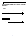
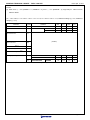
This document describes misstatements found in the RL78 hardware user’s manual Rev. 1.00 (R01UH0146EJ0100).
Corrections
User’s Manual
Applicable Page
Pages 5, 988
Page 93
Page 449
Pages 308, 860,
861, 864 to 867,
871, 872, 883, 884
Pages 493, 494,
526
Pages 631, 633,
658, 659, 661
Page 938
Page 983
Applicable Item
Industrial applications and extended-temperature
products released
Incorrect descriptions of recommended connection
of unused pins of P60 to P63 in table2-3 in pin
functions chapter revised
Incorrect descriptions of 7.4.2 Shifting to
HALT/STOP mode after starting operation, in
real-time clock chapter revised
Incorrect descriptions of reset processing
time/standby mode release time revised
Explanations of when using SNOOZE mode in A/D
converter chapter added
Caution of when using SNOOZE mode in serial
array unit chapter added
Explanations of data flash in flash memory chapter
added
Spec of on-chip oscillator characteristics in electrical
specifications chapter confirmed
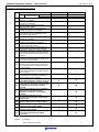
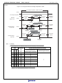
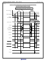
Contents
Products released
Incorrect descriptions
revised
Incorrect descriptions
revised
Incorrect descriptions
revised
Explanations added
Caution added
Explanations added
Spec confirmed
Incorrect: Bold with underline; Correct: Gray hatched
Document Improvement
The above corrections will be made for the next revision of the hardware user’s manual around March, 2012. Contact a
Renesas Electronics sales department details on the publishing schedule.
(c) 2012. Renesas Electronics Corporation. All rights reserved.
Page 1 of 70
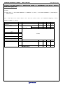
RENESAS TECHNICAL UPDATE TN-RL*-A001C/E
Date: April. 6, 2012
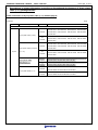
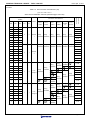
Corrections in the hardware user’s manual
Applicable Item
No.
1
2
3
4
5
6
7
8
9
10
11
12
13
14
15
16
17
18
19
20
21
22
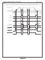
Japanese
English
Incorrect descriptions of 64-pin plastic
TQFP (7 x 7) deleted
Incorrect descriptions of count registers, in
real-time clock deleted
Explanations of interval timer control
register (ITMC) added
Explanations of timing chart when A/D
voltage comparator is used added
Incorrect descriptions of A/D conversion
time selection, there is stabilization wait
time (6/8) to (8/8) revised
Explanations when entering A/D converter
standby mode added
Incorrect descriptions of maskable interrupt
request acknowledgment operation
Incorrect descriptions of voltage detector
(LVD) timing chart revised
Incorrect descriptions of voltage detector
(LVD) interrupt and reset mode revised
Number (4) of Supply current characteristics
in Electrical specifications chapter (section
29.4.2) is the same for all RL78/G13 Group
products.
Explanations when using temperature
sensor and internal reference voltage (1.45
V) of A/D converter added
Explanations when using temperature
sensor and internal reference voltage (1.45
V) of A/D test function in Safety functions
chapter added
Conditions of A/D converter characteristics
in Electrical specifications chapter (section
29.7.1) added
Condition of Temperature sensor
characteristics in Electrical specifications
chapter (section 29.7.2) added
Industrial applications and
extended-temperature products released
Incorrect descriptions of recommended
connection of unused pins of P60 to P63
in table2-3 in pin functions chapter
revised
Incorrect descriptions of 7.4.2 Shifting to
HALT/STOP mode after starting
operation, in real-time clock chapter
revised
Incorrect descriptions of reset
processing time/standby mode release
time revised
Explanations of when using SNOOZE
mode in A/D converter chapter added
Caution of when using SNOOZE mode in
serial array unit chapter added
Explanations of data flash in flash
memory chapter added
Spec of on-chip oscillator characteristics
in electrical specifications chapter
confirmed
Document No.
Rev 1.00
R01UH0146JJ0100
R01UH0146EJ0100
After Rev 2.00Note
R01UH0146JJ0200
R01UH0146EJ0200
−
9
−
9
−
9
−
9
−
9
−
9
−
9
−
9
−
9
−
9
−
9
−
9
−
9
−
9
−
9
−
9
−
9
−
9
−
9
−
9
−
9
−
9
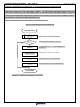
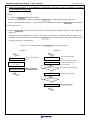
Note No.15 to 23 (bold text) are the corrections added in this notice.
Remarks 9: Corrected
−: Items should be corrected
Page 2 of 70
RENESAS TECHNICAL UPDATE TN-RL*-A001C/E
Date: April. 6, 2012
1. Descriptions of related information according to discontinued development of 64-pin plastic
TQFP (7 x 7) package deleted
Order information of 64-pin plastic TQFP (7 x 7) deleted (page 4)
Incorrect:
(2/3)
Pin count
Package
Data flash
Part Number
(Omitted)
R5F100LCAFA, R5F100LDAFA, R5F100LEAFA, R5F100LFAFA,
Mounted
R5F100LGAFA, R5F100LHAFA, R5F100LJAFA, R5F100LKAFA,
R5F100LLAFA
64-pin plastic LQFP (12x12)
Not
mounted
R5F101LCAFA, R5F101LDAFA, R5F101LEAFA, R5F101LFAFA,
R5F101LGAFA, R5F101LHAFA, R5F101LJAFA, R5F101LKAFA,
R5F101LLAFA
R5F100LCAFB, R5F100LDAFB, R5F100LEAFB, R5F100LFAFB,
Mounted
R5F100LLAFB
64-pin plastic LQFP (fine pitch)
64 pins
(10 × 10)
Not
mounted
64-pin plastic TQFP
(fine pitch) (7 × 7)
Mounted
Not
mounted
Mounted
64-pin plastic FBGA (4 × 4)
R5F100LGAFB, R5F100LHAFB, R5F100LJAFB, R5F100LKAFB,
Not
mounted
R5F101LCAFB, R5F101LDAFB, R5F101LEAFB, R5F101LFAFB,
R5F101LGAFB, R5F101LHAFB, R5F101LJAFB, R5F101LKAFB,
R5F101LLAFB
R5F100LCAFC, R5F100LDAFC, R5F100LEAFC, R5F100LFAFC,
R5F100LGAFC, R5F100LHAFC, R5F100LJAFC
R5F101LCAFC, R5F101LDAFC, R5F101LEAFC, R5F101LFAFC,
R5F101LGAFC, R5F101LHAFC, R5F101LJAFC
R5F100LCABG, R5F100LDABG, R5F100LEABG, R5F100LFABG,
R5F100LGABG, R5F100LHABG, R5F100LJABG
R5F101LCABG, R5F101LDABG, R5F101LEABG, R5F101LFABG,
R5F101LGABG, R5F101LHABG, R5F101LJABG
Page 3 of 70
RENESAS TECHNICAL UPDATE TN-RL*-A001C/E
Date: April. 6, 2012
Correct:
(2/3)
Pin count
Package
Data flash
Part Number
(Omitted)
R5F100LCAFA, R5F100LDAFA, R5F100LEAFA, R5F100LFAFA,
Mounted
R5F100LGAFA, R5F100LHAFA, R5F100LJAFA, R5F100LKAFA,
R5F100LLAFA
64-pin plastic LQFP (12x12)
Not
mounted
R5F101LCAFA, R5F101LDAFA, R5F101LEAFA, R5F101LFAFA,
R5F101LGAFA, R5F101LHAFA, R5F101LJAFA, R5F101LKAFA,
R5F101LLAFA
R5F100LCAFB, R5F100LDAFB, R5F100LEAFB, R5F100LFAFB,
Mounted
64 pins
R5F100LLAFB
64-pin plastic LQFP (fine pitch)
(10 × 10)
Not
mounted
Mounted
64-pin plastic FBGA (4 × 4)
R5F100LGAFB, R5F100LHAFB, R5F100LJAFB, R5F100LKAFB,
Not
mounted
R5F101LCAFB, R5F101LDAFB, R5F101LEAFB, R5F101LFAFB,
R5F101LGAFB, R5F101LHAFB, R5F101LJAFB, R5F101LKAFB,
R5F101LLAFB
R5F100LCABG, R5F100LDABG, R5F100LEABG, R5F100LFABG,
R5F100LGABG, R5F100LHABG, R5F100LJABG
R5F101LCABG, R5F101LDABG, R5F101LEABG, R5F101LFABG,
R5F101LGABG, R5F101LHABG, R5F101LJABG
Page 4 of 70
RENESAS TECHNICAL UPDATE TN-RL*-A001C/E
Date: April. 6, 2012
Pin configuration of 64-pin plastic TQFP (7 x 7) deleted (page 17)
Incorrect:
1.3.11 64-pin products
• 64-pin plastic LQFP (12 × 12)
• 64-pin plastic LQFP (fine pitch) (10 × 10)
• 64-pin plastic TQFP (fine pitch) (7 × 7)
(Omitted)
Correct:
1.3.11 64-pin products
• 64-pin plastic LQFP (12 × 12)
• 64-pin plastic LQFP (fine pitch) (10 × 10)
(Omitted)
Package drawings of 64-pin plastic TQFP (7 x 7) deleted (page 1055)
Incorrect:
R5F100LCAFC, R5F100LDAFC, R5F100LEAFC, R5F100LFAFC, R5F100LGAFC, R5F100LHAFC, R5F100LJAFC
R5F101LCAFC, R5F101LDAFC, R5F101LEAFC, R5F101LFAFC, R5F101LGAFC, R5F101LHAFC, R5F101LJAFC
64-PIN PLASTIC TQFP (7x7)
Under development
Correct: Applicable page deleted
Page 5 of 70
RENESAS TECHNICAL UPDATE TN-RL*-A001C/E
Date: April. 6, 2012
2. Incorrect descriptions of count registers in real-time clock deleted
Incorrect description of second count register (SEC) in real-time clock deleted (page 439)
Incorrect:
(5) Second count register (SEC)
The SEC register is an 8-bit register that takes a value of 0 to 59 (decimal) and indicates the count value of seconds.
It counts up when the sub-count register overflows.
When data is written to this register, it is written to a buffer and then to the counter up to 2 clocks (fRTC) later. Set a decimal
value of 00 to 59 to this register in BCD code. If a value outside the range is set, the register value returns to the
normal value after 1 period.
The SEC register can be set by an 8-bit memory manipulation instruction.
Reset signal generation clears this register to 00H.
Correct:
(5) Second count register (SEC)
The SEC register is an 8-bit register that takes a value of 0 to 59 (decimal) and indicates the count value of seconds.
It counts up when the sub-count register overflows. When data is written to this register, it is written to a buffer and then to
the counter up to 2 clocks (fRTC) later. Set a decimal value of 00 to 59 to this register in BCD code.
The SEC register can be set by an 8-bit memory manipulation instruction.
Reset signal generation clears this register to 00H.
Page 6 of 70
RENESAS TECHNICAL UPDATE TN-RL*-A001C/E
Date: April. 6, 2012
Incorrect description of minute count register (MIN) in real-time clock deleted (page 439)
Incorrect:
(6) Minute count register (MIN)
The MIN register is an 8-bit register that takes a value of 0 to 59 (decimal) and indicates the count value of minutes.
It counts up when the second counter overflows.
When data is written to this register, it is written to a buffer and then to the counter up to 2 clocks (fRTC) later. Even if the
second count register overflows while this register is being written, this register ignores the overflow and is set to the value
written. Set a decimal value of 00 to 59 to this register in BCD code. If a value outside the range is set, the register value
returns to the normal value after 1 period.
The MIN register can be set by an 8-bit memory manipulation instruction.
Reset signal generation clears this register to 00H.
Correct:
(6) Minute count register (MIN)
The MIN register is an 8-bit register that takes a value of 0 to 59 (decimal) and indicates the count value of minutes.
It counts up when the second counter overflows.
When data is written to this register, it is written to a buffer and then to the counter up to 2 clocks (fRTC) later. Even if the
second count register overflows while this register is being written, this register ignores the overflow and is set to the value
written. Set a decimal value of 00 to 59 to this register in BCD code.
The MIN register can be set by an 8-bit memory manipulation instruction.
Reset signal generation clears this register to 00H.
Page 7 of 70
RENESAS TECHNICAL UPDATE TN-RL*-A001C/E
Date: April. 6, 2012
Incorrect description of hour count register (HOUR) in real-time clock deleted (page 440)
Incorrect:
(7) Hour count register (HOUR)
The HOUR register is an 8-bit register that takes a value of 00 to 23 or 01 to 12 and 21 to 32 (decimal) and indicates the
count value of hours.
It counts up when the minute counter overflows.
When data is written to this register, it is written to a buffer and then to the counter up to 2 clocks (fRTC) later. Even if the
minute count register overflows while this register is being written, this register ignores the overflow and is set to the value
written. Specify a decimal value of 00 to 23, 01 to 12, or 21 to 32 by using BCD code according to the time system specified
using bit 3 (AMPM) of real-time clock control register 0 (RTCC0). If the AMPM bit value is changed, the values of the HOUR
register change according to the specified time system. If a value outside the range is set, the register value returns to
the normal value after 1 period.
The HOUR register can be set by an 8-bit memory manipulation instruction.
Reset signal generation clears this register to 12H.
However, the value of this register is 00H if the AMPM bit (bit 3 of the RTCC0 register) is set to 1 after reset.
Correct:
(7) Hour count register (HOUR)
The HOUR register is an 8-bit register that takes a value of 00 to 23 or 01 to 12 and 21 to 32 (decimal) and indicates the
count value of hours.
It counts up when the minute counter overflows.
When data is written to this register, it is written to a buffer and then to the counter up to 2 clocks (fRTC) later. Even if the
minute count register overflows while this register is being written, this register ignores the overflow and is set to the value
written. Specify a decimal value of 00 to 23, 01 to 12, or 21 to 32 by using BCD code according to the time system specified
using bit 3 (AMPM) of real-time clock control register 0 (RTCC0). If the AMPM bit value is changed, the values of the HOUR
register change according to the specified time system.
The HOUR register can be set by an 8-bit memory manipulation instruction.
Reset signal generation clears this register to 12H.
However, the value of this register is 00H if the AMPM bit (bit 3 of the RTCC0 register) is set to 1 after reset.
Page 8 of 70
RENESAS TECHNICAL UPDATE TN-RL*-A001C/E
Date: April. 6, 2012
Incorrect description of day count register (DAY) in real-time clock deleted (page 442)
Incorrect:
(8) Day count register (DAY)
The DAY register is an 8-bit register that takes a value of 1 to 31 (decimal) and indicates the count value of days.
It counts up when the hour counter overflows.
This counter counts as follows.
(Omitted)
When data is written to this register, it is written to a buffer and then to the counter up to 2 clocks (fRTC) later. Even if the
hour count register overflows while this register is being written, this register ignores the overflow and is set to the value
written. Set a decimal value of 01 to 31 to this register in BCD code. If a value outside the range is set, the register value
returns to the normal value after 1 period.
The DAY register can be set by an 8-bit memory manipulation instruction.
Reset signal generation clears this register to 01H.
Correct:
(8) Day count register (DAY)
The DAY register is an 8-bit register that takes a value of 1 to 31 (decimal) and indicates the count value of days.
It counts up when the hour counter overflows.
This counter counts as follows.
(Omitted)
When data is written to this register, it is written to a buffer and then to the counter up to 2 clocks (fRTC) later. Even if the
hour count register overflows while this register is being written, this register ignores the overflow and is set to the value
written. Set a decimal value of 01 to 31 to this register in BCD code.
The DAY register can be set by an 8-bit memory manipulation instruction.
Reset signal generation clears this register to 01H.
Page 9 of 70
RENESAS TECHNICAL UPDATE TN-RL*-A001C/E
Date: April. 6, 2012
Incorrect description of week count register (WEEK) in real-time clock deleted (page 443)
Incorrect:
(9) Week count register (WEEK)
The WEEK register is an 8-bit register that takes a value of 0 to 6 (decimal) and indicates the count value of weekdays.
It counts up in synchronization with the day counter.
When data is written to this register, it is written to a buffer and then to the counter up to 2 clocks (fRTC) later. Set a decimal
value of 00 to 06 to this register in BCD code. If a value outside the range is set, the register value returns to the
normal value after 1 period.
The WEEK register can be set by an 8-bit memory manipulation instruction.
Reset signal generation clears this register to 00H.
Correct:
(9) Week count register (WEEK)
The WEEK register is an 8-bit register that takes a value of 0 to 6 (decimal) and indicates the count value of weekdays.
It counts up in synchronization with the day counter.
When data is written to this register, it is written to a buffer and then to the counter up to 2 clocks (fRTC) later. Set a decimal
value of 00 to 06 to this register in BCD code.
The WEEK register can be set by an 8-bit memory manipulation instruction.
Reset signal generation clears this register to 00H.
Page 10 of 70
RENESAS TECHNICAL UPDATE TN-RL*-A001C/E
Date: April. 6, 2012
Incorrect description of month count register (MONTH) in real-time clock deleted (page 444)
Incorrect:
(10) Month count register (MONTH)
The MONTH register is an 8-bit register that takes a value of 1 to 12 (decimal) and indicates the count value of months.
It counts up when the day counter overflows.
When data is written to this register, it is written to a buffer and then to the counter up to 2 clocks (fRTC) later. Even if the
day count register overflows while this register is being written, this register ignores the overflow and is set to the value
written. Set a decimal value of 01 to 12 to this register in BCD code. If a value outside the range is set, the register
value returns to the normal value after 1 period.
The MONTH register can be set by an 8-bit memory manipulation instruction.
Reset signal generation clears this register to 01H.
Correct:
(10) Month count register (MONTH)
The MONTH register is an 8-bit register that takes a value of 1 to 12 (decimal) and indicates the count value of months.
It counts up when the day counter overflows.
When data is written to this register, it is written to a buffer and then to the counter up to 2 clocks (fRTC) later. Even if the
day count register overflows while this register is being written, this register ignores the overflow and is set to the value
written. Set a decimal value of 01 to 12 to this register in BCD code.
The MONTH register can be set by an 8-bit memory manipulation instruction.
Reset signal generation clears this register to 01H.
Page 11 of 70
RENESAS TECHNICAL UPDATE TN-RL*-A001C/E
Date: April. 6, 2012
Incorrect description of year count register (YEAR) in real-time clock deleted (page 444)
Incorrect:
(11) Year count register (YEAR)
The YEAR register is an 8-bit register that takes a value of 0 to 99 (decimal) and indicates the count value of years.
It counts up when the month count register (MONTH) overflows.
Values 00, 04, 08, …, 92, and 96 indicate a leap year.
When data is written to this register, it is written to a buffer and then to the counter up to 2 clocks (fRTC) later. Even if the
MONTH register overflows while this register is being written, this register ignores the overflow and is set to the value
written. Set a decimal value of 00 to 99 to this register in BCD code. If a value outside the range is set, the register
value returns to the normal value after 1 period.
The YEAR register can be set by an 8-bit memory manipulation instruction.
Reset signal generation clears this register to 00H.
Correct:
(11) Year count register (YEAR)
The YEAR register is an 8-bit register that takes a value of 0 to 99 (decimal) and indicates the count value of years.
It counts up when the month count register (MONTH) overflows.
Values 00, 04, 08, …, 92, and 96 indicate a leap year.
When data is written to this register, it is written to a buffer and then to the counter up to 2 clocks (fRTC) later. Even if the
MONTH register overflows while this register is being written, this register ignores the overflow and is set to the value
written. Set a decimal value of 00 to 99 to this register in BCD code.
The YEAR register can be set by an 8-bit memory manipulation instruction.
Reset signal generation clears this register to 00H.
Page 12 of 70
RENESAS TECHNICAL UPDATE TN-RL*-A001C/E
Date: April. 6, 2012
3. Caution of interval timer control register (ITMC) in 12-bit interval timer added (page 460)
Incorrect:
(3) Interval timer control register (ITMC)
(Omitted)
Cautions 1. Before changing the RINTE bit from 1 to 0, use the interrupt mask flag register to disable the INTIT interrupt
servicing. When the operation starts (from 0 to 1) again, clear the ITIF flag, and then enable the interrupt servicing.
2. The value read from the RINTE bit is applied one count clock cycle after setting the RINTE bit.
3. Only change the setting of the ITCMP11 to ITCMP0 bits when RINTE = 0. However, it is possible to change the
settings of the ITCMP11 to ITCMP0 bits at the same time as when changing RINTE from 0 to 1 or 1 to 0.
Correct:
(3) Interval timer control register (ITMC)
(Omitted)
Cautions 1. Before changing the RINTE bit from 1 to 0, use the interrupt mask flag register to disable the INTIT interrupt
servicing. When the operation starts (from 0 to 1) again, clear the ITIF flag, and then enable the interrupt
servicing.
2. The value read from the RINTE bit is applied one count clock cycle after setting the RINTE bit.
3. When setting the RINTE bit after returned from standby mode and entering standby mode again, confirm that the
written value of the RINTE bit is reflected, or wait that more than one clock of the count clock has elapsed after
returned from standby mode. Then enter standby mode.
4. Only change the setting of the ITCMP11 to ITCMP0 bits when RINTE = 0. However, it is possible to change the
settings of the ITCMP11 to ITCMP0 bits at the same time as when changing RINTE from 0 to 1 or 1 to 0.
Page 13 of 70
RENESAS TECHNICAL UPDATE TN-RL*-A001C/E
Date: April. 6, 2012
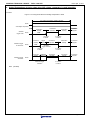
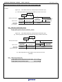
4. Added Explanations of timing chart when A/D voltage comparator is used (page 483)
Incorrect:
Figure 11-4. Timing Chart When A/D Voltage Comparator Is Used
A/D voltage comparator: enables operation
ADCE
A/D voltage comparator
Conversion
operation
Conversion
standby
Software
trigger mode
ADCS
Conversion
standby
ADCS
Trigger
standby
0 is written
to ADCS.
Conversion
operation
Conversion
standby
Conversion
stopped
Note
Hardware
trigger detection
1 is written
to ADCS.
Conversion
standby
Hardware trigger
wait mode
Conversion
stopped
Note
1 is written
to ADCS.
Hardware trigger
no-wait mode
Conversion
standby
Stabilization
wait time
0 is written
to ADCS.
Conversion
operation
Conversion
standby
Conversion
stopped
ADCS
Hardware trigger
detection
0 is written
to ADCS.
Note (Omitted)
Page 14 of 70
RENESAS TECHNICAL UPDATE TN-RL*-A001C/E
Date: April. 6, 2012
Correct:
Figure 11-4. Timing Chart When A/D Voltage Comparator Is Used
A/D voltage comparator: enables operation
ADCE
A/D voltage comparator
Conversion
standby
Software
trigger mode
ADCS
Conversion
standby
ADCS
Trigger
standby
0 is written
to ADCS.
Conversion start Note 2
Conversion
Conversion
operation
standby
Conversion
stopped
Note 1
Hardware
trigger detection
0 is written
1 is written
Conversion startNote 2 to ADCS.
to ADCS.
A/D power stabilization
wait time
Conversion
operation
Conversion
standby
Hardware trigger
wait mode
Conversion
stopped
Note 1
1 is written
to ADCS.
Hardware trigger
no-wait mode
Conversion startNote 2
Conversion
Conversion
operation
standby
Conversion
stopped
ADCS
Hardware trigger
detection
Note
Conversion
standby
0 is written
to ADCS.
1. (Omitted)
2. The following time is the maximum amount of time necessary to start conversion.
ADM0
Conversion
Conversion Start Time (Number of fCLK Clocks)
FR2 FR1 FR0
Clock
Software trigger mode/
(fAD)
Hardware trigger no wait mode
0
0
0
fCLK/64
63
0
0
1
fCLK/32
31
0
1
0
fCLK/16
15
0
1
1
fCLK/8
7
1
0
0
fCLK/6
5
1
0
1
fCLK/5
4
1
1
0
fCLK/4
3
1
1
1
fCLK/2
1
Hardware trigger wait mode
1
Remark fCLK: CPU/peripheral hardware clock frequency
Page 15 of 70
RENESAS TECHNICAL UPDATE TN-RL*-A001C/E
Date: April. 6, 2012
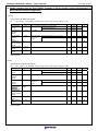
5. Incorrect descriptions of Table 11-3 A/D Conversion Time Selection (6/8) to (8/8) when there
is stabilization wait time (pages 489 to 491)
Incorrect:
Table 11-3. A/D Conversion Time Selection (6/8)
(6) 2.7 V ≤ VDD < 3.6 V
Conversion Time Selection
(ADM0)
FR2
FR1
FR0
0
0
0
0
0
1
0
1
0
0
1
1
1
0
0
1
0
1
1
1
0
1
1
1
0
0
0
0
0
1
0
1
0
0
1
1
1
0
0
1
0
1
1
1
0
1
1
1
0
0
0
0
0
1
0
1
0
0
1
1
1
0
0
1
0
1
1
1
0
1
1
1
0
0
0
0
0
1
0
1
0
0
1
1
1
0
0
1
0
1
1
1
0
1
1
1
Mode
LV1
LV0
fCLK =
fCLK =
fCLK =
fCLK =
1 MHz
2 MHz
4 MHz
8 MHz
Normal
0
0
1
Setting
prohibited
prohibited 54 μs
54 μs
54 μs
27 μs
13.5 μs
40.5 μs
20.25 μs
10.125 μs 5.0625 μs
33.75 μs
16.875 μs 8.4375 μs
27 μs
13.5 μs
13.5 μs
0
1
Normal
prohibited
50 μs
50 μs
25 μs
Low1
0
Voltage
Setting
prohibited
1
1
Voltage
prohibited
12.5 μs
fCLK/16
50 μs
25 μs
12.5 μs
6.25 μs
fCLK/8
37.5 μs
18.75 μs
9.375 μs
4.6875 μs
fCLK/6
31.25 μs
15.625 μs 7.8125 μs
25 μs
12.5 μs
12.5 μs
prohibited
6.25 μs
prohibited
6.25 μs
Setting
Setting
prohibited
prohibited
Setting
54 μs
prohibited
prohibited
54 μs
27 μs
prohibited
54 μs
27 μs
54 μs
27 μs
27 μs
Setting
Setting
27 μs
Setting
prohibited
Setting
prohibited
50 μs
25 μs
25 μs
Setting
prohibited
fCLK/64
fCLK/32
fCLK/16
Setting
prohibited
fCLK/5
fCLK/4
fCLK/2
Setting
Setting
50 μs
prohibited
prohibited 50 μs
25 μs
25 μs
Setting
prohibited
fCLK/64
fCLK/32
fCLK/16
25 μs
fCLK/8
37.5 μs
31.25 μs
fCLK/2
fCLK/6
50 μs
50 μs
fCLK/4
fCLK/8
prohibited
Setting
2
50 μs
fCLK/5
40.5 μs
prohibited
fCLK/2
25 μs
prohibited
Setting
fCLK/4
50 μs
Setting
Low-
prohibited
fCLK/32
Setting
33.75 μs
54 μs
Setting
25 μs
prohibited 54 μs
1
fCLK/6
fCLK/5
prohibited
Setting
fCLK/8
50 μs
Setting
Setting
Setting
fCLK/32
fCLK/16
fCLK/64
Setting
2
6.75 μs
6.75 μs
6.75 μs
fCLK/64
50 μs
prohibited
prohibited
32 MHz
54 μs
27 μs
Setting
Setting
16 MHz
Setting
fCLK =
prohibited
prohibited
54 μs
27 μs
prohibited
54 μs
27 μs
13.5 μs
Setting
Setting
Setting
fCLK =
Clock (fAD)
A/D Converter Mode Register 0
Conversion
When there is stabilization wait time (hardware trigger wait mode)
Setting
prohibited
Setting
prohibited
fCLK/6
fCLK/5
fCLK/4
fCLK/2
Page 16 of 70
RENESAS TECHNICAL UPDATE TN-RL*-A001C/E
Date: April. 6, 2012
Incorrect:
Table 11-3. A/D Conversion Time Selection (7/8)
(7) 1.8 V ≤ VDD < 2.7 V
Conversion Time Selection
(ADM0)
Mode
FR2
FR1
FR0
LV1
LV0
fCLK =
fCLK =
fCLK =
fCLK =
1 MHz
2 MHz
4 MHz
8 MHz
fCLK =
16 MHz
(Note)
fCLK =
32 MHz
Clock (fAD)
A/D Converter Mode Register 0
Conversion
When there is stabilization wait time (hardware trigger wait mode)
0
0
0
fCLK/64
0
0
1
fCLK/32
0
1
0
fCLK/16
0
1
1
1
0
0
1
0
1
fCLK/5
1
1
0
fCLK/4
1
1
1
fCLK/2
0
0
0
Setting
prohibited prohibited prohibited prohibited prohibited prohibited
0
0
Normal Setting
1
Setting
Setting
Setting
Setting
Setting
prohibited prohibited prohibited prohibited prohibited prohibited
Setting
Setting
Setting
Setting
Setting
fCLK/8
fCLK/6
fCLK/64
0
0
1
0
1
0
0
1
1
1
0
0
1
0
1
fCLK/5
1
1
0
fCLK/4
1
1
1
fCLK/2
0
0
0
0
0
1
0
0
1
1
1
0
0
1
0
1
1
1
fCLK/16
0
1
Normal
fCLK/8
2
fCLK/6
Setting
1
0
Setting
1
0
Low-
prohibited
1
1
0
0
0
Setting
prohibited
prohibited
0
0
1
33.75 μs
54 μs
54 μs
27 μs
1
0
1
1
1
0
0
1
0
1
1
1
0
1
1
1
Setting
1
1
Low-
Setting
prohibited
54 μs
27 μs
prohibited
Setting
prohibited
50 μs
25 μs
fCLK/32
27 μs
fCLK/16
fCLK/8
Setting
prohibited
Setting
prohibited
50 μs
25 μs
Setting
prohibited
fCLK/6
fCLK/5
fCLK/4
fCLK/2
Setting
prohibited
50 μs
31.25 μs
50 μs
27 μs
27 μs
Setting
prohibited
50 μs
50 μs
fCLK/64
25 μs
fCLK/32
25 μs
fCLK/16
25 μs
fCLK/8
37.5 μs
Voltage 2
fCLK/64
prohibited
Setting
prohibited
54 μs
Setting
prohibited
0
prohibited
54 μs
54 μs
Setting
0
Setting
40.5 μs
Voltage 1
0
1
fCLK/32
Setting
prohibited
Setting
prohibited
Setting
prohibited
fCLK/6
fCLK/5
fCLK/4
fCLK/2
Note (Omitted)
Page 17 of 70
RENESAS TECHNICAL UPDATE TN-RL*-A001C/E
Date: April. 6, 2012
Incorrect:
Table 11-3. A/D Conversion Time Selection (8/8)
(8) 1.6 V ≤ VDD < 1.8 V
A/D Converter Mode Register 0
Conversion Time Selection
(ADM0)
Mode
FR2
FR1
FR0
LV1
LV0
fCLK =
fCLK =
fCLK =
fCLK =
1 MHz
2 MHz
4 MHz
8 MHz
fCLK =
16 MHz
(Note 2)
fCLK =
32 MHz
Conversion
Clock (fAD)
When there is stabilization wait time (hardware trigger wait mode)
0
0
0
fCLK/64
0
0
1
fCLK/32
0
1
0
fCLK/16
0
1
1
1
0
0
1
0
1
fCLK/5
1
1
0
fCLK/4
1
1
1
fCLK/2
0
0
0
fCLK/64
0
0
1
fCLK/32
0
1
0
fCLK/16
0
1
1
1
0
0
1
0
1
fCLK/5
1
1
0
fCLK/4
1
1
1
fCLK/2
0
0
0
0
0
0
1
Normal
1
Normal
2
Setting
prohibited prohibited
Setting
Setting
0
1
Setting
0
1
0
prohibited
0
1
1
1
0
0
1
0
1
135 μs
0
108 μs
1
1
1
1
0
0
0
1
0
Voltage 1
81 μs
Setting
0
1
0
prohibited
0
1
1
1
0
0
1
0
1
1
1
Setting
Setting
prohibited prohibited prohibited prohibited
Setting
Setting
Setting
Setting
prohibited prohibited prohibited prohibited
Setting
prohibited
Setting
Setting
Setting
prohibited
108 μs
prohibited
1
1
prohibited
108 μs
100 μs
Setting
prohibited
prohibited
fCLK/6
fCLK/16
Setting
prohibited
Setting
Setting
fCLK/8
prohibited
fCLK/6
prohibited
fCLK/5
fCLK/4
Setting
prohibited
Setting
prohibited
100 μs
fCLK/64
100 μs
fCLK/32
100 μs
Setting
fCLK/8
fCLK/2
Voltage 2
125 μs
fCLK/6
fCLK/32
fCLK/16
100 μs
Low-
fCLK/8
fCLK/64
prohibited
Setting
Setting
1
Setting
prohibited
1
0
Setting
108 μs
Low-
0
1
prohibited
108 μs
0
1
Setting
prohibited prohibited
0
1
Setting
Setting
prohibited
Setting
prohibited
Setting
prohibited
Setting
fCLK/8
prohibited
fCLK/6
fCLK/5
fCLK/4
fCLK/2
Note (Omitted)
Page 18 of 70
RENESAS TECHNICAL UPDATE TN-RL*-A001C/E
Date: April. 6, 2012
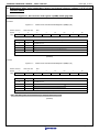
Correct:
Table 11-3. A/D Conversion Time Selection (6/8)
(6) 2.7 V ≤ VDD < 3.6 V
Conversion Time Selection
(ADM0)
FR2
FR1
FR0
0
0
0
0
0
1
0
1
0
0
1
1
1
0
0
1
0
1
1
1
0
1
1
1
0
0
0
0
0
1
0
1
0
0
1
1
1
0
0
1
0
1
1
1
0
1
1
1
0
0
0
Mode
LV1
LV0
fCLK =
fCLK =
fCLK =
fCLK =
1 MHz
2 MHz
4 MHz
8 MHz
Normal
0
0
1
Setting
prohibited
prohibited 54 μs
54 μs
54 μs
27 μs
13.5 μs
40.5 μs
20.25 μs
10.125 μs 5.0625 μs
33.75 μs
16.875 μs 8.4375 μs
27 μs
13.5 μs
13.5 μs
0
1
Normal
prohibited
50 μs
50 μs
25 μs
0
1
0
1
0
0
1
1
1
0
0
1
0
1
1
1
0
1
1
1
0
0
0
0
0
1
0
1
0
0
1
1
1
0
0
1
0
1
1
1
0
1
1
1
1
0
Voltage
Setting
prohibited
12.5 μs
fCLK/16
50 μs
25 μs
12.5 μs
6.25 μs
fCLK/8
37.5 μs
18.75 μs
9.375 μs
4.6875 μs
fCLK/6
31.25 μs
15.625 μs 7.8125 μs
25 μs
12.5 μs
12.5 μs
prohibited
6.25 μs
Setting
prohibited
42 μs
42 μs
42 μs
21 μs
21 μs
Setting
prohibited
6.25 μs
Setting
fCLK/5
Setting
prohibited
prohibited
Setting
prohibited
42 μs
Low1
1
Voltage
prohibited
prohibited
21 μs
fCLK/32
fCLK/16
21 μs
fCLK/8
21 μs
fCLK/6
Setting
prohibited
Setting
prohibited
Setting
prohibited
Setting
fCLK/4
Setting
19 μs
23.75μs
38 μs
38 μs
19 μs
19 μs
Setting
prohibited
Setting
prohibited
fCLK/64
fCLK/32
fCLK/16
19 μs
fCLK/8
28.5 μs
2
fCLK/5
fCLK/2
38 μs
38 μs
fCLK/2
fCLK/64
38 μs
prohibited
prohibited 38 μs
19 μs
prohibited
Setting
fCLK/4
42 μs
prohibited
Setting
Setting
fCLK/2
25 μs
26.25 μs
42 μs
fCLK/4
50 μs
Setting
31.5 μs
1
prohibited
fCLK/32
Setting
prohibited
Setting
25 μs
prohibited
Low-
fCLK/6
fCLK/5
prohibited
Setting
fCLK/8
50 μs
Setting
0
Setting
fCLK/32
fCLK/16
fCLK/64
Setting
2
6.75 μs
6.75 μs
6.75 μs
fCLK/64
50 μs
prohibited
prohibited
32 MHz
54 μs
27 μs
Setting
Setting
16 MHz
Setting
fCLK =
prohibited
prohibited
54 μs
27 μs
prohibited
54 μs
27 μs
13.5 μs
Setting
Setting
Setting
fCLK =
Clock (fAD)
A/D Converter Mode Register 0
Conversion
When there is stabilization wait time (hardware trigger wait mode)
Setting
prohibited
Setting
prohibited
fCLK/6
fCLK/5
fCLK/4
fCLK/2
Page 19 of 70
RENESAS TECHNICAL UPDATE TN-RL*-A001C/E
Date: April. 6, 2012
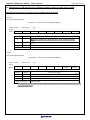
Correct:
Table 11-3. A/D Conversion Time Selection (7/8)
(7) 1.8 V ≤ VDD < 2.7 V
FR2
FR1
FR0
LV1
LV0
x
x
x
0
0
x
x
x
0
1
0
0
0
0
0
1
0
1
0
0
1
1
1
0
0
1
0
1
1
1
0
1
1
1
0
0
0
Conversion Time Selection
Mode
fCLK =
1 MHz
fCLK =
2 MHz
Normal
1
Normal
2
fCLK =
4 MHz
Setting
1
0
Low-
prohibited
prohibited
0
0
1
42 μs
21 μs
1
prohibited
0
1
1
1
0
0
1
1
1
0
1
1
1
1
Low-
21 μs
prohibited
Setting
prohibited
42 μs
prohibited
prohibited
38 μs
38 μs
19 μs
21 μs
fCLK/32
21 μs
fCLK/16
fCLK/8
Setting
prohibited
Setting
prohibited
fCLK/6
Setting
prohibited
Setting
prohibited
38 μs
38 μs
19 μs
Setting
prohibited
fCLK/5
fCLK/4
fCLK/2
prohibited
28.75 μs
0
fCLK/64
21 μs
Setting
prohibited
38 μs
38 μs
fCLK/64
19 μs
fCLK/32
19 μs
fCLK/16
19 μs
fCLK/8
28.5 μs
Voltage 2
42 μs
Setting
Setting
1
1
Setting
42 μs
42 μs
prohibited
Setting
32 MHz
−
26.25 μs
42 μs
fCLK =
Setting prohibited
31.5 μs
Voltage 1
0
16 MHz
Note
−
Setting
0
8 MHz
fCLK =
Setting prohibited
Setting
Setting
fCLK =
on
A/D Converter Mode Register 0 (ADM0)
Clock
When there is stabilization wait time (hardware trigger wait mode)
Setting
prohibited
Setting
prohibited
fCLK/6
Setting
prohibited
fCLK/5
fCLK/4
fCLK/2
Note (Omitted)
Page 20 of 70
RENESAS TECHNICAL UPDATE TN-RL*-A001C/E
Date: April. 6, 2012
Correct:
Table 11-3. A/D Conversion Time Selection (8/8)
(8) 1.6 V ≤ VDD < 1.8 V
A/D Converter Mode Register 0
Conversion Time Selection
(ADM0)
Mode
FR2
FR1
FR0
LV1
LV0
Normal
fCLK =
fCLK =
fCLK =
fCLK =
1 MHz
2 MHz
4 MHz
8 MHz
−
x
−
x
Setting
x
x
x
0
0
x
x
x
0
1
0
0
0
0
0
1
Setting
0
1
0
prohibited
0
1
1
1
0
0
1
0
1
105 μs
1
1
0
84 μs
1
1
1
0
0
0
0
0
1
Setting
0
1
0
prohibited
0
1
1
1
0
0
1
0
1
95 μs
1
1
0
76 μs
1
1
1
1
Normal
2
prohibited
Setting
prohibited
Setting
1
0
prohibited
Setting
prohibited
fCLK =
16 MHz
Note 2
32 MHz
x
x
0
0
x
x
0
1
Setting
prohibited
84 μs
fCLK/32
84 μs
63 μs
Voltage 1
Setting
fCLK/64
84 μs
fCLK/16
84 μs
Low-
fCLK =
Setting
Setting
prohibited
Setting
prohibited
Setting
Setting
fCLK/8
prohibited
fCLK/6
prohibited
fCLK/5
fCLK/4
prohibited
fCLK/2
prohibited
Setting
1
1
prohibited
Setting
prohibited
Setting
prohibited
76 μs
fCLK/32
76 μs
Voltage 2
Setting
prohibited
fCLK/64
76 μs
fCLK/16
76 μs
Low-
Setting
prohibited
Conversion
Clock (fAD)
When there is stabilization wait time (hardware trigger wait mode)
Setting
prohibited
Setting
prohibited
Setting
prohibited
Setting
fCLK/8
prohibited
fCLK/6
fCLK/5
fCLK/4
fCLK/2
Note (Omitted)
Page 21 of 70
RENESAS TECHNICAL UPDATE TN-RL*-A001C/E
Date: April. 6, 2012
6. Note when entering A/D converter standby mode added
Note on A/D converter mode register 2 (ADM2) added (page 493)
Incorrect:
(4) A/D converter mode register 2 (ADM2)
(Omitted)
Caution Only rewrite the value of the ADM2 register while conversion operation is stopped (which is indicated by the ADCS bit
of A/D converter mode register 0 (ADM0) being 0).
Correct:
(4) A/D converter mode register 2 (ADM2)
(Omitted)
Cautions 1. Only rewrite the value of the ADM2 register while conversion operation is stopped (which is indicated by the ADCS
bit of A/D converter mode register 0 (ADM0) being 0).
2. When entering STOP mode or HALT mode while the CPU is operating on the subsystem clock, do not set
ADREFP1 to 1. When selecting internal reference voltage (ADREFP1, ADREFP0 = 1, 0), the current value of A/D
converter reference voltage current (IADREF) shown in 29.4.2 Supply current characteristics is added.
Page 22 of 70
RENESAS TECHNICAL UPDATE TN-RL*-A001C/E
Date: April. 6, 2012
Note on analog input channel specification register (ADS) added (page 497)
Incorrect:
Figure 11-11. Format of Analog Input Channel Specification Register (ADS) (2/2)
Address: FFF31H
After reset: 00H R/W
Symbol
7
6
5
4
3
2
1
0
ADS
ADISS
0
0
ADS4
ADS3
ADS2
ADS1
ADS0
(Omitted)
Cautions 1. Be sure to clear bits 5 and 6 to 0.
(Omitted)
6. If using AVREFP as the + side reference voltage source of the A/D converter, do not select ANI0 as an A/D
conversion channel.
7. If using AVREFM as the − side reference voltage source of the A/D converter, do not select ANI1 as an A/D
conversion channel.
8. If ADISS is set to 1, the internal reference voltage (1.45 V) cannot be used for the + side reference voltage source.
Correct:
Figure 11-11. Format of Analog Input Channel Specification Register (ADS) (2/2)
Address: FFF31H
After reset: 00H R/W
Symbol
7
6
5
4
3
2
1
0
ADS
ADISS
0
0
ADS4
ADS3
ADS2
ADS1
ADS0
(Omitted)
Cautions 1. Be sure to clear bits 5 and 6 to 0.
(Omitted)
6. If using AVREFP as the + side reference voltage source of the A/D converter, do not select ANI0 as an A/D
conversion channel.
7. If using AVREFM as the − side reference voltage source of the A/D converter, do not select ANI1 as an A/D
conversion channel.
8. If ADISS is set to 1, the internal reference voltage (1.45 V) cannot be used for the + side reference voltage source.
9. When entering STOP mode or HALT mode while the CPU is operating on the subsystem clock, do not set ADISS to
1. When setting ADISS to 1, the current value of the A/D converter reference voltage current (IADREF) shown in
29.4.2 Supply current characteristics is added.
Page 23 of 70
RENESAS TECHNICAL UPDATE TN-RL*-A001C/E
Date: April. 6, 2012
7. Incorrect descriptions of maskable interrupt request acknowledgement operation revised
Revised incorrect description of time from generation of maskable interrupt until servicing in Table 16-4.
(page 842)
Incorrect:
16.4.1 Maskable interrupt request acknowledgment
(Omitted)
Table 16.4 Time from Generation of Maskable Interrupt Until Servicing
Minimum Time
Servicing time
9 clocks
Maximum TimeNote
14 clocks
Note If an interrupt request is generated just before the RET instruction, the wait time becomes longer.
Remark 1 clock: 1/fCLK (fCLK: CPU clock)
Correct:
16.4.1 Maskable interrupt request acknowledgment
(Omitted)
Table 16.4 Time from Generation of Maskable Interrupt Until Servicing
Minimum Time
Servicing time
9 clocks
Maximum TimeNote
16 clocks
Note Maximum time does not apply when an instruction from the internal RAM area is executed.
Remark 1 clock: 1/fCLK (fCLK: CPU clock)
Page 24 of 70
RENESAS TECHNICAL UPDATE TN-RL*-A001C/E
Date: April. 6, 2012
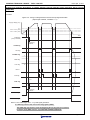
Figure 16-9. Incorrect description of interrupt request acknowledgment timing (maximum time) revised
(page 844)
Incorrect:
Figure 16-9. Interrupt Request Acknowledgment Timing (Maximum Time)
CPU processing
Instruction
6 clocks
6 clocks
RET instruction
PSW and PC saved,
jump to interrupt
servicing
Interrupt servicing
program
xxIF
14 clocks
Remark 1 clock: 1/fCLK (fCLK: CPU clock)
Correct:
Figure 16-9. Interrupt Request Acknowledgment Timing (Maximum Time)
8 clocks
CPU processing
Instruction
Instruction immediately
before interrupt
6 clocks
PSW and PC saved,
jump to interrupt
servicing
Interrupt servicing
program
××IF
16 clocks
Remark 1 clock: 1/fCLK (fCLK: CPU clock)
Page 25 of 70
RENESAS TECHNICAL UPDATE TN-RL*-A001C/E
Date: April. 6, 2012
8. Incorrect descriptions of voltage detector (LVD) timing chart revised
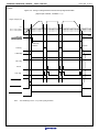
Figure 21-4. Incorrect descriptions of timing of voltage detector internal reset signal generation revised
(page 894)
Incorrect:
Figure 21-4. Timing of Voltage Detector Internal Reset Signal Generation (Option Byte LVIMDS1, LVIMDS0 = 1, 1)
Supply voltage (VDD)
VLVI
VPOR = 1.51 V (TYP.)
VPDR = 1.50 V (TYP.)
Time
LVIMK flag
(set by software)
HNote 1
LVISEN flag
Cleared
LVIF flag
LVIOMSK flag
L
LVIMD flag
H
Not
cleared
Not cleared
LVILV flag
H
Not
cleared
Not cleared
Note 2
LVIRF flag
LVD reset signal
Cleared by
software
Cleared by
software
Cleared by
software
POR reset signal
Internal reset signal
Notes 1. The LVIMK flag is set to “1” by reset signal generation.
2. LVIRF flag is bit 0 of the reset control flag register (RESF).
The LVIRF flag may become 1 from the beginning due to the power-on waveform.
For details of the RESF register, see CHAPTER 19 RESET FUNCTION.
Page 26 of 70
RENESAS TECHNICAL UPDATE TN-RL*-A001C/E
Date: April. 6, 2012
Correct:
Figure 21-4. Timing of Voltage Detector Internal Reset Signal Generation (Option Byte LVIMDS1, LVIMDS0 = 1, 1)
Supply voltage (VDD)
VLVI
VPOR = 1.51 V (TYP.)
VPDR = 1.50 V (TYP.)
Time
Cleared
LVIF flag
LVIMD flag
LVILV flag
H
H
Not cleared
Not cleared
Not cleared
Not cleared
Cleared
LVIRF flag
(RESF register )
LVD reset signal
Cleared by
software
Cleared by
software
POR reset signal
Internal reset signal
Page 27 of 70
RENESAS TECHNICAL UPDATE TN-RL*-A001C/E
Date: April. 6, 2012
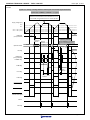
Figure 21-5. Incorrect description of voltage detector internal interrupt signal generation timing revised
(page 896)
Incorrect:
Figure 21-5. Timing of Voltage Detector Internal Interrupt Signal Generation
(Option Byte LVIMDS1, LVIMDS0 = 0, 1)
Supply voltage (VDD)
VLVI
VPOR = 1.51 V (TYP.)
VPDR = 1.50 V (TYP.)
Time
LVIMK flag
(set by software)
HNote 1
Cleared by
software
LVISEN flag
Cleared
LVIF flag
LVIOMSK flag
L
LVIMD flag
LVILV flag
H
INTLVI
LVIIF flag
Note 2
LVIRF flag
LVD reset signal
Cleared by
software
POR reset signal
Internal reset signal
Notes 1. The LVIMK flag is set to “1” by reset signal generation.
2. LVIRF flag is bit 0 of the reset control flag register (RESF).
The LVIRF flag may become 1 from the beginning due to the power-on waveform.
For details of the RESF register, see CHAPTER 19 RESET FUNCTION.
Page 28 of 70
RENESAS TECHNICAL UPDATE TN-RL*-A001C/E
Date: April. 6, 2012
Correct:
Figure 21-5. Timing of Voltage Detector Internal Interrupt Signal Generation
(Option Byte LVIMDS1, LVIMDS0 = 0, 1)
Supply voltage (VDD)
VLVI
VPOR = 1.51 V (TYP.)
VPDR = 1.50 V (TYP.)
Time
LVIMK flag
(interrupt mask)
(set by software)
H
Note
Cleared by
software
Cleared
LVIF flag
LVIMD flag
LVILV flag
H
INTLVI
LVIIF flag
LVD reset signal
POR reset signal
Internal reset signal
Note
The LVIMK flag is set to “1” by reset signal generation.
Page 29 of 70
RENESAS TECHNICAL UPDATE TN-RL*-A001C/E
Date: April. 6, 2012
9. Incorrect description of voltage detector (LVD) interrupt and reset mode revised
Incorrect description of when used as interrupt and reset mode revised (page 897)
Incorrect:
21.4.3 When used as interrupt and reset mode
• When starting operation
Specify the operation mode (the interrupt and reset (LVIMDS1, LVIMDS0 = 1, 0)) and the detection voltage
(VLVIH, VLVIL) by using the option byte 000C1H/010C1H.
(Omitted)
Figure 21-6 shows the timing of the internal reset signal and interrupt signal generated by the voltage detector.
Caution
The LVIRF flag may become 1 from the beginning due to the power-on waveform.
For details of the RESF register, see CHAPTER 19 RESET FUNCTION.
Correct:
21.4.3 When used as interrupt and reset mode
• When starting operation
Specify the operation mode (the interrupt and reset (LVIMDS1, LVIMDS0 = 1, 0)) and the detection voltage
(VLVIH, VLVIL) by using the option byte 000C1H/010C1H.
(Omitted)
Figures 21-6 shows the timing of voltage detector reset signal and interrupt signal generation.
Perform the processing according to figure 21-7 Processing procedure after an interrupt is generated and figure 21-8
Initial setting of interrupt and reset mode.
Page 30 of 70
RENESAS TECHNICAL UPDATE TN-RL*-A001C/E
Date: April. 6, 2012
Incorrect description of timing of voltage detector reset signal and interrupt signal generation revised
(page 898)
Incorrect:
Figure 21-6. Timing of Voltage Detector Reset Signal and Interrupt Signal Generation
(Option Byte LVIMDS1, LVIMDS0 = 1, 0)
Supply voltage (VDD)
VLVIH
VLVIL
VPOR = 1.51 V (TYP.)
VPDR = 1.50 V (TYP.)
Time
LVIMK flag
(set by software)
Note 1
Cleared by
software
Operation status
Normal
operation
RESET
RESET
Normal
operation
RESET
Save processing
LVIF flag
LVISEN flag
(set by software)
Cleared
LVIOMSK flag
LVIMD flag
LVILV flag
Note 2
LVIRF flag
Cleared
LVD reset signal
Cleared by
software
Cleared by
software
POR reset signal
Internal reset signal
INTLVI
LVIIF flag
Page 31 of 70
RENESAS TECHNICAL UPDATE TN-RL*-A001C/E
Date: April. 6, 2012
Notes 1. The LVIMK flag is set to “1” by reset signal generation.
2. LVIRF flag is bit 0 of the reset control flag register (RESF). The LVIRF flag may become 1 from the
beginning due to the power-on waveform. For details of the RESF register, see CHAPTER 19 RESET
FUNCTION.
Remark VPOR: POR power supply rise detection voltage
VPDR: POR power supply fall detection voltage
Page 32 of 70
RENESAS TECHNICAL UPDATE TN-RL*-A001C/E
Date: April. 6, 2012
Correct:
Figure 21-6. Timing of Voltage Detector Reset Signal and Interrupt Signal Generation
(Option Byte LVIMDS1, LVIMDS0 = 1, 0) (1/2)
If a reset is not generated after releasing the mask,
determine that a condition of VDD becomes VDD ≥ VLVIH,
clear LVIMD, and the MCU returns to normal operation.
Supply voltage (VDD)
VLVIH
VLVIL
VPOR = 1.51 V (TYP.)
VPDR = 1.50 V (TYP.)
LVIMK flag
(set by software)
Time
H Note 1
Cleared by
software
Operation status
RESET
Normal
operation
Normal
operation
Save
processing
Cleared by software
Wait for stabilization by software
(400 μs or 5 clocks of fIL) Note 3
RESET Normal operation
RESET
Save processing
Cleared
LVIF flag
LVISEN flag
(set by software)
LVIOMSK flag
LVIMD flag
Cleared by
software Note 3
LVILV flag
Cleared by
software Note 2
LVIRF flag
Cleared
LVD reset signal
POR reset signal
Internal reset signal
INTLVI
LVIIF flag
Page 33 of 70
RENESAS TECHNICAL UPDATE TN-RL*-A001C/E
Date: April. 6, 2012
Notes 1. The LVIMK flag is set to “1” by reset signal generation.
2. After an interrupt is generated, perform the processing according to figure 21-7 Processing Procedure After
an Interrupt Is Generated in interrupt and reset mode.
3. After a reset is released, perform the processing according to figure 21-8 Initial Setting of Interrupt and
Reset Mode in interrupt and reset mode.
Remark VPOR: POR power supply rise detection voltage
VPDR: POR power supply fall detection voltage
Page 34 of 70
RENESAS TECHNICAL UPDATE TN-RL*-A001C/E
Date: April. 6, 2012
Correct:
Figure 21-6. Timing of Voltage Detector Reset Signal and Interrupt Signal Generation
(Option Byte LVIMDS1, LVIMDS0 = 1, 0) (2/2)
When a condition of VDD is VDD < VLVIH after releasing the mask,
a reset is generated because of LVIMD = 1 (reset mode).
Supply voltage (VDD)
VLVIH
VLVIL
VPOR = 1.51 V (TYP.)
VPDR = 1.50 V (TYP.)
LVIMK flag
(set by software)
Time
H Note 1
Cleared by software
Wait for stabilization by software
(400 μs or 5 clocks of fIL)
Cleared by
software
Operation status
RESET
Save
Normal
operation processing
RESET
Normal operation
RESET
Save processing
Cleared
LVIF flag
LVISEN flag
(set by software)
LVIOMSK flag
LVIMD flag
Cleared by
software Note 3
LVILV flag
LVIRF flag
Cleared by
software Note 2
Cleared
LVD reset signal
POR reset signal
Internal reset signal
INTLVI
LVIIF flag
Page 35 of 70
RENESAS TECHNICAL UPDATE TN-RL*-A001C/E
Date: April. 6, 2012
Notes 1. The LVIMK flag is set to “1” by reset signal generation.
2. After an interrupt is generated, perform the processing according to figure 21-7 Processing Procedure After
an Interrupt Is Generated in interrupt and reset mode.
3. After a reset is released, perform the processing according to figure 21-8 Initial Setting of Interrupt and
Reset Mode in interrupt and reset mode.
Remark VPOR: POR power supply rise detection voltage
VPDR: POR power supply fall detection voltage
Page 36 of 70
RENESAS TECHNICAL UPDATE TN-RL*-A001C/E
Date: April. 6, 2012
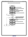
Figure 21-7. Processing Procedure After an Interrupt Is Generated
INTLVI generated
Save processing
Perform required save processing.
Set the LVISEN bit to 1 to mask voltage detection
LVISEN = 1
(LVIOMSK = 1).
Set the LVILV bit to 0 to set the high-voltage
LVILV = 0
LVISEN = 0
detection level (VLVIH).
Set the LVISEN bit to 0 to enable voltage detection.
LVIOMSK = 0
No
Yes
Yes
LVD reset
generated
No
Reset
The MCU returns to normal operation when
internal reset by voltage detector (LVD) is not
generated, since a condition of VDD becomes
VDD ≥ VLVIH.
LVISEN = 1
Set the LVISEN bit to 1 to mask voltage detection
(LVIOMSK = 1)
LVIMD = 0
Set the LVIMD bit to 0 to set interrupt mode.
LVISEN = 0
Set the LVISEN bit to 0 to enable voltage detection.
Normal operation
Page 37 of 70
RENESAS TECHNICAL UPDATE TN-RL*-A001C/E
Date: April. 6, 2012
Figure 21-8. Explanations of initial setting of interrupt and reset mode added (page 899)
When setting an interrupt and reset mode (LVIMDS1, LVIMDS0 = 1, 0), voltage detection stabilization wait time for 400 μs or 5
clocks of fIL is necessary after LVD reset is released (LVIRF = 1). After waiting until voltage detection stabilizes, (0) clear the
LVIMD bit for initialization. While voltage detection stabilization wait time is being counted and when the LVIMD bit is rewritten,
set LVISEN to 1 to mask a reset or interrupt generation by LVD.
Figure 21-8. shows the procedure for initial setting of interrupt and reset mode.
Figure 21-8. Initial Setting of Interrupt and Reset Mode
Power supply started
Reset source
determined
No
LVIRF = 1 ?
Refer to Figure 21-9. Checking reset source.
Check internal reset generation by LVD circuit
Yes
LVISEN = 1
Voltage detection
stabilization wait time
LVIMD = 0
LVISEN = 0
Set the LVISEN bit to 1 to mask voltage detection
(LVIOMSK = 1)
Count 400 μs or 5 clocks of fIL by software.
Set the LVIMD bit to 0 to set interrupt mode.
Set the LVISEN bit to 0 to enable voltage detection.
Normal operation
Remark fIL: Low-speed on-chip oscillator clock frequency
Page 38 of 70
RENESAS TECHNICAL UPDATE TN-RL*-A001C/E
Date: April. 6, 2012
10. Added common item for all RL78/G13 products in 29.4.2 Supply current characteristics of
Electrical specifications (page 1005)
Incorrect:
(4) Common to RL78/G13 all products
(TA = −40 to +85°C, 1.6 V ≤ EVDD0 = EVDD1 ≤ VDD ≤ 5.5 V, VSS = EVSS0 = EVSS1 = 0 V)
Parameter
Symbol
Notes 1, 2
RTC operating
current
IRTC
Watchdog timer
operating
current
IWDT
A/D converter
operating
current
IADC
Conditions
MIN.
fSUB = 32.768 kHz Real-time clock operation
TYP.
MAX.
Interval timer operation
Unit
μA
0.02
0.02
Notes 2,3
fIL = 15 kHz
0.22
Notes 4
When conversion Normal mode, AVREFP = VDD = 5.0 V
at maximum
Low voltage mode, AVREFP = VDD = 3.0 V
speed
1.3
1.7
mA
0.5
0.7
mA
Temperature
ITMPS
sensor operating
current
LVD operating ILVI Notes 5
μA
75
μA
0.08
μA
current
BGO operating
current
IBGO
Notes 6
2.50
12.20
mA
TYP.
MAX.
Unit
Note (Omitted)
Correct:
(4) Common to RL78/G13 all products
(TA = −40 to +85°C, 1.6 V ≤ EVDD0 = EVDD1 ≤ VDD ≤ 5.5 V, VSS = EVSS0 = EVSS1 = 0 V)
Parameter
Symbol
Notes 1, 2
RTC operating
current
IRTC
Watchdog timer
operating
current
IWDT
A/D converter
operating
current
IADC
A/D converter
reference
voltage current
IADREF
current
BGO operating
current
fSUB = 32.768 kHz Real-time clock operation
Interval timer operation
ILVI
MIN.
μA
0.02
0.02
Notes 2,3
fIL = 15 kHz
0.22
Notes 4
When conversion Normal mode, AVREFP = VDD = 5.0 V
at maximum
Low voltage mode, AVREFP = VDD = 3.0 V
speed
1.3
1.7
mA
0.5
0.7
mA
Temperature
ITMPS
sensor operating
current
LVD operating
Conditions
Notes 5
IBGO
Notes 6
μA
75
μA
75
μA
0.08
μA
2.50
12.20
mA
Note (Omitted)
Page 39 of 70
RENESAS TECHNICAL UPDATE TN-RL*-A001C/E
Date: April. 6, 2012
11. Explanations when using temperature sensor and internal reference voltage (1.45 V) of A/D
converter added
Explanation of Figure 11-7. A/D converter mode register 2 (ADM2) added (page 493)
Incorrect:
Figure 11-7.
Address: F0010H
Format of A/D Converter Mode Register 2 (ADM2) (1/2)
After reset: 00H
R/W
Symbol
7
6
5
4
<3>
<2>
1
<0>
ADM2
ADREFP1
ADREFP0
ADREFM
0
ADRCK
AWC
0
ADTYP
ADREFP1
ADREFP0
0
0
Supplied from VDD
0
1
Supplied from P20/AVREFP/ANI0
1
0
Supplied from the internal reference voltage (1.45 V)
1
1
Setting prohibited
Selection of the + side reference voltage source of the A/D converter
(Omitted)
(Omitted)
Correct:
Figure 11-7.
Address: F0010H
Format of A/D Converter Mode Register 2 (ADM2) (1/2)
After reset: 00H
R/W
Symbol
7
6
5
4
<3>
<2>
1
<0>
ADM2
ADREFP1
ADREFP0
ADREFM
0
ADRCK
AWC
0
ADTYP
ADREFP1
ADREFP0
0
0
Supplied from VDD
0
1
Supplied from P20/AVREFP/ANI0
1
0
Supplied from the internal reference voltage (1.45 V)
1
1
Setting prohibited
Selection of the + side reference voltage source of the A/D converter
Note
(Omitted)
Note This setting value can be selected only in HS (high-speed main) mode.
(Omitted)
Page 40 of 70
RENESAS TECHNICAL UPDATE TN-RL*-A001C/E
Date: April. 6, 2012
Explanation of Figure 11-11. Analog input channel specification register (ADS) added (page 496)
Incorrect:
Figure 11-11.
Format of Analog Input Channel Specification Register (ADS) (1/2)
{ Select mode (ADMD = 0)
ADISS
ADS4
ADS3
ADS2
ADS1
ADS0
Analog input
channel
Input source
0
0
0
0
0
0
ANI0
P20/ANI0/AVREFP pin
0
0
0
0
0
1
ANI1
P21/ANI1/AVREFM pin
0
1
1
0
1
1
Setting prohibited
1
0
0
0
0
0
−
Temperature sensor
output
1
0
0
0
0
1
−
Internal reference voltage
output (1.45 V)
(Omitted)
Other than the above
Notes
Setting prohibited
1. 20-, 24-, 25-, 30-, 32-pin products: P01/ANI16 pin
2. 20-, 24-, 25-, 30-, 32-pin products: P00/ANI17 pin
Correct:
Figure 11-11.
Format of Analog Input Channel Specification Register (ADS) (1/2)
{ Select mode (ADMD = 0)
ADISS
ADS4
ADS3
ADS2
ADS1
ADS0
Analog input
channel
Input source
0
0
0
0
0
0
ANI0
P20/ANI0/AVREFP pin
0
0
0
0
0
1
ANI1
P21/ANI1/AVREFM pin
Setting prohibited
(Omitted)
0
1
1
0
1
1
1
0
0
0
0
0
−
Temperature sensor
Note 3
output
1
0
0
0
0
1
−
Internal reference voltage
Note 3
output (1.45 V)
Other than the above
Notes
Setting prohibited
1. 20-, 24-, 25-, 30-, 32-pin products: P01/ANI16 pin
2. 20-, 24-, 25-, 30-, 32-pin products: P00/ANI17 pin
3. This setting value can be selected only in HS (high-speed main) mode.
Page 41 of 70
RENESAS TECHNICAL UPDATE TN-RL*-A001C/E
Date: April. 6, 2012
Explanation of 11.7.4 Setup when using temperature sensor added (page 523)
Incorrect:
11.7.4 Setup when using temperature sensor (example for software trigger mode and one-shot conversion mode)
Figure 11-35.
Setup When Using Temperature Sensor
(Omitted)
Note Depending on the settings of the ADRCK bit and ADUL/ADLL register, there is a possibility of no interrupt signal
being generated. In this case, the results are not stored in the ADCR, ADCRH registers.
Correct:
11.7.4 Setup when using temperature sensor (example for software trigger mode and one-shot conversion mode)
Figure 11-35.
Setup When Using Temperature Sensor
(Omitted)
Note Depending on the settings of the ADRCK bit and ADUL/ADLL register, there is a possibility of no interrupt signal
being generated. In this case, the results are not stored in the ADCR, ADCRH registers.
Caution
This setting can be used only in HS (high-speed main) mode.
Page 42 of 70
RENESAS TECHNICAL UPDATE TN-RL*-A001C/E
Date: April. 6, 2012
Explanation of (2) Input range of ANI0 to ANI14 and ANI16 to ANI26 pins in 11.10 Cautions for A/D
Converter added (page 530)
Incorrect:
11.10 Cautions for A/D Converter
(2) Input range of ANI0 to ANI14 and ANI16 to ANI26 pins
Observe the rated range of the ANI0 to ANI14 and ANI16 to ANI26 pins input voltage. If a voltage of VDD and AVREFP or
higher and VSS and AVREFM or lower (even in the range of absolute maximum ratings) is input to an analog input channel,
the converted value of that channel becomes undefined.
In addition, the converted values of the other channels may
also be affected.
When internal reference voltage (1.45 V) is selected reference voltage source for the + side of the A/D converter, do not
input internal reference voltage or higher voltage to a pin selected by the ADS register. However, it is no problem that a
pin not selected by the ADS register is inputed voltage greater than the internal reference voltage.
Correct:
11.10 Cautions for A/D Converter
(2) Input range of ANI0 to ANI14 and ANI16 to ANI26 pins
Observe the rated range of the ANI0 to ANI14 and ANI16 to ANI26 pins input voltage. If a voltage of VDD and AVREFP or
higher and VSS and AVREFM or lower (even in the range of absolute maximum ratings) is input to an analog input channel,
the converted value of that channel becomes undefined.
In addition, the converted values of the other channels may
also be affected.
When internal reference voltage (1.45 V) is selected reference voltage source for the + side of the A/D converter, do not
input internal reference voltage or higher voltage to a pin selected by the ADS register. However, it is no problem that a
pin not selected by the ADS register is inputed voltage greater than the internal reference voltage.
Caution
The internal reference voltage (1.45 V) can be selected only in HS (high-speed main) mode.
Page 43 of 70
RENESAS TECHNICAL UPDATE TN-RL*-A001C/E
Date: April. 6, 2012
12. Explanations of A/D test function in Safety functions chapter (section 22.3.8) added
Explanation of Figure 22-15. A/D test register (ADTES) added (page 917)
Incorrect:
(1) A/D test register (ADTES)
Figure 22-15.
Address: F0013H
After reset: 00H
R/W
Format of A/D Test Register (ADTES)
Symbol
7
6
5
4
3
2
1
0
ADTES
0
0
0
0
0
0
ADTES1
ADTES0
ADTES1
ADTES0
0
0
A/D conversion target
ANIxx (This is specified using the analog input channel specification register
(ADS).)
1
0
AVREFM
1
1
AVREFP
Other than the above
Setting prohibited
Correct:
(1) A/D test register (ADTES)
Figure 22-15.
Address: F0013H
After reset: 00H
R/W
Format of A/D Test Register (ADTES)
Symbol
7
6
5
4
3
2
1
0
ADTES
0
0
0
0
0
0
ADTES1
ADTES0
ADTES1
ADTES0
0
0
ANIxx (This is specified using the analog input channel specification register (ADS).)
1
0
AVREFM
1
1
AVREFP
Other than the above
A/D conversion target
Note
Setting prohibited
Note The temperature sensor output and internal reference voltage output (1.45 V) can be selected only in HS
(high-speed main) mode.
Page 44 of 70
RENESAS TECHNICAL UPDATE TN-RL*-A001C/E
Date: April. 6, 2012
Explanation of Figure 22-16. Analog input channel specification register (ADS) added (pages 918 to 919)
Incorrect:
Figure 22-16.
Format of Analog Input Channel Specification Register (ADS) (1/2)
{ Select mode (ADMD = 0)
ADISS
ADS4
ADS3
ADS2
ADS1
ADS0
Analog input
channel
Input source
0
0
0
0
0
0
ANI0
P20/ANI0/AVREFP pin
0
0
0
0
0
1
ANI1
P21/ANI1/AVREFM pin
0
1
1
0
1
1
Setting prohibited
1
0
0
0
0
0
−
Temperature sensor
output
1
0
0
0
0
1
−
Internal reference voltage
output (1.45 V)
(Omitted)
Other than the above
Setting prohibited
(Notes and cautions are listed on the next page.)
Notes 1.
20-, 24-, 25-, 30-, 32-pin products: P01/ANI16 pin
2.
20-, 24-, 25-, 30-, 32-pin products: P00/ANI17 pin
(Omitted)
Correct:
Figure 22-16.
Format of Analog Input Channel Specification Register (ADS) (1/2)
{ Select mode (ADMD = 0)
ADISS
ADS4
ADS3
ADS2
ADS1
ADS0
Analog input
channel
Input source
0
0
0
0
0
0
ANI0
P20/ANI0/AVREFP pin
0
0
0
0
0
1
ANI1
P21/ANI1/AVREFM pin
Setting prohibited
(Omitted)
0
1
1
0
1
1
1
0
0
0
0
0
−
Temperature sensor
Note 3
output
1
0
0
0
0
1
−
Internal reference voltage
Note 3
output (1.45 V)
Other than the above
Setting prohibited
(Notes and cautions are listed on the next page.)
Notes 1.
20-, 24-, 25-, 30-, 32-pin products: P01/ANI16 pin
2.
20-, 24-, 25-, 30-, 32-pin products: P00/ANI17 pin
3.
This setting value can be selected only in HS (high-speed main) mode.
(Omitted)
Page 45 of 70
RENESAS TECHNICAL UPDATE TN-RL*-A001C/E
Date: April. 6, 2012
13. Conditions of A/D converter characteristics in Electrical specifications chapter (section 29.7.1)
added
Condition of (1) When AVREF (+) = AVREFP/ANI0, AVREF (−) = AVREFM/ANI1, target ANI pin : ANI2 to
ANI14 added (page 1032)
Incorrect:
(1) When AVREF (+) = AVREFP/ANI0 (ADREFP1 = 0, ADREFP0 = 1), AVREF (−) = AVREFM/ANI1 (ADREFM = 1), target ANI pin :
ANI2 to ANI14
(TA = −40 to +85°C, 1.6 V ≤ EVDD0 = EVDD1 ≤ VDD ≤ 5.5 V, VSS = EVSS0 = EVSS1 = 0 V, Reference voltage (+) = AVREFP,
Reference voltage (−) = AVREFM = 0 V)
Parameter
Symbol
Resolution
Conditions
MIN.
RES
Notes 1, 2
Overall error
AINL
Conversion time
TYP.
8
MAX.
Unit
10
bit
10-bit resolution
1.8 V ≤ VDD ≤ 5.5 V
1.2
±3.5
LSB
AVREFP = VDD
1.6 V ≤ VDD ≤ 5.5 V
1.2
±7.0
LSB
1.6
VDD
V
0
AVREFP
V
1.5
V
tCONV
Notes 1, 2
Zero-scale error
EZS
(Omitted)
Notes 1, 2
Full-scale error
Integral linearity error
EFS
Note 1
Differential linearity error
Note 1
ILE
DLE
Reference voltage (+)
AVREFP
Analog input voltage
VAIN
VBGR
2.4 V ≤ VDD ≤ 5.5 V
1.38
1.45
(Omitted)
Page 46 of 70
RENESAS TECHNICAL UPDATE TN-RL*-A001C/E
Date: April. 6, 2012
Correct:
(1) When AVREF (+) = AVREFP/ANI0 (ADREFP1 = 0, ADREFP0 = 1), AVREF (−) = AVREFM/ANI1 (ADREFM = 1), target ANI pin :
ANI2 to ANI14
(TA = −40 to +85°C, 1.6 V ≤ EVDD0 = EVDD1 ≤ VDD ≤ 5.5 V, VSS = EVSS0 = EVSS1 = 0 V, Reference voltage (+) = AVREFP,
Reference voltage (−) = AVREFM = 0 V)
Parameter
Symbol
Resolution
Conditions
MIN.
RES
Notes 1, 2
Overall error
AINL
Conversion time
TYP.
8
MAX.
Unit
10
bit
10-bit resolution
1.8 V ≤ VDD ≤ 5.5 V
1.2
±3.5
LSB
AVREFP = VDD
1.6 V ≤ VDD ≤ 5.5 V
1.2
±7.0
LSB
1.6
VDD
V
0
AVREFP
V
1.5
V
tCONV
Notes 1, 2
Zero-scale error
EZS
(Omitted)
Notes 1, 2
Full-scale error
Integral linearity error
EFS
Note 1
Differential linearity error
Note 1
ILE
DLE
Reference voltage (+)
AVREFP
Analog input voltage
VAIN
VBGR
2.4 V ≤ VDD ≤ 5.5 V
HS mode
1.38
1.45
(Omitted)
Page 47 of 70
RENESAS TECHNICAL UPDATE TN-RL*-A001C/E
Date: April. 6, 2012
Condition of (2) When AVREF (+) = AVREFP/ANI0, AVREF (−) = AVREFM/ANI1, target ANI pin : ANI16 to
ANI26 added (page 1033)
Incorrect:
(2) When AVREF (+) = AVREFP/ANI0 (ADREFP1 = 0, ADREFP0 = 1), AVREF (−) = AVREFM/ANI1 (ADREFM = 1), target ANI pin :
ANI16 to ANI26
(TA = −40 to +85°C, 1.6 V ≤ EVDD0 = EVDD1 ≤ VDD ≤ 5.5 V, VSS = EVSS0 = EVSS1 = 0 V, Reference voltage (+) = AVREFP,
Reference voltage (−) = AVREFM)
Parameter
Symbol
Resolution
Conditions
MIN.
RES
Notes 1, 2
Overall error
AINL
Conversion time
8
MAX.
Unit
10
bit
10-bit resolution
1.8 V ≤ VDD ≤ 5.5 V
1.2
±5.0
LSB
AVREFP = VDD
1.6 V ≤ VDD ≤ 5.5 V
1.2
±8.5
LSB
1.6
VDD
V
0
AVREFP
V
tCONV
Notes 1, 2
Zero-scale error
EZS
Notes 1, 2
Full-scale error
Integral linearity error
TYP.
Note 1
Differential linearity error
(Omitted)
EFS
Note 1
ILE
DLE
Reference voltage (+)
AVREFP
Analog input voltage
VAIN
and
EVDD0
VBGR
2.4 V ≤ VDD ≤ 5.5 V
1.38
1.45
1.5
V
(Omitted)
Page 48 of 70
RENESAS TECHNICAL UPDATE TN-RL*-A001C/E
Date: April. 6, 2012
Correct:
(2) When AVREF (+) = AVREFP/ANI0 (ADREFP1 = 0, ADREFP0 = 1), AVREF (−) = AVREFM/ANI1 (ADREFM = 1), target ANI pin :
ANI16 to ANI26
(TA = −40 to +85°C, 1.6 V ≤ EVDD0 = EVDD1 ≤ VDD ≤ 5.5 V, VSS = EVSS0 = EVSS1 = 0 V, Reference voltage (+) = AVREFP,
Reference voltage (−) = AVREFM)
Parameter
Symbol
Resolution
Conditions
MIN.
RES
Notes 1, 2
Overall error
AINL
Conversion time
8
MAX.
Unit
10
bit
10-bit resolution
1.8 V ≤ VDD ≤ 5.5 V
1.2
±5.0
LSB
AVREFP = VDD
1.6 V ≤ VDD ≤ 5.5 V
1.2
±8.5
LSB
1.6
VDD
V
0
AVREFP
V
tCONV
Notes 1, 2
Zero-scale error
EZS
Notes 1, 2
Full-scale error
Integral linearity error
TYP.
Note 1
Differential linearity error
(Omitted)
EFS
Note 1
ILE
DLE
Reference voltage (+)
AVREFP
Analog input voltage
VAIN
and
EVDD0
VBGR
2.4 V ≤ VDD ≤ 5.5 V
HS mode
1.38
1.45
1.5
V
(Omitted)
Page 49 of 70
RENESAS TECHNICAL UPDATE TN-RL*-A001C/E
Date: April. 6, 2012
Condition of (3) When AVREF (+) = VDD, AVREF (−) = VSS, target ANI pin : ANI0 to ANI14, ANI16 to ANI26
added (page 1034)
Incorrect:
(3) When AVREF (+) = VDD (ADREFP1 = 0, ADREFP0 = 0), AVREF (−) = VSS (ADREFM = 0), target ANI pin : ANI0 to ANI14,
ANI16 to ANI26
(TA = −40 to +85°C, 1.6 V ≤ EVDD0 = EVDD1 ≤ VDD ≤ 5.5 V, VSS = EVSS0 = EVSS1 = 0 V, Reference voltage (+) = VDD, Reference
voltage (−) = VSS)
Parameter
Symbol
Resolution
Conditions
MIN.
RES
Notes 1, 2
Overall error
AINL
Conversion time
Notes 1, 2
10-bit resolution
Unit
10
bit
1.8 V ≤ VDD ≤ 5.5 V
1.2
±7.0
LSB
1.6 V ≤ VDD ≤ 5.5 V
1.2
±10.5
LSB
Notes 1, 2
EFS
Note 1
Differential linearity error
(Omitted)
EZS
Full-scale error
Analog input voltage
8
MAX.
tCONV
Zero-scale error
Integral linearity error
TYP.
Note 1
ILE
DLE
VAIN
VBGR
ANI0 to ANI14
0
VDD
V
ANI16 to ANI26
0
EVDD0
V
1.5
V
2.4 V ≤ VDD ≤ 5.5 V
1.38
1.45
(Omitted)
Page 50 of 70
RENESAS TECHNICAL UPDATE TN-RL*-A001C/E
Date: April. 6, 2012
Correct:
(3) When AVREF (+) = VDD (ADREFP1 = 0, ADREFP0 = 0), AVREF (−) = VSS (ADREFM = 0), target ANI pin : ANI0 to ANI14,
ANI16 to ANI26
(TA = −40 to +85°C, 1.6 V ≤ EVDD0 = EVDD1 ≤ VDD ≤ 5.5 V, VSS = EVSS0 = EVSS1 = 0 V, Reference voltage (+) = VDD, Reference
voltage (−) = VSS)
Parameter
Symbol
Resolution
Conditions
MIN.
RES
Notes 1, 2
Overall error
AINL
Conversion time
Notes 1, 2
10-bit resolution
Unit
10
bit
1.8 V ≤ VDD ≤ 5.5 V
1.2
±7.0
LSB
1.6 V ≤ VDD ≤ 5.5 V
1.2
±10.5
LSB
Notes 1, 2
EFS
Note 1
Differential linearity error
(Omitted)
EZS
Full-scale error
Analog input voltage
8
MAX.
tCONV
Zero-scale error
Integral linearity error
TYP.
Note 1
ILE
DLE
VAIN
VBGR
ANI0 to ANI14
0
VDD
V
ANI16 to ANI26
0
EVDD0
V
1.5
V
2.4 V ≤ VDD ≤ 5.5 V
HS mode
1.38
1.45
(Omitted)
Page 51 of 70
RENESAS TECHNICAL UPDATE TN-RL*-A001C/E
Date: April. 6, 2012
Condition of (4) When AVREF (+) = Internal reference voltage, AVREF (−) = AVREFM/ANI1, target ANI pin :
ANI0 to ANI14, ANI16 to ANI26 added (page 1035)
Incorrect:
(4) When AVREF (+) = Internal reference voltage (ADREFP1 = 1, ADREFP0 = 0), AVREF (−) = AVREFM/ANI1 (ADREFM = 1),
target ANI pin : ANI0 to ANI14, ANI16 to ANI26
(TA = −40 to +85°C, 1.6 V ≤ EVDD0 = EVDD1 ≤ VDD ≤ 5.5 V, VSS = EVSS0 = EVSS1 = 0 V, Reference voltage (+) = VBGR, Reference
voltage (−) = AVREFM = 0 V)
Parameter
Symbol
Resolution
Conditions
MIN.
RES
Conversion time
Notes 1, 2
Zero-scale error
Integral linearity error
Note 1
Differential linearity error
Note 1
TYP.
MAX.
8
Unit
bit
tCONV
8-bit resolution
2.4 V ≤ VDD ≤ 5.5 V
39
μs
EZS
8-bit resolution
2.4 V ≤ VDD ≤ 5.5 V
±0.60
%FSR
ILE
8-bit resolution
2.4 V ≤ VDD ≤ 5.5 V
±2.0
LSB
DLE
8-bit resolution
2.4 V ≤ VDD ≤ 5.5 V
±1.0
LSB
1.5
V
Reference voltage (+)
VBGR
Reference voltage (−)
AVREFM
Analog input voltage
VAIN
17
1.38
1.45
VSS
0
V
VBGR
V
(Omitted)
Correct:
(4) When AVREF (+) = Internal reference voltage (ADREFP1 = 1, ADREFP0 = 0), AVREF (−) = AVREFM/ANI1 (ADREFM = 1),
target ANI pin : ANI0 to ANI14, ANI16 to ANI26
(TA = −40 to +85°C, 2.4 V ≤ VDD ≤ 5.5 V, VSS = EVSS0 = EVSS1 = 0 V, Reference voltage (+) = VBGR, Reference voltage (−) =
AVREFM = 0 V, HS (high-speed main) mode)
Parameter
Symbol
Resolution
Conditions
MIN.
RES
Conversion time
Notes 1, 2
Zero-scale error
Integral linearity error
Note 1
Differential linearity error
Note 1
2.4 V ≤ VDD ≤ 5.5 V
±0.60
%FSR
8-bit resolution
2.4 V ≤ VDD ≤ 5.5 V
±2.0
LSB
8-bit resolution
2.4 V ≤ VDD ≤ 5.5 V
±1.0
LSB
1.5
V
EZS
8-bit resolution
ILE
DLE
AVREFM
Analog input voltage
VAIN
bit
μs
2.4 V ≤ VDD ≤ 5.5 V
Reference voltage (−)
Unit
39
8-bit resolution
VBGR
MAX.
8
tCONV
Reference voltage (+)
TYP.
17
1.38
1.45
VSS
0
V
VBGR
V
(Omitted)
Page 52 of 70
RENESAS TECHNICAL UPDATE TN-RL*-A001C/E
Date: April. 6, 2012
14. Condition of Temperature sensor characteristics in Electrical Specifications chapter (section
29.7.2) added (page 1036)
Incorrect:
29.7.2 Temperature sensor characteristics
(TA = −40 to +85°C, 2.4 V ≤ EVDD0 = EVDD1 ≤ VDD ≤ 5.5 V, VSS = EVSS0 = EVSS1 = 0 V)
Parameter
Symbol
Conditions
Temperature sensor output voltage VTMPS25
Setting ADS register = 80H, TA = +25°C
Reference output voltage
VCONST
Setting ADS register = 81H
Temperature coefficient
FVTMPS
Temperature sensor that depends on the
MIN.
TYP.
MAX.
1.05
1.38
1.45
Unit
V
1.5
−3.6
V
mV/C
temperature
Operation stabilization wait time
tAMP
5
μs
MAX.
Unit
1.5
V
Correct:
29.7.2 Temperature sensor characteristics
(TA = −40 to +85°C, 2.4 V ≤ VDD ≤ 5.5 V, VSS = EVSS0 = EVSS1 = 0 V, HS (high-speed main) mode)
Parameter
Symbol
Conditions
Temperature sensor output voltage VTMPS25
Setting ADS register = 80H, TA = +25°C
Reference output voltage
VCONST
Setting ADS register = 81H
Temperature coefficient
FVTMPS
Temperature sensor that depends on the
MIN.
TYP.
1.38
1.45
1.05
V
−3.6
mV/C
temperature
Operation stabilization wait time
tAMP
5
μs
Page 53 of 70
RENESAS TECHNICAL UPDATE TN-RL*-A001C/E
Date: April. 6, 2012
15. Industrial applications and extended-temperature products released
Industrial applications and extended-temperature products released (p.5)
Added:
Figure 1-1. Part Number, Memory Size, and Package of RL78/G13
Part No. R 5 F 1 0 0 L E A x x x F B
Package type:
SP : SSOP, 0.65 mm pitch
FP : LQFP, 0.80 mm pitch
FA : LQFP, 0.65 mm pitch
FB : LQFP, 0.50 mm pitch
NA : WQFN, 0.50 mm pitch
LA : LGA, 0.50 mm pitch
BG : FBGA, 0.40 mm pitch
ROM number (Omitted with blank products)
Classification:
A : Consumer applications, operating ambient temperature : -40˚C to 85˚C
D : Industrial applications, operating ambient temperature : -40˚C to 85˚C
ROM capacity:
A : 16 KB
C : 32 KB
D : 48 KB
E : 64 KB
F : 96 KB
G : 128 KB
H : 192 KB
J : 256 KB
K : 384 KB
L : 512 KB
Pin count:
A :
B :
C :
E :
F :
G:
J :
L :
M:
P :
S :
20 to 30-pin
32-pin
36-pin
40-pin
44-pin
48-pin
52-pin
64-pin
80-pin
100-pin
128-pin
RL78/G13 group
100 : Data flash is provided
101 : Data flash is not provided
Memory type:
F : Flash memory
Renesas MCU
Renesas semiconductor product
Remark
For details about extended-temperature products (operating ambient temperature: −40°C to 105°C), contact a
Renesas Electronics Corporation or an authorized Renesas Electronics Corporation distributor.
Page 54 of 70
RENESAS TECHNICAL UPDATE TN-RL*-A001C/E
Date: April. 6, 2012
IOH spec of products for industrial application in DC characteristics of ELECTRICAL SPECIFICATIONS
added (p.988)
Incorrect:
29.4.1 Pin characteristics
(TA = −40 to +85°C, 1.6 V ≤ EVDD0 = EVDD1 ≤ VDD ≤ 5.5 V, VSS = EVSS0 = EVSS1 = 0 V)
Items
Output current,
Note 1
high
Symbol
IOH1
Conditions
MIN.
TYP.
MAX.
Unit
−10.0
mA
Per pin for P00 to P07, P10 to P17,
P30 to P37, P40 to P47, P50 to P57,
P64 to P67, P70 to P77, P80 to P87,
P90 to P97, P100 to P106,
P110 to P117, P120, P125 to P127,
P130, P140 to P147
1.6 V ≤ EVDD0 ≤ 5.5 V
Total of all pins
Note 3
)
(When duty = 70%
1.6 V ≤ EVDD0 ≤ 5.5 V
−135.0
mA
Per pin for P20 to P27, P150 to P156
1.6 V ≤ VDD ≤ 5.5 V
−0.1
Note
mA
Note 2
(Omitted)
IOH2
2
1.6 V ≤ VDD ≤ 5.5 V
Total of all pins
Note 3
(When duty = 70%
)
Notes 1.
−1.5
mA
Value of current at which the device operation is guaranteed even if the current flows from the EVDD0, EVDD1,
VDD pins to an output pin.
(Omitted)
Correct:
29.3.1 Pin characteristics
(TA = −40 to +85°C, 1.6 V ≤ EVDD0 = EVDD1 ≤ VDD ≤ 5.5 V, VSS = EVSS0 = EVSS1 = 0 V)
Items
Output current,
Note 1
high
Symbol
IOH1
Conditions
Per pin for P00 to P07, P10 to P17,
P30 to P37, P40 to P47, P50 to P57,
P64 to P67, P70 to P77, P80 to P87,
P90 to P97, P100 to P106,
P110 to P117, P120, P125 to P127,
P130, P140 to P147
MIN.
1.6 V ≤ EVDD0 ≤ 5.5 V
TYP.
MAX.
Unit
−10.0
mA
Note 2
(Omitted)
IOH2
Total of all pins
Note 3
)
(When duty = 70%
1.6 V ≤ EVDD0 ≤ 5.5 V
Per pin for P20 to P27, P150 to P156
1.6 V ≤ VDD ≤ 5.5 V
−135.0
mA
Note 4
−0.1
Note
mA
2
Total of all pins
Note 3
)
(When duty = 70%
Notes 1.
1.6 V ≤ VDD ≤ 5.5 V
−1.5
mA
Value of current at which the device operation is guaranteed even if the current flows from the EVDD0, EVDD1,
VDD pins to an output pin.
(Omitted)
4.
The applied current for the products for industrial application (R5F100xxDxx, R5F101xxDxx) is −100 mA.
Page 55 of 70
RENESAS TECHNICAL UPDATE TN-RL*-A001C/E
Date: April. 6, 2012
16. Incorrect descriptions of recommended connection of unused pins of P60 to P63 in table 2-3 in pin
functions chapter revised (p.93)
Incorrect:
Table 2-3. Connection of Unused Pins (128-pin products) (2/4)
Pin Name
I/O Circuit Type
I/O
Recommended Connection of Unused Pins
(Omitted)
P60/SCLA0
13-R
I/O
Input:
Independently connect to EVDD0, EVDD1 or EVSS0, EVSS1
via a resistor.
P61/SDAA0
Output: Leave open.
P62/SCLA1
P63/SDAA1
P64/TI10/TO10
8-R
P65/TI11/TO11
P66/TI12/TO12
P67/TI13/TO13
Correct:
Table 2-3. Connection of Unused Pins (128-pin products) (2/4)
Pin Name
I/O Circuit Type
I/O
Recommended Connection of Unused Pins
(Omitted)
P60/SCLA0
13-R
I/O
Input:
Independently connect to EVDD0, EVDD1 or EVSS0, EVSS1
via a resistor.
P61/SDAA0
Output: Set the port’s output latch to 0 and leave the pins open,
P62/SCLA1
or set the port’s output latch to 1 and independently
P63/SDAA1
connect the pins to EVDD0 and EVDD1 or EVSS0 and EVSS1
via a resistor.
P64/TI10/TO10
8-R
Input:
P65/TI11/TO11
P66/TI12/TO12
Independently connect to EVDD0, EVDD1 or EVSS0, EVSS1
via a resistor.
Output:
Leave open.
P67/TI13/TO13
Page 56 of 70
RENESAS TECHNICAL UPDATE TN-RL*-A001C/E
Date: April. 6, 2012
17. Incorrect descriptions of 7.4.2 Shifting to HALT/STOP mode after starting operation in real-time
clock chapter revised (p.449)
Incorrect:
7.4.2 Shifting to STOP mode after starting operation
Perform one of the following processing when shifting to STOP mode immediately after setting the RTCE bit to 1.
However, after setting the RTCE bit to 1, this processing is not required when shifting to STOP mode after the INTRTC
interrupt has occurred.
• Shifting to STOP mode when at least two input clocks (fRTC) have elapsed after setting the RTCE bit to 1 (see Figure 7-18,
Example 1).
• Checking by polling the RWST bit to become 1, after setting the RTCE bit to 1 and then setting the RWAIT bit to 1.
Afterward, setting the RWAIT bit to 0 and shifting to STOP mode after checking again by polling that the RWST bit has
become 0 (see Figure 7-18, Example 2).
Figure 7-18.
Procedure for Shifting to STOP Mode After Setting RTCE bit to 1
Example 1
RTCE = 1
Example 2
RTCE = 1
Sets to counter operation
start
Waiting at least for 2
fRTC clocks
STOP instruction execution
Shifts to STOP mode
No
Sets to counter operation
start
RWAIT = 1
Sets to stop the SEC to YEAR
counters, reads the counter
value, write mode
RWST = 1 ?
Checks the counter wait status
Yes
RWAIT = 0
No
Sets the counter operation
RWST = 0 ?
Yes
STOP instruction execution
Shifts to STOP mode
Page 57 of 70
RENESAS TECHNICAL UPDATE TN-RL*-A001C/E
Date: April. 6, 2012
Correct:
7.4.2 Shifting to HALT/STOP mode after starting operation
Perform one of the following processing when shifting to HALT/STOP mode immediately after setting the RTCE bit to 1.
However, after setting the RTCE bit to 1, this processing is not required when shifting to HALT/STOP mode after the
INTRTC interrupt has occurred.
• Shifting to HALT/STOP mode when at least two input clocks (fRTC) have elapsed after setting the RTCE bit to 1 (see
Figure 7-18, Example 1).
• Checking by polling the RWST bit to become 1, after setting the RTCE bit to 1 and then setting the RWAIT bit to 1.
Afterward, setting the RWAIT bit to 0 and shifting to HALT/STOP mode after checking again by polling that the RWST bit
has become 0 (see Figure 7-18, Example 2).
Figure 7-18.
Procedure for Shifting to HALT/STOP Mode After Setting RTCE bit to 1
Example 1
RTCE = 1
Example 2
Sets to counter operation
start
Waiting at least for 2
fRTC clocks
HALT/STOP instruction
execution
Shifts to HALT/STOP mode
No
RTCE = 1
Sets to counter operation
start
RWAIT = 1
Sets to stop the SEC to YEAR
counters, reads the counter
value, write mode
RWST = 1?
Checks the counter wait status
Yes
RWAIT = 0
No
Sets the counter operation
RWST = 0 ?
Yes
HALT/STOP instruction
eaxecution
Shifts to HALT/STOP mode
Page 58 of 70
RENESAS TECHNICAL UPDATE TN-RL*-A001C/E
Date: April. 6, 2012
18. Incorrect descriptions of reset processing time/standby mode release time revised
Incorrect descriptions of reset processing time revised (p.308, 861, 866, 871, 872, 883, 884)
Incorrect:
Reset processing time of reset by POR when the power is turned on
Reset processing time: 387 to 720 μ s (When LVD is used)
155 to 407 μ s (When LVD off)
Reset processing time when HALT reset or STOP reset
Reset processing time: 387 to 720 μ s (When LVD is used)
155 to 407 μ s (When LVD off)
Reset processing time when RESET input
Reset processing time: 387 to 674 μ s (When LVD is used)
155 to 360 μ s (When LVD off)
Correct:
Reset processing time of reset by POR when the power is turned on
Reset processing time: 497 to 720 μ s (When LVD is used)
265 to 407 μ s (When LVD off)
Reset processing time when HALT reset or STOP reset or RESET input
Reset processing time: 388 to 673 μ s (When LVD is used)
156 to 360 μ s (When LVD off)
Page 59 of 70
RENESAS TECHNICAL UPDATE TN-RL*-A001C/E
Date: April. 6, 2012
Incorrect descriptions of HALT mode release time revised (p.860)
Incorrect:
Figure 18-3.
HALT Mode Release by Interrupt Request Generation
HALT
instruction
Interrupt
request
Standby
release signal
Status of CPU
Operating mode
Operating mode
Oscillation
High-speed system clock,
High-speed on-chip oscillator clock,
or subsystem clock
Note
Wait Note
HALT mode
Wait time for HALT mode release
• When vectored interrupt servicing is carried out
Main system clock:
13 to 15 clock
Subsystem clock (RTCLPC = 0): 8 to 10 clock
Subsystem clock (RTCLPC = 1): 9 to 11 clock
• When vectored interrupt servicing is not carried out
Main system clock:
8 to 9 clock
Subsystem clock (RTCLPC = 0): 3 to 4 clock
Subsystem clock (RTCLPC = 1): 4 to 5 clock
Correct:
Figure 18-3.
HALT Mode Release by Interrupt Request Generation
HALT
instruction
Interrupt
request
Standby
release signal Note 1
Status of CPU
Operating mode
2.
Operating mode
Oscillation
High-speed system clock,
High-speed on-chip oscillator clock,
or subsystem clock
Notes 1.
Wait Note 2
HALT mode
For details of the standby release signal, see Figure 16-1
Wait time for HALT mode release
• When vectored interrupt servicing is carried out
Main system clock:
15 to 16 clock
Subsystem clock (RTCLPC = 0): 10 to 11 clock
Subsystem clock (RTCLPC = 1): 11 to 12 clock
• When vectored interrupt servicing is not carried out
Main system clock:
9 to 10 clock
Subsystem clock (RTCLPC = 0):
4 to 5 clock
Subsystem clock (RTCLPC = 1):
5 to 6 clock
Page 60 of 70
RENESAS TECHNICAL UPDATE TN-RL*-A001C/E
Date: April. 6, 2012
Incorrect descriptions of STOP mode release time revised (p.864, 865)
Incorrect:
Figure 18-5.
STOP Mode Release by Interrupt Request Generation (1/2)
(1) When high-speed system clock (X1 oscillation) is used as CPU clock
Interrupt
request
STOP
instruction
Standby release signal
Status of CPU
High-speed
system clock
(X1 oscillation)
Note
Normal operation
(high-speed
system clock)
STOP mode
Oscillates
Oscillation stopped
Oscillation
stabilization time
(set by OSTS)
Wait
Normal operation
(high-speed
system clock)
Note
Oscillates
Wait time for STOP mode release
• High-speed system clock (X1 oscillation): 3-clock
Figure 18-5.
STOP Mode Release by Interrupt Request Generation (2/2)
(2) When high-speed system clock (external clock input) is used as CPU clock
Interrupt
request
STOP
instruction
Standby release signal
Status of CPU
High-speed
system clock
(external clock input)
STOP mode release tuime Note
Supply of the
Wait
clock is stopped
Normal operation
(high-speed
system clock)
STOP mode
Oscillates
Oscillation stopped
Normal operation
(high-speed
system clock)
Oscillates
(3) When high-speed on-chip oscillator clock is used as CPU clock
(Omitted)
Note
STOP mode release time:
• High-speed system clock (external clock input): 19.1 to 31.98 μ s
• High-speed on-chip oscillator clock:
19.1 to 31.98 μs
Page 61 of 70
RENESAS TECHNICAL UPDATE TN-RL*-A001C/E
Date: April. 6, 2012
Correct:
Figure 18-5.
STOP Mode Release by Interrupt Request Generation (1/2)
(1) When high-speed system clock (X1 oscillation) is used as CPU clock
STOP
instruction
Interrupt
request
Standby release signal Note 1
Status of CPU
High-speed
system clock
(X1 oscillation)
Notes 1.
2.
STOP mode release time Note 2
Normal operation
(high-speed
system clock)
STOP mode
Oscillates
Oscillation stopped
Supply of the
clock is stopped
Wait
Normal operation
(high-speed
system clock)
Oscillates
For details of the standby release signal, see Figure 16-1
STOP mode release time
Supply of the clock is stopped: 18.96 μ s to “whichever is longer 28.95 μ s and the oscillation
stabilization time (set by OSTS)”
Wait
• When vectored interrupt servicing is carried out:
10 to 11 clocks
• When vectored interrupt servicing is not carried out: 4 to 5 clocks
Figure 18-5.
STOP Mode Release by Interrupt Request Generation (2/2)
(2) When high-speed system clock (external clock input) is used as CPU clock
STOP
instruction
Interrupt
request
Standby release signal Note 1
Status of CPU
High-speed
system clock
(X1 oscillation)
STOP mode release time Note 2
Normal operation
(high-speed
system clock)
STOP mode
Oscillates
Oscillation stopped
Supply of the
clock is stopped
Wait
Normal operation
(high-speed
system clock)
Oscillates
(3) When high-speed on-chip oscillator clock is used as CPU clock
(Omitted)
Notes 1.
2.
For details of the standby release signal, see Figure 16-1
STOP mode release time
Supply of the clock is stopped: 19.08 to 32.99 μ s
Wait
• When vectored interrupt servicing is carried out:
7 clocks
• When vectored interrupt servicing is not carried out: 1 clock
Page 62 of 70
RENESAS TECHNICAL UPDATE TN-RL*-A001C/E
Date: April. 6, 2012
Explanations of SNOOZE mode shift time added (p.867)
Incorrect:
18.2.3 SNOOZE mode
(1) SNOOZE mode setting and operating statuses
(Omitted)
Correct:
18.2.3 SNOOZE mode
(1) SNOOZE mode setting and operating statuses
(Omitted)
In SNOOZE mode transition, wait status to be only following time.
From STOP to SNOOZE
HS (High-speed main) mode : 18.96 to 28.95 μ s
LS (Low-speed main) mode :
20.24 to 28.95 μ s
LV (Low-voltage main) mode : 20.98 to 28.95 μ s
From SNOOZE to normal operation
• When vectored interrupt servicing is carried out:
HS (High-speed main) mode :
6.79 to 12.4 μ s + 7 clocks
LS (Low-speed main) mode :
2.58 to 7.8 μ s + 7 clocks
LV (Low-voltage main) mode :
12.45 to 17.3 μ s + 7 clocks
• When vectored interrupt servicing is not carried out:
HS (High-speed main) mode :
6.79 to 12.4 μ s + 1 clock
LS (Low-speed main) mode :
2.58 to 7.8 μ s + 1 clock
LV (Low-voltage main) mode :
12.45 to 17.3 μ s + 1 clock
Page 63 of 70
RENESAS TECHNICAL UPDATE TN-RL*-A001C/E
Date: April. 6, 2012
19. Explanations of when using SNOOZE mode in A/D converter chapter added
Explanations of A/D converter mode register 2 (ADM2) added (p.493, 494)
Incorrect:
(4) A/D converter mode register 2 (ADM2)
(Omitted)
ADREFP1
ADREFP0
Selection of the + side reference voltage source of the A/D converter
0
0
Supplied from VDD
0
1
Supplied from P20/AVREFP/ANI0
1
0
Supplied from the internal reference voltage (1.45 V)
1
1
Setting prohibited
・ When ADREFP1 or ADREFP0 bit is rewritten, this must be configured in accordance with the following procedures.
(1) Set ADCE = 0
(2) Change the values of ADREFP1 and ADREFP0
(3) Stabilization wait time (A)
(4) Set ADCE = 1
(5) Stabilization wait time (B)
When ADREFP1 and ADREFP0 are set to 1 and 0, the setting is changed to A = 1 μ s, B = 5 μ s.
When ADREFP1 and ADREFP0 are set to 0 and 0 or 0 and 1, A needs no wait and B = 1 μ s.
・ When ADREFP1 and ADREFP0 are set to 1 and 0, respectively, A/D conversion cannot be performed on the
temperature sensor output.
Be sure to perform A/D conversion while ADISS = 0.
AWC
Specification of the SNOOZE mode
0
Do not use the SNOOZE mode function.
1
Use the SNOOZE mode function.
When there is a hardware trigger signal in the STOP mode, the STOP mode is exited, and A/D conversion is performed
without operating the CPU (the SNOOZE mode).
• The SNOOZE mode function can only be specified when the high-speed on-chip oscillator clock is selected for the
CPU/peripheral hardware clock (fCLK).
If any other clock is selected, specifying this mode is prohibited.
• Using the SNOOZE mode function in the software trigger mode or hardware trigger no-wait mode is prohibited.
• Using the SNOOZE mode function in the sequential conversion mode is prohibited.
• When using the SNOOZE mode function, specify a hardware trigger interval of at least “A/D conversion time
with stabilization wait time” listed for Table 11-3.
Page 64 of 70
RENESAS TECHNICAL UPDATE TN-RL*-A001C/E
Date: April. 6, 2012
Correct:
(4) A/D converter mode register 2 (ADM2)
(Omitted)
ADREFP1
ADREFP0
Selection of the + side reference voltage source of the A/D converter
0
0
Supplied from VDD
0
1
Supplied from P20/AVREFP/ANI0
1
0
Supplied from the internal reference voltage (1.45 V)
1
1
Setting prohibited
Note
• When ADREFP1 or ADREFP0 bit is rewritten, this must be configured in accordance with the following procedures.
(1) Set ADCE = 0
(2) Change the values of ADREFP1 and ADREFP0
(3) Stabilization wait time (A)
(4) Set ADCE = 1
(5) Stabilization wait time (B)
When ADREFP1 and ADREFP0 are set to 1 and 0, the setting is changed to A = 5 μ s, B = 1 μ s.
When ADREFP1 and ADREFP0 are set to 0 and 0 or 0 and 1, A needs no wait and B = 1 μ s.
After (5) stabilization time, start the A/D conversion.
• When ADREFP1 and ADREFP0 are set to 1 and 0, respectively, A/D conversion cannot be performed on the
temperature sensor output and internal reference voltage output.
Be sure to perform A/D conversion while ADISS = 0.
AWC
Specification of the SNOOZE mode
0
Do not use the SNOOZE mode function.
1
Use the SNOOZE mode function.
When there is a hardware trigger signal in the STOP mode, the STOP mode is exited, and A/D conversion is performed
without operating the CPU (the SNOOZE mode).
• The SNOOZE mode function can only be specified when the high-speed on-chip oscillator clock is selected for the
CPU/peripheral hardware clock (fCLK). If any other clock is selected, specifying this mode is prohibited.
• Using the SNOOZE mode function in the software trigger mode or hardware trigger no-wait mode is prohibited.
• Using the SNOOZE mode function in the sequential conversion mode is prohibited.
• When using the SNOOZE mode function, specify a hardware trigger interval of at least “shift time to SNOOZE mode
Note
+ A/D power supply stabilization wait time + A/D conversion time +2 fCLK clock”
• Even when using SNOOZE mode, be sure to set the AWC bit to 0 in normal operation mode and change it to 1 just
before shifting to STOP mode.
Also, be sure to change the AWC bit to 0 after returning from STOP mode to normal operation mode.
If the AWC bit is left set to 1, A/D conversion will not start normally in spite of the subsequent SNOOZE or normal
operation mode.
Note
Refer to “From STOP to SNOOZE” in 18.2.3 SNOOZE mode
Page 65 of 70
RENESAS TECHNICAL UPDATE TN-RL*-A001C/E
Date: April. 6, 2012
Explanations of SNOOZE mode related to A/D converter added (p.526)
Incorrect:
(1) If an interrupt is generated after A/D conversion ends
(Omitted)
•
While in the select mode
After A/D conversion ends and the A/D conversion end interrupt request signal (INTAD) is generated, the clock
request signal remains at the high level, and the A/D converter switches from the SNOOZE mode to the normal
operation mode.
To stop the high-speed on-chip oscillator clock supplied while in the SNOOZE mode, clear
bit 2 (AWC) of A/D converter mode register 2 (ADM2) to 0. Doing this sets the clock request signal (an internal
signal) to the low level and stops the supply of the high-speed on-chip oscillator clock.
• While in the scan mode
If even one A/D conversion end interrupt request signal (INTAD) is generated during A/D conversion of the four
channels, the clock request signal remains at the high level, and the A/D converter switches from the SNOOZE
mode to the normal operation mode.
To stop the high-speed on-chip oscillator clock supplied while in the
SNOOZE mode, clear bit 2 (AWC) of A/D converter mode register 2 (ADM2) to 0. Doing this sets the clock
request signal (an internal signal) to the low level and stops the supply of the high-speed on-chip oscillator
clock.
Correct:
(1) If an interrupt is generated after A/D conversion ends
(Omitted)
•
While in the select mode
When A/D conversion ends and an A/D conversion end interrupt request signal (INTAD) is generated, the A/D converter
returns to normal operation mode from SNOOZE mode.
At this time, be sure to clear bit 2 (AWC = 0: SNOOZE mode
release) of the A/D converter mode register 2 (ADM2).
If the AWC bit is left set to 1, A/D conversion will not start
normally in the subsequent SNOOZE or normal operation mode.
• While in the scan mode
If even one A/D conversion end interrupt request signal (INTAD) is generated during A/D conversion of the four
channels, the clock request signal remains at the high level, and the A/D converter switches from the SNOOZE mode to
the normal operation mode.
At this time, be sure to clear bit 2 (AWC = 0: SNOOZE mode release) of A/D converter
mode register 2 (ADM2) to 0. If the AWC bit is left set to 1, A/D conversion will not start normally in the subsequent
SNOOZE or normal operation mode.
Page 66 of 70
RENESAS TECHNICAL UPDATE TN-RL*-A001C/E
Date: April. 6, 2012
20. Caution of when using SNOOZE mode in serial array unit added
Explanations of SNOOZE mode related to CSI added (p.631, 633)
Incorrect:
(Omitted)
Caution Before switching to the SNOOZE mode or after reception operation in the SNOOZE mode finishes, be sure to
set the STm0 bit to 1 and clear the SEm0 bit (to stop the operation).
Correct:
(Omitted)
Caution Before switching to the SNOOZE mode or after reception operation in the SNOOZE mode finishes, set the STm0 bit
to 1 (clear the SEm0 bit, and stop the operation).
And after completion the receive operation, also clearing SWCm bit to 0 (SNOOZE mode release).
Explanations of SNOOZE mode related to UART added (p.658, 659, 661)
Incorrect:
(Omitted)
Caution Before switching to the SNOOZE mode or after reception operation in the SNOOZE mode finishes, be sure to
set the STm1 bit to 1 and clear the SEm1 bit (to stop the operation).
Correct:
(Omitted)
Caution Before switching to the SNOOZE mode or after reception operation in the SNOOZE mode finishes, set the STm1 bit
to 1 (clear the SEm1 bit, and stop the operation).
And after completion the receive operation, also clearing SWCm bit to 0 (SNOOZE mode release).
Page 67 of 70
RENESAS TECHNICAL UPDATE TN-RL*-A001C/E
Date: April. 6, 2012
21. Explanations of data flash in flash memory chapter added (p.938)
Incorrect:
An overview of the data flash memory is provided below.
• The data flash memory can be written to by using the flash memory programmer or an external device
• Programming is performed in 8-bit units
• Blocks can be deleted in 1 KB units
• The only access by CPU instructions is byte reading (reading: four clock cycles)
(Omitted)
Correct:
An overview of the data flash memory is provided below.
• The data flash memory can be written to by using the flash memory programmer or an external device
• Programming is performed in 8-bit units
• Blocks can be deleted in 1 KB units
• The only access by CPU instructions is byte reading (1 clock cycle + wait 3 clock cycles)
(Omitted)
• When data flash is accessed, the CPU waits for three clock cycles
Page 68 of 70
RENESAS TECHNICAL UPDATE TN-RL*-A001C/E
Date: April. 6, 2012
22. Spec of On-chip oscillator characteristics in electrical specifications chapter confirmed (p.983)
Incorrect:
29.3.2 On-chip oscillator characteristics
(TA = −20 to +85°C, 1.6 V ≤ EVDD0 = EVDD1 ≤ VDD ≤ 5.5 V, VSS = EVSS0 = EVSS1 = 0 V)
Oscillators
Parameters
High-speed on-chip
oscillator clock frequency
Conditions
1.8 V ≤ VDD ≤ 5.5 V
fIH
Note
MIN.
TYP.
MAX.
Unit
32 MHz selected
31.68
32.00
32.32
MHz
24 MHz selected
23.76
24.00
24.24
MHz
(Omitted)
1.6 V ≤ VDD < 1.8 V
32 MHz selected
30.40
32.00
33.60
MHz
24 MHz selected
22.80
24.00
25.20
MHz
MIN.
TYP.
MAX.
Unit
32 MHz selected
31.52
32.00
32.48
MHz
24 MHz selected
23.64
24.00
24.36
MHz
(Omitted)
(TA = −40 to +85°C, 1.6 V ≤ EVDD0 = EVDD1 ≤ VDD ≤ 5.5 V, VSS = EVSS0 = EVSS1 = 0 V)
Oscillators
Parameters
High-speed on-chip
oscillator clock frequency
Conditions
1.8 V ≤ VDD ≤ 5.5 V
fIH
Note
(Omitted)
1.6 V ≤ VDD < 1.8 V
32 MHz selected
30.24
32.00
33.76
MHz
24 MHz selected
22.68
24.00
25.32
MHz
(Omitted)
Note This only indicates the oscillator characteristics. Refer to AC Characteristics for instruction execution time.
When WQFN (24-, 32-, 40-, 48-pin), FLGA (25-, 36-pin), FBGA (64-pin), TQFP (64-pin), LQFP (14 × 20) (100-,
128-pin) products, these specifications show target values, which may change after device evaluation.
29.2.2 On-chip oscillator characteristics
(TA = −40 to +85°C, 1.6 V ≤ EVDD0 = EVDD1 ≤ VDD ≤ 5.5 V, VSS = EVSS0 = EVSS1 = 0 V)
Oscillators
Parameters
High-speed on-chip oscillator
clock frequency
Conditions
MAX.
Unit
1
32
MHz
1.8 V≤VDD≤5.5 V
−1
+1
%
1.6 V≤VDD<1.8 V
−5
+5
%
1.8 V≤VDD≤5.5 V
−1.5
+1.5
%
1.6 V≤VDD<1.8 V
−5.5
fIH
MIN.
TYP.
Note 1
−20 to +85 °C
High-speed on-chip oscillator
clock frequency accuracy
Note 2
−40 to −20 °C
Low-speed on-chip oscillator
fIL
+5.5
15
%
kHz
clock frequency
Low-speed on-chip oscillator
−15
+15
%
clock frequency accuracy
Notes 1. High-speed on-chip oscillator frequency is selected by bits 0 to 3 of option byte (000C2H/010C2H) and bits 0 to 2
of HOCODIV register.
2. This indicates the oscillator characteristics only. Refer to AC Characteristics for instruction execution time.
Page 69 of 70
RENESAS TECHNICAL UPDATE TN-RL*-A001C/E
Date: April. 6, 2012
Issued Document History
RL78/G13 Incorrect description notice, issued document history
Document Number
TN-RL*-A001A/E
Issue Date
Dec. 5, 2011
TN-RL*-A001B/E
Dec. 21, 2011
TN-RL*-A001C/E
Mar. 27, 2012
Description
First edition issued
Incorrect descriptions of No.1 to No.10 revised
Rev.2.00 issued
Revisions of No. 11 to No. 14 incorrect descriptions
added
Rev.3.00 issued
Revisions of No. 15 to No. 22 incorrect descriptions
added
(This notification)
Page 70 of 70