1
NB-DMA2800
User Manual
Block-Mode and GPIB Interface Board
for Macintosh NuBus Computers
November 1995 Edition
Part Number 320240B-01
© Copyright 1990, 1995 National Instruments Corporation.
All Rights Reserved.
National Instruments Corporate Headquarters
6504 Bridge Point Parkway
Austin, TX 78730-5039
(512) 794-0100
Technical support fax: (800) 328-2203
(512) 794-5678
Branch Offices:
Australia 03 9 879 9422, Austria 0662 45 79 90 0, Belgium 02 757 00 20, Canada (Ontario) 519 622 9310,
Canada (Québec) 514 694 8521, Denmark 45 76 26 00, Finland 90 527 2321, France 1 48 14 24 24,
Germany 089 741 31 30, Hong Kong 2645 3186, Italy 02 48301892, Japan 03 5472 2970, Korea 02 596 7456,
Mexico 95 800 010 0793, Netherlands 0348 433466, Norway 32 84 84 00, Singapore 2265886, Spain 91 640 0085,
Sweden 08 730 49 70, Switzerland 056 20 51 51, Taiwan 02 377 1200, U.K. 01635 523545
Limited Warranty
The NB-DMA2800 is warranted against defects in materials and workmanship for a period of one year from the date
of shipment, as evidenced by receipts or other documentation. National Instruments will, at its option, repair or
replace equipment that proves to be defective during the warranty period. This warranty includes parts and labor.
The media on which you receive National Instruments software are warranted not to fail to execute programming
instructions, due to defects in materials and workmanship, for a period of 90 days from date of shipment, as
evidenced by receipts or other documentation. National Instruments will, at its option, repair or replace software
media that do not execute programming instructions if National Instruments receives notice of such defects during
the warranty period. National Instruments does not warrant that the operation of the software shall be uninterrupted
or error free.
A Return Material Authorization (RMA) number must be obtained from the factory and clearly marked on the
outside of the package before any equipment will be accepted for warranty work. National Instruments will pay the
shipping costs of returning to the owner parts which are covered by warranty.
National Instruments believes that the information in this manual is accurate. The document has been carefully
reviewed for technical accuracy. In the event that technical or typographical errors exist, National Instruments
reserves the right to make changes to subsequent editions of this document without prior notice to holders of this
edition. The reader should consult National Instruments if errors are suspected. In no event shall National
Instruments be liable for any damages arising out of or related to this document or the information contained in it.
EXCEPT AS SPECIFIED HEREIN, NATIONAL INSTRUMENTS MAKES NO WARRANTIES, EXPRESS OR IMPLIED, AND
SPECIFICALLY DISCLAIMS ANY WARRANTY OF MERCHANTABILITY OR FITNESS FOR A PARTICULAR PURPOSE.
CUSTOMER'S RIGHT TO RECOVER DAMAGES CAUSED BY FAULT OR NEGLIGENCE ON THE PART OF NATIONAL
INSTRUMENTS SHALL BE LIMITED TO THE AMOUNT THERETOFORE PAID BY THE CUSTOMER. NATIONAL
INSTRUMENTS WILL NOT BE LIABLE FOR DAMAGES RESULTING FROM LOSS OF DATA, PROFITS, USE OF
PRODUCTS, OR INCIDENTAL OR CONSEQUENTIAL DAMAGES, EVEN IF ADVISED OF THE POSSIBILITY THEREOF.
This limitation of the liability of National Instruments will apply regardless of the form of action, whether in
contract or tort, including negligence. Any action against National Instruments must be brought within one year
after the cause of action accrues. National Instruments shall not be liable for any delay in performance due to causes
beyond its reasonable control. The warranty provided herein does not cover damages, defects, malfunctions, or
service failures caused by owner's failure to follow the National Instruments installation, operation, or maintenance
instructions; owner's modification of the product; owner's abuse, misuse, or negligent acts; and power failure or
surges, fire, flood, accident, actions of third parties, or other events outside reasonable control.
Copyright
Under the copyright laws, this publication may not be reproduced or transmitted in any form, electronic or
mechanical, including photocopying, recording, storing in an information retrieval system, or translating, in whole
or in part, without the prior written consent of National Instruments Corporation.
Trademarks
LabVIEW®, NI-488®, NI-DAQ®, RTSI®, and Turbo488™ are trademarks of National Instruments Corporation.
Product and company names listed are trademarks or trade names of their respective companies.
WARNING REGARDING MEDICAL AND CLINICAL USE
OF NATIONAL INSTRUMENTS PRODUCTS
National Instruments products are not designed with components and testing intended to ensure a level of reliability
suitable for use in treatment and diagnosis of humans. Applications of National Instruments products involving
medical or clinical treatment can create a potential for accidental injury caused by product failure, or by errors on the
part of the user or application designer. Any use or application of National Instruments products for or involving
medical or clinical treatment must be performed by properly trained and qualified medical personnel, and all
traditional medical safeguards, equipment, and procedures that are appropriate in the particular situation to prevent
serious injury or death should always continue to be used when National Instruments products are being used.
National Instruments products are NOT intended to be a substitute for any form of established process, procedure, or
equipment used to monitor or safeguard human health and safety in medical or clinical treatment.
FCC/DOC Radio Frequency Interference Compliance
This equipment generates and uses radio frequency energy and, if not installed and used in strict accordance with the
instructions in this manual, may cause interference to radio and television reception. This equipment has been tested
and found to comply with the following two regulatory agencies:
Federal Communications Commission
This device complies with Part 15 of the Federal Communications Commission (FCC) Rules for a Class B digital
device. A Class B device is distinguishable from a Class A device by the appearance of an FCC ID number located
on the Class B device.
Canadian Department of Communications
This device complies with the limits for radio noise emissions from digital apparatus set out in the Radio
Interference Regulations of the Canadian Department of Communications (DOC).
Le présent appareil numérique n’émet pas de bruits radioélectriques dépassant les limites applicables aux appareils
numériques de classe B prescrites dans le règlement sur le brouillage radioélectrique édicté par le ministère des
communications du Canada.
Instructions to Users
These regulations are designed to provide reasonable protection against interference from the equipment to radio and
television reception in residential areas.
There is no guarantee that interference will not occur in a particular installation. However, the chances of
interference are much less if the equipment is installed and used according to this instruction manual.
If the equipment does cause interference to radio or television reception, which can be determined by turning the
equipment on and off, one or more of the following suggestions may reduce or eliminate the problem.
•
Operate the equipment and the receiver on different branches of your AC electrical system.
•
Move the equipment away from the receiver with which it is interfering.
•
Reorient or relocate the receiver’s antenna.
•
Be sure that the equipment is plugged into a grounded outlet and that the grounding has not been defeated with
a cheater plug.
Notice to user: Changes or modifications not expressly approved by National Instruments could void the user’s
authority to operate the equipment under the FCC Rules.
If necessary, consult National Instruments or an experienced radio/television technician for additional suggestions.
The following booklet prepared by the FCC may also be helpful: How to Identify and Resolve Radio-TV
Interference Problems. This booklet is available from the U.S. Government Printing Office, Washington, DC
20402, Stock Number 004-000-00345-4.
Contents
About This Manual................................................................................................................xi
Organization of This Manual ............................................................................................xii
Conventions Used in This Manual....................................................................................xii
Related Documentation ....................................................................................................xii
Customer Communication ................................................................................................xii
Chapter 1
Introduction .......................................................................................................................... 1-1
Overview ...................................................................................................................... 1-1
What You Need to Get Started..................................................................................... 1-2
Optional Software......................................................................................................... 1-2
Optional Equipment ..................................................................................................... 1-3
Unpacking .................................................................................................................... 1-3
Chapter 2
Installation ............................................................................................................................ 2-1
Hardware Installation.....................................................................................................2-1
Cable Connection...........................................................................................................2-1
Chapter 3
Theory of Operation ......................................................................................................... 3-1
Functional Overview......................................................................................................3-1
NuBus Slave Interface Circuitry....................................................................................3-2
DMA and NuBus Master Circuitry................................................................................3-3
GPIB Interface Circuitry................................................................................................3-4
Timer and RTSI Bus Interface Circuitry........................................................................3-5
Chapter 4
Programming ....................................................................................................................... 4-1
Register Access..............................................................................................................4-1
Slot Address Space.............................................................................................4-1
Register Maps ....................................................................................................4-2
Register Word Sizes...........................................................................................4-7
Register Description.......................................................................................................4-8
Register Description Format ..............................................................................4-8
Configuration Register Group............................................................................4-9
Board Control Register ..........................................................................4-10
Scan Circuitry Bypass Register..............................................................4-12
EOP Interrupt Enable Register...............................................................4-13
NuBus Block Mode Enable Register .....................................................4-14
NuBus Flyby Enable Register................................................................4-15
NuBus MLock Enable Register .............................................................4-16
RTSI Switch Register Group .............................................................................4-17
RTSI Switch Shift Registers ..................................................................4-18
RTSI Switch Strobe Registers................................................................4-19
GPIB Register Group.........................................................................................4-20
GPIB Monitor Register ..........................................................................4-21
The Configuration EPROM ...............................................................................4-22
© National Instruments Corporation
vii
NB-DMA2800 User Manual
Contents
Programming Considerations.........................................................................................4-23
Register Programming Considerations ..............................................................4-23
Initializing the NB-DMA2800 Board ................................................................4-23
Bus Error Handler Installation and Programming Considerations ....................4-23
NB-DMA2800 Programming Components .......................................................4-24
DMA Interface Programming Considerations .......................................4-24
DMA Request Sources...............................................................4-24
DMA Transfer Modes................................................................4-24
Fetch-and-Deposit (Two-Cycle) Single-Transfer
Mode ........................................................................4-25
Fetch-and-Deposit (Two-Cycle) Demand Mode ...........4-25
NuBus Flyby (Single-Cycle) Single-Transfer Mode ....4-26
NuBus Flyby (Single-Cycle) Demand Mode.................4-26
NuBus Block Mode........................................................4-27
Programming Single-Channel DMA Operations.......................4-27
DMA Controller Setup...................................................4-27
DMA Transfer Operation...............................................4-28
DMA Termination..........................................................4-28
Programming Multiple-Channel DMA Operations ...................4-29
RTSI Bus Trigger Interface Programming Considerations....................4-33
RTSI Bus Interrupt Interface Programming Considerations..................4-37
GPIB Interface Programming Considerations .......................................4-37
System Timing Controller Interface Programming Considerations ......4-38
Appendix A
Specifications ....................................................................................................................... A-1
Appendix B
I/O Connector Pinouts....................................................................................................... B-1
Appendix C
AMD Data Sheet ................................................................................................................ C-1
Appendix D
Intel Data Sheet .................................................................................................................. D-1
Appendix E
Customer Communication............................................................................................... E-1
Glossary ..................................................................................................................... Glossary-1
Index ................................................................................................................................. Index-1
NB-DMA2800 User Manual
viii
© National Instruments Corporation
Contents
Figures
Figure 2-1.
GPIB Cable Connected to an NB-DMA2800 .................................................. 2-2
Figure
Figure
Figure
Figure
Figure
3-1.
3-2.
3-3.
3-4.
3-5.
NB-DMA2800 Block Diagram ........................................................................ 3-1
NuBus Slave Interface Circuitry Block Diagram............................................. 3-2
DMA and NuBus Master Circuitry Block Diagram......................................... 3-3
GPIB Interface Circuitry Block Diagram......................................................... 3-4
Am9513A Timer and RTSI Interface............................................................... 3-5
Figure
Figure
Figure
Figure
Figure
4-1.
4-2.
4-3.
4-4.
4-5.
Scan Circuitry................................................................................................... 4-29
The RTSI Switch 1 Trigger Lines .................................................................... 4-35
Gating B<5> onto A<3> .................................................................................. 4-35
Data Used to Configure the RTSI Trigger Lines ............................................. 4-36
System Timing Controller Configuration......................................................... 4-39
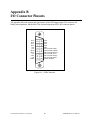
Figure B-1.
Figure B-2.
Figure B-3.
GPIB Connector ............................................................................................... B-1
NuBus Pin Assignments................................................................................... B-2
RTSI Bus Connector Pinout............................................................................. B-3
Tables
Table
Table
Table
Table
Table
Table
Table
Table
4-1.
4-2.
4-3.
4-4.
4-5.
4-6.
4-7.
4-8.
Macintosh Slot Addresses ................................................................................ 4-1
Register Map for the NB-DMA2800 Register Groups .................................... 4-2
Register Map for the GPIB Interface Register Group...................................... 4-3
Register Map for the 82380 Register Group .................................................... 4-4
Scan Circuitry for 82380 DMAC ..................................................................... 4-30
Legal Scan Modes–COMMAND<1..0> = 00 .................................................. 4-31
RTSI Switch Signals ........................................................................................ 4-34
82380 External Interrupt Sources..................................................................... 4-37
© National Instruments Corporation
ix
NB-DMA2800 User Manual
About This Manual
The NB-DMA2800 is a block-mode direct memory access (DMA) and GPIB interface board for
Macintosh NuBus computers. Other National Instruments NB Series boards are serviced by the
NB-DMA2800 so that acquired data is transferred directly to memory. The NB-DMA2800 also
contains a high-performance NuBus to GPIB interface, enabling data transfers between the
Macintosh and thousands of IEEE 488-compatible instruments.
Organization of This Manual
This manual describes the mechanical and electrical aspects of the NB-DMA2800 and contains
information concerning its operation and programming. The manual is divided into the following
chapters and appendixes:
Chapter 1, Introduction, describes the NB-DMA2800, lists what you need to get started, describes
the available software packages, lists optional equipment, and explains how to unpack the
NB-DMA2800.
Chapter 2, Installation, contains instructions for installing the NB-DMA2800 and connecting
cables.
Chapter 3, Theory of Operation, contains a functional overview of the NB-DMA2800 board and
explains the operation of each functional unit making up the NB-DMA2800.
Chapter 4, Programming, describes in detail the address and function of each of the
NB-DMA2800 control and status registers. This chapter also includes important information about
programming the NB-DMA2800.
Appendix A, Specifications, lists specifications of the NB-DMA2800.
Appendix B, I/O Connector Pinouts, shows the pinouts and signal names of the input/output (I/O)
connectors on the NB-DMA2800.
Appendix C, AMD Data Sheet, contains the manufacturer data sheet for the Am9513A/Am9513
System Timing Controller (Advanced Micro Devices, Inc.) integrated circuit. This circuit is used
on the NB-DMA2800.
Appendix D, Intel Data Sheet, contains the 82380 High Performance 32-Bit DMA Controller with
Integrated System Support Peripherals (Intel Corporation) data sheet. This device is used on the
NB-DMA2800.
Appendix E, Customer Communication, contains forms you can use to request help from National
Instruments or to comment on our products.
© National Instruments Corporation
xi
NB-DMA2800 User Manual
About This Manual
Glossary contains an alphabetical list of acronyms and abbreviations used in this manual.
Index alphabetically lists topics covered in this manual, including the page where the topic can be
found.
Conventions Used in This Manual
The following conventions are used in this manual:
italic
Italic text denotes emphasis, a cross reference, or an introduction to a key
concept.
monospace
Lowercase text in this font denotes text or characters that are to be literally
input from the keyboard, sections of code, programming examples, and
syntax examples. This font is also used for the proper names of disk drives,
paths, directories, programs, subprograms, subroutines, device names,
functions, variables, filenames, and extensions, and for statements and
comments taken from program code.
Macintosh
Macintosh refers to all Macintosh II and Macintosh Quadra computers
unless otherwise noted.
Related Documentation
The following documents contain information that may be helpful as you read this manual:
•
The Macintosh II or Quadra Owner's Manual, Getting Started manual, or Setting Up manual
•
NEC Electronics Inc. 1987 Data Book Microcomputer Products
Customer Communication
National Instruments wants to receive your comments on our products and manuals. We are
interested in the applications you develop with our products, and we want to help if you have
problems with them. To make it easy for you to contact us, this manual contains comment and
configuration forms for you to complete. These forms are in Appendix E, Customer
Communication.
NB-DMA2800 User Manual
xii
© National Instruments Corporation
Chapter 1
Introduction
This chapter describes the NB-DMA2800, lists the contents of your NB-DMA2800 kit, describes
the software packages available for the NB-DMA2800, lists the optional equipment for the
NB-DMA2800, and explains how to unpack the NB-DMA2800.
Overview
The NB-DMA2800 is a 32-bit DMA controller board for Macintosh NuBus computers with
NuBus (NB) block-mode master capability. It can be used for high-performance direct memory
access (DMA) service to other National Instruments NB Series boards. The NB-DMA2800 uses
Real-Time System Integration (RTSI) bus timing and interrupt support to integrate and optimize the
operations of the NB boards. Used alone or with other NB Series boards, the NB-DMA2800
offers a high-performance NuBus-to-GPIB interface, enabling data transfers between the
Macintosh and thousands of IEEE 488-compatible instruments. By itself, the NB-DMA2800
converts the Macintosh into one of the highest performance GPIB controllers available. The
NB DMA2800 transfers rates of data up to 1 Mbytes/sec, so it can be used with the fastest
IEEE 488 instruments in a wide variety of test, measurement, monitoring, and control applications.
The combination of the Macintosh, NB Series data acquisition boards, and the NB-DMA2800
introduces the next generation of high-performance personal computers for scientific and
engineering applications. High-speed DMA and the tightly integrated timing offered by the RTSI
bus are features unprecedented in personal computers. These hardware features merge with the
LabVIEW software system to create a new integrated instrumentation platform that makes rapid
development of high-performance test and measurement systems possible.
The NB-DMA2800 contains a high-performance GPIB interface. The National Instruments
Turbo488 custom-integrated circuit combined with the NEC µPD7210 offers complete IEEE 488
talker/listener/controller (TLC) capability; a first-in-first-out (FIFO) data buffer with enhanced
throughput including 1 Mbytes/sec GPIB reads, 700 kbytes/sec GPIB writes, and 320 kbytes/sec
GPIB commands; automatic hardware handling of last-byte operations; terminal count interrupt
synchronized with GPIB handshaking; GPIB command transferral under DMA control; and an
extra GPIB monitor and control port for board and bus level diagnostics.
The Intel 82380 DMA controller offers eight 32-bit DMA channels. The controller handles 8-bit,
16-bit, and 32-bit devices and automatically packs or unpacks data as required. The
NB-DMA2800 uses programmed logic array (PLA) technology to add multichannel scanning
features to the DMA interface. Using these features, other members of the NB Series can transfer
data to and from multiple buffers with no loss of efficiency. The NB-DMA2800 also offers DMA
flyby mode for input/output (I/O) boards that can be used for DMA flyby mode and NuBus block
mode for I/O and memory boards that can be used for NuBus block mode.
The NB-DMA2800 also includes an Am9513A five-channel System Timing Controller unit for
precise system timing with clock periods as low as 200 nsec. Three timer outputs can generate
DMA requests for precise timing of DMA transfer activity. Thus, the Am9513A offers the accurate
sample timing essential in a data acquisition system. The timer can also send signals to other NB
Series boards via RTSI bus lines.
© National Instruments Corporation
1-1
NB-DMA2800 User Manual
Introduction
Chapter 1
The NB-DMA2800 contains board-to-board trigger signal routing hardware. The RTSI switch is a
custom-integrated circuit developed by National Instruments that interfaces between the RTSI bus
and the System Timing Controller unit. The RTSI switch uses a crossbar switch to move any input
from the counter/timer to any of seven RTSI bus lines under software control. The System Timing
Controller can then communicate with other NB boards across the RTSI bus.
What You Need to Get Started
To set up and use your NB-DMA2800, you will need the following:
NB-DMA2800 board
NB-DMA2800 User Manual
NI-488.2 Macintosh OS software package, with manual and 2 disks
NI-488.2 Macintosh OS Software Reference Manual
Your NB-DMA2800 is shipped with NI-488.2 Macintosh OS. NI-488.2 is a comprehensive
package of programs and drivers that transform the Macintosh into a GPIB controller with
complete communications and bus management capability. The NI-488.2 package contains
language interfaces for Microsoft QuickBASIC, Macintosh Programmer's Workshop (MPW) C,
THINK C, HyperTalk, and Device Manager.
Optional Software
The NB-DMA2800 can be used with the NI-DAQ software for Macintosh. NI-DAQ has a library
of functions that can be called from your application programming environment. These functions
include routines for analog input (A/D conversion), buffered data acquisition (high-speed A/D
conversion), analog output (D/A conversion), waveform generation, digital I/O, counter/timer, SCXI,
RTSI, and self-calibration. NI-DAQ maintains a consistent software interface among its different
versions so you can switch between platforms with minimal modifications to your code. NI-DAQ
comes with language interfaces for MPW C, THINK C, Pascal, and Microsoft QuickBASIC. Any
language that uses Device Manager Toolbox calls can access NI-DAQ.
The NB-DMA2800 can also be used with LabVIEW 2, a software system that features interactive
graphics, a state-of-the-art user interface, and a powerful graphical programming language. The
LabVIEW 2 Data Acquisition VI Library, a series of VIs for using LabVIEW 2 with the Lab-LC
and other National Instruments boards, is included with LabVIEW 2. The LabVIEW 2 Data
Acquisition VI Library is functionally equivalent to the NI-DAQ software for Macintosh.
NB-DMA2800 User Manual
1-2
© National Instruments Corporation
Chapter 1
Introduction
Optional Equipment
National Instruments offers four different ribbon cables which can be used to connect the RTSI
connectors of multiple NB Series boards. The RTSI cables are 50-conductor cables with two, three,
four, or five 50-position connectors which mate with the RTSI connectors of the NB Series boards.
Unpacking
Your NB-DMA2800 board is shipped in an antistatic plastic bag to prevent electrostatic damage to
the board. Several components on the board may be damaged by electrostatic discharge. To avoid
such damage in handling the board, take the following precautions:
•
Touch the plastic bag to a metal part of your computer before removing the board from the bag.
•
Remove the board from the bag and inspect the board for loose components or any other sign
of damage. Notify National Instruments if the board appears damaged in any way. Do not
install a damaged board into your computer.
© National Instruments Corporation
1-3
NB-DMA2800 User Manual
Chapter 2
Installation
This chapter contains instructions for installing the NB-DMA2800 and connectingcables.
Hardware Installation
Within the manual shipped with your Macintosh computer, read the instructions for installing the
video card in the main unit. You can use these instructions as a universal board installation guide.
Read the entire installation procedure before installing the NB-DMA2800 into the Macintosh.
However, if you are using the NB-DMA2800 with other NB Series boards, keep in mind that all
NB Series boards should reside in adjacent slots because the Real-Time System Integration (RTSI)
bus cable must connect them together. Once installed, the operating system finds the board when
you turn on your computer.
Cable Connection
When using the NB-DMA2800 with other NB Series boards, connect the RTSI bus cable to each
board before closing the computer chassis. Plug the RTSI cable into each NB Series board. Hold
the end of the board when connecting the RTSI connector because there is no support under the
board. RTSI bus cables of various lengths are available from National Instruments. RTSI cable
connectors can be left free if there are more connectors than NB Series boards.
When using the NB-DMA2800 as a GPIB interface, install the GPIB extension connector before
attaching the GPIB cable to the NB-DMA2800. Push the extension connector into the
NB-DMA2800 connector and tighten the thumb screws on each side of the extension connector.
Finally, attach one end of the GPIB cable to the extension connector and tighten the thumb screws
on both sides of the GPIB connector. Figure 2-1 illustrates the connection.
© National Instruments Corporation
2-1
NB-DMA2800 User Manual
Installation
Chapter 2
NB-DMA2800 Board
GPIB Extension
Connector
GPIB Cable
Thumb Screws
Figure 2-1. GPIB Cable Connected to an NB-DMA2800
When the NB-DMA2800 installation is complete, the GPIB cable is ready to attach to a GPIB
device.
NB-DMA2800 User Manual
2-2
© National Instruments Corporation
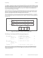
Chapter 3
Theory of Operation
This chapter gives a functional overview of the NB-DMA2800 board and explains the operation of
each functional unit making up the NB-DMA2800.
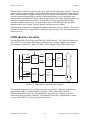
Functional Overview
The major components making up the NB-DMA2800 board are as follows:
•
NuBus slave interface circuitry
•
DMA and NuBus master interface circuitry
•
GPIB interface circuitry
•
Timer and RTSI bus interface circuitry
The internal data and control buses interconnect the components. The theory of operation of each
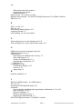
of these components is explained in the remainder of this chapter. Figure 3-1 is a block diagram of
the NB-DMA2800.
DMA
Controller
Timer Output
DRQ
Control
Data
Timer Gates
Address
32-Bit
Nubus
Master/
Slave
Interface
Trigger Bus
Interface
Timer Sources
DMA Requests
DMA
Requests
Scan
Circuitry
DMA
Acknowledges
RTSI Interrupts
RTSI
Interrupt
RTSI Bus
Clock
Prescaler
Block
Mode
Control
Address
Data
GPIB
NuBus
Am9513A Counter/Timer
Dedicated DMA Request
NMR
NMR
GPIB
Interrupt
Control
Turbo488
Read/Write
Port
16-Bits
GPIB
Transceivers
µPD7210
TLC
GPIB
Transceivers
Figure 3-1. NB-DMA2800 Block Diagram
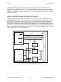
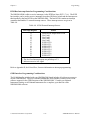
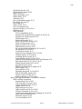
NuBus Slave Interface Circuitry
© National Instruments Corporation
3-1
NB-DMA2800 User Manual
Theory of Operation
Chapter 3
The NB-DMA2800 functions as a 32-bit NuBus slave board. The NuBus is a 32-bit address and
data bus with a 10-MHz clock. In addition, the NuBus contains interface signals for read and write
operations, and an interrupt line that can be driven by boards in NuBus slots. The components
making up the NB-DMA2800 NuBus slave interface circuitry are shown in Figure 3-2.
NB-DMA2800
Interrupt
Status
and
Control
CLK*
START*
ACK*
NuBu
TM*<1..0>
NuBus
Controller
NMR*
Transceiver
Control
DATA<31..0>
AD*<31..0>
ID*<3..0>
Read &
Write Signals
Slave
Interface
PALS
Configuration
EPROM
Decode
Enable
Internal
Data Bus
ADDR<31..0>
Internal
Address Bus
NuBus
Transceivers
Address
Decoders
Register
Selects
Figure 3-2. NuBus Slave Interface Circuitry Block Diagram
The NuBus interface circuitry consists of the Texas Instruments NuBus interface chip-set, address
decoder circuitry, EPROM, and NuBus non-master request (NMR) interrupt circuitry. This
interface circuitry generates the signals necessary to control and monitor the operation of the
NB-DMA2800 circuitry.
The NuBus interface chips on the NB-DMA2800 match NuBus address lines 27 through 24 to the
slot ID lines supplied by the slot that the board is plugged into. The board can then determine
when the slot that it occupies is being addressed. Each slot in the Macintosh has a unique slot
address. The address latches on the NB-DMA2800 latch all of the address lines from the NuBus.
Address lines 17 through 19 are decoded by the NB-DMA2800 address decoding circuitry to
generate selects for the onboard configuration ROM and other registers on the board. Address
lines 20 through 23 are left undecoded by the NB-DMA2800 board. The NB-DMA2800 can then
be compatible with both the 24-bit and 32-bit bus modes used by the Macintosh.
The NB-DMA2800 is a 32-bit slave and can use all 32 NuBus data lines. The NuBus interface
timing signals are decoded by the interface chips that generate the proper read and write signals for
the remaining NB-DMA2800 circuitry. The NuBus 10-MHz clock is used to synchronize the
NuBus interface timing circuitry.
The configuration ROM is an 8-kbyte EPROM that contains information related to the
NB-DMA2800 board. This ROM is read by the Macintosh Slot Manager upon system startup.
This configuration ROM is required by the NuBus so the Macintosh operating system and other
software can identify the board.
NB-DMA2800 User Manual
3-2
© National Instruments Corporation
Chapter 3
Theory of Operation
The NB-DMA2800 is able to cause interrupts in the Macintosh by driving the NMR interrupt line.
Note:
While the DMA controller (DMAC) controls the local bus, no other NuBus master
can access the NB-DMA2800. If the NB-DMA2800 is addressed as a NuBus slave
after the 82380 DMAC has been given the local bus on the board, the NB-DMA2800
issues a NuBus RETRY error. In general, this tells any board capable of becoming a
master in the Macintosh NuBus that the slave access to the NB-DMA2800 needs to be
tried again. However, the Macintosh generates a 68020 bus error when a NuBus
RETRY occurs. For this reason, a bus error handler must be installed in order to
operate the NB-DMA2800. This is not a problem if the National Instruments driver,
which comes with the NB-DMA2800, is installed. However, if you attempt to write
your own driver software for the NB-DMA2800, you must be aware of this situation
and have some sort of bus error handler installed. See Chapter 4, Programming, for
more information on installing and programming a bus error handler.
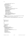
DMA and NuBus Master
The DMA circuit controls the flow of data between peripherals and memory. The NuBus interface
chips accept signals from the DMA controller and perform appropriate NuBus master operations,
such as arbitrations, reads, and writes. Figure 3-3 shows a block diagram of the DMA and NuBus
master logic.
GPIB DMA Acknowledge
HOLD
NuBus
Request
HLDA
W/R*
Intel
82380
DMAC
BE*<3..0>
RQST*
Master
Interface
PALS
Status and
Control
NuBus
Controller
START*
ACK*
NuBus
ADS*
ARB*<3..0>
TM*<1..0>
READY*
Transceiver
Control
ADDR<31..24>
ID*<3..0>
AD*<31..0>
ADDR<31..0>
NuBus
Transceivers
DATA<31..0>
Figure 3-3. DMA and NuBus Master Circuitry Block Diagram
© National Instruments Corporation
3-3
NB-DMA2800 User Manual
Theory of Operation
Chapter 3
When the DMA controller is ready to read or write data, it asserts hold request (HOLD). Then, the
interface circuitry grants the DMA controller the local bus by asserting hold acknowledge (HLDA)
and the DMA controller, sensing the assertion of HLDA, begins its bus operations. If the interface
circuitry determines that the DMA controller is addressing memory or I/O in an address space
other than that of the NB-DMA2800, the interface chips perform the NuBus arbitration sequence in
accordance with the NuBus specification. If the interface circuitry determines that the DMA
controller is addressing memory or I/O in the address space of the NB-DMA2800, the DMA
transaction takes place with the Turbo488 instead of going out over the NuBus.
When the DMA controller has completed all pending transactions, it releases HOLD. The interface
circuitry senses the release, negates HLDA, and releases the local bus to any other master that may
want access to it.
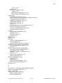
GPIB Interface Circuitry
The NB-DMA2800 offers a high-speed IEEE 488 (GPIB) interface. The Turbo488 enhances the
NEC µPD7210 for a complete talker/listener/controller (TLC) interface capable of data transfer
rates as high as 1 Mbytes/sec. Figure 3-4 shows a block diagram of the GPIB interface logic.
GPIB DMA Acknowledge
DATA
Chip Select
Turbo488
GPIB
Bus
Transceivers
DATA
CONTROL
CONTROL
NEC
µPD7210
Chip Select
Bus
Transceivers
Diagnostic
Register
Figure 3-4. GPIB Interface Circuitry Block Diagram
The Turbo488 responds to 8-bit or 16-bit read and write operations. When the proper address
appears on the NuBus, or when the DMAC generates a DMA acknowledge inside the
NB-DMA2800 address space, the Turbo488 interface logic generates a chip select or DMA
acknowledge that activates the Turbo488. The Turbo488, if necessary, performs data or control
accesses to the µPD7210 to carry out the desired function.
NB-DMA2800 User Manual
3-4
© National Instruments Corporation
Chapter 3
Theory of Operation
The NB-DMA2800 has specialized hardware for monitoring and controlling GPIB activity
independent of the µPD7210 interface. The complete GPIB status can be read using this circuitry,
and any line can be driven at any time. This is used to synchronize GPIB activity and to simplify
software. Comprehensive hardware diagnostics can also be performed without the use of a special
loop-back connector.
Timer and RTSI Bus Interface Circuitry
DMA requests and interrupts from other NB Series boards can be received by the 82380 via the
NB-DMA2800 bus interface. The Am9513A receives its master clock from the TOUT1* output of
the Intel 82380. Each of the Am9513A outputs is tied to one of the RTSI switches so that the
NB-DMA2800 can distribute timing signals across the system. Also, the Am9513A source and
gate inputs are connected to a RTSI switch so the NB-DMA2800 can use timing signals generated
elsewhere in the system. Three of the Am9513A outputs can be used to generate constant DMA
requests on the RTSI bus DMA request lines. Figure 3-5 shows a block diagram of the Am9513A
Timer/Counter Unit, 82380 and RTSI switches.
82380
IRQX
EDACKX
EOP
DMARQX
Interrupt Request
/
EDACKX
/
EOP
DMA Request
8
3
/8
/3
TOUTX
RTSI Bus
OpenCollector
Buffers
AM9513A
OUTPUTS
RTSI
Switch 2
/
7
GATES
RTSI
Switch 1
FOUT
SOURCES
Figure 3-5. Am9513A Timer and RTSI Interface
© National Instruments Corporation
3-5
NB-DMA2800 User Manual
Chapter 4
Programming
This chapter describes in detail the address and function of each of the NB-DMA2800 control and
status registers. This chapter also includes important information about programming the
NB-DMA2800.
Register Access
The Macintosh uses memory mapping to access boards in the system. The following sections
discuss how to access the various registers on the NB-DMA2800.
Slot Address Space
Each slot in the Macintosh is allocated a block of Macintosh memory addresses known as the slot
address space. All I/O boards plugged into Macintosh slots are therefore memory mapped. When
an I/O board is plugged into a given slot, its registers can be accessed within that slot address space.
The block of memory addresses allocated to each slot depends on the slot number and whether the
Macintosh memory manager is in 24-bit or 32-bit addressing mode. The slots are labeled 9
through E next to the slot connectors inside the Macintosh II, IIx, and IIfx; 9 through B inside the
Macintosh IIcx; C through E inside the Macintosh IIci; D through E inside the
Quadra 700; and A through E inside the Quadra 900. The Macintosh IIsi has a single slot
labeled 9. Table 4-1 shows the slot address space for each slot, both for 24-bit compatibility mode
and for 32-bit mode.
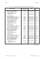
Table 4-1. Macintosh Slot Addresses
Slot Number
9
A
B
C
D
E
Base Address for 24-bit
Compatibility Mode
0090 0000
00A0 0000
00B0 0000
00C0 0000
00D0 0000
00E0 0000
Base Address
for 32-bit mode
F900 0000
FA00 0000
FB00 0000
FC00 0000
FD00 0000
FE00 0000
The register maps for the NB-DMA2800 are given in Table 4-2, Table 4-3, and Table 4-4. These
tables list the register name, the register address offset from the slot base address, the type of the
register (read only, write only, or read and write), and the size of the register in bits.
© National Instruments Corporation
4-1
NB-DMA2800 User Manual
Programming
Chapter 4
Register Maps
Each register address in Table 4-2, Table 4-3, and Table 4-4 is the offset address from the slot
starting address. To calculate the absolute address of a register, add the slot base address given in
Table 4-1 to the register offset given in Table 4-2, Table 4-3, or Table 4-4. For example, if the NBDMA2800 is plugged into slot B and the Macintosh is operating in 24-bit compatibility mode, the
GPIB Monitor register is at location (B0 0000 + 2 0000); that is, address B2 0000 (hex).
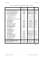
Table 4-2. Register Map for the NB-DMA2800 Register Groups
Register Name
Offset Address
(Hex)
Type
Size
Configuration Register Group
Board Control Register
Scan Circuitry Bypass Register
EOP Interrupt Enable Register
NuBus Block Mode Enable Register
NuBus Flyby Enable Register
NuBus MLock Enable Register
4 0000
4 0007
4 000B
4 000F
4 0013
4 0017
Write-only
Write-only
Write-only
Write-only
Write-only
Write-only
32-bit
8-bit
8-bit
8-bit
8-bit
8-bit
RTSI Switch Register Group
RTSI Switch 1 Shift Register
RTSI Switch 2 Shift Register
RTSI Switch 1 Strobe Register
RTSI Switch 2 Strobe Register
A 0000
C 0000
A 0004
C 0004
Write-only
Write-only
Write-only
Write-only
8-bit
8-bit
8-bit
8-bit
6 0000
6 0004
Read-only
Read-and-write
Write-only
16-bit
16-bit
16-bit
Am9513A System Timing Controller
Register Group
Data Port Register
Command Port Register
Status Register6 0004
Refer to Appendix C, AMD Data Sheet, for information about the Am9513A Register Group.
NB-DMA2800 User Manual
4-2
© National Instruments Corporation
Chapter 4
Programming
Table 4-3. Register Map for the GPIB Interface Register Group
Register Name
Offset Address
(Hex)
Type
Size
0 0001
0 0001
0 0005
0 0005
0 0009
0 0009
0 000D
0 0011
0 0011
0 0015
0 0015
0 0019
0 0019
0 001D
0 001D
Read-only
Write-only
Read-only
Write-only
Read-only
Write-only
Read-and-write
Read-only
Write-only
Read-only
Write-only
Read-only
Write-only
Read-only
Write-only
8-bit
8-bit
8-bit
8-bit
8-bit
8-bit
8-bit
8-bit
8-bit
8-bit
8-bit
8-bit
8-bit
8-bit
8-bit
0 0021
0 0021
0 0025
0 0029
0 002D
Read-and-write
0 0035
0 0035
0 0039
0 0039
Read-and-write
Read-only
Write-only
Read-and-write
Read-and-write
Read-and-write
16-bit
Read-only
Write-only
Read-only
Write-only
8-bit
8-bit
8-bit
8-bit
8-bit
8-bit
2 0000
Read-and-write
GPIB Interface Register Group
µPD7210 Register Group
Data In Register
Command/Data Out Register
Interrupt Status 1 Register
Interrupt Mask 1 Register
Interrupt Status 2 Register
Interrupt Mask 2 Register
Serial Poll Status Register
Address Status Register
Address Mode Register
Command Pass-Through Register
Auxiliary Mode Register
Address Register 0
Address Register 0/1
Address Register 1
End of String Register
Turbo488 Register Group
Status 1 Register
Configuration Register
Interrupt Mask 3 Register
Count Low Register
Count High Register
FIFO Memory0 0030
Interrupt Status 3 Register
Carry Cycle Register
Status Register 2
Command Register
Timer Register0 003D
GPIB Monitor Register
© National Instruments Corporation
4-3
8-bit
8-bit
8-bit
8-bit
16-bit
NB-DMA2800 User Manual
Programming
Chapter 4
Table 4-4. Register Map for the 82380 Register Group
Register Name
Offset Address
(Hex)
Type
Size
8 0000
9 0085
8 0010
8 0001
8 0011
Read-and-write
Read-and-write
Read-and-write
Read-and-write
Read-and-write
8-bit
8-bit
8-bit
8-bit
8-bit
8 0090
Read-and-write
8-bit
8 0091
Read-and-write
8-bit
9 0000
9 0081
9 0010
9 0001
9 0011
Read-and-write
Read-and-write
Read-and-write
Read-and-write
Read-and-write
8-bit
8-bit
8-bit
8-bit
8-bit
9 0090
Read-and-write
8-bit
9 0091
Read-and-write
8-bit
8 0004
8 0081
8 0014
8 0005
8 0015
Read-and-write
Read-and-write
Read-and-write
Read-and-write
Read-and-write
8-bit
8-bit
8-bit
8-bit
8-bit
8 0094
Read-and-write
8-bit
8 0095
Read-and-write
8-bit
9 0004
9 0080
9 0014
9 0005
Read-and-write
Read-and-write
Read-and-write
Read-and-write
8-bit
8-bit
8-bit
8-bit
82380 Register Group
Channel 0 Registers
Target Address Register (Bytes <0..1>)
Target Address Register (Byte 2)
Target Address Register (Byte 3)
Byte Count Register (Bytes <0..1>
Byte Count Register (Byte 2)
Requester Address Register
(Bytes <0..1>)
Requester Address Register
(Bytes <2..3>)
Channel 1 Registers
Target Address Register (Bytes <0..1>)
Target Address Register (Byte 2)
Target Address Register (Byte 3)
Byte Count Register (Bytes <0..1>
Byte Count Register (Byte 2)
Requester Address Register
(Bytes <0..1>)
Requester Address Register
(Bytes <2..3>)
Channel 2 Registers
Target Address Register (Bytes <0..1>)
Target Address Register (Byte 2)
Target Address Register (Byte 3)
Byte Count Register (Bytes <0..1>
Byte Count Register (Byte 2)
Requester Address Register
(Bytes <0..1>)
Requester Address Register
(Bytes <2..3>)
Channel 3 Registers
Target Address Register (Bytes <0..1>)
Target Address Register (Byte 2)
Target Address Register (Byte 3)
Byte Count Register (Bytes <0..1>
(continues)
NB-DMA2800 User Manual
4-4
© National Instruments Corporation
Chapter 4
Programming
Table 4-4. Register Map for the 82380 Register Group (Continued)
Register Name
Offset Address
(Hex)
Type
Size
9 0015
Read-and-write
8-bit
9 0094
Read-and-write
8-bit
9 0095
Read-and-write
8-bit
8 00C0
9 008D
8 00D0
8 00C1
8 00D1
Read-and-write
Read-and-write
Read-and-write
Read-and-write
Read-and-write
8-bit
8-bit
8-bit
8-bit
8-bit
8 0098
Read-and-write
8-bit
8 0099
Read-and-write
8-bit
9 00C0
9 0089
9 00D0
9 00C1
9 00D1
Read-and-write
Read-and-write
Read-and-write
Read-and-write
Read-and-write
8-bit
8-bit
8-bit
8-bit
8-bit
9 0098
Read-and-write
8-bit
9 0099
Read-and-write
8-bit
8 00C4
8 0089
8 00D4
8 00C5
8 00D5
Read-and-write
Read-and-write
Read-and-write
Read-and-write
Read-and-write
8-bit
8-bit
8-bit
8-bit
8-bit
8 009C
Read-and-write
8-bit
8 009D
Read-and-write
8-bit
Byte Count Register (Byte 2)
Requester Address Register
(Bytes <0..1>)
Requester Address Register
(Bytes <2..3>)
Channel 4 Registers
Target Address Register (Bytes <0..1>)
Target Address Register (Byte 2)
Target Address Register (Byte 3)
Byte Count Register (Bytes <0..1>
Byte Count Register (Byte 2)
Requester Address Register
(Bytes <0..1>)
Requester Address Register
(Bytes <2..3>)
Channel 5 Registers
Target Address Register (Bytes <0..1>)
Target Address Register (Byte 2)
Target Address Register (Byte 3)
Byte Count Register (Bytes <0..1>
Byte Count Register (Byte 2)
Requester Address Register
(Bytes <0..1>)
Requester Address Register
(Bytes <2..3>)
Channel 6 Registers
Target Address Register (Bytes <0..1>)
Target Address Register (Byte 2)
Target Address Register (Byte 3)
Byte Count Register (Bytes <0..1>
Byte Count Register (Byte 2)
Requester Address Register
(Bytes <0..1>)
Requester Address Register
(Bytes <2..3>)
(continues)
© National Instruments Corporation
4-5
NB-DMA2800 User Manual
Programming
Chapter 4
Table 4-4. Register Map for the 82380 Register Group (Continued)
Register Name
Offset Address
(Hex)
Type
Size
9 00C4
9 0088
9 00D4
9 00C5
9 00D5
Read-and-write
Read-and-write
Read-and-write
Read-and-write
Read-and-write
8-bit
8-bit
8-bit
8-bit
8-bit
9 009C
Read-and-write
8-bit
9 009D
Read-and-write
8-bit
8 0008
9 0018
9 0009
9 0019
8 0009
9 0008
9 000D
Read-only
8 0018
8 0019
Write-only
Write-only
Write-only
Write-only
Read-and-write
Write-only
Read-and-write
8-bit
Write-only
Read-and-write
8-bit
8-bit
8-bit
8-bit
8-bit
8-bit
8-bit
8 00C8
9 00D8
9 00C9
9 00D9
8 00C9
9 00C8
9 00CD
Read-only
8 00D8
8 00D9
Read-and-write
Read-and-write
Read-and-write
Read-and-write
Read-and-write
Write-only
Read-and-write
8-bit
Write-only
Read-and-write
8-bit
8-bit
8-bit
8-bit
8-bit
8-bit
8-bit
8 000C
8 000D
Write-only
Write-only
8-bit
8-bit
Channel 7 Registers
Target Address Register (Bytes <0..1>)
Target Address Register (Byte 2)
Target Address Register (Byte 3)
Byte Count Register (Bytes <0..1>
Byte Count Register (Byte 2)
Requester Address Register
(Bytes <0..1>)
Requester Address Register
(Bytes <2..3>)
Group 1 Registers (Channels 0 through 3)
Command Register 1
Command Register 2
Mode Register 1
Mode Register 2
Software Request Register
Mask Set/Reset Register
Mask Read/Write Register
Status Register8 0008
Bus Word Size Register
Chaining Register
Group 2 Registers
(Channels 4 through 7)
Command Register 1
Command Register 2
Mode Register 1
Mode Register 2
Software Request Register
Mask Set/Reset Register
Mask Read/Write Register
Status Register8 00C8
Bus Word Size Register
Chaining Register
Software Command Register Group
Clear Byte Pointer Flip-Flop Register
Master Clear Register
8-bit
8-bit
8-bit
8-bit
(continues)
NB-DMA2800 User Manual
4-6
© National Instruments Corporation
Chapter 4
Programming
Table 4-4. Register Map for the 82380 Register Group (Continued)
Register Name
Offset Address
(Hex)
Type
Size
9 000C
Write-only
8-bit
9 00CC
9 001C
Write-only
Write-only
8-bit
8-bit
8 0040
8 0041
9 0040
9 0041
8 0044
9 0045
8 0061
Read-and-write
Read-and-write
Read-and-write
Write-only
Read-and-write
Write-only
Write-only
8-bit
8-bit
8-bit
8-bit
8-bit
8-bit
8-bit
Clear Mask Register
(Channels 0 through 3)
Clear Mask Register
(Channels 4 through 7)
Clear TC Interrupt Request Register
Programmable Interval Timer Register
Group
Counter 0 Register
Counter 1 Register
Counter 2 Register
Control Word Register 1
Counter 3 Register
Control Word Register 2
Internal Control Port
Refer to Appendix D, Intel Data Sheet, for information about the 82380 Register Group.
Note:
Not all the Intel 82380 registers are listed in Table 4-4. To find the proper offset for
an 82380 register, use the following procedure: if bit 1 (next to the least significant
bit) of the register offset is 1, set bit 1 to 0 and set bit 16 to 1. Add the result to 8 0000
(hex), the offset of the 82380 group.
Example: If the register offset given in Appendix D, Intel Data Sheet, is 0D, then the
offset becomes 8 000D because bit 1 is 0 and the result is added to 8 0000. However, if
the register offset of 0F, then the offset becomes 9 000D, because bit 1 is 1. Thus, bit 1 is
changed to 0 and bit 16 is changed to 1.
Register Word Sizes
The Macintosh accepts three different memory word sizes for memory read and write operations:
byte (8-bit), half-word (16-bit), and word (32-bit). Table 4-2, Table 4-3, and Table 4-4 show the
word sizes of the NB-DMA2800 registers. For example, a 16-bit read is required to access the
first-in-first-out (FIFO) memory on the Turbo488, whereas an 8-bit write operation is required to
program the RTSI Strobe 1 Register. All 82380 transactions are byte transactions.
Note:
Register sizes and access types given in this chapter take precedence over those
specified in the appendixes.
© National Instruments Corporation
4-7
NB-DMA2800 User Manual
Programming
Chapter 4
Register Description
Table 4-2, Table 4-3, and Table 4-4 divide the NB-DMA2800 registers into different register
groups. A bit description of each of the registers making up these groups is given later in this
chapter or in the related appendix (Appendix C, AMD Data Sheet, or Appendix D, Intel Data
Sheet).
The Configuration Register Group controls the overall operation of the NB-DMA2800 hardware.
The RTSI Switch Register Group controls routing of the system timing and control signals over the
RTSI bus trigger lines. The Am9513A System Timing Controller Register Group controls the
programmable timers contained within the Am9513A IC. The GPIB Interface Register Group,
including the Turbo488 and the µPD7210 Registers, controls the sophisticated GPIB interface used
by the NB-DMA2800. The GPIB Monitor Register allows control and monitoring of the GPIB
independent of the GPIB Interface Register Group and is used for hardware diagnostics. The
82380 Register Group controls the DMA controller (DMAC), interrupt controller, and
programmable interval timer hardware contained within the 82380 integrated circuit (IC).
Register Description Format
The remainder of this register description section discusses most of the NB-DMA2800 registers in
the order shown in Table 4-2, Table 4-3, and Table 4-4. Each register group is introduced, followed
by a detailed bit description of each register. Individual register descriptions give the address–
always in hexadecimal, type, data size, and bit map of the register, followed by a description of each
bit.
The register bit map shows a diagram of the register with the most significant bit (bit 31 for a
32-bit register, bit 15 for a 16-bit register, or bit 7 for an 8-bit register) shown on the left, and the
least significant bit (bit 0) shown on the right. A square is used to represent each bit. Each bit is
labeled with a name inside its square. An asterisk (*) after the bit name indicates that the bit is
inverted (negative logic).
In many of the registers, several bits are labeled with an x, indicating don't care bits. When a
register is read, these bits may appear set or cleared but should be ignored because they have no
significance. When a register is written to, setting or clearing these bit locations has no effect on
the NB-DMA2800 hardware.
The bit map field for some write-only addresses state not applicable, no bits used. Writing to these
addresses generates a strobe in the NB-DMA2800. These strobes are used to cause some onboard
event to occur. For example, writing to the RTSI Switch Strobe Register loads the contents of the
RTSI Switch Shift Register into the RTSI Switch Control Register. The data written to the Strobe
Register is ignored.
NB-DMA2800 User Manual
4-8
© National Instruments Corporation
Chapter 4
Programming
Configuration Register Group
The six registers making up the Configuration Register Group are used for general control of the
NB-DMA2800 hardware. The Configuration Register Group contains bits that control operation
of several different pieces of the NB-DMA2800 hardware.
Bit descriptions of the six registers making up the Configuration Register Group are given on the
following pages.
© National Instruments Corporation
4-9
NB-DMA2800 User Manual
Programming
Chapter 4
Board Control Register
The Board Control Register controls several NB-DMA2800 functions. Because it is accessed by
32-bit writes only, a software copy of its current state should be maintained. The Board Control
Register is cleared at system startup.
Address:
4 0000
Type:
Write-only
Word Size:
32-bit
Bit Map:
31
30
29
NMRIE
RTSIE
TDMA6
23
22
21
MODEB
LIMB2
LIMB1
15
14
13
DMANMR*
X
X
28
TDMA5
20
27
26
25
24
TDMA0
DRQ4
CMD1
CMD0
19
18
17
16
MODEA
LIMA2
LIMA1
LIMA0
12
11
10
9
X
X
X
X
LIMB0
8
X
7
6
5
4
3
2
1
0
X
X
X
X
X
X
X
X
Bit
Name
Description
31
NMRIE
Non-Master Request Interrupt Enable. Setting this bit allows
the GPIB interface circuitry to interrupt the Macintosh II's
68020 microprocessor by asserting the NuBus NMR*
signal.
30
RTSIE
RTSI Interrupt Enable. Setting this bit allows the GPIB
interface circuitry to send an interrupt across one of the eight
RTSI bus interrupts, INT*<7..0>. The interrupt line used is
determined by the lower three bits of the NB-DMA2800 slot
number. For example, if the NB-DMA2800 is in slot B, then
the GPIB interrupt would use INT*3, because the lower
three bits of hexadecimal slot number B equals 3.
29
TDMA6
Timer DMA request enable. Setting this bit connects the
Am9513A Out4 signal to the DMARQ*6 line, allowing
generation of periodic DMA requests.
NB-DMA2800 User Manual
4-10
© National Instruments Corporation
Chapter 4
Programming
Bit
Name
Description (continued)
28
TDMA5
Timer DMA request enable. Setting this bit connects the
Am9513A Out2 signal to the DMARQ*5 line, allowing
generation of periodic DMA requests.
27
TDMA0
Timer DMA request enable. Setting this bit connects the
Am9513A Out3 signal to the DMARQ*0 line, allowing
generation of periodic DMA requests.
26
DRQ4
Setting this bit connects DMARQ*0 to DMARQ*4,
allowing 8-channel and 6-channel scanning modes. If this
bit is clear, each scanning circuit operates independently and
DMARQ*4 is driven by the GPIB interface DMA request
line.
25
CMD1
Command high. This bit controls the scanning circuitry.
24
CMD0
Command low. This bit controls the scanning circuitry.
23
MODEB
This bit controls the mode of Scan Circuit B.
22-20
LIMB<2..0>
Limit parameters for Scan Circuit B.
19
MODEA
This bit controls the mode of Scan Circuit A.
18-16
LIMA<2..0>
Limit parameters for Scan Circuit A.
15
DMANMR*
Clearing this bit allows the 82380 INT pin to assert the
NuBus NMR* signal.
14-0
X
Don't care bits.
© National Instruments Corporation
4-11
NB-DMA2800 User Manual
Programming
Chapter 4
Scan Circuitry Bypass Register
Setting bit n in this register connects RTSI line DMARQ*n directly to 82380 DMA Request Input
DREQn.
Address:
4 0007
Type:
Write-only
Word Size:
8-bit
Bit Map:
7
6
5
SCB7
SCB6
SCB5
4
SCB4
3
2
1
0
SCB3
SCB2
SCB1
SCB0
Bit
Name
Description
7-0
SCB<7..0>
Scan Circuitry Bypass. Setting this bit will bypass the scan
circuitry for DMA Channels 7 through 0, respectively, and
connect the RTSI line DMARQ*7 through DMARQ*0
directly to the 82380 DMA request input DREQ7 through
DREQ0.
NB-DMA2800 User Manual
4-12
© National Instruments Corporation
Chapter 4
Programming
EOP Interrupt Enable Register
Clearing bit n in this register enables an end of process (EOP) for DMA Channel n to trigger
interrupt request 11 on the 82380.
Address:
4 000B
Type:
Write-only
Word Size:
8-bit
Bit Map:
7
6
5
EIE*7
EIE*6
EIE*5
4
EIE*4
3
2
1
0
EIE*3
EIE*2
EIE*1
EIE*0
Bit
Name
Description
7-0
EIE*<7..0>
EOP Interrupt Enable. Clearing this bit enables an EOP for
DMA Channels 7 through 0, respectively, to trigger interrupt
request 11 on the 82380.
Note:
After power on, all bits are clear; therefore, all EOP interrupts are enabled.
© National Instruments Corporation
4-13
NB-DMA2800 User Manual
Programming
Chapter 4
NuBus Block Mode Enable Register
Setting bit n in this register enables NuBus block mode for DMA Channel n. 82380 DMA
Channel n should be programmed for DMA flyby.
Address:
4 000F
Type:
Write-only
Word Size:
8-bit
Bit Map:
7
6
5
NBE7
NBE6
NBE5
4
NBE4
3
2
1
0
NBE3
NBE2
NBE1
NBE0
Bit
Name
Description
7-0
NBE<7..0>
NuBus Block Mode Enable. Setting this bit enables NuBus
block mode for DMA Channels 7 through 0, respectively.
82380 DMA Channels 7 through 0 should be programmed
for DMA flyby.
NB-DMA2800 User Manual
4-14
© National Instruments Corporation
Chapter 4
Programming
NuBus Flyby Enable Register
Setting bit n in this register enables NuBus flyby for DMA Channel n. 82380 DMA Channel n
should be programmed for DMA flyby.
Address:
4 0013
Type:
Write-only
Word Size:
8-bit
Bit Map:
7
6
5
NFE7
NFE6
NFE5
4
NFE4
3
2
1
0
NFE3
NFE2
NFE1
NFE0
Bit
Name
Description
7-0
NFE<7..0>
NuBus Flyby Enable. Setting this bit enables NuBus flyby
for DMA Channels 7 through 0, respectively.
© National Instruments Corporation
4-15
NB-DMA2800 User Manual
Programming
Chapter 4
NuBus MLock Enable Register
Setting bit n in this register enables NuBus master resource lock request for DMA Channel n.
82380 DMA Channel n should be programmed for DMA flyby.
Address:
4 0017
Type:
Write-only
Word Size:
8-bit
Bit Map:
7
6
5
NMLE7
NMLE6
NMLE5
4
X
3
2
1
0
NMLE3
NMLE2
NMLE1
NMLE0
Bit
Name
Description
7-5, 3-0
NMLE<7..0>
NuBus MLock Enable. Setting this bit enables NuBus
master resource lock request for DMA Channels 7 through
0, respectively. 82380 DMA Channels 7 through 0 should
be programmed for DMA flyby.
4
X
Don't care bit.
NB-DMA2800 User Manual
4-16
© National Instruments Corporation
Chapter 4
Programming
RTSI Switch Register Group
The four registers making up the RTSI Switch Register Group are used to program the
NB-DMA2800 RTSI switch to route the signals on the RTSI bus trigger lines to and from several
NB-DMA2800 signal lines. The RTSI switch is programmed by shifting a 56-bit routing pattern
into the RTSI switch and then loading the internal RTSI Switch Control Register. The routing
pattern is shifted into the RTSI switch by writing one bit at a time to the RTSI Switch Shift
Register. The RTSI Switch Control Register is then loaded by writing to the RTSI Switch Strobe
Register.
Bit descriptions for the registers making up the RTSI Switch Register Group are given on the
following pages.
© National Instruments Corporation
4-17
NB-DMA2800 User Manual
Programming
Chapter 4
RTSI Switch Shift Registers
The RTSI Switch Shift Registers are written to in order to load the RTSI switch internal 56-bit Control
Register with routing information for switching signals to and from the RTSI bus trigger lines. The
RTSI Switch Shift Registers are 1-bit registers and must be written to 56 times in order to shift the 56
bits into the internal registers.
Address:
A 0000
C 0000
Type:
Write-only
Word Size:
8-bit
RTSI Switch 1
RTSI Switch 2
Bit Map:
7
6
5
4
3
2
1
0
X
X
X
X
X
X
X
RSI
Bit
Name
Description
7-1
X
Don't care bits
0
RSI
RTSI Switch Serial Input. This bit is the serial input to the RTSI
switch. Each time the RTSI Shift Register is written to, the value
of this bit is shifted into the RTSI switch.
NB-DMA2800 User Manual
4-18
© National Instruments Corporation
Chapter 4
Programming
RTSI Switch Strobe Registers
The RTSI Switch Strobe Registers are written to in order to load the contents of the RTSI Switch
Shift Register into the RTSI Switch Control Register, thereby updating the RTSI switch routing
pattern. The RTSI Switch Strobe Registers are written to after shifting the 56-bit routing pattern
into the RTSI Switch Shift Registers. The data written to the Strobe Register is ignored.
Address:
A 0004
C 0004
RTSI Switch 1
RTSI Switch 2
Type:
Write-only
Word Size:
8-bit
Bit Map:
Not applicable, no bits are used
© National Instruments Corporation
4-19
NB-DMA2800 User Manual
Programming
Chapter 4
GPIB Register Group
The GPIB Interface Register Group contains the sophisticated GPIB interface made up of the
National Instruments Turbo488 and NEC µPD7210. National Instruments offers extensive
software support for the GPIB functions of the NB-DMA2800, including the NI-488 handler that
is included with the NB-DMA2800 and optional source code software support. The GPIB
Interface Register Group also includes the GPIB Monitor Register that is connected directly to the
GPIB, allowing control and monitoring of the GPIB independent of the Turbo488 and the
µPD7210. This register is used for hardware diagnostics.
NB-DMA2800 User Manual
4-20
© National Instruments Corporation
Chapter 4
Programming
GPIB Monitor Register
The bits of this register are connected directly to the GPIB lines.
Address:
2 0000
Type:
Read-and-write
Word Size:
16-bit
Bit Map:
15
14
13
DIO*8
DIO*7
DIO*6
7
6
5
EOI*
ATN*
SRQ*
12
DIO*5
4
REN*
11
10
9
8
DIO*4
DIO*3
DIO*2
DIO*1
3
2
1
0
IFC*
NRFD*
NDAC*
DAV*
Bit
Name
Description
15-8
DIO*<8..1>
Data Input/Output. 8-bit bidirectional bus for the transfer of
a message on the GPIB.
7
EOI*
End or Identify. Control line used to indicate the end of a
multiple byte transfer sequence or to execute a parallel
polling in conjunction with ATN.
6
ATN*
Attention. Control line which indicates whether the data on
DIO lines is an interface message or a device-dependent
message.
5
SRQ*
Service Request. Control line used to request the controller
for service.
4
REN*
Remote Enable. Control line used to select remote or local
control of the devices.
3
IFC*
Interface Clear. Control line used for clearing the interface
functions.
2
NRFD*
Ready for Data. Handshake line indicating that the device is
ready for data.
1
NDAC*
Data Accepted. Handshake line indicating the completion of
message reception.
0
DAV*
Data Valid. Handshake line indicating that the data on DIO
lines is valid.
© National Instruments Corporation
4-21
NB-DMA2800 User Manual
Programming
Chapter 4
The Configuration EPROM
The Configuration EPROM is an onboard read-only memory that contains information required by
the Macintosh operating system.
The Configuration EPROM on the NB-DMA2800 contains information about the NuBus interface
and is required by the Macintosh. The Macintosh System Slot Manager reads the Configuration
EPROM during system startup.
The Configuration EPROM is mapped to address offset E 0000 through F FFFC. The EPROM is
1 byte wide and 8 kbytes in length. Each byte of the EPROM is mapped to every fourth address
location on the NB-DMA2800: the first byte is read from location (slot address + E 0000), the
second byte is read from location (slot address + E 0004), and so on. With this mapping, there are
four aliases of each EPROM location. Thus, E 0000 through E 7FFC equals E 8000 through E
FFFC equals F 0000 through F 7FFC equals F 8000 through F FFFC.
Programming Considerations
The remainder of this chapter contains programming instructions for operating the circuitry on the
NB-DMA2800 board. Programming the NB-DMA2800 involves writing to and reading from the
various registers on the board. The programming instructions list the sequence of steps to take.
The instructions are language independent; that is, they instruct you to write a value to a given
register, to set or clear a bit in a given register, or to detect whether a given bit is set or cleared
without presenting the actual code.
Register Programming Considerations
Registers in the Macintosh are memory mapped; that is, to write to a register, you must store a value
in the appropriate memory location. To read a register, you must read the appropriate memory
location. Only memory location reads and writes can be performed on the
NB-DMA2800 registers. Mathematical or logical operations cannot be applied directly to the
NB-DMA2800 registers. Attempting to do so results in unpredictable program behavior.
Several write-only registers on the NB-DMA2800 contain bits that control independent pieces of
the onboard circuitry. In the instructions for setting or clearing bits, specific register bits must be
set or cleared without changing the current state of the remaining bits in the register. However,
writing to these registers affects all register bits simultaneously. You cannot read these registers to
determine which bits have been set or cleared in the past; therefore, you need to maintain a software
copy of the write-only registers. This software copy can then be read to determine the status of the
write-only registers. To change the state of a single bit without disturbing the remaining bits, set or
clear the bit in the software copy and write the software copy to the register.
NB-DMA2800 User Manual
4-22
© National Instruments Corporation
Chapter 4
Programming
Initializing the NB-DMA2800 Board
Use the following steps to initialize the NB-DMA2800 DMA circuitry:
1. Write 0300 8000 to the Board Control Register (32-bit write) to reset the scanning circuitry.
Follow with a write of 0000 8000 to the Board Control Register (32-bit write) to disable DMA
requests from the Am9513A.
2. Write 00 to the 82380 Master Clear Register (offset = 8 000D) to reset the 82380 DMA
controller (8-bit write).
3. Write 0F (hex) to the 82380 Mask Read/Write Registers to disable all DMA channels.
Bus Error Handler Installation and Programming Considerations
Because the NB-DMA2800 occasionally issues a NuBus RETRY during slave operations (see
Chapter 3, Theory of Operation), you must have a bus error handler installed. This bus error
handler does several things. First, it checks that the bus error that occurred was indeed caused by a
NuBus RETRY. Second, it checks that the bus error was a data cycle fault. Finally, the handler
checks that the error was actually an access to an NB-DMA2800. If all of these tests succeed, the
handler exits, and the access is tried again. Otherwise, the handler jumps to the previously installed
bus error handler.
This bus error handler is automatically installed when National Instruments software is used.
However, if you want to write your own software, you must install your own bus error handler.
Save the original bus error handler address or vector that is found at address 00000008 of the
system memory in a location where the original bus error vector can be obtained easily. Then, place
the address of your new bus error handler at address 00000008 of the system memory.
Note: You must take care to chain the bus error handler properly and to make sure that it is
installed when needed. Occasionally, other software will unintentionally and
temporarily remove your bus error handler.
NB-DMA2800 Programming Components
The five components making up the NB-DMA2800 that are used for programming are as follows:
•
The DMA interface (Intel 82380 and scanning logic)
•
The RTSI bus trigger interface–National Instruments RTSI switches
•
The RTSI bus interrupt interface (Intel 82380)
•
The GPIB interface–Turbo488 and the µPD7210 talker/listener/controller (TLC)
•
The System Timing Controller interface (Am9513A and 82380 internal timers)
© National Instruments Corporation
4-23
NB-DMA2800 User Manual
Programming
Chapter 4
DMA Interface Programming Considerations
The Intel 82380 DMA Controller (DMAC) on the NB-DMA2800 can be used for highperformance DMA service to the NB Series. This section describes the programming and
operation of the DMA interface. For detailed DMA programming information refer to the Intel
82380 data sheet in Appendix D. Do not use the register offsets in the 82380 data sheet to access
the 82380 registers. Instead, use the offsets given in Table 4-4 to access the 82380 registers, or use
the address mapping procedure given earlier in this chapter.
DMA Request Sources
The NB-DMA2800 receives DMA requests from a variety of sources.
The scanning circuitry connects the RTSI bus DMA request signals (DMARQ*<7..5, 3..0>) to the
appropriate DMA request inputs of the 82380 (DREQ<7..5, 3..0>). Any NB Series board that is
connected to the NB-DMA2800 via the RTSI bus can then send a DMA request to the 82380. In
response, the NB-DMA2800 can transfer data between Macintosh memory and the requesting
board.
The DMA request of the GPIB interface circuitry or the RTSI DMARQ*0 line drives the DMA
request input DREQ4 of the 82380. The DRQ4 bit in the Board Control Register determines
which line drives the DMA request input.
The Am9513A output signals Out2, Out3, and Out4 can drive the RTSI bus DMA request lines
DMARQ*5, DMARQ*0, and DMARQ*6, respectively, by programming the Board Control
Register. This feature can be used to give a periodic DMA request signal to the 82380 for
applications that require a constant supply of data, such as digital-to-analog (D/A) conversion.
In this case, when a counter is generating DMA request pulses, the DMA request scan circuitry
should be used. This scan circuitry is discussed further in Programming Multiple-Channel
Operations later in this chapter.
DMA Transfer Modes
The DMA controller transfers data from the onboard GPIB or other NB Series board to the
onboard GPIB, a third board, or to Macintosh memory. The board requesting DMA service is
known as the requester. If the onboard GPIB is requesting service, then the NB-DMA2800 is the
requester. The requester may request either a target read or a target write. The memory location
from which data is read or to which data is written is the target.
Each of the eight DMA channels can operate in five different transfer modes. Each mode demands
a specific requester handshaking protocol and transfers data at different speeds. Choose a mode
that matches the capabilities and configurations of the NB Series boards that are requesting DMA
service.
NB-DMA2800 User Manual
4-24
© National Instruments Corporation
Chapter 4
Programming
Fetch-and-Deposit (Two-Cycle) Single-Transfer Mode. The fetch-and-deposit (two-cycle) singletransfer mode is the slowest of the transfer modes. The requester must pulse high the DREQ line
of the channel being used as each data becomes ready for transfer, or it can be held high for
continuous transfer of data. Since this is a fetch-and-deposit (two-cycle) transfer, the
NB-DMA2800 requires two cycles to complete each DMA transfer. The first cycle, called the
fetch, is a read from either the target or the requester, depending on whether a target read or a target
write is being performed. The second cycle, the deposit, is a write to either the requester or the
target, again depending on whether a target read or a target write is being performed. Since this is a
single-transfer operation, the DMA controller (DMAC) releases the local bus after each transfer
(after the deposit). It must then request the local bus before the next transfer (before the fetch).
The NB-DMA2800 transfers data as programmed until the byte count for the channel expires or
until EOP* is driven low by the requester.
Use the following steps to configure the NB-DMA2800 for fetch-and-deposit (two-cycle) singletransfer mode:
1. Program the desired DMA channel of the 82380 for fetch-and-deposit (two-cycle) singletransfer mode.
2. Program the Board Control Register and Scan Circuitry Bypass Register for the desired scan
mode for flexibility in controlling DREQ for the appropriate channel.
3. Clear the bits for the channel being used in the NuBus Flyby Enable Register and in the NuBus
Block Mode Enable Register.
Fetch-and-Deposit (Two-Cycle) Demand Mode. The fetch-and-deposit (two-cycle) demand mode
provides the most control over the DMA transfer process. The requester drives the DREQ line of
the desired channel high and holds it high to initiate the DMA transfer. Again, this is a fetch-anddeposit (two-cycle) transfer, so each DMA transfer requires two cycles–a fetch cycle and a deposit
cycle. However, since this is a demand mode operation, the DMAC holds the local bus until it no
longer has a DMA transfer to perform. This can be caused by termination of the DMA process by
the byte count expiration for the channel being used or by the requester driving EOP* low. The
DMAC will also release the local bus if the requester interrupts the DMA process by driving the
DREQ line low. The requester can restart the DMA transfer process where it left off by driving the
DREQ line high again.
Use the following steps to configure the NB-DMA2800 for fetch-and-deposit (two-cycle) demand
mode:
1. Program the desired DMA channel of the 82380 for fetch-and-deposit (two-cycle) demand
mode.
2. Program the Board Control Register and Scan Circuitry Bypass Register for the desired scan
mode for flexibility in controlling DREQ for the appropriate channel.
3. Clear the bits for the channel being used in the NuBus Flyby Enable Register and in the NuBus
Block Mode Enable Register.
© National Instruments Corporation
4-25
NB-DMA2800 User Manual
Programming
Chapter 4
NuBus Flyby (Single-Cycle) Single-Transfer Mode. In NuBus flyby (single-cycle) single-transfer
mode, each DMA transaction requires only one read or write cycle, depending on whether a target
read or a target write is being performed. However, the NB-DMA2800 does not actually read or
write the data. It merely initiates the read or write cycle. The requester must monitor the DMA
acknowledge signals, EDACK<2..0>, on the RTSI bus to know when it is being serviced. If a
target read is being performed, the NB-DMA2800 generates the target address and the NuBus
control signals indicating a read transaction. The target then generates the data, and the requester
must latch the data when it appears on the NuBus. If a target write is being performed, the
NB-DMA2800 generates the target address and the NuBus control signals indicating a write
transaction. The requester must then generate the data written to the target. DMA request
handshaking is identical to that in fetch-and-deposit (two-cycle) single-transfer mode. The
requester must pulse high the DREQ line of the channel being used as the data becomes ready for
transfer, or it can be held high for continuous transfer of data. Again, since this is a single-transfer
operation, the DMAC releases the local bus between each transfer as in fetch-and-deposit (twocycle) single-transfer mode. The NB-DMA2800 transfers data as programmed until the byte count
for the channel expires or until EOP* is driven low by the requester.
Use the following steps to configure the NB-DMA2800 for NuBus flyby (single-cycle) singletransfer mode:
1. Program the desired DMA channel of the 82380 for flyby (single-cycle) single-transfer mode.
2. Program the Board Control Register and Scan Circuitry Bypass Register for the desired scan
mode for flexibility in controlling DREQ for the appropriate channel.
3. Set the bit for the channel being used in the NuBus Flyby Enable Register.
4. Clear the bit for the channel being used in the NuBus Block Mode Enable Register.
NuBus Flyby (Single-Cycle) Demand Mode. In NuBus flyby (single-cycle) demand mode, as in
NuBus flyby (single-cycle) single-transfer mode, each DMA transaction requires only one read or
write cycle. The NB-DMA2800 generates the target address and the control signals necessary to
initiate a read or a write cycle. The requester must then latch the data from a target read or generate
the data for a target write. DMA request handshaking is identical to that in fetch-and-deposit (twocycle) demand mode. The requester drives the DREQ line of the desired channel high and holds it
high to initiate the DMA transfer. The NB-DMA2800 transfers data continuously from the
requester to the target until the byte count for the channel being used expires or until the requester
drives EOP* low. The requester can interrupt the DMA transfer process by driving the DREQ line
low. The requester can restart the DMA transfer process where it left off by driving the DREQ line
high again. Since this is demand mode, the DMAC holds the local bus until it no longer has a
DMA transfer to perform
Use the following steps to configure the NB-DMA2800 for NuBus flyby (single-cycle) demand
mode:
1. Program the desired DMA channel of the 82380 for flyby (single-cycle) demand mode.
NB-DMA2800 User Manual
4-26
© National Instruments Corporation
Chapter 4
Programming
2. Program the Board Control Register and Scan Circuitry Bypass Register for the desired scan
Mode for flexibility in controlling DREQ for the appropriate channel.
3. Set the bit for the channel being used in the NuBus Flyby Enable Register.
4. Clear the bit for the channel being used in the NuBus Block Mode Enable Register.
NuBus Block Mode. NuBus block mode operates in a manner very similar to NuBus flyby
(single-cycle) demand mode except that instead of one 32-bit (or 16-bit or 8-bit) word being
transferred with each NuBus cycle, sixteen 32-bit words are transferred for each NuBus cycle.
This allows a more efficient use of NuBus bandwidth when both the requester and the target can
handle block mode. Again, this is a flyby (single-cycle) transaction, so the NB-DMA2800
generates the starting target address for the block and the control signals that initiate the NuBus
block-mode read or write. The requester must latch the 16-word data block generated by the target
from a target read or generate the 16-word data block written to the target for a target write. DMA
handshaking is similar to that in fetch-and-deposit (two-cycle) or flyby (single-cycle) demand
mode. The requester drives the DREQ line of the desired channel high and holds it high to initiate
the DMA transfer. The NB-DMA2800 transfers blocks of data continuously until the byte count
for the channel being used expires or until the requester drives EOP* low. The requester can
interrupt the DMA transfer process between block transfers by driving the DREQ line low. The
requester can restart the DMA transfer process where it left off by driving the DREQ line high
again
Use the following steps to configure the NB-DMA2800 for NuBus block mode:
1. Program the desired DMA channel of the 82380 for flyby (single-cycle) demand mode. Do
not program it for block mode. NuBus block mode is different from 82380 block mode.
2. Program the Board Control Register and Scan Circuitry Bypass Register for the desired scan
mode for flexibility in controlling DREQ for the appropriate channel.
3. Set the bits for the channel being used in the NuBus Block Mode Enable Register and in the
NuBus Flyby Enable Register.
Programming Single-Channel DMA Operations
The NB-DMA2800 can be used for both single-channel and multiple-channel DMA operations.
This section describes the sequence of events to conduct a single-channel DMA operation.
DMA Controller Setup. After initialization, use the following steps to prepare the 82380 DMA
controller
1. Program the Command Register 1 and Command Register 2 in the 82380 to set the global
operating characteristics of the DMA controller.
© National Instruments Corporation
4-27
NB-DMA2800 User Manual
Programming
Chapter 4
2. Program the Mode Register 1, Mode Register 2, and Bus Size Register in the 82380 to set the
operating characteristics of the particular channel involved. Select the transfer type, data size,
and operating modes.
3. Program the channel address and transfer count registers for the current operation.
4. Enable the programmed channel via the Mask Set/Reset Register or the Mask Read/Write
Register.
The 82380 was designed for upward compatibility with the Intel 8237 DMA controller. For all
programming of the 82380, 8-bit accesses must be used. The two low-order bytes of the target
address, requester address, and byte count appear at one address offset. An internal flip-flop selects
one of the registers for the current access; the flip flop toggles after each access. Writing to the
Clear Byte Pointer Flip-Flop Register clears the flip-flop (see Appendix D, Intel Data Sheet). For
example, use the following steps to program the low-order 16 bits of the target address for Channel
0:
1. Write to the Clear Byte Pointer Flip-Flop Register (8-bit write) to reset the byte pointer flipflop.
2. Write the low-order byte of the address to the Target Address Register (offset 8 0000) to write
bits 7 through 0 and to toggle (set) the byte pointer flip-flop.
3. Write the second byte of the address to the Target Address Register (offset 8 0000) to write bits
15 through 8 and to toggle the flip-flop back to the reset state.
Only those accesses which address multiple registers toggle the flip-flop. The 82380 data sheet in
Appendix D lists which register accesses toggle the flip-flop.
DMA Transfer Operation. Once the channel is programmed, two events can initiate DMA
transfers. External hardware can request DMA service by asserting the appropriate DMA request
signal or software can initiate the transfer by setting the proper bit in the Software Request Register.
When the 82380 receives a DMA Request on an enabled DMA channel, it requests the local bus of
the NB-DMA2800. The interface circuitry grants the DMAC the local bus and determines whether
an onboard GPIB transfer or an off-board NuBus transfer is required. If a NuBus transfer is
required, the NB-DMA2800 arbitrates to become a NuBus master. When the NB-DMA2800
finally wins arbitration, it performs the necessary transfer. If a GPIB transfer is required, the 82380
transfers data directly to or from the Turbo488 without going out over the NuBus. This is repeated
until the 82380 has no more transfers to perform. Then the 82380 finally releases the local bus to
any other NuBus master that may want to access it.
DMA Termination. Once a DMA transfer is in progress, it can be terminated in the following three
ways.
•
The 82380 Current Byte Count Register decrements to zero. When this occurs, the 82380
asserts the EOP* signal during the last requester bus cycle and the DMA channel becomes idle.
The channel cannot be used again until it is reprogrammed.
NB-DMA2800 User Manual
4-28
© National Instruments Corporation
Chapter 4
Programming
•
The DMA requester device asserts the EOP* signal. This signal can be driven by other NB
Series boards via the RTSI bus (see Appendix B for the RTSI bus pinout). For more
information on programming the 82380 DMA controller to respond to the EOP* signal, see the
82380 data sheet in Appendix D.
•
Software sets the DMA Channel mask in the Mask Set/Reset Register or the Mask Read/Write
Register. The DMA transfer starts back up from where it left off when the DMA mask is
cleared.
Programming Multiple-Channel DMA Operations
The NB-DMA2800 has the ability to coordinate activity on eight, independent DMA channels.
DMA requests generated by various devices (that is, devices on the RTSI bus, the GPIB interface,
or a timer output) do not connect directly to the 82380 DMA controller. Rather, special scan
circuitry monitors these DMA requests and routes them to the 82380.
This manual refers to a Channel n DMA request on the device RTSI Bus side of the scan circuitry
as DMARQ*n and to a Channel n DMA request on the 82380 side of the scan circuitry as
DREQn. DMARQ*<7..0> are scan circuitry inputs and DREQ<7..0> are scan circuitry outputs
that feed directly into the 82380 DREQ<7..0> inputs. The scan circuitry is divided into two parts:
scan circuit A monitors DMARQ*<3..0> and drives DREQ<3..0> and scan circuit B monitors
DMARQ*<7..4> and drives DREQ<7..4>.
DMARQ*0
DREQ0
DMARQ*1
DREQ1
DMARQ*2
DMARQ*3
MODE A
Scan
Circuit
A
DREQ2
(TO 82380)
DREQ3
COMMAND<1..0>
Scan
Circuitry
Bypass
Register
LIMIT A<2..0>
DMARQ*4
DMARQ*5
DMARQ*6
DMARQ*7
Scan
Circuit
B
DREQ4
DREQ5
MODE B
(TO 82380)
COMMAND<1..0>
DREQ6
LIMIT B<2..0>
DREQ7
Figure 4-1. Scan Circuitry
© National Instruments Corporation
4-29
NB-DMA2800 User Manual
Programming
Chapter 4
Each scan circuit has a 3-bit LIMIT input, and a 1-bit MODE input, both of which are controlled by
the Board Control Register. The Board Control Register contains separate LIMIT and MODE
fields for each of the two scan circuits, but a single COMMAND field controls both.
Setting bit n in the Scan Circuitry Bypass Register drives DREQn directly from inverted
DMARQ*n, thus bypassing the scan circuitry. Clearing bit n, however, puts the scan circuitry in
the path of the DMARQ*n signal, and hence, the DREQn line is driven in accordance with MODE,
COMMAND, and LIMIT inputs to the scan circuitry and the state of the DMARQ*n signal.
When using the scan circuitries, the assertion of DMARQ*n always asserts DREQn except when
DMARQ*0 is used; in this case, the response of DREQ<7..0> depends on the scanning mode of
operation, as shown in Table 4-6.
The scan circuits also offers control when the DREQ signals are turned off. While programming
the 82380 DMAC, your program may indicate the requester address as memory mapped or I/O
mapped. If a device asserts DMARQ*n, the scan circuitry responds by asserting DREQn. If the
requesting device is I/O mapped, the scan circuitry negates DREQn as soon as the 82380 begins to
service the request. If, on the other hand, the requesting device is memory mapped, the scan
circuitry negates DREQn when the device negates DMARQ*n only on the condition that the
MODE bit for that particular scan circuit is cleared (see Table 4-5).
Table 4-5. Scan Circuitry for 82380 DMAC
MODE bit
Requester Mapping
DREQn Unassertion
0
memory
DREQn unasserts when DMARQ*n unasserts.
0
I/O
DREQn unasserts either when DMARQ*n
unasserts or when the requested DMA transfer
takes place, whichever occurs first.
1
memory
1
I/O
ILLEGAL
DREQn unasserts when the requested DMA
transfer takes place.
Software means of asserting and deasserting a particular DREQ signal via the scan circuitry is
presented later with COMMAND field descriptions.
The following channel scanning modes are determined by the MODE input to each scan circuitry:
•
Cyclic scanning - If the MODE bit is clear, the scan circuit routes each assertion of DMARQ*0
to DREQ<n..0> on a cyclic basis, changing to the next DREQ whenever DMARQ*0 is
reasserted. An internal 3-bit counter selects which DREQ line the assertion of DMARQ*0
activates. The LIMIT field selects the counter wrap-around value.
•
Parallel scanning - If the MODE bit is set, the scan circuit routes each DMARQ*0 to all
DREQ<n..0> lines simultaneously. The internal counter is not used. The LIMIT field specifies
which of DREQ<n..0> to assert (see Table 4-6).
NB-DMA2800 User Manual
4-30
© National Instruments Corporation
Chapter 4
Programming
Table 4-6. Legal Scan Modes–COMMAND<1..0> = 00
ModeA ModeB
DRQ4
LIMITA LIMITB
<2..0>
<2..0>
Description
0
0
0
000
000
Normal mode - each DMARQ*n causes the
assertion of DREQn only
0
0
0
001
000
Cyclic scan - each DMARQ*0 causes the
assertion of DREQ<1..0> in cycle
0
0
0
011
000
Cyclic scan - each DMARQ*0 causes the
assertion of DREQ<3..0> in cycle
0
0
1
111
111
Cyclic scan - each DMARQ*0 causes the
assertion of DREQ<7..0> in cycle
1
1
0
000
000
Normal mode - each DMARQ*n causes the
assertion of DREQn only
1
1
0
001
000
Parallel scan - each DMARQ*0 causes the
simultaneous assertion of DREQ<1..0>
1
1
0
011
000
Parallel scan - each DMARQ*0 causes the
simultaneous assertion of DREQ<3..0>
1
1
1
111
000
Parallel scan - each DMARQ*0 causes the
simultaneous assertion of DREQ<4..0>
1
1
1
111
001
Parallel scan - each DMARQ*0 causes the
simultaneous assertion of DREQ<5..0>
1
1
1
111
111
Parallel scan - each DMARQ*0 causes the
simultaneous assertion of DREQ<7..0>
When the COMMAND field is used for software control of the scan circuits, the following
operations are possible:
1. If COMMAND<1..0> = 00 the scan circuits operate normally. In particular, the LIMIT field
has the meaning described above.
2. If COMMAND<1..0> = 01 the scan circuit asserts DREQn where n is given by LIMITA<2..0>
for 0≤n≤3 or by LIMITB<2..0> for 4≤n≤7.
3. If COMMAND<1..0> = 10 the scan circuit deasserts DREQn where n is given by
LIMITA<2..0> for 0≤n≤3 or by LIMITB<2..0> for 4≤n≤7.
4. If COMMAND<1..0> = 11 and LIMIT=000, a scan circuit clears its internal counter. Since
each circuit has a dedicated LIMIT field, counters can be cleared individually.
© National Instruments Corporation
4-31
NB-DMA2800 User Manual
Programming
Chapter 4
For cases 2, 3, and 4, the LIMIT field contains a command parameter rather than the counter wraparound value. If DMARQ*0 negates while the wrap-around value is absent, the scan circuitry
might not operate properly. For this reason, the scan circuitry locks the DMA controller off the bus
unless COMMAND<1..0> = 00.
Scan circuit B operates in the same manner as scan circuit A, except that DMARQ*4 operates the
scan circuitry. Setting the DRQ4 bit in the Board Control Register enables DMARQ*0 to drive
DMARQ*4, allowing the two circuits to operate as a single unit. Notice that when in cyclic mode
of operation and using DREQ<7..0> or in parallel scan mode and using DREQ<4..0>,
DREQ<5..0>, or DREQ<7..0>, the DRQ4 bit for scan circuit B should be set in the Board Control
Register.
Refer to Board Control Register for the bit patterns used to select the various scan circuitry
commands and modes. The following guidelines should be referred to whenever deciding whether
to use the scan circuitry or to bypass it and connect the inverted DMARQ* signals directly to the
DREQ inputs of the 82380.
You should use the scan circuitry in the following situations:
•
If a pulsed DMARQ* signal is used that cannot be guaranteed to have the correct duration (that
is, the signal is either too long or too short), the scan circuitry should be used in order to meet
the 82380's input timing requirements.
•
If the onboard NB-DMA2800 counters are used to drive the DMARQ* inputs (a special
instance of the case above).
•
If cyclic scanning is used on the NB-DMA2800 to service an A/D board with multiple analog
channels that interleaves its acquired data into a single FIFO memory and place the results in
multiple buffers. An example of this is when the NB-DMA2800 is used with the National
Instruments NB-MIO-16, a 16-channel A/D conversion board, that can sample 16 analog
signals, but interleaves its results into a single FIFO memory. If the NB-MIO-16 is sampling
four analog signals and uses DMARQ*0 for its DMA request, the scan circuitry can be
configured to generate DREQ<3..0> on a cyclic basis. Thus, the NB-DMA2800 removes
values from the NB-MIO-16 FIFO memory and places them in four separate buffers in
Macintosh memory.
•
If parallel scanning is used on the NB-DMA2800 to service a D/A board with multiple channels
that share a common update clock. Thus, if this update clock generates DMARQ*0, the scan
circuitry will generate multiple DMA requests to reload the buffers for the multiple D/A
channels. When the next update pulse comes, these multiple values are output to the multiple
DACs on the D/A board. An example of this is the National Instruments NB-AO-6, a 6channel D/A conversion board that uses a common update pulse to clock digital values from its
onboard buffers into its six DACs.
NB-DMA2800 User Manual
4-32
© National Instruments Corporation
Chapter 4
Programming
You should bypass the scan circuitry in the following situations:
•
If the scan circuitry automatically deasserts a DREQ signal upon the first access to the
requester. Therefore, in situations where the unbroken assertion of the DREQ signal is
required, such as in demand mode, NuBus Block mode (which utilizes the 82380 demand
mode), or in single transfer modes in which the DMA request signal is kept asserted until there
is no data to be transferred, the scan circuitry should be bypassed.
•
If, for the fastest response, any requesting device that can meet DREQ input timing
requirements and does not require either parallel or cyclic scan modes of service should bypass
the scan circuitry. Proper timing refers to the removal of the DMARQ* signal at the end of the
start cycle for normal NuBus cycles and the beginning of the acknowledge cycle for block
mode cycles that are servicing the device, if the device is serviced and requires no more transfer
cycles.
•
If the requesting device continually, that is, cyclically, asserts DMARQ* but cannot be
guaranteed to remove it quickly enough, then the scan circuitry may be bypassed if the
requesting device is involved in a two-cycle (fetch-and-deposit) transaction, is being read from,
and is capable of removing the DMARQ* signal by the start of the write cycle, which follows
the read cycle, after the requesting device no longer needs service.
•
During fetch-and-deposit transfers in which the requesting device is being written to or data is
being packed, the scan circuitry may be bypassed as long as proper input timing for the 82380
is met.
RTSI Bus Trigger Interface Programming Considerations
The NB-DMA2800 is equipped with a National Instruments RTSI bus interface. The RTSI bus
connector is located on the top edge of the NB-DMA2800 board. A 50-pin ribbon cable connects
two or more NB Series boards to the RTSI bus. The RTSI bus allows DMA, interrupt, and
additional control signals to be sent from one board to another. There are seven RTSI bus trigger
lines (TRIG<6..0>) that, under program control, can be connected in any combination with the
RTSI bus trigger lines from another NB Series board. A pinout of the RTSI bus connector is given
in Appendix B.
Each NB Series board assigns different control lines to the RTSI bus according to the applications
of the board. The NB-DMA2800 has two RTSI switches tied to the RTSI bus (notice that only one
should be be driving a specific RTSI bus line at any time). Table 4-7 lists the signals tied to the two
RTSI switches.
© National Instruments Corporation
4-33
NB-DMA2800 User Manual
Programming
Chapter 4
Table 4-7. RTSI Switch Signals
RTSI Switch Pin
A6
A5
A4
A3
A2
A1
A0
B0
B1
B2
B3
B4
B5
B6
Switch 1 Signal
Am9513A Gate1
Am9513A Gate3
Am9513A Gate5
Am9513A Source 3
Am9513A Source 4
Am9513A Source 5
Am9513A Fout
Trig0
Trig1
Trig2
Trig3
Trig4
Trig5
Trig6
Switch 2 Signal
Am9513A Output 1
Am9513A Output 2
Am9513A Output 3
Am9513A Output 4
Am9513A Output 5
82380 Tout2*
82380 Tout3*
Trig0
Trig1
Trig2
Trig3
Trig4
Trig5
Trig6
* indicates an active low signal
Figure 4-2 shows a simplified diagram of the RTSI switch internal circuitry. Each terminal can act
as an input or an output. After reset, all A and B terminals assume a high impedance state. When a
B terminal is configured as an output, it can be programmed to track any one of the A terminals.
Similarly, when an A terminal is configured as an output, it can be programmed to track any one of
the B terminals.
NB-DMA2800 User Manual
4-34
© National Instruments Corporation
Chapter 4
Programming
B6E
B6
Trigger 6
B5E
B5
Trigger 5
B4E
B4
Trigger 4
B3E
B3
Trigger 3
B2E
B2
Trigger 2
B1E
B1
Trigger 1
B0E
A1E
A0E
A4
A3
A2
A1
A0
AM9513A
FOUT
A2E
AM9513A
Source 5
A3E
AM9513A
Source 4
A5
AM9513A
Gate 3
AM9513A
Gate 1
A6
A4E
AM9513A
Source 3
A5E
AM9513A
Gate 5
A6E
B0
Trigger 0
Figure 4-2. The RTSI Switch 1 Trigger Lines
The RTSI bus trigger lines are configured by performing 56 one-bit writes to the RTSI Switch
Shift Register followed by one write to the RTSI Switch Strobe Register. Each terminal requires
four bits of control information. Three bits specify which opposing terminal to track (A<n..0>
terminals always track one of B<n..0> and vice versa); the final bit controls the output enable–a set
bit enables the output (see Figure 4-3).
B0
B1
B2
B3
B4
B5
B6
A3
5
1
0
1
1
1
Select B<5>
Enable A<3> As An Output
Figure 4-3. Gating B<5> onto A<3>
© National Instruments Corporation
4-35
NB-DMA2800 User Manual
Programming
Chapter 4
To configure a terminal as an input, select the bit pattern XXX0 where the last bit disables the output
driver (thus configuring the terminal as an input) and the first three bits are don't care bits since the
terminal will not be tracking any other terminal. Any or all B terminals can be programmed to track
an A terminal configured as an input and likewise, any or all A terminals can be programmed to
track a B terminal configured as an input.
The first four bits of a 56-bit group control the B0 terminal; the next four control the B1 terminal,
and so on. The first bit written within a group of four controls the output enable. The next three
indicate the opposing terminal number–least significant bit written first.
This bit ordering allows a clear memory representation of programming information. A complete
56-bit control pattern resides in two 68020 long words. Figure 4-4 shows the terminal mapping of
the long words.
31
0
A<6>
a_info:
A<5>
A<4>
A<3>
A<2>
A<1>
A<0>
0
31
B<6>
b_info:
B<5>
B<4>
B<3>
B<2>
B<1>
15
B<0>
12
A<?..>
A<.?.>
A<..?>
B<3>
OUTPUT
ENABLE
Figure 4-4. Data Used to Configure the RTSI Trigger Lines
The following C code illustrates the RTSI switch programming process:
d0 = b_info;
for (i=0; i<28; i++) {
*RSHIFT1= d0;
d0 >>= 1;
}
d0 = a_info;
for (i=0; i<28; i++) {
*RSHIFT1 = d0;
d0 >>= 1;
}
*RSTROBE1 = 0;
/* program B<6:0> first
/* 28 bits for B terminals
/* write a bit to RTSI shift 1
register
/* shift over to next bit
*/
*/
/* repeat above for A<6:0>
*/
/* write the RTSI 1 strobe register
*/
*/
*/
The four registers making up the RTSI Switch Register Group allow the NB-DMA2800 RTSI
switches to be programmed to route RTSI bus trigger lines to and from the Am9513A System
Timing Controller units.
NB-DMA2800 User Manual
4-36
© National Instruments Corporation
Chapter 4
Programming
RTSI Bus Interrupt Interface Programming Considerations
The NB-DMA2800 is able to service interrupts via the RTSI bus lines (INT*<7..0>). The RTSI
bus interface can be used to receive interrupts from other NB Series boards and the interrupts are
then handled by the Intel 82380 on the NB-DMA2800. The Intel 82380 contains an interrupt
controller that handles 15 external interrupt sources. These interrupt sources are given in
Table 4-8.
Table 4-8. 82380 External Interrupt Sources
Interrupt Request
11
12
13
14
15
16
17
18
19
20
21
22
23
Source
Masked EOP output from 82380
Not Used†
Not Used†
Not Used†
Not Used†
RTSI INT*0
RTSI INT*1
RTSI INT*2
RTSI INT*3
RTSI INT*4
RTSI INT*5
RTSI INT*6
RTSI INT*7
† The Not Used interrupt inputs are pulled up to 5 V.
* Indicates an active low signal
Refer to Appendix D, Intel Data Sheet, for more information on interrupt programming.
GPIB Interface Programming Considerations
The NI-488 handler included with your NB-DMA2800 board includes all software necessary to
use the GPIB interface. However, National Instruments offers optional, extensive source code
software support for the GPIB functions of the NB-DMA2800. Consult your National
Instruments catalog or call National Instruments for a complete, up-to-date list of the
NB-DMA2800 software.
© National Instruments Corporation
4-37
NB-DMA2800 User Manual
Programming
Chapter 4
System Timing Controller Interface Programming Considerations
The registers making up the System Timing Controller Register Group are divided between two
integrated circuits. The Am9513A timer contains five 16-bit counter units that can be used to drive
or sample any RTSI trigger line or to supply a constant DMA request source to the Intel 82380
DMA Controller. The Intel 82380 contains four 16-bit timer units. Timer 0 is dedicated as an
event counter and does not have an external output. Timer 2 and 3 outputs are general purpose and
can be used with the RTSI bus. Timer 1 output is dedicated to supplying a master clock for the
Am9513A. To use the Am9513A, the 82380 Timer 1 must be configured to supply a master clock
to the Am9513A. To do this, use the following procedure:
1. Write the 8-bit value 76 (hex) to the 82380 Control Word 1 Register (offset 90041) to select
counter 1 for Mode 3 (binary counting operation).
2. Write the frequency divider to the counter 1 register (offset 80041) low-order byte first
followed by the high-order byte. For example, for 1-MHz operation of the Am9513A, write
000A (hex); this will divide the 82380 internal clock which is running at 10 MHz by 10 to
produce a 1 MHz clock.
3. The counter begins operation and the Am9513A clock is now valid, thus programming of the
Am9513A can begin.
The configuration of the System Timing Controller unit gates, sources, and outputs is illustrated in
Figure 4-5. For detailed register descriptions and programming information, refer to Appendix C
and Appendix D. For more information on configuring the RTSI switches, see RTSI Bus Trigger
Interface Programming in this chapter.
The Am9513A output signals Out2, Out3, and Out4 can be used to generate constant DMA request
sources across the RTSI DMA Request Bus, which feed back to the 82380 DMA request inputs.
The output signals Out2, Out3, and Out4 can be programmed to drive DMA request lines
DMARQ*5, DMARQ*0, and DMARQ*6 respectively by setting bits in the Board Control
Register. For information on programming the Board Control Register see DMA Interface
Programming Considerations in this chapter.
NB-DMA2800 User Manual
4-38
© National Instruments Corporation
Chapter 4
Programming
Am9513A
RTSI Switch 2
OUT1
A6
B6
Trig6
OUT2
A5
B5
Trig5
OUT3
A4
B4
Trig4
OUT4
A3
B3
Trig3
OUT5
A2
B2
Trig2
A1
B1
Trig1
A0
B0
Trig0
Gate1
Gate2
Gate3
Gate4
RTSI Switch 1
Gate5
X2
A6
B6
Trig6
Src1
A5
B5
Trig5
Src2
A4
B4
Trig4
Src3
A3
B3
Trig3
Src4
A2
B2
Trig2
Src5
A1
B1
Trig1
A0
B0
Trig0
Fout
82380
Tout1*
Tout2*
Tout3*
Figure 4-5. System Timing Controller Configuration
© National Instruments Corporation
4-39
NB-DMA2800 User Manual
Appendix A
Specifications
This appendix lists the specifications for the NB-DMA2800. These specifications are typical at 25° C unless
otherwise noted.
Maximum DMA Transfer Rates
To Macintosh NuBus memory Fetch-and-deposit
(from NB-MIO-16) .................................................1.0 Mbytes/s
Flyby (from NB-A2200)................................................3.1 Mbytes/s
To block-mode memory (from NB-A2200)
Macintosh Quadra memory.............................................7.0 Mbytes/s
Two-wait-state memory .................................................29 Mbytes/s
Zero-wait-state memory.................................................32 Mbytes/s
Maximum IEEE 488 Transfer Rates
Reads.........................................................................850 kbytes/s
Writes........................................................................700 kbytes/s
Power Requirement
+5 (±5%) VDC ...........................................................1.7 mA
+12 (±5%) VDC .........................................................60 mA typ
Physical
Dimensions.................................................................32.6 by 10.2 cm (12.9 by 4.0)
I/O connector...............................................................IEEE 488 standard, 24-pin connector
Environment
Operating temperature ...................................................0° to 70° C
Storage temperature ......................................................-55° to 150° C
Relative humidity.........................................................5% to 90%
© National Instruments Corporation
A-1
NB-DMA2800 User Manual
Appendix B
I/O Connector Pinouts
This appendix shows the pinouts and signal names of the GPIB input/output (I/O) connector, the
NuBus pin assignments, and the Real-Time System Integration (RTSI) bus connector pinout.
DIO1*
DIO2*
DIO3*
DIO4*
EOI*
DAV*
NRFD*
NDAC*
IFC*
SRQ*
ATN*
SHIELD
1
2
3
4
5
6
7
8
9
10
11
12
13
14
15
16
17
18
19
20
21
22
23
24
DIO5*
DIO6*
DIO7*
DIO8*
REN*
GND (TW PAIR W/DAV*)
GND (TW PAIR W/NRFD*)
GND (TW PAIR W/NDAC*)
GND (TW PAIR W/IFC*)
GND (TW PAIR W/SRQ*)
GND (TW PAIR W/ATN*)
SIGNAL GROUND
Figure B-1. GPIB Connector
© National Instruments Corporation
B-1
NB-DMA2800 User Manual
I/O Connector Pinouts
Appendix B
Row
Pin
A
B
C
1
-12
-12
RESET*
2
Reserve
GND
Reserve
3
d
GND
d
4
SPV*
+5
+5
5
SP*
+5
+5
6
TM1*
+5
TM0*
7
AD1*
+5
AD0*
8
AD3*
-5.2
AD2*
9
AD5*
-5.2
AD4*
10
AD7*
-5.2
AD6*
11
AD9*
-5.2
AD8*
12
AD11*
GND
AD10*
13
AD13*
GND
AD12*
14
AD15*
GND
AD14*
15
AD17*
GND
AD16*
16
AD19*
GND
AD18*
17
AD21*
GND
AD20*
18
AD23*
GND
AD22*
19
AD25*
GND
AD24*
20
AD27*
GND
AD26*
21
AD29*
GND
AD28*
22
AD31*
GND
AD30*
23
GND
GND
GND
24
GND
-5.2
PFW*
25
ARB1*
-5.2
ARB0*
26
ARB3*
-5.2
ARB2*
27
ID1*
-5.2
ID0*
28
ID3*
+5
ID2*
29
ACK*
+5
START*
30
+5
GND
+5
31
RQST*
GND
+5
32
NMR*
+12
GND
Figure B-2. NuBus Pin Assignments
NB-DMA2800 User Manual
B-2
© National Instruments Corporation
Appendix B
I/O Connector Pinouts
Trigger6
1
2
Digital GND
Trigger5
3
4
Digital GND
Trigger4
5
6
Digital GND
Trigger3
7
8
Digital GND
Trigger2
9
10
Digital GND
Trigger1
11 12
Digital GND
Trigger0
13 14
Digital GND
DMARQ0*
15 16
DMARQ1*
DMARQ2*
17 18
DMARQ3*
DMARQ5*
19 20
DMARQ6*
DMARQ7*
21 22
EDACK0
EDACK1
23 24
EDACK2
EOP*
25 26
INT0*
INT1*
27 28
INT2*
INT3*
29 30
INT4*
INT5*
31 32
INT6*
INT7*
33 34
Digital GND
RESERVED
35 36
RESERVED
CLKX2
37 38
CLKX1
TX2
39 40
TX1
FSX2
41 42
FSX1
GND
43 44
GND
CLKRX2
45 46
CLKRX1
FSR2
47 48
FSR1
RX2
49 50
RX1
Figure B-3. RTSI Bus Connector Pinout
© National Instruments Corporation
B-3
NB-DMA2800 User Manual
Appendix C
AMD Data Sheet*
This appendix contains the manufacturer data sheet for the Am9513A/Am9513 System Timing
Controller (Advanced Micro Devices, Inc.) integrated circuit. This circuit is used on the
NB-DMA2800.
Data Sheets not available in electronic format.
*
Copyright © Advanced Micro Devices, Inc. 1985 Reprinted with permission of copyright owner.
All rights reserved.
Advanced Micro Devices, Inc. 1985 Data Book MOS Microprocessors and Peripherals
© National Instruments Corporation
C-1
NB-DMA2800 User Manual
Appendix D
Intel Data Sheet*
This appendix contains the 82380 High Performance 32-bit DMA Controller with Integrated System
Support Peripherals (Intel Corporation) data sheet. This device is used on the NB-DMA2800.
Data Sheets not available in electronic format.
*
Copyright © Intel Corporation 1989 Reprinted with permission of copyright owner.
All rights reserved.
Intel Corporation l989 Data Book Microprocessor and Peripheral Handbook, Volume I Microprocessor, 1990 Data
Book Microprocessors.
© National Instruments Corporation
D-1
NB-DMA2800 User Manual
Appendix E
Customer Communication
For your convenience, this appendix contains forms to help you gather the information necessary
to help us solve technical problems you might have as well as a form you can use to comment on
the product documentation. Filling out a copy of the Technical Support Form before contacting
National Instruments helps us help you better and faster.
National Instruments provides comprehensive technical assistance around the world. In the U.S.
and Canada, applications engineers are available Monday through Friday from 8:00 a.m. to
6:00 p.m. (central time). In other countries, contact the nearest branch office. You may fax
questions to us at any time.
Corporate Headquarters
(512) 795-8248
Technical support fax: (800) 328-2203
(512) 794-5678
Branch Offices
Australia
Austria
Belgium
Denmark
Finland
France
Germany
Italy
Japan
Mexico
Netherlands
Norway
Singapore
Spain
Sweden
Switzerland
Taiwan
U.K.
Phone Number
(03) 879 9422
(0662) 435986
02/757.00.20
45 76 26 00
(90) 527 2321
(1) 48 14 24 00
089/741 31 30
02/48301892
(03) 3788-1921
95 800 010 0793
03480-33466
32-848400
2265886
(91) 640 0085
08-730 49 70
056/20 51 51
02 377 1200
0635 523545
© National Instruments Corporation
Fax Number
(03) 879 9179
(0662) 437010-19
02/757.03.11
45 76 71 11
(90) 502 2930
(1) 48 14 24 14
089/714 60 35
02/48301915
(03) 3788-1923
95 800 010 0793
03480-30673
32-848600
2265887
(91) 640 0533
08-730 43 70
056/20 51 55
02 737 4644
0635 523154
E-1
NB-DMA2800 User Manual
Technical Support Form
___________________________________________________
Photocopy this form and update it each time you make changes to your software or hardware, and use the completed
copy of this form as a reference for your current configuration. Completing this form accurately before contacting
National Instruments for technical support helps our applications engineers answer your questions more efficiently.
If you are using any National Instruments hardware or software products related to this problem, include the
configuration forms from their user manuals. Include additional pages if necessary.
Name
Company
Address
Fax (
)
Phone (
Computer brand
)
Model
Processor
Operating system
Speed
Mouse
MHz
yes
Hard disk capacity
RAM
no
M
MB
Display adapter
Other adapters installed
Brand
Instruments used
National Instruments hardware product model
Revision
Configuration
National Instruments software product
Configuration
The problem is
List any error messages
The following steps will reproduce the problem
Version
NB-DMA2800 Hardware and
Software Configuration Form
Record the settings and revisions of your hardware and software on the line to the right of each item. Complete a
new copy of this form each time you revise your software or hardware configuration, and use this form as a
reference for your current configuration. Completing this form accurately before contacting National Instruments
for technical support helps our applications engineers answer your questions more efficiently.
National Instruments Products
•
Revision Level of NB-DMA2800
________________________________________________
•
Error Codes Returned by Diagnostics Software ________________________________________________
•
NI-DAQ Version
________________________________________________
•
Programming Language
________________________________________________
Other Products
•
Computer Make and Model
________________________________________________
•
Amount of Memory
________________________________________________
•
Type of Video Board Installed
________________________________________________
•
System and Finder Versions
________________________________________________
•
Programming Language Version
________________________________________________
•
Other Boards in System
________________________________________________
•
Slots (Base I/O Addresses) of Other Boards
________________________________________________
Documentation Comment Form
___________________________________________________
National Instruments encourages you to comment on the documentation supplied with our products. This
information helps us provide quality products to meet your needs.
Title:
NB-DMA2800 User Manual
Edition Date:
November 1995
Part Number:
320240B-01
Please comment on the completeness, clarity, and organization of the manual.
If you find errors in the manual, please record the page numbers and describe the errors.
Thank you for your help.
Name
Title
Company
Address
Phone
Mail to:
(
)
Technical Publications
National Instruments Corporation
6504 Bridge Point Parkway, MS 53-02
Austin, TX 78730-5039
Fax to:
Technical Publications
National Instruments Corporation
(512) 794-5678
Glossary
Prefix
Meaning
Value
pnµmkM-
piconanomicromillikilomega-
10-12
10-9
10-6
10-3
103
106
°
%
degree
percent
A
A/D
BCR
C
D/A
DAC
DMA
FIFO
hex
Hz.
in.
I/O
MB
NMR
PLA
ROM
RTSI
sec
TLC
V
VI
W
ampere
analog-to-digital
Board Control Register
Celsius
digital-to-analog
D/A converter
direct memory access
first-in-first-out
hexadecimal
hertz
inch
input/output
megabytes of memory
nonmaskable interrupt request
Programmed Logic Array
read-only memory
Real-Time System Integration
second
Talker/Listener/Controller
volt
virtual instrument
watt
© National Instruments Corporation
Glossary-1
NB-DMA2800 User Manual
Index
Numbers
82380 High-Performance 32-bit DMA Controller.
See Intel 82380 High-Performance 32-bit DMA Controller.
82380 Register Group
calculating the proper offset for, 4-7, 4-24
register maps, 4-4 to 4-6
A
abbreviations used in the manual, vi
addresses. See registers.
Am9513A/AmZ8073A System Timing Controller
Alarm registers and Comparators, C-10
block diagram, C-2
bus width, C-12
characteristics, C-2
command descriptions, C-28 to C-31
Command register, C-7
command summary, C-29
Comparator enable option, C-11
connection diagram, C-3
Control port registers, C-7 to C-9
count control, C-27
count source selection, C-28
counter logic groups, C-6
Counter Mode
control options, C-25 to C-28
descriptions, C-13 to C-25
operating summary, C-13
Counter Mode register
bit assignments, C-26
description of, C-10
counter output waveforms, C-27
data bus assignments, C-5
Data Pointer register, C-7 to C-9
Data Pointer sequencing, C-9, C-12
Data Port registers, C-10
description, detailed, C-6 to C-7
description, general, C-2
FOUT divider, C-11
FOUT gate, C-11
FOUT source, C-11
frequency scaler ratios, C-12
gating control, C-12, C-28
hardware retriggering, C-28
Hold register, C-10
© National Instruments Corporation
Index-1
NB-DMA2800 User Manual
Index
input circuitry, C-5
interface considerations, C-5
load Data Pointer commands, C-9
Load register, C-10
master mode control options, C-10 to C-12
Mode A waveforms, C-14
Mode B waveforms, C-14 to C-15
Mode C waveforms, C-15
Mode D waveforms, C-16
Mode E waveforms, C-16
Mode F waveforms, C-17
Mode G waveforms, C-17 to C-18
Mode H waveforms, C-18
Mode I waveforms, C-18 to C-19
Mode J waveforms, C-19 to C-20
Mode K waveforms, C-19 to C-20
Mode L waveforms, C-20 to C-21
Mode N waveforms, C-20 to C-21
Mode O waveforms, C-21 to C-22
Mode Q waveforms, C-22 to C-23
Mode R waveforms, C-22 to C-23
Mode S waveforms, C-23 to C-24
Mode V waveforms, C-23 to C-24
Mode X waveforms, C-25
ordering information, C-3
output control, C-25, C-27
output control logic, C-26
pin description, C-4
power supply, C-7
prefetch circuit, C-9
register maps, 4-2
scaler ratios, C-12
specifications
absolute maximum ratings, C-32
bus transfer switching waveforms, C-35
counter switching waveforms, C-35
DC characteristics, C-32
operating ranges, C-32
switching characteristics, C-33 to C-34
switching test input/output waveforms, C-32
status register, C-9 to C-10
TC (terminal count), C-27
time-of-day option, C-11
timer and RTSI bus interface circuitry, 3-5
ATN* bit, 4-21
B
Board Control Register, 4-10 to 4-11
bus error handler
installation and programming considerations, 4-23 to 4-24
C
NB-DMA2800 User Manual
Index-2
© National Instruments Corporation
Index
cables, connecting, 2-1 to 2-2
CMD0 bit, 4-11
CMD1 bit, 4-11
configuration EPROM
description of, 4-22
NuBus slave interface circuitry, 3-3
Configuration Register Group
Board Control Register, 4-10 to 4-11
EOP Interrupt Enable Register, 4-13
NuBus Block Mode Enable Register, 4-14
NuBus Flyby Enable Register, 4-15
NuBus MLock Enable Register, 4-16
overview, 4-9
register map, 4-2
Scan Circuitry Bypass Register, 4-12
Counter/Timer, Am9513. See Am9513A Counter/Timer.
customer support, vi
D
DAV* bit, 4-21
DIO*<8..1> bit, 4-21
DMA and NuBus master circuitry
block diagram, 3-3
description of, 3-3
DMA Controller. See Intel 82380 High-Performance 32-bit DMA Controller.
DMA interface programming
DMA request sources, 4-24
DMA transfer modes, 4-24
fetch-and-deposit (two-cycle) demand mode, 4-25
fetch-and-deposit (two-cycle) single-transfer mode, 4-25
multiple-channel DMA operations
bypassing the scan circuitry, 4-33 to 4-34
COMMAND field operations, 4-32
cyclic scanning, 4-31
DMARQ*n and DREQn requests, 4-29
legal scan modes–COMMAND<1..0>=00, 4-31 to 4-32
LIMIT field, 4-32
overview, 4-29
parallel scanning, 4-31
scan circuitry, 4-29
using the scan circuitry, 4-33
NuBus block mode, 4-27
NuBus flyby (single-cycle) demand mode, 4-26 to 4-27
NuBus flyby (single-cycle) single-transfer mode, 4-26
single-channel DMA operations
DMA controller setup, 4-27
DMA termination, 4-28
DMA transfer operation, 4-28
overview, 4-27
DMANMR* bit, 4-11
documentation
© National Instruments Corporation
Index-3
NB-DMA2800 User Manual
Index
abbreviations used in the manual, vi
organization of the manual, v
related documents, vi
Don't Care bits. See X (Don't care bits).
DRAM refresh controller. See Intel 82380 High-Performance 32-bit DMA Controller.
DRQ4 bit, 4-11
E
EIE*<7..0> bit, 4-13
EOI* bit, 4-21
EOP Interrupt Enable Register, 4-13
equipment, optional, 1-3
error-handling. See bus error handler.
F
fetch-and-deposit (two-cycle) demand mode, 4-25
fetch-and-deposit (two-cycle) single-transfer mode, 4-25
G
GPIB connector pinouts and signal names, B-1
GPIB data transfer rates, A-1
GPIB interface
block diagram for GPIB interface circuitry, 3-4
cable connections for, 2-1
circuitry for GPIB interface, 3-4
programming considerations, 4-37
Turbo488, 3-4
GPIB Register Group
GPIB Monitor Register, 4-21
overview, 4-20
register map, 4-3
H
hardware installation, 2-1
I
IEEE 488 (GPIB) interface. See GPIB interface.
IFC* bit, 4-21
initializing the NB-DMA2800 board, 4-23
installation
bus error handler installation and programming considerations, 4-23 to 4-24
cable connection, 2-1 to 2-2
hardware installation, 2-1
hardware verification, 2-2 to 2-5
unpacking the NB-DMA2800, 1-4
Intel 82380 High-Performance 32-bit DMA Controller
NB-DMA2800 User Manual
Index-4
© National Instruments Corporation
Index
80386 host interface, D-9
80386 interface signals, D-10
address bus, D-11
address pipelining, D-14
address status, D-12
architecture, D-3
bus cycle definition signals, D-12
bus timing, D-13 to D-17
byte enable, D-11
clock (CLK2), D-10
CPU reset function, D-8
data bus (D0-D31), D-10 to D-11
definition of, D-2
DMA controller
8237A compatibility, D-49
arbitration of cascaded master requests, D-36 to D-38
arbitration of refresh requests, D-38
block diagram, D-18
block transfer mode, D-24
buffer auto-initialize process, D-22
buffer chaining process, D-23
buffer processes, D-41 to D-42
buffer transfer processes, D-22
bus arbitration and handshaking, D-31 to D-34
bus operation, D-30 to D-31
cascaded bus masters, D-42
channel priority arbitration, D-27 to D-28
Channel registers, D-39 to D-40
combining priority modes, D-29
Control/Status registers, D-38 to D-29
data path width and data transfer rate considerations, D-31
data transfer modes, D-23 to D-27, D-42
demand transfer mode, D-25 to D-27
description of, D-4 to D-5
DREQn and EDACK(0-2) signals, D-21
EOP # signal, D-21
fly-by transfers, D-30
functional description, D-19 to D-20
HOLD and HLDA signals, D-21
interface signals, D-20 to D-21
modes of operation, D-21 to D-22
Intel 82380 High-Performance 32-bit DMA Controller
DMA controller (continued)
programming, D-41 to D-43
read, write,and verify cycles, D-31
register definitions, D-43 to D-49
register overview, D-38
single buffer process, D-22
single transfer mode, D-23 to D-24
software commands, D-42 to D-43
synchronous and asynchronous sampling, D-34 to D-36
target/requester definition, D-22
temporary registers, D-40
two-cycle transfers, D-30
© National Instruments Corporation
Index-5
NB-DMA2800 User Manual
Index
DRAM refresh controller
address decoding, D-94
arbitration, D-92
bus function, D-92
CPU reset and shutdown detection, D-94 to D-95
description of, D-7 to D-8
functional description, D-91
hardware reset, D-94
interface signals, D-91
modes of operation, D-93
programming, D-93
register bit definition, D-93
register set overview, D-93
relocation register and address decode, D-93 to D-94
shutdown detect, D-95
software reset, D-94 to D-95
TOUT1/REF# signal, D-91
word size and refresh address counter, D-93
features, D-2
functional overview, D-3 to D-9
host interface, D-8
IBM PC system compatibility, D-9
Intel reserved I/O ports, D-96
internal block diagram, D-2
internal control and diagnostic ports
diagnostic ports, D-95
internal control port, D-95
interrupt controller, D-6
interrupt out, D-13
master and slave modes, D-10
master mode bus timing, D-14 to D-16
mechanical data
A.C. specifications, D-105 to D-113
D.C. specifications, D-103 to D-104
electrical data, D-102 to D-113
ICE-386 support, D-102
introduction, D-96
maximum ratings, D-103
package dimensions and mounting, D-99 to D-101
package thermal specification, D-101 to D-102
pin assignment, D-97 to D-98
Intel 82380 High-Performance 32-bit DMA Controller
mechanical data (continued)
power and grounding, D-102
power decoupling, D-102
unused pin recommendations, D-102
next address request, D-12
pin description, D-122
ports listed by address, D-114 to D-117
ports listed by function, D-118 to D-121
programmable interrupt controller (PIC)
automatic rotation–equal priority devices, D-56 to D-57
bus functional description, D-53 to D-54
edge or level interrupt triggering, D-58
NB-DMA2800 User Manual
Index-6
© National Instruments Corporation
Index
end-of-interrupt, D-54 to D-55
functional description, D-50
Initialization Command Words (ICW), D-61
initialization (ICW), D-62 to D-63
interface signals, D-52 to D-53
internal block diagram, D-50
interrupt cascading, D-58 to D-59
interrupt controller banks, D-51 to D-52
interrupt inputs, D-52 to D-53
Interrupt Mask Register (IMR), D-62
interrupt masking, D-58
interrupt output, D-53
interrupt priorities, D-55 to D-57
interrupt priority mode summary, D-57
mode of operation, D-54
Operation Control Words (OCW), D-61 to D-62, D-63 to D-64
poll command, D-59
Poll/Interrupt Request/In-Service Status register, D-62, D-66 to D-67
programming, D-62
read status and poll commands (OCW3), D-63 to D-64
reading interrupt registers, D-59
reading interrupt status, D-59
register bit definition, D-64 to D-66
register operational summary, D-67
register set overview, D-59 to D-60
special fully nested mode, D-59
specific rotation–specific priority, D-57
Vector Register (VR), D-62
Vector Registers (VR), D-63
programmable interval timer
CLKIN signal, D-70
Control Word Register I & II, D-79
counter, D-78
Counter 0, 1, 2, 3 registers, D-79
functional description, D-68 to D-69
GATE input, D-78
GATE signal, D-70
initialization, D-79
interface signals, D-70
internal architecture, D-69 to D-70
Mode 1–gate retriggerable one-shot, D-71, D-73
Mode 5–gate retriggerable strobe, D-77 to D-78
Mode 4–initial count triggered strobe, D-76 to D-77
Mode 0–interrupt on terminal count, D-71 to D-72
Mode 2–rate generator, D-73 to D-74
Mode 3–square wave generator, D-74 to D-76
modes of operation, D-71 to D-79
operation common to all modes, D-78
overview, D-5
programming, D-79 to D-81
read operation, D-79 to D-81
register bit definitions, D-81 to D-83
register map, 4-7
register set overview, D-78 to D-79
© National Instruments Corporation
Index-7
NB-DMA2800 User Manual
Index
TOUT1, TOUT2#, TOUT3# signals, D-70
register map relocation, D-8
reset, D-12 to D-13
slave mode bus timing, D-17
transfer acknowledge, D-12
wait state generator
application issues, D-89 to D-90
bus function, D-85 to D-88
description of, D-7
extending and early terminating bus cycle, D-87 to D-88
external 'ready' control logic, D-89 to D-90
functional description, D-83
interface signals, D-84
programming, D-89
READY# signal, D-84
READY0# signal, D-84
register bit definition, D-89
register set overview, D-88 to D-89
wait states in non-pipelined cycle, D-85 to D-86
wait states in pipelined cycle, D-86 to D-87
WSC(0-1) signal, D-84
interrupts
programmable interrupt controller (PIC). See Intel 82380 High-Performance 32-bit DMA
Controller.
RSTI bus interrupt interface programming considerations, 4-37
interval timer, programmable. See Intel 82380 High-Performance 32-bit DMA Controller.
L
LabVIEW software, 1-3
LIMA<2..0> bit, 4-11
LIMB<2..0> bit, 4-11
M
µPD7210 TLC interface
overview, 3-4
register map, 4-3
MODEA bit, 4-11
MODEB bit, 4-11
multiple-channel DMA operations
bypassing the scan circuitry, 4-33 to 4-34
COMMAND field operations, 4-32
cyclic scanning, 4-31
DMARQ*n and DREQn requests, 4-29
legal scan modes–COMMAND<1..0>=00, 4-31 to 4-32
LIMIT field, 4-32
overview, 4-29
parallel scanning, 4-31
scan circuitry, 4-29 to 4-31
using the scan circuitry, 4-33
NB-DMA2800 User Manual
Index-8
© National Instruments Corporation
Index
N
NB-DMA2800 board
block diagram, 3-1
contents of kit, 1-2
DMA and NuBus master circuitry, 3-3
functional overview, 3-1
GPIB interface circuitry, 3-4
illustration of, 1-2
NuBus slave interface circuitry, 3-2
optional equipment, 1-3
optional software, 1-3
overview and features, 1-1 to 1-2
specifications, A-1
timer and RTSI bus interface circuitry, 3-5
NBE<7..0> bit, 4-14
NDAC* bit, 4-21
NEC µPD7210 TLC interface. See µPD7210 TLC interface.
NFE<7..0> bit, 4-15
NI-DAQ software for Macintosh, 1-3
NMLE<7..0> bit, 4-16
NMRIE bit, 4-10
NRFD* bit, 4-21
NuBus block mode, 4-27
NuBus Block Mode Enable Register, 4-14
NuBus Flyby Enable Register, 4-15
NuBus flyby (single-cycle) demand mode, 4-26 to 4-27
NuBus flyby (single-cycle) single-transfer mode, 4-26
NuBus master circuitry. See DMA and NuBus master circuitry.
NuBus MLock Enable Register, 4-16
NuBus pin assignments, B-2
NuBus RETRY. See bus error handler.
NuBus slave interface circuitry
block diagram, 3-3
description of, 3-2
error handling requirements, 3-2
overview, 3-2
O
offset for 82380 registers, calculating, 4-7, 4-24
operating environment specifications, A-1
P
physical specifications, A-1
pin description
Am9513A/AmZ8073A System Timing Controller, C-4
GPIB connector, B-1
Intel 82380 High-Performance 32-bit DMA Controller, D-97 to D-98, D-122
NuBus pin assignments, B-2
© National Instruments Corporation
Index-9
NB-DMA2800 User Manual
Index
RTSI bus connector pinout, B-3
power specifications, A-1
programmable interrupt controller (PIC). See Intel 82380 High-Performance 32-bit DMA
Controller.
programmable interval timer. See Intel 82380 High-Performance 32-bit DMA Controller.
programming. See also Intel 82380 High-Performance 32-bit DMA Controller; registers.
bus error handler installation, 4-23 to 4-24
DMA interface programming
DMA controller setup, 4-27
DMA request sources, 4-24
DMA termination, 4-28
DMA transfer modes, 4-24
DMA transfer operation, 4-28
fetch-and-deposit (two-cycle) demand mode, 4-25
fetch-and-deposit (two-cycle) single-transfer mode, 4-25
multiple-channel DMA operations, 4-29 to 4-34
NuBus block mode, 4-27
NuBus flyby (single-cycle) demand mode, 4-26 to 4-27
NuBus flyby (single-cycle) single-transfer mode, 4-26
single-channel DMA operations, 4-27
GPIB interface, 4-37
initializing the NB-DMA2800 board, 4-23
NB-DMA2800 programming components, 4-24
register programming considerations, 4-23
RSTI bus interrupt interface
82380 external interrupt sources, 4-37
overview, 4-37
RTSI bus trigger interface
data used to configure trigger lines, 4-37
description of, 4-33 to 4-37
gating B<5> onto A<3> (illustration), 4-35
overview, 4-33
RTSI switch 1 trigger lines, 4-35
RTSI switch signals, 4-34
System Timing Controller interface
configuration, 4-38 to 4-39
overview, 4-38
R
register descriptions
configuration EPROM, 4-22
Configuration Register Group
Board Control Register, 4-10 to 4-11
EOP Interrupt Enable Register, 4-13
NuBus Block Mode Enable Register, 4-14
NuBus Flyby Enable Register, 4-15
NuBus MLock Enable Register, 4-16
overview, 4-9
Scan Circuitry Bypass Register, 4-12
format for descriptions, 4-8
GPIB Register Group
GPIB Monitor Register, 4-21
NB-DMA2800 User Manual
Index-10
© National Instruments Corporation
Index
overview, 4-20
overview, 4-8
RTSI Switch Register Group
overview, 4-17
RTSI Switch Shift Registers, 4-18
RTSI Switch Strobe Registers, 4-19
register maps
82380 Register Group, 4-4 to 4-6
Am9513A System Timing Controller Register Group, 4-2
Configuration Register Group, 4-2
GPIB Interface Register Group, 4-3
GPIB Monitor Register, 4-3
µPD7210 TLC interface, 4-3
overview, 4-2
Programmable Interval Timer Register Group, 4-7
RTSI Switch Register Group, 4-2
Software Command Register Group, 4-6
Turbo488 Register Group, 4-3
registers
programming considerations, 4-23
register access, 4-1
slot address space, 4-1
word sizes, 4-4
REN* bit, 4-21
RSI bit, 4-18
RTSI bus
cables for optional equipment, 1-3
connector pinout, B-3
timer and RTSI bus interface circuitry, 3-5
RTSI bus interrupt interface, programming
82380 external interrupt sources, 4-37
overview, 4-37
RTSI bus trigger interface, programming
data used to configure trigger lines, 4-37
description of, 4-33 to 4-37
gating B<5> onto A<3> (illustration), 4-35
overview, 4-33
RTSI switch 1 trigger lines, 4-35
RTSI switch signals, 4-34
RTSI Switch Register Group
overview, 4-17
register map, 4-2
RTSI Switch Shift Registers, 4-18
RTSI Switch Strobe Registers, 4-19
RTSI bit, 4-10
S
scan circuitry. See multiple-channel DMA operations.
Scan Circuitry Bypass Register, 4-12
SCB<7..0> bit, 4-12
single-channel DMA operations
DMA controller setup, 4-27
DMA termination, 4-28
© National Instruments Corporation
Index-11
NB-DMA2800 User Manual
Index
DMA transfer operation, 4-28
overview, 4-27
slot address space, 4-1
software, optional, 1-3
Software Command Register Group, register map for, 4-6
specifications
Am9513A/AmZ8073A System Timing Controller, C-32 to C-35
Intel 82380 High-Performance 32-bit DMA Controller, D-96 to D-113
NB-DMA2800 interface board, A-1
SRQ* bit, 4-21
storage environment specifications, A-1
System Timing Controller interface, programming. See also Am9513A/AmZ8073A System
Timing Controller; Intel 82380 High-Performance 32-bit DMA Controller.
configuration, 4-38 to 4-39
overview, 4-38
T
TDMA0 bit, 4-10
TDMA5 bit, 4-10
TDMA6 bit, 4-10
technical support, vi
theory of operation
DMA and NuBus master circuitry, 3-3
functional overview, 3-1
GPIB interface circuitry, 3-4
NuBus slave interface circuitry, 3-2
timer and RTSI bus interface circuitry, 3-5
timer. See Am9513A/AmZ8073A System Timing Controller; Intel 82380 High-Performance
32-bit DMA Controller.
transfer modes, DMA. See DMA interface programming.
Turbo488 GPIB interface, 3-4
Turbo488 Register Group, register map for, 4-3
U
unpacking the NB-DMA2800, 1-4
W
wait state generator. See Intel 82380 High-Performance 32-bit DMA Controller.
word sizes for registers, 4-4
X
X (Don't care bits), 4-11, 4-16, 4-18
NB-DMA2800 User Manual
Index-12
© National Instruments Corporation