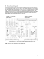
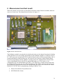
1
Design of a channel board used in an
electronic warfare target simulator
Examensarbete utfört i Elektroniksystem
av
Peter Andersson
LiTH-ISY-EX--06/3865--SE
Linköping 2006
Design of a channel board used in an
electronic warfare target simulator
Examensarbete utfört i Elektroniksystem
vid Linköpings tekniska högskola
av
Peter Andersson
LITH-ISY-EX--06/3865--SE
Handledare: Jesper Bäckstedt, Saab Bofors Dynamics
Examinator: Kent Palmkvist, ISY, Linköpings Universitet
Linköping 2006-09-08
Presentationsdatum
Institution och avdelning
Institutionen för systemteknik
2006-10-02
Publiceringsdatum (elektronisk version)
Department of Electrical Engineering
Språk
Typ av publikation
Svenska
X Annat (ange nedan)
Licentiatavhandling
X Examensarbete
C-uppsats
D-uppsats
Rapport
Annat (ange nedan)
Engelska
Antal sidor
61
ISBN (licentiatavhandling)
ISRN LiTH-ISY-EX--06/3865--SE
Serietitel (licentiatavhandling)
Serienummer/ISSN (licentiatavhandling)
URL för elektronisk version
http://www.ep.liu.se
Publikationens titel
Design of a channel board used in an electronic warfare target simulator
Författare
Peter Andersson
Sammanfattning
A channel board was designed for a DRFM circuit. The DRFM is implemented in a Virtex-4 FPGA from Xilinx. In the
future a similar channel board is intended to be used for target echo generation in ELSI which is an electronic warfare
simulator at Saab Bofors Dynamics in Linköping.
Besides the DRFM circuit the channel board consists of analog-to-digital converters, digital-to-analog converters, Ethernet
plug-in board with a microcontroller, voltage regulators, FPGA configuration memory, voltage amplifiers, current
amplifiers, oscillator, buffers/drivers and bus transceivers. The sample rate is 200 MHz and LVDS signalling standard is
used between the DRFM circuit and the converters.
The channel board has a JTAG interface which enables in-system programming of the FPGA. This implies that the DRFM
can easily be redesigned. An external computer can manage the channel board via Ethernet. Software was developed for the
microcontroller on the channel board and for the external computer. The function of the channel board is heavily dependent
on the DRFM circuit.
The channel board design resulted in the assembly of a prototype circuit board. Measurements were performed in a lab and
the channel board was approved to be integrated in ELSI for further tests.
Nyckelord
Saab Bofors Dynamics, Electronic Warfare Simulator, Target echo generation, Circuit board, DRFM, FPGA,
Microcontroller, Ethernet
Abstract
A channel board was designed for a DRFM circuit. The DRFM is implemented in a Virtex-4
FPGA from Xilinx. In the future a similar channel board is intended to be used for target echo
generation in ELSI which is an electronic warfare simulator at Saab Bofors Dynamics in
Linköping.
Besides the DRFM circuit the channel board consists of analog-to-digital converters, digitalto-analog converters, Ethernet plug-in board with a microcontroller, voltage regulators, FPGA
configuration memory, voltage amplifiers, current amplifiers, oscillator, buffers/drivers and
bus transceivers. The sample rate is 200 MHz and LVDS signalling standard is used between
the DRFM circuit and the converters.
The channel board has a JTAG interface which enables in-system programming of the FPGA.
This implies that the DRFM can easily be redesigned. An external computer can manage the
channel board via Ethernet. Software was developed for the microcontroller on the channel
board and for the external computer. The function of the channel board is heavily dependent
on the DRFM circuit.
The channel board design resulted in the assembly of a prototype circuit board. Measurements
were performed in a lab and the channel board was approved to be integrated in ELSI for
further tests.
Acknowledgements
Thank you all at Saab Bofors Dynamics in Linköping for taking good care of me during my
thesis work. I have enjoyed it very much and it has been a valuable experience for me.
I especially want to thank those at SBD who have been involved in my thesis work:
•
My supervisor Jesper Bäckstedt, for help with the circuit diagram and measurements.
•
Anna Goman, for making necessary modifications in the DRFM design and for the
correction of errors in my report.
•
Leif Tranell, for help with software tools.
•
Anders Nyhlén and Sture Carlson, for explaining how ELSI works.
•
David Svensson, for making the layout of the channel board.
•
Ulf Malmqvist, for guiding me through problems and for managing the project.
I also want to thank my examiner Kent Palmkvist at the Division of Electronics Systems,
Department of Electrical Engineering at Linköping University for comments on the report.
Abbreviations and acronyms
ADC
CPU
DAC
DC
DNS
DRFM
ECM
ELSI
EMI
ESL
ESR
FPGA
GPIO
IDE
I/O
JTAG
LED
LSB
LVCMOS
LVDS
MSB
NNDK
PC
PCB
PROM
RF
SBD
SDRAM
TBD
TCP/IP
UDP
VCCO
VME
Analog-to-Digital Converter
Central Processing Unit
Digital-to-Analog Converter
Direct Current
Domain Name System
Digital Radio Frequency Memory
Electronic Countermeasure
Electronic Warfare Simulator
Electromagnetic Interference
Equivalent Series Inductance
Equivalent Series Resistor
Field Programmable Gate Array
General Purpose Input/Output
Integrated Development Environment
Input/Output
Joint Test Action Group
Light-Emitting Diode
Least Significant Bit
Low Voltage Complementary Metal Oxide Semiconductor
Low Voltage Differential Signalling
Most Significant Bit
NetBurner Network Development Kit
Personal Computer
Printed Circuit Board
Programmable Read Only Memory
Radio Frequency
Saab Bofors Dynamics
Synchronous Dynamic Random Access Memory
To Be Decided
Transmission Control Protocol / Internet Protocol
User Datagram Protocol
Output drive voltage
Versa Module Eurocard
Table of contents
1
2
Introduction ................................................................................................................................................. 1
1.1
Background .......................................................................................................................................... 1
1.2
Aim ....................................................................................................................................................... 1
1.3
Organization ........................................................................................................................................ 1
1.4
About this report .................................................................................................................................. 2
ELSI system overview ................................................................................................................................. 3
2.1
3
Lab environment .................................................................................................................................. 4
Circuit board design.................................................................................................................................... 7
3.1
Software tools....................................................................................................................................... 7
3.2
Channel board overview ...................................................................................................................... 7
3.3
Xilinx Virtex-4 FPGA........................................................................................................................... 8
3.3.1
I/Os and banks................................................................................................................................. 9
3.3.2
Configuration .................................................................................................................................. 9
3.4
NetBurner Mod 5282 ........................................................................................................................... 9
3.5
Analog to digital conversion .............................................................................................................. 10
3.5.1
Differential amplifier..................................................................................................................... 10
3.5.2
Anti-aliasing filter ......................................................................................................................... 11
3.5.3
Non-inverting amplifier................................................................................................................. 12
3.5.4
Single-ended to differential conversion......................................................................................... 13
3.5.5
Analog-to-digital converter ........................................................................................................... 13
3.6
Digital to analog conversion.............................................................................................................. 14
3.6.1
Digital-to-analog converter ........................................................................................................... 14
3.6.2
Differential amplifier..................................................................................................................... 15
3.6.3
Reconstruction filter...................................................................................................................... 15
3.6.4
Non-inverting amplifier................................................................................................................. 17
3.7
Translators and bus transceivers ....................................................................................................... 17
3.8
DC/DC regulators.............................................................................................................................. 17
3.8.1
Current estimation ......................................................................................................................... 18
3.9
Component selection .......................................................................................................................... 19
3.9.1
Xilinx Virtex-4 FPGA................................................................................................................... 19
3.9.2
ADC and DAC .............................................................................................................................. 19
3.9.3
OP Amplifiers ............................................................................................................................... 20
3.9.4
Capacitors...................................................................................................................................... 20
3.9.5
DC/DC regulators.......................................................................................................................... 21
3.9.6
Translators and bus transceivers.................................................................................................... 22
4
5
Circuit board layout .................................................................................................................................. 23
4.1
LVDS (Low Voltage Differential Signalling) ..................................................................................... 24
4.2
Ground and power planes.................................................................................................................. 25
4.3
Layout recommendations ................................................................................................................... 25
Software applications ................................................................................................................................ 27
5.1
Platform NNDK ................................................................................................................................. 27
5.2
Choise of network protocol ................................................................................................................ 27
5.3
Channel board command format ....................................................................................................... 28
5.4
Netburner application ........................................................................................................................ 28
5.4.1
NetBurner/DRFM interface........................................................................................................... 29
5.4.2
Application flow............................................................................................................................ 30
6
5.5
PC application ................................................................................................................................... 31
5.6
Performance test ................................................................................................................................ 32
Measurement and test result .................................................................................................................... 33
6.1
Command format check-up ................................................................................................................ 34
6.2
Function test of channel board .......................................................................................................... 37
6.2.1
Read and write to DRFM .............................................................................................................. 37
6.2.2
Channel board basic functions ...................................................................................................... 37
6.2.3
Channel board RF output .............................................................................................................. 38
6.2.4
Channel board RF input ................................................................................................................ 39
6.2.5
Delay measurements ..................................................................................................................... 40
6.2.6
Varying distance to target ............................................................................................................. 42
6.2.7
Bandwidth ..................................................................................................................................... 42
6.2.8
The DAC problem......................................................................................................................... 43
7
Evaluation .................................................................................................................................................. 45
7.1
Learning’s from the project ............................................................................................................... 46
References............................................................................................................................................................ 47
A.
Requirement specification ........................................................................................................................ 49
B.
Time plan.................................................................................................................................................... 59
C.
PC application user manual...................................................................................................................... 61
1 Introduction
1.1 Background
Saab Bofors Dynamics (SBD) has many years of experiences of developing advanced defence
systems. SBD is one of the high-technology companies that have designed parts to the
European missile project METEOR. SBD is among other things developing radar target
seekers for missile applications. The radar target seekers are tested in ELSI (Electronic
Warfare Simulator) located at SBD in Linköping. ELSI is constantly upgraded to meet the
requirements of future generations of target seekers. For example the DRFM circuit has been
upgraded in ELSI. The DRFM circuit receives signals from the target seeker. Radar responses
are transmitted after variable delays, to simulate target distances for the seeker. When ELSI
first was designed by SBD the DRFM was implemented in a high speed ASIC. Since the
FPGA technology advances, the DRFM with increased functionality has been implemented in
an FPGA. Because the DRFM is implemented in an FPGA it simplifies redesign and lower
the cost associated with a change in the design. The DRFM design was created by a student as
a thesis project. The thesis report, LiTH-ISY-EX--05/3742--SE, is available at Linköping
Technical University website. A prototype circuit board for the DRFM circuit needs to be
designed before any target echoes can be generated and measured. SBD has decided that the
design of the circuit board is suitable for a thesis project.
1.2 Aim
The aim with this thesis project is to design a prototype circuit board (channel board) for the
DRFM. However the layout of the channel board shall be designed by a layout designer at
SBD. The PCB shall be manufactured and the channel board shall be assembled by an
electrician assembler at SBD. The channel board shall be managed from an external computer
through an Ethernet connection. Software applications to be run on the channel board and on
the external computer shall be written for the Ethernet communication. Measurements shall be
performed to verify the function of the channel board and the DRFM.
1.3 Organization
The intention was to carry out the thesis work as a project at SBD in Linköping. Requirement
specification and a time plan were written. Meetings have been arranged to follow up the
situation of the project. Regular attendees of the meetings were:
Peter Andersson, Thesis worker (writer of this report)
Jesper Bäckstedt, Supervisor (SBD)
Anna Goman, FPGA designer (SBD)
Sture Carlson, ELSI systems engineer (SBD)
Anders Nyhlén, ELSI systems engineer (SBD)
Gerth Karlsson, ELSI program manager (SBD)
Ulf Malmqvist, Electronic design manager (SBD)
The project shall result in a written report and an internal presentation shall be held at SBD.
1
1.4 About this report
Below is a short description of the chapters in this report.
Chapter 2, ELSI system overview, describes the function of the channel board and the ELSI
system where the channel board is intended to be located.
Chapter 3, Circuit board design, describes the channel board design. Components with
reference to datasheets are present.
Chapter 4, Circuit Board layout, is a brief description of design techniques for the printed
circuit board layout. The layout of the resulting channel board is shown.
Chapter 5, Software applications, describes the DRFM interface to Ethernet.
Chapter 6, Measurement and test result, captures an Ethernet frame and performs
measurements on the channel board.
Chapter 7, Evaluation, presents the result of the project and experiences from the project.
The appendixes contain the requirement specification, time plan and a brief user manual for
the application run on the external computer.
2
2 ELSI system overview
This chapter describes the ELSI (Electronic Warfare Simulator) system which the channel
board is intended to be operating in.
ELSI is used to test radar target seekers. The radar target seeker is a device mounted in the
front of a missile. When the missile is getting close to the selected target the target seeker
begins to transmit radar beams. When a radar beam is reflected back to the seeker a target is
found. The seeker then guides the missile to the target.
ELSI is a hardware in the loop simulator which means that the tested radar target seeker is
mounted in the simulator and presented with a radar scenario. The target seeker is operating
like if it was a part of a real missile flying in the air. The target seeker cannot distinguish
between the simulated scenario and a real scenario. When the target seeker transmits radar
beams the simulator presents a radar scenario containing targets and electronic
countermeasures. Electronic countermeasures are false targets which purpose is to spoof the
target seeker so the missile is guided away from the real target. The target seeker shall be
placed in the flight motion simulator in figure 2.1. The picture is taken from ELSI
presentation [27]. The flight motion simulator tricks the target seeker to believe that it is
located in a flying missile.
The room (anechoic chamber) where the target seeker is placed has the walls, floor and
ceiling covered with radar absorbing material, see figure 2.1. The absorbing material makes
the surfaces in the room invisible to the target seeker. The target seeker can only see the radar
response from the antennas in the room which generates the radar scenario. The antennas are
mounted on the opposite wall which is not shown in the figure.
Figure 2.1 The room (anechoic chamber) in ELSI where the target seekers are tested.
3
Before the radar response can be transmitted from the antennas the target echoes must be
generated. The target echoes are used to simulate radar beam reflections on targets. The target
echoes are generated by the DRFM circuit on the channel board. There are two methods to
generate target echoes.
The radar beams transmitted from the target seeker can be received by the antennas and
sampled by the channel board and stored in the DRFM circuit. Depending on the radar
scenario which shall be presented for the target seeker the radar beam can be delayed before it
is transmitted back to the target seeker. The delay is variable and corresponds to the target
distance seen by the target seeker. The delay can for example be decreased in real time during
simulation to simulate a shorter distance to the target. The simulated target distance is
calculated as:
Target distance =
speed of light × delay
2
The second method can be used when the waveform of the radar beam transmitted from the
target seeker is known. The waveform can then be stored in advance in the DRFM memory.
This method requires that a trigger signal from the target seeker is sent at the same instant as
the radar beam is transmitted. The radar response is transmitted after a delay corresponding to
the target distance.
Before the channel board samples the radar beam from the target seeker, the radar beam must
be converted to a lower frequency which the channel board can handle. The channel board
samples with 200 MHz so the converted frequency must be lower than 100 MHz to avoid
anti-aliasing effects. The radar beam is converted back to the original frequency before it is
transmitted from the antennas.
During simulation, data from the target seeker is stored in a computer. The data is matched
with the simulation scenario to analyze the actions of the target seeker.
2.1 Lab environment
Before the channel board can be integrated in ELSI the channel board shall be tested in the lab
environment shown in figure 2.2. The lab system is simple compared to the ELSI system
which is extremely advanced. An overview of the lab environment is more suitable to
describe the functions of the channel board. However the function of the channel board is
identical in both systems.
The signal generator simulates the radar target seeker and the oscilloscope is used to measure
the response from the channel board. The channel board has a connection to Ethernet through
which the delay can be changed in real time from an external computer during target
generation. Waveforms can also be downloaded over Ethernet from the external computer.
In fact all communication between the channel board and the external computer is carried out
over Ethernet.
The DRFM memory has an address and a data bus interface which can be accessed from the
external computer through Ethernet. The external computer can read and write to the DRFM
address range. The behaviour of the DRFM circuit is controlled by writing data to specific
4
addresses in the DRFM memory from the external computer. The data can for example
consist of delay values, waveforms and various commands.
Oscilloscope
RF and digital signals
Channel
Board
Ethernet cable
Ethernet
Network
Connection
Ethernet cable
External
Computer
RF or trigger signal
Signal
Generator
Figure 2.2 System overview of the lab environment.
5
6
3 Circuit board design
The purpose with this chapter is to describe the circuit board design. The created schematic
pages are most suitable for A3 format. Copying and displaying them in this report is therefore
not feasible. Therefore only selected parts from the schematic are displayed and they have
been drawn in Paint with fewer details to better fit the format of this report. However the
original schematic is filed in the SBD archive in Linköping.
Drawing name: ELSI MEG
Drawing number: 3500340-148
3.1 Software tools
The tools used to accomplish the circuit design are:
•
•
•
Design Architect, from Mentor Graphics
Matlab, from The MathWorks
Tina-Ti, from DesignSoft
The most important tool is Design Architect in which the schematic has been drawn. All
physical components used in the design are tied to symbols in Design Architect. The symbols
are created by a layout designer at SBD. Matlab was used to create sample data for a
sinusoidal pulse. Some minor simulations of the analog parts have been made with Tina-Ti.
Tina-Ti is a free special version of the Tina product preloaded with Texas Instruments (TI)
models. This free version is limited to small designs. Tina-Ti can be downloaded from TI
website [6].
3.2 Channel board overview
Figure 3.1 shows an overview of the channel board. The main component is the DRFM
circuit. The DRFM is a high speed memory used to store and transmit the delayed waveform.
The channel board consists of two independent channels A and B. Both channels have analog
input and output. The RF signals received at the analog inputs are sampled with 200 MHz to
differential 12-bit parallel words respectively. Channel B has besides the analog input and
output also a parallel 16-bit digital input and output. This means that either is the analog or
digital input directed to the outputs of channel B. The analog and digital outputs of channel B
are active simultaneously. The DRFM generates differential 200 MHz and 400 MHz clocks
from a 50 MHz oscillator. A 400 MHz clock is needed since the digital-to-analog converter
updates the analog output at half the input clock rate.
The waveforms can be recorded from the analog inputs or be downloaded from an external
computer on the Ethernet through the NetBurner module to the DRFM. Each channel also has
some additional digital inputs and outputs. Both channels can independently of each other
receive a trigger signal which indicates to the DRFM that it shall transmit a stored waveform.
After a delay measured from the received trigger signal the waveform is transmitted. The
length of the delay can be updated in real time from an external computer. The channels can
also transmit signals used to trig external ECM sources.
7
RF In A
RF In B
2×[11:0]
Analog
to digital
conversion 2×[11:0]
200 MHz
Digital In B
[15:0]
Inputs A
Translate
from
5V
to 3.3V
2×[11:0]
DRFM
Xilinx
Virtex - 4
FPGA
Digital
to analog
conversion
2×[11:0]
RF Out A
RF Out B
400 MHz
Translate
from
3.3V
to 5V
Inputs B
Digital Out B
[15:0]
Outputs A
Outputs B
50 MHz
Oscillator
Bus transceivers
NetBurner Mod 5282
(includes a
microcontroller)
5V
GND
DC/DC
regulators
-5 V
1.2 V
1.8 V
2.5 V
3.3 V
Nonvolatile
configuration
memory
(Flash)
JTAG
Ethernet
Voltage levels needed by
circuits on the channel board
Figure 3.1 Channel board overview.
3.3 Xilinx Virtex-4 FPGA
The DRFM design is implemented in an FPGA. The FPGA belongs to the Virtex-4 family
which is a new generation FPGA from Xilinx.
8
3.3.1 I/Os and banks
Virtex-4 family supports many I/O standards see, Virtex-4 User Guide [9]. The specific I/O
standards used are LVCMOS33 and LVDS25 which are 3.3 V single-ended and 2.5 V
differential I/O standards respectively. Virtex-4 devices are divided up into physical areas
denominated banks. Each user I/O pin belongs to a specific bank. Number of banks depends
on the device size. The banks can consist of different number of user I/O pins. Besides the
user I/O pins the bank consists of a number of output drive voltage pins denominated VCCO.
For example if a 3.3 V I/O standard is used in a bank all VCCO pins belonging to that bank
should be connected to 3.3 V. This means that only I/O standards with the same voltage levels
can be used in the same bank. Consequently LVCMOS33 and LVDS25 can not be used in the
same bank.
About one third of the available user I/O pins are used. To decrease power supply disturbance
when multiple output drivers change state, the used I/O pins are distributed over all available
banks in the device. The package pinout diagrams for the Virtex-4 family and a description of
the pins is available in Virtex-4 Packaging and Pinout Specification [8]. Notice that not all
user I/O pins support LVDS outputs. The method used when assigning signals to user I/O pins
is that signals with similar functions are assigned to user I/Os in the same bank. No layout
considerations have been made when arranging the signals within a separate bank. There are
640 user I/Os of a total of 1148 pins in the selected package. The remainder of the pins does
not belong to a specific bank. These pins are dedicated to power supply for the internal core
logic and auxiliary circuits.
3.3.2 Configuration
Virtex-4 internal configuration memory is volatile and must be configured at power-up. This
is done by loading the design configuration data into memory. The design configuration data
can be loaded through the JTAG interface pins or through dedicated configuration interface
pins.
In Virtex-4 Configuration Guide [11] several configuration methods are described. The
chosen configuration method is to connect a Xilinx configuration PROM to the Virtex-4
device. With this solution the Virtex-4 device will be configured automatically by the PROM
at power-up. The chosen PROM XCF32P belongs to the Platform Flash series of In System
Programmable Configuration PROM from Xilinx. See data sheet Platform Flash In-System
Programmable Configuration PROMS [12]. These PROMS can be connected to the dedicated
configuration pins on a Virtex-4 device and at the same time be connected in a JTAG chain
with the device. The PROM and the Virtex-4 device can be programmed in-system through
the JTAG interface using Xilinx IMPACT software and a Xilinx programming cable. Insystem means that the PROM and the Virtex-4 device don’t have to be removed from the
channel board when programmed. This is because the programming cable is connected to a
JTAG socket on the channel board. At power-up the PROM configures the Virtex-4 device
through the dedicated configuration pins. The dedicated configuration pins supports several
configuration modes. The PROM supports serial and 8-bit parallel configuration. The 8-bit
parallel configuration mode is chosen due to speed. The name of the mode is Master
SelectMAP in which the Virtex-4 device generates the configuration clock.
3.4 NetBurner Mod 5282
The NetBurner Mod 5282 module from the NetBurner company is used to “network-enable”
the channel board with 10/100 Ethernet. It was decided that the NetBurner module should be
used before this project started. The module is placed as a daughter board in two sockets on
9
the channel board. The module contains the Motorola ColdFire 5282 microcontroller, 8 MB
of SDRAM, Ethernet Port RJ-45 and an Ethernet transceiver. The microcontroller has a 66
MHz 32-bit architecture with integrated Fast Ethernet Controller and 512 KB of integrated
flash memory. Many of the microcontroller I/Os are available on two 50 pin connectors on the
module. These signals include the external 16-bit address and 16-bit data bus, chip selects and
many other signals that can be used as GPIO.
The microcontroller on the NetBurner module is the only processor on the channel board. The
microcontroller pins provide an interface to the DRFM circuit. Waveforms and commands
which control the function of the DRFM can be downloaded from an external computer on
Ethernet to the microcontroller on the NetBurner module. The microcontroller passes the
waveforms and the commands to the DRFM.
The NetBurner module supports software update through Ethernet.
3.5 Analog to digital conversion
Figure 3.2 shows the block diagram of the analog to digital conversion in figure 3.1. The
block is named after its main function. Only one channel is shown since the A and B channel
are identical.
RF In
Differential
amplifier
Antialiasing
filter
Noninverting
amplifier
Single-ended
to
differential
conversion
Analog-todigital
converter
To
DRFM
Figure 3.2 Block diagram for analog to digital conversion in figure 3.1.
The board traces (conducting paths for signals on a circuit board) characteristic impedance
relative the ground plane are designed to be 50 Ω by a layout designer at SBD. Termination
resistors of 50 Ω are therefore used to match the board traces. The termination resistors are
marked with 50 Ω in the following figures.
3.5.1 Differential amplifier
A signal source referenced to a local ground should be connected to a differential input
according to Connecting Single Ended and Differential Analog Inputs [14]. This is to avoid
ground loops caused by a difference in ground levels between signal source and in this case
the channel board. Figure 3.3 shows the differential amplifier at the analog input on the
channel board. The RF generator impedance (50 Ω) and the 50 Ω termination at the
differential amplifier input form a voltage divider. The voltage divider halves the signal
amplitude and for that reason the differential amplifier has the gain 2.
10
Shield coaxial cable
50 Ω
50 Ω
RF signal
50 Ω
RF generator
Local ground
Ground plane
Figure 3.3 Differential amplifier.
3.5.2 Anti-aliasing filter
Signals above half the sampling frequency are aliased (folded) into the band of interest when
sampling. This leads to that the analog signal cannot be reconstructed. The analog antialiasing filter bandlimits the input signal to limit the aliasing effect. The bandlimited analog
input signal can then be reconstructed by the reconstruction filter. In reality the unwanted
signals above half the sampling frequency cannot be completely eliminated. The anti-aliasing
filter shall have enough attenuation above half the sampling frequency so the reconstructed
signal has acceptable distortion. The sampling frequency is settled to be 200 MHz so the
attenuation shall be sufficiently above 100 MHz. In this project there are no requirements on
the attenuation in the stopband. This means that the attenuation can be chosen arbitrary.
However the channel board used in the simulator today has a 5th order Butterworth antialiasing filter. For the prototype channel board a 5th order Cauer filter was designed. The
filter topology is a doubly terminated LC ladder structure of π-type which is shown in figure
3.4. Source and load termination resistors are left out since they belong to the differential
amplifier respectively the single-ended amplifier.
Ground plane
Figure 3.4 Anti-aliasing filter.
The 3-dB bandwidth shall be 80 MHz according to the requirement specification in appendix.
The stopband edge is chosen to 100 MHz because it is half the sampling frequency. Notice
that the stopband edge also could be chosen to 120 MHz since the noise in the frequency band
100-120 MHz is aliased into the transition band 80-120 MHz which has no attenuation
requirement.
11
The filter specification is:
Passband cutoff frequency: 76 MHz
Ripple in the passband: 0.01 dB
Stopband edge: 100 MHz
Minimum attenuation in stopband: 25 dB
The filter specification results in about 3 dB attenuation at 80 MHz. The passband cutoff
frequency in the filter specification is lower than the 3-db bandwidth since the ripple is only
0.01 dB. The filter specification inserted in Matlab function ellipord returns the wanted filter
order 5. Matlab function CauerLCnet from Linköping Technical University filter toolbox
calculates the component values of the anti-aliasing filter. The component values are rounded
to standard values. The magnitude response based on standard values is shown in figure 3.5.
The simulation is carried out in the Tina-Ti software. The attenuation at low frequencies is
due to a series capacitor before the filter in the original circuit diagram. The signal attenuation
of 6-dB in the passband is due to the voltage divider formed by the two 50 Ω termination
resistors.
Figure 3.5 Magnitude response of the anti-aliasing filter with a series capacitor before the filter.
3.5.3 Non-inverting amplifier
The amplifier is used to adjust the signal voltage level to fit the analog-to-digital converter.
Figure 3.6 shows that the amplifier has a non-inverting gain configuration. The 50 Ω
termination resistors at the differential amplifier output and at the non-inverting amplifier
input form a voltage divider. Further the 50 Ω termination resistor at the non-inverting
amplifier output and the two 25 Ω termination resistors at the transformer in figure 3.7 form a
voltage divider. An amplifier gain of 4 cancels out the two voltage dividers. The result is that
the differential input voltage at the analog-to-digital converter is equal to the voltage at the RF
generator source in figure 3.3.
12
50 Ω
50 Ω
Ground plane
Figure 3.6 Non-inverting amplifier.
3.5.4 Single-ended to differential conversion
The analog-to-digital converter requires a differential input signal for best performance, see
figure 3.8. Differential input only requires half the signal swing on each input compared to a
single-ended input. Differential input also has superior common mode rejection compared to a
single-ended input. A wideband RF transformer from Mini-Circuits is used to convert the
single-ended signal to a differential signal. The conversion circuit is shown in figure 3.7.
25 Ω
25 Ω
Ground plane
Ground plane
Figure 3.7 Single-ended to differential circuit.
3.5.5 Analog-to-digital converter
The ADC is a device that samples the analog input signal and converts each sample into a
digital code. Nyquist sampling theorem states that the sample rate must be larger than double
the highest frequency in the analog signal to be able to reconstruct the analog signal. The
digital codes represent a limited number of discrete values of the analog signal. This
introduces quantization errors which is the difference between the voltage level the digital
code represents and the analog signal. In reality the analog signal cannot be completely
reconstructed due to quantization errors.
The ADC on the channel board has a differential input, see figure 3.8. Maximum allowed
peak-to-peak differential input voltage is 1.454 V according to the ADC datasheet [13].
Assume that an RF generator with 50 Ω impedance is connected to the input on the channel
board as in figure 3.3. If the RF signal has 0.7 V amplitude at the generator, the resulting
differential amplitude at the ADC input is 0.7 V. Consequently the peak-to-peak differential
voltage at the ADC input is 1.4 V and the maximum allowed amplitude at the RF generator
13
source is approximately 0.7 V. The ADC has a single 1.8 V supply and the analog inputs are
therefore self-biased to a common mode voltage.
Peak-topeak
differential
voltage
ADC
Figure 3.8 Differential signal at ADC input.
3.6 Digital to analog conversion
Figure 3.9 shows the block diagram of the digital to analog conversion in figure 3.1. The
block is named after its main function. Only one channel is shown since the A and B channel
are identical.
From
DRFM
Digital-toanalog
converter
Differential
amplifier
Reconstruction
filter
Noninverting
amplifier
RF Out
Figure 3.9 Block diagram for digital to analog conversion in figure 3.1.
The termination resistors which are used to match the characteristic impedance of the board
trace are marked with 50 Ω in the following figures.
3.6.1 Digital-to-analog converter
The DAC is a device that converts the digital codes (samples) at the input into an analog
signal at the output. The analog signal looks like a staircase since each digital code
corresponds to a voltage level which is kept constant between the samples. Figure 6.7 shows a
staircase signal measured with an oscilloscope after the digital-to-analog converter on the
channel board. The digital-to-analog converter on the channel board has a differential current
output. This means that the sum of the two currents are constant, see figure 3.10. Resistors at
the output convert the currents into a differential voltage. The currents result in a maximal 0.5
V peak-to-peak differential voltage. A digital word representing zero amplitude results in two
10 mA currents which result in a 0.25 V common mode voltage.
14
Ground plane
25 Ω
0 to 20 mA
DAC
50 Ω
20 to 0 mA
25 Ω
Ground plane
Figure 3.10 DAC differential output.
3.6.2 Differential amplifier
The differential amplifier has the same topology as the differential amplifier in figure 3.3
except that the terminating resistance at the input is removed, see figure 3.11. The amplifier is
used to convert a differential signal to a single ended. Since there is no voltage divider formed
by termination resistors between the DAC output and the differential amplifier the gain equals
1.
50 Ω
Ground plane
Figure 3.11 Differential amplifier.
3.6.3 Reconstruction filter
The frequency spectrum of the staircase signal, created by the digital-to-analog converter, has
images of the spectrum of the analog signal before sampling. These images are due to the
transitions in the staircase signal. The images are repeated with the sampling frequency as
shown in figure 3.12.
15
0
100 MHz 200 MHz
400 MHz
600 MHz
Spectrum of the analog
signal before sampling
Figure 3.12 Frequency spectrum after digital-to-analog conversion.
The purpose of the reconstruction filter is to keep the spectrum of the analog signal and
attenuate the repeated images to obtain a smooth signal with much smaller staircase
transitions. The reconstruction filter is chosen to be a 5th order Cauer filter like the antialiasing filter in figure 3.4 but with a different filter specification:
Passband cutoff frequency: 70 MHz
Ripple in the passband: 0.01 dB
Stopband edge: 150 MHz
Minimum attenuation in stopband: 52 dB
The filter specification results in about 3 dB attenuation at 80 MHz. The simulated magnitude
response with standard component values is shown in figure 3.13. The attenuation at low
frequencies is due to a series capacitor before the filter in the original circuit diagram.
Figure 3.13 Magnitude response of the reconstruction filter with a series capacitor before the filter.
16
For simplicity the filter specification could have been the same as the anti-aliasing filter.
However it is better to test two different filters in the hardware if one should fail due to
improper component values.
3.6.4 Non-inverting amplifier
The non-inverting amplifier is exactly the same as in figure 3.6. A voltage divider is formed
by the termination resistors at the differential amplifier output and at the input to the noninverting amplifier. In addition a voltage divider is formed by the termination resistor at the
non-inverting amplifier output and the 50 Ω load resistor connected to the channel board
output. A gain of 4 cancels out the voltage dividers. The maximal peak-to-peak voltage at the
load is equal to the maximal differential peak-to-peak voltage after the digital-to-analog
conversion i.e. 0.5 V. The maximal allowed peak-to-peak voltage of 0.7 V over 50 Ω at the
channel board input results in 0.5 V peak-to-peak over a 50 Ω load connected to the channel
board output. According to the requirement specification in appendix A, the peak-to-peak
voltage at the 50 Ω load shall be 0.63 V to obtain 0 dBm. The resistors in the non-inverting
amplifier can be changed to fulfil the requirement. This should be done by measuring the
voltage at the load while changing the resistors.
3.7 Translators and bus transceivers
In the environment surrounding the channel board only 5 V logic is used. Virtex-4 FPGAs
don’t have 5 V I/O standards. However 3.3 V I/O standards are available. Therefore
translations between 5 V and 3.3 V are necessary. Devices used for translations are
buffers/drivers. In addition the buffers/drivers isolate the Virtex-4 FPGA and protect it from
electrostatic discharge. If a high voltage is applied by mistake to the channel board the
buffers/drivers take the damage. The FPGA is much more expensive than a buffer/driver to
replace.
Transceivers with tri-state ports are used between the FPGA and the NetBurner module to
isolate the FPGA from the address and data bus. The voltage level applied to the control
inputs on the transceiver sets the direction and tri-state option. No translation between voltage
levels is needed since the NetBurner module is a 3.3 V device.
3.8 DC/DC regulators
The channel board takes its power from a VME backplane. The VME backplane provides no
voltages lower than 5 V. This means that the channel board must contain DC/DC regulators
since -5 V, 1.2 V, 1.8 V, 2.5 V, 3.3 V and 5 V power supplies are needed by the circuits on
the channel board. Common for all regulators used are that they require a decoupling
capacitor between the output and ground to be stable. The minimum value of the output
capacitor is stated in the datasheet for each regulator.
Circuit datasheets usually recommend that decoupling capacitors should be placed both at the
power source (DC/DC regulator) and at the circuit as shown in figure 3.14. The decoupling
capacitors at the circuit shall be placed close to the power supply pins of the circuit. A
common used value is 100 nF and sometimes also 100 pF is recommended in the data sheets.
The decoupling capacitors supply the transient switching current to the circuit. This decreases
the voltage change in the power supply. If the voltage change is too large it can cause an
incorrect behaviour in the circuit. The capacitors at the regulator are much larger and are often
in the range 1-100 µF. Sometimes the values are not specified and they may be shared among
several devices according to datasheets. There is only one regulator for each voltage level on
the channel board which implies that circuits have to share the same regulator. Instead of
17
adding all the recommended decoupling capacitors in parallel at the regulators for each
circuit, only one was used. This was an attempt to decrease the number of decoupling
capacitors. Notice that the capacitor shall be larger than the minimum value required for the
regulator to be stable. The Virtex-4 (LX60) has around 200 power supply pins which are all
decoupled according to Virtex-4 PCB Designer’s Guide [16] page 43. The attempt above to
decrease the number of decoupling capacitors was insignificant due to all decoupling
capacitors needed for the Virtex-4 FPGA.
Vin
Vout
100 pF 100 nF
DC/DC
Regulator
Circuit
GND
Figure 3.14 Decoupling capacitors.
3.8.1 Current estimation
The current consumption for each voltage level on the channel board needs to be estimated.
The result is used to set requirements on the minimum output current that the regulators must
be able to deliver to the channel board. Figure 3.15 shows the estimated currents. All values
are fetched from the circuits datasheets.
1,8 V
2×ADC
2×DAC
Flash
3,3 V
2×DAC
NetBurner
Flash
Oscillator
Analog supply
current [mA]
2×390
2×31
Digital supply
current [mA]
2×64
2×33
Internal supply
current [mA]
10
Analog supply
current [mA]
2×52
+/– 5 V
6×Current-feedback OP
2×Voltage-feedback OP
Digital supply
current [mA]
500
40
20
Quiescent
current
[mA]
6×14
2×22
Total current
[mA]
104
500
40
20
664
Signal amplitude 1V
Load resistance 100Ω
Current 1000/100 [mA]
6×10
2×10
Figure 3.15 Estimated current consumption on the channel board.
18
Total current
[mA]
908
128
10
1046
Total current
[mA]
144
64
208
The Virtex-4 current consumption is design dependent and no information was available
when the current estimation was performed. Which Virtex-4 device to use was not determined
until later. The DRFM design also needed to be modified due to new requirements. The
current consumption in figure 3.16 is obtained from simulations by the FPGA design tool.
Notice that there is no information about the 3.3 V supply current. This is because a 2.5 V
single-ended I/O standard is used instead of the intended 3.3 V single-ended I/O standard. The
mistake was discovered late in the project and no incorrect behaviour has been detected.
Virtex-4
(LX60)
1,2 V
Internal supply
current [mA]
500
2,5 V
VCCO and auxiliary
supply current [mA]
557
3,3 V
VCCO supply
current [mA]
No information
Figure 3.16 Estimated current consumption for the Virtex-4 (LX60) device.
3.9 Component selection
The selection of components can be very time consuming since there are many producers.
Fortunately SBD has a database which contains all components used in previous projects
which narrows the search considerable. The first step is consequently to search in the database
and thereafter on producer’s web sites on the Internet. Only surface mounted components are
of interest.
3.9.1 Xilinx Virtex-4 FPGA
The DRFM design is designed to be implemented in a Xilinx Virtex-4 FPGA. The Virtex-4
family contains three family members: LX, FX and SX families. The DRFM design can be
implemented in any of these families assumed that they are large enough to store the design.
All families are available in different speed grades and a higher speed grade corresponds to a
faster device. For this project a Xilinx Virtex-4 LX60 device with speed grade 12 was chosen.
This is the smallest LX device which can store the DRFM design. The LX60 device is
available in two packages. The larger package was chosen which has 640 user I/Os of a total
of 1148 pins. The design uses about 235 user I/Os of which 205 user I/Os are essential for the
function of the design. The smaller package could have been chosen but the larger package
has according to Virtex-4 Family Overview [7] superior signal integrity. Virtex-4 devices are
exclusively available in flip-chip BGA packages. The selected package has a size of 35×35
mm and a pitch of 1 mm.
3.9.2 ADC and DAC
Only five producer’s web sites were visited to keep down the search of the converters. The
producer’s are Linear Technology, Analog Devices, National Semiconductor, Texas
Instruments and Maxim. The converters shall fulfil the following requirements:
•
•
•
•
Conversion rate 200 MHz
LVDS interface
Two’s complement data format
Resolution 12 bits
The chosen ADC and DAC were found at Maxim’s web site.
19
ADC: MAX1214
Datasheet: 1.8V, 12-bit, 210Msps ADC for Broadband Applications [13]
DAC: MAX5876
Datasheet: 12-bit, 250Msps, High-Dynamic-Performance, Dual DAC with LVDS Inputs [15]
3.9.3 OP Amplifiers
There are two types of operational amplifiers for high frequencies, voltage-feedback
amplifiers and current-feedback amplifiers. The voltage-feedback amplifier is characterized
by a constant gain bandwidth product. This means that if the gain is increased 10 times in a
non-inverting amplifier the bandwidth is decreased 10 times. Current-feedback amplifiers do
not have the dependency between gain and bandwidth as the voltage-feedback amplifier has.
The consequence is that current-feedback amplifiers can have high gain and high bandwidth
at the same time. The differential amplifier after the digital-to-analog converter has a low gain
of 1 and therefore a voltage-amplifier is used in that circuit. The remainder of the amplifiers
has a gain of 2 and a gain of 4. For these amplifier circuits a current-feedback amplifier is
more suitable. The voltage-feedback and current-feedback amplifiers were found in the SBD
database. Both amplifiers are from Texas Instruments.
Voltage-feedback amplifier: THS4271
Datasheet: Low Noise, High Slew Rate, Unity Gain Stable Voltage Feedback Amplifier [18]
Current-feedback amplifier: THS3201
Datasheet: 1.8-GHz, Low Distortion, Current Feedback Amplifier [17]
Notice in the datasheet that current-feedback amplifiers are very dependent on the feedback
resistor to achieve high bandwidth and stability.
3.9.4 Capacitors
There exist several capacitor types and which type to choose depends on the application
according to http://www.epanorama.net/links/componentinfo.html [19]. For RF applications
are ceramic capacitors the best choice. Ceramic capacitors have extremely low parasitic
effects such as ESR and ESL. ESR is an unwanted parasitic resistor in series with the
capacitor. ESR is frequency dependent and is equal to the sum of all parasitic resistances in
the capacitor. ESL is an unwanted parasitic inductor in series with the capacitor. There are
also different types of ceramic capacitors. The NPO type is a good choice for applications that
require small tolerances and stability against aging, temperature and frequency. The drawback
is that NPO is only available in small capacitance values. The capacitors in the filters on the
channel board are of NPO type. Another type is X7R which is a common ceramic. The 100 nF
decoupling capacitors are of X7R type. The decoupling capacitors that shall be placed close to
the analog and digital circuits are always recommended by the datasheets to be of ceramic
type.
When decoupling power supplies (regulators) much larger capacitors are needed. The most
common types are electrolytic and tantalum capacitors. Both are polarity sensitive and will be
damaged when placed in the wrong direction. The drawback of electrolytic capacitors is that
the wet electrolyte dries with time. The consequence is increased ESR and decreased
capacitance. Electrolytic capacitors also have high ESR. Therefore are tantalum capacitors
used as large decoupling capacitors and they are often recommended in datasheets.
20
3.9.5 DC/DC regulators
There are two types of voltage regulators, linear and switching regulators. The main
difference is that a linear regulator consumes more power than a switching regulator. In
addition a switching regulator generates more noise. Since there are no requirements on
power consumption linear regulators are preferred. The maximum output current from the
regulators was compared with the current estimation to secure that they can deliver enough
current. Only one regulator for each voltage level was chosen. Regulators for 1.2 V, 2.5 V and
3.3 V can supply 3 A or more to compensate for the Virtex-4 current consumption. The -5 V
switching regulator for the analog amplifiers can supply 1 A. The analog amplifiers also
require 5 V which is supplied from the VME backplane.
Regulator -5 V: PT5022C
Datasheet: Positive Input/Negative Output Integrated Switching Regulator [20]
Regulator 1.8 V, 2.5 V, 3.3 V: LT1764A
Datasheet: LT1764A-3A, Fast Transient Response, Low Noise, LDO Regulators [22]
Regulator 1.2 V: TPS54612
Datasheet: 3-V to 6-V Input, 6-A Output Synchronous Buck PWM Switcher with Integrated
FETs [21]
The total current from the 5 V power supply which supports all the regulators with current can
be estimated. For linear regulators the input current is equal to the output current. For
switching regulators the input power is equal to the output power except for an efficiency
factor, which can be found in the datasheets. The currents denominated Iout are equal to the
estimated total currents for each voltage level in figure 3.15 and 3.16. The calculations are:
1.2 V (Switching regulator)
Pin × Efficiency = Pout ⇔ Vin × I in × Efficiency = Vout × I out
Vin = 5 V, Efficiency = 0.9, Vout = 1.2 V, Iout = 500 mA ⇒
Iin = 0.14 A
1.8 V (Linear regulator)
I in = I out = 1.05 A
2.5 V (Linear regulator)
I in = I out = 0.56 A
3.3 V (Linear regulator)
I in = I out = 0.66 A
5 V (No regulator needed)
I in = I out = 0.21 A
-5 V (Switching regulator)
Pin × Efficiency = Pout ⇔ Vin × I in × Efficiency = Vout × I out
Vin = 5 V, Efficiency = 0.75, Vout = -5 V, Iout = -208 mA ⇒
Iin = 0.28 A
21
The sum of the Iin currents is 2.9 A. This is the estimated total current from the 5 V power
supply which is required for the channel board.
The total current consumed by the channel board was measured to 2.8 A. The estimated value
is a little high even though LEDs, buffers/drivers and bus transceivers have not been
considered in the estimation.
3.9.6 Translators and bus transceivers
The buffers/drivers that act as translators between voltage levels are from Texas Instruments.
Octal in the datasheet name means that there are 8 buffers/drivers in each circuit. The signals
can only pass the circuits in one direction. This explains why two different circuits are
needed. The transceivers on the address and data bus can pass signals in both directions.
5 V to 3.3 V: SN54LVCH244A
Datasheet: Octal Buffers/Drivers With 3-State Output [24]
3.3 V to 5 V: SN54ABT244
Datasheet: Octal Buffers/Drivers With 3-State Output [23]
Transceiver: SN54LVTH16245A
Datasheet: 3.3-V ABT 16-Bit Bus Transceivers With 3-State Outputs [25]
22
4 Circuit board layout
Designing board layout requires a lot of experience and therefore the layout was carried out
by a layout designer at SBD. The Virtex-4 device has 1148 pins distributed on a size of 35×35
mm which implies that it can be difficult to route the traces. The layout resulted in a ten layer
board. The layout of the component side of the channel board is shown in figure 4.1. The
board has a size of 160.0×233.4×1.6 mm and is made of FR4 material. Of the ten layers there
are 6 signal layers (two outside and four inside), one ground layer and three power layers.
Some statistics of the circuit board is shown in figure 4.2.
Channel A, B analog (RF)
inputs/outputs
Channel A, B digital
inputs/outputs
DAC
Reset button
ADC
FPGA
Flash
Socket for
NetBurner
module
VME connectors (5 V power supply, channel B digital input/output [15:0])
Figure 4.1 Layout of the component side of the channel board.
23
Circuit board statistics
Number of vias
Number of nets
Number of connections
Number of components
Total length of nets
Minimum distance between two traces
Minimum trace width
Minimum via diameter
Trace width 50 Ω traces
Minimum distance between 50 Ω traces
Trace width 100 Ω differential traces in a pair
Distance between the traces in a differential pair
Minimum distance between differential pairs
Distance between the outside signal layer and ground layer
Outside copper plane thickness (plating Ni/Au included)
Inside copper plane thickness
1774
546
2774
606
28853 mm
0.127 mm
0.127 mm
0.3 mm
0.2 mm
0.127 mm
0.1 mm
0.127 mm
0.127 mm
0.135 mm
0.045 mm
0.035 mm
Figure 4.2 Circuit board statistics
4.1 LVDS (Low Voltage Differential Signalling)
The interface between the analog-to-digital converter and the FPGA is 12-bit parallel and
each bit is transferred differentially. The same interface exists between the FPGA and the
digital-to-analog converter. The differential signalling used is LVDS.
An LVDS output is a current source which can change direction of the current through the
termination resistor at the differential input of the receiver. The directions correspond to the
logic states one and zero. The current is approximately 3.5 mA which leads to 350 mV
differential voltage across a 100 Ω termination resistor. A small voltage swing results in a fast
rise time which enables a high data rate.
In LVDS Owner’s Manual – 3rd Edition [26] there are some recommendations when
designing PCB boards for frequencies above 100 MHz. The two traces belonging to a
differential pair should be routed as close as possible. The minimum distance between traces
is dependent on the manufacturer of the PCB board. This minimizes the phase difference at
the receiver since the traces will get the same length. Noise picked up will be coupled as
common mode and consequently suppressed at the receiver. Traces close together will also
radiate less due to magnetic field cancellation. The differential pair shall have 100 Ω
differential characteristic impedance to match the 100 Ω differential termination at the
receiver.
The traces that carry the RF signals are designed to have 50 Ω characteristic impedance
relative to the ground plane. Both the 50 Ω traces and the 100 Ω differential pairs are located
on an outside layer with a ground layer below. If two 50 Ω traces are far separated from each
other they will have 100 Ω differential impedance coupled through the ground plane in the
channel board. Two traces in a differential pair are placed close together. This results in that
the width of the traces is smaller than the 50 Ω traces to achieve 100 Ω differential
characteristic impedance. This is due to the extra coupling through air between the wires
when placed close together.
24
4.2 Ground and power planes
The channel board consists of an analog and a digital ground plane joined at a single point.
This is an attempt to prevent large return currents from digital components to reach the analog
ground plane and cause a varying ground potential. The two ground planes share the same
layer directly beneath an outside signal layer on the channel board. The analog ground is
located below the analog circuits and the digital ground is located below the digital circuits.
Only a short trace and a via is needed to connect a circuit to its ground. In addition the
regulators on the channel board create digital -5 V, 1.2 V, 1.8 V, 2.5 V and 3.3 V from 5 V.
Some of the voltage levels from the regulators are passed through EMI filters to create an
analog version. The purpose of the EMI filter is to prevent noise on the digital power supply
to reach the analog power supply. Both the digital and analog version of all the different
voltage levels is assigned to a specific power plane. This resulted in that ten power planes are
divided up on three layers on the channel board. A circuit on the channel board shall have its
required power supplies on layers directly below the circuit. This results in that a short trace
and a via is needed to make a connection between the power supply pin of the circuit and a
power plane below the circuit.
4.3 Layout recommendations
The following layout recommendations are found in the datasheets for the circuits used on the
channel board.
•
•
•
•
•
•
•
The distance between the ceramic decoupling capacitors (100 nF, 100pF) and the
circuits power supply pins shall be minimized.
Decouple the supply voltages at the source with tantalum capacitors.
High speed OP amplifiers are very sensitive to parasitic capacitances. Therefore a
window should be cut out from the ground plane below each amplifier.
Components that require a thermal pad shall have vias with low thermal resistance
connected to the ground plane.
High speed signals should be run on traces directly above a ground plane.
Digital signal paths should be short and far away from sensitive analog signals.
Match the length of digital signals to avoid phase difference (skew mismatch).
25
26
5 Software applications
The software applications shall handle the Ethernet communication between the channel
board and the external computer. This means that it shall be possible to write data to DRFM
address range and read data from DRFM address range from the external computer. The
application for the external computer shall be run on an ordinary PC. The DRFM contains a
set of registers that controls the function of the DRFM. The application located in the
NetBurner module on the channel board shall be fast enough to update the DRFM registers at
a speed of 100 Hz.
5.1 Platform NNDK
When SBD decided to use the NetBurner module as Ethernet interface to the DRFM they also
decided to purchase NetBurner Network Development Kit (NNDK). The kit includes the
NetBurner Mod 5282 module and a carrier board for the module. It also contains a lot of
software for example the NetBurner TCP/IP Stack, the NetBurner Real-time Operating
System based on uC/OS, the GNU C/C++ compiler and linker and the NetBurner Dev C++
IDE (Integrated Development Environment). Additional software is the NetBurner IPSetup
Configuration Utility used to set the modules IP address, network mask, gateway and DNS
server. The configuration data is downloaded over Ethernet into the parameter area of the
flash in the microcontroller MCF5282 ColdFire situated on the module. The NetBurner
AutoUpdate Utility is used to download code over Ethernet to the application area of the
flash. The application is stored as a compressed image and the Boot Monitor in the flash
uncompresses the application and loads it into the SDRAM on the NetBurner module. Note
that the application always runs from SDRAM. The carrier board provides a COM port which
makes it easy to debug the applications. Applications in the NetBurner module can write
information to the COM port.
5.2 Choise of network protocol
According to the requirement specification the network applications shall be designed to use
both TCP and UDP protocols. However for simplicity only one protocol should be
implemented at the beginning. In the NetBurner Programming Guide [1] it is declared that the
NetBurner UDP Class implementation is 30 % faster than TCP. This is due to TCP copies the
data to buffers in contrast to UDP which provides a pointer to the data. Since the registers in
the DRFM shall be updated with 100 Hz, UDP is the best alternative. If the 100 Hz
requirement is not fulfilled with UDP neither it will be with TCP. The drawback is that UDP
has no flow control. The result is that the PC must wait between each transmission of a UDP
packet to make sure that the NetBurner application has finished processing the data. In
addition UDP does not sequence the UDP packets. On a large network such as Internet UDP
packets can travel different paths to the receiving computer. This can lead to that UDP
packets reaches the receiving computer in the wrong sequence. In this case the network is
local and there is only one way for the packets to travel to the receiving channel board so
using UDP does not lead to packets in wrong sequence. At last UDP has limited error control
and the transmitter will not know if the packet has reached its destination. However if the
UDP packet sent did not give the expected output from the DRFM the packet can be
retransmitted. In reality the packets are seldom incorrect and reach its destination in a local
network. However since it shall be possible to read from the DRFM memory the transmitted
data can be verified.
27
5.3 Channel board command format
A command format is needed so the NetBurner application can interpret data (commands)
transmitted over Ethernet from the PC. Since the NetBurner application is communicating
with the DRFM through an address and a data port it is convenient to implement address and
data fields in the command format. The command format should have information about how
many address and data fields the packet contains and if the addresses in DRFM shall be read
or written. Figure 5.1 shows the implemented command format in a UDP packet.
Number of addresses
2 bytes
Mode
2 bytes
Address
4 bytes
Data
4 bytes
Address
4 bytes
Data
4 bytes
Figure 5.1 Channel board command format over Ethernet.
The field descriptions are:
•
•
•
•
Number of addresses: Number of addresses with belonging data field in a packet sent
over Ethernet (2 bytes).
Mode: The value 1 indicates write to DRFM addresses and value 2 indicates read from
DRFM addresses (2 bytes).
Address: This is an address in the DRFM address range (4 bytes).
Data: Data to write to the address in the nearest preceding address field or when a read
command is transmitted arbitrary data which is ignored (4-bytes).
The fields are transmitted from the left to the right in figure 5.1 with MSB first in each field.
In 2-byte fields MSB is equal to bit 15 and LSB is equal to bit 0. In 4-byte fields MSB is
equal to bit 31 and LSB is equal to bit 0. For simplicity the command format is not repeated in
a UDP packet i.e. the DRFM addresses can not be read and written in the same packet. When
a UDP packet containing a read command is transmitted from the PC the data fields can
contain arbitrary values. The NetBurner application then transmits a UDP packet back to the
PC with the same content as the received UDP packet except that the content in the data fields
have been replaced with the data read from the DRFM.
5.4 Netburner application
Development of the NetBurner application was carried out in the NetBurner Dev C++ IDE
and the code was compiled and linked with the GNU C/C++ compiler and linker. The
application starts at a function called UserMain() which is a task created in the uC/OS
operating system files. Also an additional task is created but with a higher priority. The
uC/OS is a pre-emptive Real-Time Operating System. This means that the highest priority
task ready to run will always run. Tasks can not have the same priority as in Windows where
each task runs in time slices. Lower priority tasks can only run when a higher priority task is
blocked. A task is blocked when it calls a blocking function like a time delay or a function
that waits for a UDP packet to be received. There are many more blocking functions but they
are not used in this application.
Thus the application consists of two tasks. The task with the lowest priority only applies a
reset pulse to the DRFM after the DRFM is configured. This is done by checking the Done
pin on Virtex-4 (DRFM) which indicates when the DRFM is configured. The task with the
highest priority consequently does everything else, see the application flow section. Some of
the priority levels are reserved. The TCP/IP stack is integrated in the uC/OS system. The
28
TCP/IP stack task is a higher priority task and will interrupt the two tasks in the application
when to process network data.
NetBurner IP address is set with the IPSetup utility and listening port number is set in the
application. If DRFM is read, NetBurner application sends a UDP packet back to the source
IP address and port number of the received packet. The NetBurner module and the PC are part
of an existing network, therefore the IP addresses, network masks, gateways and DNS are
supplied by a network administrator.
5.4.1 NetBurner/DRFM interface
The chip select module in the microcontroller provides a method to read and write to external
I/O devices. In this case the external device is the DRFM. In the NetBurner Mod5282
memory map there is address space reserved for I/O. This means that the same address and
data bus is used to address both memory and I/O devices, and the CPU instructions used to
read and write to memory is also used to access I/O devices. The NetBurner communication
interface to the DRFM is shown in figure 5.2.
Signal name
Addr[17:0]
Data[16:0]
R/W
CS
Signal description
Address port.
Bits 16-17 are GPIO pins because the available external address
bus is only 16 bits. Bits 1-15 is from the external address bus. Bit
0 is a GPIO pin because odd addresses are not allowed when
using the 16-bit external data bus.
Data port.
Bit 16 is represented by two GPIO pins. One for read and one for
write to DRFM. Bits 0-15 are from the 16-bits external data bus.
Indicates to the DRFM if the address shall be read or written.
The chip select signal indicates to the DRFM that a data transfer
shall start.
Figure 5.2 NetBurner/DRFM communication interface signals.
Before a bus transfer can start between NetBurner and DRFM the chip select registers in the
microcontroller must be configured. The result is that when the DRFM is addressed a bus
transfer automatically takes place except for the GPIO signals which is handled manually.
The timing diagram for a write bus cycle is shown in figure 5.3. More information is
presented in MCF5282 ColdFire Microcontroller User’s Manual [2]. The I/O device can
indicate through a transfer acknowledge signal when data is stored on a write cycle or when
data is available on a read cycle. However chip select registers have been configured to enable
auto-acknowledge and therefore the external transfer acknowledge signal is not used because
it is generated internally in the microcontroller. How many clock cycles the microcontroller
shall insert before generating the internal transfer acknowledge is programmable in the chip
select registers. The clock signal in the basic read and write bus cycle is not used in the
interface because the DRFM uses its own 50 MHz clock. This implies that the DRFM waits a
few clock pulses until the data on the data port is valid before the data port is sampled on a
write cycle. The internal transfer acknowledge signal can be chosen to be generated at a
maximum of 15 clock cycles (microcontroller 66 MHz clock) after chip select signal is set.
Consequently there is plenty of time where the data port can be sampled by the DRFM to
make sure that the data is valid. At a read bus cycle the R/W signal is high and the
29
microcontroller waits until the internal transfer acknowledge signal is asserted before the data
port is sampled.
Addr[17:0]
Address valid
R/W
CS
Data[16:0]
Data valid
Figure 5.3 Write bus cycle timing diagram.
5.4.2 Application flow
The flow is as follows:
Repeat the following.
Create an instance of a packet to be received.
Wait until a packet is received.
If Mode is equal to write in received packet.
Repeat until the last address in received packet.
Write to DRFM.
If Mode is equal to read.
Create an instance of a packet to be sent back.
Copy the fields Number of addresses and Mode in received packet
to packet to be sent.
Repeat until the last address in received packet.
Read from DRFM.
Send the packet.
Write to DRFM:
Set one GPIO pin equal to bit 16 of the data field.
Set two GPIO pins equal to bits 16 and 17 of the address field.
Create chip select address from bits 0-15 of the address field.
If chip select address is odd
Set one GPIO pin high to indicate odd address.
Decrease chip select address by one.
else (chip select address is even)
Set the GPIO pin low to indicate even address.
Write bits 0-15 of the data field to the chip select address (DRFM).
30
Read from DRFM:
Set two GPIO pins equal to bits 16 and 17 of the address field.
Create chip select address from bits 0-15 of the address field.
If chip select address is odd
Set one GPIO pin high to indicate odd address.
Decrease chip select address by one.
else (chip select address is even)
Set the GPIO pin low to indicate even address.
Read data from the chip select address (DRFM) and store it as bits 0-15 in
the data field in the packet to be sent.
Store the GPIO pin value as bit 16 of the data field in the packet to be sent.
Copy the address field in the received packet to the address field in the packet to
be sent.
5.5 PC application
The application in the PC is written in Microsoft Visual Studio 2003 and compiled as a C++
Win32 console application. The main function sends UDP packets. A second function is
called as a thread which receives UDP packets and writes the content on the command line.
The same UDP socket is used to send and receive packets. This results in that the same port
number is used to send and receive packets which are necessary because NetBurner
application sends packets back to the source of the received packet. The PC application reads
2-byte and 4-byte words in hexadecimal notation from a text file, and sends the words in a
UDP packet to the NetBurner application. The content in the file is consistent with the chosen
command format. It is also possible to send the same packet a number of times which is used
in the performance test. Another feature of the application is that it writes repeatedly to the
delay register. A start value is decremented down to zero delay and then incremented back in
steps of one. The purpose is to simulate a varying distance to the target.
Processors used in PCs use “Little Endian” byte order which means that the least significant
byte in a multibyte number (LongInt, ShortInt) is stored in memory at the lowest address and
the most significant byte at the highest address. Processors like Motorola use “Big Endian”
byte order where the most significant byte is stored in memory at the lowest address and the
least significant byte is stored at the highest address. For more information take a look at the
Wikipedia website [3]. Because the PC application reads multibytes numbers from the file the
numbers need to be converted before sending the UDP packet to the NetBurner application
which is run on a Motorola processor.
To allow the NetBurner application to finish processing the received data, a delay is
implemented between each UDP transmission. The length of the minimum delay depends on
the size of the UDP packet and the size depends on the number of address and data fields. In
addition if the addresses are read then the delay need to be longer than if the addresses are
written because a UDP packet is sent back to the PC. Note that if the NetBurner application is
changed it might require the delay to be changed also. The PC has Microsoft Windows XP
installed and the processor is an Intel Pentium 2.4 GHz. The delay implemented is just a
simple loop so if the PC is exchanged the number of rounds the loop executes needs to be
modified. If the packets are sent to often, packets will be missed by the NetBurner
application.
31
5.6 Performance test
Some simple performance tests have been carried out when the NetBurner module was
situated on the NNDKs carrier board. This was possible since there is no handshaking in the
interface between the NetBurner and the DRFM. The result should be the same if the
NetBurner module was situated on the channel board. The PC application repeatedly sends
the same UDP packet in write mode to the NetBurner module. In the NetBurner application a
counter is implemented which counts the number of packets received and writes the sum
every tenth second to the serial port on the carrier board. The sum of the received packets is
viewed with a terminal program included in the NNDK on the PC. If the packets are sent to
often the counter will not count all the packets sent i.e. the number of received packets is less
than the number of sent packets. Two different sizes on the packets were sent each hundred
thousand times. With a packet size of 10 addresses a speed of approximate 2400 packets per
second was achieved without loss of packets and a size of 160 addresses resulted in a speed of
550 packets per second. The conclusion is that it is possible to update the DRFM registers at a
speed of 100 Hz since the number of registers is less than 160.
32
6 Measurement and test result
When the printed circuit board was manufactured and the channel board assembled, hardware
tests were carried out. The channel board is shown in figure 6.1.
Figure 6.1 The channel board.
The NetBurner module was placed in the dedicated socket on the channel board and a flashing
LED application was successfully downloaded to the NetBurner module over Ethernet from a
PC. Next step was to program the FPGA and the flash. For that a Xilinx programming cable is
needed and shall be connected between a PC and the JTAG interface on the channel board.
From the programming software IMPACT running on the PC, both the FPGA and the flash
can be programmed because the FPGA and the flash make up a JTAG chain. A test
configuration file was downloaded to the FPGA. The FPGA has a volatile memory that must
be configured after power-up. To avoid programming of the FPGA each time after power-up,
the flash can be programmed instead. The configuration file needs to be converted to a flash
PROM XCF32P file before programming. Settings in IMPACT are:
•
•
Master SelectMAP (8-bit parallel) mode
MCS PROM file format
33
There are also settings when generating the configuration file:
•
•
Startup clock CCLK
Config rate 4 MHz
When the flash is programmed the FPGA will be configured automatically from the flash
after power-up. Virtex-4 LX60 has about 18M configuration bits (2,25 MB) and with a
configuration rate of 4 MHz configuration time should be about 0,6 s. The entire startup time
from power-on until the FPGA indicates on the LEDs that it is working properly was
measured to 1.2 s with a wristwatch. Configuration rate of 4 MHz is default when generating
the configuration file and since no requirement exists on startup time no other values were
tested. The NetBurner module has a startup time greater than 2 s and a reset pulse is therefore
sent in the beginning of the application to the DRFM (FPGA).
When the DRFM design was carried out the interface to the NetBurner module was left open.
The choice to use the chip select method was made later during the design process of the
channel board. The external interface in the DRFM design was adjusted to fit the channel
board by an electrical designer at SBD.
6.1 Command format check-up
A text file containing 4-byte addresses (bit 0-17 used by DRFM remainder zeros) with the
belonging 4-byte data (bit 0-16 used by DRFM remainder zeros) for a pulse was generated in
Matlab. The 2-byte fields Number of addresses and Mode are added to the text file as shown
to the left in figure 6.2. All values are in hexadecimal notation. Consequently the text file has
the same structure as the implemented command format over Ethernet. The DAC has a 12 bit
parallel interface. Since the DAC uses 12 bits two’s complement format only the 12 LSB bits
in the 32-bit data field are used by the DAC. However remember that channel B has a parallel
16-bit digital input and output and that the digital output is active simultaneously as the
analog output. This implies that 16 LSB bits are usable. A description of the sampling instants
is shown to the right in figure 6.2. The value of each sampling instant is stored in consecutive
addresses in DRFM memory. Since DRFM outputs the content of the addresses at a speed of
200 MHz to the DAC the resulting sinusoidal pulse frequency is 50 MHz.
The largest UDP packet sent to the DRFM is 1284 bytes so if the pulse is represented by more
than 160 samples (4 bytes address + 4 bytes data = 8 bytes /sample) it should be split up in
different files.
34
0014 0001
00000000
00000001
00000002
00000003
00000004
00000005
00000006
00000007
00000008
00000009
0000000A
0000000B
0000000C
0000000D
0000000E
0000000F
00000010
00000011
00000012
00000013
00000000
000007FF
00000000
00000800
00000000
000007FF
00000000
00000800
00000000
000007FF
00000000
00000800
00000000
000007FF
00000000
00000800
00000000
000007FF
00000000
00000800
7FF
000
000
800
Figure 6.2 The text file content to the left includes the fields Number of addresses and Mode on the
first row. The following rows are the address and data fields for a sinusoidal pulse of five periods. The
data i.e. the sampling instants are described to the right. The sampling instants shall be described in
12-bit two’s complement format. All values are in hexadecimal notation.
Inspection of UDP packets sent on the Ethernet network has been done to verify that the
packets are consistent with the command format. The software used was Ethereal which is a
packet sniffer application. Ethereal is available as an open source software. An Ethernet frame
composed of the UDP packet in figure 6.2 was sent from the PC application to the NetBurner
application and captured with Ethereal software, see figure 6.3. Ethereal can be downloaded
from http://www.ethereal.com/.
35
Figure 6.3 Ethernet frame composed of the UDP packet in figure 6.2. The frame is captured with
Ethereal software.
The column to the left does not belong to the frame. All bytes are in hexadecimal format and
they are displayed with spaces in between. Bytes marked in grey are consistent with the text
file content in figure 6.2. The entire captured Ethernet frame are made up of the fields in
figure 6.4 except for the synchronization and frame check sequence which are not passed to
Ethereal software. More information about the different fields is available at Ethereal website
[4] and Wikipedia website [5].
Ethernet frame, 72-1526 bytes
Synchronization Destination
Source
Type /
User
Frame Check
Sequence
MAC address MAC address Length
Data
Sequence
8 bytes
6 bytes
6 bytes
2 bytes 46-1500 bytes
4 bytes
IP header, 20 bytes
Version /
Service Total length of Sequence
Flags /
Time to Protocol
Header length
IP + UDP packet Number Fragment offset Live
1 byte
1 byte
2 bytes
2 bytes
2 bytes
1 byte 1 byte
IP header Source Destination
UDP header, 8 bytes
checksum IP address IP address
Source
Destination
Length UDP packet
2 bytes
4 bytes
4 bytes
port
port
UDP packet checksum
2 bytes
2 bytes
2 bytes
2 bytes
UDP
Data
0-1472 bytes
Figure 6.4 Ethernet frame composition.
36
Bytes marked in grey in figure 6.3 are the UDP data located last in the user data field in figure
6.4. From the Ethernet frame in figure 6.3 it can be read that NetBurner IP address is
10.19.16.100 and the port number is 2500.
6.2 Function test of channel board
The DRFM design is implemented in an FPGA and only simulations in software have been
done. This implies that it can be difficult to troubleshoot because possible errors can be
located both in the DRFM circuit and the prototype channel board.
In the following measurements all figures are hard copies of oscilloscope screens.
The signals in figures 6.6, 6.7 and 6.8 can be compared with the calculated voltage levels
during the design process. In general the tests are carried out by first downloading a pulse in
DRFM memory. If the recording function is used this is not necessary. Next step is to
download settings to the DRFM registers which controls the function of the DRFM. The pulse
data and the register settings are stored in text files which are downloaded with the PC
application. This assumes that the read and write function of the DRFM is working.
6.2.1 Read and write to DRFM
The first test performed was to read and write to the DRFM circuit. The test was not
successful since a read always resulted in the same value that was last written, even if the
addresses were not the same. The cause was that the address and data bus where not driven by
the DRFM. The transceivers located on the buses retain the last value if the buses are not
driven. By placing a pull down resistor on the data input to the transceiver during a read it was
determined that the bus was not driven. The interface signals were verified to be correct when
measured with an oscilloscope. The problem was located in the DRFM and was solved by an
electrical designer at SBD. The read and write test was repeated with a successful result. The
DRFM memory could be read and written.
6.2.2 Channel board basic functions
Figure 6.5 shows some basic functions of the channel board. Waveform PRF in figure 6.5 is
an input pulse to the channel board generated by a signal generator. The PRF can be used as a
trigger signal from the radar target seeker that a radar pulse has been transmitted. The other
waveforms are output signals which are delayed relative to the rising edge of the PRF input
pulse. The delays are determined by the values in the DRFM registers. Waveform RF Out is a
50 MHz sinusoidal pulse downloaded in DRFM memory. RF Out can be used to simulate a
target echo and the delay relative to the PRF indicates the distance to the target. Waveform
RF present is high during the RF pulse. Waveform Marker can be used as a trigger signal for
electronic countermeasures which purpose is to spoof the tested radar target seeker in the
simulator.
37
Figure 6.5 Basic functions of the channel board.
6.2.3 Channel board RF output
Figure 6.6 shows a continuous 50 MHz sinusoidal pulse at an RF output with 50 Ω load
resistance and figure 6.7 shows the same pulse at the DAC differential analog output. Also
here is the pulse downloaded in DRFM memory. The pulse has the same sampling instants as
in figure 6.2 which results in maximum amplitude. The DRFM repeats the sample sequence
so that the pulse becomes a continuous wave.
38
Figure 6.6 A continuous 50 MHz sinusoidal pulse at an RF output with 50 ohm load resistance.
Figure 6.7 The same pulse as in figure 6.6 at the DAC differential analog output.
6.2.4 Channel board RF input
Instead of downloading a pulse to DRFM memory a pulse received at an RF input can be
recorded and stored in memory. After a delay relative to the received input pulse the recorded
39
pulse stored in memory is transmitted from the corresponding RF output. The RF signal
generator in figure 3.3 creates a continuous 10 MHz pulse with 0.7 V amplitude which is
applied to an RF input. This is the maximum allowed input signal. Figure 6.8 shows the same
pulse at the ADC differential analog input. A transformer in the input stage has converted the
single ended signal to a differential signal to match the ADC input. Notice the DC level about
1.35 V on both signals which is required because the ADC has a single 1.8 V supply voltage.
The DC level is generated by the ADC itself. The delayed version of the pulse which is
transmitted from an RF output is similar to the pulse in figure 6.6 except that the frequency is
10 MHz.
Figure 6.8 10 MHz differential signal at ADC input.
6.2.5 Delay measurements
Delay measurements are interesting to perform because in the ELSI simulator a delay can be
transformed to the distance the RF pulse travels in space. In figure 6.9 the delay for a 50 MHz
sinusoidal pulse is set to zero relative the rising edge of the PRF input pulse (the first
waveform from the top). The sampling instants are the same as in figure 6.2. The second
waveform from the top in figure 6.9 shows the value of the LSB in the input word to the
DAC. A high value indicates consequently the sampling instant value 7FF i.e. the maximum
value of the pulse. The third waveform from the top is the 50 MHz pulse after the DAC and
the lowest waveform is the same pulse measured at an RF output on the channel board. From
figure 6.9 it can be seen that the total delay is composed of:
Delay in the DRFM (FPGA)
Delay in the DAC
Delay from DAC output to channel board output
Total delay
40
60 ns
20 ns
10 ns
90 ns
The measured delay of 60 ns between the PRF input pulse and the LVDS outputs from DRFM
is close to the 60.8 ns delay obtained at timing simulations after place and route. Where to
start measuring the time on the rising edge of the PRF can be discussed. Notice that in the
second waveform from the top in figure 6.9 the pulse starts 5 ns before the LSB turns one
since the first sample is zero.
Figure 6.9 Minimum delays relative the input PRF pulse.
The minimum delay between an RF input and corresponding RF output is shown in figure
6.10. A 10 MHz sinusoidal pulse downloaded in DRFM memory is generated on channel B
RF output and looped back to channel A RF input with a coaxial cable. The looped back pulse
is recorded and a copy is generated at channel A RF output with the delay set to zero. The
total delay between RF input and RF output is the difference between the middle and the
lower waveform in figure 6.10. The total delay is about 135 ns. The DRFM delay can be
estimated if the total delay is divided up in smaller parts:
Delay in 1 m coaxial cable between oscilloscope and RF input
Delay anti-aliasing filter (measured)
Delay ADC (datasheet)
Delay DRFM (remainder of 135 ns)
Delay DAC (measured)
Delay reconstruction filter (measured)
Delay in 1 m coaxial cable between RF output and oscilloscope
Total delay
5 ns
10 ns
55 ns
30 ns
20 ns
10 ns
5 ns
135 ns
41
The estimated delay between RF input and output is the same as the delay obtained in timing
simulations after place and route.
Figure 6.10 A 10 MHz pulse from channel B RF output is looped back to channel A RF input. The
delay in DRFM is set to zero.
6.2.6 Varying distance to target
The special feature in the PC application that writes repeatedly to the RF pulse delay register
with approximately 500 Hz has also been tested. The oscilloscope screen looks like in figure
6.5 except that the distance between the PRF and the 50 MHz RF pulse is varying in time. A
signal generator generates a square wave which is used as a PRF. It is not verified that all
delay values have been executed by the DRFM only that the chip select signal is activated
approximately at 500 Hz. The requirement of updating the registers at a speed of 100 Hz
remains to be tested.
6.2.7 Bandwidth
One of the inductors in the anti-aliasing and reconstruction filter was not available when the
tests were carried out. Therefore are only measurements with a maximum pulse frequency of
50 MHz on RF output and 10 MHz on RF input carried out. The current component values in
the filters attenuated higher frequencies and the 80 MHz bandwidth requirement is not
fulfilled. Notice that this can result in that the waveforms of the RF pulses in the figures are
smoother than they should be with correct components in the filters.
42
6.2.8 The DAC problem
In the beginning of the tests the channel board did not work as expected. Sometimes no
continuous RF pulse was generated after setting up DRFM. More odd was that sometimes the
RF pulse was not continuous because the pulse had time gaps where it was zero. The time
gaps were periodically and had the same length as where the pulse was not zero, i.e. the duty
cycle was 0.5. This odd behaviour had its origin in the DAC. The conclusion that the DAC
was causing the problem was first suspected when trying to generate an 80 MHz pulse. The
pulse was aliased to 20 MHz which indicated that the sampling frequency was only 100 MHz.
Since the clock from DRFM to the DAC was running at 200 MHz the odd behaviour was
probably related to the DAC. A closer look at the DAC datasheet [15] revealed that the
datasheet had been misread.
The DAC is a dual DAC which means that there are one digital input and two analog outputs.
Each output is only updated half the input clock frequency even if all samples are directed to
the same output. Because samples arrive to the DAC at a frequency of 200 MHz and that only
every second sample is converted the actual sample frequency was 100 MHz. The 50 MHz
pulse that was downloaded in DRFM memory had the same sampling instants as in figure 6.2.
It is random if samples belonging to even or odd addresses are converted. This means that
sometimes the generated continuous pulse is zero all the time since every second sample is
zero. Because the downloaded pulse in DRFM memory consists of a limited number of
samples the sample sequence needs to be repeated to generate a continuous pulse. The pulse
start and stop address can be programmed in the DRFM registers. For example if the pulse
start address is 0x0 and the pulse stop address is 0x12 instead of 0x13 the generated pulse will
have a duty cycle of 0.5. This is because there are two consecutive samples that are zero. This
results in that every second sequence of samples that are repeated only zeroes will be
translated by the DAC.
According to the DAC datasheet the maximum input clock frequency is 500 MHz. The
solution to the problem is to double the input clock to the DAC from 200 MHz to 400 MHz
while applying samples to the DAC at 200 MHz. Each sample will then have a duration of
two clock periods and it does not matter that only every second sample is converted by the
DAC. This results in the desired update rate of 200 MHz at the DAC output. A consequence
of using the double clock frequency is that it halves the latency of the DAC from 40 to 20 ns.
This is achieved because the DAC has a latency of 8 clock cycles.
43
44
7 Evaluation
The aim with this thesis project carried out at SBD in Linköping was to design a prototype
channel board used in electronic warfare target simulator. The channel board shall contain a
DRFM circuit earlier developed by a master student as a thesis at SBD.
The project resulted in that the DRFM address space can be read and written by sending
commands from an external computer on the Ethernet to the channel board. Target echoes and
trigger signals for electronic countermeasures can be generated with a variable delay.
There are several requirements which are not fulfilled or have not been tested. However most
of the requirements are fulfilled according to the requirement specification in appendix A.
Requirements not fulfilled:
•
•
•
•
•
•
•
The channel board shall have a front panel.
All inputs and outputs to the channel board shall be equipped with driver circuits.
Input power level shall be equal to output power level.
The bandwidth shall be 80 MHz.
It shall be possible to do a reset on the channel board from the PC.
It shall be possible to configure the FPGA over Ethernet.
The Ethernet protocol shall be TCP/IP and UDP/IP.
Requirements not tested:
•
•
The registers shall be updated with at least 100 Hz (not included in requirement
specification).
The lower passband edge shall be 1 MHz.
Requirements with no distinct definition:
•
•
•
The data rate shall be 10/100 Mbit/s.
The time to update a channel shall not exceed 1 ms.
The channel board shall have test points.
Because the project was behind time when compared with the decided time plan,
requirements were not realized. Some of the requirements are there to not be forgotten, and
they have not been assigned a distinct definition.
Improvements that can be done to the prototype channel board without changing the hardware
are for example to introduce new modes in the command format, optimize the code in
NetBurner with respect to speed, add TCP/IP functionality and add reset functionality over
Ethernet. The bandwidth requirement may be fulfilled by exchanging the components in the
filters to the calculated values, or completely new 5th order filters can be designed. If the
components in the amplifiers are exchanged the output power level may be tuned to equal
input power level. Configuring the FPGA over Ethernet probably requires the channel board
design to be changed.
45
Late in the project it was discovered that the FPGA uses the single-ended I/O standard
LVCMOS25 instead of LVCMOS33. The intention was to use a 3.3 V I/O standard i.e.
LVCMOS33 and not a 2.5 V I/O standard. The consequence is that LVCMOS25 is used in
banks which are connected to 3.3 V supply voltage. However the differences in input and
output voltage levels are small according to Virtex-4 Data Sheet:DC and Switching
Characteristics [10]. No problems have been detected regarding the I/O standard.
7.1 Learning’s from the project
A mistake during the design process was the idea to use only GPIO pins on the NetBurner
module. This approach should have complicated the programming with a lot of bit operations
and result in decreased speed. The possibility that the address and data bus could be used to
transport data between NetBurner and an external device such as DRFM was not thought of
until it was pointed out by a designer at SBD. The mistake was corrected and the address and
data bus were used instead of GPIO. More time should have been spent to read the MCF5282
ColdFire Microcontroller User’s Manual to look for possibilities to use the microcontroller.
This would probably lead to the understanding that the address and data bus can be used to
communicate with external devices. If this was discovered earlier in the project maybe a
different solution would have been chosen which has possibility to configure the FPGA over
Ethernet. There were no GPIO pins left when not using the address and data bus for
configuration.
There was a suspicion about the function of the DAC early in the project and a mail was also
sent to the manufacturer of the DAC. The function was not made clear by the answer of the
mail but the DAC was used anyway. The conclusion is that the DAC should have been
investigated further until satisfaction or the uncertainty should have been noted on a list to not
be forgotten. Later in the project the misread of the data sheet of the DAC caused an error.
The error was hard to find and caused a delay of the project. The delay may have been
shortened if a list with uncertainties were available to refresh memory.
The test point requirement should have been taken more seriously to simplify trouble
shooting. To easier solve read and write problems with the DRFM, extra pins connected to the
address and data bus should have been implemented in the design. A logic analyzer could
then have been connected to the extra pins. This would make things easier than to check each
bit one by one with an oscilloscope when trouble shooting. Outputs from the DRFM
indicating the last address and data written should also been helpful when having read and
write problems.
Sometimes it is not easy to measure requirements. Therefore a test specification should be
written at the same time as the requirement specification. The test specification shall contain
information in detail how requirements shall be measured to be able to state if requirements
are fulfilled or not. The conclusion is that requirement and test specification shall only exist in
pairs. In addition a requirement that has a clear definition when it is written might be difficult
to understand late in a project when the tests begin. A test specification can also help to define
the requirements since they can be measured.
High frequency measurements on the channel board shall be done carefully. If the extension
wire on the probe is too long the signal after the DAC will not look like a staircase when
measured. When doing high frequency measurements let someone with experience show how
it shall be done and what equipment to use.
46
References
[1]
Netburner, Inc. NetBurner Network Development Kit Programming Guide, Document
Number: 350080-003, 2006-04-03
http://www.netburner.com/downloads/nndk/ProgManR2p7.pdf
[2]
Motorola, Inc. MCF5282 ColdFire Microcontroller User’s Manual, Rev. 2, 1/2004
[3]
http://en.wikipedia.org/wiki/Endianness, 2006-08-22
[4]
http://wiki.ethereal.com/Ethernet, 2006-08-22
[5]
http://en.wikipedia.org/wiki/TCP_IP, 2006-08-22
[6]
http://focus.ti.com/docs/toolsw/folders/print/tina-ti.html, 2006-08-22
[7]
Xilinx, Inc. Virtex-4 Family Overview, February 10, 2006
http://direct.xilinx.com/bvdocs/publications/ds112.pdf
[8]
Xilinx, Inc. Virtex-4 Packaging and Pinout Specification, September 30, 2005
http://direct.xilinx.com/bvdocs/userguides/ug075.pdf
[9]
Xilinx, Inc. Virtex-4 User Guide, March 21, 2006
http://direct.xilinx.com/bvdocs/userguides/ug070.pdf
[10] Xilinx, Inc. Virtex-4 Data Sheet:DC and Switching Characteristics, June 23, 2006
http://direct.xilinx.com/bvdocs/publications/ds302.pdf
[11] Xilinx, Inc. Virtex-4 Configuration Guide, January 24, 2006
http://direct.xilinx.com/bvdocs/userguides/ug071.pdf
[12] Xilinx, Inc. Platform Flash In-System Programmable Configuration PROMS, May 09,
2006
http://direct.xilinx.com/bvdocs/publications/ds123.pdf
[13] Maxim Integrated Products, Inc. 1.8V, 12-bit, 210Msps ADC for Broadband
Applications, Rev. 0, 4/2005
http://pdfserv.maxim-ic.com/en/ds/MAX1214.pdf
[14] Adept Scientific, plc. Connecting Single Ended and Differential Analog Inputs,
2006-08-22
http://www.adeptscience.co.uk/kb/article/A6F6
[15] Maxim Integrated Products, Inc. 12-bit, 250Msps, High-Dynamic-Performance, Dual
DAC with LVDS Inputs, Rev. 1, 1/2006
http://pdfserv.maxim-ic.com/en/ds/MAX5876.pdf
[16] Xilinx, Inc. Virtex-4 PCB Designer’s Guide, September 9, 2004
http://direct.xilinx.com/bvdocs/userguides/ug072.pdf
47
[17] Texas Instruments, Inc. 1.8-GHz, Low Distortion, Current Feedback Amplifier,
April 2005
http://www-s.ti.com/sc/ds/ths3201-ep.pdf
[18] Texas Instruments, Inc. Low Noise, High Slew Rate, Unity Gain Stable Voltage
Feedback Amplifier, April 2005
http://www-s.ti.com/sc/ds/ths4271-ep.pdf
[19] http://www.epanorama.net/links/componentinfo.html, 2006-08-22
[20] Texas Instruments, Inc. Positive Input/Negative Output Integrated Switching Regulator,
2001-12-19
http://www-s.ti.com/sc/ds/pt5022.pdf
[21] Texas Instruments, Inc. 3-V to 6-V Input, 6-A Output Synchronous Buck PWM Switcher
with Integrated FETs, April 2005
http://www-s.ti.com/sc/ds/tps54612.pdf
[22] Linear Technology, Inc. LT1764A-3A, Fast Transient Response, Low Noise, LDO
Regulators, Rev. B, 2002
http://www.linear.com/pc/downloadDocument.do?navId=H0,C1,C1003,C1040,C1055,
1820,D1316
[23] Texas Instruments, Inc. Octal Buffers/Drivers With 3-State Output, April 2005
http://www-s.ti.com/sc/ds/sn54abt244.pdf
[24] Texas Instruments, Inc. Octal Buffers/Drivers With 3-State Output, December 2005
http://www-s.ti.com/sc/ds/sn54lvch244a.pdf
[25] Texas Instruments, Inc. 3.3-V ABT 16-Bit Bus Transceivers With 3-State Outputs,
October 2005
http://www-s.ti.com/sc/ds/sn54lvth16245a.pdf
[26] National Semiconductor, Inc. LVDS Owner’s Manual – 3rd Edition, 3rd edition, 2004
http://www.national.com/appinfo/lvds/files/ownersmanual.pdf
[27] Anders Nyhlén, Gerth Karlsson, Jan-Olof Olsson and Per-Johan Sällberg, ELSI
presentation, Saab Bofors Dynamics, 2004
48
A.
Requirement specification
Requirement specification
Channel board for target echo generation
1 Introduction
This document will be used to verify the design of the channel board for target echo
generation. All requirements are placed in tables as shown below. The first column from the
left contains the requirement number which identifies the requirement with a unique number.
The second column contains the history of changes and the third column is a description of
the requirement. The last column states the priority level. Priority 1 means that the
requirement is important and that it must be fulfilled before delivery of the channel board.
Priority 2 and higher are desirable and the lowest priority number should be carried out first.
Requirement
number x
Original
Changed
Description of requirement x
Priority of
requirement x
1.1 Aim
A channel board shall be designed and a VHDL algorithm shall be verified.
1.2 Usage
The result will show if this is a good method to design channel boards for target echo
generation.
1.3 Background
The existing algorithm which generates the waveform and the delay of the target echoes has
been developed by a master student in his thesis work at Saab Bofors Dynamics. The
algorithm shall be verified in hardware and this is the reason why a channel board is needed.
The design of the channel board is also carried out as a master thesis work.
49
2 Overview of the channel board
The channel board is a mixed-signal system. It includes booth analog and digital signals. A
system overview is shown in figure 2.1.
The channel board contains two channels. Each channel receives radar pulses and stores the
radar pulses waveforms in the FPGA. After a delay corresponding to the target range the radar
pulses are transmitted.
The radar pulses from the target seeker are received at RFinA and RFinB. This requires only a
delay signal to know when the radar response shall be sent on RFoutA and RFoutB. If the
waveform from the target seeker is known then the waveform can be stored in advance in the
FPGA. This requires a trigger signal and a delay signal to know when the radar responses
shall be sent on RFoutA and RFoutB. The channel board also has an Ethernet interface which
is a plug-in board from Netburner. A PC connected to the Ethernet interface is used to
communicate with the channel board. Software in the Netburner module and in the PC is
required to test the channel board.
50
FPGA signals
not used
Channel A signals
Channel B signals
RFpresent A
RFgating2 A
Marker A
RFgating1A
[4:0]
PRF A
RFpresent B
RFgating2 B
Marker B
RFgating1B
[4:0]
PRF B
Driver circuit
clkA
RFinA Driver
circuit
Antialiasing
filter
clkA
ADC
DAC
Reconstruction
filter
Driver RFoutA
circuit
DAC
Reconstruction
filter
Driver RFoutB
circuit
Channel A
FPGA
clkB
RFinB Driver
circuit
Antialiasing
filter
ADC
DiginB
[15:0]
Driver
circuit
OSC
Power supply
from VME
chassis
POL
clkB
Driver circuit
Convert LVDS signal
to TTL.
clk
Internally
distributed
power
supply
signals
The computer is
not a part of the
channel board.
PROM
Ethernet interface
Netburner
DigoutB
[15:0]
Ethernet
channel
Computer
Figure 2.1 A system overview.
2.1 General requirements
All components shall be mounted on a PCB of type double Europe-card which defines the
available area for the components on the board.
Original The channel board shall consist of a PCB of type
1
2.2:01
double Europe-card.
2.2:02
Original
The PCB shall consist of standard FR-4 material.
1
51
The power supply and cooling are obtained from a VME chassis.
Original The input power supply contacts on the channel
2.2:03
board shall be the VME contacts P1 and P2.
1
2.2:04
Original
Signals shall be single-ended if not specified.
1
2.2:05
Original
The digital single-ended signals shall be in LVTTL
standard.
1
2.2:06
Original
Analog signals shall be AC-coupled if not specified.
1
The front panel is attached to the main board.
Original The front panel shall include Ethernet connnection
2.2:07
and input and output signals. Three LEDs shall be
mounted on the front panel or as an alternative they
could be mounted on the board. The LEDs shall be
connected to the FPGA module.
Input
RFinA, RFinB
PRFA, PRFB
DiginB[15:0]
Reset
2.2:08
52
Original
1
Output
RFoutA, RFoutB
RFpresentA, RFpresentB
RFgating1A, RFgating1B
RFgating2A, RFgating2B
MarkerA[4:0]
MarkerB[4:0]
Power-on indicator
DigoutB[15:0]
All input and output signals shall have a specified
connector.
Signal
RFinA, RFinB
RFoutA, RFoutB
PRFA, PRFB
Digitalin[15:0]
RFpresentA, RFpresentB
RFgating1A, RFgating1B
RFgating2A, RFgating2B
MarkerA[4:0]
MarkerB[4:0]
Ethernet channel
Connector
SMA female
SMA female
TBD (To Be Decided)
TBD
TBD
TBD
TBD
TBD
TBD
RJ45
FPGA signals not used.
(4 outputs and 4 inputs)
TBD
1
Netburner signals not used.
(some outputs and inputs) TBD
To make things easier when troubleshooting the main board shall include a set of testpoints
and additional inputs and outputs.
Original A list of testpoints shall be decided.
1
2.2:09
4 outputs and 4 inputs to the FPGA.
3 LEDs connected to the FPGA.
Some LEDs connected to the processor on the
Netburner module.
Some outputs and inputs to the Netburner module.
The system is intended to be used in a room temperature environment. Commercial
temperature range (0°C to +85°C).
Original Surface mounted components with commercial
1
2.2:10
temperature range shall be chosen if possible.
To protect expensive components from being damaged when contacts on the board are
externally short-circuited, all inputs and outputs shall be connected to a driver circuit.
Original All inputs and outputs shall have a driver circuit.
1
2.2:11
The analog inputs shall have 50 ohm input impedance and the analog outputs shall have 50
ohm output impedance.
Original RFinA, RFinB shall have 50 ohm input impedance
1
2.2:12
and RFoutA and RFoutB shall have 50 ohm output
impedance.
The RF signal is nominally a sinusoidal voltage. The maximum input power Pin shall be 0
dBm.
10*log(Pin/1mW) = 0 dBm
Pin = (Uin^2)/Zin = (Uin^2)/50 = 1 mW
Uin = 0,22 V (RMS)
Uin peak-to-peak = 2*sqrt(2)*0,22 = 0,63 V
Original The maximum input power level at RFinA and
1
2.2:13
RFinB shall be 0 dBm i.e. 0.7 V peak-to-peak at 50
ohm.
The maximum RF input power level corresponds to max amplitude range in the digital word
after ADC and in FPGA memory and before DAC. If the ADC and the DAC have the same
reference voltage the RF output power level is equal to the input power level.
Original The output power level at RFoutA shall be equal to
1
2.2:14
input power level at RFinA. The output power level
at RFoutB shall be equal to input power level at
RFinB.
53
2.2:15
Original
RFinA, RFinB, RFoutA and RFoutB shall have a
upper bandwidth (cut-off frequency) of 80 MHz.
1
2.2:16
Original
RFinA, RFinB, RFoutA and RFoutB shall have a
lower bandwidth (cut-off frequency) of 1 MHz.
1
2.2:17
Original
Communication with the external computer link is
over Ethernet.
1
2.2:18
Original
It shall be possible to do a reset on the channel board
from the PC.
1
2.2:19
Original
It shall be possible to do a reset on the channel board
from the front panel.
1
2.2:20
Original
It shall be possible to connect and disconnect cables
without having to power off the channel board.
1
3 Analog anti-aliasing filters
The anti-aliasing filters shall limit the upper bandwidth because noise is aliased into the
frequency band of interest when sampling.
Original The system shall include 2 analog anti-aliasing
1
3.0:01
filters.
4 Analog reconstruction filters
The reconstruction filters shall reconstruct the original analog signal. This is performed by
attenuation of the high frequency components in the analog signal (staircase waveform)
received from the DAC.
Original The system shall include 2 analog reconstruction
1
4.0:01
filters.
5 Analog-to-digital converters
The ADC performs sampling and quantization of the analog input signal.
Original The system shall include 2 ADC.
5.0:01
1
The signal flow of the ADC is shown in figure 2.1. The generated clock signal from the
FPGA has a frequency of 200 MHz.
Original The sample rate shall be 200 MHz.
1
5.0:02
5.0:03
54
Original
The wordlength shall be 12 bits.
1
5.0:04
Original
The word format shall be 2-complement.
1
5.0:05
Original
The ADC digital output shall use the LVDS standard.
1
6 Digital-to-analog converters
The DAC maps the digital signal to an analog signal with a staircase waveform.
Original The system shall include 2 DAC.
1
6.0:01
The signal flow of the DAC is shown in figure 2.1. The generated clock signal from the
FPGA has a frequency of 200 MHz.
Original The sample rate shall be 200 MHz.
1
6.0:02
6.0:03
Original
Wordlength shall be 12 bits.
1
6.0:04
Original
The word format shall be 2-complement.
1
6.0:05
Original
The DAC digital inputs shall use the LVDS standard.
1
7 FPGA
The algorithm has been implemented in a Xilinx Virtex-4 FPGA.
Original The system shall include one FPGA that belongs to
7.0:01
the Xilinx Virtex-4 family.
1
The FPGA shall be of the type LX60-LX160 or of the type SX55 because they are large
enough to contain the algorithm and they have the same package, FF1148. The FX type is
currently not available. Package FF1148 is a flip-chip BGA package and has a size of 35×35
mm and a pitch of 1 mm.
Original The FPGA shall be of the type LX60-LX160 or of
1
7.0:02
the type SX55.
The algorithm has been implemented using speedgrade 12. Speedgrade 12 is only available in
commercial temperature range and not in industrial temperature range. This is not a problem
since the system is operating in a room temperature environment.
Original The FPGA shall have speedgrade 12.
1
7.0:03
The method used when mounting components are not yet ready for PB-free components.
Original The FPGA shall not be PB-free.
1
7.0:04
55
The PROM is used to store the configuration file since the FPGA is RAM-based.
Original The system shall include one PROM.
1
7.0:05
7.0:06
Original
The FPGA shall be configured automatically from
the PROM at power start-up.
1
7.0:07
Original
The PROM shall be large enough to store a LX160 or
SX55 configuration file.
1
7.0:08
Original
The FPGA shall be configured from a computer via
Ethernet.
1
8 Ethernet Interface
The Netburner plug-in board Mod5282 is the Ethernet interface. The module is based on the
Motorola Coldfire 5282 microprocessor with 512 KBytes of flash memory and 10/100
Ethernet.
Original The system shall include one Netburner module.
1
8.0:01
8.0:02
Original
The Ethernet protocol shall be tcp/ip and udp/ip.
1
8.0:03
Original
The data rate shall be 10/100 Mbit/s.
1
9 POL power modules
The POL (point of load) power modules converts (DC/DC conversion) the input power supply
from the VME chassis to suitable voltage levels.
Original The system shall include POL power modules.
1
9.0:01
9.0:02
Original
The analog and digital parts shall have separated
power supplies.
1
10 Oscillator module
10.0:01
56
Original
The system shall include one oscillator module with
a 50 MHz reference clock.
1
11 PC
The software on the PC is used to control the channel board, i.e. to test the channel board so it
fulfils the requirement specification.
Original The system shall include one PC and software for
1
11.0.01
controlling the channel board.
12 Performance requirements
12.0.01
Original
The time to update a channel shall not exceed 1 ms.
1
12.0:02
Original
The definition of updating the channel shall be
defined.
1
13 Possibilities to upgrade
The FPGA configuration and the software in the Netburner module can be upgraded from the
PC through the Ethernet interface.
57
58
B.
Time plan
59
60
C.
PC application user manual
Open a command prompt window and go to the directory that contains UDPWin.exe and
sendDRFM.txt. Type the command UDPWin.exe 2500 10.19.16.100 2500 1. Arguments
from the left are listening port number, destination IP address, destination port number and
number of UDP packets that will be sent. The application then waits for user input. If an
arbitrary character is entered and return is pushed, the packet will be sent the number of times
given by the argument. The command above consequently sends only one packet when a
character is entered and return is pushed. The packet content is located in the text file
sendDRFM.txt and can be changed between each user input during the application is running.
Packets received are displayed at the command window. Pushing return without entering a
character will quit the application.
A special case is when the last argument i.e. the number of times the packet will be sent is set
to zero. The application then writes repeatedly to the delay register. A start value is
decremented down to zero delay and then incremented back in steps of one. This procedure is
repeated until the application is aborted (Ctrl-C). The purpose is to simulate a varying
distance to the target. Only the delay register is written and therefore DRFM must be setup
appropriate before running the sequence.
The format of the text file sendDRFM.txt where “_” denotes a space between the fields:
Number of addresses _ Mode
Address _ Data
Address _ Data
Address _ Data
Address _ Data
The fields Number of addresses and Mode are 2-byte words, Address and Data are 4-byte
words. All fields are in hexadecimal notation. An example of sendDRFM.txt:
0003 0001
00000000 0000007a
00000001 000000be
00000002 000000cd
Every row following the first row in the text file contains an address with belonging data
field. The field Number of addresses should not contain a value larger than 160 (hexadecimal
A0) because it has not been tested. If the Mode field is set to 1 data are written to the
addresses on the same row and if Mode is set to 2 data are read from the addresses. When the
mode is read the values in the Data fields in sendDRFM.txt have no meaning and they are
only there to keep the format intact. After the addresses are read the result is displayed in the
command window and the format is the same as in sendDRFM.txt but the Data fields contains
the true values.
61
På svenska
Detta dokument hålls tillgängligt på Internet – eller dess framtida ersättare –
under en längre tid från publiceringsdatum under förutsättning att inga extraordinära omständigheter uppstår.
Tillgång till dokumentet innebär tillstånd för var och en att läsa, ladda ner,
skriva ut enstaka kopior för enskilt bruk och att använda det oförändrat för
ickekommersiell forskning och för undervisning. Överföring av upphovsrätten
vid en senare tidpunkt kan inte upphäva detta tillstånd. All annan användning av
dokumentet kräver upphovsmannens medgivande. För att garantera äktheten,
säkerheten och tillgängligheten finns det lösningar av teknisk och administrativ
art.
Upphovsmannens ideella rätt innefattar rätt att bli nämnd som upphovsman i
den omfattning som god sed kräver vid användning av dokumentet på ovan
beskrivna sätt samt skydd mot att dokumentet ändras eller presenteras i sådan
form eller i sådant sammanhang som är kränkande för upphovsmannens litterära
eller konstnärliga anseende eller egenart.
För ytterligare information om Linköping University Electronic Press se
förlagets hemsida http://www.ep.liu.se/
In English
The publishers will keep this document online on the Internet - or its possible
replacement - for a considerable time from the date of publication barring
exceptional circumstances.
The online availability of the document implies a permanent permission for
anyone to read, to download, to print out single copies for your own use and to
use it unchanged for any non-commercial research and educational purpose.
Subsequent transfers of copyright cannot revoke this permission. All other uses
of the document are conditional on the consent of the copyright owner. The
publisher has taken technical and administrative measures to assure authenticity,
security and accessibility.
According to intellectual property law the author has the right to be
mentioned when his/her work is accessed as described above and to be protected
against infringement.
For additional information about the Linköping University Electronic Press
and its procedures for publication and for assurance of document integrity,
please refer to its WWW home page: http://www.ep.liu.se/
© Peter Andersson