1
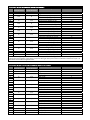
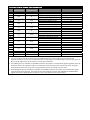
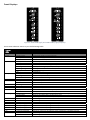
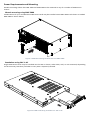
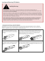
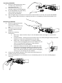
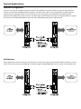
USER MANUAL Multi‐Standard Interface for Serial Data Communications FOM‐1090 / FOM‐1091 Warning for Your Protection 1. Read these instructions. 2. Keep these instructions. 3. Heed all warnings. 4. Follow all instructions. 5. Do not use this apparatus near water. 6. Clean only with a dry cloth. 7. Do not block any of the ventilation openings. Install in accordance with the manufacturer’s instructions. 8. Do not install near any heat sources such as radiators, heat registers, stoves, or other apparatus (including amplifiers) that produce heat. 9. Only use attachments/accessories specified by the manufacturer. 10. Unplug this apparatus during lightning storms or when unused for long periods of time. 11. Refer all servicing to qualified service personnel. Servicing is required when the apparatus has been damaged in any way, such as power‐supply cord or plug is damaged, liquid has been spilled or objects have fallen into the apparatus, the apparatus has been exposed to rain or moisture, does not operate normally, or has been dropped. The apparatus shall not be exposed to dripping or splashing. No objects filled with liquids, such as vases, shall be placed on the apparatus. “WARNING: To reduce the risk of fire or electric shock, do not expose this apparatus to rain or moisture.” General Installation Instructions Please consider these general instructions in addition to any product‐specific instructions in the “Installation” chapter of this manual. Unpacking Check the equipment for any transport damage. If the unit is mechanically damaged, if liquids have been spilled or if objects have fallen into the unit, it must not be connected to the AC power outlet, or it must be immediately disconnected by unplugging the power cable. Repair must only be performed by trained personnel in accordance with the applicable regulations. Installation Site Install the unit in a place where the following conditions are met: The temperature and the relative humidity of the operating environment must be within the specified limits during operation of the unit. Values specified are applicable to the air inlets of the unit. Condensation may not be present during operation. If the unit is installed in a location subject to large variations of ambient temperature (e.g. in an OB‐van), appropriate precautions must be taken. Unobstructed air flow is essential for proper operation. Ventilation openings of the unit are a functional part of the design and must not be obstructed in any way during operation (e.g. ‐ by objects placed upon them, placement of the unit on a soft surface, or improper installation of the unit within a rack or piece of furniture). The unit must not be unduly exposed to external heat sources (direct sunlight, spot lights). Ambient Temperature Units and systems by FiberPlex are generally designed for an ambient temperature range (i.e. temperature of the incoming air) of +5...+40 °C. When rack mounting the units, the following facts must be considered: The permissible ambient temperature range for operation of the semiconductor components is 0 °C to +70 °C (commercial temperature range for operation). The air flow through the installation must allow exhaust air to remain cooler than 70 °C at all times. Average temperature increase of the cooling air shall be about 20 C°, allowing for an additional maximum 10 C° increase at the hottest components. If the cooling function of the installation must be monitored (e.g. for fan failure or illumination with spot lamps), the exhaust air temperature must be measured directly above the modules at several places within the enclosure. Warranty, Service and Terms and Conditions of Sale For information about Warranty or Service information, please see our published ‘Terms and Conditions of Sale’. This document is available on fiberplex.com or can be obtained by requesting it from [email protected] or calling 301.604.0100. Disposal Disposal of Packing Materials The packing materials have been selected with environmental and disposal issues in mind. All packing material can be recycled. Recycling packing saves raw materials and reduces the volume of waste. If you need to dispose of the transport packing materials, recycling is encouraged. Disposal of Used Equipment Used equipment contains valuable raw materials as well as substances that must be disposed of professionally. Please dispose of used equipment via an authorized specialist dealer or via the public waste disposal system, ensuring any material that can be recycled has been. Please take care that your used equipment cannot be abused. After having disconnected your used equipment from the mains supply, make sure that the mains connector and the mains cable are made useless. Disclaimer The information in this document has been carefully checked and is believed to be accurate at the time of publication. However, no liability is assumed by FiberPlex for inaccuracies, errors, or omissions, nor for loss or damage resulting either directly or indirectly from use of the information contained herein. Introduction The FOM‐1090 and FOM‐1091 fiber optic isolator\modem cards provides for full synchronous, asynchronous, or isochronous interfacing to serial data communications equipment. The unit is transparent to all data formats and protocol, and supports timing from the DCE and DTE as well as uncommon clocking styles such as gapped clock or gated clocks that stop in different states to indicate status. The status and direction of all supported signals is shown on front panel indicators in addition to power supply and optical link status for each card. Key Features Supported Serial Interfaces: o TIA‐530 & TIA‐530A o TIA‐232 o TIA‐574, with adapter cable o TIA‐449, with adapter cable, using common subset of control signals o V.35, with adapter cable o X.21, with adapter cable Supported Electrical Standards: o TIA‐422/V.11/FED‐STD‐1030A o TIA‐423/V.10/FED‐STD‐1020A o TIA‐232/V.28 o V.35 o MIL‐STD‐100 o MIL‐STD‐188‐114A, Balanced types 1 and 2 (in V.11 mode) o MIL‐STD‐188‐114A, Unbalanced (in V.10 mode) o MIL‐STD‐188C (Limited compatibility – see section on Compatibility with MIL‐STD Circuits) Chassis Mounted for High Density Applications Differences between FOM‐1090 and FOM‐1091 The FOM‐1091 mates with and converts to DCE. The FOM‐1090 mates with and converts to DTE. Getting Started Initial Inspection Immediately upon receipt, inspect the shipping container for damage. The container should be retained until the shipment has been checked for completeness and the equipment has been checked mechanically and electrically. If the shipment is incomplete, if there is mechanical damage, or if the unit fails to operate notify FiberPlex and make the shipping materials available for the carrier's inspection. Rear Indicators/Connections Figure 1 FOM‐1090 (left) and FOM‐1091 (right) Rear Faces 1 Chassis Mounting Screws (x2) – These captive fasteners secure the FOM card in the chassis. The heads are knurled so that no tool is required for mounting/dismounting. 2 Optics Status LED – This LED, for each position, indicates status as per the following table; Optics Status LED Status Steady Green Flashing Green Steady Yellow Flashing Yellow Flashing Orange Steady Red Off Description Optics in sync at each end of link Local optical RX is receiving errors Remote optical RX loss of signal or sync Local optical RX signal present, but no sync Card type mismatch at remote end; the two cards are not compatible No optical RX signal Card failure 3 Status LED – This LED, for each position, indicates status as per the following table; Power Status LED Status Steady Green Steady Red Off Description Card power supply normal operation Card power supply failure or in over‐current protection Card failure or main power failure 5 DTE Connector & DCE Connector – Connect Data Terminal Equipment and Data Communications Equipment at these ports. The DTE is a female (sockets), D‐subminiature, 25‐position connector; the DCE is similar, but male (pins). Jackscrews are provided for securement. See pinout below. 4 Pinouts (TIA‐530, TIA‐530A [422]) Pin FOM‐1091 (DCE) Direction FOM‐1090 (DTE) Direction TIA‐530 Configuration TIA‐530A Configuration 1 Chassis Ground Chassis Ground 7 Signal Ground Signal Ground 2 Send Data A (SD) (V.11) Send Data A (SD) (V.11) Out In 14 Send Data B (SD\) (V.11) Send Data B (SD\) (V.11) 3 Receive Data A (RD) (V.11) Receive Data A (RD) (V.11) In Out 16 Receive Data B (RD\) (V.11) Receive Data B (RD\) (V.11) 4 Request To Send A (RTS) (V.11) Request To Send A (RTS) (V.11) Out In 19 Request To Send B (RTS\) (V.11) Request To Send B (RTS\) (V.11) 5 Clear To Send A (CTS) (V.11) Clear To Send A (CTS) (V.11) In Out 13 Clear To Send B (CTS\) (V.11) Clear To Send B (CTS\) (V.11) 20 Terminal Ready A (TR) (V.11) Terminal Ready (TR) (V.10) Out In 23 Terminal Ready B (TR\) (V.11) ‐ 6 Data Set Ready A (DSR) (V.11) Data Set Ready (DSR) (V.10) In Out 22 Data Set Ready B (DSR\) (V.11) Incoming Call (IC) (V.10) 24 Terminal Timing A (TT) (V.11) Terminal Timing A (TT) (V.11) Out In 11 Terminal Timing B (TT\) (V.11) Terminal Timing B (TT\) (V.11) 8 Receiver Ready A (RR) (V.11) Receiver Ready A (RR) (V.11) In Out 10 Receiver Ready B (RR\) (V.11) Receiver Ready B (RR\) (V.11) 15 Send Timing A (ST) (V.11) Send Timing A (ST) (V.11) In Out 12 Send Timing B (ST\) (V.11) Send Timing B (ST\) (V.11) 17 Receive Timing A (RT) (V.11) Receive Timing A (RT) (V.11) In Out 9 Receive Timing B (RT\) (V.11) Receive Timing B (RT\) (V.11) 18 Out In Local Loopback (LL) (V.10) Local Loopback (LL) (V.10) 25 In Out Test Mode (TM) (V.10) Test Mode (TM) (V.10) 21 Out In Remote Loopback (RL) (V.10) Remote Loopback (RL) (V.10) Note: On the TIA‐530A interface the DM and TR signals become single‐ended and the single‐ended signal IC is added. Pinouts (TIA‐449 with adapter cable information) Pin FOM‐1091 (DCE) Direction FOM‐1090 (DTE) Direction TIA‐449 Configuration DB‐37 Pin 1 Chassis Ground 1 7 Signal Ground 19, 20, 37 2 Send Data A (SD) (V.11) 4 Out In 14 Send Data B (SD\) (V.11) 22 3 Receive Data A (RD) (V.11) 6 In Out 16 Receive Data B (RD\) (V.11) 24 4 Request To Send A (RTS) (V.11) 7 Out In 19 Request To Send B (RTS\) (V.11) 25 5 Clear To Send A (CTS) (V.11) 9 In Out 13 Clear To Send B (CTS\) (V.11) 27 20 Terminal Ready A (TR) (V.11) 12 Out In 23 Terminal Ready B (TR\) (V.11) 30 6 Data Set Ready A (DSR) (V.11) 11 In Out 22 Data Set Ready B (DSR\) (V.11) 29 24 Terminal Timing A (TT) (V.11) 17 Out In 11 Terminal Timing B (TT\) (V.11) 35 8 Receiver Ready A (RR) (V.11) 13 In Out 10 Receiver Ready B (RR\) (V.11) 31 15 Send Timing A (ST) (V.11) 5 In Out 12 Send Timing B (ST\) (V.11) 23 17 Receive Timing A (RT) (V.11) 8 In Out 9 Receive Timing B (RT\) (V.11) 26 18 Out In Local Loopback (LL) (V.10) 10 25 In Out Test Mode (TM) (V.10) 18 21 Out In Remote Loopback (RL) (V.10) 14 Note: For best signal performance do not tie pin 20 (Receive Common), pin 37 (Send Common), or pin 19 (Signal Ground) together at the DB‐37 connector. Bring all three pins back on individual conductors to pin 7 of the DB‐25 and tie them together there. Pinouts (TIA‐232; TIA‐574 with adapter cable information) Pin 1 7 2 14 3 16 4 19 5 13 20 23 6 22 24 11 8 10 15 12 17 9 18 25 21 FOM‐1091 (DCE) Direction Out ‐ In ‐ Out ‐ In ‐ Out ‐ In In Out ‐ In ‐ In ‐ In ‐ Out In Out FOM‐1090 (DTE) Direction In ‐ Out ‐ In ‐ Out ‐ In ‐ Out Out In ‐ Out ‐ Out ‐ Out ‐ In Out In TIA‐232 Configuration Chassis Ground Signal Ground TD (V.28) ‐ RD (V.28) ‐ RTS/RS (V.28) ‐ CTS/CS (V.28) ‐ DTR/TR (V.28) ‐ DSR/DM (V.28) RI/IC (V.28) TT (V.28) ‐ DCD/RR (V.28) ‐ ST (V.28) ‐ RT (V.11) ‐ LL (V.28) TM (V.28) RL (V.28) TIA‐574 DB‐9 Pin ‐ 5 3 ‐ 2 ‐ 7 ‐ 8 ‐ 4 ‐ 6 9 ‐ ‐ 1 ‐ ‐ ‐ ‐ ‐ ‐ ‐ ‐ Pinouts (X.21 with adapter cable information) Pin FOM‐1091 (DCE) Direction FOM‐1090 (DTE) Direction X.21 Configuration DB‐15 Pin 1 Chassis Ground 1 7 Signal Ground 8 2 Send Data A (SD) (V.11) 2 Out In 14 Send Data B (SD\) (V.11) 9 3 Receive Data A (RD) (V.11) 4 In Out 16 Receive Data B (RD\) (V.11) 11 4 Request To Send A (RTS) (V.11) ‐ Out In 19 Request To Send B (RTS\) (V.11) ‐ 5 Clear To Send A (CTS) (V.11) ‐ In Out 13 Clear To Send B (CTS\) (V.11) ‐ 20 IND A (TR) (V.11) 3 Out In 23 IND B (TR\) (V.11) 10 6 DM A (V.11) ‐ In Out 22 DM B (V.11) ‐ 24 Terminal Timing A (TT) (V.11) ‐ Out In 11 Terminal Timing B (TT\) (V.11) ‐ 8 CON A (V.11) 5 In Out 10 CON B (V.11) 12 15 BT A (ST) (V.11) 7 In Out 12 BT B (V.11) 14 17 ST A (V.11) 6 In Out 9 ST B (V.11) 13 18 ‐ ‐ ‐ ‐ 25 ‐ ‐ ‐ ‐ 21 ‐ ‐ ‐ ‐ Notes: The X.21 ST signal will be routed through the FOM labeled as RT (pins 17 & 9) as this would be the equivalent clock for conversion to other interfaces. The BT signal is routed through on the ST signal (pins 15 & 12). The BT signal may not be present on some X.21 interfaces. The FOM signal TT is available on the DB25 connector, but there is no equivalent signal assigned to the X.21 interface. Some X.21 interfaces support a companion clock sourced from the same end as the TD signal, using the BT pins for that clock. The TT signal may be used for that clock in those cases. The FOM signals RS, CS, and DM are available on the DB25 connector, but there are no equivalent signals assigned to the X.21 interface. These signals may alternately be used for the CONTROL and INDICATION signals to allow for adapting flow control to a non‐X.21 interface at the opposite end. Pinouts (V.35 with adapter cable information) Pin 1 7 2 14 3 16 4 19 5 13 20 23 6 22 24 11 8 10 15 12 17 9 18 25 21 FOM‐1091 (DCE) Direction FOM‐1090 (DTE) Direction Out In In Out Out ‐ In ‐ Out ‐ In In In ‐ Out ‐ In ‐ Out Out Out In In ‐ Out ‐ In Out In Out Out In Out In Out In V.35 Chassis Ground Signal Ground TD A (V.35) TD B (V.35) RD A (V.35) RD B (V.35) RTS/RS (V.28) ‐ CTS/CS (V.28) ‐ DTR/TR (V.28) ‐ DSR/DM (V.28) RI/IC (V.28) TT A (V.35) TT B (V.35) DCD/RR (V.28) ‐ ST A (V.35) ST B (V.35) RT A (V.28) RT B (V.28) LL (V.28) TM (V.28) RL (V.28) M‐34 Pin A B P S R T C ‐ D ‐ H ‐ E J U W F ‐ Y AA V X L NN N 6 Interface Status LED – This LED will flash a fixed number of times indicating the selected interface mode. It will be yellow for a DCE unit and orange for a DTE. It will be solid red for a disabled interface (See section “DIP Switch Settings”, subsection “Configuring DIP Switch Parameters” for more information). 7 Optical Fiber Connections – This position may be a pair of ST connectors, LC connectors or an SFP slot, if so ordered. SFP MSA Compliance The SFP Multisource Agreement (MSA) is an agreement that was drafted among competing manufacturers of SFP optical modules. The SFF Committee was formed to oversee the creation and maintenance of these agreements including the SFP MSA designated as INF‐8074i. This agreement describes a mutually agreed upon standard for the form and function of SFP modules. However, not all SFPs produced are MSA compliant. The MSA provides for a transceiver (TX/RX) pinout. Other industries such as broadcast had the need for dual TX and dual RX SFP for uni‐directional applications such as video. Naturally, a non‐MSA standard was introduced allocating pinout assignments for dual output and dual input I/O configurations. In addition, the some of the internal serial communication pins were reassigned. The FOM‐1090/1091 will only accept MSA compliant SFP Modules. Front Displays Figure 2 FOM‐1090 (left) and FOM‐1091 (right) Displays These LEDs indicates status as per the following table Display LEDs Label Status Description Power Steady Green Steady Red Off Steady Green Flashing Green Steady Yellow Flashing Yellow Flashing Orange Steady Red Off Steady Green Flashing Red Off Flashing Steady Off Flashing Steady Off Steady Green Off Steady Green Flashing Red Off Steady Off Yellow/Orange/Red Yellow/Orange/Red Yellow/Orange/Red Yellow/Orange/Red Yellow/Orange/Red Yellow/Orange/Red Steady Off Card power supply normal operation Card power supply failure or in over‐current protection Card failure or main power failure Optics in sync at each end of link Local optical RX is receiving errors Remote optical RX loss of signal or sync Local optical RX signal present, but no sync Card type mismatch at remote end; the two cards are not compatible No optical RX signal Card failure Optional switch setting is in use Card is in Loop Back mode No optional switch setting is in use; text is turned off Data transitions detected Data in steady SPACE condition Data in steady MARK condition Clock transitions detected Clock in steady On state Clock in steady Off state Optional data invert in use – typically used for MIL interfaces No optional data invert – normal operation; text is turned off Optional TD signal regeneration in use – FOM‐1091 only Optional TD regeneration configuration error No TD regeneration – normal operation; text is turned off Control signal in On state Control signal in Off state Yellow for a DCE unit, Orange for a DTE; solid Red is a disabled interface Yellow for a DCE unit, Orange for a DTE; solid Red is a disabled interface Yellow for a DCE unit, Orange for a DTE; solid Red is a disabled interface Yellow for a DCE unit, Orange for a DTE; solid Red is a disabled interface Yellow for a DCE unit, Orange for a DTE; solid Red is a disabled interface Yellow for a DCE unit, Orange for a DTE; solid Red is a disabled interface Control signal in On state Control signal in Off state Optics SW Option TD RD TT RT ST Data Invert Data Regen RS CS TR DM RR LL RL TM IC Power Requirements and Mounting Flexible mounting allows the FOM‐1090 and FOM‐1091 to be mounted in any of a number of FOM‐series chassis. Chassis mounting using RMC‐5000 Combinations of up to 16 FiberPlex FOM‐series cards may be installed into a RMC‐5000 rack chassis. A loaded RMC‐5000 is shown below; Figure 3 FOM Card being installed into an RMC‐5000 Standalone using SAC‐1‐AC Single FOM‐series cards may be installed into the SAC‐1 chassis, either desk, wall, or rack mounted, depending on the accessory brackets (included in every SAC‐1 shipment) utilized. Figure 4 FOM Card being installed in a SAC‐1‐AC Inserting and Removing SFP Modules Handling Warnings SFP Modules are static sensitive. To prevent damage from electrostatic discharge (ESD), it is recommended to attach an ESD preventative wrist strap to your wrist and to a bare metal surface when you install or remove an SFP Module. Disconnect all optical or copper cables from SFP Modules prior to installing or removing the SFP Module. Failure to do so could result in damage to the cable, cable connector or the SFP Module itself. Removing and inserting an SFP Module can shorten its useful life, so you should not remove and insert SFP Modules any more often than is absolutely necessary. Protect optical SFP modules by inserting clean dust covers into them after the cables are removed. Be sure to clean the optic surfaces of the fiber cables before you plug them back into the optical ports of another SFP module. Avoid getting dust and other contaminants into the optical ports of your SFP modules, because the optics will not work correctly when obstructed with dust. Identify the Latch Type of the SFP Module SFP Modules have various latching mechanisms to secure them into the SFP Cage of a device. FiberPlex Modules can support a host of manufacturers and brands of SFP Modules so the user may encounter any number of different latches. Some of these are described below. Bail Clasp Actuator Button The bail clasp SFP module has a clasp that you use to remove or install the SFP module. The actuator button SFP module includes a button that you push in order to remove the SFP module from a port. This button can either lift ‘Up’ or press ‘In’ to release the SFP Module depending on the manufacturer. Mylar Tab Slide Tab The Mylar tab SFP module has a tab that you pull to remove the module from a port. The slide tab SFP module has a tab underneath the front of the SFP module that you use to disengage the module from a port. Inserting a Module 1) 2) 3) 4) Attach an ESD‐preventative wrist or ankle strap, following its instructions for use. Disconnect and remove all interface cables from SFP Module. If the SFP Module has a Bail Clasp , close the Bail Clasp before inserting the SFP Module. With the gold finger connector on the bottom and the label on the top, line up the SFP Module with the empty cage and slide it in making sure that it is completely inserted and seated in the cage. Removing a Module 1) 2) 3) 4) 5) Attach an ESD‐preventative wrist or ankle strap, following its instructions for use. Disconnect and remove all interface cables from SFP Module. Release the latching mechanism. Bail Clasp – Open the bail clasp on the SFP Module with your finger in a downward direction. Actuator Button – Gently press the actuator up (or in) while pulling the body of the SFP Module to release the SFP Module from the cage. Mylar Tab – Pull the tab gently in a straight outward motion until it disengages from the port. Make sure the tab is not twisted when pulling as it may become disconnected from the SFP Module. Slide Tab ‐ With your thumb, push the slide tab on the bottom front of the SFP module in the direction of the equipment to disengage the module from the line card port. If you pull on the SFP module without disengaging the tab, you can damage the SFP module. Grasp the SFP Module between your thumb and index finger and carefully remove it from the port Place the SFP Module on an antistatic mat, or immediately place it in a static shielding bag or container DIP Switch Settings Compatibility with MIL‐STD circuits The drivers and receivers for V.11 signals are compatible with the MIL‐STD balanced specifications and the V.10 interface is similar to MIL‐STD unbalanced. MIL‐STD‐100 signals use the same negative MARK condition as TIA circuits, so there is no need to invert the TD and RD signals. MIL‐STD‐188‐114A is set‐up for user control of the MARK level, so the need for data inversion at the FOM will need to be made on a case‐by‐case basis. If the MIL‐STD interface uses any unbalanced signals, such as MIL‐STD‐188C (note that this standard uses a positive MARK), then provisions will need to be made to externally bias one side of the receivers on the FOM to use them single‐ended. Note that the MIL standards are only an electrical specification and do not specify a pin out or connector type, so a custom cable will be required in many cases. Asynchronous, Isochronous, or Synchronous operation The FOM is transparent to data and clocking formats, so there are no switch settings for distinguishing the different modes of operation. When a pair of FOM‐1090 units is used as modem link between two DTEs, all of the input signals are transferred to the crossed‐over corresponding outputs (i.e. ‐ TT from the DTE is provided as RT out of the FOM‐1090) at the opposite end. When the FOM is used in Send Timing applications, certain switch options may be used to eliminate clocking issues that may arise. Those options are explained below. Send Data Regeneration when using Send Timing from the DCE The typical Send Timing set‐up has the DCE supplying all clocks. The ST signal is generated at the DCE and then carried to the remote DTE. In return, the remote DTE then clocks the Send Data out of itself on the rising edge of the supplied ST signal. The Send Data is carried back to the DCE where it is clocked in, sampling the data bit on the falling edge of the generated ST clock. Alignment problems arise due to propagation delay when certain combinations of data rate and cable distance (both copper and fiber) result in the Send Data transitions occurring near the falling edge of the ST signal at the DCE. As an example, using a rough number of 4 ns delay per meter of cable, 25 meters of cable with a 2.5 mHz clock will cause a 180 degree shift in the ST‐SD relationship at the DCE interface. (There is actually 50 meters of propagation delay since the clock travels 25 meters in one direction and the data travels 25 meters in the other). This is without taking into account the delays of the line drivers and receivers in the DTE. The FOM‐1091 regeneration options make up for this in two ways. The first is to correct for any SD‐ST misalignment due to propagation delay from the FOM‐1091 to the DCE by delaying the SD signal out of the FOM by one half of a ST clock cycle. The second is the FOM has the ability to retime the incoming SD data internally with the incoming ST signal, which removes any sampling jitter from the SD signal as well as correcting for propagation delays. While the falling edge of the ST signal from the DCE is ideally located mid‐bit of the SD signal coming into the DCE, it is not necessary for it to be mid‐bit. In fact, it’s usually not mid‐bit due to delays. This is often misunderstood. The actual requirement is that the set‐up time for the register that the SD signal is being loaded into be met and this is usually a fraction of the available bit time. The only time there is a problem is when the falling edge of the ST is too close to the SD transitions at the DCE interface and this prevents the set‐ up time from being met. If the ST falling edge is far enough away from the SD transition edges (when the new SD data bit has met the set‐up time), the DCE will still clock the data reliably even though it isn’t mid‐bit. This is why many ST timing set‐ups will work with no regeneration required at all. When the edges are too close at the DCE the FOM will need to retime the data on the opposite edge of the ST signal by setting switch 1.8 to ON. This will allow that when the propagation delays are taken into account the edges have skewed enough to meet the set‐up time at the DCE. Note that in installations where the data rate may be changed or the cable lengths may change due to patch panel routing of equipment, it’s entirely possible that a combination of switch settings that works in one scenario will not work in another. The only solution to these situations is to insert more delay in one or more of the configurations by adding to cable length until all of the scenarios will work with the same switch settings. Setting the switches for using ST from the DCE Taking into account the variables of cable length from the DCE to the FOM‐1091, fiber cable length, cable length from the FOM‐1090 to the DTE, plus data rates, there is no single ‘correct’ setting for the ST invert and SD data regeneration switches. To correctly configure a synchronous link using Send Timing from the DCE, try one of the following: Correct for propagation delay between FOM‐1091 and DCE Determine if the removal of sampling jitter (it’s actually duty cycle distortion, not speed fluctuation) from the SD signal is desired. If it is, then proceed to next section below. If it is not a requirement, start with switches 1.6, 1.7, and 1.8 OFF. If the link functions properly, no regeneration configuration is needed. If the link does not operate properly, try accounting for propagation delay between the FOM‐1091 and the DCE by setting switch 1.8 to ON. The link should now operate correctly. If it does not, check cabling for the selected interface. If the link is running near its maximum speed it may be necessary to remove the sampling jitter from the SD signal as described in the next section. Regenerate Send Data signal and correct for propagation delay between FOM‐1091 and DCE If removal of sampling jitter is desired, set switch 1.6 ON and switches 1.7 and 1.8 OFF. This will allow the FOM to try to configure the regeneration settings on its’ own. If the link functions properly, no further regeneration configuration is needed. If the link does not operate properly, try accounting for propagation delay between the FOM‐1091 and the DCE by setting switch 1.8 to ON. If the above setting does not work, you will need to set the regeneration manually. Set switches 1.6 and 1.8 to OFF and set switch 1.7 to ON. If the link functions properly, no further regeneration configuration is needed. If the link still does not operate properly, again try accounting for propagation delay between the FOM‐1091 and the DCE by setting switch 1.8 to ON. If there are still errors, set switch 1.8 OFF and switch 1.6 to ON. If there are still errors, once again try accounting for propagation delay between the FOM‐1091 and the DCE by setting switch 1.8 to ON. One of the above groups of switch settings should allow a properly configured ST link to pass regenerated data to the DCE. The above is summarized in the following table. If calculating delays, keep in mind that the FOM card may introduce up to 40ns of I/O chipset and multiplexing delay itself. Switch 1.6 Switch 1.7 Switch 1.8 Note Off Off Off On Off Off On Off On Off On Off Off On On On On Off On On On Off Off Off No regeneration Auto Regeneration; data from FOM‐1091 transitions on rising edge of ST from DCE Auto Regeneration; data from FOM‐1091 transitions on falling edge of ST from DCE Manual Regeneration using rising edge of ST; data to DCE transitions on rising edge of ST from DCE Manual Regeneration using rising edge of ST; data to DCE transitions on falling edge of ST from DCE Manual Regeneration using failing edge of ST; data to DCE transitions on rising edge of ST from DCE Manual Regeneration using falling edge of ST; data to DCE transitions on falling edge of ST from DCE This setting has no effect on FOM‐1091 Switch Designations As shown below, each DIP switch is assigned a numerical designation which is keyed to the descriptive text; Figure 5 FOM‐1090, FOM‐1091 Switch Settings Configuring DIP Switch Parameters (All default settings are OFF with exception of interface selection.) Switch 1 Switches 1.1, 1.2, and 1.3: Interface Configuration (The rear panel INTF led will indicate the current interface setting.) Interface Switch 1.1 Switch 1.2 Switch 1.3 INTF LED X.21 Off On On 1 Flash TIA‐232 On On Off 2 Flashes V.35 On Off Off 3 Flashes TIA‐449 On Off On 4 Flashes TIA‐530 (422) Off On Off 5 Flashes Default (TIA‐530) Off Off Off TIA‐530A Off Off On 6 Flashes Disabled On On On Solid Red Switch 1.4: No Function Switch 1.5: Data Invert Changes the MARK condition for use with MIL‐STD type interfaces. The idle state for some MIL‐STD interfaces is the opposite of TIA and this setting allows the conversion from those MIL signals to TIA or between opposite state MIL interfaces when this switch is ON. Off Negative MARK On Positive MARK Switch 1.6: Data Regeneration A (FOM‐1091 ONLY) Enables FOM‐1091 auto or manual adjustment for regeneration of TD signal to DCE Off Normal operation On Enables various modes of TD out signal regeneration using ST signal from DCE in conjunction with switch 1.7. Switch 1.7: Data Regeneration B (FOM‐1091 ONLY) Enables FOM‐1091 auto or manual adjustment for regeneration of TD signal to DCE. Off Normal operation On Enables various modes of TD out signal regeneration using ST signal from DCE in conjunction with switch 1.6. Switch 1.8: Invert Send Timing Out (FOM‐1090 only) Inverts ST signal out of FOM‐1090. Off No inversion On ST out is inverted Switch 1.8: Data Regeneration C (FOM‐1091 only) Changes TD out relationship to ST in at FOM‐1091 when using Data Regeneration Switch. No function if Switch 1.6 and Switch 1.7 are off Off TD out transitions on rising edge of ST in On TD out transitions on falling edge of ST in Switch 2 Switch 2.1: Loop RS and CS locally This setting creates a loop back for the RS \ CS signals at the local end. The corresponding signal input is still carried across the link to the remote interface. The signal from the remote end is ignored. Off Normal RS and CS signal operation On On FOM‐1090: Loops RS input to CS output. CS signal from remote end is ignored. On FOM‐1091: Loops CS input to RS output. RS signal from remote end is ignored. Switch 2.2: Force RS / CS On Forces the corresponding output ON when unit is in optical sync. This overrides any signal from the far end of the link. Off Normal RS / CS operation On Forces RS out ON (FOM‐1091) or CS out ON (FOM‐1090) when unit is in optical sync. Switch 2.3: Loop TR and DM locally This setting creates a loop back for the TR / DM signals at the local end. The corresponding signal input is still carried across the link to the remote interface. The signal from the remote end is ignored. Off Normal TR and DM signal operation On On FOM‐1090: Loops TR input to DM output. DM signal from remote end is ignored. On FOM‐1091: Loops DM input to TR output. TR signal from remote end is ignored. Switch 2.4: Force TR / DM On Forces the corresponding output ON when unit is in optical sync. This overrides any signal from the far end of the link. Off Normal TR / DM operation On Forces TR out ON (FOM‐1091) or DM out ON (FOM‐1090) when unit is in optical sync. Switch 2.5: Force RR On (FOM‐1090 only; no function on FOM‐1091) Forces RR out ON when unit is in optical sync. This overrides RR from the far end of the link. Off Normal RR operation On Forces RR out ON (FOM‐1090) when unit is in optical sync. Switch 2.6: No Function Switch 2.7: No Line Terminations This switch removes all line terminations from the interface allowing the FOM to be used as a monitor point on an electrical link. The unit cannot selectively remove terminations on active lines; either all terminations are present or all are removed. Off Standard terminations for selected interface type are present On Terminations removed (Hi‐Z impedance) Switch 2.8: Loop Back Test Loops optic TX to optic RX and loops all copper signals to their corresponding signal (TD‐RD, TT‐RT, RS‐CS, TR‐DM, RL‐ TM, RR On, IC Off, LL Off) Off Normal operation On Loop back test Switch 3 Switch 3.1: No Function Switch 3.2: No Function Switch 3.3: Crypto to Crypto Null Modem (FOM‐1090 only; no function on FOM‐1091) This setting, when used with a FOM‐1090 at each end, reconfigures the interface to allow the fiber link to act as a null modem between two crypto units. The FOM‐1090 can be connected directly to the crypto using a standard straight‐ through 25 pin cable at each end, eliminating the need for a custom crossover cable. This configuration functions in TIA‐ 530, TIA‐530A, or TIA‐232 mode with a straight‐through cable or in TIA‐449 mode with a DB‐25 to DB‐37 adapter cable. When this switch is on it overrides configuration switches 2.1‐2.5. Off Normal operation On Crypto crossover mode (no function on FOM‐1091) Switch 3.4: No Function Switch 3.5: No Function Switch 3.6: No Function Switch 3.7: No Function Switch 3.8: Display Test This setting will cause the front panel display to flash each of the indicators yellow or orange (with the exception of the power led, which remains green) for verification purposes. The rear OPT led will also flash. The unit continues to function normally ‐ only the display is affected. Off Normal indicator operation On All indictors except power will flash. The Optics led flashes out of phase with the others. Typical Applications Standard Configuration The user can achieve complete electrical isolation for NRZ data communications in areas of high electrical noise or in/out of RF shielded enclosures (SCIF). The fiber optic cable is not susceptible to induced impulse noise and since signal ground is not carried over the link, the signal is not affected by elevated ground potential from lightning or other sources. The fiber optic cable enhances privacy of communications. A typical link consists of a FOM‐1090 (DCE) at one end and a FOM‐1091 (DTE) at the opposite end. Null Modem Some applications, due to cabling or infrastructure constraints require a Null modem between devices. A pair of the same units may be used together as when using two FOM‐1090 DCE units to create a null modem link. Interface Conversion A different interface may be selected at each end allowing the user to create a fiber link between two electrically incompatible interfaces without requiring a separate interface converter. Simply set each unit to the desired electrical interface and the conversion will happen automatically. Be sure to look carefully at the pinout diagrams to know exactly what to anticipate in your cabling. Crypto to Crypto Null Modem A unique application is a crypto to crypto null modem, however a standard null modem cable does not work due to specific clocking requirements. The FOM‐1090 has the capability to re‐route timing and controls allowing this crypto to crypto operation while using standard straight‐through cables. Specifications Figure 6 FOM‐1090 and FOM‐1091 Dimensions ELECTRICAL SPECIFICATIONS Power Requirement Max 34 ‐ ‐ Max ±6 ±7 ‐ 25 250 ‐ Max ±6 ±7 ‐ 250 ‐ Max ±15 ±15 ‐ 125 125 7 Max ±0.66 ±4 ‐ 20 110 Max ±15 ±15 ‐ 125 7 ‐ 85 50 Unit V mA ns Unit V V V MHz KHz Ω Unit V V V KHz KΩ Unit V V V KHz KHz KΩ Unit V V V MHz Ω Unit V V V KHz KΩ Ω °C °C Max Distance λ Bandwidth (km) (nm) (dB) T10 Multimode OM2 ST 0.4 850 12.5 L10 Multimode OM2 LC 0.4 850 14.5 T5A Singlemode OS1, OS2 ST 10 1310 14 L5A Singlemode OS1, OS2 LC 10 1310 12.75 C SFP Cage with no Optical Module Installed External SFP Interface Min Typ Max Data Rate ‐ 1.25 ‐ Recommended Jitter ‐ 40 ‐ Operating Voltage ‐ 3.3 Maximum Current ‐ ‐ 500 Optical Modules SFP MSA (SFF‐8431, SFF‐8432, SFF‐8433) compliant slot, data rate 1.25 Gbps Loss (dB) 5.7 5.7 8.5 8.5 Voltage Range Supply Current Sample Jitter TIA‐422 / V.11 / FED‐STD‐1030A Signals Output Levels into 100Ω Load Input Levels Input Threshold Maximum Speed, Data and Clock Lines Maximum Speed, Control Lines Input Termination (4KΩ min ‐ no termination) TIA‐423 / V.10 / FED‐STD‐1020A Signals Output Levels Open Circuit Input Levels Input Threshold Maximum Speed Input Termination TIA‐232 / V.28 Signals Output Levels into 3KΩ Termination Input Levels Input Threshold Maximum Speed, Data and Clock Lines Maximum Speed, Control Lines Input Termination Output Levels Open Circuit Input Levels Input Threshold Maximum Speed Input Termination V.35 Signals Output Levels into 3KΩ Termination Input Levels Input Threshold Maximum Speed Input Termination Receiver Off Impedance Storage Temperature Operating Temperature FOM‐1090 FOM‐1091 V.28 Signals Environmental Interface Connector Min Typ 20 24 ‐ 400 ‐ 8 Min Typ ±2 ‐ 0 ‐ ±0.2 ‐ 0 ‐ 0 ‐ ‐ 100 Min Typ ±4 ‐ 0 ‐ ±0.2 ‐ 0 ‐ 4 15 Min Typ ±5 ‐ 0 ‐ ±3 ‐ 0 ‐ 0 ‐ 3 ‐ Min Typ ±0.44 ‐ 0 ‐ ±0.2 ‐ 0 ‐ 90 ‐ Min Typ ±5 ‐ 0 ‐ ±3 ‐ 0 ‐ 3 ‐ 300 ‐ ‐40 ‐ 0 ‐ DB‐25 Female DB‐25 Male OPTICAL SPECIFICATIONS Order Suffix Fiber Fiber Type Connector Unit Gbps Psec VDC mA PHYSICAL SPECIFICATIONS Case Dimensions FOM‐1090 and FOM‐1091 Length 12.0 in (305 mm) Width 0.80 in (20 mm) Height 5.22 in (133 mm) Weight 0.5 lb (0.23 kg) UMFM1090 150205 18040-412 Guilford Rd. • Annapolis Junction, MD 20701 fiberplex.com • [email protected] • 301.604.0100