1
Rabbit® 4000 Microprocessor
User’s Manual
019–0152 •
070720–H
Rabbit 4000 Microprocessor User’s Manual
Part Number 019-0152 • 070720–H • Printed in U.S.A.
©2006–2007 Rabbit Semiconductor Inc. • All rights reserved.
No part of the contents of this manual may be reproduced or transmitted in any form or by any means
without the express written permission of Rabbit Semiconductor.
Permission is granted to make one or more copies as long as the copyright page contained therein is
included. These copies of the manuals may not be let or sold for any reason without the express written
permission of Rabbit Semiconductor.
Rabbit Semiconductor reserves the right to make changes and
improvements to its products without providing notice.
Trademarks
Rabbit and Dynamic C are registered trademarks of Rabbit Semiconductor Inc.
Rabbit 4000 is a trademark of Rabbit Semiconductor Inc.
The latest revision of this manual is available on the Rabbit Semiconductor Web site,
www.rabbit.com, for free, unregistered download.
Rabbit Semiconductor Inc.
www.rabbit.com
Rabbit 4000 Microprocessor User’s Manual
TABLE OF CONTENTS
Chapter 1. The Rabbit 4000 Processor
1.1
1.2
1.3
1.4
1.5
1
Introduction...........................................................................................................................................1
Features .................................................................................................................................................1
Block Diagram ......................................................................................................................................4
Basic Specifications ..............................................................................................................................5
Comparing Rabbit Microprocessors .....................................................................................................6
Chapter 2. Clocks
9
2.1 Overview...............................................................................................................................................9
2.1.1 Block Diagram ...........................................................................................................................10
2.1.2 Registers .....................................................................................................................................10
2.2 Dependencies ......................................................................................................................................11
2.2.1 I/O Pins ......................................................................................................................................11
2.2.2 Other Registers ...........................................................................................................................11
2.3 Operation ............................................................................................................................................12
2.3.1 Main Clock .................................................................................................................................12
2.3.2 Spectrum Spreader .....................................................................................................................13
2.3.3 Clock Doubler ............................................................................................................................15
2.3.4 32 kHz Clock .............................................................................................................................18
2.4 Register Descriptions ..........................................................................................................................20
Chapter 3. Reset and Bootstrap
25
3.1 Overview.............................................................................................................................................25
3.1.1 Block Diagram ...........................................................................................................................25
3.1.2 Registers .....................................................................................................................................26
3.2 Dependencies ......................................................................................................................................26
3.2.1 I/O Pins ......................................................................................................................................26
3.2.2 Clocks .........................................................................................................................................26
3.2.3 Other Registers ...........................................................................................................................26
3.2.4 Interrupts ....................................................................................................................................26
3.3 Operation ............................................................................................................................................27
3.4 Register Descriptions ..........................................................................................................................29
Chapter 4. System Management
31
4.1 Overview.............................................................................................................................................31
4.1.1 Block Diagram ...........................................................................................................................32
4.1.2 Registers .....................................................................................................................................32
4.2 Dependencies ......................................................................................................................................33
4.2.1 I/O Pins ......................................................................................................................................33
4.2.2 Clocks .........................................................................................................................................33
4.2.3 Interrupts ....................................................................................................................................33
4.3 Operation ............................................................................................................................................34
4.3.1 Periodic Interrupt .......................................................................................................................34
4.3.2 Real-Time Clock ........................................................................................................................34
4.3.3 Watchdog Timer ........................................................................................................................35
4.3.4 Secondary Watchdog Timer .......................................................................................................35
4.4 Register Descriptions ..........................................................................................................................36
Table of Contents
Chapter 5. Memory Management
41
5.1 Overview ............................................................................................................................................ 41
5.1.1 Block Diagram ........................................................................................................................... 43
5.1.2 Registers .................................................................................................................................... 44
5.2 Dependencies ..................................................................................................................................... 45
5.2.1 I/O Pins ...................................................................................................................................... 45
5.2.2 Clocks ........................................................................................................................................ 45
5.2.3 Other Registers .......................................................................................................................... 45
5.2.4 Interrupts .................................................................................................................................... 45
5.3 Operation ............................................................................................................................................ 46
5.3.1 Memory Management Unit (MMU) .......................................................................................... 46
5.3.2 8-bit Operation ........................................................................................................................... 47
5.3.3 16-bit and Page Modes .............................................................................................................. 49
5.3.4 Separate Instruction and Data Space ......................................................................................... 52
5.3.5 Memory Protection .................................................................................................................... 52
5.3.6 Stack Protection ......................................................................................................................... 52
5.4 Register Descriptions ......................................................................................................................... 53
Chapter 6. Interrupts
65
6.1 Overview ............................................................................................................................................ 65
6.2 Operation ............................................................................................................................................ 66
6.3 Interrupt Tables .................................................................................................................................. 66
Chapter 7. External Interrupts
69
7.1 Overview ............................................................................................................................................ 69
7.2 Block Diagram ................................................................................................................................... 69
7.2.1 Registers .................................................................................................................................... 70
7.3 Dependencies ..................................................................................................................................... 70
7.3.1 I/O Pins ...................................................................................................................................... 70
7.3.2 Clocks ........................................................................................................................................ 70
7.3.3 Interrupts .................................................................................................................................... 70
7.4 Operation ............................................................................................................................................ 70
7.4.1 Example ISR .............................................................................................................................. 70
7.5 Register Descriptions ......................................................................................................................... 71
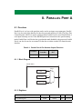
Chapter 8. Parallel Port A
73
8.1 Overview ............................................................................................................................................ 73
8.1.1 Block Diagram ........................................................................................................................... 73
8.1.2 Registers .................................................................................................................................... 73
8.2 Dependencies ..................................................................................................................................... 74
8.2.1 I/O Pins ...................................................................................................................................... 74
8.2.2 Clocks ........................................................................................................................................ 74
8.2.3 Other Registers .......................................................................................................................... 74
8.2.4 Interrupts .................................................................................................................................... 74
8.3 Operation ............................................................................................................................................ 74
8.4 Register Descriptions ......................................................................................................................... 75
Chapter 9. Parallel Port B
77
9.1 Overview ............................................................................................................................................ 77
9.1.1 Block Diagram ........................................................................................................................... 78
9.1.2 Registers .................................................................................................................................... 78
9.2 Dependencies ..................................................................................................................................... 78
9.2.1 I/O Pins ...................................................................................................................................... 78
9.2.2 Clocks ........................................................................................................................................ 78
9.2.3 Other Registers .......................................................................................................................... 78
9.2.4 Interrupts .................................................................................................................................... 79
9.3 Operation ............................................................................................................................................ 79
9.4 Register Descriptions ......................................................................................................................... 79
Rabbit 4000 Microprocessor User’s Manual
Chapter 10. Parallel Port C
81
10.1 Overview...........................................................................................................................................81
10.1.1 Block Diagram .........................................................................................................................82
10.1.2 Registers ...................................................................................................................................82
10.2 Dependencies ....................................................................................................................................83
10.2.1 I/O Pins ....................................................................................................................................83
10.2.2 Clocks .......................................................................................................................................83
10.2.3 Other Registers .........................................................................................................................83
10.2.4 Interrupts ..................................................................................................................................83
10.3 Operation ..........................................................................................................................................83
10.4 Register Descriptions ........................................................................................................................84
Chapter 11. Parallel Port D
87
11.1 Overview...........................................................................................................................................87
11.1.1 Block Diagram .........................................................................................................................89
11.1.2 Registers ...................................................................................................................................90
11.2 Dependencies ....................................................................................................................................90
11.2.1 I/O Pins ....................................................................................................................................90
11.2.2 Clocks .......................................................................................................................................90
11.2.3 Other Registers .........................................................................................................................91
11.2.4 Interrupts ..................................................................................................................................91
11.3 Operation ..........................................................................................................................................91
11.4 Register Descriptions ........................................................................................................................92
Chapter 12. Parallel Port E
97
12.1 Overview...........................................................................................................................................97
12.1.1 Block Diagram .........................................................................................................................99
12.1.2 Registers .................................................................................................................................100
12.2 Dependencies ..................................................................................................................................100
12.2.1 I/O Pins ..................................................................................................................................100
12.2.2 Clocks .....................................................................................................................................100
12.2.3 Other Registers .......................................................................................................................101
12.2.4 Interrupts ................................................................................................................................101
12.3 Operation ........................................................................................................................................101
12.4 Register Descriptions ......................................................................................................................102
Chapter 13. Timer A
107
13.1 Overview.........................................................................................................................................107
13.1.1 Block Diagram .......................................................................................................................109
13.1.2 Registers .................................................................................................................................110
13.2 Dependencies ..................................................................................................................................110
13.2.1 I/O Pins ..................................................................................................................................110
13.2.2 Clocks .....................................................................................................................................110
13.2.3 Other Registers .......................................................................................................................110
13.2.4 Interrupts ................................................................................................................................111
13.3 Operation ........................................................................................................................................111
13.3.1 Handling Interrupts ................................................................................................................111
13.3.2 Example ISR ..........................................................................................................................111
13.4 Register Descriptions ......................................................................................................................112
Chapter 14. Timer B
115
14.1 Overview.........................................................................................................................................115
14.1.1 Block Diagram .......................................................................................................................115
14.1.2 Registers .................................................................................................................................116
14.2 Dependencies ..................................................................................................................................116
14.2.1 I/O Pins ..................................................................................................................................116
14.2.2 Clocks .....................................................................................................................................116
14.2.3 Other Registers .......................................................................................................................116
14.2.4 Interrupts ................................................................................................................................116
Table of Contents
14.3 Operation........................................................................................................................................ 117
14.3.1 Handling Interrupts ................................................................................................................ 117
14.3.2 Example ISR .......................................................................................................................... 117
14.4 Register Descriptions ..................................................................................................................... 118
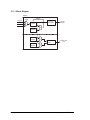
Chapter 15. Timer C
121
15.1 Overview ........................................................................................................................................ 121
15.1.1 Block Diagram ....................................................................................................................... 122
15.1.2 Registers ................................................................................................................................ 123
15.2 Dependencies ................................................................................................................................. 124
15.2.1 I/O Pins .................................................................................................................................. 124
15.2.2 Clocks .................................................................................................................................... 124
15.2.3 Other Registers ...................................................................................................................... 124
15.2.4 Interrupts ................................................................................................................................ 124
15.3 Operation........................................................................................................................................ 125
15.3.1 Handling Interrupts ................................................................................................................ 125
15.3.2 Example ISR .......................................................................................................................... 125
15.4 Register Descriptions ..................................................................................................................... 126
Chapter 16. Serial Ports A – D
129
16.1 Overview ........................................................................................................................................ 129
16.1.1 Block Diagram ....................................................................................................................... 131
16.1.2 Registers ................................................................................................................................ 132
16.2 Dependencies ................................................................................................................................. 133
16.2.1 I/O Pins .................................................................................................................................. 133
16.2.2 Clocks .................................................................................................................................... 134
16.2.3 Other Registers ...................................................................................................................... 134
16.2.4 Interrupts ................................................................................................................................ 134
16.3 Operation........................................................................................................................................ 135
16.3.1 Asynchronous Mode .............................................................................................................. 135
16.3.2 Clocked Serial Mode ............................................................................................................. 136
16.4 Register Descriptions ..................................................................................................................... 138
Chapter 17. Serial Ports E – F
145
17.1 Overview ........................................................................................................................................ 145
17.1.1 Block Diagram ....................................................................................................................... 146
17.1.2 Registers ................................................................................................................................ 147
17.2 Dependencies ................................................................................................................................. 148
17.2.1 I/O Pins .................................................................................................................................. 148
17.2.2 Clocks .................................................................................................................................... 148
17.2.3 Other Registers ...................................................................................................................... 148
17.2.4 Interrupts ................................................................................................................................ 149
17.3 Operation........................................................................................................................................ 150
17.3.1 Asynchronous Mode .............................................................................................................. 150
17.3.2 HDLC Mode .......................................................................................................................... 150
17.3.3 More on Clock Synchronization and Data Encoding ............................................................ 151
17.4 Register Descriptions ..................................................................................................................... 155
Chapter 18. Slave Port
161
18.1 Overview ........................................................................................................................................ 161
18.1.1 Block Diagram ....................................................................................................................... 162
18.1.2 Registers ................................................................................................................................ 162
18.2 Dependencies ................................................................................................................................. 163
18.2.1 I/O Pins .................................................................................................................................. 163
18.2.2 Clocks .................................................................................................................................... 163
18.2.3 Interrupts ................................................................................................................................ 163
Rabbit 4000 Microprocessor User’s Manual
18.3 Operation ........................................................................................................................................164
18.3.1 Master Setup ..........................................................................................................................165
18.3.2 Slave Setup .............................................................................................................................165
18.3.3 Master/Slave Communication ................................................................................................166
18.3.4 Slave/Master Communication ................................................................................................166
18.3.5 Handling Interrupts ................................................................................................................166
18.3.6 Example ISR ..........................................................................................................................166
18.3.7 Other Configurations ..............................................................................................................167
18.3.8 Timing Diagrams ...................................................................................................................168
18.4 Register Descriptions ......................................................................................................................170
Chapter 19. DMA Channels
173
19.1 Overview.........................................................................................................................................173
19.1.1 Block Diagram .......................................................................................................................175
19.1.2 Registers .................................................................................................................................176
19.2 Dependencies ..................................................................................................................................177
19.2.1 I/O Pins ..................................................................................................................................177
19.2.2 Clocks .....................................................................................................................................177
19.2.3 Interrupts ................................................................................................................................177
19.3 Operation ........................................................................................................................................178
19.3.1 Handling Interrupts ................................................................................................................179
19.3.2 Example ISR ..........................................................................................................................179
19.3.3 DMA Priority with the Processor ...........................................................................................179
19.3.4 DMA Channel Priority ...........................................................................................................181
19.3.5 Buffer Descriptor Modes .......................................................................................................181
19.3.5.1 Single Buffer ..................................................................................................................182
19.3.5.2 Buffer Array ...................................................................................................................182
19.3.5.3 Linked List .....................................................................................................................183
19.3.5.4 Circular Queue ...............................................................................................................184
19.3.5.5 Linked Array ..................................................................................................................184
19.3.6 DMA with Peripherals ...........................................................................................................185
19.3.6.1 DMA with HDLC Serial Ports .......................................................................................185
19.3.6.2 DMA with Ethernet ........................................................................................................185
19.3.6.3 DMA with PWM and Timer C .......................................................................................185
19.3.7 DMA Bug Workarounds (Appendix B.2) ..............................................................................185
19.3.7.1 DMA/HDLC/Ethernet Interaction ..................................................................................185
19.3.8 DMA/Block Copy Interaction ................................................................................................186
19.3.9 Single-Byte DMA Requests to internal I/O Registers ...........................................................186
19.4 Register Descriptions ......................................................................................................................187
Chapter 20. 10Base-T Ethernet
201
20.1 Overview.........................................................................................................................................201
20.1.1 Block Diagram .......................................................................................................................203
20.1.2 Registers .................................................................................................................................204
20.2 Dependencies ..................................................................................................................................205
20.2.1 I/O Pins ..................................................................................................................................205
20.2.2 Clocks .....................................................................................................................................205
20.2.3 Other Registers .......................................................................................................................205
20.2.4 Interrupts ................................................................................................................................205
20.3 Operation ........................................................................................................................................206
20.3.1 Setup .......................................................................................................................................206
20.3.2 Transmit .................................................................................................................................206
20.3.3 Receive ...................................................................................................................................206
20.3.4 Handling Interrupts ................................................................................................................207
20.3.5 Multicast Addressing .............................................................................................................208
20.4 Ethernet Interface Circuit................................................................................................................209
20.5 Register Descriptions ......................................................................................................................210
Table of Contents
Chapter 21. Input Capture
219
21.1 Overview ........................................................................................................................................ 219
21.1.1 Input-Capture Mode .............................................................................................................. 219
21.1.2 Input-Count Mode ................................................................................................................. 220
21.1.3 Block Diagram ....................................................................................................................... 220
21.1.4 Registers ................................................................................................................................ 221
21.2 Dependencies ................................................................................................................................. 222
21.2.1 I/O Pins .................................................................................................................................. 222
21.2.2 Clocks .................................................................................................................................... 222
21.2.3 Other Registers ...................................................................................................................... 222
21.2.4 Interrupts ................................................................................................................................ 222
21.3 Operation........................................................................................................................................ 223
21.3.1 Input-Capture Channel .......................................................................................................... 223
21.3.2 Handling Interrupts ................................................................................................................ 223
21.3.3 Example ISR .......................................................................................................................... 223
21.3.4 Capture Mode ........................................................................................................................ 224
21.3.5 Count Mode ........................................................................................................................... 224
21.4 Register Descriptions ..................................................................................................................... 225
Chapter 22. Quadrature Decoder
231
22.1 Overview ........................................................................................................................................ 231
22.1.1 Block Diagram ....................................................................................................................... 233
22.1.2 Registers ................................................................................................................................ 233
22.2 Dependencies ................................................................................................................................. 234
22.2.1 I/O Pins .................................................................................................................................. 234
22.2.2 Clocks .................................................................................................................................... 234
22.2.3 Other Registers ...................................................................................................................... 234
22.2.4 Interrupts ................................................................................................................................ 234
22.3 Operation........................................................................................................................................ 235
22.3.1 Handling Interrupts ................................................................................................................ 235
22.3.2 Example ISR .......................................................................................................................... 235
22.4 Register Descriptions ..................................................................................................................... 236
Chapter 23. Pulse Width Modulator
239
23.1 Overview ........................................................................................................................................ 239
23.1.1 Block Diagram ....................................................................................................................... 241
23.1.2 Registers ................................................................................................................................ 241
23.2 Dependencies ................................................................................................................................. 242
23.2.1 I/O Pins .................................................................................................................................. 242
23.2.2 Clocks .................................................................................................................................... 242
23.2.3 Other Registers ...................................................................................................................... 242
23.2.4 Interrupts ................................................................................................................................ 242
23.3 Operation........................................................................................................................................ 243
23.3.1 Handling Interrupts ................................................................................................................ 243
23.3.2 Example ISR .......................................................................................................................... 243
23.4 Register Descriptions ..................................................................................................................... 244
Chapter 24. External I/O Control
247
24.1 Overview ........................................................................................................................................ 247
24.1.1 Auxiliary I/O Bus .................................................................................................................. 247
24.1.2 I/O Strobes ............................................................................................................................. 248
24.1.3 I/O Handshake ....................................................................................................................... 249
24.1.4 Block Diagram ....................................................................................................................... 250
24.1.5 Registers ................................................................................................................................ 250
24.2 Dependencies ................................................................................................................................. 251
24.2.1 I/O Pins .................................................................................................................................. 251
24.2.2 Clocks .................................................................................................................................... 251
24.2.3 Other Registers ...................................................................................................................... 251
24.2.4 Interrupts ................................................................................................................................ 251
Rabbit 4000 Microprocessor User’s Manual
24.3 Operation ........................................................................................................................................252
24.3.1 Auxiliary I/O Bus ...................................................................................................................252
24.3.2 I/O Strobes .............................................................................................................................252
24.3.3 I/O Handshake ........................................................................................................................252
24.4 Register Descriptions ......................................................................................................................253
Chapter 25. Breakpoints
263
25.1 Overview.........................................................................................................................................263
25.1.1 Block Diagram .......................................................................................................................264
25.1.2 Registers .................................................................................................................................265
25.2 Dependencies ..................................................................................................................................266
25.2.1 I/O Pins ..................................................................................................................................266
25.2.2 Clocks .....................................................................................................................................266
25.2.3 Other Registers .......................................................................................................................266
25.2.4 Interrupts ................................................................................................................................266
25.3 Operation ........................................................................................................................................266
25.3.1 Handling Interrupts ................................................................................................................266
25.3.2 Example ISR ..........................................................................................................................267
25.4 Register Descriptions ......................................................................................................................268
Chapter 26. Low-Power Operation
271
26.1 Overview.........................................................................................................................................271
26.1.1 Registers .................................................................................................................................272
26.2 Operation ........................................................................................................................................273
26.2.1 Unused Pins ............................................................................................................................273
26.2.2 Clock Rates ............................................................................................................................273
26.2.3 Short Chip Selects ..................................................................................................................274
26.2.4 Self-Timed Chip Selects ........................................................................................................279
26.3 Register Descriptions ......................................................................................................................280
Chapter 27. System/User Mode
283
27.1 Overview.........................................................................................................................................283
27.1.1 Registers .................................................................................................................................284
27.2 Dependencies ..................................................................................................................................285
27.2.1 I/O Pins ..................................................................................................................................285
27.2.2 Clocks .....................................................................................................................................285
27.2.3 Other Registers .......................................................................................................................285
27.2.4 Interrupts ................................................................................................................................286
27.3 Operation ........................................................................................................................................287
27.3.1 Memory Protection Only .......................................................................................................287
27.3.2 Mixed System/User Mode Operation ....................................................................................288
27.3.3 Complete Operating System ..................................................................................................288
27.3.4 Enabling the System/User Mode ............................................................................................289
27.3.5 System/User Mode Instructions .............................................................................................290
27.3.6 System Mode Violation Interrupt ..........................................................................................291
27.3.7 Handling Interrupts in the System/User Mode ......................................................................292
27.4 Register Descriptions ......................................................................................................................294
Chapter 28. Specifications
301
28.1 DC Characteristics ..........................................................................................................................301
28.2 AC Characteristics ..........................................................................................................................303
28.3 Memory Access Times ...................................................................................................................304
28.3.1 Memory Reads .......................................................................................................................304
28.3.2 Memory Writes ......................................................................................................................305
28.3.3 External I/O Reads .................................................................................................................308
28.3.4 External I/O Writes ................................................................................................................309
28.3.5 Memory Access Times ...........................................................................................................311
28.4 Clock Speeds...................................................................................................................................314
28.4.1 Recommended Clock/Memory Configurations .....................................................................314
Table of Contents
28.5 Power and Current Consumption ................................................................................................... 317
28.5.1 Sleepy Mode Current Consumption ...................................................................................... 318
28.5.2 Battery-Backed Clock Current Consumption ........................................................................ 319
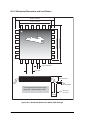
Chapter 29. Package Specifications and Pinout
321
29.1 LQFP Package................................................................................................................................ 321
29.1.1 Pinout ..................................................................................................................................... 321
29.1.2 Mechanical Dimensions and Land Pattern ............................................................................ 322
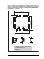
29.2 Ball Grid Array Package ................................................................................................................ 324
29.2.1 Pinout ..................................................................................................................................... 324
29.2.2 Mechanical Dimensions and Land Pattern ............................................................................ 325
29.3 Rabbit Pin Descriptions.................................................................................................................. 327
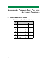
Appendix A. Parallel Port Pins with Alternate Functions
329
A.1 Alternate Parallel Port Pin Outputs ................................................................................................. 329
A.2 Alternate Parallel Port Pin Inputs .................................................................................................... 331
Appendix B. Rabbit 4000 ESD Design Guidelines and Bug Workarounds
333
B.1 ESD Sensitivity................................................................................................................................ 334
B.1.1 ESD Design Guidelines .......................................................................................................... 334
B.2 Bugs ................................................................................................................................................. 335
Index
339
Rabbit 4000 Microprocessor User’s Manual
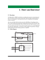
1. THE RABBIT 4000 PROCESSOR
1.1 Introduction
Rabbit Semiconductor was formed expressly to design a a better microprocessor for use in
small- and medium-scale single-board computers. The first microprocessors were the
Rabbit 2000 and the Rabbit 3000. The latest microprocessor is the Rabbit 4000. Rabbit
microprocessor designers have had years of experience using Z80, Z180, and HD64180
microprocessors in small single-board computers. The Rabbit microprocessors share a
similar architecture and a high degree of compatibility with these microprocessors, but
represent a vast improvement.
The Rabbit 4000 is a high-performance microprocessor with low electromagnetic interference (EMI), and is designed specifically for embedded control, communications, and
Ethernet connectivity. The 8-bit Rabbit 4000 outperforms most 16–bit processors without
losing the efficiency of an 8–bit architecture. Extensive integrated features and glueless
architecture facilitate rapid hardware design, while a C-friendly instruction set promotes
efficient development of even the most complex applications.
The Rabbit 4000 is fast, running at up to 60 MHz, with compact code and support for up to
16 MB of memory. Operating with a 1.8 V core and 3.3 or 1.8 V I/O, the Rabbit 4000
boasts an internal 10Base-T Ethernet interface, eight channels of DMA, six serial ports with
IrDA, 40+ digital I/O, quadrature decoder, PWM outputs, and pulse capture and measurement capabilities. It also features a battery-backable real-time clock, glueless memory and
I/O interfacing, and ultra-low power modes. Four levels of interrupt priority allow fast
response to real-time events. Its compact instruction set and high clock speeds give the
Rabbit 4000 exceptionally fast math, logic, and I/O performance.
1.2 Features
The Rabbit 4000 has several powerful design features that practically eliminate EMI problems, which is essential for OEMs that need to pass CE and regulatory radiofrequency
emissions tests. The amplitude of any electromagnetic radiation is reduced by the internal
spectrum spreader, by gated clocks (which prevent unnecessary clocking of unused registers), and by separate power planes for the processor core and I/O pins (which reduce
noise crosstalk). An auxiliary I/O bus can be used by designers to enable separate buses
for I/O and memory or to limit loading the memory bus to reduce EMI and ground bounce
problems when interfacing external peripherals to the processor. The auxiliary I/O bus
accomplishes this by duplicating the Rabbit's data bus on Parallel Port A, and uses Parallel
Chapter 1 The Rabbit 4000 Processor
1
Port B to provide the processor's six or eight least significant address lines for interfacing
with external peripherals.
The high-performance instruction set offers both greater efficiency and execution speed of
compiler-generated C code. Instructions include numerous single-byte opcodes that execute
in two clock cycles, 16-bit and 32-bit loads and stores, 16-bit and 32-bit logical and arithmetic operations, 16 × 16 multiply (executes in 12 clocks), long jumps and returns for
accessing a full 16 megabytes of memory, and one-byte prefixes to turn memory-access
instructions into internal and external I/O instructions. Hardware-supported breakpoints
ease debugging by trapping on code execution or data reads and writes.
The Rabbit 4000 requires no external memory driver or interface-logic. Its 24-bit address
bus, 8-bit or 16-bit data bus, three chip-select lines, two output-enable lines, and two
write-enable lines can be interfaced directly with up to six memory devices. Up to 1 MB
of memory can be accessed directly via the Dynamic C development software, and up to
16 MB can be interfaced with additional software development. A built-in slave port
allows the Rabbit 4000 to be used as master or slave in multi-processor systems, permitting separate tasks to be assigned to dedicated processors. An 8-line data port and five
control signals simplify the exchange of data between devices. A remote cold boot enables
startup and programming via a serial port or the slave port.
The Rabbit 4000 features five 8-bit parallel ports, yielding a total of 40 digital I/O. Six
CMOS-compatible serial ports are available. All six are configurable as asynchronous
(including output pulses in IrDA format), while four are configurable as clocked serial
(SPI) and two are configurable as SDLC/HDLC. The various internal peripherals share the
parallel port’s I/O pins.
The Rabbit 4000 also offers many specialized peripherals. Two input-capture channels
each have a 16-bit counter, clocked by the output of an internal timer, that can be used to
capture and measure pulses. These measurements can be extended to a variety of functions
such as measuring pulse widths or for baud-rate autodetection. Two quadrature decoder
channels each have two inputs, as well as an 8 or 10-bit up/down counter. Each quadrature
decoder channel provides a direct interface to optical encoder units. Four independent pulsewidth modulator (PWM) outputs, each based on a 1024-pulse frame, are driven by the output of a programmable internal timer. The PWM outputs can be filtered to create a 10-bit
D/A converter or they can be used directly to drive devices such as motors or solenoids.
Two external interrupt vectors can multiplex inputs from up to six external pins.
There are numerous timers available for use in the Rabbit 4000. Timer A consists of ten
8-bit counters, each of which has a programmed time constant. Six of them can be cascaded from the primary Timer A counter. Timer B contains a 10-bit counter, two match
registers, and two step registers. An interrupt can be generated or the output pin can be
updated when the counter reaches a match value, and the match value is then incremented
automatically by the step value. Timer C is a 16-bit counter that counts up to a programmable limit. It contains eight match registers, four to set the output of a parallel-port pin
and four to reset it. This allows for the creation of PWM signals (both synchronous and
variable-phase) and quadrature signals.
2
Rabbit 4000 Microprocessor User’s Manual
The Rabbit 4000 also provides support for protected operating systems. Support for two
levels of operation, known as system and user modes, allow application-critical code to
operate in safety while user code is prevented from inadvertently disturbing the setup of
the processor. Memory blocks as small as 4KB can be write-protected against accidental
writes by user code, and stack over/underflows can be trapped by high-priority interrupts.
Security features were also introduced in the Rabbit 4000. Portions of the new instruction
set were introduced to dramatically increase encryption algorithm speeds, and 32 bytes of
battery-backed onchip-encryption RAM store an encryption key away from prying eyes.
The Rabbit 4000 has new peripherals — DMA access and on-chip Ethernet.
The Rabbit 4000 supports eight channels of DMA access to external memory, internal I/O
addresses, and the auxiliary I/O bus. Directing a DMA channel to or from an internal
peripheral such as a serial port or the Ethernet port automatically connects DMA enable
signals. Burst size, priority, and guaranteed cycles for the processor are all under program
control.
The Rabbit 4000 contains a fully featured 10Base-T Ethernet peripheral. Designed to
operate with the DMA peripheral, the Ethernet peripheral is fully compliant with the 802.3
Ethernet standard, including support for auto-negotiation, link detection, multicast filtering, and broadcast addresses. All digital components of the 10Base-T MAC and PHY are
present inside the Rabbit 4000; all that is needed to interface to an Ethernet network is
some simple analog filtering and wave-shaping components.
Chapter 1 The Rabbit 4000 Processor
3
D[7:0]
(8-bit mode)
or
D[15:0]
(16-bit mode)
Data
Buffer
CLK
STATUS
/WDTOUT
SMODE1
SMODE0
/BUFEN
/IORD
/RESET
/IOWR
RESOUT
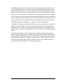
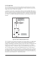
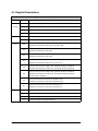
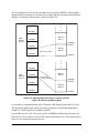
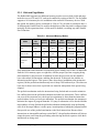
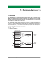
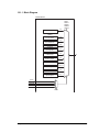
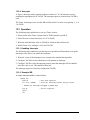
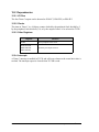
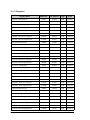
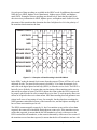
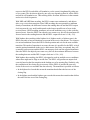
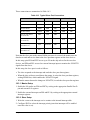
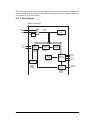
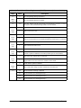
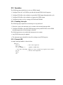
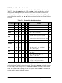
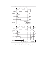
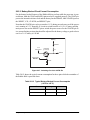
1.3 Block Diagram
External Interface
CPU
CLKI
CLKIEN
Address
Buffer
Memory
Management/
Control
Spectrum
Spreader
Clock
Doubler
Fast
Clock
(15 bits)
A[23:0]
ADDRESS BUS
SYSTEM/USER
Global Power
Save & Clock
Distribution
TIMER C[3:0]
(32 bytes)
Port A
PA [7:0]
Port B
PB[7:0]
Port C
PC[7:0]
Port D
PD[7:0]
Port E
PE[7:0]
Asynch
Serial
Asynch
Bootstrap
Timer B
batterybackable
Synch
Serial
Synch
Bootstrap
TXA, RXA, CLKA,
ATXA, ARXA
Asynch Serial IrDA
IrDA Bootstrap
Secondary
Watchdog
Periodic
Interrupt
Serial Ports
B,C,D
(8 bits)
Real-Time
Clock
DATA BUS
32.768 kHz
Clock Input
Watchdog
Timer
4
Parallel Ports
Serial Port A
VBAT RAM
WAIT
ID[7:0]
IA[7:0]
I[7:0]
/CS2, /CS1, /CS0
/OE1, /OE0
/WE1, /WE0
Timer C
Timer A
CLK32K
Memory Chip
Interface
Asynch
Serial
Synch
Serial
Asynch Serial IrDA
Serial Ports
E, F
Asynch
Serial
HDLC
SDLC
Asynch Serial IrDA
HDLC/SDLC IrDA
TXB, RXB, CLKB,
ATXB, ARXB
TXC, RXC, CLKC
TXD, RXD, CLKD
TXE, RXE
TCLKE, RCLKE
TXF, RXF
TCLKF, RCLKF
External I/O
Chip Interface
Pulse Width
Modulation
PWM[3:0]
INT0A, INT1A
INT0B, INT1B
External
Interrupts
Quadrature
Decoder
QD1A, QD1B
QD2A, QD2B
AQD1A, AQD1B
AQD2A, AQD2B
DREQ0[B:A]
DREQ1[B:A]
DMA
(8 channels)
Input
Capture
20 MHz
/LINK, /ACT
RXD[1:0]
TXD[3:0]
10Base-T
Ethernet
Slave Port
Slave Interface
Bootstrap Interface
PC[7,5,3,1]
PD[7,5,3,1]
PE[7,5,3,1]
SD[7:0]
SA[1:0],
/SCS, /SRD, /SWR,
/SLAVEATTN
Rabbit 4000 Microprocessor User’s Manual
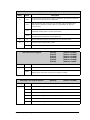
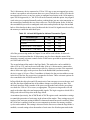
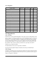
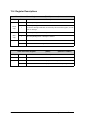
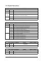
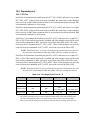
1.4 Basic Specifications
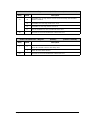
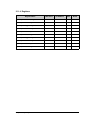
Table 1-1. Rabbit 4000 Specifications and Features
Package
Package Size
128-pin LQFP
128-ball TFBGA
16 mm × 16 mm × 1.5 mm 10 mm × 10 mm × 1.2 mm
Operating Voltage
1.8 V DC core, 3.3 V DC I/O ring
Operating Current
0.35 mA/MHz @ 1.8 V/3.3 V
Operating Temp.
-40°C to +85°C
Maximum Clock Speed
60 MHz
Digital I/O
40+ (arranged in five 8-bit ports)
Serial Ports
6 CMOS-compatible
Ethernet Port
Baud Rate
10Base-T
Clock speed/8 max. asynchronous
Address Bus
20/24-bit
Data Bus
8/16-bit
Timers
Real-Time Clock
RTC Oscillator Circuitry
Watchdog Timer/Supervisor
Clock Modes
Power-Down Modes
Auxiliary I/O Bus
Chapter 1 The Rabbit 4000 Processor
Ten 8-bit, one 10-bit with 2 match registers,
and one 16-bit with 8 match registers
Yes, battery backable
External
Yes
1×, 2×, /2, /3, /4, /6, /8
Sleepy (32 kHz)
Ultra-Sleepy (16, 8, 2 kHz)
8 data, 8 address lines
5
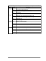
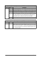
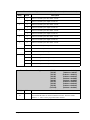
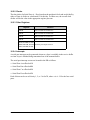
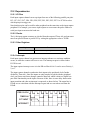
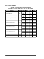
1.5 Comparing Rabbit Microprocessors
The Rabbit 2000, Rabbit 3000, and Rabbit 4000 features are compared below.
Feature
Rabbit 4000
Rabbit 3000
Rabbit 2000
Maximum Clock Speed, industrial
Maximum Clock Speed, commercial
60 MHz
60 MHz
55.5 MHz
58.8 MHz
30 MHz
30 MHz
Maximum Crystal Frequency Main
Oscillator (may be doubled internally up
to maximum clock speed)
60 MHz
30 MHz
30 MHz
32.768 kHz Crystal Oscillator
External
External
Internal
1.8 V ± 10%
3.3 V or 1.8 V
± 10%
3.3 V ± 10%
5.0 V ± 10%
3.6 V
5.5 V
5.5 V
Operating Voltage, core
Operation Voltage, I/O
Maximum I/O Input Voltage
Current Consumption
Number of Package Pins
0.35 mA/MHz
@ 3.3 V
2 mA/MHz @ 3.3 V 4 mA/MHz @ 5 V
128
128
100
Size of Package, LQFP/PQFP
Spacing Between Package Pins
16 × 16 × 1.5 mm
0.4 mm (16 mils)
16 × 16 × 1.5 mm
0.4 mm (16 mils)
24 × 18 × 3 mm
0.65 mm (26 mils)
Size of Package, TFBGA
Spacing Between Package Pins
10 × 10 × 1.2 mm
0.8 mm
10 × 10 × 1.2 mm
0.8 mm
Not available
Separate Power and Ground for I/O
Buffers (EMI reduction)
Yes
Yes
No
Clock Spectrum Spreader
Yes
Yes
Rabbit 2000B/C
Clock Modes
1×, 2×, /2, /3,
/4, /6, /8
1x, 2x, /2, /3
/4, /6, /8
1x, 2x, /4, /8
Powerdown Modes, sleepy
Powerdown Modes, ultra sleepy
32 kHz
16, 8, 2 kHz
32 kHz
16, 8, 2 kHz
Short and
Self-Timed Chip
Selects
Short and
Self-Timed Chip
Selects
None
Yes
Yes
Rabbit 2000C
5
7
5
Yes
Yes
None
6
6
4
4 (A, B, C, D)
4 (A, B, C, D)
2 (A, B)
2 (E, F)
2 (E, F)
None
Low-Power Memory Control
Extended Memory Timing for HighFrequency Operation
Number of 8-bit I/O Ports
Auxiliary I/O Data/Address Bus
Number of Serial Ports
Serial Ports Capable of SPI/Clocked Serial
Serial Ports Capable of SDLC/HDLC
6
32 kHz
Rabbit 4000 Microprocessor User’s Manual
Feature
Rabbit 4000
Rabbit 3000
Rabbit 2000
Asynch Serial Ports With Support for
IrDA Communication
6
6
None
Serial Ports with Support for SDLC/
HDLC IrDA Communication
2
2
None
Maximum Asynchronous Baud Rate
Clock Speed/8
Clock Speed/8
Clock Speed/32
10Base-T
None
None
2
2
None
Ethernet Port
Input Capture Units
Chapter 1 The Rabbit 4000 Processor
7
8
Rabbit 4000 Microprocessor User’s Manual
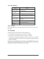
2. CLOCKS
2.1 Overview
The Rabbit 4000 supports up to three separate clocks—the main clock, the 32 kHz clock,
and the 20 MHz Ethernet clock. The main clock is used to derive the processor clock and
the peripheral clock inside the processor. The 32 kHz clock is used to drive the asynchronous serial bootstrap, the real-time clock, the periodic interrupt, and the watchdog timers.
The Rabbit 4000 has a spectrum spreader on the main clock that shortens and lengthens
clock cycles. This has the net effect of reducing the peak energy of clock harmonics by
spreading the spectral energy into nearby frequencies, which reduces EMI and facilitates
government-mandated EMI testing. Gated clocks are used whenever possible to avoid
clocking unused portions of the processor, and separate power-supply pins for the core and
I/O ring further reduce EMI from the Rabbit 4000.
The main clock can be doubled or divided by 2, 4, 6, or 8 to reduce EMI and power consumption. The 32 kHz clock (which can be divided by 2, 4, 8, or 16) can be used instead of
the main clock to generate processor and peripheral clocks as low as 2 kHz for significant
power savings. Note that dividing the 32 kHz clock only affects the processor and peripheral clocks; the full 32 kHz signal is still provided to the peripherals (RTC and watchdog
timers) that use it directly. The periodic interrupt is automatically disabled since there is
not enough time to process it when running off the 32 kHz clock.
The Ethernet clock can be driven by the processor clock, the processor clock divided by 2,
or by the input on PE6. The Ethernet clock needs to be 20 MHz to conform to the 10Base-T
specification. See Chapter 20 for more details on the Ethernet clock.
Chapter 2 Clocks
9
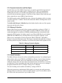
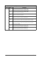
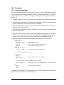
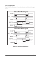
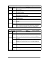
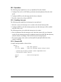
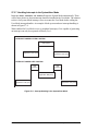
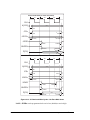
2.1.1 Block Diagram
NACR
PE6
Ethernet
Clock
CLKIEN
Clock
Disable
MAIN CLOCK
Divide
by 2
GCSR
CLKI
Spectrum
Spreader
Clock
Doubler
Divide by
2, 4, 6, 8
GCMxR
GCDR
GCSR
GCSR
CPU Clock
Peripheral Clock
Divide by
2, 4, 8, 16
CLK32K
GPSCR
GOCR
CLK Pin
Divide
by 2
Real-Time Clock
Periodic Interrupt
Asynch. Serial Bootstrap
Watchdog Timer
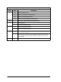
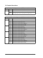
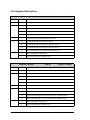
2.1.2 Registers
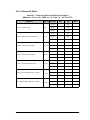
Register Name
Mnemonic
I/O Address
R/W
Reset
GCSR
0x0000
R/W
11000000
Global Clock Modulator 0 Register
GCM0R
0x000A
W
00000000
Global Clock Modulation 1 Register
GCM1R
0x000B
W
00000000
GCDR
0x000F
R/W
00000000
Global Control/Status Register
Global Clock Double Register
10
Rabbit 4000 Microprocessor User’s Manual
2.2 Dependencies
2.2.1 I/O Pins
The main clock input is on the CLKI pin. There is an internal Schmitt trigger on this pin to
remove problems with noise on slowly-transitioning signals.
The main clock disable output is on the CLKIEN pin. Its state is changed by one of the bit
combinations of bits 4:2 in GCSR.
The 32 kHz clock input is on the CLK32K pin. There is an internal Schmitt trigger on this
pin as well.
The peripheral clock or peripheral clock divided by 2 may be optionally output on the CLK
pin by enabling it via bits 7:6 in GOCR.
The Ethernet clock may be input on pin PE6 by enabling it via bits 7:6 in NACR. It may be
set to use the processor clock or processor clock divided by 2 in that register as well. Note
that there is not an internal Schmitt trigger on PE6; it is highly recommended that an external Schmitt trigger be placed on this pin if it is to be used as the Ethernet clock.
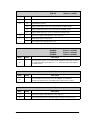
2.2.2 Other Registers
Register
Function
GOCR
Used to set up the CLK output pin.
NACR
Used to set up the Ethernet clock.
Chapter 2 Clocks
11
2.3 Operation
2.3.1 Main Clock
The main clock is input on the CLKI pin, and is optionally sent through the spectrum
spreader and then the clock doubler. Both of these are described in greater detail below.
Different main clock modes may be selected via the GCSR, as shown in Table 2-1. Note
that one GCSR setting slows the processor clock while the peripheral clock operates at full
speed; this allows some power reduction while keeping settings like serial baud rates and
the PWM at their desired values.
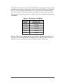
Table 2-1. Clock Modes
GCSR Setting
Processor Clock
Peripheral Clock
xxx010xx
Main clock
Main clock
xxx011xx
Main clock / 2
Main clock / 2
xxx110xx
Main clock / 4
Main clock / 4
xxx111xx
Main clock / 6
Main clock / 6
xxx000xx
Main clock / 8
Main clock / 8 (default on startup)
xxx001xx
Main clock / 8
Main clock
xxx100xx
32 kHz clock (possibly divided)
32 kHz clock (possibly divided
via GPSCR)
xxx101xx
32 kHz clock (possibly divided);
main clock disabled via CLKIEN
output signal
32 kHz clock (possibly divided
via GPSCR)
When the 32 kHz clock is enabled in GCSR, it can be further divided by 2, 4, 6, or 8 to
generate even lower frequencies by enabling those modes in bits 0–2 of GPSCR. See
Table 2-4 for more details.
12
Rabbit 4000 Microprocessor User’s Manual
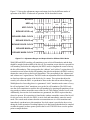
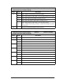
2.3.2 Spectrum Spreader
When enabled, the spectrum spreader stretches and compresses the main clock in a complex
pattern that spreads the energy of the clock harmonics over a wider range of frequencies.
0
AMPLITUDE (dB)
-10
Spectrum Spreader
Disabled
Spectrum Spreader
Enabled (normal setting)
-20
-30
-40
-50
400
405
410
415
420
425
430
435
440
445
FREQUENCY (MHz)
Figure 2-1. Effects of Spectrum Spreader
There are three settings that correspond to normal and strong spreading in the 0–50 MHz
and >50 MHz main clock range. Each setting will affect the clock cycle differently; the
maximum cycle shortening (at 1.8 V and 25°C) is shown in Table 2-2 below.
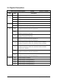
Table 2-2. Spectrum Spreader Settings
0–50 MHz
> 50 MHz
GCM0R
Value
Description
Max. Cycle
Shortening
—
Normal
0x40
Normal spreading of frequencies over
50 MHz
2.3 ns
Normal
Strong
0x00
Normal spreading of frequencies up to
50 MHz; strong spreading of
frequencies over 50 MHz
3 ns
Strong
—
0x80
Strong spreading of frequencies up to
50 MHz; normal spreading of
frequencies over 50 MHz
4.5 ns
Chapter 2 Clocks
13
The spectrum spreader either stretches or shrinks the low plateau of the clock by a maximum of 3 ns for the normal spreading and up to 5 ns for the strong spreading. If the clock
doubler is used, this will cause an additional asymmetry between alternate clock cycles.
Harmonics (dB)
Both normal and strong modes reduce clock harmonics by approximately 15 dB for frequencies above 100 MHz; for lower frequencies the strong setting has a greater effect in
reducing the peak spectral strength as shown in Figure 2-2.
15
Strong Spreading
10
Normal Spreading
5
50
100
150
200
250
300
350
Frequency (MHz)
Figure 2-2. Peak Spectral Amplitude Reduction by Spectrum Spreader
Two registers control the clock spectrum spreader. These registers must be loaded in a specific manner with proper time delays. GCM0R is only read by the spectrum spreader at the
moment when the spectrum spreader is enabled by storing 0x080 in GCM1R. If GCM1R
is cleared (when disabling the spectrum spreader), there is up to a 500-clock delay before
the spectrum spreader is actually disabled. The proper procedure is to clear GCM1R, wait
for 500 clocks, set GCM0R, and then enable the spreader by storing 0x080 in GCM1R.
The spectrum spreader is applied to the main clock before the clock doubler, so if both are
enabled there will be additional asymmetry between alternate clock cycles.If the clock
doubler is used, the spectrum spreader affects every other cycle and reduces the clock high
time. If the doubler is not used, then the spreader affects every clock cycle, and the clock
low time is reduced.
14
Rabbit 4000 Microprocessor User’s Manual
2.3.3 Clock Doubler
The clock doubler allows a lower frequency crystal to be used for the main oscillator and
to provide an added range over which the clock frequency can be adjusted. The clock doubler is controlled via the Global Clock Double Register (GCDR).
The clock doubler uses an on-chip delay circuit that must be programmed by the user at
startup if there is a need to double the clock. Table 2-3 lists the recommended delays for
the GCDR for various oscillator frequencies.
Table 2-3. Recommended Delays Set In GCDR for Clock Doubler
Chapter 2 Clocks
Recommended GCDR Value
Frequency Range
0x0F
≤7.3728 MHz
0x0B
7.3728–11.0592 MHz
0x09
11.0592–16.5888 MHz
0x06
16.5888–20.2752 MHz
0x03
20.2752–52.8384 MHz
0x01
52.8384–70.0416 MHz
0x00
>70.0416 MHz
15
When the clock doubler is used and there is no subsequent division of the clock, the output
clock will be asymmetric, as shown in Figure 2-3.
P
Oscillator
48%
52%
0.48P
0.52P
Oscillator delayed
and inverted
Doubled clock
Delay
time
Example
Write
Cycle
0.48P
0.52P
Address / CS
Data out
Write pulse
Early write pulse
option
Address / CS
Example
Read
Cycle
Data out from mem
Output enb
Early output enb
option
Figure 2-3. Effect of Clock Doubler
The doubled-clock low time is subject to wide (50%) variation since it depends on process
parameters, temperature, and voltage. The times given above are for a core supply voltage
of 1.8 V and a temperature of 25°C. The values increase or decrease by 1% for each 5°C
increase or decrease in temperature. The doubled clock is created by xor’ing the delayed
and inverted clock with itself. If the original clock does not have a 50-50 duty cycle, then
alternate clocks will have a slightly different length. Since the duty cycle of the built-in
oscillator can be as asymmetric as 52% / 48%, the clock generated by the clock doubler
will exhibit up to a 4% variation in period on alternate clocks. Memory access time is not
affected because memory bus cycle is 2 clocks long and includes both a long and a short
16
Rabbit 4000 Microprocessor User’s Manual
clock, resulting in no net change due to asymmetry. However, if an odd number of wait
states is used, then the memory access time will be affected slightly
The maximum allowed clock speed must be slightly reduced if the clock is supplied via
the clock doubler. The only signals clocked on the falling edge of the clock are the memory and I/O write pulses and the early option memory output enable. See Chapter 5 for
more information on the early output enable and write enable options.
The power consumption is proportional to the clock frequency, and for this reason power
can be reduced by slowing the clock when less computing activity is taking place. The
clock doubler provides a convenient method of temporarily speeding up or slowing down
the clock as part of a power management scheme.
Chapter 2 Clocks
17
2.3.4 32 kHz Clock
The 32.768 kHz clock is used to drive the asynchronous serial bootstrap, the real-time
clock, the periodic interrupt, and the watchdog timers. If these features are not used in a
design, the use of the 32 kHz clock is optional.
A simplified version of the recommended oscillator circuit for the Rabbit 4000 is shown
below. The values of resistors and capacitors may need to be adjusted for various frequencies and crystal load capacitances. Technical Note TN235, “External 32.768 kHz Oscillator Circuits“, is available on the Rabbit Semiconductor web site and goes into this circuit
in detail.
VBAT
R1
Cin
R1 and R2 control the
power consumed by the
unbuffered inverter.
SN74AHC1GU04
U1A
R2
U2A
NC7SP14
Rp
Rs
CL = 5-12 pF
32.768 kHz
C1
C2
C1 values may vary or
C1 may be eliminated
Figure 2-4. Basic 32.768 kHz Oscillator Circuit
The 32.768 kHz circuit consumes microampere level currents and has a very high impedance, making it susceptible to noise, moisture, and environmental contaminants. It is
strongly recommended to conformally coat this circuit to limit effects of temperature and
humidity on the oscillation frequency. Details about this requirement are available in
Technical Note TN303, “Conformal Coating”, from the Rabbit Semiconductor Web site.
The 32.768 kHz oscillator is slow to start oscillating after power-on. For this reason, a
wait loop in the BIOS waits until this oscillator is oscillating regularly before continuing
the startup procedure. If the clock is battery-backed, there will be no startup delay since
the oscillator is already oscillating. The startup delay may be as much as 5 seconds. Crystals with low series resistance (R < 35 kΩ) will start faster.
18
Rabbit 4000 Microprocessor User’s Manual
The 32 kHz oscillator can be used to drive as the processor and peripheral clock to provide
significant power savings in “ultra-sleepy” modes. The 32 kHz oscillator can be divided
by 2, 4, 8, or 16 to provide clock speeds as low as 2.048 kHz. Special self-timed chip
selects are available to keep the memory devices enabled for as short a time as possible
when an ultra-sleepy mode is enabled; see Chapter 26 for more details on reducing power
consumption.
Table 2-4. Ultra-Sleepy Clock Modes
GPSCR
Setting
Processor and
Peripheral Clock
xxxxx000
32.768 kHz
xxxxx100
16.384 kHz
xxxxx101
8.192 kHz
xxxxx110
4.096 kHz
xxxxx111
2.048 kHz
When the 32 kHz clock is enabled, the periodic interrupt is disabled automatically. The
real-time clock and watchdog timers keep running, and use the full 32 kHz clock even
when the processor and peripheral clocks use a divider on the 32 kHz clock.
Chapter 2 Clocks
19
2.4 Register Descriptions
Global Control/Status Register
(GCSR)
(Address = 0x0000)
Bit(s)
Value
7:6
00
No reset or watchdog timer timeout since the last read.
(rd-only)
01
The watchdog timer timed out. These bits are cleared by a read of this register.
10
This bit combination is not possible.
11
Reset occurred. These bits are cleared by a read of this register.
0
No effect on the periodic interrupt. This bit will always be read as zero.
1
Force a periodic interrupt to be pending.
5
4:2
1:0
20
Description
000
Processor clock from the main clock, divided by 8.
Peripheral clock from the main clock, divided by 8.
001
Processor clock from the main clock, divided by 8.
Peripheral clock from the main clock.
010
Processor clock from the main clock.
Peripheral clock from the main clock.
011
Processor clock from the main clock, divided by 2.
Peripheral clock from the main clock, divided by 2.
100
Processor clock from the 32 kHz clock, optionally divided via GPSCR.
Peripheral clock from the 32 kHz clock, optionally divided via GPSCR.
101
Processor clock from the 32 kHz clock, optionally divided via GPSCR.
Peripheral clock from the 32 kHz clock, optionally divided via GPSCR.
The main clock is disabled.
110
Processor clock from the main clock, divided by 4.
Peripheral clock from the main clock, divided by 4.
111
Processor clock from the main clock, divided by 6.
Peripheral clock from the main clock, divided by 6.
00
Periodic interrupts are disabled.
01
Periodic interrupts use Interrupt Priority 1.
10
Periodic interrupts use Interrupt Priority 2.
11
Periodic interrupts use Interrupt Priority 3.
Rabbit 4000 Microprocessor User’s Manual
Global Clock Modulator 0 Register
(GCM0R)
(Address = 0x000A)
Bit(s)
Value
7:6
00
Clock dither in 1 ns steps, from 0 ns to 26 ns. Do not modify while the dither
function is enabled.
01
Clock dither in 0.5 ns steps, from 0 ns to 13 ns.
10
Clock dither in 2 ns steps, from 0 ns to 52 ns.
11
This bit combination is reserved and must not be used.
5:0
Description
These bits are reserved and should be written with zeros.
Global Clock Modulator 1 Register
(GCM1R)
(Address = 0x000B)
Bit(s)
Value
7
0
Disable the clock dither function. Disable does not take effect until the dither
pattern has returned to the 0 ns base delay value.
1
Enable the clock dither function.
6:0
Chapter 2 Clocks
Description
These bits are reserved and should be written with zeros.
21
Global Clock Double Register
Bit(s)
Value
7:5
4:0
22
(GCDR)
(Address = 0x000F)
Description
These bits are reserved and should be written with zeros.
00000
The clock doubler circuit is disabled.
00001
6 ns nominal low time.
00010
7 ns nominal low time.
00011
8 ns nominal low time.
00100
9 ns nominal low time.
00101
10 ns nominal low time.
00110
11 ns nominal low time.
00111
12 ns nominal low time.
01000
13 ns nominal low time.
01001
14 ns nominal low time.
01010
15 ns nominal low time.
01011
16 ns nominal low time.
01100
17 ns nominal low time.
01101
18 ns nominal low time.
01110
19 ns nominal low time.
01111
20 ns nominal low time.
10001
3 ns nominal low time.
10010
4 ns nominal low time.
10011
5 ns nominal low time.
other
Any bit combination not listed is reserved and must not be used.
Rabbit 4000 Microprocessor User’s Manual
Global Output Control Register
(GOCR)
(Address = 0x000E)
Bit(s)
Value
7:6
00
CLK pin is driven with peripheral clock.
01
CLK pin is driven with peripheral clock divided by 2.
10
CLK pin is low.
11
CLK pin is high.
00
STATUS pin is active (low) during a first opcode byte fetch.
01
STATUS pin is active (low) during an interrupt acknowledge.
10
STATUS pin is low.
11
STATUS pin is high.
00
/WDTOUT pin functions normally.
01
Enable /WDTOUT for test mode. Rabbit Semiconductor internal use only.
10
/WDTOUT pin is low (1 cycle min, 2 cycles max, of 32 kHz).
11
This bit combination is reserved and should not be used.
00
/BUFEN pin is active (low) during external I/O cycles.
01
/BUFEN pin is active (low) during data memory accesses.
10
/BUFEN pin is low.
11
/BUFEN pin is high.
5:4
3:2
1:0
Chapter 2 Clocks
Description
23
Network Port A Control Register
Bit(s)
Value
7:6
00
Disable the Ethernet clock.
01
Ethernet clock from PE6 on Parallel Port E.
10
Ethernet clock from peripheral clock.
11
Ethernet clock from peripheral clock divided by 2.
5:4
3
2
1
0
24
(NACR)
(Address = 0x0207)
Description
These bits are unused and should be written with zero.
0
Normal operation.
1
Restart auto-negotiation process.
0
Disable auto-negotiation function.
1
Enable auto-negotiation function.
0
Force half-duplex operation. If auto-negotiation is enabled, only half-duplex
operation will be advertised.
1
Enable full-duplex operation. If auto-negotiation is disabled, this forces fullduplex operation. If auto-negotiation is enabled, this allows advertising fullduplex capability.
This bit is unused and should be written with zero.
Rabbit 4000 Microprocessor User’s Manual
3. RESET AND BOOTSTRAP
3.1 Overview
The Rabbit 4000’s /RESET pin initializes everything in the processor except for the realtime clock registers and the contents of the battery-backed onchip-encryption RAM. If a
write cycle is in progress, it waits until the write cycle is completed to avoid potential
memory corruption.
After reset, the Rabbit 4000 checks the state of the SMODE pins. Depending on their
state, it either begins normal operation by fetching instruction bytes from /CS0 and /OE0,
or it enters a special bootstrap mode where it fetches bytes from either Serial Port A or the
slave port. In this mode, bytes can be written to internal registers to set up the Rabbit 4000
for a particular configuration, or to memory to load a program. The processor can begin
normal operation once the bootstrap operation is completed.
3.1.1 Block Diagram
Reset
RESOUT
/RESET
Reset
Delay
Master Reset
Rabbit
4000
CPU
Clock
Bootstrap
SPCR
Asynch Serial Bootstrap
SMODE0
SMODE1
Bootstrap
Selection
Clocked Serial Bootstrap
Slave Port Bootstrap
Normal Operation
Chapter 3 Reset and Bootstrap
25
3.1.2 Registers
Register Name
Slave Port Control Register
Mnemonic
I/O Address
R/W
Reset
SPCR
0x0024
R/W
0xx00000
3.2 Dependencies
3.2.1 I/O Pins
SMODE0, SMODE1 — When the Rabbit 4000 is first powered up or when it is reset, the
state of the SMODE0 and SMODE1 pins controls its operation.
/RESET — Pulling the /RESET pin low will initialize everything in the Rabbit 4000
except for the real-time clock registers and the onchip-encryption RAM.
/CS1 — During reset the impedance of the /CS1 pin is high, and all other memory and I/O
control signals are held high. The special behavior of /CS1 allows an external RAM to be
powered by the same source as the VBATIO pin (which powers /CS1). In this case, a pullup resistor is required on /CS1 to keep the RAM deselected during powerdown.
RESOUT — The RESOUT pin is high during reset and powerdown, but low at all other
times, and can be used to control an external power switch to disconnect VDDIO from
VBATIO when the main power source is removed.
3.2.2 Clocks
The processor requires a 32 kHz clock input to generate the 2400 bps internal clock
required for asynchronous serial bootstrap. No 32 kHz clock is required for either clocked
serial or slave port bootstrap.
When the processor comes out of reset, the CPU clock and peripheral clocks are both in
divide-by-8 mode.
3.2.3 Other Registers
Register
SPCR
Function
Enable/disable processor monitoring of SMODE
pins; read current state of SMODE pins.
3.2.4 Interrupts
There are no interrupts associated with reset or bootstrap.
26
Rabbit 4000 Microprocessor User’s Manual
3.3 Operation
Pulling the /RESET pin low will initialize everything in the Rabbit 4000 except for the
real-time clock registers and the onchip-encryption RAM. The reset of the Rabbit 4000 is
delayed until the completion of any write cycles in progress; reset takes effect immediately when no write cycles are occurring. The reset sequence requires a minimum of 128
cycles of the main clock to complete in either case.
During reset, the impedance of the /CS1 pin is high and all other memory and I/O control
signals are held high. The special behavior of /CS1 allows an external RAM to be powered
by the same source as the VBATIO pin (which powers /CS1). In this case, a pullup resistor
is required on /CS1 to keep the RAM deselected during powerdown. The RESOUT pin is
high during reset and powerdown, but low at all other times, and can be used to control an
external power switch to disconnect VDDIO from VBATIO when the main power source
is removed.
Table 3-1 lists the condition of the processor after reset takes place. The state of all registers after reset is provided in the chapter describing the specific peripheral.
Table 3-1. Rabbit 4000 Condition After Reset
Function
Operation After Reset
CPU Clock,
Peripheral Clock
Divide-by-8 mode
Clock Doubler,
Clock Dither
Disabled
Memory Bank 0
Control Register
/CS0, /OE0, write-protected,
4 wait states
Memory Advanced
Control Register
8-bit interface
CPU Registers:
PC, SP, IIR, EIR,
SU, HTR
0x0000
Interrupt Priority
(IP Register)
0xFF (Priority 3)
Watchdog Timer
Enabled (2 seconds)
Secondary
Watchdog Timer
Disabled
The processor checks the SMODE pins after the /RESET signal is inactive. Table 3-2
summarizes what happens:
• If both SMODE pins are zero, the Rabbit 4000 begins fetching instructions from the
memory device on /CS0 and /OE0. If a 16-bit memory is used on /CS0, the first section
of code must immediately select the 16-bit bus mode. Chapter 5 provides a short program to do this.
Chapter 3 Reset and Bootstrap
27
• If either of the SMODE pins is high, the processor will enter the bootstrap mode and
accept triplets from either Serial Port A or the slave port. It is good practice to place
pulldown resistors on the SMODE pins to ensure proper operation of your design.
Table 3-2. SMODE Pin Settings
SMODE Pins [1,0]
Operation
00
No bootstrap; code is fetched from address 0x0000
on /CS0, /OE0.
01
Bootstrap from the slave port.
10
Bootstrap from Serial Port A, clocked mode.
11
Bootstrap from Serial Port A, asynchronous mode.
In bootstrap mode, the processor inhibits the normal memory fetch from /CS0 and instead
fetches instructions from a small internal boot ROM. This program reads triplets of three
bytes from the selected peripheral. The first byte is the most-significant byte of a 16-bit
address, the second byte is the least-significant byte of the address, and the third byte is
the data to be written. If the uppermost bit of the address is 1, then the address is assumed
to be an internal register address instead of a memory address, and the data are written to
the appropriate register instead.
The boot ROM program waits for data to be available; each byte received automatically
resets the watchdog timer with a 2-second timeout. Bytes must be received quickly
enough to prevent timeout (or the watchdog must be disabled).
The device checks the state of the SMODE pins each time it jumps back to the start of the
ROM program and responds according to the current state. In addition, by writing to bit 7
of the Slave Port Control Register (SPCR) the processor can be told to ignore the state of
the SMODE pins and continue normal operation.
Note that the processor can be told to reenter bootstrap mode at any time by setting bit 7 of
SPCR low; once this occurs and the least-significant four bits of the current PC address
are zero, the processor will sample the state of the SMODE pins and respond accordingly.
This feature allows in-line downloading from the selected bootstrap port; once the download is complete, bit 7 of SPCR can be set high and the processor will continue operating
from where it left off.
As a security feature, any attempt to enter bootstrap mode from either the SMODE pins or
by writing to bit 7 of SPCR will erase the data stored in the onchip-encryption RAM. This
prevents loading a small program in memory to read out the data.
28
Rabbit 4000 Microprocessor User’s Manual
3.4 Register Descriptions
Slave Port Control Register
(SPCR)
Bit(s)
Value
7
0
Program fetch as a function of the SMODE pins.
1
Ignore the SMODE pins program fetch function.
6:5
4:2
1:0
(Address = 0x0024)
Description
Read
These bits report the state of the SMODE pins.
Write
These bits are ignored and should be written with zero.
000
Disable the slave port. Parallel Port A is a byte-wide input port.
001
Disable the slave port. Parallel Port A is a byte-wide output port.
010
Enable the slave port, with /SCS from Parallel Port E bit 7.
011
Enable the auxiliary I/O bus. Parallel Port A is used for the data bus and Parallel
Port B[7:2] is used for the address bus.
100
This bit combination is reserved and should not be used.
101
This bit combination is reserved and should not be used.
110
Enable the slave port, with /SCS from Parallel Port B bit 6.
111
Enable the auxiliary I/O bus. Parallel Port A is used for the data bus and Parallel
Port B[7:0] is used for the address bus.
00
Slave port interrupts are disabled.
01
Slave port interrupts use Interrupt Priority 1.
10
Slave port interrupts use Interrupt Priority 2.
11
Slave port interrupts use Interrupt Priority 3.
Chapter 3 Reset and Bootstrap
29
30
Rabbit 4000 Microprocessor User’s Manual
4. SYSTEM MANAGEMENT
4.1 Overview
There are a number of basic system peripherals in the Rabbit 4000 processor, some of
which are covered in later chapters. The peripherals covered in this chapter are the periodic
interrupt, the real-time clock, the watchdog timers, the battery-backed onchip-encryption
RAM, and some of the miscellaneous output pins and their control and processor registers
that provide the processor ID and revision numbers.
The periodic interrupt, when enabled, is generated every 16 clocks of the 32 kHz clock
(every 488 µs, or 2.048 kHz). This interrupt can be used to perform periodic tasks.
The real-time clock (RTC) consists of a 48-bit counter that is clocked by the 32 kHz clock.
It is powered by the VBAT pin, and so can be battery-backed. The value in the counter is
not affected by reset, and can only be set to zero by writing to the RTC control register.
The 48-bit width provides a 272-year span before rollover occurs.
There are two watchdog timers in the Rabbit 4000, both clocked by the 32 kHz clock. The
main watchdog timer can be set to time out from 250 ms to 2 seconds, and resets the processor if not reloaded within that time. Its purpose is to restart the processor when it
detects that a program gets stuck or disabled.
The secondary watchdog timer can time out from 30.5 µs up to 7.8 ms, and generates a
Priority 3 secondary watchdog interrupt when it is not reset within that time. The primary
use for the secondary watchdog is to act as a safety net for the periodic interrupt — if the
secondary watchdog is reloaded in the periodic interrupt, it will count down to zero if the
periodic interrupt stops occurring. In addition, it can be used as a periodic interrupt on its
own.
The battery-backed onchip-encryption RAM consists of 32 bytes of memory that are
powered by the VBAT pin. Their values are not affected by reset, but are erased if the state
of the SMODE pins changes. These 32 bytes are intended for storing sensitive data (such
as an encryption key) somewhere other than an external memory device. The “tamperprotection” erase feature prevents loading a program into the onchip-encryption RAM via
the programming port and reading out the bytes.
The following other registers are also described in this chapter.
• Global Output Control Register (GOCR), which controls the behavior of the CLK,
STATUS, /WDT, and /BUFEN pins
• Global CPU Register (GCPU), which holds the identification number of the processor.
• Global Revision Register (GREV), which hold the revision number of the processor.
Chapter 4 System Management
31
4.1.1 Block Diagram
Basic System Peripherals
32 kHz Clock
Periodic Interrupt
(488 µs)
Interrupt
Generation
Interrupt
Request
GCSR
Real-Time Clock
RTCxR
RTCCR
Master Reset
/WDTOUT Pin
Watchdog
Timer
WDTCR
WDTTR
Interrupt
Generation
Secondary
Watchdog Timer
Interrupt
Request
WDTCR
SWDTR
4.1.2 Registers
Mnemonic
I/O Address
R/W
Reset
Global Control/Status Register
GCSR
0x0000
R/W
11000000
Real-Time Clock Control Register
RTCCR
0x0001
W
00000000
Real-Time Clock Byte 0 Register
RTC0R
0x0002
R/W
xxxxxxxx
Real-Time Clock Byte 1 Register
RTC1R
0x0003
R
xxxxxxxx
Real-Time Clock Byte 2 Register
RTC2R
0x0004
R
xxxxxxxx
Real-Time Clock Byte 3 Register
RTC3R
0x0005
R
xxxxxxxx
Real-Time Clock Byte 4 Register
RTC4R
0x0006
R
xxxxxxxx
Real-Time Clock Byte 5 Register
RTC5R
0x0007
R
xxxxxxxx
Watchdog Timer Control Register
WDTCR
0x0008
W
00000000
Watchdog Timer Test Register
WDTTR
0x0009
W
00000000
Secondary Watchdog Timer Register
SWDTR
0x000C
W
11111111
Global Output Control Register
GOCR
0x000E
R/W
00000000
Global CPU Configuration Register
GCPU
0x002E
R
0xx00010
Global Revision Register
GREV
0x002F
R
0xx00000
VRAM00–
VRAM1F
0x0600–0x061F
R/W
xxxxxxxx
Register Name
Battery-Backed Onchip-Encryption RAM Byte
00–1F
32
Rabbit 4000 Microprocessor User’s Manual
4.2 Dependencies
4.2.1 I/O Pins
The CLK, STATUS, /WDTOUT, and /BUFEN pins are controlled by GOCR. Each of
these pins can be used as general-purpose outputs by driving them high or low:
• the CLK pin can output the peripheral clock, the peripheral clock divided by two, or be
driven high or low;
• the STATUS pin can be active low during the first byte of each opcode fetch, active low
during an interrupt acknowledge, or driven high or low;
• the /WDTOUT pin can be active low whenever the watchdog timer resets the device or
driven low; and
• the /BUFEN pin can be active low during external I/O cycles, active low during data
memory cycles, or driven high or low.
The values in the battery-backed onchip-encryption RAM bytes are cleared If the signal
on the SMODE pins changes state.
4.2.2 Clocks
The periodic interrupt, real-time clock, watchdog timer, and secondary watchdog timer
require the 32 kHz clock.
4.2.3 Interrupts
The periodic interrupt is enabled in GCSR, and will occur every 488 µs. It is cleared by
reading GCSR. It can operate at Priority 1, 2, or 3.
The secondary watchdog interrupt will occur whenever the secondary watchdog is
enabled and allowed to count down to zero. It is cleared by restarting the secondary watchdog by writing to WDTCR. The secondary watchdog interrupt always occurs at Priority 3.
Chapter 4 System Management
33
4.3 Operation
4.3.1 Periodic Interrupt
The following steps explain how a periodic interrupt is used.
1. Write the vector to the interrupt service routine to the internal interrupt table.
2. Enable the periodic interrupt by writing to GCSR.
3. The interrupt request is cleared by reading from GCSR.
A sample interrupt handler is shown below.
periodic_isr::
push af
ioi ld a, (GCSR)
; clear the interrupt request and get status
; handle any periodic tasks here
pop af
ipres
ret
4.3.2 Real-Time Clock
The real-time clock consists of six 8-bit registers that together comprise a 48-bit value.
The real-time clock is not synchronized to the read operation, so the least-significant bit
should be read twice and checked for matching values; if the two reads do not match, then
the real-time clock may have been updating during the read and should be read again.
Writing to RTC0R latches the current real-time clock value into the RTCxR holding registers, so the following sequence should be used to read the real-time clock.
1. Write any value to RTC0R and then read back a value from RTC0R.
2. Write a value to RTC0R again, and again read back a value from RTC0R.
3. If the two values do not match, repeat Step 2 until the last two readings are identical.
4. At this point, registers RTC1R through RTC6R can also be read and used.
Note that the periodic interrupt and the real-time clock are clocked by the same edge of the
32 kHz clock; if read from the periodic interrupt, the count is guaranteed to be stable and
only needs to be read once (assuming it occurs within one clock of the 32 kHz clock).
The real-time clock can be reset by writing the sequence 0x40 – 0x80 to RTCCR. It can be
reset and left in the byte increment mode by writing 0x40 – 0xC0 to RTCCR and then
writing bytes repeatedly to RTCCR to increment the appropriate bytes of the real-time
clock. The byte increment mode is disabled by writing 0x00 to RTCCR.
34
Rabbit 4000 Microprocessor User’s Manual
4.3.3 Watchdog Timer
The watchdog timer is enabled on reset with a 2-second timeout. Unless specific data are
written to WDTCR before that time expires, the processor will be reset. The watchdog
timer can be disabled by writing a sequence of two bytes to WDTTR as described in the
register description.
Table 4-1. Watchdog Timer Settings
WDTCR Value
Effect
0x5A
Restart watchdog timer with 2-second timeout.
0x57
Restart watchdog timer with 1-second timeout.
0x59
Restart watchdog timer with 500-millisecond timeout.
0x53
Restart watchdog timer with 250-millisecond timeout.
0x5F
Restart the secondary watchdog timer.
The watchdog timer also contains a special test mode that speeds up the timeout period by
clocking it with the peripheral clock instead of the 32 kHz clock. This mode can be
enabled by writing to WDTTR.
4.3.4 Secondary Watchdog Timer
The secondary watchdog timer is disabled on reset, unless the reset occurs because the
primary watchdog timer times out while the secondary watchdog timer is enabled. The
BIOS provided by Rabbit Semiconductor in Dynamic C avoids this bug by disabling the
secondary watchdog on startup or reset by writing 0x5F to WDTCR. The following steps
explain how to use the secondary watchdog timer.
1. Write the vector to the interrupt service routine to the internal interrupt table.
2. Write the desired timeout period to SWDTR. This also enables the secondary watchdog
timer.
3. Restart the secondary watchdog timer by either writing the timeout period to SWDTR
or writing 0x5F to WDTCR.
If the secondary watchdog timer counts down to zero, a Priority 3 secondary watchdog
interrupt will occur. This interrupt request is cleared by writing a new timeout value to
SWDTR. A sample interrupt handler is shown below.
secwd_isr::
push af
; determine why the interrupt occurred and take appropriate action
ld a, 0x40
ioi ld (SWDTR), a
; timeout period of 0x40/32kHz = 1.95ms
; clear the interrupt request
pop af
ipres
ret
Chapter 4 System Management
35
4.4 Register Descriptions
Global Control/Status Register
(GCSR)
(Address = 0x0000)
Bit(s)
Value
7:6
00
No reset or watchdog timer timeout since the last read.
(rd-only)
01
The watchdog timer timed out. These bits are cleared by a read of this register.
10
This bit combination is not possible.
11
Reset occurred. These bits are cleared by a read of this register.
0
No effect on the periodic interrupt. This bit will always be read as zero.
1
Force a periodic interrupt to be pending.
5
4:2
1:0
36
Description
000
Processor clock from the main clock, divided by eight.
Peripheral clock from the main clock, divided by eight.
001
Processor clock from the main clock, divided by eight.
Peripheral clock from the main clock.
010
Processor clock from the main clock.
Peripheral clock from the main clock.
011
Processor clock from the main clock, divided by two.
Peripheral clock from the main clock, divided by two.
100
Processor clock from the 32 kHz clock, optionally divided via GPSCR.
Peripheral clock from the 32 kHz clock, optionally divided via GPSCR.
101
Processor clock from the 32 kHz clock, optionally divided via GPSCR.
Peripheral clock from the 32 kHz clock, optionally divided via GPSCR.
The main clock is disabled.
110
Processor clock from the main clock, divided by four.
Peripheral clock from the main clock, divided by four.
111
Processor clock from the main clock, divided by six.
Peripheral clock from the main clock, divided by six.
00
Periodic interrupts are disabled.
01
Periodic interrupts use Interrupt Priority 1.
10
Periodic interrupts use Interrupt Priority 2.
11
Periodic interrupts use Interrupt Priority 3.
Rabbit 4000 Microprocessor User’s Manual
Real-Time Clock Control Register
(RTCCR)
(Address = 0x0001)
Bit(s)
Value
Description
7:0
0x00
No effect on the real-time clock counter, or disable the byte increment function,
or cancel the real-time clock reset command.
0x40
Arm the real-time clock for reset or byte increment. This command must be
written prior to either the real-time clock reset command or the first byte
increment write.
0x80
Reset all six bytes of the real-time clock counter to 0x00. The reset must be
preceded by writing 0x40 to arm the reset function.
0xC0
Reset all six bytes of the real-time clock counter to 0x00, and remain in byteincrement mode in preparation for setting the time.
7:6
01
This bit combination must be used with every byte-increment write.
5:0
0
No effect on the real-time clock counter.
1
Increment the corresponding byte of the real-time clock counter.
Real-Time Clock x Register
(RTC0R)
(RTC1R)
(RTC2R)
(RTC3R)
(RTC4R)
(RTC5R)
(Address = 0x0002)
(Address = 0x0003)
(Address = 0x0004)
(Address = 0x0005)
(Address = 0x0006)
(Address = 0x0007
Bit(s)
Value
Description
7:0
Read
The current value of the 48-bit real-time clock counter is returned.
Write
Writing to the RTC0R transfers the current count of the real-time clock to a
holding register while the real-time clock continues counting.
Watchdog Timer Control Register
(WDTCR)
(Address = 0x0008)
Bit(s)
Value
Description
7:0
0x5A
Restart the watchdog timer with a 2-second timeout period.
0x57
Restart the watchdog timer with a 1-second timeout period.
0x59
Restart the watchdog timer with a 500 ms timeout period.
0x53
Restart the watchdog timer with a 250 ms timeout period.
0x5F
Restart the secondary watchdog timer.
other
No effect on watchdog timer or secondary watchdog timer.
Chapter 4 System Management
37
Watchdog Timer Test Register
(Address = 0x0009)
Bit(s)
Value
Description
7:0
0x51
Clock the least significant byte of the watchdog timer from the peripheral clock.
0x52
Clock the most significant byte of the watchdog timer from the peripheral clock.
0x53
Clock both bytes of the watchdog timer, in parallel, from the peripheral clock.
0x54
Disable the watchdog timer. This value, by itself, does not disable the watchdog
timer. Only a sequence of two writes, where the first write is 0x51, 0x52, or
0x53, followed by a write of 0x54, actually disables the watchdog timer. The
watchdog timer will be re-enabled by any other write to this register.
other
Normal clocking (32 kHz clock) for the watchdog timer.
Secondary Watchdog Timer Register
Bit(s)
7:0
38
(WDTTR)
Value
(SWDTR)
(Address = 0x000C)
Description
The time constant for the secondary watchdog timer is stored. This time constant
will take effect the next time that the secondary watchdog counter counts down
to zero. The timer counts modulo n + 1, where n is the programmed time constant.
The secondary watchdog timer can be disabled by writing the sequence 0x5A –
0x52 – 0x44 to this register.
Rabbit 4000 Microprocessor User’s Manual
Global Output Control Register
(GOCR)
(Address = 0x000E)
Bit(s)
Value
7:6
00
CLK pin is driven with peripheral clock.
01
CLK pin is driven with peripheral clock divided by 2.
10
CLK pin is low.
11
CLK pin is high.
00
STATUS pin is active (low) during a first opcode byte fetch.
01
STATUS pin is active (low) during an interrupt acknowledge.
10
STATUS pin is low.
11
STATUS pin is high.
00
/WDTOUT pin functions normally.
01
Enable /WDTOUT for test mode. Rabbit Semiconductor internal use only.
10
/WDTOUT pin is low (1 cycle min, 2 cycles max, of 32 kHz).
11
This bit combination is reserved and should not be used.
00
/BUFEN pin is active (low) during external I/O cycles.
01
/BUFEN pin is active (low) during data memory accesses.
10
/BUFEN pin is low.
11
/BUFEN pin is high.
5:4
3:2
1:0
Description
Global CPU Register
(GCPU)
Bit(s)
Value
7
0
Program fetch as a function of the SMODE pins.
(read only)
1
Ignore the SMODE pins program fetch function.
6:5
read
4:0
00010
(Address = 0x002E)
Description
These bits report the state of the SMODE pins.
CPU identifier for this version of the chip.
Global Revision Register
(GREV)
Bit(s)
Value
7
0
Program fetch as a function of the SMODE pins.
(read only)
1
Ignore the SMODE pins program fetch function.
6:5
read
These bits report the state of the SMODE pins.
4:0
00000
Revision identifier for this version of the chip.
(Address = 0x002F)
Description
Chapter 4 System Management
39
Battery-Backed Onchip-Encryption RAM
Bit(s)
7:0
40
Value
(VRAM00)
through
(VRAM1F)
(Address = 0x0600)
through
(Address = 0x061F)
Description
General-purpose RAM locations. Cleared by Intrusion Detect conditions.
Rabbit 4000 Microprocessor User’s Manual
5. MEMORY MANAGEMENT
5.1 Overview
The Rabbit 4000 supports both 8-bit and 16-bit external flash and SRAM devices; three
chip selects and two read/write-enable strobes allow up to six external devices to be
attached at once. The 8-bit mode allows 0, 1, 2, or 4 wait states to be specified for each
device, and the 16-bit mode allows 0 to 9 wait states depending on the settings. Both 8-bit
and 16-bit page-mode devices are also supported.
The Rabbit 4000’s physical memory space contains four consecutive banks, each of which
can be mapped to an individual chip-select/enable strobe pair. The banks can be set for
equal sizes ranging from 128KB up to 4MB, providing a total physical memory range from
512KB up to 16MB. Figure 5-1 shows a sample configuration.
1MB
0xFFFFF
Memory Bank 3
MB3CR = 0x86
1 wait state
/CS2
/OE1
/WE1
256KB
SRAM
0 wait states
/CS1
/OE1
/WE1
256KB
SRAM
0 wait states
/CS0
/OE0
/WE0
512KB
Flash
0xC0000
0xBFFFF
Memory Bank 2
MB2CR = 0xC5
0x80000
0x7FFFF
Memory Bank 1
MB1CR = 0xC0
0x40000
0x3FFFF
Memory Bank 0
MB0CR = 0xC0
0x00000
Figure 5-1. Mapping Rabbit 4000 Physical Memory Space
Chapter 5 Memory Management
41
Either of the two most significant address bits (which are used to select the quadrant) can
be inverted, providing the ability to bank-switch other pages from a larger memory device
into the same memory bank.
Code is executed in the 64KB logical memory space, which is divided into four segments:
root, data, stack, and XMEM. The root segment is mapped directly to physical address
0x000000, while the data and stack segments can be mapped to 4KB boundaries anywhere
in the physical space. The boundaries between the root and data segments and the data and
stack segments can be adjusted in 4KB blocks as well.
The XMEM segment is a fixed 8KB and points to a physical memory address specified in
the XPC register. It is possible to run code in the XMEM window, providing an easy
means of storing and executing code beyond the 64KB logical memory space. Special call
and return instructions to physical addresses are provided that automatically update the
XPC register as necessary.
FFFFFF
FFFF
E000
y000
SEGSIZE
x
REGISTER y
43
0
(0x13) R/W 7
16MB
64KB
XMEM
SEGMENT
STACK
SEGMENT
DATA
SEGMENT
x000
0000
ROOT
SEGMENT
LOGICAL
ADDRESS MAP
000000
PHYSICAL
ADDRESS MAP
Figure 5-2. Logical and Physical Memory Mapping
42
Rabbit 4000 Microprocessor User’s Manual
The Rabbit 2000 and 3000 had numerous instructions for reading and writing data to logical
addresses, but only limited support for reading and writing data to a physical memory
address. This has changed for the Rabbit 4000—a wide range of instructions has been provided to read and write to physical addresses. It is possible to use the same instructions to
write to logical addresses as well.
The 64KB logical memory space limitation can also be expanded by using the separate
instruction and data space mode. When this mode is enabled, address bit A16 is inverted
for all data accesses in the root and/or data segments, while address bit A19 is inverted for
all data accesses in the root and/or data segments before bank selection (physical device)
occurs. These two features allow both code and data to access separate 64KB logical
spaces instead of sharing a single space.
It is possible to protect memory in the Rabbit 4000 at three different levels: each of the
memory banks can be made read-only, physical memory can be write-protected in 64KB
blocks, and two of those 64KB blocks can be protected with a granularity of 4KB. A
Priority 3 interrupt will occur if a write is attempted in one of the protected 64KB or 4KB
blocks. In addition, it is possible to place limits around the code execution stack and generate an interrupt if a stack-related write occurs within 16 bytes of those limits.
5.1.1 Block Diagram
Interrupt
Request
Interrupt
Handler
Logical
Address
MMU
MMIDR
MECR
RAMSR
STKSEG*
DATSEG*
SEGSIZE
Chapter 5 Memory Management
Physical
Address
Memory
Protection
WPCR
WPxR
WPSyR
WPSyLR
WPSyHR
STKCR
STKzLR
Memory Bank
Control
MBxCR
MTCR
MACR
ACSxCR
/CSx
/WEx
/OEx
D[15:0]
A[23:0]
43
5.1.2 Registers
Register Name
Mnemonic
I/O Address
R/W
Reset
MMU Instruction/Data Register
MMIDR
0x0010
R/W
00000000
Stack Segment Register
STKSEG
0x0011
R/W
00000000
Stack Segment LSB Register
STKSEGL
0x001A
R/W
00000000
Stack Segment MSB Register
STKSEGH
0x001B
R/W
00000000
Data Segment Register
DATSEG
0x0012
R/W
00000000
Data Segment LSB Register
DATSEGL
0x001E
R/W
00000000
Data Segment MSB Register
DATSEGH
0x001F
R/W
00000000
Segment Size Register
SEGSIZE
0x0013
R/W
11111111
Memory Bank 0 Control Register
MB0CR
0x0014
R/W
00001000
Memory Bank 1 Control Register
MB1CR
0x0015
R/W
xxxxxxxx
Memory Bank 2 Control Register
MB2CR
0x0016
R/W
xxxxxxxx
Memory Bank 3 Control Register
MB3CR
0x0017
R/W
xxxxxxxx
MMU Expanded Code Register
MECR
0x0018
R/W
00000000
Memory Timing Control Register
MTCR
0x0019
R/W
00000000
Memory Alternate Control Register
MACR
0x001D
R/W
00000000
Advanced /CS0 Control Register
ACS0CR
0x0410
R/W
00000000
Advanced /CS1 Control Register
ACS1CR
0x0411
R/W
00000000
RAM Segment Register
RAMSR
0x0448
R/W
00000000
Write-Protect Control Register
WPCR
0x0440
R/W
00000000
Write-Protect x Register
WPxR
0x460+x
W
00000000
WPSAR
0x0480
W
00000000
Write-Protect Segment A Low Register
WPSALR
0x0481
W
00000000
Write-Protect Segment A High Register
WPSAHR
0x0482
W
00000000
WPSBR
0x0484
W
00000000
Write-Protect Segment B Low Register
WPSBLR
0x0485
W
00000000
Write-Protect Segment B High Register
WPSBHR
0x0486
W
00000000
Stack Limit Control Register
STKCR
0x0444
R/W
00000000
Stack Low Limit Register
STKLLR
0x0445
W
xxxxxxxx
Stack High Limit Register
STKHLR
0x0446
W
xxxxxxxx
Write-Protect Segment A Register
Write-Protect Segment B Register
44
Rabbit 4000 Microprocessor User’s Manual
5.2 Dependencies
5.2.1 I/O Pins
There are three chip select pins: /CS0, /CS1, and /CS2; two read strobes, /OE0 and /OE1;
and two write strobes, /WE0 and /WE1.
There are eight dedicated data bus pins, D0 through D7. If the 16-bit mode is enabled, then
PD0–PD7 automatically act as the upper byte of the data bus, D8 through D15.
There are 20 dedicated address pins, A0 through A19. Up to four more address pins can be
enabled on PE0–PE3, representing A20 through A23.
Pin PE4 can be enabled as /A0 to allow byte reads and writes in 16-bit SRAM devices.
5.2.2 Clocks
All memory operations are clocked by the processor clock.
5.2.3 Other Registers
Register
PEFR, PEALR
Function
Enable A20-A23 and /A0.
5.2.4 Interrupts
When a write is attempted to a write-protected 64KB or 4KB block, a write-protection
violation interrupt is generated. The interrupt request is cleared when it is handled. The
write-protection violation interrupt vector is in the IIR at offset 0x090. It is always set to
Priority 3.
When a stack-related write is attempted to a region outside that set by the stack limit registers, a stack limit violation occurs. The interrupt request is cleared when it is handled. The
stack limit violation interrupt vector is in the IIR at offset 0x1B0. It is always set to Priority 3.
Chapter 5 Memory Management
45
5.3 Operation
5.3.1 Memory Management Unit (MMU)
Code execution takes place in the 64KB logical memory space, which is divided into four
segments: root, data, stack, and extended (XMEM). The root segment is always mapped
starting at physical address 0x000000, but the other segments can be remapped to start at
any physical 4KB block boundary.
The data and stack segment mappings are set by writing to the appropriate register, as
shown in Table 5-1. The DATASEG and STACKSEG registers provide backwards
compatibility to the Rabbit 2000 and 3000 processors; these registers map directly to
DATASEGL and STACKSEGL but the corresponding uppermost four bits are set to zero.
Table 5-1. Memory Management Registers
Register
Segment
Size
Comments
DATASEG
Data
8 bits
DATASEGL
Data
8 bits
—
DATASEGH
Data
4 bits
—
STACKSEG
Stack
8 bits
STACKSEGL
Stack
8 bits
—
STACKSEGH
Stack
4 bits
—
XPC
XMEM
8 bits
Loaded via instructions
LD XPC,A and LD A,XPC
LXPC
XMEM
12 bits
Loaded via instructions:
LD LXPC,HL and LD HL,LXPC
Maps to DATASEGL;
DATASEGH set to 0x00
Maps to STACKSEGL;
STACKSEGH set to 0x00
Each of these registers provides a 4KB offset that is added to the logical address to provide a physical address as shown in Figure 5-3.
46
Rabbit 4000 Microprocessor User’s Manual
DATASEGH
0
DATASEG
+
0
DATASEGL
+
16-bit logical address
20-bit physical address
16-bit logical address
24-bit physical address
STKSEGH
0
STKSEG
+
STKSEGL
16-bit logical address
0
20-bit physical address
0
XPC
+
0
+
16-bit logical address
24-bit physical address
LXPC
16-bit logical address
20-bit physical address
+
16-bit logical address
24-bit physical address
Figure 5-3. MMU Operation
5.3.2 8-bit Operation
On startup Memory Bank 0 is enabled to use /CS0, /OE0, and /WE0 with four wait states
and write protection enabled; it is expected that an external flash device containing startup
code be attached to those strobes. The other memory banks come up undefined and should
be set via the appropriate MBxCR register to a valid setting before use.
The size of the memory banks can be defined in the MECR register. The default size is
256KB (the bank selection looks at address bits 18 and 19), but this value can be adjusted
down to 128KB or up to 4MB per bank.
Chapter 5 Memory Management
47
The two address bits used to select the bank can be inverted in MBxCR, which enables
mapping different sections of a memory device larger than the current memory bank into
memory. An example of this feature is shown in Figure 5-4.
.
.
.
0xFFFFF
0xC0000
0xBFFFF
1MB
Memory
Device
Memory
Bank 1
0x80000
0x7FFFF
0x40000
0x3FFFF
0x40000
0x3FFFF
A18, A19 normal
Memory
Bank 0
0x00000
0x00000
.
.
.
0xFFFFF
0xC0000
0xBFFFF
1MB
Memory
Device
0x80000
0x7FFFF
0x40000
0x3FFFF
0x00000
A18 normal,
A19 inverted
Memory
Bank 1
0x40000
0x3FFFF
Memory
Bank 0
0x00000
Figure 5-4. Mapping Different Sections of a Memory Device
Larger Than the Current Memory Bank
It is possible to extend the timing of the /OE and/or /WE strobes by one half of a clock.
This provides slightly longer strobes for slower memories; see the timing diagrams in
Chapter 28. These options are available in MTCR.
It is possible to force /CS1 to be always active in MMIDR; enabling this will cause conflicts only if a device shares a /OE or /WE strobe with another device. This option allows
faster access to particular memory devices.
48
Rabbit 4000 Microprocessor User’s Manual
5.3.3 16-bit and Page Modes
The Rabbit 4000 supports two additional memory modes to access both 16-bit and pagemode devices on /CS0 and /CS1, and can be enabled by writing to MACR. The first mode
supports a 16-bit memory device in addition to the normal 8-bit memory devices. With
this option, the memory device connected to /CS0 or /CS1 (or both) is assumed to have a
16-bit data path. Parallel Port D is used for the high byte of the data, and is configured automatically for this operation when a 16-bit mode is enabled, overriding any other Parallel
Port D function.
Table 5-2. Advanced Memory Modes
MACR
Bit
Setting
Prefetch
Queue?
Word
Writes?
Byte
Writes?
Wait State
Register
Primary
Use
8-bit
00x
No
N/A
Yes
MBxCR
Any 8-bit
device
Basic 16-bit
10x
No
Yes
No
ACSxCR
Data in 16bit SRAM
01x
Yes
Yes
No
MBxCR
Code in 16bit flash
11x
Yes
Yes
Yes
ACSxCR
Code in 16bit SRAM
Mode
Advanced
16-bit
Only instruction fetches from the 16-bit memory space actually read 16 bits. All data reads
from the 16-bit memory space are eight bits, with the proper byte-lane swapping being
done internally by the processor. In addition, because the processor can only handle a
byte-wide stream of instructions, enabling the advanced 16-bit mode also enables an
instruction prefetch queue. This queue is three bytes deep (in addition to the instruction
register), but the prefetch mechanism only tries to keep it full with one byte. The other two
bytes are for those cases where a prefetch was started in anticipation of the queue being
emptied.
The prefetch mechanism tracks the instructions being fetched and executed to minimize
bus conflicts between the prefetch mechanism and other bus transactions. These conflicts
can occur if the execution (two clocks per byte minimum) is faster than the instruction
prefetch (three clocks per two bytes minimum). The prefetch mechanism also attempts to
minimize the impact of program branches. If a jump or subroutine call is decoded and the
target address is being fetched the prefetch mechanism automatically stops prefetching
once all of the target address is in the queue, in anticipation of taking the program branch
One special case of the prefetch mechanism is the block instructions. Because these
instructions are interruptible and may rewind the PC, the prefetch mechanism will always
empty the queue and restart the prefetching when leaving the block sequence while these
instructions are being used.
Chapter 5 Memory Management
49
The 16-bit memory device connected to /CS0 or /CS1 may or may not support byte writes,
so there is an option to select between these two cases. Flash devices with a 16-bit bus do
not support byte writes, so any byte writes or unaligned word writes to the 16-bit memory
space will be suppressed (i.e., the /WE will not be asserted) with this option. Any aligned
word writes are recognized internally and are combined into just one write transaction on
the external bus. Internally the two writes still occur. The RAM option for the 16-bit bus
does not inhibit byte writes or unaligned word writes and replicates the byte data on both
halves of the data bus in these cases. In this mode the A0 and /A0 signals must be used by
the memory to enable the individual bytes.
Table 5-3. A0 and /A0 Signals for Various Transaction Types
Transaction Type
A0
/A0
Word Read (prefetch only)
Low
Low
Word Write
Low
Low
Byte Read or Write — Even Address
Low
High
Byte Read or Write — Odd Address
High
Low
All of the power-saving modes in Chapter 26 can still be used with the 16-bit mode.
Because it is anticipated that the 16-bit memory may be slower than the normal 8-bit
memories, separate wait-state controls for the 16-bit bus are provided in separate registers
(ACS0CR and ACS1CR).
The second advanced bus mode is the Page Mode. This mode also can be enabled for
either /CS0 or /CS1, and can be used with either 8-bit or 16-bit memories connected to
these chip selects. Page-mode memories provide for a faster access time if the requested
data is in the same page as the previous data. In the Rabbit 4000 (and most memory
devices) a page is 16 bytes. Thus, if an address is identical to the previous address except
in the lower four bits, the access time is assumed to be faster. These wait-state options are
also controlled in the ACS0CR and ACS1CR.
In Page Mode the chip select and /OE remain active from one page access to the next, and
only the four least-significant bits of the address change to request the new data. This
obviously interferes with a number of the power-saving modes and will take precedence
over them for /CS0 or /CS1 accesses, as appropriate. The power-saving modes will still
apply to the other chip select and output enable signals. The logic recognizes which /OE is
being used with each chip select in the Page Mode.
As mentioned previously, the ACS0CR and ACS1CR registers each contain three settings
to control the generation of wait states in the advanced bus modes. These settings are used
in place of the wait-state setting in MBxCR when an advanced bus mode is enabled. When
the 16-bit bus is enabled, from one to seven automatic wait states for memory read bus
cycles can be enabled. This setting is also used for the first access when the Page Mode is
enabled; a second setting selects the number of wait states for all subsequent reads in the
50
Rabbit 4000 Microprocessor User’s Manual
Page Mode, allowing from zero to three automatic wait states for the same-page accesses
in the Page Mode. The third setting selects from five to nine automatic wait states for
memory-write bus cycles. The choices available for the advanced bus wait states are sufficient to allow interfacing to a variety of standard memories for any Rabbit 4000 speed
grade.
When a 16-bit memory is connected to /CS0, the first few instructions must program the
device to operate in 16-bit mode. This code is shown below. This code should be the first
thing executed by your device. Because the processor is fetching bytes from a 16-bit
memory device that is not connected to A0, only one-byte instructions can be used, and
they must occur in pairs.
ORG
XOR
XOR
LD
LD
SCF
SCF
RLA
RLA
LD
LD
SCF
SCF
ADC
ADC
ADD
ADD
SCF
SCF
ADC
ADC
LD
LD
IOI
IOI
LD
LD
NOP
NOP
0000h
A
A
H, A
H, A
B, A
B, A
; a <= 00000000
; h <= 00000000
; a <= 00000001
; a <= 00000010
; b <= 00000010
A,
A,
A,
A,
B
B
A
A
;
;
;
;
a
a
a
a
<=
<=
<=
<=
00000101
00000111
00001110
00011100
A,
A,
L,
L,
H
H
A
A
; a <= 00011101
; l <= 00011101
; two IOIs same as one
(HL), B
(HL), B
;
;
;
;
Chapter 5 Memory Management
MACR <= 00000010
dummy memory write (no /WE)
required delay to start
up the 16-bit bus
51
5.3.4 Separate Instruction and Data Space
To make better use of the 64KB of logical space, an option is provided to map code and
data accesses in the same address space to separate devices. This is accomplished by
enabling the inversion of A16 and the most-significant bit of the bank select bits for
accesses in the root and data segments. Careful use of these features allows both code and
data to separately use up to 64KB of logical memory.
The RAM segment register (RAMSR) provides a shortcut for updating code by accessing
it as data. It provides a “window” that uses the instruction address decoding when read or
written as data.
The Rabbit 4000 Designer’s Handbook provides further details on the use of the separate
instruction and data space feature.
5.3.5 Memory Protection
Memory blocks may be protected at three separate granularities, as shown in Table 5-4.
Writes can be prevented to any memory bank by writing to MBxCR. Writes can be prevented and trapped at a resolution of 64KB by enabling protection for that block in the
appropriate WPxR register. For further control, two of those 64KB blocks can be further
subdivided into 4KB blocks by selecting them as the write protect segments A or B.
When a write is attempted to a block protected in WPxR, WPSxLR, or WPSxHR, a
Priority 3 write-protect interrupt occurs. This feature is automatically enabled by writing to
the block protection registers; to disable it, set all the write-protect block registers to zero.
Table 5-4. Memory Protection Options
Method
Memory Bank
Block Size
Registers Used
128KB – 4MB MBxCR, MECR
Write-Protect Blocks
64KB
WPCR, WPxR
Write Protect Segment A/B
4KB
WPSxR, WPSxLR, WPSxHR
5.3.6 Stack Protection
The Rabbit 4000 provides stack overflow and underflow protection. Low and high logical
address limits can be set in STKLLR and STKHLR; a Priority 3 stack-violation interrupt
occurs when a stack-based write occurs within the 16 bytes below the upper limit or
within the 16 bytes above the lower limit. Note that the writes will still occur even if they
are within the 16 bytes surrounding the limits, but the interrupt can serve as a warning to
the application that the stack is in danger of being over or underrun.
The stack checking can be enabled or disabled by writing to STKCR.
When stack protection is enabled and a DMA transfer is occurring, the stack protection
interrupt will occur if the lower 16 bits of a DMA transfer’s physical write address match
the 16 bits of the stack protection’s logical address limits.
52
Rabbit 4000 Microprocessor User’s Manual
5.4 Register Descriptions
MMU Instruction/Data Register
(MMIDR)
(Address = 0x0010)
Bit(s)
Value
Description
7
0
Internal I/O addresses are decoded using only the lower eight bits of the internal
I/O address bus. This restricts internal I/O addresses to the range 0x0000–
0x00FF.
1
Internal I/O addresses are decoded using all 15 bits of the address internal I/O
address bus. This option must be selected to access internal I/O addresses of
0x0100 and higher.
6
5
4
3
2
1
0
This bit is reserved an must be written with zero.
0
Enable A16 and bank select address MSB inversion independent of
instruction/data.
1
Enable A16 and bank select address MSB inversion for data accesses only. This
enables the instruction/data split.
0
Normal /CS1 operation.
1
Force /CS1 always active. This will not cause any conflicts as long as the
memory using /CS1 does not also share an output enable or write enable with
another memory.
0
Normal operation.
1
For a data segment access, invert bank select address MSB before MBxCR
decision.
0
Normal operation.
1
For a data segment access: invert A16
0
Normal operation.
1
For a root segment access, invert bank select address MSB before MBxCR
decision.
0
Normal operation.
1
For a root segment access: invert A16
Stack Segment Register
(STKSEG)
(Address = 0x0011)
Bit(s)
Value
Description
7:0
Read
The current contents of this register are reported.
Write
Eight LSBs (MSBs are set to zero by write) of physical address offset to use if
SEGSIZ[7:4] ≤ Addr[15:12] < 0xE
Chapter 5 Memory Management
53
Stack Segment Low Register
(Address = 0x001A)
Bit(s)
Value
Description
7:0
Read
The current contents of this register are reported.
Write
Eight LSBs of physical address offset to use if SEGSIZ[7:4] ≤ Addr[15:12] <
0xE
Stack Segment High Register
Bit(s)
Value
3:0
(STKSEGH)
(Address = 0x001B)
Description
These bits are reserved and should always be written as zero. These bits always
return zeros when read.
7:4
Read
The current contents of this register are reported.
Write
Four MSBs of physical address offset to use if SEGSIZ[7:4] ≤ Addr[15:12] <
0xE
Data Segment Register
(DATSEG)
(Address = 0x0012)
Bit(s)
Value
Description
7:0
Read
The current contents of this register are reported.
Write
Eight LSBs (MSBs are set to zero by write) of physical address offset to use if:
SEGSIZ[3:0] ≤ Addr[15:12] < SEGSIZ[7:4]
Data Segment Low Register
Bit(s)
Value
(Address = 0x001E)
Description
Data Segment High Register
Bit(s)
(DATSEGL)
Eight LSBs of physical address offset to use if: SEGSIZ[3:0] ≤ Addr[15:12] <
SEGSIZ[7:4]
7:0
54
(STKSEGL)
Value
(DATSEGH)
(Address = 0x001F)
Description
7:4
These bits are reserved and should always be written as zero. These bits always
return zeros when read.
3:0
Four MSBs of physical address offset to use if:
SEGSIZ[3:0] <= Addr[15:12] < SEGSIZ[7:4]
Rabbit 4000 Microprocessor User’s Manual
Segment Size Register
(SEGSIZ)
(Address = 0x0013)
Bit(s)
Value
Description
7:0
Read
The current contents of this register are reported.
7:4
Write
Boundary value for switching from DATSEG to STKSEG for translation.
3:0
Write
Boundary value for switching from none to DATSEG for translation.
Memory Bank x Control Register
(MB0CR)
(MB1CR)
(MB2CR)
(MB3CR)
(Address = 0x0014)
(Address = 0x0015)
(Address = 0x0016)
(Address = 0x0017)
Bit(s)
Value
7:6
00
Four (five for writes) wait states for accesses in this bank.
01
Two (three for writes) wait states for accesses in this bank.
10
One (two for writes) wait states for accesses in this bank.
11
Zero (one for writes) wait states for accesses in this bank.
0
Pass bank select address MSB for accesses in this bank.
1
Invert bank select address MSB for accesses in this bank.
0
Pass bank select address LSB for accesses in this bank.
1
Invert bank select address LSB for accesses in this bank.
00
/OE0 and /WE0 are active for accesses in this bank.
01
/OE1 and /WE1 are active for accesses in this bank.
10
/OE0 only is active for accesses in this bank (i.e., read-only). Transactions are
normal in every other way.
11
/OE1 only is active for accesses in this bank (i.e., read-only). Transactions are
normal in every other way.
00
/CS0 is active for accesses in this bank.
01
/CS1 is active for accesses in this bank.
10
/CS2 is active for accesses in this bank.
11
This bit combination is reserved and should not be used.
5
4
3:2
1:0
Description
Chapter 5 Memory Management
55
MMU Expanded Code Register
(Address = 0x0018)
Bit(s)
Value
7:5
000
Bank select address is A[19:18].
001
Bank select address is A[20:19].
010
Bank select address is A[21:20].
011
Bank select address is A[22:21].
100
Bank select address is A[23:22].
101
This bit combination is reserved and should not be used.
110
This bit combination is reserved and should not be used.
111
Bank select address is A[18:17].
4:3
2:0
Description
These bits are reserved and should be written with zeros. Read returns zeros.
000
Normal operation.
001
This bit combination is reserved and should not be used.
010
This bit combination is reserved and should not be used.
011
This bit combination is reserved and should not be used.
100
For an XPC access, use MB0CR independent of bank select address.
101
For an XPC access, use MB1CR independent of bank select address.
110
For an XPC access, use MB2CR independent of bank select address.
111
For an XPC access, use MB3CR independent of bank select address.
Memory Timing Control Register
Bit(s)
Value
7:4
3
2
1
0
56
(MECR)
(MTCR)
(Address = 0x0019)
Description
These bits are reserved and should be written with zeros.
0
Normal timing for /OE1 (rising edge to rising edge, one clock minimum).
1
Extended timing for /OE1 (one-half clock earlier than normal).
0
Normal timing for /OE0 (rising edge to rising edge, one clock minimum).
1
Extended timing for /OE0 (one-half clock earlier than normal).
0
Normal timing for /WE1 (rising edge to falling edge, one and one-half clocks
minimum).
1
Extended timing for /WE1 (falling edge to falling edge, two clocks minimum).
0
Normal timing for /WE0 (rising edge to falling edge, one and one-half clocks
minimum).
1
Extended timing for /WE0 (falling edge to falling edge, two clocks minimum).
Rabbit 4000 Microprocessor User’s Manual
Memory Alternate Control Register
Bit(s)
Value
7:6
5:4
3
2:1
0
(MACR)
(Address = 0x001D)
Description
These bits are reserved and must not be used.
00
Normal 8-bit operation for /CS1. Use MBxCR for wait states unless Page Mode.
01
Advanced 16-bit operation for /CS1. Enable prefetch mechanism for instructions
and word-write accelerator for 16-bit write operations. Enable byte-lane
swapping for byte data reads. Byte writes are not supported. Only aligned word
writes to /CS1 are allowed. Use ACS1CR for wait states.
10
Enable basic 16-bit operation for /CS1. Reads and writes are still byte-wide, but
byte-lane swapping is enabled for reads. Data is replicated for writes. Use
MBxCR for wait states unless Page Mode.
11
Advanced 16-bit operation for /CS1. Enable prefetch mechanism for instructions
and word-write accelerator for 16-bit write operations. Enable byte-lane
swapping for byte data reads. Byte writes are supported. Use ACS1CR for wait
states.
0
Page-mode operation disabled for /CS1.
1
Page-mode operation enabled for /CS1. Pages are 16 bytes. Page-mode accesses
for program fetches only. Use ACS1CR for wait states.
00
Normal 8-bit operation for /CS0. Use MBxCR for wait states unless Page Mode.
01
Advanced 16-bit operation for /CS0. Enable prefetch mechanism for instructions
and word-write accelerator for 16-bit write operations. Enable byte-lane
swapping for byte data reads. Byte writes are not supported. Only aligned word
writes to /CS0 are allowed. Use ACS0CR for wait states.
10
Enable basic 16-bit operation for /CS0. Reads and writes are still byte-wide, but
byte-lane swapping is enabled for reads. Data is replicated for writes. Use
MBxCR for wait states unless Page Mode.
11
Advanced 16-bit operation for /CS0. Enable prefetch mechanism for instructions
and word-write accelerator for 16-bit write operations. Enable byte-lane
swapping for byte data reads. Byte writes are supported. Use ACS0CR for wait
states.
0
Page-mode operation disabled for /CS0.
1
Page-mode operation enabled for /CS0. Pages are 16 bytes. Page-mode accesses
for program fetches only. Use ACS0CR for wait states.
Chapter 5 Memory Management
57
Advanced Chip Select x Control Register
(Address = 0x0410)
(Address = 0x0411)
Bit(s)
Value
7:5
000
Seven wait states for 16-bit bus read or first page-mode access.
001
Six wait states for 16-bit bus read or first page-mode read access.
010
Five wait states for 16-bit bus read or first page-mode access.
011
Four wait states for 16-bit bus read or first page-mode read access.
100
Three wait states for 16-bit bus read or first page-mode read access.
101
Two wait states for 16-bit bus read or first page-mode read access.
110
One wait state for 16-bit bus read or first page-mode read access.
111
This bit combination is reserved and must not be used.
00
Three wait states for subsequent page-mode accesses.
01
Two wait states for subsequent page-mode accesses.
10
One wait states for subsequent page-mode accesses.
11
Zero wait states for subsequent page-mode accesses.
000
Nine (advanced) or seven (basic) wait states for 16-bit bus write access.
001
Eight (advanced) or six (basic) wait states for 16-bit bus write access.
010
Seven (advanced) or five (basic) wait states for 16-bit bus write access.
011
Six (advanced) or four (basic) wait states for 16-bit bus write access.
100
Five (advanced or three (basic) wait states for 16-bit bus write access.
101
Four (advanced) or two (basic) wait states for 16-bit bus write access.
110
Three (advanced) or one (basic) wait states for 16-bit bus write access.
111
This bit combination is reserved and must not be used.
4:3
2:0
Description
RAM Segment Register
Bit(s)
Value
7:2
1:0
58
(ACS0CR)
(ACS1CR)
(RAMSR)
(Address = 0x0448)
Description
Compare value for RAM segment limit checking.
00
Disable RAM segment limit checking.
01
Select data-type MMU translation if PC[15:10] is equal to RAMSR[7:2].
10
Select data-type MMU translation if PC[15:11] is equal to RAMSR[7:3].
11
Select data-type MMU translation if PC[15:12] is equal to RAMSR[7:4].
Rabbit 4000 Microprocessor User’s Manual
Write Protection Control Register
Bit(s)
Value
7:1
0
(WPCR)
(Address = 0x0440)
Description
These bits are reserved and should be written with zeros.
0
Write protection in User Mode only.
1
Write protection in System and User modes.
Chapter 5 Memory Management
59
Write-Protect x Register
(WP0R)
(WP1R)
(WP2R)
(WP3R)
(WP4R)
(WP5R)
(WP6R)
(WP7R)
(WP8R)
(WP9R)
(WP10R)
(WP11R)
(WP12R)
(WP13R)
(WP14R)
(WP15R)
(WP16R)
(WP17R)
(WP18R)
(WP19R)
(WP20R)
(WP21R)
(WP22R)
(WP23R)
(WP24R)
(WP25R)
(WP26R)
(WP27R)
(WP28R)
(WP29R)
(WP30R)
(WP31R)
(Address = 0x0460)
(Address = 0x0461)
(Address = 0x0462)
(Address = 0x0463)
(Address = 0x0464)
(Address = 0x0465)
(Address = 0x0466)
(Address = 0x0467)
(Address = 0x0468)
(Address = 0x0469)
(Address = 0x046A)
(Address = 0x046B)
(Address = 0x046C)
(Address = 0x046D)
(Address = 0x046E)
(Address = 0x046F)
(Address = 0x0470)
(Address = 0x0471)
(Address = 0x0472)
(Address = 0x0473)
(Address = 0x0474)
(Address = 0x0475)
(Address = 0x0476)
(Address = 0x0477)
(Address = 0x0478)
(Address = 0x0479)
(Address = 0x047A)
(Address = 0x047B)
(Address = 0x047C)
(Address = 0x047D)
(Address = 0x047E)
(Address = 0x047F)
Bit(s)
Value
Description
7:0
0
Disable write protection for the corresponding 64K segment.
1
Enable write protection for the corresponding 64K block.
The 8 MSBs of the 24-bit physical address of any specific 64K block can be used
to determine which write-protect register to use.
Since there are 256 64K blocks in the 16MB memory space, the 8 MSBs (the
memory block must be on a 64K boundary) of the physical address is divided by
256. In total there are 32 write-protect registers, so the result is further divided by
32. This number is then added to the address of the first write-protect register
(0x460) to give the address of the write-protect register that controls the 64K
block in question.
physaddr = xxxxxxh
blk64 = physaddr 16
regnum = blk64 3
register address = regnum + 0x460
Each write-protect register controls 8 64K blocks. Now that you have the register
address, you need to know that the register bit selects the correct 64K block. This
is calculated using blk64, a value between 0–255.
bitnum = blk64 & 0x7
60
Rabbit 4000 Microprocessor User’s Manual
Write-Protect Segment x Register
Bit(s)
Value
(WPSAR)
(WPSBR)
(Address = 0x0480)
(Address = 0x0484)
Description
When these eight bits [23:16] match bits of the physical address, write-protect
that 64K range in 4K increments using WPSxLR and WPSxHR.
7:0
Write-Protect Segment x Low Register
(WPSALR)
(WPSBLR)
(Address = 0x0481)
(Address = 0x0485)
Bit(s)
Value
Description
7
0
Disable 4K write protect for physical address 0x7000–0x7FFF in WP Segment x.
1
Enable 4K write protect for physical address 0x7000–0x7FFF in WP Segment x.
0
Disable 4K write protect for physical address 0x6000–0x6FFF in WP Segment x.
1
Enable 4K write protect for physical address 0x6000–0x6FFF in WP Segment x.
0
Disable 4K write protect for physical address 0x5000–0x5FFF in WP Segment x.
1
Enable 4K write protect for physical address 0x5000–0x5FFF in WP Segment x.
0
Disable 4K write protect for physical address 0x4000–0x4FFF in WP Segment x.
1
Enable 4K write protect for physical address 0x4000–0x4FFF in WP Segment x.
0
Disable 4K write protect for physical address 0x3000–0x3FFF in WP Segment x.
1
Enable 4K write protect for physical address 0x3000–0x3FFF in WP Segment x.
0
Disable 4K write protect for physical address 0x2000–0x2FFF in WP Segment x.
1
Enable 4K write protect for physical address 0x2000–0x2FFF in WP Segment x.
0
Disable 4K write protect for physical address 0x1000–0x1FFF in WP Segment x.
1
Enable 4K write protect for physical address 0x1000–0x1FFF in WP Segment x.
0
Disable 4K write protect for physical address 0x0000–0x0FFF in WP Segment x.
1
Enable 4K write protect for physical address 0x0000–0x0FFF in WP Segment x.
6
5
4
3
2
1
0
Chapter 5 Memory Management
61
Write-Protect Segment x High Register
(Address = 0x0482)
(Address = 0x0486)
Bit(s)
Value
Description
7
0
Disable 4K write protect for physical address 0xF000–0xFFFF in WP Segment x.
1
Enable 4K write protect for physical address 0xF000–0xFFFF in WP Segment x.
0
Disable 4K write protect for physical address 0xE000–0xEFFF in WP Segment x.
1
Enable 4K write protect for physical address 0xE000–0xEFFF in WP Segment x.
0
Disable 4K write protect for physical address 0xD000–0xDFFF in WP Segment x.
1
Enable 4K write protect for physical address 0xD000–0xDFFF in WP Segment x.
0
Disable 4K write protect for physical address 0xC000–0xCFFF in WP Segment x.
1
Enable 4K write protect for physical address 0xC000–0xCFFF in WP Segment x.
0
Disable 4K write protect for physical address 0xB000–0xBFFF in WP Segment x.
1
Enable 4K write protect for physical address 0xB000–0xBFFF in WP Segment x.
0
Disable 4K write protect for physical address 0xA000–0xAFFF in WP Segment x.
1
Enable 4K write protect for physical address 0xA000–0xAFFF in WP Segment x.
0
Disable 4K write protect for physical address 0x9000–0x9FFF in WP Segment x.
1
Enable 4K write protect for physical address 0x9000–0x9FFF in WP Segment x.
0
Disable 4K write protect for physical address 0x8000–0x8FFF in WP Segment x.
1
Enable 4K write protect for physical address 0x8000–0x8FFF in WP Segment x.
6
5
4
3
2
1
0
Stack Limit Control Register
Bit(s)
Value
7:1
0
Bit(s)
7:0
(STKCR)
(Address = 0x0444)
Description
These bits are reserved and should be written with zeros.
0
Disable stack-limit checking.
1
Enable stack-limit checking.
Stack Low Limit Register
62
(WPSAHR)
(WPSBHR)
Value
(STKLLR)
(Address = 0x0445)
Description
Lower limit for stack-limit checking. If a stack operation or stack-relative
memory access is attempted at an address less than {STKLLR, 0x10}, a stacklimit violation interrupt is generated.
Rabbit 4000 Microprocessor User’s Manual
Stack High Limit Register
Bit(s)
7:0
Value
(STKHLR)
(Address = 0x0446)
Description
Upper limit for stack-limit checking. If a stack operation or stack-relative
memory access is attempted at an address greater than {STKHLR, 0xEF}, a
stack-limit violation interrupt is generated.
Chapter 5 Memory Management
63
64
Rabbit 4000 Microprocessor User’s Manual
6. INTERRUPTS
6.1 Overview
The Rabbit 4000 can operate at one of four priority levels, 0–3, with Priority 0 being the
expected standard operating level. The current priority and up to three previous priority
levels are kept in the processor’s 8-bit IP register, where bits 0–1 contain the current
priority. Every time an interrupt is handled or an IPSET instruction occurs, the value in the
register is shifted left by two bits, and the new priority placed in bits 0–1. When an IPRES
or IRET instruction occurs, the value in IP is shifted right by two bits (bits 0–1 are shifted
into bits 6–7). On reset, the processor starts at Priority 3.
Most interrupts can be set to be Priority 1–3. A pending interrupt will be handled only if
its interrupt priority is greater than the current processor priority. This means that even a
Priority 3 interrupt can be blocked if the processor is currently at Priority 3. The System
Mode Violation, Stack Limit Violation, Write Protection Violation, secondary watchdog,
and breakpoint interrupts are always enabled at Priority 3. In addition, when the system/
user mode is enabled and the processor is in the user mode, the processor will not actually
enter Priority 3; any attempt to enter Priority 3 will actually be requested as Priority 2.
When an interrupt is handled, a call is executed to a fixed location in the interrupt vector
tables; this operation requires 10 clocks, the minimum interrupt latency for the Rabbit
4000. There are two vector tables, the internal and the external interrupt vector tables, that
can be located anywhere in logical memory by setting the processor’s IIR and EIR registers.
The IIR and EIR registers hold the upper byte of each table’s address. For example, if IIR
is loaded with 0xC4, then the internal interrupt vector table will start at the logical memory
address 0xC400.
The internal interrupt vector table occupies 512 bytes, and the external interrupt vector
table is 256 bytes in size. Since the RST and SYSCALL vectors use all eight bits of the
IIR for addressing, the lowermost bit of IIR should always be set to zero so to keep some
vectors from inadvertently overlapping.
Each interrupt’s vector begins on a 16-byte boundary inside the vector tables. It may be
possible to fit a small routine into that space, but it is typical to place a call to a separate
routine in that location.
Some Rabbit 4000 instructions are “chained atomic,” which means that an interrupt cannot occur between that instruction and the following instruction. These instructions are
useful for doing things like exiting interrupt handlers properly or updating semaphores.
Chapter 6 Interrupts
65
6.2 Operation
To ensure proper operation, all interrupt handler routines should be written according to
the following guidelines.
• Push all registers to be used by the routine onto the stack before use, and pop them off
the stack before returning from the ISR.
• Keep the ISR as short and fast as possible.
• If the ISR will run for some time, lower the interrupt priority as soon as possible within
the ISR to allow other interrupts to occur.
• A number of special rules apply to interrupts when operating in the system/user mode;
please see the appropriate chapter for more details.
6.3 Interrupt Tables
Table 6-1 shows the structure of the internal interrupt vector table. The first column is the
vector address offset within the table. The second column shows the vectors in the first
256 bytes of the table, and the third column shows the vectors in the second 256 bytes.
Table 6-1. Internal Interrupt Vector Table Structure
Offset
66
0x0000+
0x0100+
0x00
Periodic Interrupt
—
0x10
Secondary Watchdog
—
0x20
RST 10
—
0x30
RST 18
—
0x40
RST20
—
0x50
RST 28
—
0x60
Syscall instruction
—
0x70
RST 38
PWM
0x80
Slave Port
Sys/User Mode Violation
0x90
Write Protect Violation
Quadrature Decoder
0xA0
Timer A
Input Capture
0xB0
Timer B
Stack Limit Violation
0xC0
Serial Port A
Serial Port E
0xD0
Serial Port B
Serial Port F
0xE0
Serial Port C
Network Port A
0xF0
Serial Port D
Timer C
Rabbit 4000 Microprocessor User’s Manual
Table 6-2 shows the structure of the external interrupt vector table. Each interrupt vector
falls on a 16-byte boundary inside the table.
Table 6-2. External Interrupt Vector Table Structure
Offset
0x0000+
0x00
External Interrupt 0
0x10
External Interrupt 1
0x20
—
0x30
—
0x40
Breakpoints
0x50
—
0x60
—
0x70
—
0x80
DMA Channel 0
0x90
DMA Channel 1
0xA0
DMA Channel 2
0xB0
DMA Channel 3
0xC0
DMA Channel 4
0xD0
DMA Channel 5
0xE0
DMA Channel 6
0xF0
DMA Channel 7
There is a priority among interrupts if multiple requests are pending, as shown in Table 6-3.
Interrupts marked as “cleared automatically” have their requests cleared when the interrupt is first handled.
Chapter 6 Interrupts
67
Table 6-3. Interrupt Priorities
Priority
Highest
Lowest
68
Interrupt Source
Action Required to Clear the Interrupt
Breakpoint
Read the status from BDCR.
System Mode Violation
Cleared automatically.
Stack Limit Violation
Cleared automatically.
Write Protection Violation
Cleared automatically.
Secondary Watchdog
Restart secondary watchdog by writing to WDTCR.
External Interrupt 1
Cleared automatically.
External Interrupt 0
Cleared automatically.
Periodic Interrupt
Read the status from GCSR.
Quadrature Decoder
Read the status from QDCSR.
Timer B
Read the status from TBCSR.
Timer A
Read the status from TACSR.
Input Capture
Read the status from ICCSR.
PWM
Write any PWM register.
Timer C
Read the status from TCCSR.
Slave Port
Rd: Read from SPD0R, SPD1R or SPD2R.
Wr: Write to SPD0R, SPD1R, SPD2R or dummy write to SPSR.
DMA 7
Cleared automatically.
DMA 6
Cleared automatically.
DMA 5
Cleared automatically.
DMA 4
Cleared automatically.
DMA 3
Cleared automatically.
DMA 2
Cleared automatically.
DMA 1
Cleared automatically.
DMA 0
Cleared automatically.
Network Port A
Read interrupt status from NACSR
Serial Port E
Rx: Read from SEDR or SEAR.
Tx: Write to SEDR, SEAR, SELR or dummy write to SESR.
Serial Port F
Rx: Read from SFDR or SFAR.
Tx: Write to SFDR, SFAR, SFLR or dummy write to SFSR.
Serial Port A
Rx: Read from SADR or SAAR.
Tx: Write to SADR, SAAR, SALR or dummy write to SASR.
Serial Port B
Rx: Read from SBDR or SBAR.
Tx: Write to SBDR, SBAR, SBLR or dummy write to SBSR.
Serial Port C
Rx: Read from SCDR or SCAR.
Tx: Write to SCDR, SCAR, SCLR or dummy write to SCSR.
Serial Port D
Rx: Read from SDDR or SDAR.
Tx: Write to SDDR, SDAR, SDLR or dummy write to SDSR.
Rabbit 4000 Microprocessor User’s Manual
7. EXTERNAL INTERRUPTS
7.1 Overview
The Rabbit 4000 has six external interrupts available, and they share two interrupt vectors.
In the case of multiple interrupts sharing an interrupt vector, the data register corresponding to the parallel port(s) being used can be read. Each interrupt vector can be set to trigger
on a rising edge, a falling edge, or either edge.
The signal on the external interrupt pin must be present for at least three peripheral clock
cycles to be detected. In addition, the Rabbit 4000 has a minimum latency of 10 clocks to
respond to an interrupt, so the minimum external interrupt response time is three peripheral clock cycles plus 10 processor clock cycles.
7.2 Block Diagram
External Interrupts
PD0
Enable and
Edge Detection
PE0
Enable and
Edge Detection
PE4
Enable and
Edge Detection
Interupt 0
Generation
External
Interrupt 0
Request
I0CR
I0CR
PD1
Enable and
Edge Detection
PE1
Enable and
Edge Detection
PE5
Enable and
Edge Detection
Interrupt 1
Generation
External
Interrupt 1
Request
I1CR
I1CR
Chapter 7 External Interrupts
69
7.2.1 Registers
Register Name
Mnemonic
I/O Address
R/W
Reset
Interrupt 0 Control Register
I0CR
0x0098
R/W
xx000000
Interrupt 1 Control Register
I1CR
0x0099
R/W
xx000000
7.3 Dependencies
7.3.1 I/O Pins
The external interrupts can be enabled on pins PD0, PD1, PE0, PE1, PE4, and PE5. Each
pin is associated with a particular interrupt vector as shown in Table 7-1 below.
Table 7-1. Rabbit 4000 Interrupt Vectors
Vector
Register
Pins
Interrupt 0
I0CR
PD0, PE0, PE4
Interrupt 1
I1CR
PD1, PE1, PE5
7.3.2 Clocks
The external interrupts are controlled by the peripheral clock. A pulse must be present for
at least three peripheral clock cycles to trigger an interrupt.
7.3.3 Interrupts
An external interrupt is generated whenever the selected edge occurs on an enabled pin.
The interrupt request is automatically cleared when the interrupt is handled.
The external interrupt vectors are in the EIR at offsets 0x000 and 0x010. They can be set
as Priority 1, 2, or 3 in the appropriate IxCR.
7.4 Operation
The following steps must be taken to enable the external interrupts:
1. Write the vector(s) to the interrupt service routine to the external interrupt table.
2. Configure IxCR to select which pins are enabled for external interrupts, what edges are
detected on each pin, and the interrupt priority.
7.4.1 Example ISR
A sample interrupt handler is shown below.
extInt_isr::
; respond to external interrupt here
; interrupt is automatically cleared by interrupt acknowledge
ipres
ret
70
Rabbit 4000 Microprocessor User’s Manual
7.5 Register Descriptions
Interrupt x Control Register
(I0CR)
(I1CR)
Bit(s)
Value
7:6
00
Parallel Port D low nibble interrupt disabled.
01
Parallel Port D low nibble interrupt on falling edge.
10
Parallel Port D low nibble interrupt on rising edge.
11
Parallel Port D low nibble interrupt on both edges.
00
Parallel Port E high nibble interrupt disabled.
01
Parallel Port E high nibble interrupt on falling edge.
10
Parallel Port E high nibble interrupt on rising edge.
11
Parallel Port E high nibble interrupt on both edges.
00
Parallel Port E low nibble interrupt disabled.
01
Parallel Port E low nibble interrupt on falling edge.
10
Parallel Port E low nibble interrupt on rising edge.
11
Parallel Port E low nibble interrupt on both edges.
00
This external interrupt is disabled.
01
This external interrupt uses Interrupt Priority 1.
10
This external interrupt uses Interrupt Priority 2.
11
This external interrupt uses Interrupt Priority 3.
5:4
3:2
1:0
(Address = 0x0098)
(Address = 0x0099)
Description
Chapter 7 External Interrupts
71
72
Rabbit 4000 Microprocessor User’s Manual
8. PARALLEL PORT A
8.1 Overview
Parallel Port A is a byte-wide port that can be used as an input or an output port. Parallel
Port A is also used as the data bus for the slave port and auxiliary I/O bus. The Slave Port
Control Register (SPCR) is used to configure how Parallel Port A is used. Parallel Port A
is an input at startup or reset. If the SMODE pins have selected the slave port bootstrap
mode, Parallel Port A will be the slave port data bus until disabled by the processor. Parallel
Port A can also be used as an external I/O data bus to isolate external I/O from the main
data bus.
Table 8-1. Parallel Port A Pin Alternate Output Functions
Pin Name
Slave Port
Data Bus
Auxiliary I/O
Bus
PA[7:0]
SD[7:0]
ID[7:0]
8.1.1 Block Diagram
Parallel Port A
SPCR
7:0
Data
PADR
Slave Data
External I/O Data
7:0
7:0
8.1.2 Registers
Register Name
Port A Data Register
Chapter 8 Parallel Port A
Mnemonic
I/O Address
R/W
Reset
PADR
0x0030
R/W
xxxxxxxx
73
8.2 Dependencies
8.2.1 I/O Pins
Parallel Port A uses pins PA0 through PA7. These pins can be used as follows.
• General-purpose 8-bit data input (write 0x080 to SPCR)
• General-purpose 8-bit data output (write 0x084 to SPCR)
• Slave port data bus (write 0x088 to SPCR)
• Data bus of the auxiliary I/O bus (write 0x08C to SPCR)
All Parallel Port A bits are inputs at startup or reset.
See the associated peripheral chapters for details on how they use Parallel Port A.
8.2.2 Clocks
Any outputs on Parallel Port A are clocked by the peripheral clock.
8.2.3 Other Registers
Register
SPCR
Function
Used to set up Parallel Port A.
8.2.4 Interrupts
There are no interrupts associated with Parallel Port A.
8.3 Operation
The following steps explain how to set up Parallel Port A.
1. Select the desired mode using SPCR.
2. If the slave port or auxiliary I/O bus is selected, refer to the chapters for those peripherals for further setup.
Once Parallel Port A is set up, data can be read or written by accessing PADR. Note that
Parallel Port A is not available for general-purpose I/O while the slave port or the auxiliary
I/O bus is selected. Selecting these options for Parallel Port A affects Parallel Port B
because Parallel Port B is then used for address and control signals.
74
Rabbit 4000 Microprocessor User’s Manual
8.4 Register Descriptions
Parallel Port A Data Register
(PADR)
(Address = 0x0030)
Bit(s)
Value
Description
7:0
Read
The current state of Parallel Port A pins PA7–PA0 is reported.
Write
The Parallel Port A buffer is written with this value for transfer to the Parallel
Port A output register on the next rising edge of the peripheral clock.
Slave Port Control Register
(SPCR)
Bit(s)
Value
7
0
Program fetch as a function of the SMODE pins.
1
Ignore the SMODE pins program fetch function.
6:5
4:2
1:0
(Address = 0x0024)
Description
read
These bits report the state of the SMODE pins.
write
These bits are ignored and should be written with zero.
000
Disable the slave port. Parallel Port A is a byte-wide input port.
001
Disable the slave port. Parallel Port A is a byte-wide output port.
010
Enable the slave port, with /SCS from Parallel Port E bit 7.
011
Enable the auxiliary I/O bus. Parallel Port A is used for the data bus and Parallel
Port B[7:2] is used for the address bus.
100
This bit combination is reserved and should not be used.
101
This bit combination is reserved and should not be used.
110
Enable the slave port, with /SCS from Parallel Port B bit 6.
111
Enable the auxiliary I/O bus. Parallel Port A is used for the data bus and Parallel
Port B[7:0] is used for the address bus.
00
Slave port interrupts are disabled.
01
Slave port interrupts use Interrupt Priority 1.
10
Slave port interrupts use Interrupt Priority 2.
11
Slave port interrupts use Interrupt Priority 3.
Chapter 8 Parallel Port A
75
76
Rabbit 4000 Microprocessor User’s Manual
9. PARALLEL PORT B
9.1 Overview
Parallel Port B is a byte-wide port with each bit programmable for direction. The Parallel
Port B pins are also used to access other peripherals on the chip—the slave port, the
auxiliary I/O address bus, and clock I/O for clocked serial mode option for Serial Ports A
and B. The Slave Port Control Register (SPCR) is used to configure how Parallel Port B is
used when selecting the slave port or the auxiliary I/O bus modes.
When the slave port is enabled, either under program control or during parallel bootstrap,
Parallel Port B pins carry the Slave Attention output signal, and four of the inputs carry the
Slave Read strobe, Slave Write strobe, and Slave Address bits. The Slave Chip Select can
also be programmed to come from a Parallel Port B pin.
When the auxiliary I/O bus option is enabled, either six or eight pins carry the external I/O
address signals selected in SPCR.
Two pins are used for the clocks for Serial Ports A and B when they are configured for the
clocked serial mode. These two inputs can be used as clock outputs for these ports if
selected in the respective serial port control registers. Note that the clocked serial output
clock selection overrides all other programming for the two relevant Parallel Port B pins.
Table 9-1. Parallel Port B Pin Alternate Output Functions
Pin Name
Slave Port
Serial Ports
A–D
Auxiliary I/O
Bus
PB7
/SLVATN
—
IA5
PB6
/SCS
—
IA4
PB5
SA1
—
IA3
PB4
SA0
—
IA2
PB3
/SRD
—
IA1
PB2
/SWR
—
IA0
PB1
—
SCLKA
IA7
PB0
—
SCLKB
IA6
Chapter 9 Parallel Port B
77
9.1.1 Block Diagram
Parallel Port B
SPCR
PBDDR
SACR
SBCR
7:0
Data
PBDR
SA1, SA0, /SLAVATTN
/SCS, /SRD, /SWR
7:2
External I/O
Address
7:2, 7:0
Serial Ports A & B
Clocks
1:0
9.1.2 Registers
Register Name
Port B Data Register
Port B Data Direction Register
Mnemonic
I/O Address
R/W
Reset
PBDR
0x0040
R/W
00xxxxxx
PBDDR
0x0047
R/W
11000000
9.2 Dependencies
9.2.1 I/O Pins
Parallel Port B uses pins PB0 through PB7. These pins can be used individually as data
inputs or outputs; as the address bits for the auxiliary I/O bus; as control signals for the
slave port; or as clocks for Serial Ports A and B.
On startup, bits 6 and 7 are outputs set low for backwards compatibility with the Rabbit
2000. All other pins are inputs.
Note that when the auxiliary I/O bus or slave port is enabled in SPCR, the Parallel Port B
pins associated with those peripherals perform those actions, no matter what the settings
are in PBDR or PBDDR. See the associated peripheral chapters for details on how they
use Parallel Port B.
9.2.2 Clocks
All outputs on Parallel Port B are clocked by the peripheral clock (perclk).
9.2.3 Other Registers
Register
SPCR
78
Function
Sets the Parallel Port B function for some pins if the
slave port or auxiliary I/O bus is enabled.
Rabbit 4000 Microprocessor User’s Manual
9.2.4 Interrupts
There are no interrupts associated with Parallel Port B.
9.3 Operation
The following steps must be taken before using Parallel Port B.
1. Select the desired input/output direction for each pin via PBDDR. Note that this setting
is superseded for some pins if the slave port or auxiliary I/O bus is enabled in SPCR or
if the clocked serial mode is enabled for serial ports A or B.
2. If the slave port or the auxiliary I/O bus is selected, refer to the chapters for those
peripherals for further setup information.
Once the port is set up, data can be read or written by accessing PBDR. The value in
PBDR of an output pin will reflect its current output value, but any value written to an
input pin will not appear until that pin becomes an output.
9.4 Register Descriptions
Parallel Port B Data Register
(PBDR)
(Address = 0x0040)
Bit(s)
Value
Description
7:0
Read
The current state of Parallel Port B pins PB7–PB0 is reported.
Write
The Parallel Port B buffer is written with this value for transfer to the Parallel
Port B output register on the next rising edge of the peripheral clock.
Parallel Port B Data Direction Register
(PBDDR)
Bit(s)
Value
7:0
0
The corresponding port bit is input.
1
The corresponding port bit is an output.
(Address = 0x0047)
Description
Chapter 9 Parallel Port B
79
Slave Port Control Register
Bit(s)
Value
7
0
Program fetch as a function of the SMODE pins.
1
Ignore the SMODE pins program fetch function.
6:5
4:2
1:0
80
(SPCR)
(Address = 0x0024)
Description
Read
These bits report the state of the SMODE pins.
Write
These bits are ignored and should be written with zero.
000
Disable the slave port. Parallel Port A is a byte-wide input port.
001
Disable the slave port. Parallel Port A is a byte-wide output port.
010
Enable the slave port, with /SCS from Parallel Port E bit 7.
011
Enable the auxiliary I/O bus. Parallel Port A is used for the data bus and Parallel
Port B[7:2] is used for the address bus.
100
This bit combination is reserved and should not be used.
101
This bit combination is reserved and should not be used.
110
Enable the slave port, with /SCS from Parallel Port B bit 6.
111
Enable the auxiliary I/O bus. Parallel Port A is used for the data bus and Parallel
Port B[7:0] is used for the address bus.
00
Slave port interrupts are disabled.
01
Slave port interrupts use Interrupt Priority 1.
10
Slave port interrupts use Interrupt Priority 2.
11
Slave port interrupts use Interrupt Priority 3.
Rabbit 4000 Microprocessor User’s Manual
10. PARALLEL PORT C
10.1 Overview
Parallel Port C is a byte-wide port with each bit programmable for data direction and drive
level. These are simple inputs and outputs controlled and reported in the Port C Data Register (PCDR).
All the Parallel Port C pins have alternate output functions, and most of them can be used
as inputs to various on-chip peripherals.
Table 10-1. Parallel Port C Pin Alternate Output Functions
Pin Name
Alt Out 0
Alt Out 1
Alt Out 2
Alt Out 3
PC7
TXA
I7
PWM3
SCLKC
PC6
TXA
I6
PWM2
TXE
PC5
TXB
I5
PWM1
RCLKE
PC4
TXB
I4
PWM0
TCLKE
PC3
TXC
I3
TIMER C3
SCLKD
PC2
TXC
I2
TIMER C2
TXF
PC1
TXD
I1
TIMER C1
RCLKF
PC0
TXD
I0
TIMER C0
TCLKF
Table 10-2. Parallel Port C Pin Alternate Input Functions
Pin Name
Input Capture
Serial Ports
A–D
Serial Ports
E–F
PC7
×
RXA
RXE
PC6
—
—
—
PC5
×
RXB
RCLKE
PC4
—
—
TCLKE
PC3
×
RXC
RXF
PC2
—
—
—
PC1
×
RXD
RCLKF
PC0
—
—
TCLKF
Chapter 10 Parallel Port C
81
After reset, the default condition for Parallel Port C is four outputs (the even-numbered
bits) and four inputs (the odd-numbered bits). For compatibility with the Rabbit 2000 and
the Rabbit 3000 microprocessors, these outputs are driven with a logic zero (low) on PC6
and a logic one (high) on PC4, PC2, and PC0. When PCDR is read, the value of the voltage on the pin is returned. If the pin is an output, the value it is set to is returned.
10.1.1 Block Diagram
Parallel Port C
PCFR
PCALR
PCAHR
PCDDR
PCDCR
7:0
Data
PCDR
Serial Ports AF
Tx, Rx, Clocks
7:0
External I/O
Strobes
7:0
7:4
PWM Output
3:0
Timer C Output
Input Capture
7, 5, 3, 1
10.1.2 Registers
Register Name
Mnemonic
I/O Address
R/W
Reset
PCDR
0x0050
R/W
00010101
Port C Data Direction Register
PCDDR
0x0051
R/W
01010101
Port C Alternate Low Register
PCALR
0x0052
R/W
00000000
Port C Alternate High Register
PCAHR
0x0053
R/W
00000000
Port C Drive Control Register
PCDCR
0x0054
R/W
00000000
PCFR
0x0055
R/W
00000000
Port C Data Register
Port C Function Register
82
Rabbit 4000 Microprocessor User’s Manual
10.2 Dependencies
10.2.1 I/O Pins
Parallel Port C uses pins PC0 through PC7. These pins can be used individually as data
inputs or outputs; as serial port transmit and receive for Serial ports A–F; as clocks for
Serial Ports C–F; as external I/O strobes; or as outputs for the PWM and Timer C peripherals. The input capture peripheral can also watch pins PC7, PC5, PC3, and PC1.
On startup, PC4, PC2, and PC0 are outputs set high, PC6 is set low, and the other pins are
inputs for compatibility with the Rabbit 3000.
The individual pins can be set to be open-drain via PCDCR.
See the associated peripheral chapters for details on how they use Parallel Port C.
10.2.2 Clocks
All outputs on Parallel Port C are clocked by the peripheral clock.
10.2.3 Other Registers
Register
Function
SACR, SBCR, SCCR,
SDCR, SECR, SFCR
Select a Parallel Port C pin as serial data (and
optional clock) input.
ICS1R, ICS2R
Select a Parallel Port C pin as a start/stop condition
input.
10.2.4 Interrupts
There are no interrupts associated with Parallel Port C.
10.3 Operation
The following steps must be taken before using Parallel Port C.
1. Select the desired input/output direction for each pin via PCDDR.
2. Select driven or open-drain functionality for outputs via PCDCR.
3. If an alternate peripheral output function is desired for a pin, select it via PCALR or
PCAHR and then enable it via PCFR. Refer to the appropriate peripheral chapter for
further use of that pin.
Once the port is set up, data can be read or written by accessing PCDR. The value in
PCDR of an output pin will reflect its current output value, but any value written to an
input pin will not appear until that pin becomes an output.
Chapter 10 Parallel Port C
83
10.4 Register Descriptions
Parallel Port C Data Register
(Address = 0x0050)
Bit(s)
Value
Description
7:0
Read
The current state of Parallel Port C pins PC7–PC0 is reported.
Write
The Parallel Port C buffer is written with this value for transfer to the Parallel
Port C output register on the next rising edge of the peripheral clock.
Parallel Port C Data Direction Register
(PCDDR)
Bit(s)
Value
7:0
0
The corresponding port bit is an input.
1
The corresponding port bit is an output.
(PCALR)
Bit(s)
Value
7:6
00
Parallel Port C bit 3 alternate output 0 (TXC).
01
Parallel Port C bit 3 alternate output 1 (I3).
10
Parallel Port C bit 3 alternate output 2 (TIMER C3).
11
Parallel Port C bit 3 alternate output 3 (SCLKD).
00
Parallel Port C bit 2 alternate output 0 (TXC).
01
Parallel Port C bit 2 alternate output 1 (I2).
10
Parallel Port C bit 2 alternate output 2 (TIMER C2).
11
Parallel Port C bit 2 alternate output 3 (TXF).
00
Parallel Port C bit 1 alternate output 0 (TXD).
01
Parallel Port C bit 1 alternate output 1 (I1).
10
Parallel Port C bit 1 alternate output 2 (TIMER C1).
11
Parallel Port C bit 1 alternate output 3 (RCLKF).
00
Parallel Port C bit 0 alternate output 0 (TXD).
01
Parallel Port C bit 0 alternate output 1 (I0).
10
Parallel Port C bit 0 alternate output 2 (TIMER C0).
11
Parallel Port C bit 0 alternate output 3 (TCLKF).
5:4
3:2
1:0
(Address = 0x0051)
Description
Parallel Port C Alternate Low Register
84
(PCDR)
(Address = 0x0052)
Description
Rabbit 4000 Microprocessor User’s Manual
Parallel Port C Alternate High Register
(PCAHR)
Bit(s)
Value
7:6
00
Parallel Port C bit 7 alternate output 0 (TXA).
01
Parallel Port C bit 7 alternate output 1 (I7).
10
Parallel Port C bit 7 alternate output 2 (PWM3).
11
Parallel Port C bit 7 alternate output 3 (SCLKC).
00
Parallel Port C bit 6 alternate output 0 (TXA).
01
Parallel Port C bit 6 alternate output 1 (I6).
10
Parallel Port C bit 6 alternate output 2 (PWM2).
11
Parallel Port C bit 6 alternate output 3 (TXE).
00
Parallel Port C bit 5 alternate output 0 (TXB).
01
Parallel Port C bit 5 alternate output 1 (I5).
10
Parallel Port C bit 5 alternate output 2 (PWM1).
11
Parallel Port C bit 5 alternate output 3 (RCLKE).
00
Parallel Port C bit 4 alternate output 0 (TXB).
01
Parallel Port C bit 4 alternate output 1 (I4).
10
Parallel Port C bit 4 alternate output 2 (PWM0).
11
Parallel Port C bit 4 alternate output 3 (TCLKE).
5:4
3:2
1:0
(Address = 0x0053)
Description
Parallel Port C Drive Control Register
(PCDCR)
(Address = 0x0054)
Bit(s)
Value
Description
7:0
0
The corresponding port bit, as an output, is driven high and low.
1
The corresponding port bit, as an output, is open-drain.
Parallel Port C Function Register
(PCFR)
(Address = 0x0055)
Bit(s)
Value
Description
7:0
0
The corresponding port bit functions normally.
1
The corresponding port bit carries its alternate signal as an output. See Table 10-1.
Chapter 10 Parallel Port C
85
86
Rabbit 4000 Microprocessor User’s Manual
11. PARALLEL PORT D
11.1 Overview
Parallel Port D is a byte-wide port with each bit programmable for data direction and drive
level. These are simple inputs and outputs controlled and reported in the Port D Data
Register (PDDR).
All of the Parallel Port D pins have alternate output functions, and all of them can be used
as inputs to various on-chip peripherals.
When used as outputs, the Parallel Port D bits are buffered, with the data written to PDDR
transferred to the output pins on a selected timing edge. Either the peripheral clock or the
outputs of Timer A1, Timer B1, or Timer B2 can be used for this function, with each nibble of the port having a separate select field to control this timing. Each bit can either be
programmed as open-drain or driven high and low.
Because of the buffered nature of Parallel Port D, using a read-modify-write type of operation can lead to old data being written to PDDR. To alleviate this potential problem, each
bit of the port can be written individually using a separate address for each bit.
Parallel Port D acts as the upper byte of the data bus when the 16-bit mode is enabled; all
other functionality of Parallel Port D will be automatically disabled when 16-bit mode is
in effect.
Table 11-1. Parallel Port D Pin Alternate Output Functions
Pin Name
Alt Out 0
Alt Out 1
Alt Out 2
Alt Out 3
16-bit
Data Bus
PD7
IA7
I7
PWM3
SCLKC
D15
PD6
TXA
I6
PWM2
TXE
D14
PD5
IA6
I5
PWM1
RCLKE
D13
PD4
TXB
I4
PWM0
TCLKE
D12
PD3
IA7
I3
TIMER C3
SCLKD
D11
PD2
SCLKC
I2
TIMER C2
TXF
D10
PD1
IA6
I1
TIMER C1
RCLKF
D9
PD0
SCLKD
I0
TIMER C0
TCLKF
D8
Chapter 11 Parallel Port D
87
Table 11-2. Parallel Port D Pin Alternate Input Functions
88
Pin Name
Input
Capture
Serial
Ports A–D
Serial
Ports E–F
DMA
External
Interrupts
Quad
Decode
PD7
×
RXA
RXE
—
—
—
PD6
—
—
—
—
—
—
PD5
×
RXB
RCLKE
—
—
—
PD4
—
—
TCLKE
—
—
—
PD3
×
RXC
RXF
DREQ1
—
QRD2A
PD2
—
SCLKC
—
DREQ0
—
QRD2B
PD1
×
RXD
RCLKF
—
INT1
QRD1A
PD0
—
SCLKD
TCLKF
—
INT0
QRD1B
Rabbit 4000 Microprocessor User’s Manual
11.1.1 Block Diagram
Parallel Port D
MACR
PDFR
PDALR
PDAHR
PDDDR
PDDCR
7:0
Data
PDDR
PDBxR
Serial Ports AF
Tx, Rx, Clocks
7:0
16-bit Data Bus
(upper byte)
7:0
External I/O
Strobes
7:0
External I/O Address
7:6
7, 5, 3, 1
PWM Output
7:4
3:0
Timer C Output
External Interrupts
1, 0
7
Slave Port /CS
3, 2
DMA Request
Quadrature Decoder
3:0
7, 5, 3, 1
Input Capture
perclk
Timer A1
Timer B1
Timer B2
PDCR
Chapter 11 Parallel Port D
89
11.1.2 Registers
Register Name
Mnemonic
I/O Address
R/W
Reset
PDDR
0x0060
R/W
xxxxxxxx
Port D Alternate Low Register
PDALR
0x0062
R/W
00000000
Port D Alternate High Register
PDAHR
0x0063
R/W
00000000
Port D Control Register
PDCR
0x0064
R/W
xx00xx00
Port D Function Register
PDFR
0x0065
R/W
xxxxxxxx
Port D Drive Control Register
PDDCR
0x0066
R/W
xxxxxxxx
Port D Data Direction Register
PDDDR
0x0067
R/W
00000000
Port D Bit 0 Register
PDB0R
0x0068
W
xxxxxxxx
Port D Bit 1 Register
PDB1R
0x0069
W
xxxxxxxx
Port D Bit 2 Register
PDB2R
0x006A
W
xxxxxxxx
Port D Bit 3 Register
PDB3R
0x006B
W
xxxxxxxx
Port D Bit 4 Register
PDB4R
0x006C
W
xxxxxxxx
Port D Bit 5 Register
PDB5R
0x006D
W
xxxxxxxx
Port D Bit 6 Register
PDB6R
0x006E
W
xxxxxxxx
Port D Bit 7 Register
PDB7R
0x006F
W
xxxxxxxx
Port D Data Register
11.2 Dependencies
11.2.1 I/O Pins
Parallel Port D uses pins PD0 through PD7. These pins can be used individually as data
inputs or outputs; as serial port transmit and receive for Serial Ports A, B, E, and F; as clocks
for Serial Ports C–F; as external I/O strobes; or as outputs for the PWM and Timer C
peripherals. In addition, Parallel Port D acts as the upper byte of the data bus (D[15:8])
when 16-bit addressing is enabled. The input capture peripheral can also watch pins PD7,
PD5, PD3, and PD1.
All pins are set as inputs on startup.
The individual bits can be set to be open-drain via PDDCR.
See the associated peripheral chapters for details on how they use Parallel Port D.
11.2.2 Clocks
All outputs on Parallel Port D are clocked by the peripheral clock unless changed in PDCR,
where the option of updating the Parallel Port D pins can be synchronized to the output of
Timer A1, Timer B1, or Timer B2.
90
Rabbit 4000 Microprocessor User’s Manual
11.2.3 Other Registers
Register
Function
SACR, SBCR, SCCR,
SDCR, SECR, SFCR
Select a Parallel Port D pin as serial data (and
optional clock) input.
ICS1R, ICS2R
Select a Parallel Port D pin as a start/stop condition
input.
QDCR
Select a Parallel Port D pin as a decoder input.
I0CR, I1CR
Select a Parallel Port D pin as an external interrupt
input.
DMR0CR, DMR1CR
Select a Parallel Port D pin as an external DMA
request input.
MACR
Enable 16-bit data bus.
11.2.4 Interrupts
External interrupts can be accepted from pins PD1 or PD0; see Chapter 7 for more details.
11.3 Operation
The following steps must be taken before using Parallel Port D.
1. Select the desired input/output direction for each pin via PDDDR.
2. Select high/low or open-drain functionality for outputs via PDDCR.
3. If an alternative peripheral output function is desired for a pin, select it by via PDALR
or PDAHR and then enable it via PDFR. Refer to the appropriate peripheral chapter for
further use of that pin.
4. All these settings will be superseded if a 16-bit memory interface is selected since parallel port D is used for the upper half of the data bus in that mode.
Once Parallel Port D is set up, data can be read or written by accessing PDDR. The value
of an output pin read in from PDDR will reflect its current output value, but any value
written to an input pin will not appear until that pin becomes an output.
Chapter 11 Parallel Port D
91
11.4 Register Descriptions
Parallel Port D Data Register
(Address = 0x0060)
Bit(s)
Value
Description
7:0
Read
The current state of Parallel Port D pins PD7–PD0 is reported.
Write
The Parallel Port D buffer is written with this value for transfer to the Parallel
Port D output register on the next rising edge of the peripheral clock.
Parallel Port D Alternate Low Register
(PDALR)
Bit(s)
Value
7:6
00
Parallel Port D bit 3 alternate output 0 (IA7).
01
Parallel Port D bit 3 alternate output 1 (I3).
10
Parallel Port D bit 3 alternate output 2 (TIMER C3).
11
Parallel Port D bit 3 alternate output 3 (SCLKD).
00
Parallel Port D bit 2 alternate output 0 (SCLKC).
01
Parallel Port D bit 2 alternate output 1 (I2).
10
Parallel Port D bit 2 alternate output 2 (TIMER C2).
11
Parallel Port D bit 2 alternate output 3 (TXF).
00
Parallel Port D bit 1 alternate output 0 (IA6).
01
Parallel Port D bit 1 alternate output 1 (I1).
10
Parallel Port D bit 1 alternate output 2 (TIMER C1).
11
Parallel Port D bit 1 alternate output 3 (RCLKF).
00
Parallel Port D bit 0 alternate output 0 (SCLKD).
01
Parallel Port D bit 0 alternate output 1 (I0).
10
Parallel Port D bit 0 alternate output 2 (TIMER C0).
11
Parallel Port D bit 0 alternate output 3 (TCLKF).
5:4
3:2
1:0
92
(PDDR)
(Address = 0x0062)
Description
Rabbit 4000 Microprocessor User’s Manual
Parallel Port D Alternate High Register
(PDAHR)
Bit(s)
Value
7:6
00
Parallel Port D bit 7 alternate output 0 (IA7).
01
Parallel Port D bit 7 alternate output 1 (I7).
10
Parallel Port D bit 7 alternate output 2 (PWM3).
11
Parallel Port D bit 7 alternate output 3 (SCLKC).
00
Parallel Port D bit 6 alternate output 0 (TXA).
01
Parallel Port D bit 6 alternate output 1 (I6).
10
Parallel Port D bit 6 alternate output 2 (PWM2).
11
Parallel Port D bit 6 alternate output 3 (TXE).
00
Parallel Port D bit 5 alternate output 0 (IA6).
01
Parallel Port D bit 5 alternate output 1 (I5).
10
Parallel Port D bit 5 alternate output 2 (PWM1).
11
Parallel Port D bit 5 alternate output 3 (RCLKE).
00
Parallel Port D bit 4 alternate output 0 (TXB).
01
Parallel Port D bit 4 alternate output 1 (I4).
10
Parallel Port D bit 4 alternate output 2 (PWM0).
11
Parallel Port D bit 4 alternate output 3 (TCLKE).
5:4
3:2
1:0
Description
Parallel Port D Control Register
Bit(s)
Value
7:6
5:4
(PDCR)
(Address = 0x0064)
Description
These bits are ignored and should be written with zero.
00
The upper nibble peripheral clock is the peripheral clock.
01
The upper nibble peripheral clock is the output of Timer A1.
10
The upper nibble peripheral clock is the output of Timer B1.
11
The upper nibble peripheral clock is the output of Timer B2.
3:2
1:0
(Address = 0x0063)
These bits are ignored and should be written with zero.
00
The lower nibble peripheral clock is the peripheral clock.
01
The lower nibble peripheral clock is the output of Timer A1.
10
The lower nibble peripheral clock is the output of Timer B1.
11
The lower nibble peripheral clock is the output of Timer B2.
Chapter 11 Parallel Port D
93
Parallel Port D Function Register
(Address = 0x0065)
Bit(s)
Value
Description
7:0
0
The corresponding port bit functions normally.
1
The corresponding port bit carries its alternate signal as an output. See Table 111.
Parallel Port D Drive Control Register
(PDDCR)
(Address = 0x0066)
Bit(s)
Value
Description
7:0
0
The corresponding port bit, as an output, is driven high and low.
1
The corresponding port bit, as an output, is open-drain.
Parallel Port D Data Direction Register
(PDDDR)
Bit(s)
Value
7:0
0
The corresponding port bit is input.
1
The corresponding port bit is an output.
Bit(s)
Value
7:1
0
(Address = 0x0068)
These bits are ignored.
Write
The port buffer (bit 0) is written with the value of this bit. The port buffer will be
transferred to the port output register on the next rising edge of the peripheral
clock
Value
7:2,0
1
(PDB0R)
Description
Parallel Port D Bit 1 Register
Bit(s)
(Address = 0x0067)
Description
Parallel Port D Bit 0 Register
94
(PDFR)
(PDB1R)
(Address = 0x0069)
Description
These bits are ignored.
Write
The port buffer (bit 1) is written with the value of this bit. The port buffer will be
transferred to the port output register on the next rising edge of the peripheral
clock
Rabbit 4000 Microprocessor User’s Manual
Parallel Port D Bit 2 Register
Bit(s)
Value
7:3,1:0
2
These bits are ignored.
Write
The port buffer (bit 2) is written with the value of this bit. The port buffer will be
transferred to the port output register on the next rising edge of the peripheral
clock
Value
7:4,2:0
3
Write
The port buffer (bit 3) is written with the value of this bit. The port buffer will be
transferred to the port output register on the next rising edge of the peripheral
clock
Value
(Address = 0x006C)
These bits are ignored.
Write
The port buffer (bit 4) is written with the value of this bit. The port buffer will be
transferred to the port output register on the next rising edge of the peripheral
clock
Value
7:6,4:0
5
(PDB4R)
Description
Parallel Port D Bit 5 Register
Bit(s)
(Address = 0x006B)
These bits are ignored.
7:5,3:0
4
(PDB3R)
Description
Parallel Port D Bit 4 Register
Bit(s)
(Address = 0x006A)
Description
Parallel Port D Bit 3 Register
Bit(s)
(PDB2R)
(PDB5R)
(Address = 0x006D)
Description
These bits are ignored.
Write
The port buffer (bit 5) is written with the value of this bit. The port buffer will be
transferred to the port output register on the next rising edge of the peripheral
clock
Chapter 11 Parallel Port D
95
Parallel Port D Bit 6 Register
Bit(s)
Value
7,5:0
6
These bits are ignored.
Write
The port buffer (bit 6) is written with the value of this bit. The port buffer will be
transferred to the port output register on the next rising edge of the peripheral
clock
Value
6:0
7
96
(Address = 0x006E)
Description
Parallel Port D Bit 7 Register
Bit(s)
(PDB6R)
(PDB7R)
(Address = 0x006F)
Description
These bits are ignored.
Write
The port buffer (bit 7) is written with the value of this bit. The port buffer will be
transferred to the port output register on the next rising edge of the peripheral
clock
Rabbit 4000 Microprocessor User’s Manual
12. PARALLEL PORT E
12.1 Overview
Parallel Port E is a byte-wide port with each bit programmable for data direction and drive
level. These are simple inputs and outputs controlled and reported in the Port E Data
Register (PEDR).
All of the Parallel Port E pins have alternate output functions, and all of them can be used
as inputs to various on-chip peripherals.
When used as outputs, the Parallel Port E bits are buffered, with the data written to PEDR
transferred to the output pins on a selected timing edge. Either the peripheral clock or the
outputs of Timer A1, Timer B1, or Timer B2 can be used for this function, with each nibble of the port having a separate select field to control this timing. Each bit can either be
programmed as open-drain or driven high and low.
Because of the buffered nature of Parallel Port E, using a read-modify-write type of operation can lead to old data being written to PEDR. To alleviate this potential problem, each
bit of the port can be written individually using a separate address for each bit.
Bit 7 of Parallel Port E is used as the default chip select input for the slave port when the
slave port is enabled, either for parallel bootstrap or under program control.
Table 12-1. Parallel Port E Pin Alternate Output Functions
Pin Name
Alt Out 0
Alt Out 1
Alt Out 2
Alt Out 3
PE7
I7
/ACT
PWM3
SCLKC
PE6
I6
—
PWM2
TXE
PE5
I5
/LINK
PWM1
RCLKE
PE4
I4
/A0
PWM0
TCLKE
PE3
I3
A23
TIMER C3
SCLKD
PE2
I2
A22
TIMER C2
TXF
PE1
I1
A21
TIMER C1
RCLKF
PE0
I0
A20
TIMER C0
TCLKF
Chapter 12 Parallel Port E
97
Table 12-2. Parallel Port E Pin Alternate Input Functions
Pin Name
Input
Capture
PE7
×
RXA
PE6
—
PE5
98
Serial
Serial
Ports A–D Ports E–F
DMA
External
Interrupts
Quad
Decode
Ethernet
RXE
DREQ1
—
—
—
—
—
DREQ0
—
—
ECLK
×
RXB
RCLKE
—
INT1
—
—
PE4
—
—
TCLKE
—
INT0
—
—
PE3
×
RXC
RXF
DREQ1
—
QRD2A
—
PE2
—
SCLKC
—
DREQ0
—
QRD2B
—
PE1
×
RXD
RCLKF
—
INT1
QRD1A
—
PE0
—
SCLKD
TCLKF
—
INT0
QRD1B
—
Rabbit 4000 Microprocessor User’s Manual
12.1.1 Block Diagram
Parallel Port E
SPCR
PEFR
PEALR
PEAHR
PEDDR
PEDCR
7:0
Data
PEDR
PEBxR
Serial Ports AF
Tx, Rx, Clocks
7:0
External I/O Strobes
and Handshake
7:0
Ethernet Clock
and LEDs
7:5
4:0
/A0, A[23:20]
7:4
PWM Output
3:0
Timer C Output
External Interrupts
5, 4, 1, 0
7, 6, 3, 2
DMA Request
Quadrature Decoder
3:0
7, 5, 3, 1
Input Capture
perclk
Timer A1
Timer B1
Timer B2
PECR
Chapter 12 Parallel Port E
99
12.1.2 Registers
Register Name
Mnemonic
I/O Address
R/W
Reset
PEDR
0x0070
R/W
xxxxxxxx
Port E Alternate Low Register
PEALR
0x0072
R/W
00000000
Port E Alternate High Register
PEAHR
0x0073
R/W
00000000
Port E Control Register
PECR
0x0074
R/W
xx00xx00
Port E Function Register
PEFR
0x0075
R/W
00000000
Port E Drive Control Register
PEDCR
0x0076
R/W
00000000
Port E Data Direction Register
PEDDR
0x0077
R/W
00000000
Port E Bit 0 Register
PEB0R
0x0078
W
xxxxxxxx
Port E Bit 1 Register
PEB1R
0x0079
W
xxxxxxxx
Port E Bit 2 Register
PEB2R
0x007A
W
xxxxxxxx
Port E Bit 3 Register
PEB3R
0x007B
W
xxxxxxxx
Port E Bit 4 Register
PEB4R
0x007C
W
xxxxxxxx
Port E Bit 5 Register
PEB5R
0x007D
W
xxxxxxxx
Port E Bit 6 Register
PEB6R
0x007E
W
xxxxxxxx
Port E Bit 7 Register
PEB7R
0x007F
W
xxxxxxxx
Port E Data Register
12.2 Dependencies
12.2.1 I/O Pins
Parallel Port E uses the pins PE0 through PE7. These pins can be used individually as data
inputs or outputs; as serial port transmit and receive for Serial Ports E and F; as clocks for
Serial Ports C–F; as external I/O strobes; as outputs for the PWM and Timer C peripherals; as the upper address bits A[23:20]; or as the Ethernet clock and status LEDs for the
on-chip network peripheral. The input capture peripheral can also watch pins PE7, PE5,
PE3, and PE1. There is also an option to provide the slave port chip select on PE7.
All pins are set as inputs on startup.
The individual bits can be set to be open-drain via PEDCR.
See the associated peripheral chapters for details on how they use Parallel Port E.
12.2.2 Clocks
All outputs on Parallel Port E are clocked by the peripheral clock unless changed in PECR,
where the option of updating the Parallel Port E pins can be synchronized to the output of
Timer A1, Timer B1, or Timer B2.
100
Rabbit 4000 Microprocessor User’s Manual
12.2.3 Other Registers
Register
Function
SACR, SBCR, SCCR,
SDCR, SECR, SFCR
Select a Parallel Port E pin as serial data (and
optional clock) input.
ICS1R, ICS2R
Select a Parallel Port E pin as a start/stop condition
input.
QDCR
Select a Parallel Port E pin as a decoder input.
I0CR, I1CR
Select a Parallel Port E pin as an external interrupt
input.
DMR0CR, DMR1CR
Select a Parallel Port E pin as an external DMA
request input.
NACR
Select PE6 as the Ethernet clock input.
SPCR
Select slave chip select on PE7.
IHSR, IHTR
12.2.4 Interrupts
External interrupts can be accepted from pins PE5, PE4, PE1 or PE0; see Chapter 7 for
more details.
12.3 Operation
The following steps must be taken before using Parallel Port E.
1. Select the desired input/output direction for each pin via PEDDR.
2. Select high/low or open-drain functionality for outputs via PEDCR.
3. If an alternative peripheral output function is desired for a pin, select it by via PEALR
or PEAHR and then enable it via PEFR. Refer to the appropriate peripheral chapter for
further use of that pin.
Once the port is set up, data can be read or written by accessing PEDR. The value of an
output pin read in from PEDR will reflect its current output value, but any value written to
an input pin will not appear until that pin becomes an output.
Chapter 12 Parallel Port E
101
12.4 Register Descriptions
Parallel Port E Data Register
(PEDR)
(Address = 0x0070)
Bit(s)
Value
Description
7:0
Read
The current state of Parallel Port E pins PE7–PE0 is reported.
Write
The Parallel Port E buffer is written with this value for transfer to the Parallel
Port E output register on the next rising edge of the peripheral clock.
Parallel Port E Alternate Low Register
(PEALR)
Bit(s)
Value
7:6
00
Parallel Port E bit 3 alternate output 0 (I3).
01
Parallel Port E bit 3 alternate output 1 (A23).
10
Parallel Port E bit 3 alternate output 2 (TIMER C3).
11
Parallel Port E bit 3 alternate output 3 (SCLKD).
00
Parallel Port E bit 2 alternate output 0 (I2).
01
Parallel Port E bit 2 alternate output 1 (A22).
10
Parallel Port E bit 2 alternate output 2 (TIMER C2).
11
Parallel Port E bit 2 alternate output 3 (TXF).
00
Parallel Port E bit 1 alternate output 0 (I1).
01
Parallel Port E bit 1 alternate output 1 (A21).
10
Parallel Port E bit 1 alternate output 2 (TIMER C1).
11
Parallel Port E bit 1 alternate output 3 (RCLKF).
00
Parallel Port E bit 0 alternate output 0 (I0).
01
Parallel Port E bit 0 alternate output 1 (A20).
10
Parallel Port E bit 0 alternate output 2 (TIMER C0).
11
Parallel Port E bit 0 alternate output 3 (TCLKF).
5:4
3:2
1:0
102
(Address = 0x0072)
Description
Rabbit 4000 Microprocessor User’s Manual
Parallel Port E Alternate High Register
(PEAHR)
(Address = 0x0073)
Bit(s)
Value
7:6
00
Parallel Port E bit 7 alternate output 0 (I7).
01
Parallel Port E bit 7 alternate output 1 (/ACT).
10
Parallel Port E bit 7 alternate output 2 (PWM3).
11
Parallel Port E bit 7 alternate output 3 (SCLKC).
00
Parallel Port E bit 6 alternate output 0 (I6).
01
Parallel Port E bit 6 alternate output 1 (no functionality).
10
Parallel Port E bit 6 alternate output 2 (PWM2).
11
Parallel Port E bit 6 alternate output 3 (TXE).
00
Parallel Port E bit 5 alternate output 0 (I5).
01
Parallel Port E bit 5 alternate output 1 (/LINK).
10
Parallel Port E bit 5 alternate output 2 (PWM1).
11
Parallel Port E bit 5 alternate output 3 RCLKE).
00
Parallel Port E bit 4 alternate output 0 (I4).
01
Parallel Port E bit 4 alternate output 1 (/A0).
10
Parallel Port E bit 4 alternate output 2 (PWM0).
11
Parallel Port E bit 4 alternate output 3 (TCLKE).
5:4
3:2
1:0
Description
Parallel Port E Control Register
Bit(s)
Value
7:6
5:4
(Address = 0x0074)
Description
These bits are ignored and should be written with zero.
00
The upper nibble peripheral clock is CLK/2.
01
The upper nibble peripheral clock is the output of Timer A1.
10
The upper nibble peripheral clock is the output of Timer B1.
11
The upper nibble peripheral clock is the output of Timer B2.
3:2
1:0
(PECR)
These bits are ignored and should be written with zero.
00
The lower nibble peripheral clock is CLK/2.
01
The lower nibble peripheral clock is the output of Timer A1.
10
The lower nibble peripheral clock is the output of Timer B1.
11
The lower nibble peripheral clock is the output of Timer B2.
Chapter 12 Parallel Port E
103
Parallel Port E Function Register
(PEFR)
(Address = 0x0075)
Bit(s)
Value
Description
7:0
0
The corresponding port bit functions normally.
1
The corresponding port bit carries its alternate signal as an output. See Table 121.
Parallel Port E Drive Control Register
(PEDCR)
(Address = 0x0076)
Bit(s)
Value
Description
7:0
0
The corresponding port bit, as an output, is driven high and low.
1
The corresponding port bit, as an output, is open-drain.
Parallel Port E Data Direction Register
(PEDDR)
Bit(s)
Value
7:0
0
The corresponding port bit is input.
1
The corresponding port bit is an output.
Description
Parallel Port E Bit 0 Register
Bit(s)
Value
7:1
0
104
(Address = 0x0078)
These bits are ignored.
Write
The port buffer (bit 0) is written with the value of this bit. The port buffer will be
transferred to the port output register on the next rising edge of the peripheral
clock
Value
7:2,0
1
(PEB0R)
Description
Parallel Port E Bit 1 Register
Bit(s)
(Address = 0x0077)
(PEB1R)
(Address = 0x0079)
Description
These bits are ignored.
Write
The port buffer (bit 1) is written with the value of this bit. The port buffer will be
transferred to the port output register on the next rising edge of the peripheral
clock
Rabbit 4000 Microprocessor User’s Manual
Parallel Port E Bit 2 Register
Bit(s)
Value
7:3,1:0
2
These bits are ignored.
Write
The port buffer (bit 2) is written with the value of this bit. The port buffer will be
transferred to the port output register on the next rising edge of the peripheral
clock
Value
7:4,2:0
3
Write
The port buffer (bit 3) is written with the value of this bit. The port buffer will be
transferred to the port output register on the next rising edge of the peripheral
clock
Value
(Address = 0x007C)
These bits are ignored.
Write
The port buffer (bit 4) is written with the value of this bit. The port buffer will be
transferred to the port output register on the next rising edge of the peripheral
clock
Value
7:6,4:0
5
(PEB4R)
Description
Parallel Port E Bit 5 Register
Bit(s)
(Address = 0x007B)
These bits are ignored.
7:5,3:0
4
(PEB3R)
Description
Parallel Port E Bit 4 Register
Bit(s)
(Address = 0x007A)
Description
Parallel Port E Bit 3 Register
Bit(s)
(PEB2R)
(PEB5R)
(Address = 0x007D)
Description
These bits are ignored.
Write
The port buffer (bit 5) is written with the value of this bit. The port buffer will be
transferred to the port output register on the next rising edge of the peripheral
clock
Chapter 12 Parallel Port E
105
Parallel Port E Bit 6 Register
Bit(s)
Value
7,5:0
6
These bits are ignored.
Write
The port buffer (bit 6) is written with the value of this bit. The port buffer will be
transferred to the port output register on the next rising edge of the peripheral
clock
Value
6:0
7
106
(Address = 0x007E)
Description
Parallel Port E Bit 7 Register
Bit(s)
(PEB6R)
(PEB7R)
(Address = 0x007F)
Description
These bits are ignored.
Write
The port buffer (bit 7) is written with the value of this bit. The port buffer will be
transferred to the port output register on the next rising edge of the peripheral
clock
Rabbit 4000 Microprocessor User’s Manual
13. TIMER A
13.1 Overview
The Timer A peripheral consists of ten separate eight-bit countdown timers, A1–A10. Each
counter counts down from a programmed time constant, which is automatically reloaded
into the respective counter when the count reaches zero. For example, if the reload register
contains 127, then 128 pulses enter on the left before a pulse exits on the right (see
Figure 13-1). If the reload register contains zero, then each pulse on the left results in a
pulse on the right, that is, there is division by one. The reload register can contain any
number in the range from 0 to 255. The counter divides by (n + 1).
8-bit Reload Register
LOAD
8-bit Down Counter
Clock IN
Pulse on Zero Count
OUT
Input Clock
Count Value
2
1
0
N
N-1
Figure 13-1. Reload Register Operation
For Timers A1–A7 the terminal count condition is reported in a status register and can be
programmed to generate an interrupt. Six of these seven timers (A2–A7) have the option
of being cascaded from Timer A1, but the primary clock for all of the timers is the peripheral clock either directly or divided by 2 (the default). The output pulses are always one
clock wide. Clocking of the timers takes place on the negative edge of this pulse. When
the counter reaches zero, the reload register is loaded into the counter on the next input
pulse instead of a count being performed.
Timers A2–A7 can be used to generate baud rates for Serial Ports A–F, or they can be used
as general-purpose timers if the dedicated timers on the Rabbit 4000 serial ports are used.
The three remaining timers (A8–A10) serve as prescalers for the input capture, PWM, and
quadrature decoder peripherals respectively. The peripherals clocked by these timers can
Chapter 13 Timer A
107
generate interrupts but the timers themselves cannot. Furthermore, these timers cannot be
cascaded with Timer A1.
The individual Timer A capabilities are summarized in the table below. There is a bit in
the control/status register to disable all ten timers globally.
Timer
Cascade
from A1
Interrupt
Associated Peripheral
A1
No
Yes
Parallel Ports D–E, Timer B
A2
Yes
Yes
Serial Port E
A3
Yes
Yes
Serial Port F
A4
Yes
Yes
Serial Port A
A5
Yes
Yes
Serial Port B
A6
Yes
Yes
Serial Port C
A7
Yes
Yes
Serial Port D
A8
No
No
Input Capture
A9
No
No
Pulse-Width Modulator
A10
No
No
Quadrature Decoder
There is one interrupt vector for Timer A and a common interrupt priority. A common status
register (TACSR) has bits for timers A1–A7 that indicate if the output pulse for that timer
has taken place since the last read of the status register. These bits are cleared when the status
register is read. No bit will be lost. Either it will be read by the status register read or it will
be set after the status register read is complete. If a bit is on and the corresponding interrupt
is enabled, an interrupt will occur when priorities allow. However, a separate interrupt is not
guaranteed for each bit with an enabled interrupt. If the bit is read in the status register, it is
cleared and no further interrupt corresponding to that bit will be requested. It is possible that
one bit will cause an interrupt, and then one or more additional bits will be set before the status register is read. After these bits are cleared, they cannot cause an interrupt. The proper
rule to follow is for the interrupt routine to handle all bits that it sees set.
108
Rabbit 4000 Microprocessor User’s Manual
13.1.1 Block Diagram
Timer A
TAPR
TACR
perclk
Timer A1
perclk/2
Parallel Ports
DE Control,
Timer B,
Timer C
Timer A2
Serial Ports
AF
Timer A7
Timer A8
Input Capture
Timer A9
PWM
Timer A10
Quadrature
Decoder
Timer Ax
Input
Clock
Down
Counter
= 0?
Output
Interrupt
Generation
Reload
Register
Interrupt
Request
TACR
TACSR
TATxR
Chapter 13 Timer A
109
13.1.2 Registers
Register Name
Mnemonic
I/O Address
R/W
Reset
TACSR
0x00A0
R/W
00000000
Timer A Prescale Register
TAPR
0x00A1
R/W
xxxxxxx1
Timer A Time Constant 1 Register
TAT1R
0x00A3
R/W
xxxxxxxx
Timer A Control Register
TACR
0x00A4
R/W
00000000
Timer A Time Constant 2 Register
TAT2R
0x00A5
R/W
xxxxxxxx
Timer A Time Constant 8 Register
TAT8R
0x00A6
R/W
xxxxxxxx
Timer A Time Constant 3 Register
TAT3R
0x00A7
R/W
xxxxxxxx
Timer A Time Constant 9 Register
TAT9R
0x00A8
R/W
xxxxxxxx
Timer A Time Constant 4 Register
TAT4R
0x00A9
R/W
xxxxxxxx
Timer A Time Constant 10 Register
TAT10R
0x00AA
R/W
xxxxxxxx
Timer A Time Constant 5 Register
TAT5R
0x00AB
R/W
xxxxxxxx
Timer A Time Constant 6 Register
TAT6R
0x00AD
R/W
xxxxxxxx
Timer A Time Constant 7 Register
TAT7R
0x00AF
R/W
xxxxxxxx
Timer A Control/Status Register
13.2 Dependencies
13.2.1 I/O Pins
The output of Timer A does not come out directly on any of the I/O pins. It can be used to
control when the output occurs on Parallel Ports D–E, and can affect the output times of
Serial Ports A–F and the PWM.
13.2.2 Clocks
The timers in Timer A can be clocked by either perclk or perclk/2, as selected in TAPR. In
addition, timers A2–A7 can be clocked by the output of timer A1 by selecting that option
in TACSR.
13.2.3 Other Registers
Register
GCSR
110
Function
Select peripheral clock mode.
Rabbit 4000 Microprocessor User’s Manual
13.2.4 Interrupts
A Timer A interrupt can be generated whenever timers A1–A7 decrement to zero by
enabling the appropriate bit in TACSR. The interrupt request is cleared when TACSR is
read.
The Timer A interrupt vector is in the IIR at offset 0x0A0. It can be set as priority 1, 2, or
3 in TACR.
13.3 Operation
The following steps explain how to set up a Timer A timer.
1. Select perclk as the Timer A input clock in TAPR (default is perclk/2).
2. Select the source clocks for timers A2–A7 in TACR.
3. Write the desired divider value to TATxR for all timers that will be used.
4. Enable Timer A by writing a 1 to bit 0 of TACSR.
13.3.1 Handling Interrupts
The following steps explain how an interrupt is set up and used. Remember to set up the
interrrupt vector before you enable the interrupts.
1. Write the vector of the interrupt service routine to the internal interrupt table.
2. Configure TACSR to select which timers will generate an interrupt.
3. Configure TACR to select the interrupt priority (note that interrupts will be enabled
once this value is set). This should be done last.
The interrupt request is cleared by reading from TACSR.
13.3.2 Example ISR
A sample interrupt handler is shown below.
timerA_isr::
push af
ioi ld a, (TACSR)
; save used registers
; clear the interrupt request and get status
; handle all interrupts flagged in TACSR here
pop af
ipres
ret
Chapter 13 Timer A
; restore registers
111
13.4 Register Descriptions
Timer A Control/Status Register
(TACSR)
(Address = 0x00A0)
Bit(s)
Value
Description
7:1
0
The corresponding Timer A counter has not reached its terminal count.
(Readonly)
1
The corresponding Timer A counter has reached its terminal count. These status
bits (not the interrupt enable bits) are cleared by the read of this register, as is the
Timer A interrupt.
7:1
0
The corresponding Timer A interrupt is disabled.
(Writeonly)
1
The corresponding Timer A interrupt is enabled.
0
0
The main clock for Timer A is disabled.
1
The main clock for Timer A (perclk) is enabled.
Timer A Prescale Register
Bit(s)
Value
7:1
0
112
(TAPR)
(Address = 0x00A1)
Description
These bits are reserved and should be written with zero.
0
The main clock for Timer A is the peripheral clock (perclk).
1
The main clock for Timer A is the peripheral clock divided by two (perclk/2).
Rabbit 4000 Microprocessor User’s Manual
Timer A Control Register
(TACR)
Bit(s)
Value
7
0
Timer A7 clocked by the main Timer A clock.
1
Timer A7 clocked by the output of Timer A1.
0
Timer A6 clocked by the main Timer A clock.
1
Timer A6 clocked by the output of Timer A1.
0
Timer A5 clocked by the main Timer A clock.
1
Timer A5 clocked by the output of Timer A1.
0
Timer A4 clocked by the main Timer A clock.
1
Timer A4 clocked by the output of Timer A1.
0
Timer A3 clocked by the main Timer A clock.
1
Timer A3 clocked by the output of Timer A1.
0
Timer A2 clocked by the main Timer A clock.
1
Timer A2 clocked by the output of Timer A1.
00
Timer A interrupts are disabled.
01
Timer A interrupt use Interrupt Priority 1.
10
Timer A interrupt use Interrupt Priority 2.
11
Timer A interrupt use Interrupt Priority 3.
6
5
4
3
2
1:0
Description
Timer A Time Constant x Register
Bit(s)
Value
7:0
Chapter 13 Timer A
(Address = 0x00A4)
(TAT1R)
(TAT2R)
(TAT3R)
(TAT4R)
(TAT5R)
(TAT6R)
(TAT7R)
(TAT8R)
(TAT9R)
(TAT10R)
(Address = 0x00A3)
(Address = 0x00A5
(Address = 0x00A7))
(Address = 0x00A9)
(Address = 0x00AB)
(Address = 0x00AD)
(Address = 0x00AF)
(Address = 0x00A6)
(Address = 0x00A8)
(Address = 0x00AA)
Description
Time constant for the Timer A counter. This time constant will take effect the
next time that the Timer A counter counts down to zero. The timer counts
modulo n + 1, where n is the programmed time constant.
113
Global Control/Status Register
(GCSR)
(Address = 0x0000)
Bit(s)
Value
4:2
000
Processor clock from the main clock, divided by eight.
Peripheral clock from the main clock, divided by eight.
001
Processor clock from the main clock, divided by eight.
Peripheral clock from the main clock.
010
Processor clock from the main clock.
Peripheral clock from the main clock.
011
Processor clock from the main clock, divided by two.
Peripheral clock from the main clock, divided by two.
100
Processor clock from the 32 kHz clock, optionally divided via GPSCR.
Peripheral clock from the 32 kHz clock, optionally divided via GPSCR.
101
Processor clock from the 32 kHz clock, optionally divided via GPSCR.
Peripheral clock from the 32 kHz clock, optionally divided via GPSCR.
The fast clock is disabled.
110
Processor clock from the main clock, divided by four.
Peripheral clock from the main clock, divided by four.
111
Processor clock from the main clock, divided by six.
Peripheral clock from the main clock, divided by six.
114
Description
Rabbit 4000 Microprocessor User’s Manual
14. TIMER B
14.1 Overview
The Timer B peripheral consists of a ten-bit free running up-counter, two match registers,
and two step registers. Timer B is driven by perclk/2, by perclk/16, or by the output of
timer A1. Timer B generates an output pulse whenever the counter reaches the match
value. This output pulse can generate an interrupt and will set a status bit in the status register. The processor may then write a new value to the match register. This allows Timer B
to be used for pulse-width or pulse-position modulation because the outputs of Timer B
can clock the outputs on Parallel Ports D and E.
The compare value comes from either the match register or the value internally generated
via the step register. When using the match register, a new match value must be written to
the match register after each match condition, LSB first. When using the step register, the
hardware automatically calculates the next match value by adding the contents of the step
register to the current match value. This allows Timer B matches to be generated at regular
periods without calculating the new match value during the interrupt service routine.
14.1.1 Block Diagram
Timer B
perclk/2
perclk/16
Timer A1
TBCR
Interrupt
Generation
Counter
Interrupt
Request
Timer Bx
=
Timer Bx
Parallel Ports
DE
Reload
Registers
TBMxR
TBLxR
TBSMxR
TBSLxR
Chapter 14 Timer B
115
14.1.2 Registers
Register Name
Mnemonic
I/O Address
R/W
Reset
Timer B Control/Status Register
TBCSR
0x00B0
R/W
xxxx0000
Timer B Control Register
TBCR
0x00B1
R/W
xx000000
Timer B MSB 1 Register
TBM1R
0x00B2
R/W
xxxxxxxx
Timer B LSB 1 Register
TBL1R
0x00B3
R/W
xxxxxxxx
Timer B MSB 2 Register
TBM2R
0x00B4
R/W
xxxxxxxx
Timer B LSB 2 Register
TBL2R
0x00B5
R/W
xxxxxxxx
Timer B Step LSB 1 Register
TBSL1R
0x00BA
R/W
xxxxxxxx
Timer B Step MSB 1 Register
TBSM1R
0x00BB
R/W
xxxxxxxx
Timer B Step LSB 2 Register
TBSL2R
0x00BC
R/W
xxxxxxxx
Timer B Step MSB 2 Register
TBSM2R
0x00BD
R/W
xxxxxxxx
Timer B Count MSB Register
TBCMR
0x00BE
R
xxxxxxxx
Timer B Count LSB Register
TBCLR
0x00BF
R
xxxxxxxx
14.2 Dependencies
14.2.1 I/O Pins
The output of Timer B does not come out directly on any of the I/O pins. It can be used to
control when the output occurs on Parallel Ports D–E.
14.2.2 Clocks
The timer in Timer B can be clocked by perclk/2, perclk/16, or by countdown timer A1 as
selected in TBCR.
14.2.3 Other Registers
Register
GCSR
Function
Select peripheral clock mode.
14.2.4 Interrupts
A Timer B interrupt can be generated whenever the counter equals one of the match
registers by enabling the appropriate bit in TBCSR. The interrupt request is cleared when
TBCSR is read.
116
Rabbit 4000 Microprocessor User’s Manual
14.3 Operation
The following steps explain how to set up a Timer B countdown timer.
1. Select perclk/2, perclk/16, or countdown timer A1 in TBCR.
2. Use TBCR to select whether countdown timers B1–B2 operate normally with the
match registers or whether they use the step registers to calculate match values.
3. Enable Timer B by writing a 1 to bit 0 of TBCSR.
14.3.1 Handling Interrupts
The following steps explain how an interrupt is set up and used.
1. Write the vector to the interrupt service routine to the internal interrupt table.
2. Configure TBCSR to select which match registers will generate an interrupt.
3. Configure TBCR to select the interrupt priority (note that interrupts will be enabled
once this value is set; this step should be done last).
The interrupt request is cleared by reading from TBCSR.
14.3.2 Example ISR
A sample interrupt handler is shown below.
timerB_isr::
push af
ioi ld a, (TBCSR)
; save used registers
; clear the interrupt request and get status
; handle all interrupts flagged in TBCSR here
; reload match register(s) if necessary
pop af
ipres
ret
Chapter 14 Timer B
; restore used registers
117
14.4 Register Descriptions
Timer B Control/Status Register
Bit(s)
(TBCSR)
Value
7:3
(Address = 0x00B0)
Description
These bits always read as zero.
2:1
0
The corresponding Timer B comparator has not encountered a match condition.
(Readonly)
1
The corresponding Timer B comparator has encountered a match condition.
These status bits (but not the interrupt enable bits) are cleared by the read of this
register, as is the Timer B interrupt.
2:1
0
The corresponding Timer B interrupt is disabled.
(Writeonly)
1
The corresponding Timer B interrupt is enabled.
0
0
The main clock for Timer B (the peripheral clock divided by 2) is disabled.
1
The main clock for Timer B (the peripheral clock divided by 2) is enabled.
Timer B Control Register
Bit(s)
Value
7:6
5
4
3:2
1:0
118
(TBCR)
(Address = 0x00B1)
Description
These bits are reserved and should be written with zero.
0
Normal Timer B2 operation using the match registers.
1
Enable Timer B2 to use the step registers to calculate match values.
0
Normal Timer B1 operation, using the match registers.
1
Enable Timer B1 to use the step registers to calculate match values.
00
Timer B clocked by main Timer B clock (perclk/2).
01
Timer B clocked by the output of Timer A1.
10
Timer B clocked by main Timer B clock divided by 8 (perclk/16).
11
Timer B clocked by main Timer B clock divided by 8 (perclk/16).
00
Timer B interrupts are disabled.
01
Timer B interrupt use Interrupt Priority 1.
10
Timer B interrupt use Interrupt Priority 2.
11
Timer B interrupt use Interrupt Priority 3.
Rabbit 4000 Microprocessor User’s Manual
Timer B Count MSB x Register
Bit(s)
Value
(TBM1R)
(TBM2R)
(Address = 0x00B2)
(Address = 0x00B4)
Description
7:6
Two MSBs of the compare value for the Timer B comparator. This compare
value will be loaded into the actual comparator when the current compare detects
a match.
5:0
These bits are reserved and should be written with zero.
Timer B Count LSB x Register
Bit(s)
Value
Description
Timer B Step LSB x Register
Value
(TBSL1R)
(TBSL2R)
(Address = 0x00BA)
(Address = 0x00BC)
Description
Eight LSBs of the step size for the Timer B comparator. The new compare value
will be loaded into the actual comparator when the current compare detects a
match.
7:0
Timer B Step MSB x Register
Bit(s)
(Address = 0x00B3)
(Address = 0x00B5)
Eight LSBs of the compare value for the Timer B comparator. This compare
value will be loaded into the actual comparator when the current compare detects
a match.
7:0
Bit(s)
(TBL1R)
(TBL2R)
Value
(TBSM1R)
(TBSM2R)
(Address = 0x00BB)
(Address = 0x00BD)
Description
7:2
These bits are ignored but should be written with zeros.
1:0
Two MSBs of the step size for the Timer B comparator. The new compare value
will be loaded into the actual comparator when the current compare detects a
match.
Timer B Count MSB Register
Bit(s)
Value
7:6
read
5:0
Chapter 14 Timer B
(TBCMR)
(Address = 0x00BE)
Description
The current value of the two MSBs of the Timer B counter are reported.
These bits are always read as zeros.
119
Timer B Count LSB Register
Bit(s)
Value
7:0
read
(TBCLR)
(Address = 0x00BF)
Description
The current value of the eight LSBs of the Timer B counter are reported.
Global Control/Status Register
(GCSR)
(Address = 0x0000)
Bit(s)
Value
4:2
000
Processor clock from the main clock, divided by eight.
Peripheral clock from the main clock, divided by eight.
001
Processor clock from the main clock, divided by eight.
Peripheral clock from the main clock.
010
Processor clock from the main clock.
Peripheral clock from the main clock.
011
Processor clock from the main clock, divided by two.
Peripheral clock from the main clock, divided by two.
100
Processor clock from the 32 kHz clock, optionally divided via GPSCR.
Peripheral clock from the 32 kHz clock, optionally divided via GPSCR.
101
Processor clock from the 32 kHz clock, optionally divided via GPSCR.
Peripheral clock from the 32 kHz clock, optionally divided via GPSCR.
The fast clock is disabled.
110
Processor clock from the main clock, divided by four.
Peripheral clock from the main clock, divided by four.
111
Processor clock from the main clock, divided by six.
Peripheral clock from the main clock, divided by six.
120
Description
Rabbit 4000 Microprocessor User’s Manual
15. TIMER C
15.1 Overview
The Timer C peripheral is a 16-bit up-counter clocked by the peripheral clock divided by 2,
by the peripheral clock divided by 16, or by the output of countdown timer A1. The
counter counts from zero to the limit programmed into the Timer C divider registers and
then restarts at zero, so the overall cycle count is the value in the divider registers plus one.
There are four Timer C outputs that are called Timers C0–C3. Each output is controlled by
a 16-bit set value and a 16-bit reset value. Each output is set to one when the count
matches the value in the corresponding set register and is cleared when the count matches
the value programmed in the corresponding reset register. This allows the creation of
quadrature signals or three-phase signals with a variable frequency for motor-control
applications. The values in all of the Timer C registers are transferred to holding registers
for use during the count cycle when the counter is reloaded with zeros, allowing the control registers to be reloaded at any time during the count cycle.
Timer C can generate an interrupt when the count limit value is reached.
A separate Timer C Block Access Register (TCBAR) and Timer C Block Pointer Register
(TCBPR) are available to allow DMA control of Timer C. The pointer register contains
the address of the Timer C register to be accessed via the access register. Each read or
write of the access register automatically increments the pointer register through the
sequence shown below. Note that only the lower five bits of the pointer actually change.
This allows the DMA to write to a fixed internal I/O location but still program all of the
relevant Timer registers. The pointer register can be written and read if necessary. Normally the pointer register is initialized to 0x02 (the Timer C Divider Low Register), and
the DMA then transfers blocks of 18 bytes to completely reprogram Timer C.
0x502 -> 0x503 -> 0x508 -> 0x509 -> 0x50A -> 0x50B ->
0x50C -> 0x50D -> 0x50E -> 0x50F -> 0x518 -> 0x519 ->
0x51A -> 0x51B -> 0x51C -> 0x51D -> 0x51E -> 0x51F ->
When the DMA destination address is the TCBAR, the DMA request from Timer C is
connected automatically to the DMA.
Chapter 15 Timer C
121
15.1.1 Block Diagram
Timer C
perclk/2
perclk/16
Timer A1
RESET
TCCR
Interrupt
Generation
Up
Counter
Divider
Registers
Interrupt
Request
=
Timer Cx
set x
Register
reset x
Register
122
=
Set
Reset
Parallel Ports
CE
=
Rabbit 4000 Microprocessor User’s Manual
15.1.2 Registers
Register Name
Mnemonic
I/O Address
R/W
Reset
Timer C Control/Status Register
TCCSR
0x0500
R/W
xxxx0000
Timer C Control Register
TCCR
0x0501
R/W
xx000000
Timer C Divider Low Register
TCDLR
0x0502
R/W
00000000
Timer C Divider High Register
TCDHR
0x0503
R/W
00000000
Timer C Set 0 Low Register
TCS0LR
0x0508
R/W
xxxxxxxx
Timer C Set 0 High Register
TCS0HR
0x0509
R/W
xxxxxxxx
Timer C Reset 0 Low Register
TCR0LR
0x050A
R/W
xxxxxxxx
Timer C Reset 0 High Register
TCR0HR
0x050B
R/W
xxxxxxxx
Timer C Set 1 Low Register
TCS1LR
0x050C
R/W
xxxxxxxx
Timer C Set 1 High Register
TCS1HR
0x050D
R/W
xxxxxxxx
Timer C Reset 1 Low Register
TCR1LR
0x050E
R/W
xxxxxxxx
Timer C Reset 1 High Register
TCR1HR
0x050F
R/W
xxxxxxxx
Timer C Set 2 Low Register
TCS2LR
0x0518
R/W
xxxxxxxx
Timer C Set 2 High Register
TCS2HR
0x0519
R/W
xxxxxxxx
Timer C Reset 2 Low Register
TCR2LR
0x051A
R/W
xxxxxxxx
Timer C Reset 2 High Register
TCR2HR
0x051B
R/W
xxxxxxxx
Timer C Set 3 Low Register
TCS3LR
0x051C
R/W
xxxxxxxx
Timer C Set 3 High Register
TCS3HR
0x051D
R/W
xxxxxxxx
Timer C Reset 3 Low Register
TCR3LR
0x051E
R/W
xxxxxxxx
Timer C Reset 3 High Register
TCR3HR
0x051F
R/W
xxxxxxxx
Timer C Block Access Register
TCBAR
0x00F8
W
xxxxxxxx
Timer C Block Pointer Register
TCBPR
0x00F9
W
00000010
Chapter 15 Timer C
123
15.2 Dependencies
15.2.1 I/O Pins
The four Timer C outputs can be directed to PC0-PC3, PD0-PD3, or PE0-PE3.
15.2.2 Clocks
The timer in Timer C is a 16-bit up-counter clocked by the peripheral clock divided by 2,
by the peripheral clock divided by 16, or by the output of timer A1 as selected in TCCR.
15.2.3 Other Registers
Register
Function
GCSR
Select peripheral clock mode.
PCFR, PCALR
PDFR, PDALR
PEFR, PEALR
Alternate port output selection
15.2.4 Interrupts
A Timer C interrupt is enabled in TCCR, and will occur whenever the count limit value is
reached. The interrupt request is cleared when TCCSR is read.
124
Rabbit 4000 Microprocessor User’s Manual
15.3 Operation
The following steps explain how to set up a Timer C timer.
1. Select perclk/2, perclk/16, or countdown timer A1 in TCCR.
2. Load the desired upper limit for the counter into TCDLR and TCDHR. The overall
clock count per Timer C cycle will be the value loaded into the divider registers plus
one.
3. Load the desired set and reset values for the Timer C outputs into the set and reset
registers (TCSxLR, TCSxHR, TCRxLR, and TCRxHR).
4. If you intend to use DMA control of Timer C, use TCBAR to access the Timer C
register pointed to by TCBPR.
5. Enable the desired output pins for Timer C by writing to the appropriate parallel port
function and alternate output registers.
6. Enable Timer C by writing a 1 to bit 0 of TCCSR.
15.3.1 Handling Interrupts
The following steps explain how an interrupt is used.
1. Write the vector to the interrupt service routine to the internal interrupt table.
2. Configure TCCR to select the interrupt priority (note that interrupts will be enabled
once this value is set).
The interrupt request is cleared by reading from TCCSR.
15.3.2 Example ISR
A sample interrupt handler is shown below.
timerC_isr::
push af
ioi ld a, (TCCSR)
; save used registers
; clear the interrupt request and get status
; handle all interrupts flagged in TCCSR here
pop af
ipres
ret
Chapter 15 Timer C
; restore used registers
125
15.4 Register Descriptions
Timer C Control/Status Register
Bit(s)
(TCCSR)
Value
7:2
(Address = 0x0500)
Description
These bits are always read as zero.
1
0
Timer C divider has not reached its maximum value.
(Readonly)
1
Timer C divider has reached its maximum value. This status bit is cleared by the
read of this register, as is the Timer C interrupt.
0
0
The main clock for Timer C (the peripheral clock divided by 2) is disabled.
1
The main clock for Timer C (the peripheral clock divided by 2) is enabled.
Timer C Control Register
Bit(s)
Value
7:4
1:0
Description
00
Timer C clocked by the peripheral clock divided by 2.
01
Timer C clocked by the output of Timer A1.
10
Timer C clocked by the peripheral clock divided by 16.
11
Timer C clocked by the peripheral clock divided by 16.
00
Timer C interrupts are disabled.
01
Timer C interrupt uses Interrupt Priority 1.
10
Timer C interrupt uses Interrupt Priority 2.
11
Timer C interrupt uses Interrupt Priority 3.
Timer C Divider Low Register
Bit(s)
Value
7:0
(TCDLR)
(Address = 0x0502)
Description
The eight LSBs of the divider limit value for Timer C are stored.
Timer C Divider High Register
Bit(s)
126
(Address = 0x0501)
These bits are reserved and should be written with zero.
3:2
7:0
(TCCR)
Value
(TCDHR)
(Address = 0x0503)
Description
The eight MSBs of the divider limit value for Timer C are stored.
Rabbit 4000 Microprocessor User’s Manual
Timer C Set x Low Register
Bit(s)
Value
7:0
(TCS0LR)
(TCS1LR)
(TCS2LR)
(TCS3LR)
(Address = 0x0508)
(Address = 0x050C)
(Address = 0x0518)
(Address = 0x051C)
Description
Eight LSBs of the match value to set Timer C Output x.
Timer C Set x High Register
Bit(s)
Value
7:0
(TCS0HR)
(TCS1HR)
(TCS2HR)
(TCS3HR)
(Address = 0x0509)
(Address = 0x050D)
(Address = 0x0519)
(Address = 0x051D)
Description
Eight MSBs of the match value to set Timer C Output x.
Timer C Reset x Low Register
Bit(s)
Value
7:0
(TCR0LR)
(TCR1LR)
(TCR2LR)
(TCR3LR)
(Address = 0x050A)
(Address = 0x050E)
(Address = 0x051A)
(Address = 0x051E)
Description
Eight LSBs of the match value to reset Timer C Output x.
Timer C Reset x High Register
Bit(s)
Value
7:0
(TCR0HR)
(TCR1HR)
(TCR2HR)
(TCR3HR)
(Address = 0x050B)
(Address = 0x050F)
(Address = 0x051B)
(Address = 0x051F)
Description
Eight MSBs of the match value to reset Timer C Output x.
Timer C Block Access Register
Bit(s)
Value
7:0
Chapter 15 Timer C
(TCBAR)
(Address = 0x00F8)
Description
Access the Timer C register pointed to by TCBPR. TCBPR is automatically
updated to the next Timer C register address in the sequence.
127
Timer C Block Pointer Register
Bit(s)
Value
(TCBPR)
(Address = 0x00F9)
Description
7:5
These bits always read as 0x0.
4:0
Five least significant bits of the Timer C register address for indirect access.
Global Control/Status Register
(GCSR)
(Address = 0x0000)
Bit(s)
Value
4:2
000
Processor clock from the main clock, divided by eight.
Peripheral clock from the main clock, divided by eight.
001
Processor clock from the main clock, divided by eight.
Peripheral clock from the main clock.
010
Processor clock from the main clock.
Peripheral clock from the main clock.
011
Processor clock from the main clock, divided by two.
Peripheral clock from the main clock, divided by two.
100
Processor clock from the 32 kHz clock, optionally divided via GPSCR.
Peripheral clock from the 32 kHz clock, optionally divided via GPSCR.
101
Processor clock from the 32 kHz clock, optionally divided via GPSCR.
Peripheral clock from the 32 kHz clock, optionally divided via GPSCR.
The fast clock is disabled.
110
Processor clock from the main clock, divided by four.
Peripheral clock from the main clock, divided by four.
111
Processor clock from the main clock, divided by six.
Peripheral clock from the main clock, divided by six.
128
Description
Rabbit 4000 Microprocessor User’s Manual
16. SERIAL PORTS A – D
16.1 Overview
Serial Ports A, B, C, and D are identical, except for the source of the data clock and the
transmit, receive, and clock pins. Serial Port A is special because it can be used to bootstrap the processor. Each serial port can be used in the asynchronous or the clocked serial
mode with an internal or external clock.
In the asynchronous mode, either 7 or 8 data bits can be transferred, and a parity bit and/or
an additional address (0) or long stop (1) bit can be appended as well. Parity and the
address/long stop bits are also detected when they are received. The asynchronous mode is
full-duplex, while the clocked mode can be half or full-duplex.
Both transmit and receive have one byte of buffering — a byte may be read while another
byte is being received, or the next byte to be transmitted can be loaded while the current
byte is still being transferred out. The byte is available in the buffer after the final bit is
sampled.
The status of each serial port is available in the Serial Port Status Registers (SxSR), and
contains information on whether a received byte is available, the receive buffer was overrun, a parity error was received, and the transmit buffer is empty or busy sending a byte.
The status is updated when the final bit of a received byte is sampled, or when the final bit
of a transmitted byte is sent out. Each serial port has a separate interrupt vector that will be
requested whenever the transmit buffer is emptied or the receive buffer contains a full byte.
All four common SPI clock modes are supported, and the bit order of the data may be either
MSB or LSB first. The transmit and receive operations are under program control as well.
Chapter 16 Serial Ports A – D
129
CLK (Mode00)
CLK (Mode 01)
CLK (Mode 10)
CLK (Mode 11)
Tx
D0
D1
D2
D3
D4
D5
D6
D7
Rx
D0
D1
D2
D3
D4
D5
D6
D7
Tx (bit reversed)
D7
D6
D5
D4
D3
D2
D1
D0
Rx (bit reversed)
D7
D6
D5
D4
D3
D2
D1
D0
Figure 16-1. Serial Ports A – D Operation in Clocked Serial Mode
In the asynchronous mode, IrDA-compliant RZI encoding can be enabled to reduce the bit
widths to 3/16 the normal width (1/8 the normal width if the serial data clock is 8× instead
of 16×), which allows the serial port signal to be connected directly to an IrDA transceiver.
It is possible to select the same pin on Parallel Port C for both transmit and receive operation. This allows glueless support for bidirectional serial protocols.
It is possible to synchronize a clocked serial transfer to the match registers of Timer B to generate
precisely timed transmissions.
The serial port data clocks can be generated from
the appropriate 8-bit timer from Timer A shown in
Table 16-1 or from a dedicated n+1 15-bit divider.
In either case, the resulting byte data rate in the
asynchronous mode is 1/8 or 1/16 the data clock
rate (selectable). However, in the clocked serial
mode the byte data rate is equal to the data clock
rate as generated from the appropriate Timer A
timer or from the dedicated 15-bit divider.
Table 16-1. Timer A Data Clocks
Serial Port
Data Clock
A
Timer A4
B
Timer A5
C
Timer A6
D
Timer A7
When Serial Port A is used in the asynchronous bootstrap mode, the 32 kHz clock is used
to generate the expected 2400 bps data rate. An external clock must be supplied for the
clocked serial bootstrap mode.
130
Rabbit 4000 Microprocessor User’s Manual
The behavior of the serial port during a break (line held low) is configurable; character
assembly can continue during the break condition to allow for timing the break, or character assembly can be inhibited to reduce the interrupt overhead.
16.1.1 Block Diagram
Serial Ports AD
SxDHR
Peripheral
Clock
15-bit
Divider
SxDHR
SxDLR
Serial Data
Clock
Serial Port
Control
SxCR
SxER
Timer Ax
Output
Rx Pins
Rx Buffer
(1 byte)
Latched
Rx Buffer
SxDR
SxAR
SxLR
Latched
Tx Buffer
Tx Buffer
(1 byte)
Tx Pins
Serial Port
Status
Interrupt
Request
SxDR
SxAR
SxLR
SxSR
Chapter 16 Serial Ports A – D
131
16.1.2 Registers
Register Name
Mnemonic
I/O Address
R/W
Reset
Serial Port A Data Register
SADR
0x00C0
R/W
xxxxxxxx
Serial Port A Address Register
SAAR
0x00C1
W
xxxxxxxx
Serial Port A Long Stop Register
SALR
0x00C2
W
xxxxxxxx
Serial Port A Status Register
SASR
0x00C3
R
0xx00000
Serial Port A Control Register
SACR
0x00C4
R/W
xx000000
Serial Port A Extended Register
SAER
0x00C5
R/W
00000000
Serial Port A Divider Low Register
SADLR
0x00C6
R/W
xxxxxxxx
Serial Port A Divider High Register
SADHR
0x00C7
R/W
0xxxxxxx
Serial Port B Data Register
SBDR
0x00D0
R/W
xxxxxxxx
Serial Port B Address Register
SBAR
0x00D1
W
xxxxxxxx
Serial Port B Long Stop Register
SBLR
0x00D2
W
xxxxxxxx
Serial Port B Status Register
SBSR
0x00D3
R
0xx00000
Serial Port B Control Register
SBCR
0x00D4
R/W
xx000000
Serial Port B Extended Register
SBER
0x00D5
R/W
00000000
Serial Port B Divider Low Register
SBDLR
0x00D6
R/W
xxxxxxxx
Serial Port B Divider High Register
SBDHR
0x00D7
R/W
0xxxxxxx
Serial Port C Data Register
SCDR
0x00E0
R/W
xxxxxxxx
Serial Port C Address Register
SCAR
0x00E1
W
xxxxxxxx
Serial Port C Long Stop Register
SCLR
0x00E2
W
xxxxxxxx
Serial Port C Status Register
SCSR
0x00E3
R
0xx00000
Serial Port C Control Register
SCCR
0x00E4
R/W
xx000000
Serial Port C Extended Register
SCER
0x00E5
R/W
00000000
Serial Port C Divider Low Register
SCDLR
0x00E6
R/W
xxxxxxxx
Serial Port C Divider High Register
SCDHR
0x00E7
R/W
0xxxxxxx
Serial Port D Data Register
SDDR
0x00F0
R/W
xxxxxxxx
Serial Port D Address Register
SDAR
0x00F1
W
xxxxxxxx
Serial Port D Long Stop Register
SDLR
0x00F2
W
xxxxxxxx
Serial Port D Status Register
SDSR
0x00F3
R
0xx00000
Serial Port D Control Register
SDCR
0x00F4
R/W
xx000000
Serial Port D Extended Register
SDER
0x00F5
R/W
00000000
Serial Port D Divider Low Register
SDDLR
0x00F6
R/W
xxxxxxxx
Serial Port D Divider High Register
SDDHR
0x00F7
R/W
0xxxxxxx
132
Rabbit 4000 Microprocessor User’s Manual
16.2 Dependencies
16.2.1 I/O Pins
Serial Port A can transmit on parallel port pins PC7, PC6, or PD6, and can receive on pins
PC7, PD7, or PE7. If the clocked serial mode is enabled, the serial clock is either transmitted or received on PB1. When an internal clock is selected in the clocked serial mode, PB1
is automatically enabled as a clock output.
Serial Port B can transmit on parallel port pins PC5, PC4, or PD4, and can receive on pins
PC5, PD5, or PE5. If the clocked serial mode is enabled, the serial clock is either transmitted or received on PB0. When an internal clock is selected in the clocked serial mode, PB0
is automatically enabled as a clock output.
Serial Port C can transmit on parallel port pins PC3 or PC2, and can receive on pins PC3,
PD3, or PE3. If the clocked serial mode is enabled and 8-bit memories are used, the serial
clock will be transmitted on PD2, and can be received on either PD2 or PE2. The serial
clock may also be transmitted on PC7, PD7, or PE7. When 16-bit memories are used, the
serial clock can be transmitted on PC7 or PE7, and can be received on PD2 or PE2.
NOTE: When Serial Port C is used as a clocked serial port and 8-bit memories are used,
the serial clock is transmitted on PD2, and so PD2 will not be available for other use.
Serial Port D can transmit on parallel port pins PC1 or PC0, and can receive on pins PC1,
PD1, or PE1. If the clocked serial mode is enabled and 8-bit memories are used, the serial
clock will be transmitted on PD0, and can be received on either PD0 or PE0. The serial
clock may also be transmitted on PC3, PD3, or PE3. When 16-bit memories are used, the
serial clock can be transmitted on PC3 or PE3, and can be received on PD0 or PE0.
NOTE: When Serial Port D is used as a clocked serial port and 8-bit memories are used,
the serial clock is transmitted on PD0, and so PD0 will not be available for other use.
Table 16-2. Pin Usage Serial Ports A – D
Function
Serial Port A
Serial Port B
Serial Port C
Serial Port D
Transmit
PC7, PC6, PD6
PC5, PC4, PD4
PC3, PC2
PC1, PC0
Receive
PC7, PD7, PE7
PC5, PD5, PE5
PC3, PD3, PE3
PC1, PD1, PE1
Transmit Clock
PB1
PB0
PD2
(PC7, PD7, PE7)*
PD0
(PC3, PD3, PE3)*
Receive Clock
PB1
PB0
PD2, PE2
PD0, PE0
* The options in parentheses may be used in addition to PD2 or PD0 for the corresponding serial
port. One of the highlighted pins not on Parallel Port D must be used for the clocked output
when you are using the serial port in the clocked serial mode and you are using 16-bit memories.
Chapter 16 Serial Ports A – D
133
16.2.2 Clocks
The data clocks for Serial Ports A – D are based on the peripheral clock and are divided by
either a Timer A divider or a dedicated 15-bit divider. In either case, the overall clock
divider will be the value in the appropriate register plus one.
16.2.3 Other Registers
Register
Function
TAT4R
Time constant for Serial Port A
TAT5R
Time constant for Serial Port B
TAT6R
Time constant for Serial Port C
TAT7R
Time constant for Serial Port D
PCFR, PCAHR, PCALR
PDFR, PDAHR, PDALR Alternate port output selection
PEFR, PEAHR, PEALR
16.2.4 Interrupts
A serial port interrupt can be generated whenever a byte is available in the receive buffer
or when a byte is finished being transmitted out of the transmit buffer.
The serial port interrupt vectors are located in the IIR as follows.
• Serial Port A at offset 0x0C0
• Serial Port B at offset 0x0D0
• Serial Port C at offset 0x0E0
• Serial Port D at offset 0x0F0
Each of them can be set as Priority 1, 2, or 3 in SxCR, where x is A – D for the four serial
ports.
134
Rabbit 4000 Microprocessor User’s Manual
16.3 Operation
16.3.1 Asynchronous Mode
The following steps explain how to set up Serial Ports A – D for asynchronous operation.
The serial ports can be used by polling the status byte, but their performance will be better
with an interrupt. These instructions also apply to the asynchronous operation of Serial
Ports E – F.
1. Write the interrupt vector for the interrupt service routine to the internal interrupt table.
2. Set up the desired transmit pin by writing to the appropriate parallel port function register
(PxFR) and alternate output register (PxALR or PxAHR).
3. Select the appropriate mode by writing to SxCR (receive input port and 7 or 8 bits).
Also select the interrupt priority.
4. Select additional options by writing to SxER (parity, RZI encoding, clock polarity, and
behavior during break).
5. Write the desired divider value to TATxR for the appropriate serial port, or else write a
divider value to the dedicated 15-bit divider in SxDLR and SxDHR. If the dedicated
divider is to be used, write a 1 to the most-significant bit of SxDHR to enable it.
A sample asynchronous serial interrupt handler is shown below for Serial Port A.
async_sera_isr::
push af
ioi ld a, (SASR)
bit a,7
push af
jr z, check_for_tx
rx_ready:
ioi ld a, (SADR)
;
;
;
;
save used registers
get status
check if byte ready in RX buffer
save status for next check
; read byte and clear interrupt
; do something with byte here
check_for_tx:
pop af
bit a,3
jr nz, done
; check if TX buffer was emptied
; get next byte to be transmitted into A here
ioi ld (SADR), a
done:
pop af
ipres
ret
; load next byte into TX buffer and clear interrupt
; restore used registers
To transmit with an address (1) bit appended, write the data to SxAR instead of SxDR; to
append a long stop (0) bit write to SxLR instead.
Chapter 16 Serial Ports A – D
135
16.3.2 Clocked Serial Mode
The following steps explain how to set up Serial Ports A – D for the clocked serial mode.
When the internal clock is selected, the Rabbit 4000 is in control of all transmit and
receive operations. When an external clock is selected the other device controls all transmit and receive operation. For both situations the decision between polling and interruptdriven methods is application dependent.
1. Write the interrupt vector for the interrupt service routine to the internal interrupt table.
2. Set up the desired data transmit and clock pins by writing to the appropriate parallel
port function register (PxFR) and alternate output register (PxALR or PxAHR).
3. Select the appropriate mode by writing to SxCR (receive input port and clock source).
Also select the interrupt priority.
4. Select additional options by writing to SxER (clock polarity, bit order, and clock source
if external).
5. Write the desired divider value to TATxR for the appropriate serial port, or else write a
divider to the dedicated 15-bit divider in SxDLR and SxDHR. If the dedicated divider
is to be used, write a 1 to the most-significant bit of SxDHR to enable it.
6. There are two methods to transfer a byte:
write the byte to SxDR and then write 10 (or 11) to bits 6-7 of SxCR to enable the
transfer;
write the byte to SxAR which will automatically start the transfer.
If the internal clock is selected, the transmission will begin immediately; if an external
clock is selected, the transmission will begin when the clock is detected.
7. To receive a byte, write 01 to bits 6-7 of SxCR to start the receive operation. If the
internal clock is selected, the clock will begin immediately and the data will be read; if
an external clock is selected, the receive will occur when the clock is detected.
136
Rabbit 4000 Microprocessor User’s Manual
A sample clocked serial interrupt handler is shown below for Serial Port B.
clocked_serb_isr::
push af
ioi ld a, (SASR)
bit a,7
push af
jr z, check_for_tx
rx_ready:
ioi ld a, (SADR)
;
;
;
;
save used registers
get status
check if byte ready in RX buffer
save status for next check
; read byte and clear interrupt
; do something with received byte here
ld a, 0x41
; set bits 6-7 to 01, the other bits should
; represent the desired SACR setup
ioi ld (SACR), a
; start a new receive operation
check_for_tx:
pop af
bit a,3
jr nz, done
; check if TX buffer was emptied
; get next byte to be transmitted into A here
ioi ld (SADR), a
done:
pop af
ipres
ret
Chapter 16 Serial Ports A – D
; load TX buffer with next byte and clear interrupt
; restore used registers
137
16.4 Register Descriptions
Serial Port x Data Register
(SADR)
(SBDR)
(SCDR)
(SDDR)
(Address = 0x00C0)
(Address = 0x00D0)
(Address = 0x00E0)
(Address = 0x00F0)
Bit(s)
Value
Description
7:0
Read
Returns the contents of the receive buffer.
Write
Loads the transmit buffer with a data byte for transmission.
Serial Port x Address Register
(SAAR)
(SBAR)
(SCAR)
(SDAR)
(Address = 0x00C1)
(Address = 0x00D0)
(Address = 0x00E0)
(Address = 0x00F0)
Bit(s)
Value
Description
7:0
Read
Returns the contents of the receive buffer. Reading the data from this register in
the clocked serial mode automatically causes the receiver to start a byte-receive
operation, eliminating the need for software to issue the start-receive command.
Write
Loads the transmit buffer with an address byte, marked with a “zero” address bit,
for transmission. Writing the data to this register in the clocked serial mode
causes the transmitter to start a byte-transmit operation, eliminating the need for
the software to issue the start-transmit command.
Serial Port x Long Stop Register
(SALR)
(SBLR)
(SCLR)
(SDLR)
(Address = 0x00C2)
(Address = 0x00D0)
(Address = 0x00E0)
(Address = 0x00F0)
Bit(s)
Value
7:0
Read
Returns the contents of the receive buffer.
Write
Loads the transmit buffer with an address byte, marked with a “one” address bit,
for transmission.
138
Description
Rabbit 4000 Microprocessor User’s Manual
Serial Port x Status Register
(Asynchronous Mode Only)
(SASR)
(SBSR)
(SCSR)
(SDSR)
(Address = 0x00C3)
(Address = 0x00D3)
(Address = 0x00E3)
(Address = 0x00F3)
Bit(s)
Value
7
0
The receive data register is empty
1
There is a byte in the receive buffer. The serial port will request an interrupt
while this bit is set. The interrupt is cleared when the receive buffer is empty.
0
The byte in the receive buffer is data, received with a valid stop bit.
1
The byte in the receive buffer is an address, or a byte with a framing error. If an
address bit is not expected, and the data in the buffer is all zeros, this is a break.
0
The receive buffer was not overrun.
1
The receive buffer was overrun. This bit is cleared by reading the receive buffer.
0
The byte in the receive buffer has no parity error (or was not checked for parity).
1
The byte in the receive buffer had a parity error.
0
The transmit buffer is empty.
1
The transmit buffer is not empty. The serial port will request an interrupt when
the transmitter takes a byte from the transmit buffer. Transmit interrupts are
cleared when the transmit buffer is written, or any value (which will be ignored)
is written to this register.
0
The transmitter is idle.
1
The transmitter is sending a byte. An interrupt is generated when the transmitter
clears this bit, which occurs only if the transmitter is ready to start sending
another byte and the transmit buffer is empty.
00
These bits are always zero in async mode.
6
5
4
3
2
1:0
Description
Chapter 16 Serial Ports A – D
139
Serial Port x Status Register
(Clocked Serial Mode Only)
(SASR)
(SBSR)
(SCSR)
(SDSR)
(Address = 0x00C3)
(Address = 0x00D3)
(Address = 0x00E3)
(Address = 0x00F3)
Bit(s)
Value
7
0
The receive data register is empty
1
There is a byte in the receive buffer. The serial port will request an interrupt
while this bit is set. The interrupt is cleared when the receive buffer is empty.
6
0
This bit is always zero in the clocked serial mode.
5
0
The receive buffer was not overrun.
1
The receive buffer was overrun. This bit is cleared by reading the receive buffer.
4
0
This bit is always zero in the clocked serial mode.
3
0
The transmit buffer is empty.
1
The transmit buffer is not empty. The serial port will request an interrupt when
the transmitter takes a byte from the transmit buffer. Transmit interrupts are
cleared when the transmit buffer is written, or any value (which will be ignored)
is written to this register.
0
The transmitter is idle.
1
The transmitter is sending a byte. An interrupt is generated when the transmitter
clears this bit, which occurs only if the transmitter is ready to start sending
another byte and the transmit buffer is empty.
00
These bits are always zero in the clocked serial mode.
2
1:0
140
Description
Rabbit 4000 Microprocessor User’s Manual
Serial Port x Control Register
(SACR)
(SBCR)
(SCCR)
(SDCR)
(Address = 0x00C4)
(Address = 0x00D4)
(Address = 0x00E4)
(Address = 0x00F4)
Bit(s)
Value
7:6
00
No operation. These bits are ignored in the asynchronous mode.
01
In the clocked serial mode, start a byte-receive operation.
10
In the clocked serial mode, start a byte-transmit operation.
11
In the clocked serial mode, start a byte-transmit operation and a byte-receive
operation simultaneously.
00
Parallel Port C is used for input.
01
Parallel Port D is used for input.
10
Parallel Port E is used for input.
11
Disable the receiver input.
00
Asynchronous mode with 8 bits per character.
01
Asynchronous mode with 7 bits per character. In this mode the most significant
bit of a byte is ignored for transmit, and is always zero in receive data.
10
Clocked serial mode with external clock.
11
Clocked serial mode with internal clock.
00
The serial port interrupt is disabled.
01
The serial port uses Interrupt Priority 1.
10
The serial port uses Interrupt Priority 2.
11
The serial port uses Interrupt Priority 3.
5:4
3:2
1:0
Description
Chapter 16 Serial Ports A – D
141
Serial Port x Extended Register
(Asynchronous Mode Only)
(SAER)
(SBER)
(SCER)
(SDER)
(Address = 0x00C5)
(Address = 0x00D5)
(Address = 0x00E5)
(Address = 0x00F5)
Bit(s)
Value
7:5
000
Disable parity generation and checking.
001
This bit combination is reserved and should not be used.
010
This bit combination is reserved and should not be used.
011
This bit combination is reserved and should not be used.
100
Enable parity generation and checking with even parity.
101
Enable parity generation and checking with odd parity.
110
Enable parity generation and checking with space (always zero) parity.
111
Enable parity generation and checking with mark (always one) parity.
4
3
2
1
0
142
Description
0
Normal asynchronous data encoding.
1
Enable RZI coding (3/16 bit cell IrDA-compliant).
0
Normal break operation. This option should be selected when address bits are
expected.
1
Fast break termination. At the end of break, a dummy character is written to the
buffer, and the receiver can start character assembly after one bit time.
0
Asynchronous clock is 16× data rate.
1
Asynchronous clock is 8× data rate.
0
Continue character assembly during break to allow timing the break condition.
1
Inhibit character assembly during break. One character (all zeros, with framing
error) at start and one character (garbage) at completion.
This bit is ignored in the asynchronous mode.
Rabbit 4000 Microprocessor User’s Manual
Serial Port x Extended Register
(Clocked Serial Mode Only)
(SAER)
(SBER)
(SCER)
(SDER)
(Address = 0x00C5)
(Address = 0x00D5)
(Address = 0x00E5)
(Address = 0x00F5)
Bit(s)
Value
7
0
Normal clocked serial operation.
1
Timer-synchronized clocked serial operation.
0
Timer-synchronized clocked serial uses Timer B1.
1
Timer-synchronized clocked serial uses Timer B2.
00
Normal clocked serial clock polarity, inactive high. Internal or external clock.
01
Normal clocked serial clock polarity, inactive low. Internal clock only.
10
Inverted clocked serial clock polarity, inactive low. Internal or external clock.
11
Inverted clocked serial clock polarity, inactive high. Internal clock only.
0
Normal bit order (LSB first) for transmit and receive.
1
Reverse bit order (MSB first) for transmit and receive.
0
Serial clock (input mode only) from Parallel Port D (SCER and SDER only).
1
Serial clock (input mode only) from Parallel Port E (SCER and SDER only).
0
No effect on transmitter.
1
Terminate current clocked serial transmission. No effect on buffer.
0
No effect on receiver.
1
Terminate current clocked serial reception.
6
5:4
3
2
1
0
Description
Serial Port x Divider Low Register
Bit(s)
7:0
Value
(SADLR)
(SBDLR)
(SCDLR)
(SDDLR)
(Address = 0x00C6)
(Address = 0x00D6)
(Address = 0x00E6)
(Address = 0x00F6)
Description
Eight LSBs of the divider that generates the serial clock for this channel. This
divider is not used unless the MSB of the corresponding SxDHR is set to one.
Chapter 16 Serial Ports A – D
143
Serial Port x Divider High Register
(SADHR)
(SBDHR)
(SCDHR)
(SDDHR)
(Address = 0x00C7)
(Address = 0x00D7)
(Address = 0x00E7)
(Address = 0x00F7)
Bit(s)
Value
7
0
Disable the serial port divider and use the output of Timer A to clock the serial
port.
1
Enable the serial port divider, and use its output to clock the serial port. The
serial port divider counts modulo n + 1 and is clocked by the peripheral clock.
6:0
144
Description
Seven MSBs of the divider that generates the serial clock for this channel.
Rabbit 4000 Microprocessor User’s Manual
17. SERIAL PORTS E – F
17.1 Overview
Serial Ports E and F are identical to each other, and their asynchronous operation is identical to that of Serial Ports A – D except for the source of the data clock, the buffer sizes,
and the transmit, receive, and clock pins. Each serial port can be used in the asynchronous
or the HDLC mode with an internal or external clock.
In the asynchronous mode, either 7 or 8 data bits can be transferred, and both a parity bit
and/or an additional address (0) or long stop (1) bit can be appended as well. Parity and the
address/long stop bits are also detected when they are received. The asynchronous mode is
full-duplex.
The transmit and receive buffers of Serial Ports E and F have 4 bytes each; this reduces the
interrupt overhead requirements. A serial port interrupt is generated whenever at least one
byte is available in the receive buffer or whenever a byte is shifted out of the transmit
buffer. The byte is available in the buffer after the final bit is sampled.
The status of each serial port is available in the Serial Port Status Registers (SxSR), and
contains information on whether a received byte is available, the receive buffer was overrun, a parity error was received, and the transmit buffer is empty or busy sending a byte.
The status is updated when the final bit of a received byte is sampled, or when the final bit
of a transmitted byte is sent out.
Serial Ports E and F support the HDLC mode with either an internal or an external clock;
separate pins may be used for the transmit and receive clocks, or the transmit and receive
clocks may be combined onto a single pin. The HDLC packet flag encapsulation, flag
escapes, and CRC calculation and check are handled automatically by the processor. The
serial port can detect end-of-frame, short-frame, and CRC errors. Interrupts are generated
by the reception of an end-of-frame, at the end of a transmission of a CRC, by an abort
sequence, or by a closing flag. Transmit and receive operations are essentially automatic.
The standard CRC-CCITT polynomial (x16 + x12 + x5 + 1) is implemented for the CRC,
with the generator and checker preset to all ones.
It is possible to send packets with or without a CRC appended. It is also possible to select
whether an abort or flag will be transmitted if the transmitter underflows. A packet under
transition can be aborted and the abort pattern sent. The idle condition of the line can be
flags or all ones.
Chapter 17 Serial Ports E – F
145
Several types of data encoding are available in HDLC mode: NRZ, NRZI, biphase-level
(Manchester), biphase-space (FM0), and biphase-mark (FM1). IrDA-compliant RZI
encoding is also available in HDLC mode; it reduces the bit widths to ¼ the normal width,
which allows the serial-port signal to be connected directly to an IrDA transceiver.
If an internal clock is selected, the serial port data clocks can be generated from the appropriate 8-bit timer (Timer A2 for Serial Port E and Timer A3 for Serial Port F) or from a
dedicated 15-bit divider. In HDLC mode, the byte data rate is equal to the data clock rate
divided by 16.
When using an external clock, a 1× (same speed as the data rate) clock is supported. In this
case, the maximum data rate is 1/6 of the peripheral clock rate. The receive clock is generated from the transitions in the data stream via a digital phase-locked loop (DPLL). The
timing of this synchronization is adjusted with each incoming transition, allowing for tracking if the two external clocks differ slightly in frequency. For more on the clock synchronization and data encoding, see Section 17.3.3.
17.1.1 Block Diagram
Serial Ports EF
SxDHR
Peripheral
Clock
15-bit
Divider
SxDHR
SxDLR
Serial Data
Clock
Serial Port
Control
SxCR
SxER
Timer Ax
Output
Rx Pins
Rx Buffer
(4 bytes)
Latched
Rx Buffer
SxDR
SxAR
SxLR
Latched
Tx Buffer
Tx Buffer
(4 bytes)
Tx Pins
Serial Port
Status
Interrupt
Request
SxDR
SxAR
SxLR
SxSR
146
Rabbit 4000 Microprocessor User’s Manual
17.1.2 Registers
Register Name
Mnemonic
I/O Address
R/W
Reset
Serial Port E Data Register
SEDR
0x00C8
R/W
xxxxxxxx
Serial Port E Address Register
SEAR
0x00C9
W
xxxxxxxx
Serial Port E Long Stop Register
SELR
0x00CA
W
xxxxxxxx
Serial Port E Status Register
SESR
0x00CB
R
0xx00000
Serial Port E Control Register
SECR
0x00CC
R/W
xx000000
Serial Port E Extended Register
SEER
0x00CD
R/W
00000000
Serial Port E Divider Low Register
SEDLR
0x00CE
R/W
xxxxxxxx
Serial Port E Divider High Register
SEDHR
0x00CF
R/W
0xxxxxxx
Serial Port F Data Register
SFDR
0x00D8
R/W
xxxxxxxx
Serial Port F Address Register
SFAR
0x00D9
W
xxxxxxxx
Serial Port F Long Stop Register
SFLR
0x00DA
W
xxxxxxxx
Serial Port F Status Register
SFSR
0x00DB
R
0xx00000
Serial Port F Control Register
SFCR
0x00DC
R/W
xx000000
Serial Port F Extended Register
SFER
0x00DD
R/W
00000000
Serial Port F Divider Low Register
SFDLR
0x00DE
R/W
xxxxxxxx
Serial Port F Divider High Register
SFDHR
0x00DF
R/W
0xxxxxxx
Chapter 17 Serial Ports E – F
147
17.2 Dependencies
17.2.1 I/O Pins
Serial Port E can transmit on parallel port pins PC6, PD6, or PE6, and can receive on pins
PC7, PD7, or PE7. If the HDLC mode is enabled, the transmit serial clock is either transmitted or received on PC4, PD4, or PE4, while the receive serial clock is either transmitted
or received on PC5, PD5, or PE5.
Serial Port F can transmit on parallel port pins PC2, PD2, or PE2, and can receive on pins
PC3, PD3, or PE3. If the HDLC mode is enabled, the transmit serial clock is either transmitted or received on PC0, PD0, or PE0, while the receive serial clock is either transmitted
or received on PC1, PD1, or PE1.
Table 17-1. Serial Ports E and F Pin Usage
Function
Serial Port E
Serial Port F
Transmit
PC6, PD6, PE6
PC2, PD2, PE2
Receive
PC7, PD7, PE7
PC3, PD3, PE3
Transmit Clock
PC4, PD4, PE4
PC0, PD0, PE0
Receive Clock
PC5, PD5, PE5
PC1, PD1, PE1
17.2.2 Clocks
The data clocks for Serial Ports E – F are based on the peripheral clock and divided by
either a Timer A divider or a dedicated 15-bit divider. In either case, the overall clock
divider will be the value in the appropriate register plus one.
17.2.3 Other Registers
Register
Function
TAT2R
Time constant for Serial Port E
TAT3R
Time constant for Serial Port F
PCFR, PCAHR, PCALR
PDFR, PDAHR, PDALR Alternate port output selection
PEFR, PEAHR, PEALR
148
Rabbit 4000 Microprocessor User’s Manual
17.2.4 Interrupts
In the asynchronous mode, a serial port interrupt can be generated whenever a byte is
available in the receive buffer or when a byte is finished being transmitted out of the transmit buffer. In the HDLC mode, interrupts are also generated by the reception of an end-offrame (with abort, valid CRC, or CRC error), at the end of a transmission of a CRC, by an
abort sequence, or by a closing flag.
The serial port interrupt vectors are located in the IIR as follows.
• Serial Port E at offset 0x1C0
• Serial Port F at offset 0x1D0
Each of them can be set as Priority 1, 2, or 3 in SxCR, where x is E – F for the two serial
ports.
Chapter 17 Serial Ports E – F
149
17.3 Operation
17.3.1 Asynchronous Mode
The steps to set up Serial Ports E – F for asynchronous operation are identical to those
described in Section 16.3.1 to set up Serial Ports A – D.
17.3.2 HDLC Mode
The following steps explain how to set up Serial Ports E – F for the HDLC mode. When the
internal clock is selected, the Rabbit 4000 is in control of all transmit and receive operations,
so an interrupt is not required. When an external clock is selected, operations can be handled by either polling the status byte or by a serial port interrupt; the performance will be
better with an interrupt.
1. Write the interrupt vector for the interrupt service routine to the internal interrupt table.
2. Set up the desired data transmit and clock pins by writing to the appropriate parallel
port function register (PxFR) and alternate output register (PxALR or PxAHR).
3. Select the appropriate mode by writing to SxCR (receive input port and clock source).
Also select the interrupt priority.
4. Select additional options by writing to SxER (data encoding, idle line condition, underrun behavior, and combined or separate clocks).
5. Write the desired divider value to TATxR for the appropriate serial port, or else write a
divider to the dedicated 15-bit divider in SxDLR and SxDHR. If the dedicated divider
is to be used, write a 1 to the most-significant bit of SxDHR to enable it. In either case,
the overall clock divider will be the value in the appropriate register plus one.
6. To start transmission of a packet, write the first byte to SxDR. If internal clock is
selected, the transmission will begin immediately; if an external clock is selected the
transmission will begin when the clock is detected.
7. Continue writing bytes when space is available in the transmit buffer until the final byte
of the packet. If a CRC is to be appended to the packet, write the final byte to SxAR. If
no CRC is required, write the final byte to SxLR and just a closing flag will be appended.
If it is desirable to abort the current packet, write 11 to bits 6–7 of SxCR, and an abort
pattern will be transmitted.
8. The receiver will be synchronized on flag bytes and will reset the CRC. By monitoring
the received bytes, decisions can be made about the incoming packet; if it is not desired
(i.e., it is not addressed to this device), writing a 01 to bits 6–7 of SxCR will force the
receiver back into the flag search mode.
150
Rabbit 4000 Microprocessor User’s Manual
A sample HDLC interrupt handler is shown below for Serial Port E.
hdlc_sere_isr::
push af
ioi ld a, (SESR)
; get status
bit a,7
; check if byte ready in RX buffer
push af
; save status for next check
jr z, check_for_tx
rx_ready:
; check status byte in A for abort or invalid CRC flags
ioi ld a, (SADR)
; read byte and clear interrupt
; store byte in A here
check_for_tx:
pop af
bit a,3
jr nz, done
; check if TX buffer was emptied
; check status byte in A for transmit finish reason (CRC, abort, etc.)
; get next byte to be transmitted into A here; if it is the last
;
byte of the packet, load it into SEAR or SELR instead
ioi ld (SEDR), a
done:
pop af
ipres
ret
; load next byte into buffer and clear interrupt
17.3.3 More on Clock Synchronization and Data Encoding
The transmitter is not capable of sending an arbitrary number of bits, but only a multiple
of bytes. However, the receiver can receive frames of any bit length. If the last “byte” in
the frame is not eight bits, the receiver sets a status flag that is buffered along with this last
byte. Software can then use the table below to determine the number of valid data bits in
this last “byte.” Note that the receiver transfers all bits between the opening and closing
flags, except for the inserted zeros, to the receiver data buffer.
Last Byte Bit Pattern
Valid Data Bits
bbbbbbb0
7
bbbbbb01
6
bbbbb011
5
bbbb0111
4
bbb01111
3
bb011111
2
b0111111
1
Chapter 17 Serial Ports E – F
151
Several types of data encoding are available in the HDLC mode. In addition to the normal
NRZ, they are NRZI, biphase-level (Manchester), biphase-space (FM0), and biphasemark (FM1). Examples of these encodings are shown below. Note that the signal level
does not convey information in NRZI, biphase-space, and biphase-mark. Instead it is the
placement of the transitions that determine the data. In biphase-level it is the polarity of
the transition that determines the data.
SERIAL CLOCK
NRZ DATA
NRZI
NRZI
BIPHASE LEVEL
BIPHASE SPACE
BIPHASE SPACE
BIPHASE MARK
BIPHASE MARK
DATA
1
0
1
1
0
0
1
0
Figure 17-1. Examples of Data Encoding In the HDLC Mode
In the HDLC mode the internal clock comes from the output of Timer A2/Timer A3 or the
dedicated divider. The timer/divider output is divided by 16 to form the transmit clock,
and is fed to the digital phase-locked loop (DPLL) to form the receive clock. The DPLL is
basically just a divide-by-16 counter that uses the timing of the transitions on the receive
data stream to adjust its count. The DPLL adjusts the count so that the DPLL output will
be properly placed in the bit cells to sample the receive data. To work properly, then, transitions are required in the receive data stream. NRZ data encoding does not guarantee transitions in all cases (a long string of zeros, for example), but the other data encodings do.
NRZI guarantees transitions because of the inserted zeros, and the biphase encodings all
have at least one transition per bit cell.
The DPLL counter normally counts by 16, but if a transition occurs earlier or later than
expected, the count will be modified during the next count cycle. If the transition occurs
earlier than expected, it means that the bit cell boundaries are early with respect to the
DPLL-tracked bit-cell boundaries, so the count is shortened by either one or two counts. If
the transition occurs later than expected, it means that the bit-cell boundaries are late with
152
Rabbit 4000 Microprocessor User’s Manual
respect to the DPLL-tracked bit-cell boundaries, so the count is lengthened by either one
or two counts. The decision to adjust by one or by two depends on how far off the DPLLtracked bit cell boundaries are. This tracking allows for minor differences in the transmit
and receive clock frequencies.
With NRZ and NRZI data encoding, the DPLL counter runs continuously, and adjusts
after every receive data transition. Since NRZ encoding does not guarantee a minimum
density of transitions, the difference between the sending data rate and the DPLL output
clock rate must be very small, and depends on the longest possible run of zeros in the
received frame. NRZI encoding guarantees at least one transition every six bits (with the
inserted zeros). Since the DPLL can adjust by two counts every bit cell, the maximum difference between the sending data rate and the DPLL output clock rate is 1/48 (~2%).
With biphase data encoding (either biphase-level, biphase-mark, or biphase-space), the
DPLL runs only as long as transitions are present in the receive data stream. Two consecutive missed transitions causes the DPLL to halt operation and wait for the next available
transition. This mode of operation is necessary because it is possible for the DPLL to lock
onto the optional transitions in the receive data stream. Since they are optional, they will
eventually not be present, and the DPLL can attempt to lock onto the required transitions.
Since the DPLL can adjust by one count every bit cell, the maximum difference between
the sending data rate and the DPLL output clock rate is 1/16 (~6%).
With biphase data encoding, the DPLL is designed to work in multiple-access conditions
where there might not be flags on an idle line. The DPLL will generate an output clock
correctly based on the first transition in the leading zero of an opening flag. Similarly, only
the completion of the closing flag is necessary for the DPLL to provide the extra two
clocks to the receiver to assemble the data correctly. The transition is specified as follows.
• In the biphase-level mode this means the transition that defines the last zero of the
closing flag.
• In the biphase-mark and the biphase-space modes this means the transition that defines
the end of the last zero of the closing flag.
Chapter 17 Serial Ports E – F
153
Figure 17-2 shows the adjustment ranges and output clock for the different modes of
operation of the DPLL. Each mode of operation will be described in turn.
BIT CELL
NRZI adj NONE
ADD ONE
ADD TWO
SUBTRACT
TWO
SUBTRACT
NONE
ONE
NRZI CLOCK
BIPHASE LEVEL adj
IGNORE
SUBTRACT NONE ADD ONE
IGNORE
TRANSITIONS
ONE
TRANSITIONS
BIPHASE LEVEL CLOCK
BIPHASE SPACE adj NONE
ADD ONE
IGNORE
TRANSITIONS
SUBTRACT NONE
ONE
ADD ONE
IGNORE
TRANSITIONS
SUBTRACT NONE
ONE
BIPHASE SPACE CLOCK
BIPHASE MARK adj NONE
BIPHASE MARK CLOCK
Figure 17-2. Adjustment Ranges and Output Clock for Different DPLL Modes
With NRZ and NRZI encoding, all transitions occur on bit-cell boundaries and the data
should be sampled in the middle of the bit cell. If a transition occurs after the expected bitcell boundary (but before the midpoint), the DPLL needs to lengthen the count to line up
the bit-cell boundaries. This corresponds to the “add one” and “add two” regions shown. If
a transition occurs before the bit-cell boundary (but after the midpoint), the DPLL needs to
shorten the count to line up the bit-cell boundaries. This corresponds to the “subtract one”
and “subtract two” regions shown. The DPLL makes no adjustment if the bit-cell boundaries
are lined up within one count of the divide-by-16 counter. The regions that adjust the
count by two allow the DPLL to synchronize faster to the data stream when starting up.
With biphase-level encoding, there is a guaranteed “clock” transition at the center of every
bit cell and optional “data” transitions occur at the bit cell boundaries. The DPLL only
uses the clock transitions to track the bit-cell boundaries by ignoring all transitions occurring outside a window around the center of the bit cell. This window is half a bit cell wide.
Additionally, because the clock transitions are guaranteed, the DPLL requires that they
always be present. If no transition is found in the window around the center of the bit cell
for two successive bit cells, the DPLL is not in lock and immediately enters the search
mode. The search mode assumes that the next transition seen is a clock transition and
immediately synchronizes to this transition. No clock output is provided to the receiver
during the search operation. Decoding biphase-level data requires that the data be sampled
at either the quarter or three-quarter point in the bit cell. The DPLL here uses the quarter
point to sample the data.
154
Rabbit 4000 Microprocessor User’s Manual
Biphase-mark encoding and biphase-space encoding are identical as far as the DPLL is
concerned, and are similar to biphase-level encoding. The primary difference is the placement of the clock and data transitions. With these encodings the clock transitions are at the
bit-cell boundary, the data transitions are at the center of the bit cell, and the DPLL operation is adjusted accordingly. Decoding biphase-mark or biphase-space encoding requires
that the data be sampled by both edges of the recovered receive clock.
17.4 Register Descriptions
Serial Port x Data Register
(SEDR)
(SFDR)
(Address = 0x00C8)
(Address = 0x00D8)
Bit(s)
Value
Description
7:0
Read
Returns the contents of the receive buffer.
Write
Loads the transmit buffer with a data byte for transmission.
Serial Port x Address Register
(SEAR)
(SFAR)
(Address = 0x00C8)
(Address = 0x00D8)
Bit(s)
Value
Description
7:0
Read
Returns the contents of the receive buffer.
Write
Loads the transmit buffer with an address byte, marked with a “zero” address bit,
for transmission. In the HDLC mode, the last byte of a frame must be written to
this register to enable subsequent CRC and closing flag transmission.
Serial Port x Long Stop Register
(SELR)
(SFLR)
(Address = 0x00C8)
(Address = 0x00D8)
Bit(s)
Value
Description
7:0
Read
Returns the contents of the receive buffer.
Write
Loads the transmit buffer with an address byte, marked with a “one” address bit,
for transmission.
Chapter 17 Serial Ports E – F
155
Serial Port x Status Register
(Asynchronous Mode Only)
(SESR)
(SFSR)
(Address = 0x00CB)
(Address = 0x00DB)
Bit(s)
Value
7
0
The receive data register is empty
1
There is a byte in the receive buffer. The serial port will request an interrupt
while this bit is set. The interrupt is cleared when the receive buffer is empty.
0
The byte in the receive buffer is data, received with a valid stop bit.
1
The byte in the receive buffer is an address, or a byte with a framing error. If an
address bit is not expected, and the data in the buffer is all zeros, this is a break.
0
The receive buffer was not overrun.
1
The receive buffer was overrun. This bit is cleared by reading the receive buffer.
0
The byte in the receive buffer has no parity error (or was not checked for parity).
1
The byte in the receive buffer had a parity error.
0
The transmit buffer is empty.
1
The transmit buffer is not empty. The serial port will request an interrupt when
the transmitter takes a byte from the transmit buffer. Transmit interrupts are
cleared when the transmit buffer is written, or any value (which will be ignored)
is written to this register.
0
The transmitter is idle.
1
The transmitter is sending a byte. An interrupt is generated when the transmitter
clears this bit, which occurs only if the transmitter is ready to start sending
another byte and the transmit buffer is empty.
00
These bits are always zero in async mode.
6
5
4
3
2
1:0
156
Description
Rabbit 4000 Microprocessor User’s Manual
Serial Port x Status Register
(HDLC Mode Only)
(SESR)
(SFSR)
(Address = 0x00CB)
(Address = 0x00DB)
Bit(s)
Value
7
0
The receive data register is empty
1
There is a byte in the receive buffer. The serial port will request an interrupt
while this bit is set. The interrupt is cleared when the receive buffer is empty.
00
The byte in the receive buffer is data.
01
The byte in the receive buffer was followed by an abort.
10
The byte in the receive buffer is the last in the frame, with valid CRC.
11
The byte in the receive buffer is the last in the frame, with a CRC error.
0
The receive buffer was not overrun.
1
The receive buffer was overrun. This bit is cleared by reading the receive buffer.
0
The transmit buffer is empty.
1
The transmit buffer is not empty. The serial port will request an interrupt when
the transmitter takes a byte from the transmit buffer, unless the byte is marked as
the last in the frame. Transmit interrupts are cleared when the transmit buffer is
written, or when any value (which will be ignored) is written to this register.
00
Transmit interrupt due to buffer empty condition.
01
Transmitter finished sending CRC. An interrupt is generated at the end of the
CRC transmission. Data written in response to this interrupt will cause only one
flag to be transmitted between frames, and no interrupt will be generated by this
flag.
10
Transmitter finished sending an abort. An interrupt is generated at the end of an
abort transmission.
11
The transmitter finished sending a closing flag. Data written in response to this
interrupt will cause at least two flags to be transmitted between frames.
0
The byte in the receiver buffer is 8 bits.
1
The byte in the receiver buffer is less than 8 bits.
6,4
5
3
2:1
0
Description
Chapter 17 Serial Ports E – F
157
Serial Port x Control Register
(SECR)
(SFCR)
(Address = 0x00CC)
(Address = 0x00DC)
Bit(s)
Value
7:6
00
No operation. These bits are ignored in the asynchronous mode.
01
In HDLC mode, force receiver in flag search mode.
10
No operation.
11
In HDLC mode, transmit an abort pattern.
00
Parallel Port C is used for data (and optional clock) input.
01
Parallel Port D is used for data (and optional clock) input.
10
Parallel Port E is used for data (and optional clock) input.
11
Disable the receiver data input. Clocks from Parallel Port E.
00
Asynchronous mode with 8 bits per character.
01
Asynchronous mode with 7 bits per character. In this mode the most significant
bit of a byte is ignored for transmit, and is always zero in receive data.
10
HDLC mode with external clock. The external clocks are supplied via parallel
port pins.
11
HDLC mode with internal clock. The clock is 16× the data rate, and the DPLL is
used to recover the receive clock. If necessary, the receiver and transmitter clocks
can be output via parallel port pins.
00
The serial port interrupt is disabled.
01
The serial port uses Interrupt Priority 1.
10
The serial port uses Interrupt Priority 2.
11
The serial port uses Interrupt Priority 3.
5:4
3:2
1:0
158
Description
Rabbit 4000 Microprocessor User’s Manual
Serial Port x Extended Register
(Asynchronous Mode Only)
(SEER)
(SFER)
(Address = 0x00CD)
(Address = 0x00DD
Bit(s)
Value
7:5
000
Disable parity generation and checking.
001
This bit combination is reserved and should not be used.
010
This bit combination is reserved and should not be used.
011
This bit combination is reserved and should not be used.
100
Enable parity generation and checking with even parity.
101
Enable parity generation and checking with odd parity.
110
Enable parity generation and checking with space (always zero) parity.
111
Enable parity generation and checking with mark (always one) parity.
4
3
2
1
0
Description
0
Normal asynchronous data encoding.
1
Enable RZI coding (3/16 bit cell IrDA-compliant).
0
Normal break operation. This option should be selected when address bits are
expected.
1
Fast break termination. At the end of break, a dummy character is written to the
buffer, and the receiver can start character assembly after one bit time.
0
Asynchronous clock is 16× data rate.
1
Asynchronous clock is 8× data rate.
0
Continue character assembly during break to allow timing the break condition.
1
Inhibit character assembly during break. One character (all zeros, with framing
error) at start and one character (garbage) at completion.
This bit is ignored in the asynchronous mode.
Chapter 17 Serial Ports E – F
159
Serial Port x Extended Register
(HDLC Mode Only)
(SEER)
(SFER)
(Address = 0x00CD)
(Address = 0x00DD)
Bit(s)
Value
7:5
000
NRZ data encoding for HDLC receiver and transmitter.
010
NRZI data encoding for HDLC receiver and transmitter.
100
Biphase-level (Manchester) data encoding for HDLC receiver and transmitter.
110
Biphase-space data encoding for HDLC receiver and transmitter.
111
Biphase-mark data encoding for HDLC receiver and transmitter.
4
3
2
1
Description
0
Normal HDLC data encoding.
1
Enable RZI coding (¼ bit cell IrDA-compliant). This mode can only be used
with an internal clock and NRZ data encoding.
0
Idle line condition is flags.
1
Idle line condition is all ones.
0
Transmit flag on underrun.
1
Transmit abort on underrun.
0
Separate HDLC external receive and transmit clocks.
1
Combined HDLC external and transmit clock, from transmit clock pin.
0
This bit is ignored in HDLC mode.
Serial Port x Divider Low Register
Bit(s)
Value
(SEDLR)
(SFDLR)
(Address = 0x00CE)
(Address = 0x00DE)
Description
Eight LSBs of the divider that generates the serial clock for this channel. This
divider is not used unless the MSB of the corresponding SxDHR is set to one.
7:0
Serial Port x Divider High Register
(SEDHR)
(SFDHR)
(Address = 0x00CF)
(Address = 0x00DF)
Bit(s)
Value
7
0
Disable the serial port divider and use the output of Timer A to clock the serial
port.
1
Enable the serial port divider, and use its output to clock the serial port. The
serial port divider counts modulo n + 1 and is clocked by the peripheral clock.
6:0
160
Description
Seven MSBs of the divider that generates the serial clock for this channel.
Rabbit 4000 Microprocessor User’s Manual
18. SLAVE PORT
18.1 Overview
The slave port is a parallel communication port that can be used to communicate with an
external master device. The slave port consists of three data input and data output registers, and a status register.
The data input registers are written by the master (the external device) and are read by the
processor. The data output registers are written by the processor and are read by the master.
Note that the data registers are named from the point of view of the processor. The slave
device can only read the data input registers and write to the data output registers. Similarly,
the master device can only read the data input registers and write the data output registers.
Both devices can read and write to the status register.
The status register contains the interrupt status bits and a status flag corresponding to each
data input or data output register to indicate the empty or full status of the data register.
Data registers are marked full when written by the source side of the interface, and are
marked empty when read by the destination side of the interface.
The hardware interface to the external master consists of an 8-bit bidirectional data bus
with a read strobe, write strobe, and chip select. There are two address lines that select one
of the three data registers or the status register.
Table 18-1. Slave Port Addresses
Slave Port Address
Slave Port Register
00
Data Register 0
01
Data Register 1
10
Data Register 2
11
Status Register
A slave attention signal is asserted when the processor writes to one of the slave port data
registers (SPD0R), and can be deasserted by the master by performing a dummy write to
the status register. This signal can be used to interrupt the master to indicate that the master needs to read data from the slave.
The slave port interrupt is asserted when the master writes to SPD0R. The processor clears
this interrupt condition by writing to the status register.
Chapter 18 Slave Port
161
The slave port can be used to bootstrap the processor by setting the SMODE pins appropriately. See Chapter 3 for more information on this mode.
18.1.1 Block Diagram
Slave Port
Slave ATTN
Request
/SLVATTN
Interrupt
Generation
SPCR
SPCR
SD0SD7
SA0SA1
/SRD
/SWR
/SCS
Interrupt
Request
SPD0R
Bus
Interface
Processor
SPD1R
SPD2R
SPSR
18.1.2 Registers
Register Name
Mnemonic
I/O Address
R/W
Reset
Slave Port Data 0 Register
SPD0R
0x0020
R/W
xxxxxxxx
Slave Port Data 1 Register
SPD1R
0x0021
R/W
xxxxxxxx
Slave Port Data 2 Register
SPD2R
0x0022
R/W
xxxxxxxx
Slave Port Status Register
SPSR
0x0023
R
00000000
Slave Port Control Register
SPCR
0x0024
R/W
0xx00000
162
Rabbit 4000 Microprocessor User’s Manual
18.2 Dependencies
18.2.1 I/O Pins
When the slave port is enabled by writing to SPCR, the following pins are enabled for
slave port mode. Note that enabling the slave port mode will override any general-purpose
I/O or auxiliary I/O bus settings for these pins; when the slave port is enabled they will
perform slave port functionality.
Table 18-2. Slave Port Pin Functionality
Pin(s)
Slave Port
Signal
PA0–PA7
SD0–SD7
PB7
/SLVATTN
Output
PB6
/SCS
Input
Slave chip select
PB4–PB5
SA0–SA1
Input
Slave address bus
PB3
/SRD
Input
Slave port read strobe
PB2
/SWR
Input
Slave port write strobe
PE7
/SCS
Input
Alternate slave chip select
Direction
Functionality
Bidirectional Slave data bus
Slave interrupt request (output)
18.2.2 Clocks
All slave port operations are based on the processor clock.
18.2.3 Interrupts
A slave port interrupt occurs on the slave device whenever the master writes to SPD0R.
The /SLVATTN pin is asserted whenever the slave device writes to SPD0R. Either if these
conditions is cleared when either the master or slave reads or writes any of the slave port
registers.
The slave port interrupt vector is in the IIR at offset 0x080. It can be set as Priority 1, 2, or
3 by writing to SPCR.
Chapter 18 Slave Port
163
18.3 Operation
Figure 18-1 shows a typical slave port connection between a Rabbit processor as the master
and two slaves.
MASTER Rabbit
D0D7
/IORD
/IOWR
A0
A1
CLK
PE0 (INT0)
PD6 (I6)
First SLAVE Rabbit
SD0SD7
/SRD
/SWR
SA0
SA1
/XTALB1
/SLAVEATTN
/SCS
PE1 (INT1)
PD7 (I7)
Second SLAVE Rabbit
/SLAVEATTN
/SCS
Figure 18-1. Master/Slave Port Connections
164
Rabbit 4000 Microprocessor User’s Manual
These connections are summarized in Table 18-3.
Table 18-3. Typical Slave Port Connections
Master
Slave #1
Slave #2
Data Bus
D0–D7
SD0–SD7
PA0–PA7
SD0–SD7
PA0–PA7
Address Bus
A0–A1
SA0–SA1
PB4–PB5
SA0–SA1
PB4–PB5
I/O Read Strobe
/IORD
/SRD
PB3
/SRD
PB3
I/O Write Strobe
/IOWR
/SWR
PB2
/SWR
PB2
Slave #1 Chip Select
(I/O strobe I6)
PD6
/SCS
PB6
–
—
Slave #2 Chip Select
(I/O strobe I7)
PD7
—
—
/SCS
PB6
External Interrupt 0
(from Slave #1)
PE0
/SLVATTN
PB7
—
—
External Interrupt 1
(from Slave #2)
PE1
—
—
/SLVATTN
PB7
Note that the slave port on the master Rabbit processor is not used; the master uses the
data bus to send and receive data to the slave port data registers on the slave devices.
In this setup, pins PD6 and PD7 are set up as I/O strobe chip selects for the two slave
devices, and PE0 and PE1 are used as external interrupt inputs to monitor the /SLVATTN
signals from the slaves.
In this setup, the slave port is used as follows:
• The slave responds to the interrupt and reads the slave port data registers.
• When the slave wishes to send data to the master, it writes the slave port data registers,
writing SPD0R last, which enables the /SLVATTN signal.
• When the master detects the change on /SLVATTN, it reads the slave port data registers.
18.3.1 Master Setup
1. Enable the I/O strobes on PD6 and PD7 by writing to the appropriate Parallel Port D
pin and external I/O registers.
2. Enable the external interrupts on PE0 and PE1 by writing to the appropriate external
interrupt registers.
18.3.2 Slave Setup
1. Write the vector to the interrupt service routine to the internal interrupt table.
2. Configure SPCR to select the interrupt priority (note that interrupts will be enabled
once this value is set).
Chapter 18 Slave Port
165
18.3.3 Master/Slave Communication
1. The master writes data to the appropriate external I/O address on the data bus for the
slave device and register desired. For example, in the setup described here, the master
would write to register SPD2R on the first slave by writing to the address 0xC002
(0xC000 for the I6 strobe, and 0x0002 for SPD2R on that slave).
2. If the master is writing multiple bytes, it should write to SPD0R last since that will
trigger an interrupt on the slave device. If only one byte is being sent, it should be
written to SPD0R.
3. The slave responds to the interrupt, reading the data from the slave port data registers.
18.3.4 Slave/Master Communication
1. The slave writes data to the appropriate slave port data register. If it is writing multiple
bytes, SPD0R should be written last, which enables the /SLVATTN line.
2. The master receives an external interrupt from the /SLVATTN line, and reads the data
out of the slave port data registers via external I/O reads on the data bus.
18.3.5 Handling Interrupts
The interrupt request on the slave is cleared by either the master or the slave accessing one
of the slave port registers. To clear the interrupt without affecting the register values, a
dummy write can be made to SPSR.
18.3.6 Example ISR
A sample interrupt handler is shown below.
slave_isr::
push af
; save used registers
; read the data sent by the master
ioi ld a, (SPD2R)
ld (to_slv_d2), a
ioi ld a, (SPD1R)
ld (to_slv_d1), a
ioi ld a, (SPD0R)
ld (to_slv_d0), a
; if a response is required, perform it here
ld a, (to_mas_d2)
ioi ld (SPD2R), a
ld a, (to_mas_d1)
ioi ld (SPD1R), a
ld a, (to_mas_d0)
ioi ld (SPD0R), a
; this write asserts /SLVATTN
; the interrupt request is cleared by any read/write of the registers
pop af
ipres
ret
166
; restore used registers
Rabbit 4000 Microprocessor User’s Manual
18.3.7 Other Configurations
There are other slave port configurations possible:
• The master could use the auxiliary I/O bus instead of the memory bus.
• All devices could poll the slave port status register to determine when data is present
instead of relying on interrupts.
• The master could write to SPD0R, triggering an interrupt on the slave. The slave could
then simply write a response into SPD0R, which the master detects by polling SPSR.
This configuration is useful when fewer signals are desired, or the master device has no
external interrupts available.
If polling is to be used, it is important to note that not all bits in the status register may be
updated at once; it is possible to read a transitional value as the register updates. To guarantee a proper polling read, the status register should be read twice; when the same value
is read both times the value is correct.
Similarly, it is possible to receive a scrambled value from a data register if it is read while
being written. The protocol used should take account of this and prevent it from occurring
(the protocol described above guarantees this will not occur).
Chapter 18 Slave Port
167
18.3.8 Timing Diagrams
Figure 18-2 shows the sequence of events when the master reads/writes the slave port
registers.
Slave Port Read Cycle
/SCS
Th(SCS)
Tsu(SCS)
SA1, SA0
Th(SA)
Tsu(SA)
/SRD
SD[7:0]
Tw(SRD)
Ten(SRD)
Tdis(SRD)
Ta(SRD)
/SWR
Tsu(SWR SRD)
Slave Port Write Cycle
/SCS
Th(SCS)
Tsu(SCS)
SA1, SA0
Tsu(SA)
/SWR
Th(SA)
Tw(SWR)
SD[7:0]
/SRD
Th(SD)
Tsu(SD)
Tsu(SRD SWR)
Figure 18-2. Slave Port R/W Timing Diagram
168
Rabbit 4000 Microprocessor User’s Manual
The following table explains the parameters used in Figure 18-2.
Symbol
Parameter
Minimum
(ns)
Maximum
(ns)
Tsu(SCS)
/SCS Setup Time
5
—
Th(SCS)
/SCS Hold Time
0
—
Tsu(SA)
SA Setup Time
5
—
Th(SA)
SA Hold Time
0
—
Tw(SRD)
/SRD Low Pulse Width
40
—
Ten(SRD)
/SRD to SD Enable Time
0
—
Ta(SRD)
/SRD to SD Access Time
—
30
Tdis(SRD)
/SRD to SD Disable Time
—
15
Tsu(SRW – SRD) /SWR High to /SRD Low Setup Time
40
—
Tw(SWR)
/SWR Low Pulse Width
40
—
Tsu(SD)
SD Setup Time
10
—
Th(SD)
SD Hold Time
5
—
40
—
Tsu(SRD – SWR) /SRD High to /SWR Low Setup Time
Chapter 18 Slave Port
169
18.4 Register Descriptions
Slave Port Data x Registers
(SPD0R)
(SPD1R)
(SPD2R)
Bit(s)
Value
7:0
Read
The corresponding byte of the slave port is read.
Write
The corresponding byte of the slave port is written.
Description
Slave Port Status Register
(SPSR)
Bit(s)
Value
7
0
Processor wrote to SPSR.
1
Master wrote to Data Register 0.
0
Slave port read byte 2 is empty.
1
Slave port read byte 2 is full.
0
Slave port read byte 1 is empty.
1
Slave port read byte 1 is full.
0
Slave port read byte 0 is empty.
1
Slave port read byte 0 is full.
0
Master wrote to SPSR.
1
Processor wrote to SPD0R.
0
Slave port write byte 2 is empty.
1
Slave port write byte 2 is full.
0
Slave port write byte 1 is empty.
1
Slave port write byte 1 is full.
0
Slave port write byte 0 is empty.
1
Slave port write byte 0 is full.
6
5
4
3
2
1
0
170
(Address = 0x0020)
(Address = 0x0021)
(Address = 0x0022)
(Address = 0x0023)
Description
Rabbit 4000 Microprocessor User’s Manual
Slave Port Control Register
(SPCR)
Bit(s)
Value
7
0
Program fetch as a function of the SMODE pins.
1
Ignore the SMODE pins program fetch function.
6:5
4:2
1:0
(Address = 0x0024)
Description
Read
These bits report the state of the SMODE pins.
Write
These bits are ignored and should be written with zero.
000
Disable the slave port. Parallel Port A is a byte-wide input port.
001
Disable the slave port. Parallel Port A is a byte-wide output port.
010
Enable the slave port, with /SCS from Parallel Port E bit 7.
011
Enable the auxiliary I/O bus. Parallel Port A is used for the data bus and Parallel
Port B[7:2] is used for the address bus.
100
This bit combination is reserved and should not be used.
101
This bit combination is reserved and should not be used.
110
Enable the slave port, with /SCS from Parallel Port B bit 6.
111
Enable the auxiliary I/O bus. Parallel Port A is used for the data bus and Parallel
Port B[7:0] is used for the address bus.
00
Slave port interrupts are disabled.
01
Slave port interrupts use Interrupt Priority 1.
10
Slave port interrupts use Interrupt Priority 2.
11
Slave port interrupts use Interrupt Priority 3.
Chapter 18 Slave Port
171
172
Rabbit 4000 Microprocessor User’s Manual
19. DMA CHANNELS
19.1 Overview
There are eight independent DMA channels on the Rabbit 4000. All eight channels are
identical, and are capable of transferring data to or from memory, external I/O, or internal
I/O. The priority between the channels can be either fixed or rotating, and the DMA use of
the bus can be limited to guarantee interrupt latency or CPU throughput. The DMA channels
are capable of special handling for the last byte of data when sending data to selected
internal I/O addresses (such as the HDLC serial ports or to the Ethernet peripheral), and
can also transfer end-of-frame status after transferring data from selected internal I/O
addresses.
The DMA channels can watch the data being transferred and can terminate a transfer
when a particular byte is matched. A mask is available for the byte match to allow termination only on particular bit settings in the data instead of an exact byte match.
Memory-to-memory transfers proceed at the maximum transfer rate unless they are gated
by an external request signal or the internal timed request. Transfers to or from a number
of internal I/O addresses are controlled by transfer request signals. These transfer request
signals are connected automatically as a function of the internal I/O address loaded into
the DMA channel. Note that if both the source and the destination are internal I/O, the
source transfer request is used by the DMA channel.
The DMA channels are inherently byte-oriented, so while DMA transfers can be done
from a 16-bit memory, DMA transfers to a 16-bit memory can only be done if the 16-bit
memory is set up to allow byte writes. See Chapter 5 for more information.
There are two inputs available for requests linked to external I/O devices. These two external requests may be assigned to any DMA channel. These requests may also be used by a
channel that has an internal I/O as a destination. In this case, the external request acts as a
“flow control” signal for the DMA transfers because the external request is “ANDed” with
the automatically connected internal request.
To facilitate periodic DMA transfers, there is also an internal timed request. This request is
generated from a programmable 16-bit counter and may be assigned to any DMA channel.
As in the case of the external requests, this request is “ANDed” with any internal or external request that is also assigned to that DMA channel. This periodic request can be programmed to transfer one byte or an entire buffer. The single-byte option is useful for
driving an output port to create a sampled waveform, while the entire-buffer option can be
used, for example, to send precisely timed serial messages over a serial port.
Chapter 19 DMA Channels
173
The DMA operation is controlled by memory structures called buffer descriptors. The current buffer descriptor resides in the registers of the DMA channel, but may have been
placed there either by the processor or loaded directly by the DMA channel itself. Buffer
descriptors may be used singly, to transfer one block of data, or they may be linked together
for “scatter-gather” operation. Each DMA channel also contains an “initial address” that
points to the first buffer descriptor in memory and allows the DMA channel to rewind itself
automatically in the case of a transmit retry by the network port. Each buffer descriptor
contains a control byte, a byte count for the data, a source address, a destination address,
and an optional link address. In addition, each DMA channel retains a count of the number
of bytes remaining in the buffer to allow software to determine the amount of valid data in
a buffer that are terminated early by the source of the data.
A buffer descriptor in memory consists of either 12 or 16 consecutive bytes organized as
shown in Table 19-1. The DMA channel uses the information in the control byte to determine the length of the buffer descriptor as well as which information to fetch from the
buffer descriptor. If no link address field is present, the buffer descriptor is only 12 bytes
long. A memory address for either source or destination causes the DMA channel to fetch
three bytes from the corresponding field in the buffer descriptor. An internal I/O or external I/O address for either source or destination causes the DMA channel to fetch two bytes
from the corresponding field in the buffer descriptor.
DMA memory addresses are always physical addresses, and are never translated by the
MMU. All DMA memory addresses use the memory control signals, wait states, and
flipped bits as selected in the Master Memory Bank Control registers. All DMA external
I/O addresses use the I/O control signals and wait states as selected in the external I/O
registers.
The first byte in the first buffer descriptor (the byte pointed to by the initial address) is
reserved for status information when transferring data from an internal serial or network
device. This automatic status transfer means that the processor does not need to service
any interrupts from a serial or network receiver except in the case of an error condition.
When transferring data to an internal HDLC serial or network transmitter, the last byte of
the last buffer will automatically be written to a special destination address to tag the data
as the last in the frame, without processor intervention. However, this function is not
available in the case where the buffer contains only one byte of data. If this case should
occur, the buffer descriptor must contain the special destination address.
All the DMA channels request interrupts at the same priority level, which is set by a field
in the DMA Master Control Register, but each DMA channel has its own interrupt vector
location. This speeds up interrupt processing for the DMA interrupts by eliminating the
need to resolve which DMA channel is actually requesting an interrupt.
DMA transfers may be programmed to occur at any priority level. If the programmed level
is greater than or equal to the current CPU operating level, DMA transfers will occur on
demand. When the CPU operating level is greater than the programmed DMA operating
level, no DMA transfers can occur. This allows interrupt services routines, or other critical
174
Rabbit 4000 Microprocessor User’s Manual
code, to run with a guarantee that there will be no DMA activity during execution. Note
that a simultaneous interrupt request and DMA transfer request will be resolved in favor
of the DMA transfer request.
The DMA and Ethernet peripherals were optimized to work together; if the Rabbit 4000’s
built-in Ethernet peripheral is used it is expected that two DMA channels will be dedicated
for that purpose.
19.1.1 Block Diagram
DMA
PD[3:2]
PE[3:2]
PE[7:6]
Peripheral
Clock
External
Requests
Interrupt
Generation
DMRxCR
DMCR
Timed Request
Counter
Master
Control
DTRCR
DTRDLR
DTRDHR
DMCSR
DMALR
DMHR
DMCR
DMTCR
Interrupt
Request
DMA Channel x
Channel x
State Machine
Buffer Complete
Counter
DxCR
DxSMR
DxLyR
DxLAyR
DxBCR
Buffer Unused
Counter
Channel
Adresses
DxBUyR
DxIAyR
DxSAyR
DxDAyR
MMU
Termination
Byte Detect
DxTBR
DxTMR
Chapter 19 DMA Channels
175
19.1.2 Registers
Register Name
Mnemonic
I/O Address
R/W
Reset
DMA Master Control/Status Register
DMCSR
0x0100
R/W
00000000
DMA Master Auto-load Register
DMALR
0x0101
W
00000000
DMA Master Halt Register
DMHR
0x0102
W
00000000
DMA y Buffer Complete Register
DyBCR
0x01y3
R
00000000
DMA Master Control Register
DMCR
0x0104
R/W
00000000
DMA Master Timing Control Register
DMTCR
0x0105
R/W
00000000
DMA Master Request 0 Control Register
DMR0CR
0x0106
R/W
00000000
DMA Master Request 0 Control Register
DMR1CR
0x0107
R/W
00000000
DTRCR
0x0115
R/W
00000000
DMA Timed Request Divider Low Register
DTRDLR
0x0116
R/W
xxxxxxxx
DMA Timed Request Divider High Register
DTRDHR
0x0117
R/W
xxxxxxxx
DMA y Termination Byte Register
DyTBR
0x01y8
R/W
xxxxxxxx
DMA y Termination Mask Register
DyTMR
0x01y9
R/W
00000000
DMA y Buffer Unused [7:0] Register
DyBU0R
0x01yA
R
00000000
DMA y Buffer Unused [15:8] Register
DyBU1R
0x01yB
R
00000000
DMA y Initial Address [7:0] Register
DyIA0R
0x01yC
R/W
xxxxxxxx
DMA y Initial Address [15:8] Register
DyIA1R
0x01yD
R/W
xxxxxxxx
DMA y Initial Address [23:16] Register
DyIA2R
0x01yE
R/W
xxxxxxxx
DMA y State Machine Register
DySMR
0x01z0 (z = y + 8)
R
11111111
DMA y Control Register
DyCR
0x01z1 (z = y + 8)
R/W
00000000
DMA y Buffer Length [7:0] Register
DyL0R
0x01z2 (z = y + 8)
R/W
xxxxxxxx
DMA y Buffer Length [15:8] Register
DyL1R
0x01z3 (z = y + 8)
R/W
xxxxxxxx
DMA y Source Address [7:0] Register
DySA0R
0x01z4 (z = y + 8)
W
xxxxxxxx
DMA y Source Address [15:8] Register
DySA1R
0x01z5 (z = y + 8)
W
xxxxxxxx
DMA y Source Address [23:16] Register
DySA2R
0x01z6 (z = y + 8)
W
xxxxxxxx
DMA y Destination Address [7:0] Register
DyDA0R
0x01z8 (z = y + 8)
W
xxxxxxxx
DMA y Destination Address [15:8] Register
DyDA1R
0x01z9 (z = y + 8)
W
xxxxxxxx
DMA y Destination Address [23:16] Register
DyDA2R
0x01zA (z = y + 8)
W
xxxxxxxx
DMA y Link Address [7:0] Register
DyLA0R
0x01zC (z = y + 8)
R/W
xxxxxxxx
DMA y Link Address [15:8] Register
DyLA1R
0x01zD (z = y + 8)
R/W
xxxxxxxx
DMA y Link Address [23:16] Register
DyLA2R
0x01zE (z= y + 8)
R/W
xxxxxxxx
DMA Timed Request Control Register
NOTE: The y in “DMA y …” expresses the DMA channel number (0–7).
176
Rabbit 4000 Microprocessor User’s Manual
19.2 Dependencies
19.2.1 I/O Pins
External DMA Request 0 can be enabled from pins PD2, PE2, or PE6. External DMA
Request 1 can be enabled from pins PD3, PE3, or PE7.
The DMA can use either the memory management unit or the auxiliary I/O bus to perform
its transfers, and so will use the appropriate pins for each operation.
19.2.2 Clocks
The DMA peripheral uses the peripheral clock for all operations. If the timed request
option is enabled, then the 16-bit timed request counter will be clocked by the peripheral
clock and will provide a DMA request each time it counts down to zero.
19.2.3 Interrupts
Each DMA channel has its own dedicated interrupt that can occur at the end of any DMA
transfer, as specified in DyCR (normally loaded from the buffer descriptor). The interrupt
request is automatically cleared when the interrupt is handled.
The DMA interrupt vectors are in the EIR starting at offset 0x080 for DMA Channel 0 and
ending at offset 0x0F0 for DMA Channel 7. They can be set as Priority 1, 2, or 3.
Chapter 19 DMA Channels
177
19.3 Operation
It is possible to set up and start a DMA operation by writing directly to all the relevant
address, length, and control registers, but it is expected that the typical operation would be
to create a buffer descriptor in memory, write the address of that descriptor to the initial
address registers (DyIAnR), and use a write to DMALR to auto-load the values from
memory into the registers and start the transfer. The DMA transfer will then continue reading buffer descriptors until a buffer-marked halt is completed.
The descriptor can be either 12 or 16 bytes in length; a bit in the channel control byte
(which corresponds to DyCR) selects whether the link address is present or not. The processor skips the read of those bytes if a 12-byte descriptor is selected, and always skips the
reads of the bytes marked “not used.”
Table 19-1. DMA Buffer Descriptor
Bytes 0–3
Byte 0
Byte 1
Byte 2
Frame Status
Channel Control
Byte 3
Buffer Length [15:0]
Bytes 4–7
Source Address [23:0]
Not Used
Bytes 8–11
Destination Address [23:0]
Not Used
Bytes 12–15
Link Address [23:0]
Not Used
It is possible to abort a DMA transfer by writing the appropriate bit to the halt register,
DMHR. It is also possible to restart a DMA transfer using the already-loaded register
values by writing to DMCSR.
The following steps explain how to set up a DMA channel.
1. Select the DMA transfer and interrupt priorities by writing to DMCR.
2. Select the DMA channel priority, maximum bytes per burst, and minimum clocks
between bursts by writing to DMTCR.
3. Write the interrupt vector for the interrupt service routine to the external interrupt table.
4. Enable an external request line by writing to DMR0CR or DMR1CR. Make sure that
the pin selected is set up as an input. Note that this enable will be logical-ANDed to any
internal DMA enables if the DMA transfer is to/from an internal peripheral.
5. Enable the internal-timed transfer request by writing to DTRCR. Select the divider
value by writing to DTRDLR and DTRDHR. Note that this enable will be logicalANDed to any internal DMA enables if the DMA transfer is to/from an internal
peripheral.
6. Select a byte to terminate the transfer on by writing to the appropriate DyTBR and
DyTMR registers.
7. The desired control, length, and address registers should be written to a buffer descriptor (or descriptors) in memory if not done already.
178
Rabbit 4000 Microprocessor User’s Manual
8. The initial address registers (DyIAnR) should be loaded with the physical address of
the first buffer descriptor.
9. The buffer descriptor can be loaded and the DMA transfer started by writing to the
appropriate bit of DMALR.
19.3.1 Handling Interrupts
The DMA interrupt request is cleared automatically when the interrupt is handled. A DMA
interrupt will occur at the end of a transfer for any buffer descriptor that has bit 4 of DyCR
set.
19.3.2 Example ISR
A sample interrupt handler is shown below.
dma_isr::
push af
; do something with the data in the current buffer
; the interrupt request is automatically cleared
pop af
ipres
ret
19.3.3 DMA Priority with the Processor
Since the Rabbit 4000 DMA uses the memory management unit to perform transfers,
normal code execution cannot occur while the DMA is active. This includes handling
interrupts, so it is important to limit the amount of time that the DMA can operate.
This is handled in several ways. First of all, the DMA transfers can be set to take place
whenever the processor is operating at one of the four priority levels, 0–3 (note that there
is a single priority level for all DMA transfers). Setting an interrupt priority to something
greater than the DMA transfer priority will ensure that no DMA activity occurs during that
interrupt handler. Note that when both an interrupt and a DMA transfer are pending, the
DMA transfer will be selected for execution first (provided its priority is equal or greater
than the current processor priority level).
Table 19-2. DMA Transfer Priority
DMA Transfers at
Operation
Priority 0
DMA transfers only allowed when
processor priority at 0
Priority 1
DMA transfers only allowed when
processor priority at 0 or 1
Priority 2
DMA transfers only allowed when
processor priority at 0, 1, or 2
Priority 3
DMA transfers allowed at any time
Chapter 19 DMA Channels
179
When a DMA transfer is occurring, normal code execution will not occur until the transfer
is completed. To prevent DMA transfers from excessively blocking interrupts or otherwise
interfering with normal code execution, two options can be set in DMTCR. First, the maximum limit of a DMA transfer can be set from 1 to 64 bytes, which sets an upper limit on
interrupt latency arising from a DMA transfer. Second, the minimum number of clocks
before the DMA can be active again can be set from 12 to 512 clocks, guaranteeing
processing time for the application.
The values providing roughly equal access to the memory bus for both the processor and
the DMA is eight bytes per burst and 64 clocks between bursts.
When starting up, the DMA requires several cycles of overhead. This overhead comes
about because the DMA actually uses part of the processor to perform the data transfers,
and consists of one instruction fetch time plus three clock cycles. The byte fetched during
the instruction fetch time is discarded, and will be refetched at the completion of the DMA
burst. At the end of the DMA burst, two clock cycles are required before this first instruction fetch starts. An individual DMA channel transfers data without any overhead between
bytes, but there is always one clock cycle of dead time when switching between DMA
channels. Table 19-3 shows the number of clock cycles required per burst, assuming a single DMA channel transfer and no wait states.
Table 19-3. Maximum DMA Transfer Rates
Setting
Total Clocks
Clocks per Byte
Transferred
1 byte per burst
11 clocks
11
2 bytes per burst
15 clocks
7.5
3 bytes per burst
19 clocks
6.3
4 bytes per burst
23 clocks
5.8
8 bytes per burst
39 clocks
4.9
16 bytes per burst
71 clocks
4.4
32 bytes per burst
135 clocks
4.2
64 bytes per burst
263 clocks
4.1
The total number of clocks listed in Table 19-3 is related to the number of bystes per burst
by the following formula.
Total Clocks = 4 × Number of Bytes per Burst + 7 (for overhead)
180
Rabbit 4000 Microprocessor User’s Manual
19.3.4 DMA Channel Priority
It is possible to control the priority between separate DMA channels. There are three
channel-priority options in the Rabbit 4000. The first is fixed priority after every byte where
the priority of each channel is equal to its number, i.e., if both DMA Channels 3 and 4
have a pending transfer request, DMA Channel 4 will always be enabled first. If at any
point a channel with higher priority than the one currently transferring has a DMA request
pending, the current transfer will be terminated and the new channel’s transfer will start.
With this setting, DMA Channel 7 will always have priority over all other channels, and
DMA Channel 0 will transfer only if no other channels have pending requests.
The other two settings rotate the priority between channels as shown in Table 19-4; after
the seventh rotation, the priority sequence restarts at the top of the table. One option is to
rotate priority after every byte analogous to the fixed-priority setting. The priority list is
updated after each byte transferred, and if a higher priority channel has a pending request
the current transfer will be terminated and the new channel transfer will start. The other
option is to rotate after every burst; this will guarantee that reasonable amounts of data are
transferred by each channel before a switchover occurs.
Table 19-4. Rotating DMA Channel Priority
Rotation
Channel Priority, High to Low
Initial (and eighth)
7, 6, 5, 4, 3, 2, 1, 0
First
6, 5, 4, 3, 2, 1, 0, 7
Second
5, 4, 3, 2, 1, 0, 7, 6
Third
4, 3, 2, 1, 0, 7, 6, 5
Fourth
3, 2, 1, 0, 7, 6, 5, 4
Fifth
2, 1, 0, 7, 6, 5, 4, 3
Sixth
1, 0, 7, 6, 5, 4, 3, 2
Seventh
0, 7, 6, 5, 4, 3, 2, 1
19.3.5 Buffer Descriptor Modes
Flags in the control byte of a buffer descriptor (which gets loaded into DyCR) describe
whether to halt on completion of the transfer (or load another descriptor) and whether the
next descriptor is adjacent in memory (which implies that the current descriptor is only 12
bytes long) or located at the link address. Each descriptor can also be set to generate an
interrupt on completion of the transfer. By using these options in various ways, the Rabbit
4000 DMA can be operated in a number of conventional DMA modes.
The most common options are described here; others are certainly possible by different
use of the available linking methods.
Chapter 19 DMA Channels
181
19.3.5.1 Single Buffer
In the simplest mode, a single descriptor is set to halt and interrupt on completion.
Single Buffer
Initial
Address
Buffer Descriptor
(12 bytes)
Interrupt
19.3.5.2 Buffer Array
In this mode, an array of 12-byte descriptors is set up adjacent in memory; only the last
buffer is set to halt on completion. The last buffer is also typically set to interrupt on completion, but other buffer descriptors in the array can also generate interrupts.
Buffer Array
Initial
Address
Buffer Descriptor
(12 bytes)
Buffer Descriptor
(12 bytes)
Buffer Descriptor
(12 bytes)
Buffer Descriptor
(12 bytes)
Interrupt
The advantage of the buffer array is that its descriptors require less memory than a full 16byte descriptor.
The simplest version of the buffer array is a double buffer, which is frequently used to
provide a reserve buffer in case the application is slow in handling the first buffer once
received (in this case, both buffers are enabled to interrupt on completion).
182
Rabbit 4000 Microprocessor User’s Manual
19.3.5.3 Linked List
A linked list is similar to a buffer array, except that 16-byte descriptors are used and the
descriptors are not necessarily adjacent in memory. The advantage of this mode is the
ability to spread descriptors.
Linked List
Initial
Address
Buffer Descriptor
(16
(12 bytes)
Link Address
Buffer Descriptor
(16
(12 bytes)
Link Address
Buffer Descriptor
(16
(12 bytes)
Interrupt
Chapter 19 DMA Channels
183
19.3.5.4 Circular Queue
A circular queue is a buffer array or linked list where the final buffer is linked back to the
first buffer in the sequence. This method allows for continuous reception of transfers without having to reload the initial address for the DMA buffer descriptor sequence.
Circular Queue
Initial
Address
Buffer Descriptor
(16
(12 bytes)
Interrupt
Link Address
Buffer Descriptor
(16
(12 bytes)
Interrupt
Link Address
Buffer Descriptor
(16
(12 bytes)
Interrupt
Link Address
The “ping-pong buffer,” where there are only two buffers, is the simplest version of a
circular queue. The application can operate on one buffer while the other buffer is being
loaded.
19.3.5.5 Linked Array
The linked array is simply a linked list of buffer arrays, where the last buffer in each array
is linked to the first buffer in the next array (which can be located anywhere in memory).
This method could be useful where a message is broken down into separate transfers, but
entire messages could be scattered/gathered from anywhere in memory.
184
Rabbit 4000 Microprocessor User’s Manual
19.3.6 DMA with Peripherals
When the DMA is directed towards an internal I/O address, the DMA transfer request
signals will be connected as appropriate for that peripheral. For example, when a DMA
transfer is performed to Serial Port D’s data register, the transfer request will be enabled
whenever the serial port transmit buffer is empty, and will be disabled whenever it is not.
19.3.6.1 DMA with HDLC Serial Ports
The HDLC serial ports receive special handing by the DMA. When the DMA destination
is Serial Port E’s or Serial Port F’s data register (SxDR), the final byte of the transfer will
be written to the appropriate last data register (SxLDR) as required to complete an HDLC
packet and append the CRC value. In addition, the value in the appropriate status register
(SxSR) will be written to the status byte in the buffer descriptor pointed to by the initial
address registers (not necessarily the buffer descriptor that is currently being used). These
features allow an application to automatically send and receive packets via DMA, only
requiring direct handling of a packet when an error occurs.
19.3.6.2 DMA with Ethernet
The Ethernet network peripheral also receives special handing by the DMA. When the
DMA destination is the network data register (NADR), the final byte of the transfer will
be written to the last data register (NALDR) as required to complete an Ethernet packet
and append the CRC value. In addition, the value in the network status register (NASR)
will be written to the status byte in the buffer descriptor pointed to by the initial address
registers (not necessarily the buffer descriptor that is currently being used). These features
allow the processor to only handle interrupts when an error occurs.
19.3.6.3 DMA with PWM and Timer C
The PWM and Timer C peripherals have special support for DMA; the block access and
pointer registers in each of these peripherals provide a means for the DMA to update the
settings of these peripherals at some desired rate. This allows complex PWM waveforms
to be generated by using the DMA timed request to update the PWM duty cycles at regular
intervals.
19.3.7 DMA Bug Workarounds (Appendix B.2)
19.3.7.1 DMA/HDLC/Ethernet Interaction
A specific bug can manifest itself when the following conditions are present.
• The HDLC or Ethernet peripherals are being fed bytes for transmit via DMA.
• The current DMA buffer has been marked with “special treatment for last byte.”
• The buffer has not been marked as “final buffer.”
• The DMA fills the transmit FIFO with the next-to-last byte of the buffer and then either switches to
another channel or releases the bus.
• The DMA then returns to the channel before the transmitter has had a chance to transmit a single
byte, freeing space in the transmit FIFO.
Chapter 19 DMA Channels
185
When all these conditions occur, the DMA will overwrite the next-to-last byte in the transmit
FIFO, and that particular byte will never be transmitted.
There are several ways to avoid this bug.
• Always mark the buffer that contains the end-of-frame byte as the final buffer, and restart the DMA
once that buffer has been transmitted.
• Make sure that the DMA will not return to this channel before the transmitter has sent one byte
from the transmit FIFO.
• Place the end-of-frame byte in a separate DMA buffer.
The Ethernet driver provided by Rabbit Semiconductor in Dynamic C is written so that
this bug never occurs.
19.3.8 DMA/Block Copy Interaction
When a DMA transfer occurs during a block copy instruction (LDIR, LDDR, COPY,
COPYR, UMA, or UMS) while executing code out of 16-bit memory with the “advanced
16-bit mode” enabled, the code prefetch queue and program counter will become out-ofsynch. This means that one or two incorrect bytes (depending on the 16-bit alignment of
the instruction) are reloaded and presented to the processor as instructions when execution
is “rewound” after the DMA transfer. The result of this mismatch is that the block copy
instruction does not complete.
The only way to prevent this from occurring is to prevent DMA transfers during block
copy instructions, either by disabling the DMA or by increasing the processor priority
above the priority of the DMA transfer.
There is a workaround. The processor’s BC register is used as a program counter by the
block copy instructions, and will be nonzero if the block copy instruction did not complete. By checking the value of BC and jumping back to the block copy instruction if it is
nonzero, the block copy instruction is restarted with all the current register values (source
and destination pointers) and will continue where it left off. Rabbit Semiconductor’s
Dynamic C compiler automatically includes this wrapper code whenever it identifies a
block copy instruction.
19.3.9 Single-Byte DMA Requests to internal I/O Registers
When timed or external DMA requests are enabled and set to transfer a single byte at a
time to an internal I/O register, two bytes will actually be transferred. The simplest
workaround is to double each data byte in the buffer; two bytes will be transmitted, but
they will be identical, so the actual I/O register setting will not change.
186
Rabbit 4000 Microprocessor User’s Manual
19.4 Register Descriptions
DMA Master Control/Status Register
(DMCSR)
(Address = 0x0100)
Bit(s)
Value
Description
7:0
0
No effect on the corresponding DMA channel.
(Writeonly)
1
Start (or restart) the corresponding DMA channel using the contents of the DMA
channel registers. This command should only be issued after all the DMA
channel registers (source, destination, length, and link if applicable) have been
loaded.
7:0
0
The corresponding DMA channel is either disabled or has completed the last
buffer descriptor.
(Readonly)
1
The corresponding DMA channel is enabled and active. These bits are set by the
start command and remain set until the completion of the last buffer.
DMA Master Auto-Load Register
(DMALR)
(Address = 0x0101)
Bit(s)
Value
Description
7:0
0
No effect of the corresponding DMA channel.
1
Start (using auto-load) the corresponding DMA channel, using the buffer
descriptor in memory addressed by the channel initial address register. This
command should only be issued after the initial address has been loaded.
DMA Master Halt Register
(DMHR)
(Address = 0x0102)
Bit(s)
Value
Description
7:0
0
No effect of the corresponding DMA channel.
1
Halt the corresponding DMA channel. The DMA registers retain the current
state, and the DMA can be restarted using the DMCSR.
Chapter 19 DMA Channels
187
DMA y Buffer Complete Register
Bit(s)
7:0
Description
Read
The DMA increments a counter at the start of the next buffer. This count is
latched in this register and can be used, along with the buffer unused count, to
determine the actual amount of data transferred by the DMA. This counter is
initialized by a start command or when the DMA is automatically rewound to the
initial address.
Write
Writing to this register loads the counter. This feature is intended only for testing,
because the DMA automatically resets the counter to all ones when fetching
from the initial address. The counter is incremented whenever the DMA fetches a
new buffer length value from a descriptor.
Value
7:4
3:2
1:0
188
(Address = 0x0103)
(Address = 0x0113)
(Address = 0x0123)
(Address = 0x0133)
(Address = 0x0143)
(Address = 0x0153)
(Address = 0x0163)
(Address = 0x0173)
Value
DMA Master Control Register
Bit(s)
(D0BCR)
(D1BCR)
(D2BCR)
(D3BCR)
(D4BCR)
(D5BCR)
(D6BCR)
(D7BCR)
(DMCR)
(Address = 0x0104)
Description
These bits are reserved and should be written with zeros.
00
DMA transfers at Priority 0. No DMA transfers while CPU operates at Priority 3,
2, or 1.
01
DMA transfers at Priority 1. No DMA transfers while CPU operates at Priority 3
or 2.
10
DMA transfers at Priority 2. No DMA transfers while CPU operates at Priority 3.
11
DMA transfers at Priority 3. DMA transfers at any time.
00
DMA interrupts are disabled.
01
DMA interrupts use Interrupt Priority 1.
10
DMA interrupts use Interrupt Priority 2.
11
DMA interrupts use Interrupt Priority 3.
Rabbit 4000 Microprocessor User’s Manual
DMA Master Timing Control Register
(DMTCR)
(Address = 0x0105)
Bit(s)
Value
7:6
0x
Fixed DMA channel priority. Higher channel number has higher priority.
10
Rotating DMA channel priority. Priority rotates highest channel number to
lowest channel number after every byte is transferred.
11
Rotating DMA channel priority. Priority rotates highest channel number to
lowest channel number after the current channel request is serviced.
000
Maximum one byte per burst.
001
Maximum two bytes per burst.
010
Maximum three bytes per burst.
011
Maximum four bytes per burst.
100
Maximum eight bytes per burst.
101
Maximum 16 bytes per burst.
110
Maximum 32 bytes per burst.
111
Maximum 64 bytes per burst.
000
Minimum 12 clocks between bursts.
001
Minimum 16 clocks between bursts.
010
Minimum 24 clocks between bursts.
011
Minimum 32 clocks between bursts.
100
Minimum 64 clocks between bursts.
101
Minimum 128 clocks between bursts.
110
Minimum 256 clocks between bursts.
111
Minimum 512 clocks between bursts.
5:3
2:0
Description
Chapter 19 DMA Channels
189
DMA Master Request 0 Control Register
(DMR0CR)
(Address = 0x0106)
Bit(s)
Value
7:6
00
External DMA Request 0 disabled.
01
External DMA Request 0 enabled from Parallel Port D2.
10
External DMA Request 0 enabled from Parallel Port E2.
11
External DMA Request 0 enabled from Parallel Port E6.
5
4:3
2:0
190
Description
This bit is reserved and should be written with zero.
00
External DMA Request 0 falling-edge triggered. One transfer per request.
01
External DMA Request 0 rising-edge triggered. One transfer per request.
10
External DMA Request 0 active low. Transfers continue while low.
11
External DMA Request 0 active high. Transfers continue while high.
000
External DMA Request 0 supplied to DMA Channel 0.
001
External DMA Request 0 supplied to DMA Channel 1.
010
External DMA Request 0 supplied to DMA Channel 2.
011
External DMA Request 0 supplied to DMA Channel 3.
100
External DMA Request 0 supplied to DMA Channel 4.
101
External DMA Request 0 supplied to DMA Channel 5.
110
External DMA Request 0 supplied to DMA Channel 6.
111
External DMA Request 0 supplied to DMA Channel 7.
Rabbit 4000 Microprocessor User’s Manual
DMA Master Request 1 Control Register
(DMR1CR)
(Address = 0x0107)
Bit(s)
Value
7:6
00
External DMA Request 1 disabled.
01
External DMA Request 1 enabled from Parallel Port D3.
10
External DMA Request 1 enabled from Parallel Port E3.
11
External DMA Request 1 enabled from Parallel Port E7.
5
4:3
2:0
Description
This bit is reserved and should be written with zero.
00
External DMA Request 1 falling edge triggered. One byte per request.
01
External DMA Request 1 rising edge triggered. One transfer per request.
10
External DMA Request 1 active low. Transfers continue while low.
11
External DMA Request 1 active high. Transfers continue while high.
000
External DMA Request 1 supplied to DMA Channel 0.
001
External DMA Request 1 supplied to DMA Channel 1.
010
External DMA Request 1 supplied to DMA Channel 2.
011
External DMA Request 1 supplied to DMA Channel 3.
100
External DMA Request 1 supplied to DMA Channel 4.
101
External DMA Request 1 supplied to DMA Channel 5.
110
External DMA Request 1 supplied to DMA Channel 6.
111
External DMA Request 1 supplied to DMA Channel 7.
Chapter 19 DMA Channels
191
DMA Timed Request Control Register
Bit(s)
Value
7
0
Timed DMA request disabled.
1
Timed DMA request enabled.
6:5
4:3
2:0
(Address = 0x0115)
Description
These bits are reserved and should be written with zeros.
00
Timed DMA request transfers one byte per request.
01
This bit combination is reserved and should not be used.
10
Timed DMA request triggers transfers until current descriptor is complete. DMA
channel fetches the next descriptor if appropriate.
11
This bit combination is reserved and should not be used.
000
Timed DMA request supplied to DMA Channel 0.
001
Timed DMA request supplied to DMA Channel 1.
010
Timed DMA request supplied to DMA Channel 2.
011
Timed DMA request supplied to DMA Channel 3.
100
Timed DMA request supplied to DMA Channel 4.
101
Timed DMA request supplied to DMA Channel 5.
110
Timed DMA request supplied to DMA Channel 6.
111
Timed DMA request supplied to DMA Channel 7.
DMA Timed Request Divider Low Register
Bit(s)
Value
7:0
Write
Bit(s)
Value
7:0
Write
(DTRDLR)
(Address = 0x0116)
Description
The eight LSBs of the limit value for the DMA timed request timer are stored.
DMA Timed Request Divider High Register
192
(DTRCR)
(DTRDHR)
(Address = 0x0117)
Description
The eight MSBs of the limit value for the DMA timed request timer are stored.
Rabbit 4000 Microprocessor User’s Manual
DMA y Termination Byte Register
Bit(s)
Value
7:0
Byte value that, if matched, will terminate a buffer.
Value
(Address = 0x0109)
(Address = 0x0119)
(Address = 0x0129)
(Address = 0x0139)
(Address = 0x0149)
(Address = 0x0159)
(Address = 0x0169)
(Address = 0x0179)
Description
DMA y Buffer Unused[7:0] Register
7:0
(D0TMR)
(D1TMR)
(D2TMR)
(D3TMR)
(D4TMR)
(D5TMR)
(D6TMR)
(D7TMR)
Mask for termination byte. A one in a bit position enables the corresponding bit
of the termination byte to be used in the compare to generate the termination
condition. A zero in a bit position disables the corresponding bit from
contributing to the termination condition. A value of all zeros in this register
disables the termination-byte match feature.
7:0
Bit(s)
(Address = 0x0108)
(Address = 0x0118)
(Address = 0x0128)
(Address = 0x0138)
(Address = 0x0148)
(Address = 0x0158)
(Address = 0x0168)
(Address = 0x0178)
Description
DMA y Termination Mask Register
Bit(s)
(D0TBR)
(D1TBR)
(D2TBR)
(D3TBR)
(D4TBR)
(D5TBR)
(D6TBR)
(D7TBR)
Value
(D0BU0R)
(D1BU0R)
(D2BU0R)
(D3BU0R)
(D4BU0R)
(D5BU0R)
(D6BU0R)
(D7BU0R)
(Address = 0x010A)
(Address = 0x011A)
(Address = 0x012A)
(Address = 0x013A)
(Address = 0x014A)
(Address = 0x015A)
(Address = 0x016A)
(Address = 0x017A)
Description
Bits 7:0 of the buffer unused length value are stored in this register. The DMA
copies the buffer remaining length to this register at the completion of the
transfer. Normally the buffer remaining length is zero, but if the transfer
terminates early, under source control or because of a termination-byte match,
the number of unused bytes in the buffer is written.
Chapter 19 DMA Channels
193
DMA y Buffer Unused[15:8] Register
Bit(s)
Value
7:0
Bits 15:8 of the buffer unused-length value are stored in this register.
Bit(s)
Value
7:0
Bit(s)
(Address = 0x010C)
(Address = 0x011C)
(Address = 0x012C)
(Address = 0x013C)
(Address = 0x014C)
(Address = 0x015C)
(Address = 0x016C)
(Address = 0x017C)
Bits 7:0 of the initial address are stored in this register.
Value
7:0
(D0IA1R)
(D1IA1R)
(D2IA1R)
(D3IA1R)
(D4IA1R)
(D5IA1R)
(D6IA1R)
(D7IA1R)
(Address = 0x010D)
(Address = 0x011D)
(Address = 0x012D)
(Address = 0x013D)
(Address = 0x014D)
(Address = 0x015D)
(Address = 0x016D)
(Address = 0x017D)
Description
Bits 15:8 of the initial address are stored in this register.
DMA y Initial Addr[23:16] Register
Bit(s)
(D0IA0R)
(D1IA0R)
(D2IA0R)
(D3IA0R)
(D4IA0R)
(D5IA0R)
(D6IA0R)
(D7IA0R)
Description
DMA y Initial Addr[15:8] Register
194
(Address = 0x010B)
(Address = 0x011B)
(Address = 0x012B)
(Address = 0x013B)
(Address = 0x014B)
(Address = 0x015B)
(Address = 0x016B)
(Address = 0x017B)
Description
DMA y Initial Addr[7:0] Register
7:0
(D0BU1R)
(D1BU1R)
(D2BU1R)
(D3BU1R)
(D4BU1R)
(D5BU1R)
(D6BU1R)
(D7BU1R)
Value
(D0IA2R)
(D1IA2R)
(D2IA2R)
(D3IA2R)
(D4IA2R)
(D5IA2R)
(D6IA2R)
(D7IA2R)
(Address = 0x010E)
(Address = 0x011E)
(Address = 0x012E)
(Address = 0x013E)
(Address = 0x014E)
(Address = 0x015E)
(Address = 0x016E)
(Address = 0x017E)
Description
Bits 23:16 of the initial address are stored in this register.
Rabbit 4000 Microprocessor User’s Manual
DMA y State Machine Register
Bit(s)
7:0
(D0SMR)
(D1SMR)
(D2SMR)
(D3SMR)
(D4SMR)
(D5SMR)
(D6SMR)
(D7SMR)
Value
(Address = 0x0180)
(Address = 0x0190)
(Address = 0x01A0)
(Address = 0x01B0)
(Address = 0x01C0)
(Address = 0x01D0)
(Address = 0x01E0)
(Address = 0x01F0)
Description
11111110 Idle (disabled).
11111100 Fetching control byte next (during start-up).
11111010 Fetching control byte next (during chaining).
11110100 Fetching Byte Count 0 next.
11110010 Fetching Byte Count 1 next.
11101110 Fetching Source Address 0 next.
11101100 Fetching Source Address 1 next.
11101010 Fetching Source Address 2 next.
11011110 Fetching Destination Address 0 next.
11011100 Fetching Destination Address 1 next.
11011010 Fetching Destination Address 2 next.
10111110 Fetching Link Address 0 next.
10111100 Fetching Link Address 1 next.
10111010 Fetching Link Address 2 next.
01111110 Transferring data next.
01111100 Transferring receive status next.
01111010 Transferring last received byte next.
01111000 Transferring last transmitted byte next.
Chapter 19 DMA Channels
195
DMA y Control Register
(D0CR)
(D1CR)
(D2CR)
(D3CR)
(D4CR)
(D5CR)
(D6CR)
(D7CR)
(Address = 0x0181)
(Address = 0x0191)
(Address = 0x01A1)
(Address = 0x01B1)
(Address = 0x01C1)
(Address = 0x01D1)
(Address = 0x01E1)
(Address = 0x01F1)
Bit(s)
Value
7
0
Continue to next buffer descriptor.
1
Final buffer descriptor. Stop DMA operation upon completion of this transfer.
0
Use sequential address for next buffer descriptor. The link address field is not
present in this buffer descriptor, which is now 12 bytes long.
1
Use the link address field as a pointer to the next buffer descriptor. This buffer
descriptor is 16 bytes long.
0
No special treatment for last byte.
1
Internal Source: status byte written to initial buffer descriptor before last data.
Internal Destination: Last byte written to offset address for frame termination.
All others: No effect.
0
No interrupt on completing this transfer.
1
Interrupt on completing this transfer.
00
Source address is fixed internal I/O (two-byte) address.
01
Source address is fixed external I/O (two-byte) address.
10
Source address is memory (three-byte) address, auto-decrement.
11
Source address is memory (three-byte) address, auto-increment.
00
Destination address is fixed internal I/O (two-byte) address.
01
Destination address is fixed external I/O (two-byte) address.
10
Destination address is memory (three-byte) address, auto-decrement.
11
Destination address is memory (three-byte) address, auto-increment.
6
5
4
3:2
1:0
196
Description
Rabbit 4000 Microprocessor User’s Manual
DMA y Length[7:0] Register
Bit(s)
Value
Description
DMA y Length[15:8] Register
7:0
(Address = 0x0182)
(Address = 0x0192)
(Address = 0x01A2)
(Address = 0x01B2)
(Address = 0x01C2)
(Address = 0x01D2)
(Address = 0x01E2)
(Address = 0x01F2)
Bits 7:0 of the buffer length value are stored in this register. The DMA does a
transfer followed by a decrement of this register, so an initial value of 0x0000
will result in a 65536-byte transfer.
7:0
Bit(s)
(D0L0R)
(D1L0R)
(D2L0R)
(D3L0R)
(D4L0R)
(D5L0R)
(D6L0R)
(D7L0R)
Value
(D0L1R)
(D1L1R)
(D2L1R)
(D3L1R)
(D4L1R)
(D5L1R)
(D6L1R)
(D7L1R)
(Address = 0x0183)
(Address = 0x0193)
(Address = 0x01A3)
(Address = 0x01B3)
(Address = 0x01C3)
(Address = 0x01D3)
(Address = 0x01E3)
(Address = 0x01F3)
Description
Bits 15:8 of the buffer length value are stored in this register.
Chapter 19 DMA Channels
197
DMA Source Addr[7:0] Register
Bit(s)
Value
7:0
Bits 7:0 of the source address are stored in this register.
Value
7:0
7:0
198
(D0SA1R)
(D1SA1R)
(D2SA1R)
(D3SA1R)
(D4SA1R)
(D5SA1R)
(D6SA1R)
(D7SA1R)
(Address = 0x0185)
(Address = 0x0195)
(Address = 0x01A5)
(Address = 0x01B5)
(Address = 0x01C5)
(Address = 0x01D5)
(Address = 0x01E5)
(Address = 0x01F5)
Description
Bits 15:8 of the source address are stored in this register.
DMA y Source Addr[23:16] Register
Bit(s)
(Address = 0x0184)
(Address = 0x0194)
(Address = 0x01A4)
(Address = 0x01B4)
(Address = 0x01C4)
(Address = 0x01D4)
(Address = 0x01E4)
(Address = 0x01F4)
Description
DMA y Source Addr[15:8] Register
Bit(s)
(D0SA0R)
(D1SA0R)
(D2SA0R)
(D3SA0R)
(D4SA0R)
(D5SA0R)
(D6SA0R)
(D7SA0R)
Value
(D0SA2R)
(D1SA2R)
(D2SA2R)
(D3SA2R)
(D4SA2R)
(D5SA2R)
(D6SA2R)
(D7SA2R)
(Address = 0x0186)
(Address = 0x0196)
(Address = 0x01A6)
(Address = 0x01B6)
(Address = 0x01C6)
(Address = 0x01D6)
(Address = 0x01E6)
(Address = 0x01F6)
Description
Bits 23:16 of the source address are stored in this register.
Rabbit 4000 Microprocessor User’s Manual
DMA y Destination Addr[7:0] Register
Bit(s)
Value
7:0
Bits 7:0 of the destination address are stored in this register.
Value
7:0
7:0
(D0DA1R)
(D1DA1R)
(D2DA1R)
(D3DA1R)
(D4DA1R)
(D5DA1R)
(D6DA1R)
(D7DA1R)
(Address = 0x0189)
(Address = 0x0199)
(Address = 0x01A9)
(Address = 0x01B9)
(Address = 0x01C9)
(Address = 0x01D9)
(Address = 0x01E9)
(Address = 0x01F9)
Description
Bits 15:8 of the destination address are stored in this register.
DMA y Destination Addr[23:16] Register
Bit(s)
(Address = 0x0188)
(Address = 0x0198)
(Address = 0x01A8)
(Address = 0x01B8)
(Address = 0x01C8)
(Address = 0x01D8)
(Address = 0x01E8)
(Address = 0x01F8)
Description
DMA y Destination Addr[15:8] Register
Bit(s)
(D0DA0R)
(D1DA0R)
(D2DA0R)
(D3DA0R)
(D4DA0R)
(D5DA0R)
(D6DA0R)
(D7DA0R)
Value
(D0DA2R)
(D1DA2R)
(D2DA2R)
(D3DA2R)
(D4DA2R)
(D5DA2R)
(D6DA2R)
(D7DA2R)
(Address = 0x018A)
(Address = 0x019A)
(Address = 0x01AA)
(Address = 0x01BA)
(Address = 0x01CA)
(Address = 0x01DA)
(Address = 0x01EA)
(Address = 0x01FA)
Description
Bits 23:16 of the destination address are stored in this register.
Chapter 19 DMA Channels
199
DMA y Link Addr[7:0] Register
Bit(s)
Value
7:0
Bits 7:0 of the link address are stored in this register.
Bit(s)
Value
7:0
Bit(s)
(D0LA1R)
(D1LA1R)
(D2LA1R)
(D3LA1R)
(D4LA1R)
(D5LA1R)
(D6LA1R)
(D7LA1R)
(Address = 0x018D)
(Address = 0x019D)
(Address = 0x01AD)
(Address = 0x01BD)
(Address = 0x01CD)
(Address = 0x01DD)
(Address = 0x01ED)
(Address = 0x01FD)
Description
Bits 15:8 of the link address are stored in this register.
DMA y Link Addr[23:16] Register
200
(Address = 0x018C)
(Address = 0x019C)
(Address = 0x01AC)
(Address = 0x01BC)
(Address = 0x01CC)
(Address = 0x01DC)
(Address = 0x01EC)
(Address = 0x01FC)
Description
DMA y Link Addr[15:8] Register
7:0
(D0LA0R)
(D1LA0R)
(D2LA0R)
(D3LA0R)
(D4LA0R)
(D5LA0R)
(D6LA0R)
(D7LA0R)
Value
(D0LA2R)
(D1LA2R)
(D2LA2R)
(D3LA2R)
(D4LA2R)
(D5LA2R)
(D6LA2R)
(D7LA2R)
(Address = 0x018E)
(Address = 0x019E)
(Address = 0x01AE)
(Address = 0x01BE)
(Address = 0x01CE)
(Address = 0x01DE)
(Address = 0x01EE)
(Address = 0x01FE)
Description
Bits 23:16 of the link address are stored in this register.
Rabbit 4000 Microprocessor User’s Manual
20. 10BASE-T ETHERNET
20.1 Overview
Network Port A implements all of the required digital elements of the 10Base-T standard,
and is normally used with two channels of the DMA controller. The receiver provides 32
bytes of buffering, and the transmitter has 16 bytes of buffering. Network Port A connects
externally through six dedicated pins. The network port can operate in either half-duplex
or full-duplex mode, selected via auto-negotiation.
The network port requires an accurate 20 MHz clock to generate the 10 Mbits/s serial rate
of 10Base-T. This clock can come from the main system clock or a dedicated 20 MHz
input under program control. The clock for the network port may also be disabled to conserve power. The network port contains synchronization circuitry to allow operation from
the 20 MHz reference clock while the main system clock runs independently.
The network port transmitter precedes the transmit data automatically with a preamble and
start-frame-delimiter, and appends CRC and the end-frame-delimiter after the last byte.
Frame transmission starts automatically once the transmit FIFO is full and any interframe
gap time or back-off time has expired. Transmission is aborted if a collision is detected,
and is retried up to 16 times using the standard random back-off time algorithm. Detection
of a collision causes the transmitter to send a 32-bit “jam” pattern of all ones to guarantee
that all receivers in the network recognize the collision. The transmitter uses the 10 mostsignificant bits of the CRC checker, starting with bit 22 and increasing, to generate the initial
seed for the back-off algorithm. Collisions that occur later than one slot time (512 bit times)
are reported as late collisions, but are otherwise treated identically to “normal” collisions.
If a transmission is not successful after 16 attempts, the transmitter halts and reports the
failure via an interrupt. The transmitter guarantees the 9.6 µs inter-frame gap and implements the fair-access algorithm within the inter-frame gap. The transmitter automatically
sends link test pulses, even while otherwise disabled, every 16.0 ms. The transmitter contains a jabber timer, which automatically disables the transmitter after 26.2 ms of continuous transmission. This error condition generates an interrupt and must be answered by
resetting the network port. The corresponding DMA channel is automatically halted by
this error condition and must be restarted after the network port has been reset.
The Rabbit 4000 does not implement the 10Base-T physical layer on-chip, but provides
differential transmit data to simplify the external circuitry required to drive the 10Base-T
cabling with the required waveform.
Chapter 20 10Base-T Ethernet
201
The network port receiver uses the received preamble to synchronize to the phase of the
incoming frame, and then waits for the start-frame-delimiter. Character assembly begins at
this point and each byte is transferred to the receive FIFO. However, no interrupt or DMA
request will occur until after the first six bytes of the frame have been received and checked
for an address match. The receiver can receive frames independent of the address (promiscuous mode), or it can receive frames with a physical address match, a broadcast address
match, or a multicast address match.
Normal DMA transfers of data begin once an address match occurs, and continue until the
end-frame-delimiter is recognized or the line goes idle because of a collision. The network
receiver calculates the CRC across the entire frame in parallel with character assembly
and reports the result when the end-frame-delimiter is recognized. Normally frames with
bad CRC are discarded. The receiver also reports misaligned end-frame-delimiters (those
that do not occur on byte boundaries).
To help with handling high-level protocols such as TCP/IP, the network port receiver accumulates a 16-bit checksum across the entire received frame except for the first 14 bytes.
The first 14 bytes are the destination address field (six bytes), source address field (six
bytes), and the frame length field (two bytes), which are not part of the TCP/IP payload.
This checksum is initialized to all zeros during the address compare time, and then each
pair of bytes is added to the checksum, with the carry from the previous add carried to the
following add. The first-received byte adds to the lower byte of the checksum and the
second-received byte adds to the upper byte of the checksum. In the case of a frame with
an odd length, the second-received byte value is filled with zeros for the 16-bit add. The
checksum at the end of the frame is transferred a holding register so that it can be read by
software.
The network port implements the NLP receive link integrity test state machine, which
requires link integrity pulses to be detected at certain intervals in the absence of other network activity. For this state machine, the link_test_min value is 4.2 ms, and the
link_test_max value is 52.5 ms. The link_loss time constant is 78.7 ms. If the
network receiver enters the NLP Link Test Fail state because of missing link-test pulses,
this state machine requires seven successive properly timed link test pulses (or an equal
number of FLP bursts) before reporting that the link is again active. The reset state of this
state machine is link-inactive. Note that this is a subtle difference relative to the normal
10Base-T receive link-integrity state machine, which requires either link test pulses or
carrier sense to make the link active.
The network port implements the auto-negotiation algorithm to determine half-duplex or
full-duplex operation. In addition to its normal automatic operation, this feature can be
disabled or commanded to execute under software control.
The clock for the network port is initially disabled to conserve power, but may be sourced
from either a port pin, the system clock (actually the internal peripheral clock), or the system clock divided by two. Since the network port requires a 20.000 MHz clock, the clock
should normally be supplied from the port pin. Using the system clock or a derivative to
drive the network port precludes the use of the clock modulator.
202
Rabbit 4000 Microprocessor User’s Manual
The network port receiver uses two pins with various options for the behavior. The network
port transmitter uses four pins to provide differential signals with wave-shaping capability.
See Section 20.4 for more details.
20.1.1 Block Diagram
10Base-T Network Port
NACR
PE6
CPU
Clock
RxD
RxD +
Network
Clock
Divide
by 2
Network Port
Control
NACSR
NAPAxR
Network
Receiver
Multicast
Filter
Rx Buffer
(32 bytes)
NARCR
NAPCR
NACxR
NAMHR
NAMExR
NADR
Tx Buffer
(16 bytes)
Error
Counters
NACDR
NAAER
NACER
NAMER
Network
Transmitter
TxD
TxDD
TxD +
TxDD +
Network Port
Status
Interrupt
Request
NADR
NALDR
NASR
NARSR
NATSR
NACSR
Chapter 20 10Base-T Ethernet
203
20.1.2 Registers
Register Name
Mnemonic
I/O Address
R/W
Reset
Network Port A Data Register
NADR
0x0200
R/W
xxxxxxxx
Network Port A Last Data Register
NALDR
0x0201
W
xxxxxxxx
Network Port A Transmit Status Register
NATSR
0x0202
R
00000000
Network Port A Receive Status Register
NARSR
0x0203
R
00000000
Network Port A Control/Status Register
NACSR
0x0204
R/W
00000000
Network Port A Status Register
NASR
0x0205
R
00000000
Network Port A Reset Register
NARR
0x0206
W
00000000
Network Port A Control Register
NACR
0x0207
R/W
00000000
Network Port A Pin Control Register
NAPCR
0x0208
R/W
000000xx
Network Port A Transmit Control Register
NATCR
0x020A
R/W
00000000
Network Port A Receive Control Register
NARCR
0x020B
R/W
00000000
Network Port A Phys. Addr. [7:0] Register
NAPA0R
0x0210
W
xxxxxxxx
Network Port A Phys. Addr. [15:8] Register
NAPA1R
0x0211
W
xxxxxxxx
Network Port A Phys. Addr. [23:16] Register
NAPA2R
0x0212
W
xxxxxxxx
Network Port A Phys. Addr. [31:24] Register
NAPA3R
0x0213
W
xxxxxxxx
Network Port A Phys. Addr. [39:32] Register
NAPA4R
0x0214
W
xxxxxxxx
Network Port A Phys. Addr. [47:40] Register
NAPA5R
0x0215
W
xxxxxxxx
Network Port A Multi. Filter [7:0] Register
NAMF0R
0x0218
R/W
xxxxxxxx
Network Port A Multi. Filter [15:8] Register
NAMF1R
0x0219
R/W
xxxxxxxx
Network Port A Multi. Filter [23:16] Register
NAMF2R
0x021A
R/W
xxxxxxxx
Network Port A Multi. Filter [31:24] Register
NAMF3R
0x021B
R/W
xxxxxxxx
Network Port A Multi. Filter [39:32] Register
NAMF4R
0x021C
R/W
xxxxxxxx
Network Port A Multi. Filter [47:40] Register
NAMF5R
0x021D
R/W
xxxxxxxx
Network Port A Multi. Filter [55:48] Register
NAMF6R
0x021E
R/W
xxxxxxxx
Network Port A Multi. Filter [63:56] Register
NAMF7R
0x021F
R/W
xxxxxxxx
Network Port A Multicast Hash Register
NAMHR
0x0220
R
00000000
Network Port A Collision Detect Register
NACDR
0x0221
R
00000000
Network Port A Alignment Error Register
NAAER
0x0222
R
00000000
Network Port A CRC Error Register
NACER
0x0223
R
00000000
Network Port A Checksum 0 Register
NAC0R
0x0224
R
00000000
Network Port A Checksum 1 Register
NAC1R
0x0225
R
00000000
Network Port A Missed Frame Register
NAMFR
0x0226
R
00000000
204
Rabbit 4000 Microprocessor User’s Manual
20.2 Dependencies
20.2.1 I/O Pins
The network port has six dedicated pins: two input pins (RxD+ and RxD-) and four output
pins (TxD+, TxD-, TxDD+, TxDD-). These pins can be used as general-purpose inputs
and outputs if the network port is not being used via NAPCR.
The 20 MHz clock will typically be input from PE6.
Pin PE7 can be enabled as a /LNK signal that will be active low whenever the device has
an active link, and inactive high at all other times.
Pin PE5 can be enabled as a /ACT signal that will be active low for 0.1 seconds following
each packet transmission, and inactive high at all other times.
20.2.2 Clocks
The network port requires a 20 MHz clock input for proper 10Base-T operation. It is
expected that this clock is input from pin PE6, but it is also possible to source this clock
from the processor clock or the processor clock divided by two, assuming a 20 MHz or a
40 MHz clock is installed.
If the processor clock is used, the clock doubler and dither should be disabled.
NOTE: Unlike the other clock inputs on the Rabbit 4000, the PE6 network clock input
does not have a Schmitt trigger inside the device. It is strongly recommended that you
place an external Schmitt trigger on the input to PE6 if PE6 is to be used as the network
clock input.
20.2.3 Other Registers
Register
PEFR, PEAHR
Function
Selection of /LNK and /ACT signals.
20.2.4 Interrupts
The network interrupt can be generated by an Ethernet frame received correctly, a frame
received with error, a frame transmitted correctly, a frame transmitted with error, error
counter overflow, jabber detection, or link status change. The events that generate an interrupt can be selected in NACSR.
The network port interrupt vector is in the IIR at offset 0x1E0. It can be set as Priority 1, 2,
or 3 by writing to NACSR.
Chapter 20 10Base-T Ethernet
205
20.3 Operation
High-level support for TCP/IP and other protocols is beyond the scope of this manual, but
this section will describe the low-level operation of the 10Base-T Ethernet peripheral.
20.3.1 Setup
The following steps explain how to set up the network port.
1. Write the interrupt vector for the interrupt service routine to the external interrupt table.
2. Select the desired interrupts and interrupt priority by writing to NACSR.
3. Select the desired network port pin configuration by writing to NAPCR.
4. Write the device’s physical MAC address to the physical address registers (NAPAxR).
5. Write to the multicast filter registers (NAMFxR) to generate a multicast filter.
6. Enable the network port transmitter by writing to NATCR.
7. Enable the network port receiver by writing to NARCR.
20.3.2 Transmit
The following steps explain how to transmit an Ethernet packet.
1. Set up a DMA buffer descriptor that will read the packet data from memory and write it
to NADR. Write the buffer descriptor’s address to the DMA’s initial address registers
(see Chapter 19 for more information).
2. Enable the DMA transfer by auto-loading the buffer.
3. The packet transmission will proceed automatically. If any interrupts were enabled for
any transmitted packet events, they will occur upon completion (or error).
Note that network interrupts will occur when the data appears in the network peripheral,
but DMA interrupts will occur when the DMA transfer is complete.
20.3.3 Receive
The following steps explain how to receive an Ethernet packet.
1. Set up a DMA buffer descriptor that will read the packet data from NADR and write it
to memory. Write the buffer descriptor’s address to the DMA’s initial address registers
(see Chapter 19 for more information).
2. Enable the DMA transfer by auto-loading the buffer.
3. The packet transmission will proceed automatically when data comes in. If any interrupts were enabled for any received packet events, they will occur upon completion (or
error).
Note that network interrupts will occur when the data appear in the Ethernet peripheral,
but DMA interrupts will occur when the DMA transfer is complete.
206
Rabbit 4000 Microprocessor User’s Manual
20.3.4 Handling Interrupts
The network port interrupt is automatically cleared by reading NACSR.
A sample interrupt handler is shown below.
network_isr::
push af
ioi ld a, (NACSR)
; read the interrupt status
push af
bit 6,a
jp nz, handle_rx_err
; save status byte for later
; did receive error occur?
pop af
bit 4,a
jp nz, handle_tx_err
; recover network status byte
; did transmit error occur?
pop af
bit 2,a
ioi ld a, (NASR)
bit 0,a
jp nz, handle_jabber
; did link change or jabber occur?
; get current status to check which one
; did jabber condition occur?
done:
pop af
ipres
ret
handle_rx_err:
ioi ld a, (NARSR)
; get receiver status
; check why error occurred and respond accordingly
ret
handle_tx_err:
ioi ld a, (NATSR)
; get transmitter status
; check why error occurred and respond accordingly
ret
handle_jabber:
ld a, 0x00
ioi ld (NATCR), a
ld a, 0x80
ioi ld (NARR), a
ld a, 0x80
ioi ld (NATCR), a
ret
Chapter 20 10Base-T Ethernet
; disable transmitter
; reset transmitter
; enable transmitter
207
20.3.5 Multicast Addressing
A physical address match requires that the received frame address is a physical address
that matches every bit of the programmed receive address. A broadcast address match
requires that all 48 bits of the received frame address be “ones.” A multicast address
match requires the received frame address to be a multicast address (LSB of the address is
one) and a match in the multicast address filter. The multicast address filter uses the six
most significant bits of the CRC calculated on the receive address as an index into a 64by-1 bit table written under program control. A one in the corresponding table entry constitutes a multicast address match as far as the network port is concerned. A table of one
set of unique multicast addresses corresponding to each filter bit is shown below. The
table shows the least significant byte of the multicast address; the remaining five bytes of
the address are all zeros for this set of multicast addresses.
208
Register
Bit 7
Bit 6
Bit 5
Bit 4
Bit 3
Bit 2
Bit 1
Bit 0
NAMF7R
0x17
0x0B
0x05
0x19
0x85
0x99
0x97
0x8B
NAMF6R
0xD9
0xC5
0xCB
0xD7
0x4B
0x57
0x59
0x45
NAMF5R
0xCF
0xD3
0xDD
0xC1
0x5D
0x41
0x4F
0x53
NAMF4R
0x01
0x1D
0x13
0x0F
0x93
0x8F
0x81
0x9D
NAMF3R
0x5F
0x43
0x4D
0x51
0xCD
0xD1
0xDF
0xC3
NAMF2R
0x91
0x8D
0x83
0x9F
0x03
0x1F
0x11
0x0D
NAMF1R
0x87
0x9B
0x95
0x89
0x15
0x09
0x07
0x1B
NAMF0R
0x49
0x55
0x5B
0x47
0xDB
0xC7
0xC9
0xD5
Rabbit 4000 Microprocessor User’s Manual
20.4 Ethernet Interface Circuit
This is the recommended circuit for the Rabbit 4000 10Base-T Ethernet interface.
+3.3 V
+3.3 V
10 nF
10 nF
1
5
RxD
SN65LVDS2
2
+3
470 W
All resistors are 1/16 W, 1%,
unless otherwise noted.
1 kW
4
10 nF
100 W
RECEIVE
RxD +
10 kW
optional
1 kW
+3.3 V
10 nF
1
5
SN65LVDS2
2
+3
4
820 nH
2.2 kW
82.5 W
270 pF
10 nF
270 pF
2.2 kW
10/100Base-T
470 nH
220 pF
820 nH
10 nF
470 nH
470 nH
27 W
TxD +
1.65 kW
optional
10 nF
220 pF
E
+3.3 V
100 nF
33 pF
0W
PE5
470 W
optional
4
ACT
470 W
E
CLOCK
+3.3 V
LINK
10 nF
1 kV
10 nF
1 kV
PE6
PE7
E
10 nF
270 pF
820 nH
470 nH
1/8 W
110 W
TxDD
10
0W
270 pF
27 W
TxD
3
2
1
820 nH
1/8 W
TRANSMIT
6
ERX +
ETX
ETX +
110 W
TxDD +
ERX
5
NC7SP14 3
2
4
NC7SU04
5
2
3
1 MW
20 MHz
33 pF
The transmit data output pins consist of two pins for each side of the differential signal.
The two pins on each side should be connected through a resistor network as shown to
provide proper wave shaping of the outgoing signal.
Chapter 20 10Base-T Ethernet
209
The receive data input for the network port uses two pins, with the exact definition of the
two pins under program control (via NAPCR) according to the table below.
NAPCR[7:5]
RXD+
RXD-
000
RXD+
RXD-
010
RXD+
RXVAL
True input with valid-data qualifier
100
RXD+
unused
Single-ended true input data
110
RXD-
unused
Single-ended negative input data
RXVAL
True input with valid-data qualifier;
RXD+ is XORd with NAPCR[7] and
RXD- is XORd with NAPCR[6] to provide
level inversion
xx1
RXD+
Comment
Normal differential input
20.5 Register Descriptions
Network Port A Data Register
(NADR)
(Address = 0x0200)
Bit(s)
Value
Description
7:0
Read
Returns the contents of the receive buffer. This register is not normally accessed
by the processor, but is accessed by the DMA channels.
Write
Loads the transmit buffer with a data byte for transmission.
Network Port A Last Data Register
(NALDR)
(Address = 0x0201)
Bit(s)
Value
Description
7:0
Read
Returns the contents of the receive buffer. This register is not normally accessed
by the processor, but is accessed by the DMA.
Write
Loads the transmit buffer with the last data byte of a frame to enable the
subsequent transmission of the CRC. The DMA automatically writes the last
byte of the frame to this address.
210
Rabbit 4000 Microprocessor User’s Manual
Network Port A Transmit Status Register
(NATSR)
(Address = 0x0202)
Bit(s)
Value
Description
7:4
0000
Transmitter is disabled or has not yet sent a frame after being enabled.
0xx1
Frame transmission aborted because of a FIFO underrun.
0x1x
Frame transmission aborted because of excessive collisions (16).
01xx
Transmitter is deferring frame transmission.
1000
Frame transmitted without error.
other
All other bit combinations not listed are illegal and will never occur.
3:2
00
These bits are reserved and will always return zeros.
1
0
Frame transmission encountered no collisions.
1
Frame transmission encountered at least one collision.
0
Frame transmission encountered no late collisions (later than one slot time).
1
Frame transmission encountered a late collision (later than one slot time).
0
Network Port A Receive Status Register
(NARSR)
(Address = 0x0203)
Bit(s)
Value
Description
7:4
0000
Receiver is disabled or has not yet received a frame after being enabled.
0xx1
Frame discarded because of FIFO overrun during reception. The missed-frame
counter is incremented by each frame discarded because of a FIFO overrun.
0x1x
Frame discarded because of alignment error. The alignment-error counter is
incremented by each frame discarded because of an alignment error.
01xx
Frame discarded because of CRC error. The CRC error counter is incremented by
each frame discarded because of a CRC error.
1000
Frame received without error. If the receiver is in monitor mode the missedframe counter is incremented with each frame received without error.
other
All other bit combinations not listed are illegal and will never occur.
3:2
00
These bits are reserved and will always return zeros.
1:0
00
Received frame had a physical address match.
01
Received frame did not have an address match (promiscuous mode).
10
Received frame had a multicast address match.
11
Received frame had a broadcast address match
Chapter 20 10Base-T Ethernet
211
Network Port A Control/Status Register
(NACSR)
(Address = 0x0204)
Bit(s)
Value
7:2
0
The corresponding interrupt is disabled.
(Writeonly)
1
The corresponding interrupt is enabled.
7:2
read
7
0
No frame received.
(Readonly)
1
Frame received error-free.
6
0
No error on received frame.
(Readonly)
1
Frame received with error (either CRC error, alignment error or FIFO overflow).
Frames received with error are discarded and memory buffer space is reclaimed.
5
0
Frame transmission not complete.
(Readonly)
1
Frame transmitted without error.
4
0
No error on frame transmission.
(Readonly)
1
Frame transmission aborted because of error (either excessive collisions, FIFO
underrun, or jabber condition). The memory buffer space is not reclaimed.
3
0
None of the error counters have overflowed.
(Readonly)
1
One or more of the error counters have overflowed. The overflow condition is
flagged when one or more of the error counters reaches 080h.
2
0
No link failure or jabber condition.
(Readonly)
1
Either a link status change or jabber condition has been detected.
1:0
00
The Network Port interrupt is disabled.
01
The Network Port uses Interrupt Priority 1.
10
The Network Port uses Interrupt Priority 2.
11
The Network Port uses Interrupt Priority 3.
212
Description
These bits, and the network port interrupt, are automatically cleared by a read of
this register. The individual interrupt enables are not affected.
Rabbit 4000 Microprocessor User’s Manual
Network Port A Status Register
Bit(s)
Value
7
(NASR)
(Address = 0x0205)
Description
This bit is unused.
6
0
Link operating half-duplex.
1
Link operating full-duplex.
5
This bit is unused.
4
0
Auto-negotiation process not completed.
1
Auto-negotiation process completed.
3:2
These bits are unused.
1
0
0
Link is down.
1
Link is up.
0
No jabber condition detected.
1
Jabber condition detected. A jabber condition automatically halts the DMA
channel sourcing the data for the transmitter and disables the transmit DMA
request. The network port transmitter must be reset to clear this condition.
Network Port A Reset Register
(NARR)
(Address = 0x0206)
Bit(s)
Value
7
0
No operation.
1
Reset the network port transmitter. This command clears the jabber condition and
purges the transmit FIFO. It does not affect a transmit operation in progress and
should only be written when the transmitter are disabled and in an idle state.
0
No operation.
1
Reset the network port receiver. This command clears all of the error counters
and purges the receive FIFO. It does not affect a receive operation in progress
and should only be written when the receiver is disabled and in an idle state.
0
No operation.
1
Purge the network port transmit FIFO.
0
No operation.
1
Purge the network port receive FIFO.
6
5
4
3:0
Description
These bits are ignored and should always be written as zeros.
Chapter 20 10Base-T Ethernet
213
Network Port A Control Register
(NACR)
Bit(s)
Value
7:6
00
Disable the network port clock.
01
Network port clock from Parallel Port E6.
10
Network port clock from system clock.
11
Network port clock from system clock divided by 2.
5:4
3
2
1
0
214
(Address = 0x0207)
Description
These bits are unused and should be written with zero.
0
Normal operation.
1
Restart auto-negotiation process.
0
Disable auto-negotiation function.
1
Enable auto-negotiation function.
0
Force half-duplex operation. If auto-negotiation is enabled, only half-duplex
operation will be advertised.
1
Enable full-duplex operation. If auto-negotiation is disabled, this forces fullduplex operation. If auto-negotiation is enabled, this allows advertising fullduplex capability.
This bit is unused and should be written with zero.
Rabbit 4000 Microprocessor User’s Manual
Network Port A Pin Control Register
(network port clock enabled in NACR)
(NAPCR)
(Address = 0x0208)
Bit(s)
Value
7:5
000
RXD+ and RXD- normal operation (differential inputs).
010
RXD+ singled-ended true input. RXD- is the valid-signal qualifier (active high).
100
RXD+ single-ended true input. RXD- not used by receiver.
110
RXD+ single-ended negative input. RXD- not used by receiver.
xx1
RXD+ singled-ended true input. RXD- is the valid-signal qualifier;
RXD+ is XORd with NAPCR[7] and RXD- is XORd with NAPCR[6] to provide
level inversion.
4:0
Description
These bits are unused and should be written with zeros.
Network Port A Pin Control Register
(network port clock disabled in NACR)
Bit(s)
Value
7:6
5
4
3
2
1
0
(NAPCR)
(Address = 0x0208)
Description
These bits are unused and should be written with zero.
Read
Current state of TXDD+.
Write
Drive TXDD+ with value.
Read
Current state of TXD+.
Write
Drive TXD+ with value.
Read
Current state of TXDD-.
Write
Drive TXDD- with value.
Read
Current state of TXD-.
Write
Drive TXD- with value.
Read
Current state of RXD+.
Write
Ignored.
Read
Current state of RXD-.
Write
Ignored.
Chapter 20 10Base-T Ethernet
215
Network Port A Transmit Control Register
(NATCR)
Bit(s)
Value
7
0
Disable transmitter.
1
Enable transmitter.
0
DMA request when FIFO is half empty.
1
DMA request when FIFO is one-fourth empty.
6
5:0
(Address = 0x020A)
Description
These bits are reserved and should be written with zeros.
Network Port A Receive Control Register
(NARCR)
(Address = 0x020B)
Bit(s)
Value
7
0
Disable receiver.
1
Enable receiver.
0
DMA request when FIFO is half full.
1
DMA request when FIFO is one-fourth full.
0
Normal receiver operation.
1
Place receiver in Monitor mode. Receiver operates normally, but does not buffer
frames to memory.
0
Receive frames less than 64 bytes in length discarded.
1
Receive frames as short as 8 bytes accepted.
0
Receive frames with errors discarded. Reclaim buffer space.
1
Receive frames with errors accepted. Do not reclaim buffer space.
0
Receive frames with broadcast address ignored.
1
Receive frames with broadcast address accepted
0
Receive frames with multicast addresses ignored.
1
Receive frames with multicast addresses accepted if passing hashing filter.
0
Receive frames with mismatched physical addresses are ignored.
1
Receive frames with any physical address accepted. Promiscuous mode.
6
5
4
3
2
1
0
216
Description
Rabbit 4000 Microprocessor User’s Manual
Network Port A Physical Address x Register
Bit(s)
Value
7:0
Write
7:0
(Address = 0x0210)
(Address = 0x0211)
(Address = 0x0212)
(Address = 0x0213)
(Address = 0x0214)
(Address = 0x0215)
Description
Byte of physical address for receive address filtering.
Network Port A Multicast Filter x Register
Bit(s)
(NAPA0R)
(NAPA1R)
(NAPA2R)
(NAPA3R)
(NAPA4R)
(NAPA5R)
(NAMF0R)
(NAMF1R)
(NAMF2R)
(NAMF3R)
(NAMF4R)
(NAMF5R)
(NAMF6R)
(NAMF7R)
(Address = 0x0218)
(Address = 0x0219)
(Address = 0x021A)
(Address = 0x021B)
(Address = 0x021C)
(Address = 0x021D)
(Address = 0x021E)
(Address = 0x021F)
Value
Description
Write
Eight bits of the multicast filter. At the end of a received multicast address, the
upper six bits of CRC are used as an index into this 64-bit table. If the
corresponding bit is zero, the frame is discarded. If the corresponding bit is one,
the frame is accepted.
Network Port A Multicast Hash Register
(NAMHR)
(Address = 0x0220)
Bit(s)
Value
Description
7:2
read
The latest hash value (the upper six bits of the CRC calculation latched at the end
of the destination address field) is returned.
1:0
These bits are unused and will always read as zero.
Network Port A Collision Detect Register
Bit(s)
Value
7:0
read
(NACDR)
(Address = 0x0221)
Description
The current value of the collision-detect counter is returned. This counter is
cleared by a read of this register.
Chapter 20 10Base-T Ethernet
217
Network Port A Alignment Error Register
Bit(s)
Value
7:0
read
(NAAER)
(Address = 0x0222)
Description
The current value of the alignment-error counter is returned. This counter is
cleared by a read of this register.
Network Port A CRC Error Register
(NACER)
(Address = 0x0223)
Bit(s)
Value
Description
7:0
read
The current value of the CRC error counter is returned. This counter is cleared by
a read of this register.
Network Port A Checksum 0 Register
Bit(s)
Value
7:0
read
Value
7:0
read
(Address = 0x0224)
Description
The LSB of the checksum for the completed frame is returned in this register.
Network Port A Checksum 1 Register
Bit(s)
(NAC0R)
(NAC1R)
(Address = 0x0225)
Description
The MSB of the checksum for the completed frame is returned in this register.
Network Port A Missed Frame Register
(NAMFR)
(Address = 0x0226)
Bit(s)
Value
Description
7:0
read
The current value of the missed-frame counter is returned. This counter is cleared
by a read of this register.
218
Rabbit 4000 Microprocessor User’s Manual
21. INPUT CAPTURE
21.1 Overview
The input capture peripheral consists of two channels, each of which contains a 16-bit
counter and edge-detection circuitry. The input capture channels are usually used to determine the time between events. An event is signaled by a rising or falling edge (or optionally by either edge) on one of 12 input pins that can be selected as the input for either of
the two channels. The input-capture channels synchronize their inputs to the input-capture
clock (from Timer A8), providing a low-pass filter functionality on the inputs, as shown in
Section 21.2.4.
Each channel can be used in one of two modes—input capture or input count.
21.1.1 Input-Capture Mode
In the input-capture mode, the channel starts/stops the counter (clocked by Timer A8)
according to the signal edges on various parallel port pins, providing the ability to measure
pulse widths and time intervals between external events, time-stamp signal changes on a
pin, and measure time intervals between a software start and an external event. An interrupt can also be generated when an edge is detected or when a counter rolls over
A 16 bit counter is used to record the time at which the event takes place. The counter is
driven by the output of Timer A8 and can be set to count at a rate ranging from the full
clock speed (perclk/2) down to 1/256 the clock speed (perclk/512).
Two events are recognized: a start condition and a stop condition. The start condition may
be used to start counting and the stop condition to stop counting. However, the counter may
also run continuously or run until a stop condition is encountered. The start and stop conditions may also be used to latch the current count at the instant the condition occurs rather
than actually start or stop the counter. The same pin may be used to detect the start and
stop condition—for example a rising edge could be the start condition and a falling edge
could be the stop condition. The start and stop condition can also be input on separate pins.
The input capture channels can be used to measure the width of fast pulses. This is done
by starting the counter on the first edge of the pulse and capturing the counter value on the
second edge of the pulse. In this case the maximum error in the measurement is approximately 2 periods of the clock used to count the counter. If there is sufficient time between
events for an interrupt to take place the unit can be set up to capture the counter value on
either start or stop conditions (or both) and cause an interrupt each time the count is captured. The counter can also be cleared and started under software control and then have its
value captured in response to an input.
Chapter 21 Input Capture
219
The capture counter can be synchronized with Timer B outputs to load parallel port output
registers. This makes it possible to generate an output signal precisely synchronized with
an input signal. Usually it will be desired to synchronize one of the input capture counters
with the Timer B counter. The count offset can be measured by outputting a pulse at a precise time using Timer B to set the output time and capturing the output pulse with an input
capture channel. Once the phase relationship is known between the counters it is then possible to output pulses a precise time delay after an input pulse is captured, provided that
the time delay is great enough for the interrupt routine to processes the capture event and
set up the output pulse synchronized by Timer B. The minimum time delay needed is probably less than 10 µs if the software is done carefully and the clock speed is reasonably high.
21.1.2 Input-Count Mode
In the input-count mode the channel simply increments the counter each time the start
condition occurs. The count is enabled by the first Timer A8 clock after the mode is
selected, and the stop condition is generated when the count matches the value written into
the counter MSB and LSB registers. This allows an interrupt to be generated and the
counter halted when a particular count is reached. The stop condition will never occur if
no value is written into the registers.
21.1.3 Block Diagram
Input Capture Channel x
ICCR
perclk
Timer
A8
TAT8R
Capture
Parallel
Port Pins
Count
Start
Edge
Detection Stop
ICSxR
ICTxR
220
CLK
Enable
Counter
ICMxR ICLxR
Trigger
ICCR
ICTxR
Interrupt
Generation
ICCSR
Interrupt
Request
Rabbit 4000 Microprocessor User’s Manual
21.1.4 Registers
Register Name
Mnemonic
I/O Address
R/W
Reset
Input Capture Ctrl/Status Register
ICCSR
0x0056
R/W
00000000
Input Capture Control Register
ICCR
0x0057
W
00000000
Input Capture Trigger 1 Register
ICT1R
0x0058
R/W
00000000
Input Capture Source 1 Register
ICS1R
0x0059
R/W
xxxxxxxx
Input Capture LSB 1 Register
ICL1R
0x005A
R
xxxxxxxx
Input Capture MSB 1 Register
ICM1R
0x005B
R
xxxxxxxx
Input Capture Trigger 2 Register
ICT2R
0x005C
R/W
00000000
Input Capture Source 2 Register
ICS2R
0x005D
R/W
xxxxxxxx
Input Capture LSB 2 Register
ICL2R
0x005E
R
xxxxxxxx
Input Capture MSB 2 Register
ICM2R
0x005F
R
xxxxxxxx
Chapter 21 Input Capture
221
21.2 Dependencies
21.2.1 I/O Pins
Each input-capture channel can accept input from one of the following parallel port pins:
PC1, PC3, PC5, PC7, PD1, PD3, PD5, PD7, PE1, PE3, PE5, PE7. Use ICTxR to select
which input pin to trigger on.
Note that these pins can be used for other peripherals at the same time as the input-capture
peripheral. For example, you can use input capture to use measure the pulse width on a
serial port input to measure the baud rate.
21.2.2 Clocks
The 16-bit input-capture counters are clocked from the output of Timer A8, and can run at
rates from perclk/2 down to perclk/512 by writing the appropriate value to TAT8R.
21.2.3 Other Registers
Register
TAT8R
Function
Time constant for input-capture clock.
21.2.4 Interrupts
Each input capture channel can generate an interrupt whenever a start/stop condition
occurs, or when the counter rolls over to zero. The interrupt request is cleared when
ICCSR is read.
The input capture interrupt vector is in the IIR at offset 0x1A0. It can be set as Priority 1,
2, or 3.
The input-capture channels synchronize their inputs to the peripheral clock (further
divided by Timer A8). Since the inputs are only sampled in synch with the peripheral
clock, any faster state faster changes cannot be detected, which is akin to a digital lowpass filter functionality on the inputs. Because of this, there is some delay between the
input transition and when an interrupt is requested, as shown below. The status bits in
ICSxR are set coincident with the interrupt request and are reset when read from the
ICSxR.
PERI CLOCK
TIMER A8
CPT INPUT
INTERRUPT
222
Rabbit 4000 Microprocessor User’s Manual
21.3 Operation
21.3.1 Input-Capture Channel
The following steps explain how to set up an input-capture channel.
1. Configure Timer A8 via TAT8R to provide the desired input-capture clock.
2. Configure ICTxR to provide the desired start/stop operation and conditions.
3. Configure ICSxR to select the input pins for the start and stop conditions.
4. Configure ICCR to select either the count or the capture mode.
5. Reset the counter by writing to ICCSR.
21.3.2 Handling Interrupts
The following steps explain how an interrupt is used.
1. Write the vector to the interrupt service routine to the internal interrupt table
2. Configure the Input Capture Control/Status Register (ICCSR) to select events that will
generate an interrupt.
3. Configure the Input Capture Control Register (ICCR) to select the interrupt priority
(note that interrupts will be enabled once this value is set; this step should be done last).
The following actions occur within the interrupt service routine.
• If needed, the current counter value can be read from ICLxR and LCMxR (reading
from ICLxR latches the value of ICLxR, so ICLxR should always be read first)
• If the counter is expected to roll over, determine if that is why the interrupt occurred by
reading the status bits in ICCSR and adjusting any software counters accordingly
• The interrupt request should be cleared by reading from ICCSR
21.3.3 Example ISR
A sample interrupt handler is shown below.
ic_isr::
push af
ioi ld a, (ICCSR)
; clear the interrupt request and get status
; determine which interrupts have occurred
; if rollover, perform any necessary software counter adjustments here
; read counter values
pop af
ipres
ret
Chapter 21 Input Capture
223
21.3.4 Capture Mode
Pulse Width or Time Between Events
The following steps explain how to measure the pulse width or time between events.
1. Select the same input pin to perform a pulse-width measurement between the start and
stop conditions, or select two different input pins to measure time between events on
those pins.
2. Set the counter to start on the start condition and stop on the stop condition, latch on the
stop condition, and generate an interrupt on the stop condition.
3. In the interrupt handler, read out the counter to determine the pulse width or time interval between the two events.
Time-Stamp External Events
The following steps explain how to time-stamp external events.
1. Set the trigger for the desired event type.
2. Set the counter to run continuously, latch on the start (and/or stop) condition, and generate an interrupt on the start (and/or stop) condition
3. In the interrupt handler, read out the counter as an event timestamp.
Measure Time Interval from a Software Start to an External Event
The following steps explain how to measure the time interval between a software start and
the occurrence of an external event.
1. Set up the counter to run continuously, latch on the stop condition, and generate an
interrupt on the stop condition.
2. Set up the stop condition for the event of interest.
3. Reset the counter via ICCSR at the software start.
4. In the interrupt handler, read the counter as a time duration.
21.3.5 Count Mode
The following steps explain how to count pulses.
1. Enable the input-count mode by writing to ICCR and setting the counter to run continuously until the stop condition occurs and to latch on the start condition in ICTxR.
2. If an interrupt is desired at a particular count, write that value into the LSB and MSB
registers, and enable the stop condition interrupt in ICCSR.
3. Set the start condition to match the signal type to be counted.
4. Reset the counter by writing to ICCSR.
5. Read the counter at any time to get the current count.
6. If a match value is enabled and generates an interrupt, you can re-enable the count
mode by clearing the counter via ICCSR and re-enable the mode in ICTxR back to running continuously until the stop condition occurs.
224
Rabbit 4000 Microprocessor User’s Manual
21.4 Register Descriptions
Input Capture Control/Status Register
(ICCSR)
(Address = 0x0056)
Bit(s)
Value
7
0
The Input Capture 2 Start condition has not occurred.
(Read)
1
The Input Capture 2 Start condition has occurred.
6
0
The Input Capture 2 Stop condition has not occurred.
(Read)
1
The Input Capture 2 Stop condition has occurred.
5
0
The Input Capture 1 Start condition has not occurred.
(Read)
1
The Input Capture 1 Start condition has occurred.
4
0
The Input Capture 1 Stop condition has not occurred.
(Read)
1
The Input Capture 1 Stop condition has occurred.
3
0
The Input Capture 2 counter has not rolled over to all zeros.
(Read)
1
The Input Capture 2 counter has rolled over to all zeros.
2
0
The Input Capture 1 counter has not rolled over to all zeros.
(Read)
1
The Input Capture 1 counter has rolled over to all zeros.
7:2
(Read)
Description
These status bits (but not the interrupt enable bits) are cleared by the read of this
register, as is the Input Capture Interrupt.
7:4
0
The corresponding Input Capture interrupt is disabled.
(Write)
1
The corresponding Input Capture interrupt is enabled.
3
0
No effect on Input Capture 2 counter. This bit always reads as zero.
(Write)
1
Reset Input Capture 2 counter to all zeros and clears the rollover latch.
2
0
No effect on Input Capture 1 counter. This bit always reads as zero.
(Write)
1
Reset Input Capture 1 counter to all zeros and clears the rollover latch.
1:0
These bits are reserved and should be written with zeros. These bits will always
be read as zeros.
Chapter 21 Input Capture
225
Input Capture Control Register
(ICCR)
Bit(s)
Value
7
0
Input Capture operation for Input Capture 2.
1
Input Count operation for Input Capture 2.
0
Input Capture operation for Input Capture 1.
1
Input Count operation for Input Capture 1.
6
5:2
1:0
226
(Address = 0x0057)
Description
These bits are reserved and should be written with zero.
00
Input Capture interrupts are disabled.
01
Input Capture interrupt use Interrupt Priority 1.
10
Input Capture interrupt use Interrupt Priority 2.
11
Input Capture interrupt use Interrupt Priority 3.
Rabbit 4000 Microprocessor User’s Manual
Input Capture Trigger x Register
(ICT1R)
(ICT2R)
(Address = 0x0058)
(Address = 0x005C)
Bit(s)
Value
7:6
00
Disable the counter. Applies even in Counter operation.
01
The counter runs from the Start condition until the Stop condition.
10
The counter runs continuously.
11
The counter runs continuously, until the Stop condition.
00
Disable the count latching function. In this case, and with Counter operation
only, the ICLxR and ICMxR return the programmed match value.
01
Latch the count on the Stop condition only.
10
Latch the count on the Start condition only.
11
Latch the count on either the Start or Stop condition.
00
Ignore the starting input.
01
The Start condition is the rising edge of the starting input.
10
The Start condition is the falling edge of the starting input.
11
The Start condition is either edge of the starting input.
00
Ignore the ending input. These two bits are ignored in Counter operation.
01
The Stop condition is the rising edge of the ending input.
10
The Stop condition is the falling edge of the ending input.
11
The Stop condition is either edge of the ending input.
5:4
3:2
1:0
Description
Chapter 21 Input Capture
227
Input Capture Source x Register
(ICS1R)
(ICS2R)
(Address = 0x0059)
(Address = 0x005D)
Bit(s)
Value
7:6
00
Parallel Port C used for Start condition input.
01
Parallel Port D used for Start condition input.
10
Parallel Port E used for Start condition input.
11
This bit combination is reserved and should not be used.
00
Use port bit 1 for Start condition input.
01
Use port bit 3 for Start condition input.
10
Use port bit 5 for Start condition input.
11
Use port bit 7 for Start condition input.
00
Parallel Port C used for Stop condition input.
01
Parallel Port D used for Stop condition input.
10
Parallel Port E used for Stop condition input.
11
This bit combination is reserved and should not be used.
00
Use port bit 1 for Stop condition input.
01
Use port bit 3 for Stop condition input.
10
Use port bit 5 for Stop condition input.
11
Use port bit 7 for Stop condition input.
5:4
3:2
1:0
Description
Input Capture LSB x Register
Bit(s)
7:0
228
(ICL1R)
(ICL2R)
(Address = 0x005A)
(Address = 0x005E)
Value
Description
Read
The least significant eight bits of the latched Input Capture count are returned.
Reading the LSB of the count latches the MSB of the count to avoid reading stale
data. Reading the MSB of the count opens these latches on the MSB of the count.
In Counter operation, if no latching condition is specified the value written to this
register is returned.
Write
The eight LSBs of the match value for counter mode are stored.
Rabbit 4000 Microprocessor User’s Manual
Input Capture MSB x Register
(ICM1R)
(ICM2R)
(Address = 0x005B)
(Address = 0x005F)
Bit(s)
Value
Description
7:0
Read
The most significant eight bits of the latched Input capture count are returned. In
Counter operation, if no latching condition is specified the value written to this
register is returned.
Write
The eight MSBs of the match value for counter mode are stored.
Chapter 21 Input Capture
229
230
Rabbit 4000 Microprocessor User’s Manual
22. QUADRATURE DECODER
22.1 Overview
The Rabbit 4000 has a two-channel Quadrature Decoder that accepts inputs via specific
pins on Parallel Ports D and E. Each channel has two inputs, the in-phase (I) input and the
90 degree or quadrature-phase (Q) input. An 8 or 10-bit up/down counter counts encoder
steps in the forward and backward directions, and provides interrupts when the count goes
from 0x00 to 0xFF or from 0xFF to 0x00. An interrupt can occur each time the count overflows or underflows. The Quadrature Decoder contains digital filters on the inputs to prevent false counts. The external signals are synchronized with an internal clock provided by
the output of Timer A10.
Each Quadrature Decoder channel accepts inputs from either the upper nibble or lower
nibble of Parallel Ports D and E. The I signal is input on an odd-numbered port bit, while
the Q signal is input on an even-numbered port bit. There is also a disable selection, which
is guaranteed not to generate a count increment or decrement on either entering or exiting
the disabled state.
The operation of the counter as a function of the I and Q inputs is shown below.
I
INPUT
Q
INPUT
8-BIT
COUNTER FF 00 01 02 03 04 05 06 07 08 07 06 05 04 03 02 01 00 FF
10-BIT
COUNTER 3FF
000 001 002 003 004 005 006 007 008 007 006 005 004 003 002 001 0003FF
Interrupt
Chapter 22 Quadrature Decoder
Interrupt
231
The Quadrature Decoders are clocked by the output of Timer A10, giving a maximum
clock rate from perclk/2 down to perclk/512. The time constant of Timer A10 must be fast
enough to sample the inputs properly. Both the I and Q inputs go through a digital filter
that rejects pulses shorter than two clock period wide. In addition, the clock rate must be
high enough that transitions on the I and Q inputs are sampled in different clock cycles.
Input capture may be used to measure the pulse width on the I inputs because they come
from the odd-numbered port bits. The operation of the digital filter is shown below.
PERI CLOCK
TIMER A10
REJECTED
ACCEPTED
The Quadrature Decoder generates an interrupt when the counter increments from 0xFF
(0x3FF in 10-bit mode) to 0x00, or when the counter decrements from 0x00 to 0xFF
(0x3FF in 10-bit mode). The timing for the interrupt is shown below. Note that the status
bits in the QDCSR are set coincident with the interrupt, and the interrupt and status bits
are cleared by reading the QDCSR.
PERI CLOCK
TIMER A10
I or Q INPUT
COUNTER
0xFF or 0x3FF
0x00
INTERRUPT
232
Rabbit 4000 Microprocessor User’s Manual
22.1.1 Block Diagram
Quadrature Decoder Channel x
Timer
A10
TAT10R
Parallel
Port Pins
perclk
Input
Select
QDCR
I
Q
Counter
QDSCR
QDCxR
QDCxHR
Interrupt
Request
Interrupt
Generation
QDCR
22.1.2 Registers
Register Name
Mnemonic
I/O Address
R/W
Reset
Quad Decode Ctrl/Status Register
QDCSR
0x0090
R/W
xxxxxxxx
Quad Decode Control Register
QDCR
0x0091
R/W
00000000
Quad Decode Count 1 Register
QDC1R
0x0094
R
xxxxxxxx
QDC1HR
0x0095
R
xxxxxxxx
QDC2R
0x0096
R
xxxxxxxx
QDC2HR
0x0097
R
xxxxxxxx
Quad Decode Count 1 High Register
Quad Decode Count 2 Register
Quad Decode Count 2 High Register
Chapter 22 Quadrature Decoder
233
22.2 Dependencies
22.2.1 I/O Pins
Each Quadrature Decoder channel can accept the two encoder inputs from one of three
different locations, as shown in the table below. Each channel can select a different input
option. Note that these pins can be used for other peripherals at the same time as the
Quadrature Decoder peripheral; one example of this use is to use measure pulse width on
the I channels with the input capture peripheral.
Channel 1
Channel 2
Inputs
I
Q
I
Q
Option 1
PD1
PD0
PD3
PD2
Option 2
PE1
PE0
PE3
PE2
Option 3
PE5
PE4
PE7
PE6
22.2.2 Clocks
The 8/10-bit Quadrature Decoder counters are clocked from the output of Timer A10, and
can run at rates from the peripheral clock divided by 2 down to the peripheral clock
divided by 512 by writing the appropriate value to TAT10R. The clock rate must be high
enough that transitions on the inputs are sampled in different clock cycles. In addition,
both the I and Q inputs go through a digital filter that rejects pulses shorter than two clock
periods wide.
22.2.3 Other Registers
Register
TAT10R
Function
Time constant for Quadrature Decoder clock
22.2.4 Interrupts
Each Quadrature Decoder channel can generate an interrupt whenever the counter increments from 0x0FF (0x3FF in 10-bit mode) to 0x00 or when the counter decrements from
0x000 to 0x0FF (0x3FF for 10-bit mode). The interrupt request is cleared when QDCSR is
read.
The Quadrature Decoder interrupt vector is in the IIR at offset 0x190. It can be set as
Priority 1, 2, or 3.
The status bits in the QDCSR are set coincident with the interrupt request and are reset
when QDCSR is read.
234
Rabbit 4000 Microprocessor User’s Manual
22.3 Operation
The following steps explain how to set up a Quadrature Decoder channel.
1. Configure Timer A10 via TAT10R to provide the desired Quadrature Decoder clock
speed.
2. Configure QDCR to select the input pins for the two channels.
3. Reset the counters by writing to QDCSR.
22.3.1 Handling Interrupts
The following steps explain how an interrupt is set up and used.
1. Write the vector to the interrupt service routine to the internal interrupt table.
2. Configure QDCR to select the interrupt priority (note that interrupts will be enabled
once this value is set).
The following actions occur within the interrupt service routine.
• Since a Quadrature Decoder interrupt occurs when the counter rolls over, determine
exactly why the interrupt occurred by reading the status bits in QDCSR and adjust any
software counters accordingly. This will also clear the interrupt request.
• The current counter value can be read from QDCxR (and QDCxHR if the 10-bit
counter is enabled).
22.3.2 Example ISR
A sample interrupt handler is shown below.
qd_isr::
push af
ioi ld a, (QDCSR)
; save used registers
; clear the interrupt request and get status
; perform any necessary software counter adjustments here
; read current counter value(s)
pop af
ipres
ret
Chapter 22 Quadrature Decoder
; restore used registers
235
22.4 Register Descriptions
Quad Decode Control/Status Register
(QDCSR)
(Address = 0x0090)
Bit(s)
Value
7
0
Quadrature Decoder 2 did not increment from the maximum count.
(Readonly)
1
Quadrature Decoder 2 incremented from the maximum count to 0x000. This bit
is cleared by a read of his register.
6
0
Quadrature Decoder 2 did not decrement from zero.
(Readonly)
1
Quadrature Decoder 2 decremented from zero to the maximum count. This bit is
cleared by a read of this register.
5
Description
This bit always reads as zero.
4
0
No effect on the Quadrature Decoder 2.
(Writeonly)
1
Reset Quadrature Decoder 2 to all zeros, without causing an interrupt.
3
0
Quadrature Decoder 1 did not increment from the maximum count.
(Readonly)
1
Quadrature Decoder 1 incremented from the maximum count to zero. This bit is
cleared by a read of this register.
2
0
Quadrature Decoder 1 did not decrement from zero.
(Readonly)
1
Quadrature Decoder 1 decremented from zero to the maximum count. This bit is
cleared by a read of this register.
1
This bit always reads as zero.
0
0
No effect on the Quadrature Decoder 1.
(Writeonly)
1
Reset Quadrature Decoder 1 to all zeros, without causing an interrupt.
236
Rabbit 4000 Microprocessor User’s Manual
Quad Decode Control Register
(QDCR)
(Address = 0x0091)
Bit(s)
Value
Description
7:6
00
Disable Quadrature Decoder 2 inputs. Writing a new value to these bits will not
cause Quadrature Decoder 2 to increment or decrement.
01
Quadrature Decoder 2 inputs from Parallel Port D bits 3 and 2.
10
Quadrature Decoder 2 inputs from Parallel Port E bits 3 and 2.
11
Quadrature Decoder 2 inputs from Parallel Port E bits 7 and 6.
0
Eight bit quadrature decoder counters (both channels).
1
Ten bit quadrature decoder counters (both channels).
5
4
3:2
1:0
This bit is reserved and should be written as zero.
00
Disable Quadrature Decoder 1 inputs. Writing a new value to these bits will not
cause Quadrature Decoder 1 to increment or decrement.
01
Quadrature Decoder 1 inputs from Parallel Port D bits 1 and 0.
10
Quadrature Decoder 1 inputs from Parallel Port E bits 1 and 0.
11
Quadrature Decoder 1 inputs from Parallel Port E bits 5 and 4.
00
Quadrature Decoder interrupts are disabled.
01
Quadrature Decoder interrupt use Interrupt Priority 1.
10
Quadrature Decoder interrupt use Interrupt Priority 2.
11
Quadrature Decoder interrupt use Interrupt Priority 3.
Quad Decode Count Register
Bit(s)
Value
7:0
read
(QDC1R)
(QDC2R)
(Address = 0x0094)
(Address = 0x0096)
Description
The current value of bits 7-0 of the Quadrature Decoder counter is reported.
Quad Decode Count High Register
(QDC1HR)
(QDC2HR)
(Address = 0x0095)
(Address = 0x0097)
Bit(s)
Value
Description
7:2
read
These bits are reserved and will always read as zeros.
1:0
read
The current value of bits 9-8 of the Quadrature Decoder counter is reported.
Chapter 22 Quadrature Decoder
237
238
Rabbit 4000 Microprocessor User’s Manual
23. PULSE WIDTH MODULATOR
23.1 Overview
The Pulse Width Modulator (PWM) consists of a 10-bit free running counter and four
width registers. A PWM output consists of a train of periodic pulses within a 1024-count
frame with a duty cycle that varies from 1/1024 to 1024/1024. Each PWM output is high
for n + 1 counts out of the 1024-clock count cycle, where n is the value held in the width
register. The PWM is clocked by the output of Timer A9 which is used to set the period.
Each PWM output high time can optionally be spread throughout the cycle to reduce ripple on the externally filtered PWM output. The PWM outputs can be passed through a filter and used as a 10-bit D/A converter. The outputs can also be used to directly drive
devices such as motors or solenoids that have intrinsic filtering.
The PWM outputs can trigger a PWM interrupt on every PWM cycle, every other cycle,
every fourth cycle, or every eighth cycle. In addition, the PWM output can be suppressed
every other cycle, three out of every four cycles, or seven out of every eight cycles. These
options provide support for driving servos and to generate audio signals. The setup for this
interrupt is done in the PWL0R and PWL1R registers. The timing is shown below.
ITERATION
0
1
2
3
4
5
6
7
1/8 OUTPUT
1/4 OUTPUT
1/2 OUTPUT
1/8 INTERRUPT
1/4 INTERRUPT
1/2 INTERRUPT
Chapter 23 Pulse Width Modulator
239
The spreading function is implemented by dividing each 1024-clock cycle into four quadrants of 256 clocks each. Within each quadrant, the Pulse-Width Modulator uses the eight
MSBs of each pulse-width register to select the base width in each of the quadrants. This
is the equivalent to dividing the contents of the pulse-width register by four and using this
value in each quadrant. To get the exact high time, the Pulse-Width Modulator uses the
two LSBs of the pulse-width register to modify the high time in each quadrant according
to the table below. The “n/4” term is the base count, formed from the eight MSBs of the
pulse-width register.
Pulse-Width LSBs
1st
2nd
3rd
4th
00
n/4 + 1
n/4
n/4
n/4
01
n/4 + 1
n/4
n/4 + 1
n/4
10
n/4 + 1
n/4 + 1
n/4 + 1
n/4
11
n/4 + 1
n/4 + 1
n/4 + 1
n/4 + 1
The diagram below shows a PWM output for several different width values, for both
modes of operation. Operation in the spread mode reduces the filtering requirements on
the PWM output in most cases.
n = 255, normal
(256 counts)
n = 255, spread
(64 counts)
(64 counts)
(64 counts)
(64 counts)
n = 256, spread
(65 counts)
(64 counts)
(64 counts)
(64 counts)
n = 257, spread
(65 counts)
(64 counts)
(65 counts)
(64 counts)
n = 258, spread
(65 counts)
(65 counts)
(65 counts)
(64 counts)
n = 259, spread
(65 counts)
(65 counts)
(65 counts)
(65 counts)
n = 259, normal
(260 counts)
The DMA channels on the Rabbit 4000 are designed to work with fixed I/O addresses. To
allow DMA control of the PWM, a separate PWM Block Access Register (PWBAR) and
PWM Block Pointer Register (PWBPR) are available. The pointer register contains the
address of the PWM register to be accessed via the access register. Each read or write of
the access register automatically increments the pointer register through the sequence
shown below. Note that only the lower three bits of the pointer register actually change.
This allows the DMA to write to a fixed internal I/O location but still program all of the
PWM registers. The pointer register can be written and read if necessary. Normally the
240
Rabbit 4000 Microprocessor User’s Manual
pointer register is initialized to 0x88 (the first PWM register) and the DMA then transfers
blocks of eight bytes to completely reprogram the PWM.
0x88 -> 0x89 -> 0x8A -> 0x8B -> 0x8C -> 0x8D -> 0x8E -> 0x8F ->
When the DMA destination address is the PWBAR, the DMA request from the PWM is
automatically connected to the DMA.
23.1.1 Block Diagram
Pulse Width Modulator
perclk
Timer
A9
TAT9R
Interrupt
Generation
PWL0R
PWL1R
Counter
Interrupt
Request
PWM Channel x
Width
Register
PWLxR
PWMxR
Pulse
Suppress
and Spread
=
PWLxR
Output
Select
PyFR
PyAHR
23.1.2 Registers
Register Name
Mnemonic
I/O Address
R/W
Reset
PWM LSB 0 Register
PWL0R
0x0088
R/W
xxxxx00x
PWM MSB 0 Register
PWM0R
0x0089
R/W
xxxxxxxx
PWM LSB 1 Register
PWL1R
0x008A
R/W
xxxxx00x
PWM MSB 1 Register
PWM1R
0x008B
R/W
xxxxxxxx
PWM LSB 2 Register
PWL2R
0x008C
R/W
xxxxx00x
PWM MSB 2 Register
PWM2R
0x008D
R/W
xxxxxxxx
PWM LSB 3 Register
PWL3R
0x008E
R/W
xxxxx00x
PWM MSB 3 Register
PWM3R
0x008F
R/W
xxxxxxxx
PWM Block Access Register
PWBAR
0x00E8
W
xxxxxxxx
PWM Block Pointer Register
PWBPR
0x00E9
W
10001000
Chapter 23 Pulse Width Modulator
241
23.2 Dependencies
23.2.1 I/O Pins
Each PWM channel can be output on up one of three pins, which can be selected via the
parallel port alternate output registers.
PWM
Output Pins
Channel 0
PC4, PD4, PE4
Channel 1
PC5, PD5, PE5
Channel 2
PC6, PD6, PE6
Channel 3
PC7, PD7, PE7
23.2.2 Clocks
The PWM counter is clocked from the output of Timer A9, and can run at rates from
perclk/2 down to perclk/512 by writing the appropriate value to TAT9R.
23.2.3 Other Registers
Register
Function
TAT9R
Time constant for PWM clock
PCFR, PCAHR
PDFR, PDAHR
PEFR, PEAHR
Alternate port output selection
23.2.4 Interrupts
The PWM can generate an interrupt for every PWM counter rollover, every second rollover, every fourth rollover, or every eighth rollover. This option is selected in PWL1R.
The interrupt request is cleared by a write to any PWM register.
The PWM interrupt vector is in the IIR at offset 0x170. It can be set as Priority 1, 2, or 3
by writing to PWL0R.
242
Rabbit 4000 Microprocessor User’s Manual
23.3 Operation
The following steps explain how to set up a PWM channel.
1. Configure Timer A9 via TAT9R to provide the desired PWM clock frequency.
2. Configure PWLxR to select whether to spread the PWM output throughout the cycle.
3. Configure PWLxR to select whether to suppress the PWM output.
4. Configure the duty cycle by writing to PWLxR and PWMxR.
23.3.1 Handling Interrupts
The following steps explain how an interrupt is set up and used.
1. Write the vector to the interrupt service routine to the internal interrupt table.
2. Configure PWL0R to select the PWM interrupt priority and PWL1R to select PWM
interrupt suppression (if an interrupt is desired).
The following actions occur within the interrupt service routine.
• Any PWM values may be updated.
• The interrupt request should be cleared by writing to any PWM register.
23.3.2 Example ISR
A sample interrupt handler is shown below.
pwm_isr::
push af
ld a, 0x55
ioi ld (PWM0R), a
; save used registers
; update a PWM value
; note that interrupt request is also cleared by register write above
pop af
ipres
ret
Chapter 23 Pulse Width Modulator
; restore used registers
243
23.4 Register Descriptions
PWM LSB 0 Register
Bit(s)
Value
7:6
5:4
0
Description
00
Normal PWM operation.
01
Suppress PWM output seven out of eight iterations of PWM counter.
10
Suppress PWM output three out of four iterations of PWM counter.
11
Suppress PWM output one out of two iterations of PWM counter.
This bit is ignored and should be written with zero.
00
Pulse Width Modulator interrupts are disabled.
01
Pulse Width Modulator interrupts use Interrupt Priority 1.
10
Pulse Width Modulator interrupts use Interrupt Priority 2.
11
Pulse Width Modulator interrupts use Interrupt Priority 3.
0
PWM output High for single block.
1
Spread PWM output throughout the cycle.
PWM LSB 1 Register
Bit(s)
Value
7:6
5:4
0
244
(PWL1R)
(Address = 0x008A)
Description
Least significant two bits for the Pulse Width Modulator count.
00
Normal PWM operation.
01
Suppress PWM output seven out of eight iterations of PWM counter.
10
Suppress PWM output three out of four iterations of PWM counter.
11
Suppress PWM output one out of two iterations of PWM counter.
3
2:1
(Address = 0x0088)
Least significant two bits for the Pulse Width Modulator count.
3
2:1
(PWL0R)
This bit is ignored and should be written with zero.
00
Normal PWM interrupt operation.
01
Suppress PWM interrupts seven out of eight iterations of PWM counter.
10
Suppress PWM interrupts three out of four iterations of PWM counter.
11
Suppress PWM interrupts one out of two iterations of PWM counter.
0
PWM output High for single block.
1
Spread PWM output throughout the cycle.
Rabbit 4000 Microprocessor User’s Manual
PWM LSB x Register
Bit(s)
Value
7:6
5:4
Description
00
Normal PWM operation.
01
Suppress PWM output seven out of eight iterations of PWM counter.
10
Suppress PWM output three out of four iterations of PWM counter.
11
Suppress PWM output one out of two iterations of PWM counter.
These bits are ignored and should be written with zero.
0
PWM output High for single block.
1
Spread PWM output throughout the cycle.
PWM MSB x Register
Bit(s)
Value
(Address = 0x0089)
(Address = 0x008B)
(Address = 0x008D)
(Address = 0x008F)
Description
PWM Block Access Register
Value
(PWBAR)
(Address = 0x00E8)
Description
Access the PWM register pointed to by the PWBPR. The PWBPR is
automatically updated to the next PWM register address in the sequence.
7:0
PWM Block Pointer Register
Bit(s)
(PWM0R)
(PWM1R)
(PWM2R)
(PWM3R)
Most significant eight bits for the Pulse Width Modulator count. With a count of
“n”, the PWM output will be High for “n + 1” clocks out of the 1024 clocks of
the PWM counter.
7:0
Bit(s)
(Address = 0x008C)
(Address = 0x008E
Least significant two bits for the Pulse Width Modulator count.
3:1
0
(PWL2R)
(PWL3R)
Value
(PWBPR)
(Address = 0x00E9)
Description
7:3
These bits are ignored and should be written with zero.
2:0
Three least significant bits of the PWM register address for indirect access.
Chapter 23 Pulse Width Modulator
245
246
Rabbit 4000 Microprocessor User’s Manual
24. EXTERNAL I/O CONTROL
24.1 Overview
The Rabbit 4000’s external I/O space consists of 64KB that is accessed by prefixing a read
or write instruction with the IOE instruction. These accesses can go onto the memory bus or
onto the external I/O bus (described below). There are three dedicated signal pins (/IORD,
/IOWR, /BUFEN) that toggle for all external I/O accesses, and eight I/O strobes that can
be associated with this external I/O space and directed out of Parallel Ports C, D, or E.
In addition, a handshaking signal input can be enabled on a Parallel Port E pin, and used to
pause an external I/O transaction until the external device is ready to complete the transaction. A timeout period can be defined to ensure that the processor is not held indefinitely
by a misbehaving external device.
24.1.1 Auxiliary I/O Bus
The Rabbit 4000 can enable a separate auxiliary I/O bus for external devices to keep bus
loading on the memory bus at an acceptable level. This bus consists of eight data lines on
Parallel Port A and up to eight address lines on Parallel Port B. This functionality is mutually exclusive with the slave port and regular parallel I/O on Parallel Ports A and B.
When enabled, the address lines of the auxiliary I/O bus hold their value until a new value
is written to them. The data lines return to a tristate mode after each transaction.
See Section 24.1.2 for memory timing for external I/O accesses.
Chapter 24 External I/O Control
247
24.1.2 I/O Strobes
There are eight I/O strobes available in the Rabbit 4000. Each has a separate 8KB address
range that can be enabled as a chip select, read strobe, write strobe, or a read/write strobe.
The number of wait states can be set to 1, 3, 7, or 15, and the signal can be active high or
low.
Table 24-1. External I/O Strobes
Register
External I/O Address Range
IB0CR
0x0000–0x1FFF
IB1CR
0x2000–0x3FFF
IB2CR
0x4000–0x5FFF
IB3CR
0x6000–0x7FFF
IB4CR
0x8000–0x9FFF
IB5CR
0xA000–0xBFFF
IB6CR
0xC000–0xDFFF
IB7CR
0xE000–0xFFFF
The I/O strobes can be used for devices on the memory bus or the auxiliary I/O bus, and
can be enabled to go out on the memory bus alone or both buses. It is also possible to
shorten the read strobe by one clock cycle and the write strobe by one-half a clock cycle
by pulling in the trailing edge, which guarantees one clock cycle of hold time for transactions.
T1
ADDR
WRITE DATA
Tw
T2
valid
valid
WRITE STROBE
READ DATA
valid
READ STROBE
CHIP SELECT STROBE
EXTERNAL I/O TIMING (with 1 wait state)
Figure 24-1. Auxiliary I/O Bus Cycles
248
Rabbit 4000 Microprocessor User’s Manual
The strobes can be enabled to come out on Parallel Ports C, D, or E.
By default the I/O strobes are configured as read-only chip selects with 15 wait states and
normal timing. These settings will affect the /IORD, /IOWR, and /BUFEN signals for
external I/O writes even if no other strobe outputs are enabled in the parallel port registers.
24.1.3 I/O Handshake
An external I/O handshake input can be enabled on one of the Parallel Port E pins for any
combination of the I/O banks. The external device holds this signal (active high or low)
when it is busy and cannot accept a transaction. The Rabbit 4000 will then hold midway
through the transaction until either the handshake signal goes inactive or a timeout occurs.
The timeout can be defined anywhere from 32 to 2048 clocks. When the timeout occurs,
the transaction ends and a status bit is set. This bit must be checked by the program
attempting the write; no interrupt is generated.
The I/O handshake signal is sampled at the end of the first wait state (Tw). When the handshake signal is disabled, the transition will start at the beginning of the Tw phase and continue to completion.
T1
ADDR
WRITE DATA
Tw
Thalt
Tw
n
T2
valid
valid
WRITE STROBE
READ DATA
valid
READ STROBE
CHIP SELECT STROBE
I/O HANDSHAKE
(ACTIVE LOW)
EXTERNAL I/O HANDSHAKE
Figure 24-2. External I/O Handshake Timing Diagram
Chapter 24 External I/O Control
249
24.1.4 Block Diagram
External I/O Control
External I/O
Address Select
IOE Access
IBxCR
Address and Data
Memory Bus or
Parallel Ports A and B
Bank
Select
I/O Handshake
Control
Parallel Port E Pin
IHCR
I/O Handshake
Select
Parallel Port E Pin
IHSR
I/O Handshake
Timeout
Parallel Port E Pin
IHTR
I/O Bank x
I/O Bank x
Control
Output
Select
IBxCR
PyFR
PyAHR
PyALR
24.1.5 Registers
Register Name
Mnemonic
I/O Address
R/W
Reset
I/O Handshake Control Register
IHCR
0x0028
R/W
00000000
I/O Handshake Select Register
IHSR
0x0029
R/W
00000000
I/O Handshake Timeout Register
IHTR
0x002A
R/W
00000000
I/O Bank 0 Control Register
IB0CR
0x0080
W
00000000
I/O Bank 1 Control Register
IB1CR
0x0081
W
00000000
I/O Bank 2 Control Register
IB2CR
0x0082
W
00000000
I/O Bank 3 Control Register
IB3CR
0x0083
W
00000000
I/O Bank 4 Control Register
IB4CR
0x0084
W
00000000
I/O Bank 5 Control Register
IB5CR
0x0085
W
00000000
I/O Bank 6 Control Register
IB6CR
0x0086
W
00000000
I/O Bank 7 Control Register
IB7CR
0x0087
W
00000000
250
Rabbit 4000 Microprocessor User’s Manual
24.2 Dependencies
24.2.1 I/O Pins
The auxiliary I/O bus uses PA0–PA7 for data, and either PB2–PB7 or PB0–PB7 for
address lines, depending on the setting in SPCR. Address bits 6 and 7 can also be enabled
on pins PD1, PD3, PD5, or PD7, which allows PB0 and PB1 to be used as clocked serial
I/O instead of as external I/O..
The /IOWR, /IORD, and /BUFEN pins are dedicated strobes for external I/O accesses.
The I/O strobes can be directed out to pins on Parallel Ports C, D, or E; each bank can be
directed to the appropriate pin (bank zero on PC0, PD0, or PE0; bank one on PC1, PD1, or
PE1; etc.). The strobes will affect outputs on /IOWR, /IORD, and /BUFEN at all times.
The I/O handshake can be input on any one of the Parallel Port E pins (PE0–PE7).
24.2.2 Clocks
All external I/O accesses, strobes, and handshake timeouts are based on the processor
clock.
24.2.3 Other Registers
Register
Function
SPCR
Enable the auxiliary I/O bus.
PCFR, PCALR, PCAHR
PDFR, PDALR, PDAHR,
PEFR, PEALR, PEAHR
Select Parallel Port C, D, or E pins as I/O strobe
outputs.
Select PD1, PD3, PD5, or PD7 as address bits 6-7.
24.2.4 Interrupts
There are no interrupts associated with external I/O.
Chapter 24 External I/O Control
251
24.3 Operation
24.3.1 Auxiliary I/O Bus
The following steps must be taken before using auxiliary I/O bus:
1. Enable the auxiliary I/O bus by writing to SPCR. Select whether 6 or 8 address bits are
desired.
2. If PB0 and PB1 are needed for clocked serial use and eight address bits are required,
enable the alternate outputs of address bits 6 and 7 on Parallel Port D by writing to
PDALR, PDAHR, and PDFR.
3. Set the I/O timing for a particular device by writing to the appropriate IBxCR register
for the I/O bank desired.
4. If a strobe other than /IORD, /IOWR, or /BUFEN is required, enable the output of the
IBxCR register by writing to the appropriate PxALR, PxAHR, and PxFR registers.
Once the auxiliary I/O bus is enabled, all memory read/write instructions prefixed with an
IOE will go to either the memory bus or auxiliary I/O bus, depending on the setup in that
bank’s IBxCR register.
24.3.2 I/O Strobes
The following steps must be taken before using an I/O strobe:
1. Set the strobe type and timing for a particular device by writing to the appropriate
IBxCR register for the I/O bank desired.
2. If signals other than /IORD, /IOWR, and /BUFEN are required, enable the output of the
IBxCR register by writing to the appropriate PxALR, PxAHR, and PxFR registers.
On startup, the I/O strobes are set as chip selects with 15 wait states, read-only, active-low
signaling, and will use the auxiliary I/O bus. These settings will be used for the dedicated
I/O strobe pins /IORD, /IOWR, and /BUFEN whenever an external I/O write occurs even
if not I/O strobe signals are being output on parallel port pins.
24.3.3 I/O Handshake
The following steps must be taken before using the I/O handshake:
1. Select the active level and desired port E bit to use as input by writing to IHCR.
2. Select which I/O banks the handshake is active for by writing to IHSR.
3. Select the handshake timeout value by writing to IHTR.
Once enabled, the handshake will be checked for every external I/O transaction in a bank
that was enabled in IHSR. After these transactions, the program should check for a timeout by reading IHTR.
252
Rabbit 4000 Microprocessor User’s Manual
24.4 Register Descriptions
I/O Handshake Control Register
Bit(s)
Value
7:5
4
(Address = 0x0028)
Description
These bits are reserved and should be written with zeros.
0
I/O handshake is active low (I/O transaction held until signal goes high).
1
I/O handshake is active high (I/O transaction held until signal goes low).
3
2:0
(IHCR)
This bit is reserved and should be written with zero.
000
Use Parallel Port E bit 0 for I/O handshake.
001
Use Parallel Port E bit 1 for I/O handshake.
010
Use Parallel Port E bit 2 for I/O handshake.
011
Use Parallel Port E bit 3 for I/O handshake.
100
Use Parallel Port E bit 4 for I/O handshake.
101
Use Parallel Port E bit 5 for I/O handshake.
110
Use Parallel Port E bit 6 for I/O handshake.
111
Use Parallel Port E bit 7 for I/O handshake.
Chapter 24 External I/O Control
253
I/O Handshake Select Register
(IHSR)
Bit(s)
Value
7
0
Disable I/O handshake for I/O Bank 7.
1
Enable I/O handshake for I/O Bank 7.
0
Disable I/O handshake for I/O Bank 6.
1
Enable I/O handshake for I/O Bank 6.
0
Disable I/O handshake for I/O Bank 5.
1
Enable I/O handshake for I/O Bank 5.
0
Disable I/O handshake for I/O Bank 4.
1
Enable I/O handshake for I/O Bank 4.
0
Disable I/O handshake for I/O Bank 3.
1
Enable I/O handshake for I/O Bank 3.
0
Disable I/O handshake for I/O Bank 2.
1
Enable I/O handshake for I/O Bank 2.
0
Disable I/O handshake for I/O Bank 1.
1
Enable I/O handshake for I/O Bank 1.
0
Disable I/O handshake for I/O Bank 0.
1
Enable I/O handshake for I/O Bank 0.
6
5
4
3
2
1
0
(Address = 0x0029)
Description
I/O Handshake Timeout Register
(IHTR)
(Address = 0x002A)
Bit(s)
Value
7
0
No I/O handshake timeout has occurred since the last read of this register.
1
An I/O handshake timeout has occured since the last read of this register. This bit
is cleared by a read of this register.
6
5:0
254
Description
This bit is reserved and should be written with zero.
Time constant for the I/O handshake timeout counter. This time constant (times
32) selects the number of clocks that the I/O handshake input may delay
completion of an I/O transaction before the I/O transaction will complete
automatically.
Rabbit 4000 Microprocessor User’s Manual
I/O Bank x Control Register
(IB0CR)
(IB1CR)
(IB2CR)
(IB3CR)
(IB4CR)
(IB5CR)
(IB6CR)
(IB7CR)
(Address = 0x0080)
(Address = 0x0081)
(Address = 0x0082)
(Address = 0x0083)
(Address = 0x0084)
(Address = 0x0085)
(Address = 0x0086)
(Address = 0x0087)
Bit(s)
Value
7:6
00
Fifteen wait states for accesses in this bank.
01
Seven wait states for accesses in this bank.
10
Three wait states for accesses in this bank.
11
One wait state for accesses in this bank.
00
The I signal is an I/O chip select.
01
The I signal is an I/O read strobe.
10
The I signal is an I/O write strobe.
11
The I signal is an I/O data (read or write) strobe.
0
Writes are not allowed to this bank. Transactions are normal in every other way;
only the write strobe is inhibited.
1
Writes are allowed to this bank.
0
Active-low I signal.
1
Inverted (active-high) I signal.
0
Normal I/O transaction timing.
1
Shorten read strobe by one clock cycle and write strobe by one-half clock cycle.
Transaction length remains the same. This guarantees one clock cycle hold time
for both address and data for I/O transactions.
0
Use I/O bus if enabled.
1
Always use memory data bus.
5:4
3
2
1
0
Description
Chapter 24 External I/O Control
255
Slave Port Control Register
(SPCR)
Bit(s)
Value
7
0
Program fetch as a function of the SMODE pins.
1
Ignore the SMODE pins program fetch function.
6:5
4:2
1:0
256
(Address = 0x0024)
Description
Read
These bits report the state of the SMODE pins.
Write
These bits are ignored and should be written with zero.
000
Disable the slave port. Parallel Port A is a byte-wide input port.
001
Disable the slave port. Parallel Port A is a byte-wide output port.
010
Enable the slave port, with /SCS from Parallel Port E bit 7.
011
Enable the auxiliary I/O bus. Parallel Port A is used for the data bus and Parallel
Port B[7:2] is used for the address bus.
100
This bit combination is reserved and should not be used.
101
This bit combination is reserved and should not be used.
110
Enable the slave port, with /SCS from Parallel Port B bit 6.
111
Enable the auxiliary I/O bus. Parallel Port A is used for the data bus and Parallel
Port B[7:0] is used for the address bus.
00
Slave port interrupts are disabled.
01
Slave port interrupts use Interrupt Priority 1.
10
Slave port interrupts use Interrupt Priority 2.
11
Slave port interrupts use Interrupt Priority 3.
Rabbit 4000 Microprocessor User’s Manual
Parallel Port C Alternate Low Register
(PCALR)
Bit(s)
Value
7:6
00
Parallel Port C bit 3 alternate output 0 (TXC).
01
Parallel Port C bit 3 alternate output 1 (I3).
10
Parallel Port C bit 3 alternate output 2 (TIMER C3).
11
Parallel Port C bit 3 alternate output 3 (SCLKD).
00
Parallel Port C bit 2 alternate output 0 (TXC).
01
Parallel Port C bit 2 alternate output 1 (I2).
10
Parallel Port C bit 2 alternate output 2 (TIMER C2).
11
Parallel Port C bit 2 alternate output 3 (TXF).
00
Parallel Port C bit 1 alternate output 0 (TXD).
01
Parallel Port C bit 1 alternate output 1 (I1).
10
Parallel Port C bit 1 alternate output 2 (TIMER C1).
11
Parallel Port C bit 1 alternate output 3 (RCLKF).
00
Parallel Port C bit 0 alternate output 0 (TXD).
01
Parallel Port C bit 0 alternate output 1 (I0).
10
Parallel Port C bit 0 alternate output 2 (TIMER C0).
11
Parallel Port C bit 0 alternate output 3 (TCLKF).
5:4
3:2
1:0
(Address = 0x0052)
Description
Chapter 24 External I/O Control
257
Parallel Port C Alternate High Register
(PCAHR)
Bit(s)
Value
7:6
00
Parallel Port C bit 7 alternate output 0 (TXA).
01
Parallel Port C bit 7 alternate output 1 (I7).
10
Parallel Port C bit 7 alternate output 2 (PWM3).
11
Parallel Port C bit 7 alternate output 3 (SCLKC).
00
Parallel Port C bit 6 alternate output 0 (TXA).
01
Parallel Port C bit 6 alternate output 1 (I6).
10
Parallel Port C bit 6 alternate output 2 (PWM2).
11
Parallel Port C bit 6 alternate output 3 (TXE).
00
Parallel Port C bit 5 alternate output 0 (TXB).
01
Parallel Port C bit 5 alternate output 1 (I5).
10
Parallel Port C bit 5 alternate output 2 (PWM1).
11
Parallel Port C bit 5 alternate output 3 (RCLKE).
00
Parallel Port C bit 4 alternate output 0 (TXB).
01
Parallel Port C bit 4 alternate output 1 (I4).
10
Parallel Port C bit 4 alternate output 2 (PWM0).
11
Parallel Port C bit 4 alternate output 3 (TCLKE).
5:4
3:2
1:0
(Address = 0x0053)
Description
Parallel Port C Function Register
(PCFR)
(Address = 0x0055)
Bit(s)
Value
7:0
0
The corresponding port bit functions normally.
1
The corresponding port bit carries its alternate signal as an output. See Table 101.
258
Description
Rabbit 4000 Microprocessor User’s Manual
Parallel Port D Alternate Low Register
(PDALR)
Bit(s)
Value
7:6
00
Parallel Port D bit 3 alternate output 0 (IA7).
01
Parallel Port D bit 3 alternate output 1 (I3).
10
Parallel Port D bit 3 alternate output 2 (TIMER C3).
11
Parallel Port D bit 3 alternate output 3 (SCLKD).
00
Parallel Port D bit 2 alternate output 0 (SCLKC).
01
Parallel Port D bit 2 alternate output 1 (I2).
10
Parallel Port D bit 2 alternate output 2 (TIMER C2).
11
Parallel Port D bit 2 alternate output 3 (TXF).
00
Parallel Port D bit 1 alternate output 0 (IA6).
01
Parallel Port D bit 1 alternate output 1 (I1).
10
Parallel Port D bit 1 alternate output 2 (TIMER C1).
11
Parallel Port D bit 1 alternate output 3 (RCLKF).
00
Parallel Port D bit 0 alternate output 0 (SCLKD).
01
Parallel Port D bit 0 alternate output 1 (I0).
10
Parallel Port D bit 0 alternate output 2 (TIMER C0).
11
Parallel Port D bit 0 alternate output 3 (TCLKF).
5:4
3:2
1:0
(Address = 0x0062)
Description
Chapter 24 External I/O Control
259
Parallel Port D Alternate High Register
(PDAHR)
Bit(s)
Value
7:6
00
Parallel Port D bit 7 alternate output 0 (IA7).
01
Parallel Port D bit 7 alternate output 1 (I7).
10
Parallel Port D bit 7 alternate output 2 (PWM3).
11
Parallel Port D bit 7 alternate output 3 (SCLKC).
00
Parallel Port D bit 6 alternate output 0 (TXA).
01
Parallel Port D bit 6 alternate output 1 (I6).
10
Parallel Port D bit 6 alternate output 2 (PWM2).
11
Parallel Port D bit 6 alternate output 3 (TXE).
00
Parallel Port D bit 5 alternate output 0 (IA6).
01
Parallel Port D bit 5 alternate output 1 (I5).
10
Parallel Port D bit 5 alternate output 2 (PWM1).
11
Parallel Port D bit 5 alternate output 3 (RCLKE).
00
Parallel Port D bit 4 alternate output 0 (TXB).
01
Parallel Port D bit 4 alternate output 1 (I4).
10
Parallel Port D bit 4 alternate output 2 (PWM0).
11
Parallel Port D bit 4 alternate output 3 (TCLKE).
5:4
3:2
1:0
(Address = 0x0063)
Description
Parallel Port D Function Register
(PDFR)
(Address = 0x0065)
Bit(s)
Value
7:0
0
The corresponding port bit functions normally.
1
The corresponding port bit carries its alternate signal as an output. See Table 11-1.
260
Description
Rabbit 4000 Microprocessor User’s Manual
Parallel Port E Alternate Low Register
(PEALR)
Bit(s)
Value
7:6
00
Parallel Port E bit 3 alternate output 0 (I3).
01
Parallel Port E bit 3 alternate output 1 (A23).
10
Parallel Port E bit 3 alternate output 2 (TIMER C3).
11
Parallel Port E bit 3 alternate output 3 (SCLKD).
00
Parallel Port E bit 2 alternate output 0 (I2).
01
Parallel Port E bit 2 alternate output 1 (A22).
10
Parallel Port E bit 2 alternate output 2 (TIMER C2).
11
Parallel Port E bit 2 alternate output 3 (TXF).
00
Parallel Port E bit 1 alternate output 0 (I1).
01
Parallel Port E bit 1 alternate output 1 (A21).
10
Parallel Port E bit 1 alternate output 2 (TIMER C1).
11
Parallel Port E bit 1 alternate output 3 (RCLKF).
00
Parallel Port E bit 0 alternate output 0 (I0).
01
Parallel Port E bit 0 alternate output 1 (A20).
10
Parallel Port E bit 0 alternate output 2 (TIMER C0).
11
Parallel Port E bit 0 alternate output 3 (TCLKF).
5:4
3:2
1:0
(Address = 0x0072)
Description
Chapter 24 External I/O Control
261
Parallel Port E Alternate High Register
(PEAHR)
Bit(s)
Value
7:6
00
Parallel Port E bit 7 alternate output 0 (I7).
01
Parallel Port E bit 7 alternate output 1 (/ACT).
10
Parallel Port E bit 7 alternate output 2 (PWM3).
11
Parallel Port E bit 7 alternate output 3 (SCLKC).
00
Parallel Port E bit 6 alternate output 0 (I6).
01
Parallel Port E bit 6 alternate output 1 (—).
10
Parallel Port E bit 6 alternate output 2 (PWM2).
11
Parallel Port E bit 6 alternate output 3 (TXE).
00
Parallel Port E bit 5 alternate output 0 (I5).
01
Parallel Port E bit 5 alternate output 1 (/LINK).
10
Parallel Port E bit 5 alternate output 2 (PWM1).
11
Parallel Port E bit 5 alternate output 3 RCLKE).
00
Parallel Port E bit 4 alternate output 0 (I4).
01
Parallel Port E bit 4 alternate output 1 (/A0).
10
Parallel Port E bit 4 alternate output 2 (PWM0).
11
Parallel Port E bit 4 alternate output 3 (TCLKE).
5:4
3:2
1:0
(Address = 0x0073)
Description
Parallel Port E Function Register
(PEFR)
(Address = 0x0075)
Bit(s)
Value
7:0
0
The corresponding port bit functions normally.
1
The corresponding port bit carries its alternate signal as an output. See Table 121.
262
Description
Rabbit 4000 Microprocessor User’s Manual
25. BREAKPOINTS
25.1 Overview
The Rabbit 4000 contains seven hardware breakpoints to support debugging. Each hardware breakpoint consists of a 24-bit address match register and a 24-bit mask register. A
breakpoint can be generated on an address match for address execution, data read, data
write, or any combination thereof. The mask register serves to mask off selected address
bits from the address compare. A “one” in a particular bit position in the mask register
inhibits the corresponding bit in the address match register from contributing to the
address match condition.
When a match occurs, a Level 3 breakpoint interrupt is generated. Note that this means
that breakpoints behave differently when the processor is running at Interrupt Priority 3 —
the interrupt is generated but will not be handled until the processor drops to a lower priority.
In most cases, a code execution interrupt will be handled at the end of the instruction in
which the match occurred. However, because of the time required to perform a 24-bit
address match in the processor, a code execution breakpoint that is set on a single-byte,
2-clock instruction will not yet be enabled at the end of that instruction, and the interrupt
will instead occur at the end of the next instruction.
Note that a breakpoint may be forced to be pending by setting the corresponding bit in
BDCR. This feature allows a breakpoint request to be used as a virtual single-step request
by always setting the appropriate bit in the interrupt handler. There is a particular sequence
of instructions required to exit properly when the interrupt is left pending.
DMA transfers are treated as normal data reads and writes, although the DMA transfer
will complete before the interrupt is taken.
Breakpoints can be enabled for the User Mode, the System Mode, or both.
Another breakpoint feature is the ability to disable the RST 28h instruction. The RST 28h
vector was often used as a breakpoint feature by adding that instruction to code; by
enabling a bit in BDCR, the RST 28h instruction will execute as a NOP instead, providing
an easy way to disable that type of breakpoint.
Note that hardware breakpoints do not differentiate between memory and I/O accesses.
Hardware breakpoints are triggered by both memory and by internal I/O reads and writes.
This behavior could potentially make it hard to detect a low-memory situation when using
breakpoints if internal I/O reads/writes are occurring, but it allows inadvertent I/O
accesses to be identified.
Chapter 25 Breakpoints
263
25.1.1 Block Diagram
Breakpoint x
Interrupt
Generation
Code Execution,
Data Read,
Data Write Address
264
Match Type
Enable
Address
Mask
Address
Compare
BxCR
BxM0R
BxM1R
BxM2R
BxA0R
BxA1R
BxA2R
Interrupt
Request
Rabbit 4000 Microprocessor User’s Manual
25.1.2 Registers
Register Name
Mnemonic
I/O Address
R/W
Reset
Breakpoint Debug/Control Register
BDCR
0x001C
R/W
00000000
Breakpoint 0 Control Register
B0CR
0x030B
R/W
00000000
Breakpoint 1 Control Register
B1CR
0x031B
R/W
00000000
Breakpoint 2 Control Register
B2CR
0x032B
R/W
00000000
Breakpoint 3 Control Register
B3CR
0x033B
R/W
00000000
Breakpoint 4 Control Register
B4CR
0x034B
R/W
00000000
Breakpoint 5 Control Register
B5CR
0x035B
R/W
00000000
Breakpoint 6 Control Register
B6CR
0x036B
R/W
00000000
Breakpoint 0 Address [0–2] Register
B0AxR
0x030C + x
R/W
00000000
Breakpoint 1 Address [0–2] Register
B1AxR
0x031C + x
R/W
00000000
Breakpoint 2 Address [0–2] Register
B2AxR
0x032C + x
R/W
00000000
Breakpoint 3 Address [0–2] Register
B3AxR
0x033C + x
R/W
00000000
Breakpoint 4 Address [0–2] Register
B4AxR
0x034C + x
R/W
00000000
Breakpoint 5 Address [0–2] Register
B5AxR
0x035C + x
R/W
00000000
Breakpoint 6 Address [0–2] Register
B6AxR
0x036C + x
R/W
00000000
Breakpoint 0 Mask [0–2] Register
B0MxR
0x0308 + x
R/W
00000000
Breakpoint 1 Mask [0–2] Register
B1MxR
0x0318 + x
R/W
00000000
Breakpoint 2 Mask [0–2] Register
B2MxR
0x0328 + x
R/W
00000000
Breakpoint 3 Mask [0–2] Register
B3MxR
0x0338 + x
R/W
00000000
Breakpoint 4 Mask [0–2] Register
B4MxR
0x0348 + x
R/W
00000000
Breakpoint 5 Mask [0–2] Register
B5MxR
0x0358 + x
R/W
00000000
Breakpoint 6 Mask [0–2] Register
B6MxR
0x0368 + x
R/W
00000000
Chapter 25 Breakpoints
265
25.2 Dependencies
25.2.1 I/O Pins
There are no I/O pins associated with breakpoints.
25.2.2 Clocks
There are no clocks associated with breakpoints.
25.2.3 Other Registers
There are no other registers associated with breakpoints.
25.2.4 Interrupts
When an enabled address match occurs for a given breakpoint, a breakpoint interrupt
occurs. The breakpoint that caused the interrupt must be determined by reading BDCR,
which also clears the interrupt. Any of the breakpoint interrupts can be enabled by writing
to BDCR.
The breakpoint interrupt vector is in the EIR at offset 0x040. It is always set to Interrupt
Priority 3, and is the highest priority interrupt; if two Interrupt Priority 3 vectors are pending, the breakpoint interrupt will always be handled first.
25.3 Operation
The following steps must be taken to enable breakpoints:
1. Write the vector to the interrupt service routine to the external interrupt table.
2. Write the desired breakpoint addresses to the appropriate breakpoint address registers
(BxAyR, where x is the breakpoint and y is the byte of the address, 0-2).
3. Write an address mask for the given breakpoints (BxMyR).
4. Select the breakpoint address match type (execute, data read, data write) by writing to
the appropriate BxCR.
5. Enable the desired breakpoints by writing to BDCR.
25.3.1 Handling Interrupts
The following actions occur within the interrupt service routine.
• Which breakpoints are pending should be determined by reading BDCR. This also
clears the pending breakpoints.
• The desired breakpoint action should be taken.
• If single-step functionality is desired, the breakpoint interrupt should be re-enabled by
writing the appropriate bit to BDCR. If this is done, the interrupt handler needs to be
exited in a particular manner (see below).
266
Rabbit 4000 Microprocessor User’s Manual
25.3.2 Example ISR
A sample interrupt handler is shown below.
breakpoint_isr::
push af
ioi ld a, (BDCR)
; determine which interrupts are pending and
; clear the interrupt request
; handle all breakpoints here
; reenable any breakpoints by writing to BDCR
pop af
ipres
ret
Chapter 25 Breakpoints
; you must exit the handler with these two
; instructions if you reenabled breakpoints
267
25.4 Register Descriptions
Breakpoint/Debug Control Register
(BDCR)
(Address = 0x001C)
Bit(s)
Value
Description
7
0
Normal RST 28h operation.
1
RST 28h is NOP.
6:0
0
The corresponding Breakpoint request is not pending.
Read
1
The corresponding Breakpoint request is pending. Reading this register
automatically clears all pending breakpoint requests.
6:0
0
No effect on the corresponding Breakpoint request.
Write
1
Make the corresponding Breakpoint request pending.
Breakpoint x Control Register
(B0CR)
(B1CR)
(B2CR)
(B3CR)
(B4CR)
(B5CR)
(B6CR)
(Address = 0x030B)
(Address = 0x031B)
(Address = 0x032B)
(Address = 0x033B)
(Address = 0x034B)
(Address = 0x036B)
(Address = 0x037B)
Bit(s)
Value
7:6
00
No Breakpoint x on execute address match.
01
Breakpoint x on User Mode execute address match.
10
Breakpoint x on System Mode execute address match.
11
Breakpoint x on System or User Mode execute address match.
00
No breakpoint x on data read address match.
01
Breakpoint x on User Mode data read address match.
10
Breakpoint x on System Mode data read address match.
11
Breakpoint x on System or User Mode data read address match.
00
No breakpoint x on write address match.
01
Breakpoint x on User Mode write address match.
10
Breakpoint x on System Mode write address match.
11
Breakpoint x on System or User Mode write address match.
5:4
3:2
1:0
268
Description
These bits are reserved and should be written with zeros.
Rabbit 4000 Microprocessor User’s Manual
Breakpoint x Address 0 Register
Bit(s)
Value
7:0
Breakpoint x Address [7:0].
Value
7:0
(B0A1R)
(B1A1R)
(B2A1R)
(B3A1R)
(B4A1R)
(B5A1R)
(B6A1R)
(Address = 0x030D)
(Address = 0x031D)
(Address = 0x032D)
(Address = 0x033D)
(Address = 0x034D)
(Address = 0x036D)
(Address = 0x037D)
Description
Breakpoint x Address [15:8].
Breakpoint x Address 2 Register
Bit(s)
(Address = 0x030C)
(Address = 0x031C)
(Address = 0x032C)
(Address = 0x033C)
(Address = 0x034C)
(Address = 0x036C)
(Address = 0x037C)
Description
Breakpoint x Address 1 Register
Bit(s)
(B0A0R)
(B1A0R)
(B2A0R)
(B3A0R)
(B4A0R)
(B5A0R)
(B6A0R)
Value
7:0
Chapter 25 Breakpoints
(B0A2R)
(B1A2R)
(B2A2R)
(B3A2R)
(B4A2R)
(B5A2R)
(B6A2R)
(Address = 0x030E)
(Address = 0x031E)
(Address = 0x032E)
(Address = 0x033E)
(Address = 0x034E)
(Address = 0x036E)
(Address = 0x037E)
Description
Breakpoint x Address [23:16].
269
Breakpoint x Mask 0 Register
Bit(s)
Value
Description
Breakpoint x Mask 1 Register
Value
270
(Address = 0x0309)
(Address = 0x0319)
(Address = 0x0329)
(Address = 0x0339)
(Address = 0x0349)
(Address = 0x0369)
(Address = 0x0379)
Description
Breakpoint x Mask 2 Register
7:0
(B0M1R)
(B1M1R)
(B2M1R)
(B3M1R)
(B4M1R)
(B5M1R)
(B6M1R)
Breakpoint x Mask [15:8]. (A one in a bit position inhibits the address compare
for that bit position.)
7:0
Bit(s)
(Address = 0x0308)
(Address = 0x0318)
(Address = 0x0328)
(Address = 0x0338)
(Address = 0x0348)
(Address = 0x0368)
(Address = 0x0378)
Breakpoint x Mask [7:0]. (A one in a bit position inhibits the address compare for
that bit position.)
7:0
Bit(s)
(B0M0R)
(B1M0R)
(B2M0R)
(B3M0R)
(B4M0R)
(B5M0R)
(B6M0R)
Value
(B0M2R)
(B1M2R)
(B2M2R)
(B3M2R)
(B4M2R)
(B5M2R)
(B6M2R)
(Address = 0x030A)
(Address = 0x031A)
(Address = 0x032A)
(Address = 0x033A)
(Address = 0x034A)
(Address = 0x036A)
(Address = 0x037A)
Description
Breakpoint x Mask [23:16]. (A one in a bit position inhibits the address compare
for that bit position.
Rabbit 4000 Microprocessor User’s Manual
26. LOW-POWER OPERATION
26.1 Overview
The Rabbit 4000 contains several power-saving features. Since the power consumed by
the processor is proportional to the clock speed, the Rabbit 4000 provides 12 clock modes
that can go as low as 2 kHz. To further reduce power consumption in those ultra-sleepy
modes, various shortened chip select strobes are available to reduce current draw by the
attached memory devices.
Figure 26-1 shows a typical current draw as a function of the main clock frequency. The
values shown do not include any current consumed by external oscillators or memory. It is
assumed that approximately 30 pF is connected to each address line.
70
CURRENT (mA)
60
50
Itotal
IIO
40
30
20
ICORE
10
0
2
10
20
30
40
50
60
CPU/PERPHERAL CLOCKS (MHz)
Figure 26-1. Typical Current Draw as a Function of the Main Clock Frequency
Chapter 26 Low-Power Operation
271
Figure 26-2 shows a typical current draw for the ultra sleepy modes.
26
CURRENT (µA)
24
22
20
ICORE
18
16
14
12
10
0
5
10
15
20
25
30
35
CPU/PERPHERAL CLOCKS (kHz)
Figure 26-2. Typical Current Draw for the Ultra Sleepy Modes
26.1.1 Registers
Register Name
Mnemonic
I/O Address
R/W
Reset
Global Control/Status Register
GCSR
0x0000
R/W
11000000
Global Power Save Control Register
GPSCR
0x000D
R/W
00000000
Global Clock Double Register
GCDR
0x000F
R/W
00000000
272
Rabbit 4000 Microprocessor User’s Manual
26.2 Operation
26.2.1 Unused Pins
Input (or bidirectional) pins that are unused in a design can pick up noise that may cause
the transistors in the input buffer to switch states quickly, causing unnecessary current
draw. To avoid this, all unused pins should be connected to a weak pullup or pulldown
resistor (approximately 100 kΩ) and left as inputs. This provides protection from noise
when the pin is an input, but also limits the current draw if the pin gets inadvertently
enabled as an output.
26.2.2 Clock Rates
The processor and peripheral clocks in the Rabbit 4000 can be run in six different modes
using the main oscillator: full speed; divided by 2, 4, 6, or 8; and the processor clock divided
by 8 with the peripheral clock at full speed. If the clock doubler is enabled, the options
also include twice the main oscillator frequency and the main oscillator divided by 3.
In addition, the 32 kHz clock can be used for the processor and peripheral clocks; the 32 kHz
clock can also be divided by 2, 4, 8, or 16, which provides dramatically lower power
consumption.
Table 26-1 lists the options for the clock modes and the processor clock frequency.
Table 26-1. Clock Modes
Main Oscillator
GCSR Setting
Clock
Doubler
32 kHz
Divider
Processor Clock
Frequency
Full
On
2 × Main Oscillator
Full
Off
Divided by 2
On
Divided by 2
Off
Divided by 4
On
Divided by 6
On
Divided by 4
Off
Divided by 8
On
Divided by 6
Off
Main Oscillator / 6
Divided by 8
Off
Main Oscillator / 8
Main Oscillator
Main Oscillator / 2
N/A
Main Oscillator / 3
Main Oscillator / 4
Off
(32 kHz divider
used)
Chapter 26 Low-Power Operation
N/A
Disabled
32.768 kHz
/2
16.384 kHz
/4
8.192 kHz
/8
4.096 kHz
/ 16
2.048 kHz
273
Depending on the application, the processor can continue executing code normally when
the main oscillator is divided down to a lower value. However, when the processor clock
is running off of the 32 kHz clock, it is recommended that the Rabbit 4000 be performing
a tight polling loop, waiting for a wakeup event.
26.2.3 Short Chip Selects
When running at a reduced clock speed, it is likely that the chip selects for external
devices will not need to be active for an entire clock cycle. By reducing the width of the
chip select, the power consumption of the memory chip can be reduced without having
any affect on the processor itself.
For reduced processor speeds based on the main oscillator, a short chip select can be
enabled in GPSCR (this feature is not available when the processor is running at full
speed). This feature can be enabled separately for both reads and writes. When enabled,
the chip select signals will be the width of two undivided clocks and located at the end of
the transaction. The read data in the figures below is sampled by the rising edge of CLKI
that terminated the T2 cycle. Wait states are inserted between T1 and T2 so they do not
affect the width of the strobe.
T1
T2
CLK1
CLK
A[23:0]
valid
D[7:0]
/CSx
/OEx
Divide by 8 Mode
274
Rabbit 4000 Microprocessor User’s Manual
T1
T2
CLK1
CLK
A[23:0]
valid
D[7:0]
/CSx
/OEx
Divide by 6 Mode
T1
T2
CLK1
CLK
A[23:0]
valid
D[7:0]
/CSx
/OEx
Divide by 4 Mode
Chapter 26 Low-Power Operation
275
T1
T2
CLK1
CLK
A[23:0]
valid
D[7:0]
/CSx
/OEx
Divide by 2 Mode
When the processor is running off the 32 kHz clock, the short chip select option will produce chip select signal that is the width of a single 32 kHz clock (30.5 microseconds); otherwise the timing is identical to the short chip select options based off the main oscillator.
Read strobe figures are shown below.
T1
T2
32 kHz
CLK
A[23:0]
valid
D[7:0]
/CSx
/OEx
Operation at 2 kHz
276
Rabbit 4000 Microprocessor User’s Manual
T1
T2
32 kHz
CLK
A[23:0]
valid
D[7:0]
/CSx
/OEx
Operation at 4 kHz
T1
T2
32 kHz
CLK
A[23:0]
valid
D[7:0]
/CSx
/OEx
Operation at 8 kHz
Chapter 26 Low-Power Operation
277
T1
T2
32 kHz
CLK
A[23:0]
valid
D[7:0]
/CSx
/OEx
Operation at 16 kHz
T1
T2
32 kHz
CLK
A[23:0]
valid
D[7:0]
/CSx
/OEx
Operation at 32 kHz
278
Rabbit 4000 Microprocessor User’s Manual
26.2.4 Self-Timed Chip Selects
Self-timed chip selects can be enabled via GPSCR to reduce power consumption even
more when running off the 32kHz oscillator. When self-timed chip selects are enabled, the
chip select is only active for a short (selectable) period of time. A sample read and write
timing diagram is shown below.
T1
T2
32 kHz
A[23:0]
D[7:0]
valid
valid
/CSx
/OEx
~100 ns
Chapter 26 Low-Power Operation
279
26.3 Register Descriptions
Global Control/Status Register
(GCSR)
(Address = 0x0000)
Bit(s)
Value
7:6
00
No reset or watchdog timer timeout since the last read.
(rd-only)
01
The watchdog timer timed out. These bits are cleared by a read of this register.
10
This bit combination is not possible.
11
Reset occurred. These bits are cleared by a read of this register.
0
No effect on the periodic interrupt. This bit will always be read as zero.
1
Force a periodic interrupt to be pending.
5
4:2
1:0
280
Description
000
Processor clock from the fast clock, divided by 8.
Peripheral clock from the fast clock, divided by 8.
001
Processor clock from the fast clock, divided by 8.
Peripheral clock from the fats clock.
010
Processor clock from the fast clock.
Peripheral clock from the fast clock.
011
Processor clock from the fast clock, divided by 2.
Peripheral clock from the fast clock, divided by 2.
100
Processor clock from the 32 kHz clock, optionally divided via GPSCR.
Peripheral clock from the 32 kHz clock, optionally divided via GPSCR.
101
Processor clock from the 32 kHz clock, optionally divided via GPSCR.
Peripheral clock from the 32 kHz clock, optionally divided via GPSCR.
The fast clock is disabled.
110
Processor clock from the fast clock, divided by 4.
Peripheral clock from the fast clock, divided by 4.
111
Processor clock from the fast clock, divided by 6.
Peripheral clock from the fast clock, divided by 6.
00
Periodic interrupts are disabled.
01
Periodic interrupts use Interrupt Priority 1.
10
Periodic interrupts use Interrupt Priority 2.
11
Periodic interrupts use Interrupt Priority 3.
Rabbit 4000 Microprocessor User’s Manual
Global Power Save Control Register
(GPSCR)
(Address = 0x000D)
Bit(s)
Value
7:5
000
Self-timed chip selects are disabled.
001
230 ns self-timed chip selects for read and write.
010
170 ns self-timed chip selects for read and write.
011
110 ns self-timed chip selects for read and write.
100
290 ns self-timed chip selects for read only.
101
230 ns self-timed chip selects for read only.
110
170 ns self-timed chip selects for read only.
111
110 ns self-timed chip selects for read only.
0
Normal chip select timing for read cycles.
1
Short chip select timing for read cycles (not available in full speed).
0
Normal chip select timing for write cycles
1
Short chip select timing for write cycles (not available in full speed).
4
3
2:0
Description
000
The 32 kHz clock divider is disabled.
001
This bit combination is reserved and should not be used.
010
This bit combination is reserved and should not be used.
011
This bit combination is reserved and should not be used.
100
32 kHz clock divided by 2 (16.384 kHz).
101
32 kHz clock divided by 4 (8.192 kHz).
110
32 kHz clock divided by 8 (4.096 kHz).
111
32 kHz clock divided by 16 (2.048 kHz).
Chapter 26 Low-Power Operation
281
Global Clock Double Register
Bit(s)
Value
7:5
4:0
282
(GCDR)
(Address = 0x000F)
Description
These bits are reserved and should be written with zeros.
00000
The clock doubler circuit is disabled.
00001
6 ns nominal low time.
00010
7 ns nominal low time.
00011
8 ns nominal low time.
00100
9 ns nominal low time.
00101
10 ns nominal low time.
00110
11 ns nominal low time.
00111
12 ns nominal low time.
01000
13 ns nominal low time.
01001
14 ns nominal low time.
01010
15 ns nominal low time.
01011
16 ns nominal low time.
01100
17 ns nominal low time.
01101
18 ns nominal low time.
01110
19 ns nominal low time.
01111
20 ns nominal low time.
10001
3 ns nominal low time.
10010
4 ns nominal low time.
10011
5 ns nominal low time.
other
Any bit combination not listed is reserved and must not be used.
Rabbit 4000 Microprocessor User’s Manual
27. SYSTEM/USER MODE
27.1 Overview
The Rabbit 4000 provides support for two tiers of control in the processor: System Mode,
which provides full access to all processor resources; and User Mode, a more restricted
mode. Table 27-1 describes the essential differences between the System Mode and the
User Mode. The System Mode is essentially the same as the normal operation when the
System/User Mode is disabled.
Table 27-1. Differences Between System Mode and User Mode
System Mode
User Mode
All peripherals accessible.
No peripherals accessible by default.
All processor control registers available.
No processor control registers available.
All interrupt priorities available.
Interrupt Priority 3 not allowed.
IDET instruction has no effect.
IDET instruction causes Priority 3 “System
mode violation” interrupt.
No write protection when 0x00 is written to
WPCR (write protection in User mode only)
Write to protected segment causes Priority 3
“write protection violation” interrupt.
Easy to enter user mode (SETUSR instruction).
Difficult to enter system mode (requires
interrupt, SYSCALL, or RST instruction).
The main intent of the System/User Mode is to protect critical code (for example, code
that performs remote firmware updates), data, and the current processor state (memory
setup, peripheral control, etc.) from inadvertent changes by the user’s standard code. By
removing access to the processor’s I/O registers and preventing memory writes to critical
regions, the user’s code can run without the danger of locking up the processor to the point
where it cannot be restarted remotely and/or new code uploaded.
Chapter 27 System/User Mode
283
27.1.1 Registers
Register Name
Mnemonic
I/O Address
R/W
Reset
Enable Dual-Mode Register
EDMR
0x0420
W
00000000
Real-Time Clock User Enable Register
RTUER
0x0300
W
00000000
Slave Port User Enable Register
SPUER
0x0320
W
00000000
Parallel Port A User Enable Register
PAUER
0x0330
W
00000000
Parallel Port B User Enable Register
PBUER
0x0340
W
00000000
Parallel Port C User Enable Register
PCUER
0x0350
W
00000000
Parallel Port D User Enable Register
PDUER
0x0360
W
00000000
Parallel Port E User Enable Register
PEUER
0x0370
W
00000000
Input Capture User Enable Register
ICUER
0x0358
W
00000000
I/O Bank User Enable Register
IBUER
0x0380
W
00000000
PWM User Enable Register
PWUER
0x0388
W
00000000
Quad Decode User Enable Register
QDUER
0x0390
W
00000000
IUER
0x0398
W
00000000
Timer A User Enable Register
TAUER
0x03A0
W
00000000
Timer B User Enable Register
TBUER
0x03B0
W
00000000
Timer C User Enable Register
TCUER
0x3F8
W
00000000
Serial Port A User Enable Register
SAUER
0x03C0
W
00000000
Serial Port B User Enable Register
SBUER
0x3D0
W
00000000
Serial Port C User Enable Register
SCUER
0x3E0
W
00000000
Serial Port D User Enable Register
SDUER
0x3F0
W
00000000
Serial Port E User Enable Register
SEUER
0x03C8
W
00000000
Serial Port F User Enable Register
SFUER
0x3D8
W
00000000
Enable Dual-Mode Register
EDMR
0x0420
R/W
00000000
External Interrupt User Enable Register
284
Rabbit 4000 Microprocessor User’s Manual
27.2 Dependencies
27.2.1 I/O Pins
There are no pin dependencies for the System/User Mode.
27.2.2 Clocks
There are no clock dependencies for the System/User Mode.
27.2.3 Other Registers
Any writes to the internal I/O registers listed in Table 27-2 are ignored when the System/
User Mode is enabled and the processor is in the User Mode.
Table 27-2. I/O Addresses Inaccessible in User Mode
Register Name
Mnemonic
I/O Address
GCSR
0x0000
Watchdog Timer Control Register
WDTCR
0x0008
Watchdog Timer Test Register
WDTTR
0x0009
Global Clock Modulator 0 Register
GCM0R
0x000A
Global Clock Modulator 1 Register
GCM1R
0x000B
Secondary Watchdog Timer Register
SWDTR
0x000C
Global Power Save Control Register
GPSCR
0x000D
Global Output Control Register
GOCR
0x000E
Global Clock Double Register
GCDR
0x000F
MMIDR
0x0010
Stack Segment Register
STACKSEG
0x0011
Data Segment Register
DATASEG
0x0012
Segment Size Register
SEGSIZE
0x0013
Memory Bank 0 Control Register
MB0CR
0x0014
Memory Bank 1 Control Register
MB1CR
0x0015
Memory Bank 2 Control Register
MB2CR
0x0016
Memory Bank 3 Control Register
MB3CR
0x0017
MMU Expanded Code Register
MECR
0x0018
Memory Timing Control Register
MTCR
0x0019
Stack Segment Low Register
STKSEGL
0x001A
Stack Segment High Register
STKSEGH
0x001B
Breakpoint/Debug Control Register
BDCR
0x001C
Memory Alternate Control Register
MACR
0x001D
DATSEGL
0x001E
Global Control/Status Register
MMU Instruction/Data Register
Data Segment Low Register
Chapter 27 System/User Mode
285
Table 27-2. I/O Addresses Inaccessible in User Mode (continued)
Register Name
Data Segment High Register
Mnemonic
I/O Address
DATSEGH
0x001F
DMA registers
0x0100 – 0x01FF
Network Port A registers
0x0200 – 0x02FF
User Enable and Breakpoint registers
0x0300 – 0x03FF
Memory Protection registers
0x0400 – 0x04FF
27.2.4 Interrupts
The System Mode Violation interrupt occurs whenever the IDET instruction is executed
while the System/User mode is enabled and the processor is in the User Mode. Its purpose
is to trap when system code is being executed while the processor is in the User Mode.
The System Mode Violation interrupt vector is in the IIR at offset 0x180. It always occurs
at Priority 3.
Note that Priority 3 is not available while the System/User Mode is enabled and the processor is in the User Mode. If the processor is placed into Priority 3 either by an instruction or an interrupt, it will respond as if it was set to Priority 2.
When the System/User Mode is enabled, it is critical to handle the SU stack in interrupts
as well as the IP stack; always perform a SURES before the IPRES at the end of the
interrupt.
286
Rabbit 4000 Microprocessor User’s Manual
27.3 Operation
The System/User Mode is designed to work with the memory and stack protection features
of the Rabbit 4000 processor to provide a seamless framework for protection of critical
code. However, there are many levels at which the System/User Mode can be used —
some examples are described here.
27.3.1 Memory Protection Only
At the beginning of the user program, all necessary peripherals are enabled, all peripheral
interrupts to be used are set up for the User Mode, critical memory regions are protected,
stack limits are set, and the various system/memory/stack violation interrupts are enabled.
The processor then enters the User Mode and remains in the User Mode for all operations
(interrupts can be handled however the user desires). Obviously the critical interrupts can
be handled in the System Mode, but at that point the device is typically reset and the error
is logged. Figure 27-1 shows an overview of this level of operation.
System Mode
User Mode
Application
code
Critical
interrupts
Critical
Interrupts
Interrupts
Figure 27-1. System/User Mode Setup for Memory Protection Only
Chapter 27 System/User Mode
287
27.3.2 Mixed System/User Mode Operation
This mode is similar to the previous mode, but with some portions of the program written
for System Mode — for example, peripheral interrupts where latency is critical. By keeping the System Mode code sections small, potential system crashes are still minimized.
Figure 27-2 shows an overview of this level of operation.
System Mode
User Mode
Return from interrupts
Application
code
Critical
interrupts
User-defined
interrupts
Time-critical
interrupts
Critical
Interrupts
Figure 27-2. System/User Mode Setup for Mixed Operation
27.3.3 Complete Operating System
This section describes a “full” use of the System/User Mode — separating all common
functions into a System Mode “operating system” while letting the application-specific
code run in the User Mode. By default, the System Mode handles all peripherals and interrupts, as well as high-level interfaces such as a flash file system. However, the processor
will be running the application code in the User Mode most of the time.
The application code can request direct access to a peripheral and/or interrupt from the
System Mode. If allowed, the System Mode can create an interrupt vector as described in
Section 27.3.7 that will execute the user code interrupt handler.
When the application code wants to perform an action that is controlled by the System
Mode, it can request the particular action by loading the appropriate value into HL and
executing SYSCALL. This requires generating a list of all the actions that the application
code would want to do, assigning values to each action, and implementing a SYSCALL
handler in the System Mode that parses the value passed to it and calls the appropriate
function.
Write protection should be enabled (User Mode only) for all blocks containing system
code and data as well as any critical memory regions.
If any critical interrupts occur (stack limit violation, system mode violation, write protection violation), System Mode handlers can perform any of a number of operations: restart
the application code, signal another device, halt operation, and so on.
288
Rabbit 4000 Microprocessor User’s Manual
Figure 27-3 shows an overview of this level of operation.
System Mode
User Mode
Return from interrupts
Interrupt
handlers
Application
code
Flash file
system
User-defined
interrupts
SYSCALL
handler
Interrupts,
SYSCALL, RST
Figure 27-3. System/User Mode Setup for Operating System
27.3.4 Enabling the System/User Mode
The following steps describe how to enable the System/User Mode.
1. If a peripheral needs to be accessed while in User Mode, write to the appropriate user
enable register to allow that access.
2. Write a 1 to bit 0 of EDMR to enable System/User Mode.
3. Execute the SETUSR instruction to enter User Mode.
After the User Mode is entered, the limitations described earlier are in effect — writes to
protected registers will be ignored, Priority 3 is not available, and executing an IDET will
cause a System Mode Violation interrupt. Other features such as write protection may be
effect for user mode as well.
Chapter 27 System/User Mode
289
27.3.5 System/User Mode Instructions
Seven instructions exist primarily to support the System/User Mode, and are listed in
Table 27-3. Note that IDET shares the value of LD E,E in the opcode table, and will
always perform that operation (but will have special behavior when the System/User
Mode is enabled and the processor is in System Mode). In addition, if the ALTD prefix
appears before the instruction, LD E’,E is always executed and the special behavior does
not occur.
Table 27-3. System/User Mode Instructions
Instruction
Bytes
clk
A I S Z V C
Operation
Priv
SETUSR
2
4
-
-
-
-
- SU = {SU[5:0], 0x01}
Yes
PUSH SU
2
9
-
-
-
-
- (SP-1) = SU; SP = SP - 1
Yes
POP SU
2
7
-
-
-
-
- SU = (SP); SP = SP + 1
Yes
SURES
2
4
-
-
-
-
- SU = {SU[1:0], SU[7:2]}
Yes
No
Yes
IDET
1
2
-
-
-
-
Performs LD E,E, but if
(EDMF && SU[0]) then the System
Violation interrupt flag is set; if ALTD
appears before it always does LD E’,E
RDMODE
2
4
-
-
-
-
* CF = SU[0]
SYSCALL
2
10
-
-
-
-
-
SCALL
2
15
-
-
-
-
(SP-1) = PCH; (SP-2) = PCL; (SP-3) = SU;
- SP = SP - 3; PC = {IIR, 01100000};
SU = {SU[5:0], 00}
No
SRET
2
12
-
-
-
-
-
SU = (SP); PCL = (SP+1); PCH = (SP+2);
SP = SP+3
No
SETUSRP mn
4
15
-
-
-
-
-
SU = {SU[7:2], 01}, (SP-1) = m;
(SP-2) = n; SP = SP-2
No
SETSYSP mn
4
12
-
-
-
-
SU = {SU[1:0], SU[7:2]}; tmpl = (SP);
- tmph = (SP+1); SP = SP+2;
if {tmp ! = mn} System Violation
SP = SP - 2; PC = {R,v} where
v = SYSCALL offset
No
No
The processor keeps a one-byte stack (called the SU register) that is analogous to the IP
register that keeps track of the interrupt priority. Every time SETUSR is executed (to enter
the User Mode), or an interrupt occurs, or SYSCALL or RST is executed (to enter System
Mode), the current mode is pushed onto the SU register. When a SURES is executed, the
previous mode is popped off the SU register.
290
Rabbit 4000 Microprocessor User’s Manual
The effects of each instruction are:
• The SETUSR instruction puts the processor into the User Mode by pushing the correct
value into the SU register.
• PUSH SU and POP SU push and pop the single-byte SU register on/off the SP stack.
• SURES pops the current processor mode off the SU register, returning it to the previous
mode.
• IDET causes an interrupt if executed in the User Mode, and does nothing in System
Mode. It is intended to be placed in system-level code and trap any execution of that
code while in the User Mode.
• RDMODE returns the current mode in the carry flag (0 for System Mode, 1 for User Mode).
• SYSCALL is essentially a new RST instruction, and was added to allow User Mode
access to the System Mode without using one of the existing RST instructions. It will
put the processor into the System Mode and execute code in the corresponding
interrupt-vector table entry.
• SCALL is another RST instruction that vectors to the same address as SYSCALL. The
difference is that it also pushes the value of the SU register as well as the return address
onto the stack.
• SRET is the companion instruction to SCALL; it expects both SU and the return address
to be on the stack.
• SETSYSP and SETUSRP are support functions for handing user mode interrupts.
pushes a 16-bit compare value onto the stack and enters user mode. SETSYSP pops a
16-bit value off the stack and compares it to the provided value; a system mode violation interrupt occurs if they do not match. These two instructions provide protection for
User Mode interrupts by checking for both main stack and SU stack mismatches when
the User Mode handler returns.
27.3.6 System Mode Violation Interrupt
The following steps describe how to set up the System Mode Violation interrupt.
1. Write the vector to the interrupt service routine to the internal interrupt table.
2. Enable the system/user mode by writing to EDMR.
3. The interrupt request is cleared automatically when handled.
A sample interrupt handler is shown below.
sysmode_isr::
push af
; handle the system mode violation here
pop af
sures
ipres
ret
Chapter 27 System/User Mode
291
27.3.7 Handling Interrupts in the System/User Mode
Interrupts, RSTs, SYSCALL, and SCALL all enter the System Mode automatically. There
will be times, however, that an interrupt should be handled in the User Mode. The solution
to this is for System Mode interrupt vector to reenter the User Mode before calling the
User Mode interrupt handler. An example of both system and user interrupt handling is
shown in Figure 27-4.
When enabled for User Mode access, a peripheral interrupt (if it is capable of generating
an interrupt) can only be requested at Priority 2 or 1.
INTERRUPT UNDER SYSTEM CONTROL
ISR (system)
Application code (user)
Application code (user)
INTERRUPT UNDER USER CONTROL
ISR
(system)
ISR
(system)
Application ISR (user)
Application code (user)
Application code (user)
Figure 27-4. Interrupt Handing in the System/User Mode
292
Rabbit 4000 Microprocessor User’s Manual
Some sample code for both System Mode interrupts and User Mode interrupts is shown
below. The use of SETUSRP and SETSYSP provides checks against stack mismatches and
incorrect System/User Modes coming out of the User Mode handler.
systemmode_isr:
... handle interrupt ...
sures
ipres
ret
; jumped to from interrupt vector table
usermode_isr:
;
;
;
;
;
;
;
;
push su
setusrp 0x1234
call user_handler
setsysp 0x1234
sures
ipres
ret
Chapter 27 System/User Mode
; reenter previous mode
; restore previous interrupt priority
jumped to from interrupt vector table
(still in system mode at this point)
preserve current SU stack
enter user mode with stack compare value
handle interrupt at user level
return to system mode
reenter previous mode
restore previous interrupt priority
293
27.4 Register Descriptions
Real-Time Clock User Enable Register
(RTUER)
(Address = 0x0300)
Bit(s)
Value
7
0
Disable User Mode access to the RTC (I/O addresses 0x0002–0x0007).
1
Enable User Mode access to the RTC (I/O addresses 0x0002–0x0007).
6:0
Description
These bits are reserved and should be written with zeros.
Slave Port User Enable Register
(SPUER)
(Address = 0x0320)
Bit(s)
Value
7
0
Disable User Mode access to the slave port (I/O addresses 0x0020–0x0027).
1
Enable User Mode access to the slave port (I/O addresses 0x0020–0x0027).
6:0
Description
These bits are reserved and should be written with zeros.
Parallel Port A User Enable Register
(PAUER)
(Address = 0x0330)
Bit(s)
Value
7
0
Disable User Mode access to Parallel Port A (I/O addresses 0x0030–0x0037).
1
Enable User Mode access to Parallel Port A (I/O addresses 0x0030–0x0037).
6:0
Description
These bits are reserved and should be written with zeros.
Parallel Port B User Enable Register
(PBUER)
(Address = 0x0340)
Bit(s)
Value
7
0
Disable User Mode access to Parallel Port B (I/O addresses 0x0040–0x0047).
1
Enable User Mode access to Parallel Port B (I/O addresses 0x0040–0x0047).
6:0
Description
These bits are reserved and should be written with zeros.
Parallel Port C User Enable Register
(PCUER)
(Address = 0x0350)
Bit(s)
Value
7
0
Disable User Mode access to Parallel Port C (I/O addresses 0x0050–0x0055).
1
Enable User Mode access to Parallel Port C (I/O addresses 0x0050–0x0055).
6:0
294
Description
These bits are reserved and should be written with zeros.
Rabbit 4000 Microprocessor User’s Manual
Parallel Port D User Enable Register
(PDUER)
(Address = 0x0360)
Bit(s)
Value
7
0
Disable User Mode access to Parallel Port D (I/O addresses 0x0060–0x006F).
1
Enable User Mode access to Parallel Port D (I/O addresses 0x0060–0x006F).
6:0
Description
These bits are reserved and should be written with zeros.
Parallel Port E User Enable Register
(PEUER)
(Address = 0x0370)
Bit(s)
Value
7
0
Disable User Mode access to Parallel Port E (I/O addresses 0x0070–0x007F).
1
Enable User Mode access to Parallel Port E (I/O addresses 0x0070–0x007F).
6:0
Description
These bits are reserved and should be written with zeros.
Input Capture User Enable Register
(ICUER)
(Address = 0x0358)
Bit(s)
Value
7
0
Disable User Mode access to input capture (I/O addresses 0x0056–0x005F).
1
Enable User Mode access to input capture (I/O addresses 0x0056–0x005F).
6:0
Description
These bits are reserved and should be written with zeros.
Chapter 27 System/User Mode
295
I/O Bank User Enable Register
(IBUER)
(Address = 0x0380)
Bit(s)
Value
7
0
Disable User Mode access to I/O Bank 7 (and internal I/O address 0x0087).
1
Enable User Mode access to I/O Bank 7 (and internal I/O addresses 0x0087).
0
Disable User Mode access to I/O Bank 6 (and internal I/O address 0x0086).
1
Enable User Mode access to I/O Bank 6 (and internal I/O addresses 0x0086).
0
Disable User Mode access to I/O Bank 5 (and internal I/O address 0x0085).
1
Enable User Mode access to I/O Bank 5 (and internal I/O addresses 0x0085).
0
Disable User Mode access to I/O Bank 4 (and internal I/O address 0x0084).
1
Enable User Mode access to I/O Bank 4 (and internal I/O addresses 0x0084).
0
Disable User Mode access to I/O Bank 3 (and internal I/O address 0x0083).
1
Enable User Mode access to I/O Bank 3 (and internal I/O addresses 0x0083).
0
Disable User Mode access to I/O Bank 2 (and internal I/O address 0x0082).
1
Enable User Mode access to I/O Bank 2 (and internal I/O addresses 0x0082).
0
Disable User Mode access to I/O Bank 1 (and internal I/O address 0x0081).
1
Enable User Mode access to I/O Bank 1 (and internal I/O addresses 0x0081).
0
Disable User Mode access to I/O Bank 0 (and internal I/O address 0x0080).
1
Enable User Mode access to I/O Bank 0 (and internal I/O addresses 0x0080).
6
5
4
3
2
1
0
Description
PWM User Enable Register
(PWUER)
(Address = 0x0388)
Bit(s)
Value
7
0
Disable User Mode access to the PWM (I/O addresses 0x0088–0x008F and
0x00E8–0x00E9).
1
Enable User Mode access to the PWM (I/O addresses 0x0088–0x008F and
0x00E8–0x00E9).
6:0
Description
These bits are reserved and should be written with zeros.
Quad Decode User Enable Register
(QDUER)
(Address = 0x0390)
Bit(s)
Value
7
0
Disable User Mode access to the Quadrature Decoder (I/O addresses 0x0090–
0x0097).
1
Enable User Mode access to the Quadrature Decoder (I/O addresses 0x0090–
0x0097).
6:0
296
Description
These bits are reserved and should be written with zeros.
Rabbit 4000 Microprocessor User’s Manual
External Interrupt User Enable Register
(IUER)
Bit(s)
Description
Value
7:2
1
0
(Address = 0x0398)
These bits are reserved and should be written with zeros.
0
Disable User Mode access to External Interrupt 1 (I/O address 0x0099).
1
Enable User Mode access to External Interrupt 1 (I/O addresses 0x0099).
0
Disable User Mode access to External Interrupt 0 (I/O address 0x0098).
1
Enable User Mode access to External Interrupt 0 (I/O addresses 0x0098).
Timer A User Enable Register
(TAUER)
(Address = 0x03A0)
Bit(s)
Value
7
0
Disable User Mode access to Timer A (I/O addresses 0x00A0–0x00AF).
1
Enable User Mode access to Timer A (I/O addresses 0x00A0–0x00AF).
6:0
Description
These bits are reserved and should be written with zeros.
Timer B User Enable Register
(TBUER)
(Address = 0x03B0)
Bit(s)
Value
7
0
Disable User Mode access to Timer B (I/O addresses 0x00B0–0x00BF).
1
Enable User Mode access to Timer B (I/O addresses 0x00B0–0x00BF).
6:0
Description
These bits are reserved and should be written with zeros.
Timer C User Enable Register
(TCUER)
(Address = 0x03F8)
Bit(s)
Value
7
0
Disable User Mode access to Timer C (I/O addresses 0x0500–0x050F and
0x00F8–0x00F9).
1
Enable User Mode access to Timer C (I/O addresses 0x0500–0x050F and
0x00F8–0x00F9).
6:0
Description
These bits are reserved and should be written with zeros.
Chapter 27 System/User Mode
297
Serial Port A User Enable Register
(SAUER)
(Address = 0x03C0)
Bit(s)
Value
7
0
Disable User Mode access to Serial Port A (I/O addresses 0x00C0–0x00C7).
1
Enable User Mode access to Serial Port A (I/O addresses 0x00C0–0x00C7).
6:0
Description
These bits are reserved and should be written with zeros.
Serial Port B User Enable Register
(SBUER)
(Address = 0x03D0)
Bit(s)
Value
7
0
Disable User Mode access to Serial Port B (I/O addresses 0x00D0–0x00D7).
1
Enable User Mode access to Serial Port B (I/O addresses 0x00D0–0x00D7).
6:0
Description
These bits are reserved and should be written with zeros.
Serial Port C User Enable Register
(SCUER)
(Address = 0x03E0)
Bit(s)
Value
7
0
Disable User Mode access to Serial Port C (I/O addresses 0x00E0–0x00E7).
1
Enable User Mode access to Serial Port C (I/O addresses 0x00E0–0x00E7).
6:0
Description
These bits are reserved and should be written with zeros.
Serial Port D User Enable Register
(SDUER)
(Address = 0x03F0)
Bit(s)
Value
7
0
Disable User Mode access to Serial Port D (I/O addresses 0x00F0–0x00F7).
1
Enable User Mode access to Serial Port D (I/O addresses 0x00F0–0x00F7).
6:0
Description
These bits are reserved and should be written with zeros.
Serial Port E User Enable Register
(SEUER)
(Address = 0x03C8)
Bit(s)
Value
7
0
Disable User Mode access to Serial Port E (I/O addresses 0x00C8–0x00CF).
1
Enable User Mode access to Serial Port E (I/O addresses 0x00C8–0x00CF).
6:0
298
Description
These bits are reserved and should be written with zeros.
Rabbit 4000 Microprocessor User’s Manual
Serial Port F User Enable Register
(SFUER)
(Address = 0x03D8)
Bit(s)
Value
7
0
Disable User Mode access to Serial Port F (I/O addresses 0x00D8–0x00DF).
1
Enable User Mode access to Serial Port F (I/O addresses 0x00D8–0x00DF).
6:0
Description
These bits are reserved and should be written with zeros.
Enable Dual-Mode Register
(EDMR)
(Address = 0x0420)
Bit(s)
Value
7:6
00
Default (Rabbit 2000/3000) instruction set.
01
This bit combination is reserved and must not be used.
10
This bit combination is reserved and must not be used.
11
Enhanced (Rabbit 4000) instruction set.
5:1
0
Description
These bits are reserved and should be written with zeros.
0
Normal (System Mode only) operation.
1
Enable System/Normal operation.
Chapter 27 System/User Mode
299
300
Rabbit 4000 Microprocessor User’s Manual
28. SPECIFICATIONS
28.1 DC Characteristics
Table 28-1. Preliminary DC Electrical Characteristics
Parameter
Operating Temperature
Storage Temperature
Core
Core Supply Voltage
Symbol
TA
VDDCORE
Min
85°C
-55°C
125°C
1.65 V
ICORE
VDDIO
3.7 mA
IIO
I/O Ring Current @ 32.768 kHz, 3.3 V, 25°C
I/O Ring
3.0 V
3.3 V
3.6 V
1.65 V
1.8 V
1.90 V
12.2 mA
I/O Ring Current @ 29.4912 MHz, 3.3 V, 25°C
10.5 mA
1.1 mA
Input Low Voltage (VDDIO = 3.3 V)
VIL
0.8 V
Input High Voltage (VDDIO = 3.3 V)
VIH
2.0 V
Output Low Voltage (VDDIO = 3.3 V)
VOL
0.4 V
Output High Voltage (VDDIO = 3.3 V)
VOH
2.4 V
Output drive
(TXD+, TXDD+, TXD-, TXDD-)
All other I/O
IDRIVE
Chapter 28 Specifications
1.90 V
22 µA
I/O Ring Supply Voltage, 3.3 V
I/O Ring Current @ 7.3728 MHz, 3.3 V, 25°C
1.8 V
6.0 mA
Core current @ 32.768 kHz, 25°C
I/O Ring Supply Voltage, 1.8 V
Max
-40°C
Core Current @ 29.4912 MHz, 25°C
Core current @ 7.3728 MHz, 25°C
Typ
24 mA
8 mA
301
Table 28-2. Preliminary Battery-Backed DC Electrical Characteristics
(VDDCORE = 1.8V ± 10%, VDDIO = 3.3V ± 10%, TA = -40°C to 85°C)
VBATIO
VBAT
Parameter
302
Symbol
Min
Typ
Max
VBAT Supply Voltage
VBAT
1.65 V
1.8 V
1.90 V
VBAT Current (device powered down)
IVBAT
1.7 µA
2.7 µA
3.3 V
1.8 V
3.6 V
3.6 V
0.1 µA
0.2 µA
VBATIO Supply Voltage
(device powered)
(device powered down)
VBATIO
VBATIO Current (device powered down)
IVBATIO
1.65 V
1.65 V
Rabbit 4000 Microprocessor User’s Manual
28.2 AC Characteristics
Table 28-3. Preliminary AC Electrical Characteristics
(VDDCORE = 1.8 V ± 10%, VDDIO = 3.3 V ± 10%, TA = -40°C to 85°C)
Parameter
Symbol
Min
Typ
Main Clock Frequency on CLKI
fmain
Real-Time Clock Frequency on CLK32K
fRTC
32.768 kHz
Ethernet Clock Frequency on PE6
fEth
20 MHz
Chapter 28 Specifications
Max
60 MHz
303
28.3 Memory Access Times
All access time measurements are taken at 50% of signal height.
28.3.1 Memory Reads
Table 28-4. Preliminary Memory Read Time Delays
(VDDCORE = 1.8 V ± 10%, VDDIO = 3.3 V ± 10%, TA = -40°C to 85°C)
Parameter
Clock to Address Delay
Clock to Memory Chip Select Delay
Clock to Memory Read Strobe Delay
Symbol
Tadr
TCSx
TOEx
Loading
Min
Typ
30 pF
6 ns
60 pF
8 ns
90 pF
11 ns
30 pF
6 ns
60 pF
8 ns
90 pF
11 ns
30 pF
6 ns
60 pF
8 ns
90 pF
11 ns
Data Setup Time
Tsetup
-
1 ns
Data Hold Time
Thold
-
0 ns
304
Max
Rabbit 4000 Microprocessor User’s Manual
28.3.2 Memory Writes
Table 28-5. Preliminary Memory Write-Time Delays
(VDDCORE = 1.8 V ± 10%, VDDIO = 3.3 V ± 10%, TA = -40°C to 85°C)
Parameter
Clock to Address Delay
Clock to Memory Chip Select Delay
Clock to Memory Write Strobe Delay
High Z to Data Valid Relative to Clock
Data Valid to High Z Relative to Clock
Chapter 28 Specifications
Symbol
Tadr
TCSx
TWEx
TDHZV
TDVHZ
Loading
Min
Typ
30 pF
6 ns
60 pF
8 ns
90 pF
11 ns
30 pF
6 ns
60 pF
8 ns
90 pF
11 ns
30 pF
6 ns
60 pF
8 ns
90 pF
11 ns
30 pF
10 ns
60 pF
12 ns
90 pF
15 ns
30 pF
10 ns
60 pF
12 ns
90 pF
15 ns
Max
305
Memory Read (no wait states)
T2
T1
CLK
A[19:0]
valid
Tadr
/CSx
TCSx
TCSx
/OEx
TOEx
D[7:0]
TOEx
Tsetup
valid
Thold
Memory Write (no extra wait states)
T1
Tw
T2
CLK
A[19:0]
/CSx
/WEx
D[7:0]
valid
Tadr
TCSx
TCSx
TWEx
TWEx
valid
TDHZV
TDVHZ
Figure 28-1. Memory Read and Write Cycles
306
Rabbit 4000 Microprocessor User’s Manual
Memory Read (no wait states)
T2
T1
CLK
A[19:0]
valid
Tadr
/CSx
TCSx
TCSx
/OEx
TOEx
TOEx
Tsetup
D[7:0]
valid
Thold
Memory Write (no extra wait states)
T1
Tw
T2
CLK
A[19:0]
valid
Tadr
/CSx
/WEx
D[7:0]
TCSx
TCSx
TWEx
TWEx
valid
TDHZV
TDVHZ
Figure 28-2. Memory Read and Write Cycles—Early
Output Enable and Write Enable Timing
Chapter 28 Specifications
307
28.3.3 External I/O Reads
Table 28-6. Preliminary External I/O Read Time Delays
(VDDCORE = 1.8 V ± 10%, VDDIO = 3.3 V ± 10%, TA = -40°C to 85°C)
Parameter
Clock to Address Delay
Clock to Memory Chip Select Delay
Clock to I/O Chip Select Delay
Clock to I/O Read Strobe Delay
Clock to I/O Buffer Enable Delay
Symbol
Tadr
TCSx
TIOCSx
TIORD
TBUFEN
Loading
Min
Typ
30 pF
6 ns
60 pF
8 ns
90 pF
11 ns
30 pF
6 ns
60 pF
8 ns
90 pF
11 ns
30 pF
6 ns
60 pF
8 ns
90 pF
11 ns
30 pF
6 ns
60 pF
8 ns
90 pF
11 ns
30 pF
6 ns
60 pF
8 ns
90 pF
11 ns
Data Setup Time
Tsetup
-
1 ns
Data Hold Time
Thold
-
1 ns
308
Max
Rabbit 4000 Microprocessor User’s Manual
28.3.4 External I/O Writes
Table 28-7. Preliminary External I/O Write Time Delays
(VDDCORE = 1.8 V ± 10%, VDDIO = 3.3 V ± 10%, TA = -40°C to 85°C)
Parameter
Clock to Address Delay
Clock to Memory Chip Select Delay
Clock to I/O Chip Select Delay
Clock to I/O Write Strobe Delay
Clock to I/O Buffer Enable Delay
High Z to Data Valid Relative to Clock
Data Valid to High Z Relative to Clock
Chapter 28 Specifications
Symbol
Tadr
TCSx
TIOCSx
TIOWR
TBUFEN
TDVHZ
TDVHZ
Loading
Min
Typ
30 pF
6 ns
60 pF
8 ns
90 pF
11 ns
30 pF
6 ns
60 pF
8 ns
90 pF
11 ns
30 pF
6 ns
60 pF
8 ns
90 pF
11 ns
30 pF
6 ns
60 pF
8 ns
90 pF
11 ns
30 pF
6 ns
60 pF
8 ns
90 pF
11 ns
30 pF
10 ns
60 pF
12 ns
90 pF
15 ns
30 pF
10 ns
60 pF
12 ns
90 pF
15 ns
Max
309
External I/O Read (no extra wait states)
T1
Tw
T2
CLK
A[15:0]
valid
Tadr
/CSx
/IOCSx
TCSx
TCSx
TIOCSx
TIOCSx
/IORD
TIORD
TIORD
/BUFEN
TBUFEN
Tsetup
TBUFEN
D[7:0]
valid
Thold
External I/O Write (no extra wait states)
T1
Tw
T2
CLK
A[15:0]
valid
Tadr
/CSx
/IOCSx
/IOWR
/BUFEN
D[7:0]
TCSx
TCSx
TIOCSx
TIOCSx
TIOWR
TIOWR
TBUFEN
TBUFEN
valid
TDHZV
TDVHZ
Figure 28-3. I/O Read and Write Cycles—No Extra Wait States
NOTE: /IOCSx can be programmed to be active low (default) or active high.
310
Rabbit 4000 Microprocessor User’s Manual
28.3.5 Memory Access Times
In computing memory requirements, the important considerations are the address access
time, output-enable access time, and minimum write-pulse required. Increasing the clock
doubler delay increases the output-enable time, but decreases the memory write-pulse
width. The early write-pulse option can be used to ensure a long-enough write pulse, but
then it must be ensured that the write pulse does not begin before the address lines have
stabilized.
The clock doubler has an affect on the memory access times. It works by ORing the clock
with a delayed version of itself. The nominal delay varies from 3 to 20 ns, and is set under
program control. Any asymmetry in the main clock input before it is doubled will result in
alternate clocks having slightly different periods. Using the suggested oscillator circuit,
the asymmetry is no worse than 52%–48%. This results in a given clock being shortened
by the ratio 50/52, or 4% worst-case. The memory access time is not normally affected
because the memory bus cycle is two clocks long and includes both a long and a short
clock, resulting in no net change arising from asymmetry. However, if an odd number of
wait states is used, then the memory access time will be affected slightly.
When the clock spectrum spreader is enabled, clock periods are shortened by a small
amount, depending on whether the “normal” or the “strong” spreader setting is used, and
depending on the operating voltage. If the clock doubler is used, the spectrum spreader
affects every other cycle and reduces the clock high time. If the doubler is not used, then the
spreader affects every clock cycle, and the clock low time is reduced. Of course, the spectrum spreader also lengthens clock cycles, but only the worst-case shortening is relevant for
calculating worst-case access times. The numbers given for clock shortening with the doubler disabled are the combined shortening for two consecutive clock cycles, worst case.
The required memory address and output-enable access time for some typical clock
speeds are given in Table 28-8 below. It is assumed that the clock doubler is used, that the
clock spreader is enabled in the normal mode, that the memory early output-enable is on,
and that the address bus has a load of 60 pF.
Table 28-8. Preliminary Memory Requirements
(VDDCORE = 1.8 V ± 10%, VDDIO = 3.3 V ± 10%, TA = -40°C to 85°C,
address bus loading = 60 pF)
Clock
Frequency
(MHz)
Period
(ns)
Clock Doubler
Nominal Delay
(ns)
22.11
45
20
78
51
29.49
34
16
56
36
44.24
22.5
10
33.5
22
58.98
17
6
22
19
Chapter 28 Specifications
Memory Address Memory OutputAccess
Enable Access
(ns)
(ns)
311
All important signals on the Rabbit 4000 are output-synchronized with the internal clock.
The internal clock is closely synchronized with the external clock, which is available on
the CLK pin. The delay in signal output depends on the capacitive load on the output lines.
In the case of the address lines, which are critically important for establishing memory
access time requirements, the capacitive loading is usually in the range of 25–100 pF, and
the load is due to the input capacitance of the memory devices and PC trace capacitance.
Delays are expressed from the waveform midpoint in keeping with the convention used by
memory manufacturers.
Table 28-9 lists the delays in gross memory access time for several values of VDDIO.
Table 28-9. Preliminary Data and Clock Delays
(VDD ±10%, Temp. -40°C to 85°C)
VDDIO
(V)
Clock to Address
Output Delay
(ns)
30 pF 60 pF 90 pF
Worst-Case
Spectrum Spreader Delay
(ns)
Data Setup
Time Delay
(ns)
0.5 ns setting 1 ns setting
no dbl / dbl
no dbl / dbl
2 ns setting
no dbl / dbl
3.3
6
8
11
1
2.3 / 2.3
3 / 4.5
4.5 / 9
1.8
18
24
33
3
7 / 6.5
8 / 12
11 / 22
When the spectrum spreader is enabled with the clock doubler, every other clock cycle is
shortened or lengthened by a maximum amount given in the table above. The shortening
takes place by shortening the high part of the clock. If the doubler is not enabled, then
every clock is shortened during the low part of the clock period. The maximum shortening
for a pair of clocks combined is shown in the table.
The gross memory access time is 2T, where T is the clock period. To calculate the actual
memory access time, subtract the clock to address output time, the data in setup time, and
the clock period shortening due to the clock spectrum spreader from 2T.
Example Memory Access Time Calculation
• clock = 29.49 MHz, so T = 34 ns
• operating voltage is 3.3 V
• bus loading is 60 pF
• clock to address output delay = 8 ns (see Table 28-9)
• data setup time = 1 ns
• spectrum spreader is on in 1 ns mode, resulting in a loss of 3 ns worst-case (see
Table 28-9)
The access time is given by
access time
312
= 2T - (clock to address) - (data setup) - (spreader delay)
= 68 ns - 8 ns - 1 ns - 3 ns
= 56 ns
Rabbit 4000 Microprocessor User’s Manual
Similarly, the gross output-enable access time is T + minimum clock low time (it is
assumed that the early output enable option is enabled). This is reduced by the spectrum
spreader loss, the time from clock to output for the output enable signal, the data setup
time, and a correction for the asymmetry of the original oscillator clock.
Example Output-Enable Access Time Calculation
NOTE: There is some process and temperature variation in the clock doubler settings. As
a rule of thumb, a 20% variation should be considered. When the doubler is enabled,
80% of the nominal value should be used for the memory access time calculation.
• clock = 29.49 MHz, so T = 34 ns
• operating voltage is 3.3 V
• the clock doubler has a nominal delay of 16 ns (see Table 28-8), resulting in a minimum
clock low time of 80% × 16 ns = 12.8 ns
• clock to output enable is 5 ns (assuming 20 pF load)
• spectrum spreader is on in 1 ns mode, resulting in a loss of 4.5 ns worst-case (see
Table 28-9)
• main clock asymmetry is 52% / 48%, resulting in a loss of 4% of the clock period, or
1.4 ns
The output enable access time is given by
access time
Chapter 28 Specifications
= T + (min. clock low) - (clock to output enable) (spreader delay) - (asymmetry delay) - (data setup time)
= 34 ns + 12.8 ns - 5 ns - 4.5 ns - 1.4 ns
= 36 ns
313
28.4 Clock Speeds
28.4.1 Recommended Clock/Memory Configurations
The preferred configuration for a Rabbit-based system is to use an external crystal or resonator that has a frequency one-half of the maximum internal clock frequency. The oscillator
frequency can be doubled or divided by 2, 4, 6, or 8, giving a variety of operating speeds
from the same crystal frequency. In addition, the 32.768 kHz oscillator that drives the
battery-backable clock can be used as the main processor clock and, to save the substantial
power consumed by the fast oscillator, the fast oscillator can be turned off. This scenario is
called the sleepy mode, where the clock speed is from 2 kHz to 32 kHz, and the operating
system current consumption of 10 to 120 µA depends on frequency and voltage.
Table 28-10 describes some recommended clock and memory configurations for both
8-bit and 16-bit memory devices. Optimal configurations for using 15 ns, 45–55 ns, and
70 ns memories are shown. Note that there is always at least one wait state in the 16-bit
mode.
Table 28-10. Recommended Clock/Memory Configurations
Input
Internal
Frequency Frequency
(MHz)
(MHz)
29.4912
22.1184
58.9824
Recommended Memory Setup
Use
SRAM
Flash
8 bits, 15 ns,
0 wait states
8 bits, 45–55 ns,
2 wait states
Fastest 8-bit configuration
without wait states
(run code from SRAM)
16 bits, 45–55 ns,
1 wait state
16 bits, 45–55 ns,
1 wait state
Fastest 16-bit, 55 ns configuration
without additional wait states
8 bits, 15 ns,
0 wait states
8 bits, 45–55 ns,
1 wait state
Fastest 8-bit, 55 ns configuration
with 1 wait state
(run code in SRAM)
44.2368
18.4320
36.8640
16 bits, 70 ns,
1 wait state
16 bits, 70 ns,
1 wait state
Fastest 16-bit, 70 ns configuration
without additional wait states
14.7456
29.4912
8 bits, 45–55 ns,
0 wait states
8 bits, 45–55 ns,
0 wait states
Fastest 8-bit, 55 ns configuration
without wait states
11.0592
22.1184
8 bits, 70 ns,
0 wait states
8 bits, 70 ns,
0 wait states
Fastest 8-bit, 70 ns configuration
without wait states
The Rabbit 4000 is rated for a minimum clock period of 16 ns for both commercial and
industrial specifications (preliminary). The commercial rating calls for a ±5% voltage
variation from 3.3 V, and a temperature range from -40 to + 70°C. The industrial ratings
stretch the voltage variation to ±10% over a temperature range from -40 to + 85°C. This
corresponds to maximum clock frequencies of about 60 MHz (commercial or industrial).
If the clock doubler or spectrum spreader is used, these maximum ratings must be reduced
as shown in Table 28-11.
314
Rabbit 4000 Microprocessor User’s Manual
Table 28-11. Preliminary Maximum Clock Speeds
(VDD ±10%, Temp. -40°C to +85°C)
Industrial Ratings
Duty Cycle
Requirements
(ns)
Minimum
Period
(ns)
Maximum
Frequency
(MHz)
No Doubler or
Spreader
17
58.8
Spreader Only
Normal
20
50.0
Spreader Only
Strong
21
47.6
Doubler Only
(8 ns delay)
19
52.6
1 > (clock low clock high) > 0
Doubler Only
(internal 50%
clock)
20
50
1 > (clock low clock high) > -1
Spreader
Normal with
Doubler
(8 ns delay)
21
47.6
4 > (clock low clock high) > 2
Spreader
Normal with
Doubler (8 ns
delay), Internal
50% Clock
24
41.6
1 > (clock low clock high) > -1
Spreader Only
Strong
21.5
46.5
Spreader Strong
with Doubler
(8 ns delay)
23
43.5
Conditions
8 > (clock low clock high) > 6
When the doubler is used, the duty cycle of the clock becomes a critical parameter. The
duty cycle should be measured at the separate clock output pin (pin 2). The minimum
period must be increased by any amount that the clock high time is greater or less than
specified in the duty-cycle requirement.
For example, consider a design where the spreader and doubler are enabled, with 8 ns
nominal delay in the doubler. The high and low clock are equal to within 1 ns. This violates the
duty cycle requirement by 3 ns since (clock low - clock high) can be as small as -1 ns, but
the requirement is that it not be less than 2 ns. Thus, 3 ns must be added to the minimum
period of 21 ns, giving a minimum period of 24 ns and a maximum frequency of 41.6 MHz
(commercial).
Chapter 28 Specifications
315
Since the built-in high-speed oscillator buffer generates a clock that is very close to having
a 50% duty cycle, to obtain the highest clock speeds using the clock doubler you must use
an external oscillator buffer that will allow for duty-cycle adjustment by changing the
resistance of the power and ground connections as shown below.
+3.3 V
Adjust the values of
these resistors to
vary the duty cycle
XTALA1
Figure 28-4. External Oscillator Buffer
316
Rabbit 4000 Microprocessor User’s Manual
28.5 Power and Current Consumption
Various mechanisms contribute to the current consumption of the Rabbit 4000 processor
while it is operating, including current that is proportional to the voltage alone (leakage
current) and dependent on both voltage and frequency (switching and crossover current).
To reduce current consumption, the clock can be divided down in one of the sleepy modes;
see Table 26-1 for more details.
Figure 28-5 shows a typical current draw as a function of the main clock frequency. The
values shown do not include any current consumed by external oscillators or memory. It is
assumed that approximately 30 pF is connected to each address line.
70
CURRENT (mA)
60
50
Itotal
I
40
IO
30
20
I
10
0
2
10
20
CORE
30
40
50
60
CPU/PERPHERAL CLOCKS (MHz)
Figure 28-5. Typical Current Draw as a Function of the Main Clock Frequency
Chapter 28 Specifications
317
28.5.1 Sleepy Mode Current Consumption
The Rabbit 4000 supports designs with very low power consumption by using features
such as the ultra-sleepy modes and self-timed chip selects. At the low frequencies possible
in the ultra-sleepy modes (as low as 2 kHz), the external memory devices become significant factors in the current consumption unless one of the short or self-timed chip selects
are used.
Figure 28-6 shows a typical current draw for the ultra sleepy modes.
26
CURRENT (µA)
24
22
20
ICORE
18
16
14
12
10
0
5
10
15
20
25
30
35
CPU/PERPHERAL CLOCKS (kHz)
Figure 28-6. Typical Current Draw for the Ultra Sleepy Modes
318
Rabbit 4000 Microprocessor User’s Manual
28.5.2 Battery-Backed Clock Current Consumption
For the battery-backed features of the Rabbit 4000 to perform while the processor is powered down, both the VBAT and BATIO pins need to be supplied properly. The VBAT pin
powers the internal real-time clock and the battery-backed SRAM, while VBATIO powers
the /RESET, /CS1, CLK32K, and RESOUT pins.
Note that the VBATIO pin can be powered at 1.8 V during powerdown even if the processor is running at 3.3 V normally. A circuit to switch between a 1.8–2.0 V battery and the
main power can use the RESOUT pin to switch the power source for the VBATIO pin. R
is a current-limiting resistor that should be adjusted for the battery voltage; a good value to
use for a 3.0 V battery is 150 kΩ.
Battery
BAT54
3.3 V
Main Power
FDV302P
(p channel)
R
VBATIO
Rabbit 4000
RESOUT
2.2 nF
Figure 28-7. Switching Circuit for VATIO Pin
Table 28-12 shows the typical current consumption for these pins while the remainder of
the Rabbit 4000 is powered down.
Table 28-12. Typical Battery-Backed Current Consumption
(-40°C to +85°C)
Chapter 28 Specifications
Pin
Voltage
Current
VBAT
1.8 V
1.7 µA
VBATIO
1.8 V
0.1 µA
319
320
Rabbit 4000 Microprocessor User’s Manual
29. PACKAGE SPECIFICATIONS
AND PINOUT
29.1 LQFP Package
/WE1
VDDIO
97
98
99
PA2
PA1
PA0
101
100
PA4
PA3
102
103
104
PA7
PA6
PA5
106
105
CLKI
VSSIO
107
108
109
VDDIO
VDDIO
CLKIEN
111
110
PB1
PB0
112
113
114
PB4
PB3
PB2
116
115
PB6
PB5
117
118
119
120
121
122
123
124
125
126
1
127
VDDIO
CLK
/CS2
STATUS
/OE0
A10
VDDINT
VSSINT
/CS0
D7
VSSIO
VDDIO
D6
D5
D4
D3
D2
D1
D0
A0
128
VSSIO
TXDD
TXD+
TXDD+
TXD
VDDIO
RXD+
RXD
VSSIO
PB7
29.1.1 Pinout
96
VSSIO
A19
/OE1
A11
A9
A8
VDDINT
VSSINT
A13
A14
VDDIO
VSSIO
A17
/WE0
A18
A16
A15
A12
67
31
66
32
65
VDDIO
A7
A6
VDDIO
VSSIO
A5
A4
VDDINT
PD0
PC7
PC6
PC5
VSSIO
/CS1
VBATIO
CLK32K
RESOUT
VSSIO
/RESET
VDDIO
PE3
PE2
PE1
PE0
/IOWR
/IORD
/BUFEN
/WDTOUT
SMODE1
SMODE0
64
68
30
63
69
29
62
28
61
PE7
PE6
PE5
PE4
VSSIO
VSSINT
PC0
PC1
PC2
PC3
PC4
60
70
59
71
27
58
26
57
VSSINT
A3
56
72
55
73
25
PD3
PD2
VDDIO
PD1
74
24
PD4
75
23
54
76
22
53
21
52
VSSIO
VDDIO
A1
A2
VDDINT
51
77
50
78
20
VBAT
79
19
VSSIO
PD7
PD6
PD5
80
18
49
81
17
48
82
16
47
83
15
46
84
14
45
85
13
44
86
12
43
87
11
42
88
10
41
89
9
40
90
8
39
91
7
38
92
6
37
93
5
36
94
4
35
3
34
95
33
2
Figure 29-1. Package Outline and Pin Assignments
Chapter 29 Package Specifications and Pinout
321
29.1.2 Mechanical Dimensions and Land Pattern
16.00 ± 0.25 mm
14.00 ± 0.10 mm
96
32
65
14.00 ± 0.10 mm
1
16.00 ± 0.25 mm
97
128
64
33
0.18 ± 0.05 mm
0.40 mm
1.40 ± 0.05 mm
0.10 ± 0.05 mm
The same pin dimensions apply
along the x axis and the y axis.
0.60 + 0.10 mm
0.15 mm
1.00 mm
Figure 29-2. Mechanical Dimensions Rabbit LQFP Package
322
Rabbit 4000 Microprocessor User’s Manual
Figure 29-3 shows the PC board land pattern for the Rabbit 4000 chip in a 128-pin LQFP
package. This land pattern is based on the IPC-SM-782 standard developed by the Surface
Mount Land Patterns Committee and specified in Surface Mount Design and Land Pattern Standard, IPC, Northbrook, IL, 1999.
16.85 mm (max.)
0.40 mm
16.85 mm (max.)
13.75 mm (min.)
12.4 mm
15.3 mm
13.75 mm (min.)
0.28 mm (max.)
1.55 mm
12.4 mm
15.3 mm
TOLERANCE AND SOLDER JOINT ANALYSIS
JT: 0.290.55 mm
JH: 0.290.604 mm
Lmin
T
J:
L:
S:
T:
W:
Smax
Gmin: 13.75 mm
Zmax: 16.85 mm
Toe Fillet
JS: -0.010.077 mm
Heel Fillet
Wmin
X: 0.28 mm
(max.)
Side Fillet
Solder fillet min/max (toe, heel, and side respectively)
Toe-to-toe distance across chip
Heel-to-heel distance across chip
Toe-to-heel distance on pin
Width of pin
Figure 29-3. PC Board Land Pattern for Rabbit 4000 128-pin LQFP
Chapter 29 Package Specifications and Pinout
323
29.2 Ball Grid Array Package
29.2.1 Pinout
A
B
C
D
E
F
G
H
J
K
L
M
10 11 12
1
2
3
4
5
6
7
8
9
VDDIO
VSSIO
TXDD
TXDD+
RXD+
PB6
PB2
VDDIO
PA7
PA4
PA2
PA1
CLK
/CS2
TXD+
TXD
RXD
PB5
PB1
CLKIEN
PA6
PA3
PA0
/WE1
STATUS
/OE0
A10
VDDIO
VSSIO
PB4
PB0
CLKI
PA5
VDDIO
VSSIO
A19
/CS0
D7
PB7
PB3
VDDIO
VSSIO
/OE1
A11
A9
A8
VDDINT VSSINT
VSSIO
VDDIO
D6
D5
VDDINT VSSINT
A13
A14
D4
D3
D2
D1
VDDIO
VSSIO
A17
/WE0
D0
A0
VSSIO
VDDIO
A18
A16
A15
A12
A1
A2
VDDINT VSSINT
A7
A6
VDDIO
VSSIO
A3
PE7
PE6
PE5
PE4
VSSIO
VDDIO
/BUFEN
PE3
PE1
SMODE0 VBATIO
VSSIO
PD4
PD1
A5
A4
VDDINT
CLK32K
PD7
PD3
PD0
PC5
VSSINT
PC0
PE2
/IOWR /WDTOUT /RESET RESOUT
PD6
PD2
PC7
VSSIO
PC4
PC1
PE0
/IORD SMODE1
PD5
VDDIO
PC6
VDDIO
PC3
PC2
VSSIO
/CS1
VBAT
Figure 29-4. Ball Grid Array Pinout Looking Through the Top of Package
324
Rabbit 4000 Microprocessor User’s Manual
29.2.2 Mechanical Dimensions and Land Pattern
TOP VIEW
1
2
3
4
5
6
7
8
BOTTOM VIEW
9
12 11 10
10 11 12
9
8
7
6
5
4
3
2
1
A
A
B
0.80
B
C
C
D
E
E
10.00 ± 0.05
D
F
G
H
F
G
H
J
J
K
K
L
L
M
M
0.80
Ball Pitch: 0.80 mm
Ball Diameter: 0.3 mm (0.25~0.35)
0.20~0.30
1.20
(max.)
10.00 ± 0.05
Figure 29-5. BGA Package Outline
Chapter 29 Package Specifications and Pinout
325
Table 29-1. Ball and Land Size Dimensions
Nominal Ball
Diameter
(mm)
Tolerance
Variation
(mm)
Ball Pitch
(mm)
Nominal Land
Diameter
(mm)
Land
Variation
(mm)
0.3
0.35–0.25
0.8
0.25
0.25–0.20
The design considerations in Table 29-2 are based on 5 mil design rules and assume a single conductor between solder lands.
Table 29-2. Design Considerations
(all dimensions in mm)
Key
Feature
Recommendation
A
Solder Land Diameter
0.254 (0.010)
B
NSMD Defined Land Diameter
0.406 (0.016)
C
Land to Mask Clearance (min.)
0.050 (0.002)
D
Conductor Width (max.)
0.127 (0.005)
E
Conductor Spacing (typ.)
0.127 (0.005)
F
Via Capture Pad (max.)
0.406 (0.016)
G
Via Drill Size (max.)
0.254 (0.010)
D
A
C
B
G
E
Land and Trace
326
F
Via
Rabbit 4000 Microprocessor User’s Manual
29.3 Rabbit Pin Descriptions
Table 29-3 lists all the pins on the Rabbit 4000 along with the data direction of the pin, its
function, and the pin number on the die.
Table 29-3. Rabbit 4000 Pin Descriptions
Pin Group
Pin Name
Direction
Function
LQFP Pin
TFBGA Ball
CLK
Output
Internal Clock Output
2
B1
CLK32K
Input
32 kHz Clock In
48
K6
/RESET
Input
Master Reset
45
L5
RESOUT
Output
Reset Output
49
L6
CLKI
Input
Main Clock In
108
C8
CLKIEN
Output
Main Clock Enable
109
B8
A[19:0]
Output
Address Bus
various
various
D[7:0]
Bidirectional
Data Bus
various
various
/WDTOUT
Output
Watchdog Timer Timeout
41
L4
STATUS
Output
Instruction Fetch First
Byte
4
C1
SMODE1
SMODE0
Input
Bootstrap Mode &
Tamper Detect
42, 43
M4, J5
/CS0
Output
Memory Chip Select 0
9
D3
Chip Selects /CS1
Output
Memory Chip Select 1
46
M5
/CS2
Output
Memory Chip Select 2
3
B2
Output
Enables
/OE0
Output
Memory Output Enable 0
5
C2
/OE1
Output
Memory Output Enable 1
94
D9
Write
Enables
/WE0
Output
Memory Write Enable
83
F12
/WE1
Output
Memory Write Enable
98
B12
/BUFEN
Output
I/O Buffer Enable
40
K4
/IORD
Output
I/O Read Enable
39
M3
/IOWR
Output
I/O Write Enable
38
L3
PA[7:0]
Input/Output
I/O Parallel Port A
99–106
various
PB[7:0]
Input/Output
I/O Parallel Port B
112–119
various
PC[7:0]
Input/Output
I/O Parallel Port C
61–73, 66–70
various
PD[7:0]
Input/Output
I/O Parallel Port D
52–57, 59–60
various
PE[7:0]
Input/Output
I/O Parallel Port E
28–31, 34–37
various
Hardware
CPU Buses
Status &
Control
I/O Control
I/O Ports
Chapter 29 Package Specifications and Pinout
327
Table 29-3. Rabbit 4000 Pin Descriptions
Pin Group
Pin Name
Output
Network
TXD+
TXDTXDD+
TXDDRXD+
RXD-
Input
328
Direction
Function
LQFP Pin
TFBGA Ball
Network Transmit
124–127
B3
B4
A4
A3
Network Receive
121–122
A5
A5
Rabbit 4000 Microprocessor User’s Manual
APPENDIX A. PARALLEL PORT PINS WITH
ALTERNATE FUNCTIONS
A.1 Alternate Parallel Port Pin Outputs
Table A-1. Alternate Parallel Port A and B Pin Outputs
Alternate Output Options
Pin
Serial Clock
I/O Mode
Slave Mode
PA[7:0]
—
Data
—
PB7
—
IA5
/SLVATN
PB6
—
IA4
—
PB5
—
IA3
—
PB4
—
IA2
—
PB3
—
IA1
—
PB2
—
IA0
—
PB1
SCLKA
IA7
—
PB0
SCLKB
IA6
—
Appendix A Parallel Port Pins with Alternate Functions
329
Table A-2. Alternate Parallel Port C, D, and E Pin Outputs
Alternate Output Option
Pin
*
0
1
2
3
16-bit Data
PC7
TXA
I7
PWM3
SCLKC
—
PC6
TXA
I6
PWM2
TXE
—
PC5
TXB
I5
PWM1
RCLKE
—
PC4
TXB
I4
PWM0
TCLKE
—
PC3
TXC
I3
TIMER C3
SCLKD
—
PC2
TXC
I2
TIMER C2
TXF
—
PC1
TXD
I1
TIMER C1
RCLKF
—
PC0
TXD
I0
TIMER C0
TCLKF
—
PD7
IA7
I7
PWM3
SCLKC
D15
PD6
TXA
I6
PWM2
TXE
D14
PD5
IA6
I5
PWM1
RCLKE
D13
PD4
TXB
I4
PWM0
TCLKE
D12
PD3
IA7
I3
TIMER C3
SCLKD
D11
PD2
SCLKC*
I2
TIMER C2
TXF
D10
PD1
IA6
I1
TIMER C1
RCLKF
D9
PD0
SCLKD†
I0
TIMER C0
TCLKF
D8
PE7
I7
/ACT
PWM3
SCLKC
—
PE6
I6
—
PWM2
TXE
—
PE5
I5
/LINK
PWM1
RCLKE
—
PE4
I4
/A0
PWM0
TCLKE
—
PE3
I3
A23
TIMER C3
SCLKD
—
PE2
I2
A22
TIMER C2
TXF
—
PE1
I1
A21
TIMER C1
RCLKF
—
PE0
I0
A20
TIMER C0
TCLKF
—
When Serial Port C is enabled in the clocked serial mode with an internal
clock, PD2 becomes SCLKC and is not available for other use. However,
all the Parallel Port D pins are used for the 16-bit data bus, and so a pin on
another parallel port then has to be selected for the clock output.
† When Serial Port D is enabled in the clocked serial mode with an internal
clock, PD0 becomes SCLKD and is not available for other use. However,
all the Parallel Port D pins are used for the 16-bit data bus, and so a pin on
another parallel port then has to be selected for the clock output
330
Rabbit 4000 Microprocessor User’s Manual
A.2 Alternate Parallel Port Pin Inputs
Table A-3. Alternate Parallel Port Pin Inputs
Slave
Port
Serial
Ports
A–D
Serial
Ports
E–F
Data
—
—
—
—
/SCS
—
—
—
SA1
—
—
—
—
SA0
—
—
—
—
—
/SRD
—
—
—
—
—
—
/SWR
—
—
—
—
—
—
—
—
SCLKA
—
—
—
—
—
—
—
—
SCLKB
—
PC7
Yes
—
—
—
—
—
—
RXA
RXE
PC6
—
—
—
—
—
—
—
—
—
PC5
Yes
—
—
—
—
—
—
RXB
RCLKE
PC4
—
—
—
—
—
—
—
—
TCLKE
PC3
Yes
—
—
—
—
—
—
RXC
RXF
PC2
—
—
—
—
—
—
—
—
—
PC1
Yes
—
—
—
—
—
—
RXD
RCLKF
PC0
—
—
—
—
—
—
—
—
TCLKF
PD7
Yes
—
—
—
—
—
—
RXA
RXE
PD6
—
—
—
—
—
—
—
—
—
PD5
Yes
—
—
—
—
—
—
RXB
RCLKE
PD4
—
—
—
—
—
—
—
—
TCLKE
PD3
Yes
DREQ1
—
—
—
QRD2A
—
RXC
RXF
PD2
—
DREQ0
—
—
—
QRD2B
—
SCLKC
—
PD1
Yes
—
INT1
—
—
QRD1A
—
RXD
RCLKF
PD0
—
—
INT0
—
—
QRD1B
—
SCLKD
TCLKF
PE7
Yes
DREQ1
—
Yes
—
QRD2A
/SCS
RXA
RXE
PE6
—
DREQ0
—
Yes
ECLK
QRD2B
—
—
—
PE5
Yes
—
INT1
Yes
—
QRD1A
—
RXB
RCLKE
Pin
Input
Capture
DMA
External
Interrupt
I/O
Handshake
Network
PA[7:0]
—
—
—
—
—
PB7
—
—
—
—
—
—
PB6
—
—
—
—
—
—
PB5
—
—
—
—
—
PB4
—
—
—
—
PB3
—
—
—
PB2
—
—
PB1
—
PB0
Appendix A Parallel Port Pins with Alternate Functions
Quadrature
Decoder
331
Table A-3. Alternate Parallel Port Pin Inputs (continued)
Pin
Input
Capture
DMA
External
Interrupt
I/O
Handshake
Network
Quadrature
Decoder
Slave
Port
Serial
Ports
A–D
Serial
Ports
E–F
PE4
—
—
INT0
Yes
—
QRD1B
—
—
TCLKE
PE3
Yes
DREQ1
—
Yes
—
QRD2A
—
RXC
RXF
PE2
—
DREQ0
—
Yes
—
QRD2B
—
SCLKC
—
PE1
Yes
INT1
Yes
—
QRD1A
—
RXD
RCLKF
PE0
—
INT0
Yes
—
QRD1B
—
SCLKD
TCLKF
332
Rabbit 4000 Microprocessor User’s Manual
APPENDIX B. RABBIT 4000 ESD DESIGN
GUIDELINES AND BUG WORKAROUNDS
The Rabbit 4000 began shipping in 2006, and has undergone one minor respin since that
time. Several bugs were found in the design after the chip was produced, and are discussed
in this appendix.
Appendix B Rabbit 4000 ESD Design Guidelines and Bug Workarounds
333
B.1 ESD Sensitivity
A small number of the original Rabbit 4000 LQFP processors had somewhat greater ESD
sensitivity between the VBAT pin and VSSCORE, making the VBAT pin more sensitive to
ESD events than any of the other pins. Devices with the following markings have this
sensitivity.
• AT58206-0L1T (LQFP)
• DAT58206-UL1T (LQFP)
There is no danger to the chip as long as normal ESD precautions are taken, and there is
no greater ESD sensitivity on the VBAT pin once the chip is installed in a design as long
as the design guidelines recommended below are followed.
The design was respun to improve the ESD protection on the VBAT pin. Rabbit 4000
processors with the following markings have this additional protection:
• AT58206-UL2T (LQFP)
• AT58206-JCT2T (TFBGA)
NOTE: All Rabbit processors are sensitive to ESD, and should be handled appropriately.
B.1.1 ESD Design Guidelines
The following design guidelines are recommended for designs incorporating a Rabbit 4000
processor with ESD sensitivity on VBAT. Note that these guidelines should be considered
standard for all Rabbit Semiconductor products, and are good design recommendations for
all Rabbit processors.
1. The 1.8 V supply for VBAT should be provided by a regulator with at least 2 kV ESD
protection (human body model).
2. The 3.3 V supply should have smaller 0.1 µF, 0.01 µF, and 2.2 nF bypass capacitors
throughout the layout. In addition, the 3.3 V supply should also have a large value bulk
capacitor (10 µF).
3. The power going to VBAT should also be protected by a diode and two resistors. See a
Rabbit Semiconductor schematic for a RabbitCore module based on the Rabbit 4000
for more details.
334
Rabbit 4000 Microprocessor User’s Manual
B.2 Bugs
The following bugs have been identified in the Rabbit 4000 design, and are present in all
devices currently available.
1. Primary/secondary watchdog timer interaction — if the secondary watchdog timer
is enabled when a primary watchdog timeout occurs (resetting the processor), the secondary watchdog timer is still enabled when the device comes out of reset, which is not
the documented behavior (the secondary watchdog should be disabled on reset).
The BIOS provided by Rabbit Semiconductor in Dynamic C avoids this bug by disabling
the secondary watchdog on startup or reset by writing 0x5F to WDTCR. The secondary
watchdog timer is then enabled if needed with the #define USE_SECONDARY_WD
macro.
2. Stack protection/DMA interaction — when stack protection is enabled and a DMA
transfer is occurring, the stack protection interrupt will occur if the lower 16 bits of a
DMA transfer’s physical write address match the 16 bits of the stack protection’s logical
address limits.
3. DMA/HDLC/Ethernet interaction — a specific bug can manifest itself when the
following conditions are present.
• The HDLC or Ethernet peripherals are being fed bytes for transmit via DMA.
• The current DMA buffer has been marked with “special treatment for last byte.”
• The buffer has not been marked as “final buffer.”
• The DMA fills the transmit FIFO with the next-to-last byte of the buffer and then either switches to
another channel or releases the bus.
• The DMA then returns to the channel before the transmitter has had a chance to transmit a single
byte, freeing space in the transmit FIFO.
When all these conditions occur, the DMA will overwrite the next-to-last byte in the
transmit FIFO, and that particular byte will never be transmitted.
There are several ways to avoid this bug.
• Always mark the buffer that contains the end-of-frame byte as the final buffer, and restart the DMA
once that buffer has been transmitted.
• Make sure that the DMA will not return to this channel before the transmitter has sent one byte
from the transmit FIFO.
• Place the end-of-frame byte in a separate DMA buffer.
The Ethernet driver provided by Rabbit Semiconductor in Dynamic C is written so that
this bug never occurs.
Appendix B Rabbit 4000 ESD Design Guidelines and Bug Workarounds
335
4. DMA/block copy interaction — when a DMA transfer occurs during a block copy
instruction (LDIR, LDDR, COPY, COPYR, UMA, or UMS) while executing code out
of 16-bit memory with the “advanced 16-bit mode” enabled, the code prefetch queue
and program counter will become out-of-synch. This means that one or two incorrect
bytes (depending on the 16-bit alignment of the instruction) are reloaded and presented
to the processor as instructions when execution is “rewound” after the DMA transfer.
The result of this mismatch is that the block copy instruction does not complete.
The only way to prevent this from occurring is to prevent DMA transfers during block
copy instructions, either by disabling the DMA or by increasing the processor priority
above the priority of the DMA transfer.
There is a workaround. The processor’s BC register is used as a program counter by the
block copy instructions, and will be nonzero if the block copy instruction did not complete. By checking the value of BC and jumping back to the block copy instruction if it
is nonzero, the block copy instruction is restarted with all the current register values
(source and destination pointers) and will continue where it left off. Rabbit Semiconductor’s Dynamic C compiler automatically includes this wrapper code whenever it
identifies a block copy instruction.
5. Single-byte timed and external DMA requests to internal I/O registers — when
timed or external DMA requests are enabled and set to transfer a single byte at a time to
an internal I/O register, two bytes will actually be transferred.
The simplest workaround is to double each data byte in the buffer; two bytes will be
transmitted, but they will be identical, so the actual I/O register setting will not change.
6. Wait states when moving from advanced 16-bit mode to basic modes — a wait state
may be missed when certain instructions transfer execution from a device operating in
the advanced 16-bit mode to a device operating in a different memory interface mode.
Depending on the characteristics of the memory being accessed, this can lead to a
missed or incorrect instruction byte being read.
The exact circumstances that cause the missed wait state are complicated to predict because they involve the advanced 16-bit operating mode. In this mode a semi-autonomous
prefetch mechanism fetches words from a 16-bit memory to feed to the instruction
decoder. The fetched instruction bytes are presented to the instruction decoder on an asneeded basis, which is only loosely coupled to the operation of the external memory bus.
The bug can only occur if the following conditions are met.
1. One of these three instructions is used — JP (HL), JP (IX), or JP (IY).
2. The jump is from a memory using the advanced 16-bit mode into a memory that is not using the
advanced 16-bit mode.
3. The destination memory requires wait states.
Whether the bug occurs is a function of when the instruction decoder accepts the JP
instruction relative to the fetch of the next instruction on the bus. This in turn depends
on both the instructions immediately prior to the JP instruction and the number of wait
states used by the prefetch mechanism.
336
Rabbit 4000 Microprocessor User’s Manual
The simplest workaround is to not use the instructions listed above. The same operation
can be handled by the following code sequence.
PUSH HL
RET
; or IX or IY
This code sequence will take more clocks to execute.
Another way to avoid the bug is to increase the number of wait states, if possible, on
the device operating in the basic mode. Using this option will produce a loss of
performance.
Finally, this bug is best avoided by not using the basic 16-bit mode unless absolutely
necessary. It is highly likely that any SRAM device that you are executing code in will
support the advanced 16-bit mode with byte-writes enabled, which will also improve
the overall performance as a result of the 16-bit data fetches.
Appendix B Rabbit 4000 ESD Design Guidelines and Bug Workarounds
337
338
Rabbit 4000 Microprocessor User’s Manual
INDEX
Numerics
32 kHz clock ......................... 18
oscillator circuit ................ 18
A
auxiliary I/O bus ................. 247
operation ......................... 252
handshake .................... 252
strobes ......................... 252
B
block diagram
bootstrap ............................ 25
breakpoints ...................... 264
clocks ................................ 10
DMA channels ................ 175
external I/O control ......... 250
external interrupts ............. 69
input capture channels .... 220
memory management ........ 43
Network Port A ............... 203
Parallel Port A ................... 73
Parallel Port B ................... 78
Parallel Port C ................... 82
Parallel Port D ................... 89
Parallel Port E ................... 99
PWM ............................... 241
quadrature decoder .......... 233
Rabbit 4000 ......................... 4
reset ................................... 25
Serial Ports A – D ........... 131
Serial Ports E – F ............ 146
slave port ......................... 162
system management .......... 32
Timer A ........................... 109
Timer B ........................... 115
Timer C ........................... 122
Index
bootstrap ............................... 25
block diagram ................... 25
dependencies ..................... 26
memory fetch .................... 28
onchip-encryption SRAM . 28
register descriptions .......... 29
registers ............................. 26
breakpoints .......................... 263
block diagram ................. 264
dependencies ................... 266
interrupts ......................... 266
example ISR ................ 267
memory vs. I/O accesses . 263
operation ......................... 266
overview .......................... 263
register descriptions ........ 268
registers ........................... 265
bugs
workarounds .................... 335
advanced 16-bit mode . 336
DMA requests to internal
I/O registers ...... 186, 336
DMA/block copy
interaction ......... 186, 336
DMA/HDLC/Ethernet
interaction ......... 185, 335
stack protection/DMA
interaction ..... 35, 52, 335
C
clock modes .......................... 12
clocks ...................................... 9
32 kHz clock ..................... 18
oscillator circuit ............ 18
power consumption ....... 18
block diagram ................... 10
clock doubler ............... 15, 16
clock modes ...................... 12
clock speeds .................... 314
doubling/dividing ................ 9
EMI mitigation .................... 9
Ethernet clock ..................... 9
maximum clock speed ...... 17
operation ........................... 12
overview ............................. 9
power consumption ........... 17
register descriptions .......... 20
registers ............................. 10
sleepy clock modes ........... 19
spectrum spreader ....... 9, 311
comparison with other Rabbit
microprocessors .............. 6
D
design considerations
BGA package .................. 326
design guidelines
ESD ................................. 334
dimensions
BGA package .................. 325
LQFP package ................ 322
DMA channels .................... 173
block diagram ................. 175
buffer descriptor .............. 178
buffer descriptor modes .. 181
channel priorities ............ 181
clocks .............................. 177
control ............................. 174
dependencies ................... 177
DMA/block copy interaction ...................... 186, 336
external requests ............. 173
interrupts ......... 174, 177, 179
example ISR ................ 179
memory addresses ........... 174
operation ......................... 178
overview ......................... 173
priorities .......................... 179
register descriptions ........ 187
registers ........................... 176
setup ................................ 178
339
DMA channels (continued)
single-byte DMA requests
to internal I/O registers
..............................186, 336
timed requests ..................173
transfer .....................186, 336
transfer priorities .............179
transfer priority ................179
transfer rates ....................180
transfers ...........................174
use with peripherals .........185
DMA/HDLC/Ethernet
interaction .........185, 335
Ethernet .......................185
HDLC serial ports .......185
PWM and Timer C ......185
DMA control .......................173
E
ESD
design guidelines .............334
ESD sensitivity ............2, 334
Ethernet interface circuit .....209
Ethernet.
See Network Port A
external I/O control .............247
auxiliary I/O bus ..............247
block diagram ..................250
clocks ...............................251
dependencies ...................251
handshake ........................249
operation ..........................252
auxiliary I/O bus ..........252
handshake ....................252
strobes ..........................252
overview ..........................247
register descriptions .........253
registers ...........................250
strobes ..............................248
H
hardware debugging.
See breakpoints
I
input capture channels .........219
block diagram ..................220
clocks ...............................222
dependencies ...................222
interrupts ..................222, 223
example ISR ................223
load parallel port output registers ...............................220
measure pulse widths ......219
340
modes ..............................219
input-capture mode ......219
input-count mode .........219
operation ..........................223
input-capture mode ......224
input-count mode .........220
overview ..........................219
register descriptions ........225
registers ...........................221
start and stop events ........219
interrupt priorities .................68
interrupts ...............................65
breakpoints ......................266
example ISR ................267
DMA channels 174, 177, 179
example ISR ................179
external interrupt vector table
.......................................67
external interrupts ........69, 70
block diagram ................69
clocks .............................70
dependencies .................70
example ISR ..................70
interrupt vectors .............70
operation ........................70
register descriptions .......71
registers .........................70
input capture channels 222, 223
example ISR ................223
internal interrupt vector table
.......................................66
interrupt priorities ..............68
memory management ........45
Network Port A .......205, 207
operation ............................66
Parallel Port D ...................91
Parallel Port E .................101
priority levels ....................65
PWM ...............239, 242, 243
example ISR ................243
quadrature decoder ..232, 234
example ISR ................235
Serial Ports A – D ...........134
Serial Ports E – F .............149
slave port .........161, 163, 166
example ISR ................166
system management 31, 33, 34
System/User mode ..286, 292
Timer A ...................108, 111
example ISR ................111
Timer B ...................116, 117
example ISR ................117
Timer C ...................124, 125
example ISR ................125
L
land pattern
BGA package ..................325
LQFP package .................322
low-power operation ...........271
clock rates ........................273
clock modes .................273
current draw for ultra sleepy
modes ..........................272
current draw vs. clock
frequency ....................271
handling unused pins .......273
operation ..........................273
overview ..........................271
register descriptions ........280
registers ...........................272
self-timed chip selects .....279
short chip selects .............274
LQFP package
mechanical dimensions ...322
M
memory
read and write cycles (no wait
states) ..........................307
memory management ............41
block diagram ....................43
clocks .................................45
dependencies .....................45
interrupts ...........................45
logical memory space ........42
mapping physical memory
space ..............................41
MMU operation .................47
operation ............................46
16-bit and page modes ...49
8-bit operation ...............47
advanced memory modes
.....................................49
instruction and data space
.....................................52
memory protection ........52
MMU .............................46
read and write transactions
.....................................50
stack protection ..............52
stack protection/DMA
interaction ...........52, 335
overview ............................41
physical and logical memory
mapping ........................42
register descriptions ..........53
registers .................44, 45, 46
memory protection ................52
Rabbit 4000 Microprocessor User’s Manual
N
Network Port A ................... 201
block diagram ................. 203
clock ................................ 201
clocks .............................. 205
dependencies ................... 205
DMA transfers ................ 202
Ethernet interface circuit . 209
high-level protocols ........ 202
interrupts ................. 205, 207
operation ......................... 206
multicast addressing .... 208
receive ......................... 206
transmit ....................... 206
overview .......................... 201
receiver ............................ 202
register descriptions ........ 210
registers ........................... 204
setup ................................ 206
transmitter ....................... 201
O
onchip Ethernet.
See Network Port A
opcodes
System/User mode .......... 290
P
Parallel Port A ....................... 73
alternate output functions .. 73
block diagram ................... 73
clocks ................................ 74
external I/O data bus ......... 73
operation ........................... 74
overview ............................ 73
register description ............ 79
register descriptions .......... 75
registers ............................. 73
slave port data bus ............. 73
Parallel Port B ....................... 77
alternate output functions .. 77
auxiliary I/O bus ............... 77
block diagram ................... 78
clocks ................................ 78
dependencies ..................... 78
operation ........................... 79
overview ............................ 77
register descriptions .......... 79
registers ............................. 78
slave port enabled ............. 77
SPCR setup ....................... 77
Index
Parallel Port C ....................... 81
alternate input functions .... 81
alternate output functions .. 81
block diagram ................... 82
clocks ................................ 83
dependencies ..................... 83
operation ........................... 83
overview ............................ 81
PCDR setup ....................... 81
default ........................... 82
register descriptions .......... 84
registers ............................. 82
Parallel Port D ...................... 87
alternate input functions .... 88
alternate output functions .. 87
block diagram ................... 89
clocks ................................ 90
dependencies ..................... 90
interrupts ........................... 91
operation ........................... 91
overview ............................ 87
PDDR setup ...................... 87
register descriptions .......... 92
registers ............................. 90
Parallel Port E ....................... 97
alternate input functions .... 98
alternate output functions .. 97
block diagram ................... 99
clocks .............................. 100
dependencies ................... 100
interrupts ......................... 101
operation ......................... 101
overview ............................ 97
PEDR setup ....................... 97
register descriptions ........ 102
registers ........................... 100
peripherals
system management .......... 31
pin descriptions ................... 327
alternate pin functions
Parallel Port A and B
outputs ...................... 329
Parallel Port C, D, and E
outputs ...................... 330
parallel port inputs ...... 331
pin functions ....................... 327
alternate pin functions
Parallel Port A and B outputs ........................... 329
Parallel Port C, D, and E
outputs ...................... 330
parallel port inputs ...... 331
pinout .................................. 327
BGA package .................. 324
LQFP package ................ 321
power consumption ............... 17
pulse width modulator.
See PWM
PWM ................................... 239
block diagram ................. 241
channels .......................... 242
clocks .............................. 242
dependencies ................... 242
DMA channels ................ 240
interrupts ......... 239, 242, 243
example ISR ................ 243
operation ......................... 243
outputs ..................... 239, 240
overview ......................... 239
register descriptions ........ 244
registers ........................... 241
spreading function .......... 240
Q
quadrature decoder ............. 231
block diagram ................. 233
clocks ...................... 232, 234
counter operation ............ 231
dependencies ................... 234
inputs ............................... 231
interrupts ......... 232, 234, 235
example ISR ................ 235
operation ......................... 235
overview ......................... 231
register descriptions ........ 236
registers ........................... 233
R
Rabbit 2000 ............................. 6
Rabbit 3000 ............................. 6
Rabbit 4000 ............................. 1
block diagram ..................... 4
comparison with other Rabbit
microprocessors .............. 6
feature summary ................. 1
features ................................ 1
10Base-T Ethernet .......... 3
DMA access .................... 3
EMI mitigation ................ 1
input-capture channels .... 2
instruction set .................. 2
memory access ................ 2
onchip-encryption RAM . 3
parallel ports .................... 2
341
Rabbit 4000
features (continued)
protected operating systems
.......................................3
PWM outputs ...................2
quadrature-decoder
channels ........................2
timers ...............................2
revision history ................333
specifications .......................5
Rabbit Semiconductor
history ..................................1
registers
alphabetic listing
ACSxCR ........................58
BDCR ..........................268
BxA0R .........................269
BxA1R .........................269
BxA2R .........................269
BxCR ...........................268
BxM0R ........................270
BxM1R ........................270
BxM2R ........................270
DATASEG ....................54
DATASEGH .................54
DATASEGL ..................54
DMALR .......................187
DMCR .........................188
DMCSR .......................187
DMHR .........................187
DMR0CR .....................190
DMR1CR .....................191
DMTCR .......................189
DTRCR ........................192
DTRDHR .....................192
DTRDLR .....................192
DxBCR ........................188
DxBU0R ......................193
DxBU1R ......................194
DxDA0R ......................199
DxDA1R ......................199
DxDA2R ......................199
DxIA0R .......................194
DxIA1R .......................194
DxIA2R .......................194
DxL0R .........................197
DxL1R .........................197
DxLA0R ......................200
DxLA1R ......................200
DxLA2R ......................200
DxSA0R ......................198
DxSA1R ......................198
DxSA2R ......................198
DxSMR ........................195
342
registers
alphabetic listing (continued)
DxTBR ........................193
DxTMR .......................193
DyCR ...........................196
EDMR .........................299
GCDR ....................22, 282
GCM0R .........................21
GCM1R .........................21
GCPU ............................39
GCSR ......20, 36, 114, 120,
128, 280
GOCR ......................23, 39
GPSCR ........................281
GREV ............................39
IBUER .........................296
ICCR ............................226
ICCSR .........................225
ICLxR ..........................228
ICMxR .........................229
ICSxR ..........................228
ICTxR ..........................227
ICUER .........................295
IHCR ...........................253
IHSR ............................254
IHTR ............................254
IOxCR .........................255
IUER ............................297
IxCR ..............................71
MACR ...........................57
MBxCR .........................55
MECR ............................56
MMIDR .........................53
MTCR ............................56
NAAER .......................218
NAC0R ........................218
NAC1R ........................218
NACDR .......................217
NACER .......................218
NACR ....................24, 214
NACSR ........................212
NADR ..........................210
NALDR .......................210
NAMFR .......................218
NAMFxR .....................217
NAMHR ......................217
NAPAxR .....................217
NAPCR (network port
disabled) ...................215
NAPCR (network port
enabled) ....................215
NARCR .......................216
NARR ..........................213
NARSR ........................211
registers
alphabetic listing (continued)
NASR ..........................213
NATCR .......................216
NATSR ........................211
PADR ............................75
PAUER ........................294
PBDDR ..........................79
PBDR .............................79
PBUER ........................294
PCAHR ..................85, 258
PCALR ..................84, 257
PCDCR ..........................85
PCDDR ..........................84
PCDR .............................84
PCFR .....................85, 258
PCUER ........................294
PDAHR .................93, 260
PDALR ..................92, 259
PDB0R ...........................94
PDB1R ...........................94
PDB2R ...........................95
PDB3R ...........................95
PDB4R ...........................95
PDB5R ...........................95
PDB6R ...........................96
PDB7R ...........................96
PDCR .............................93
PDDCR ..........................94
PDDDR .........................94
PDDR ............................92
PDFR .....................94, 260
PDUER ........................295
PEAHR ................103, 262
PEALR ................102, 261
PEB0R .........................104
PEB1R .........................104
PEB2R .........................105
PEB3R .........................105
PEB4R .........................105
PEB5R .........................105
PEB6R .........................106
PEB7R .........................106
PECR ...........................103
PEDCR ........................104
PEDDR ........................104
PEDR ...........................102
PEFR ...................104, 262
PEUER ........................295
PWBAR .......................245
PWBPR .......................245
PWL0R ........................244
PWL1R ........................244
PWLxR ........................245
Rabbit 4000 Microprocessor User’s Manual
registers
alphabetic listing (continued)
PWMxR ...................... 245
PWUER ....................... 296
QDCR ......................... 237
QDCSR ....................... 236
QDCxHR ..................... 237
QDCxR ....................... 237
QDUER ....................... 296
RAMSR ......................... 58
RTCCR ......................... 37
RTCxR .......................... 37
RTUER ....................... 294
SAUER ....................... 298
SBUER ........................ 298
SCUER ........................ 298
SDUER ....................... 298
SEGSIZ ......................... 55
SEUER ........................ 298
SFUER ........................ 299
SPCR . 29, 75, 80, 171, 256
SPDxR ......................... 170
SPSR ........................... 170
SPUER ........................ 294
STKCR .......................... 62
STKHLR ....................... 63
STKLLR ....................... 62
STKSEG ....................... 53
STKSEGH ..................... 54
STKSEGL ..................... 54
SWDTR ......................... 38
SxAR ................... 138, 155
SxCR ........................... 158
SxCr ............................ 141
SxDHR ................ 144, 160
SxDLR ................ 143, 160
SxDR ................... 138, 155
SxER (asynch mode)
........................... 142, 159
SxER (clocked serial mode)
................................... 143
SxER (HDLC mode) ... 160
SxLR ................... 138, 155
SxSR (asynch mode)
........................... 139, 156
SxSR (clocked serial mode)
................................... 140
SxSR (HDLC mode) ... 157
TACR .......................... 113
TACSR ........................ 112
TAPR .......................... 112
TATxR ........................ 113
TAUER ....................... 297
TBCLR ........................ 120
Index
registers
alphabetic listing (continued)
TBCMR ....................... 119
TBCR .......................... 118
TBCSR ........................ 118
TBLxR ........................ 119
TBMxR ....................... 119
TBSLxR ...................... 119
TBSMxR ..................... 119
TBUER ....................... 297
TCBAR ....................... 127
TCBPR ........................ 128
TCCR .......................... 126
TCCSR ........................ 126
TCDHR ....................... 126
TCDLR ....................... 126
TCRxHR ..................... 127
TCRxLR ...................... 127
TCSxHR ...................... 127
TCSxLR ...................... 127
TCUER ....................... 297
VRAM00–VRAM1F .... 40
WDTCR ........................ 37
WDTTR ........................ 38
WPCR ........................... 59
WPSxHR ....................... 62
WPSxLR ....................... 61
WPSxR .......................... 61
WPxR ............................ 60
bootstrap ............................ 26
breakpoints ...................... 265
Breakpoint x Address 0
Register .................... 269
Breakpoint x Address 1
Register .................... 269
Breakpoint x Address 2
Register .................... 269
Breakpoint x Control
Register .................... 268
Breakpoint x Mask 0
Register .................... 270
Breakpoint x Mask 1
Register .................... 270
Breakpoint x Mask 2
Register .................... 270
Breakpoint/Debug Control
Register .................... 268
clocks ................................ 10
Global Clock Double
Register ...................... 22
Global Clock Modulator 0
Register ...................... 21
Global Clock Modulator 1
Register ...................... 21
registers
clocks (continued)
Global Control/Status
Register ...................... 20
Global Output Control
Register ...................... 23
Network Port A Control
Register ...................... 24
DMA channels ................ 176
DMA Master Auto-Load
Register .................... 187
DMA Master Control
Register .................... 188
DMA Master Control/Status
Register .................... 187
DMA Master Halt Register
................................... 187
DMA Master Request 0
Control Register ....... 190
DMA Master Request 1
Control Register ....... 191
DMA Master Timing
Control Register ....... 189
DMA Source Addr[7:0]
Register .................... 198
DMA Timed Request
Control Register ....... 192
DMA Timed Request Divider High Register .. 192
DMA Timed Request Divider Low Register ... 192
DMA x Buffer Complete
Register .................... 188
DMA x Buffer Unused[15:8]
Register .................... 194
DMA x Buffer Unused[7:0]
Register .................... 193
DMA x Control Register 196
DMA x Destination
Addr[15:8] Register . 199
DMA x Destination
Addr[23:16] Register 199
DMA x Destination
Addr[7:0] Register ... 199
DMA x Initial Addr[15:8]
Register .................... 194
DMA x Initial Addr[23:16]
Register .................... 194
DMA x Initial Addr[7:0]
Register .................... 194
DMA x Length[15:8]
Register .................... 197
DMA x Length[7:0]
Register .................... 197
343
registers
DMA channels (continued)
DMA x Link Addr[15:8]
Register .....................200
DMA x Link Addr[23:16]
Register .....................200
DMA x Link Addr[7:0]
Register .....................200
DMA x Source Addr[15:8]
Register .....................198
DMA x Source Addr[23:16]
Register .....................198
DMA x State Machine
Register .....................195
DMA x Termination Byte
Register .....................193
DMA x Termination Mask
Register .....................193
external I/O control .........250
I/O Bank x Control Register
...................................255
I/O Handshake Control
Register .....................253
I/O Handshake Select
Register .....................254
I/O Handshake Timeout
Register .....................254
Parallel Port C Alternate
High Register ............258
Parallel Port C Alternate
Low Register ............257
Parallel Port C Function
Register .....................258
Parallel Port D Alternate
High Register ............260
Parallel Port D Alternate
Low Register ............259
Parallel Port D Function
Register .....................260
Parallel Port E Alternate
High Register ............262
Parallel Port E Alternate
Low Register ............261
Parallel Port E Function
Register .....................262
Slave Port Control Register
...................................256
external interrupts ..............70
Interrupt x Control Register
.....................................71
344
registers (continued)
input capture channels .....221
Input Capture Control
Register .....................226
Input Capture Control/
Status Register ..........225
Input Capture LSB x
Register .....................228
Input Capture MSB x
Register .....................229
Input Capture Source x
Register .....................228
Input Capture Trigger x
Register .....................227
low-power operation .......272
Global Clock Double
Register .....................282
Global Control/Status
Register .....................280
Global Power Save Control
Register .....................281
memory management ..44, 46
Advanced Chip Select x
Control Register ..........58
Data Segment High Register
.....................................54
Data Segment Low Register
.....................................54
Data Segment Register ..54
Memory Alternate Control
Register .......................57
Memory Bank x Control
Register .......................55
Memory Timing Control
Register .......................56
MMU Expanded Code
Register .......................56
MMU Instruction/Data
Register .......................53
RAM Segment Register .58
Segment Size Register ...55
Stack High Limit Register .
63
Stack Limit Control
Register .......................62
Stack Low Limit Register ..
62
Stack Segment High
Register .......................54
Stack Segment Low
Register .......................54
Stack Segment Register .53
Write Protect Segment x
High Register ..............62
registers
memory management (cont’d)
Write Protect Segment x
Low Register ..............61
Write Protect Segment x
Register .......................61
Write Protect x Register 60
Write Protection Control
Register .......................59
Network Port A ...............204
Network Port A Alignment
Error Register ...........218
Network Port A Checksum
0 Register ..................218
Network Port A Checksum
1 Register ..................218
Network Port A Collision
Detect Register .........217
Network Port A Control
Register .....................214
Network Port A Control/
Status Register ..........212
Network Port A CRC Error
Register .....................218
Network Port A Data
Register .....................210
Network Port A Last Data
Register .....................210
Network Port A Missed
Frame Register ..........218
Network Port A Multicast
Filter x Register ........217
Network Port A Multicast
Hash Register ............217
Network Port A Physical
Address x Register ....217
Network Port A Pin Control
Register (network port
disabled) ...................215
Network Port A Pin Control
Register (network port
enabled) ....................215
Network Port A Receive
Control Register ........216
Network Port A Receive
Status Register ..........211
Network Port A Reset Register ...........................213
Network Port A Status Register ...........................213
Network Port A Transmit
Control Register ........216
Network Port A Transmit
Status Register ..........211
Rabbit 4000 Microprocessor User’s Manual
registers (continued)
Parallel Port A ................... 73
Parallel Port A Data
Register ...................... 75
Slave Port Control Register
..................................... 75
Parallel Port B ................... 78
Parallel Port B Data
Direction Register ...... 79
Parallel Port B Data
Register ...................... 79
Slave Port Control Register
..................................... 80
Parallel Port C ................... 82
Parallel Port C Alternate
High Register ............. 85
Parallel Port C Alternate
Low Register .............. 84
Parallel Port C Data
Direction Register ...... 84
Parallel Port C Data
Register ...................... 84
Parallel Port C Drive
Control Register ......... 85
Parallel Port C Function
Register ...................... 85
Parallel Port D ................... 90
Parallel Port D Alternate
High Register ............. 93
Parallel Port D Alternate
Low Register .............. 92
Parallel Port D Bit 0
Register ...................... 94
Parallel Port D Bit 1
Register ...................... 94
Parallel Port D Bit 2
Register ...................... 95
Parallel Port D Bit 3
Register ...................... 95
Parallel Port D Bit 4
Register ...................... 95
Parallel Port D Bit 5
Register ...................... 95
Parallel Port D Bit 6
Register ...................... 96
Parallel Port D Bit 7
Register ...................... 96
Parallel Port D Control
Register ...................... 93
Parallel Port D Data
Direction Register ...... 94
Parallel Port D Data
Register ...................... 92
Index
registers
Parallel Port D (continued)
Parallel Port D Drive
Control Register ......... 94
Parallel Port D Function
Register ...................... 94
Parallel Port E ................. 100
Parallel Port E Alternate
High Register ........... 103
Parallel Port E Alternate
Low Register ............ 102
Parallel Port E Bit 0
Register .................... 104
Parallel Port E Bit 1
Register .................... 104
Parallel Port E Bit 2
Register .................... 105
Parallel Port E Bit 3
Register .................... 105
Parallel Port E Bit 4
Register .................... 105
Parallel Port E Bit 5
Register .................... 105
Parallel Port E Bit 6
Register .................... 106
Parallel Port E Bit 7
Register .................... 106
Parallel Port E Control
Register .................... 103
Parallel Port E Data
Direction Register .... 104
Parallel Port E Data
Register .................... 102
Parallel Port E Drive
Control Register ....... 104
Parallel Port E Function
Register .................... 104
PWM ............................... 241
PWM Block Access
Register .................... 245
PWM Block Pointer
Register .................... 245
PWM LSB 0 Register . 244
PWM LSB 1 Register . 244
PWM LSB x Register . 245
PWM MSB x Register 245
quadrature decoder .......... 233
Quad Decode Control
Register .................... 237
Quad Decode Control/
Status Register .......... 236
Quad Decode Count High
Register .................... 237
Quad Decode Count
Register .................... 237
registers (continued)
reset ................................... 26
reset/bootstrap
Slave Port Control Register
..................................... 29
Serial Ports A – D ........... 132
Serial Port x Address
Register .................... 138
Serial Port x Control
Register .................... 141
Serial Port x Data
Register .................... 138
Serial Port x Divider High
Register .................... 144
Serial Port x Divider Low
Register .................... 143
Serial Port x Extended Register (asynch mode) .. 142
Serial Port x Extended Register (clocked serial mode)
................................... 143
Serial Port x Long Stop
Register .................... 138
Serial Port x Status Register
(asynch mode) .......... 139
Serial Port x Status Register
(clocked serial mode) 140
Serial Ports E – F ............ 147
Serial Port x Address
Register .................... 155
Serial Port x Control
Register .................... 158
Serial Port x Data
Register .................... 155
Serial Port x Divider High
Register .................... 160
Serial Port x Divider Low
Register .................... 160
Serial Port x Extended Register (asynch mode) .. 159
Serial Port x Extended Register (HDLC mode) .. 160
Serial Port x Long Stop
Register .................... 155
Serial Port x Status Register
(asynch mode) .......... 156
Serial Port x Status Register
(HDLC mode) .......... 157
slave port ......................... 162
Slave Port Control Register
................................... 171
Slave Port Data x Registers
................................... 170
345
registers
slave port (continued)
Slave Port Status Register
...................................170
system management ..........32
Battery-Backed OnchipEncryption RAM ........40
Global Control/Status
Register .......................36
Global CPU Register .....39
Global Output Control
Register .......................39
Global Revision Register 39
Real-Time Clock Control
Register .......................37
Real-Time Clock x
Register .......................37
Secondary Watchdog Timer
Register .......................38
Watchdog Timer Control
Register .......................37
Watchdog Timer Test
Register .......................38
System/User mode ...........284
Enable Dual-Mode
Register .....................299
External Interrupt User
Enable Register .........297
I/O Bank User Enable
Register .....................296
Input Capture User Enable
Register .....................295
Parallel Port A User Enable
Register .....................294
Parallel Port B User Enable
Register .....................294
Parallel Port C User Enable
Register .....................294
Parallel Port D User Enable
Register .....................295
Parallel Port E User Enable
Register .....................295
PWM User Enable
Register .....................296
Quad Decode User Enable
Register .....................296
Real-Time Clock User
Enable Register .........294
Serial Port A User Enable
Register .....................298
Serial Port B User Enable
Register .....................298
Serial Port C User Enable
Register .....................298
346
registers
System/User mode (cont’d)
Serial Port D User Enable
Register .....................298
Serial Port E User Enable
Register .....................298
Serial Port F User Enable
Register .....................299
Slave Port User Enable
Register .....................294
Timer A User Enable
Register .....................297
Timer B User Enable
Register .....................297
Timer C User Enable
Register .....................297
Timer A ...........................110
Global Control/Status
Register .....................114
Timer A Control Register
...................................113
Timer A Control/Status
Register .....................112
Timer A Prescale Register
...................................112
Timer A Time Constant x
Register .....................113
Timer B ...........................116
Global Control/Status
Register .....................120
Timer B Control Register
...................................118
Timer B Control/Status
Register .....................118
Timer B Count LSB
Register .....................120
Timer B Count LSB x
Register .....................119
Timer B Count MSB
Register .....................119
Timer B Count MSB x
Register .....................119
Timer B Step LSB x
Register .....................119
Timer B Step MSB x
Register .....................119
Timer C ...........................123
Global Control/Status
Register .....................128
Timer C Block Access
Register .....................127
Timer C Block Pointer
Register .....................128
registers
Timer C (continued)
Timer C Control Register
...................................126
Timer C Control/Status
Register .....................126
Timer C Divider High
Register .....................126
Timer C Divider Low
Register .....................126
Timer C Reset x High
Register .....................127
Timer C Reset x Low
Register .....................127
Timer C Set x High Register
...................................127
Timer C Set x Low Register
...................................127
reset .......................................25
block diagram ....................25
dependencies .....................26
operation ............................27
register descriptions ..........29
registers .............................26
SMODE pin settings .........28
revision history ....................333
S
serial ports
clock synchronization and data
encoding ......................151
Serial Ports A – D ...........129
block diagram ..............131
clocks ...........................134
data clocks ...................130
dependencies ...............133
interrupts ......................134
operation ......................135
asynchronous mode .135
clocked serial mode
.......................130, 136
overview ......................129
pin use ..........................133
register descriptions .....138
registers .......................132
SPI clock modes ..........129
SxSR ............................129
use of clocked Serial Port C
...................................133
use of clocked Serial Port D
...................................133
Rabbit 4000 Microprocessor User’s Manual
serial ports (continued)
Serial Ports E – F ............ 145
asynchronous mode ..... 145
block diagram .............. 146
clocks .......................... 148
dependencies ............... 148
HDLC data encoding .. 152
HDLC mode ................ 145
DPLL counter .......... 152
interrupts ..................... 149
operation ...................... 150
asynchronous mode . 150
HDLC mode ............ 150
overview ...................... 145
pin use ......................... 148
register descriptions .... 155
registers ....................... 147
SxSR ........................... 145
slave port ....................... 77, 161
addresses ......................... 161
block diagram ................. 162
bootstrap processor ......... 162
clocks .............................. 163
dependencies ................... 163
interrupts ......... 161, 163, 166
example ISR ................ 166
operation ......................... 164
configurations .............. 167
connections .................. 165
master .......................... 165
master/slave communication ............................ 166
slave ............................ 165
slave/master communication ............................ 166
overview .......................... 161
pin use ............................. 163
R/W timing ..................... 168
register descriptions ........ 170
registers ........................... 162
slave attention ................. 161
timing diagrams .............. 168
sleepy clock modes ............... 19
SMODE pin settings ............. 28
SPCR
Parallel Port A setup ......... 73
specifications .................. 5, 301
AC characteristics ........... 303
BGA package .................. 324
dimensions .................. 325
land pattern .................. 325
pinout .......................... 324
Index
specifications (continued)
clock speeds .................... 314
recommended clock/memory configurations .... 314
DC characteristics ........... 301
LQFP package ................. 321
dimensions .................. 322
land pattern .................. 322
PC board layout ........... 323
pinout .......................... 321
memory access times 304, 311
external I/O reads ........ 308
external I/O writes ....... 309
memory reads .............. 304
memory writes ............ 305
package ........................... 321
power and current consumption .............................. 317
battery-backed clock ... 319
sleep modes ................. 318
spectrum spreader ............. 9, 13
stack protection ..................... 52
system management .............. 31
block diagram ................... 32
clocks ................................ 33
dependencies ..................... 33
interrupts ........................... 33
onchip-encryption RAM ... 31
operation
periodic interrupt ........... 34
real-time clock .............. 34
watchdog timer .............. 35
other registers .................... 31
GCPU register ............... 31
GOCR register .............. 31
GREV register ............... 31
periodic interrupt ............... 31
real-time clock .................. 31
register descriptions .......... 36
registers ............................. 32
watchdog timers ................ 31
System/User mode .............. 283
dependencies ................... 285
differences between System
mode and User mode .. 283
inaccessible addresses in User
mode ........................... 285
interrupts ................. 286, 292
opcodes ........................... 290
operation ......................... 287
complete operating system
................................... 288
enabling ....................... 289
memory protection ...... 287
mixed operation .......... 288
System/User mode (continued)
overview ......................... 283
register descriptions ........ 294
registers ........................... 284
use
memory protection ...... 287
T
timers
Timer A ........................... 107
block diagram .............. 109
capabilities .................. 108
clocks .......................... 110
dependencies ............... 110
interrupts ............. 108, 111
example ISR ............ 111
operation ..................... 111
overview ...................... 107
register descriptions .... 112
registers ....................... 110
reload register operation 107
Timer B ........................... 115
block diagram .............. 115
clocks .......................... 116
dependencies ............... 116
interrupts ............. 116, 117
example ISR ............ 117
operation ..................... 117
overview ...................... 115
PWM operation ........... 115
register descriptions .... 118
registers ....................... 116
Timer C ........................... 121
block diagram .............. 122
clocks .......................... 124
dependencies ............... 124
DMA control ............... 121
interrupts ............. 124, 125
example ISR ............ 125
operation ..................... 125
overview ...................... 121
register descriptions .... 126
registers ....................... 123
timing diagrams
I/O R/W cycles ............... 310
memory R/W cycles ....... 306
memory R/W cycles (early
output enable and write
enable) ........................ 307
slave port R/W cycles 168, 169
347
W
watchdog timer
primary watchdog timer ....35
primary/secondary watchdog
timer bug ...............35, 335
secondary watchdog timer .35
settings ...............................35
348
Rabbit 4000 Microprocessor User’s Manual