1
Rabbit® 6000 Microprocessor
User’s Manual
90001108_C
Rabbit 6000 Microprocessor User’s Manual
Part Number 90001108
•
Printed in U.S.A.
©2011 Digi International Inc. • All rights reserved.
Digi International reserves the right to make changes and
improvements to its products without providing notice.
Trademarks
Rabbit and Dynamic C are registered trademarks of Digi International Inc.
Rabbit 6000 is a trademark of Digi International Inc.
The latest revision of this manual is available on the Digi Web site, http://www.digi.com/support/.
TABLE OF CONTENTS
1. The Rabbit 6000 Processor
1.1
1.2
1.3
1.4
1.5
Introduction ....................................................8
Features ..........................................................9
Block Diagram .............................................11
Basic Specifications .....................................12
Comparing Rabbit Microprocessors.............13
4.3.2 Real-Time Clock ................................. 46
4.3.3 Watchdog Timer .................................. 47
4.3.4 Secondary Watchdog Timer ................ 47
4.3.5 CPU Clock Cycle Counter .................. 47
4.4 Register Descriptions ................................... 48
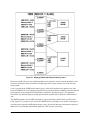
5. Memory Management
5.1 Overview...................................................... 54
5.1.1 Block Diagram .................................... 57
5.1.2 Registers .............................................. 58
5.2 Dependencies ............................................... 60
5.2.1 I/O Pins ................................................ 60
5.2.2 Clocks .................................................. 60
5.2.3 Interrupts ............................................. 60
5.3 Operation...................................................... 61
5.3.1 Internal RAM ...................................... 61
5.3.2 Memory Management Unit (MMU) ... 61
5.3.3 Memory Bank Operation ..................... 62
5.3.4 Memory Modes ................................... 64
5.3.5 Separate Instruction and Data Space ... 66
5.3.6 Memory Protection .............................. 67
5.3.7 Stack Protection .................................. 67
5.4 Register Descriptions ................................... 68
2. Clocks
2.1 Overview ......................................................16
2.1.1 Block Diagram .....................................17
2.1.2 Registers ..............................................17
2.2 Dependencies ...............................................18
2.2.1 I/O Pins ................................................18
2.2.2 Other Registers ....................................19
2.3 Operation ......................................................20
2.3.1 Main Clock ..........................................20
2.3.2 Main PLL .............................................21
2.3.3 Spectrum Spreader ...............................22
2.3.4 Clock Doubler .....................................24
2.3.5 32 kHz Clock .......................................26
2.4 Register Descriptions ...................................28
3. Reset and Bootstrap
3.1 Overview ......................................................35
3.1.1 Block Diagram .....................................36
3.1.2 Registers ..............................................36
3.2 Dependencies ...............................................37
3.2.1 I/O Pins ................................................37
3.2.2 Clocks ..................................................37
3.2.3 Other Registers ....................................37
3.2.4 Interrupts ..............................................37
3.3 Operation ......................................................38
3.3.1 Asynchronous Serial Bootstrap ...........40
3.3.2 Serial Flash Bootstrap ..........................40
3.3.3 Parallel Bootstrap ................................41
3.4 Register Descriptions ...................................41
6. Interrupts
6.1 Overview...................................................... 83
6.2 Operation...................................................... 84
6.3 Interrupt Tables ............................................ 84
7. External Interrupts
7.1 Overview...................................................... 87
7.2 Block Diagram ............................................. 88
7.2.1 Registers ............................................. 89
7.3 Dependencies ............................................... 90
7.3.1 I/O Pins ................................................ 90
7.3.2 Clocks .................................................. 90
7.3.3 Interrupts ............................................. 90
7.4 Operation...................................................... 91
7.4.1 Example ISR ....................................... 91
7.5 Register Descriptions ................................... 92
4. System Management
4.1 Overview ......................................................42
4.1.1 Block Diagram .....................................43
4.1.2 Registers ..............................................44
4.2 Dependencies ...............................................45
4.2.1 I/O Pins ................................................45
4.2.2 Clocks ..................................................45
4.2.3 Interrupts ..............................................45
4.3 Operation ......................................................46
4.3.1 Periodic Interrupt .................................46
Rabbit 6000 User’s Manual
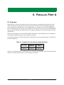
8. Parallel Port A
digi.com
8.1 Overview...................................................... 94
8.1.1 Block Diagram .................................... 95
8.1.2 Registers .............................................. 95
8.2 Dependencies ............................................... 96
8.2.1 I/O Pins ................................................ 96
3
8.2.2 Clocks ..................................................96
8.2.3 Other Registers ....................................96
8.2.4 Interrupts .............................................96
8.3 Operation......................................................97
8.4 Register Descriptions ...................................98
9. Parallel Port B
9.1 Overview ....................................................100
9.1.1 Block Diagram ..................................101
9.1.2 Registers ............................................102
9.2 Dependencies .............................................102
9.2.1 I/O Pins ..............................................102
9.2.2 Clocks ................................................102
9.2.3 Other Registers ..................................102
9.2.4 Interrupts ...........................................102
9.3 Operation....................................................103
9.4 Register Descriptions .................................104
10. Parallel Port C
10.1 Overview ..................................................106
10.1.1 Block Diagram ................................107
10.1.2 Registers ..........................................108
10.2 Dependencies ...........................................108
10.2.1 I/O Pins ............................................108
10.2.2 Clocks ..............................................108
10.2.3 Other Registers ................................108
10.2.4 Interrupts .........................................108
10.3 Operation..................................................109
10.4 Register Descriptions ...............................110
11. Parallel Port D
11.1 Overview ..................................................113
11.1.1 Block Diagram ................................115
11.1.2 Registers ..........................................116
11.2 Dependencies ...........................................117
11.2.1 I/O Pins ............................................117
11.2.2 Clocks ..............................................117
11.2.3 Other Registers ................................117
11.2.4 Interrupts .........................................117
11.3 Operation..................................................118
11.4 Register Descriptions ...............................119
12. Parallel Port E
12.1 Overview ..................................................125
12.1.1 Block Diagram ................................127
12.1.2 Registers ..........................................128
12.2 Dependencies ...........................................129
12.2.1 I/O Pins ............................................129
12.2.2 Clocks ..............................................129
12.2.3 Other Registers ................................129
12.2.4 Interrupts .........................................129
12.3 Operation..................................................130
12.4 Register Descriptions ...............................131
13. Parallel Port F
13.1 Overview ..................................................136
13.1.1 Block Diagram ................................138
Rabbit 6000 User’s Manual
digi.com
13.1.2 Registers .......................................... 139
13.2 Dependencies ........................................... 139
13.2.1 I/O Pins ............................................ 139
13.2.2 Clocks .............................................. 139
13.2.3 Other Registers ................................ 139
13.2.4 Interrupts ......................................... 140
13.3 Operation.................................................. 140
13.4 Register Descriptions ............................... 141
14. Parallel Port G
14.1 Overview.................................................. 145
14.1.1 Block Diagram ................................ 146
14.1.2 Registers .......................................... 147
14.2 Dependencies ........................................... 147
14.2.1 I/O Pins ............................................ 147
14.2.2 Clocks .............................................. 147
14.2.3 Other Registers ................................ 147
14.2.4 Interrupts ......................................... 148
14.3 Operation.................................................. 148
14.4 Register Descriptions ............................... 149
15. Parallel Port H
15.1 Overview.................................................. 153
15.1.1 Block Diagram ................................ 154
15.1.2 Registers .......................................... 155
15.2 Dependencies ........................................... 156
15.2.1 I/O Pins ............................................ 156
15.2.2 Clocks .............................................. 156
15.2.3 Other Registers ................................ 156
15.2.4 Interrupts ......................................... 156
15.3 Operation.................................................. 157
15.4 Register Descriptions ............................... 158
16. Timer A
16.1 Overview.................................................. 161
16.1.1 Block Diagram ................................ 163
16.1.2 Registers .......................................... 164
16.2 Dependencies ........................................... 165
16.2.1 I/O Pins ............................................ 165
16.2.2 Clocks .............................................. 165
16.2.3 Other Registers ................................ 165
16.2.4 Interrupts ......................................... 165
16.3 Operation.................................................. 166
16.3.1 Handling Interrupts ......................... 166
16.3.2 Example ISR ................................... 166
16.4 Register Descriptions ............................... 167
17. Timer B
17.1 Overview.................................................. 169
17.1.1 Block Diagram ................................ 170
17.1.2 Registers .......................................... 171
17.2 Dependencies ........................................... 171
17.2.1 I/O Pins ............................................ 171
17.2.2 Clocks .............................................. 171
17.2.3 Other Registers ................................ 171
17.2.4 Interrupts ......................................... 172
17.3 Operation.................................................. 172
17.3.1 Handling Interrupts ......................... 172
4
17.3.2 Example ISR ....................................172
17.4 Register Descriptions ...............................173
18. Timer C
18.1 Overview ..................................................176
18.1.1 Block Diagram ................................177
18.1.2 Registers ..........................................178
18.2 Dependencies ...........................................179
18.2.1 I/O Pins ............................................179
18.2.2 Clocks ..............................................179
18.2.3 Other Registers ................................179
18.2.4 Interrupts .........................................179
18.3 Operation..................................................180
18.3.1 Handling Interrupts ..........................180
18.3.2 Example ISR ....................................180
18.4 Register Descriptions ...............................181
19. Serial Ports A – D
19.1 Overview ..................................................184
19.1.1 Block Diagram ................................186
19.1.2 Registers ..........................................187
19.2 Dependencies ...........................................188
19.2.1 I/O Pins ............................................188
19.2.2 Clocks ..............................................188
19.2.3 Other Registers ................................189
19.2.4 Interrupts .........................................189
19.3 Operation..................................................190
19.3.1 Asynchronous Mode ........................190
19.3.2 Clocked Serial Mode .......................191
19.4 Register Descriptions ...............................193
20. Serial Ports E – F
20.1 Overview ..................................................200
20.1.1 Block Diagram ................................201
20.1.2 Registers ..........................................202
20.2 Dependencies ...........................................203
20.2.1 I/O Pins ............................................203
20.2.2 Clocks ..............................................203
20.2.3 Other Registers ................................203
20.2.4 Interrupts .........................................204
20.3 Operation..................................................205
20.3.1 Asynchronous Mode ........................205
20.3.2 HDLC Mode ....................................205
20.3.3 More on Clock Synchronization and
Data Encoding ...........................................206
20.4 Register Descriptions ...............................210
21. Slave Port
21.1 Overview ..................................................216
21.1.1 Block Diagram ................................217
21.1.2 Registers ..........................................217
21.2 Dependencies ...........................................218
21.2.1 I/O Pins ............................................218
21.2.2 Clocks ..............................................218
21.2.3 Interrupts .........................................218
21.3 Operation..................................................219
21.3.1 Master Setup ....................................220
21.3.2 Slave Setup ......................................220
21.3.3 Master/Slave Communication .........221
Rabbit 6000 User’s Manual
digi.com
21.3.4 Slave/Master Communication ......... 221
21.3.5 Handling Interrupts ......................... 221
21.3.6 Example ISR ................................... 221
21.3.7 Other Configurations ....................... 222
21.3.8 Timing Diagrams ............................ 223
21.4 Register Descriptions ............................... 225
22. Wi-Fi Analog Components
22.1 Overview.................................................. 227
22.2 Block Diagram ......................................... 230
22.2.1 Registers .......................................... 231
22.3 Dependencies ........................................... 231
22.3.1 I/O Pins ............................................ 231
22.3.2 Clocks .............................................. 231
22.4 Operation.................................................. 232
22.4.1 Fast A/D Converter ......................... 232
22.4.2 Fast D/A Converter ......................... 232
22.4.3 Slow A/D Converter ........................ 232
22.5 Sample Circuits........................................ 233
22.6 Register Descriptions ............................... 235
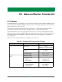
23. Analog/Digital Converter
23.1 Overview.................................................. 240
23.2 Block Diagram ......................................... 241
23.2.1 Registers .......................................... 241
23.3 Dependencies ........................................... 242
23.3.1 I/O Pins ............................................ 242
23.3.2 Clocks .............................................. 242
23.4 Operation.................................................. 243
23.4.1 Single Reading ................................ 243
23.4.2 Continuous Read ............................. 243
23.4.3 Handling Interrupts ......................... 243
23.5 Sample Circuit ......................................... 244
23.6 Register Descriptions ............................... 245
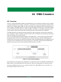
24. DMA Channels
24.1 Overview.................................................. 249
24.1.1 Block Diagram ................................ 252
24.1.2 Registers .......................................... 253
24.2 Dependencies ........................................... 255
24.2.1 I/O Pins ............................................ 255
24.2.2 Clocks .............................................. 255
24.2.3 Other Registers ................................ 255
24.2.4 Interrupts ......................................... 255
24.3 Operation.................................................. 256
24.3.1 Handling Interrupts ......................... 257
24.3.2 Example ISR ................................... 257
24.3.3 DMA Priority with the Processor .... 258
24.3.4 DMA Channel Priority .................... 259
24.3.5 Buffer Descriptor Modes ................. 260
24.3.6 DMA with Peripherals .................... 263
24.4 Register Descriptions ............................... 264
25. 10/100Base-T Ethernet
25.1 Overview.................................................. 285
25.1.1 Block Diagram ................................ 287
25.1.2 Registers .......................................... 288
25.2 Dependencies ........................................... 290
5
25.2.1 I/O Pins ............................................290
25.2.2 Clocks ..............................................290
25.2.3 Other Registers ................................290
25.2.4 Interrupts .........................................291
25.3 Operation..................................................291
25.3.1 Setup ................................................291
25.3.2 Transmit ...........................................292
25.3.3 Receive ............................................292
25.3.4 Handling Interrupts ..........................293
25.3.5 Multicast Addressing .......................294
25.4 Register Descriptions ...............................295
29.1.2 Registers .......................................... 335
29.2 Dependencies ........................................... 336
29.2.1 I/O Pins ............................................ 336
29.2.2 Clocks .............................................. 336
29.2.3 Other Registers ................................ 336
29.2.4 Interrupts ......................................... 336
29.3 Operation.................................................. 337
29.3.1 Handling Interrupts ......................... 337
29.3.2 Example ISR ................................... 337
29.4 Register Descriptions ............................... 338
30. Pulse Width Modulator
26. 802.11a/b/g Wireless
26.1 Overview ..................................................309
26.1.1 Block Diagram ................................310
26.1.2 Registers ..........................................311
26.2 Dependencies ...........................................313
26.2.1 I/O Pins ............................................313
26.3 Clocks.......................................................314
26.3.1 Other Registers ................................315
26.3.2 Interrupts .........................................316
26.4 Operation..................................................316
27. USB Host
27.1 Overview ..................................................317
27.1.1 Block Diagram ................................317
27.1.2 Registers ..........................................318
27.2 Dependencies ...........................................318
27.2.1 I/O Pins ............................................318
27.2.2 Clocks ..............................................318
27.2.3 Other Registers ................................319
27.2.4 Interrupts .........................................319
27.3 Operation..................................................320
27.3.1 32-bit Interface ................................320
27.3.2 Setup ................................................320
27.3.3 Transmit and Receive ......................320
27.3.4 Handling Interrupts ..........................320
27.4 Register Descriptions ...............................321
28. Input Capture
28.1 Overview ..................................................322
28.1.1 Block Diagram ................................323
28.1.2 Registers ..........................................324
28.2 Dependencies ...........................................325
28.2.1 I/O Pins ............................................325
28.2.2 Clocks ..............................................325
28.2.3 Other Registers ................................325
28.2.4 Interrupts .........................................325
28.3 Operation..................................................326
28.3.1 Input-Capture Channel ....................326
28.3.2 Handling Interrupts ..........................326
28.3.3 Example ISR ....................................326
28.3.4 Capture Mode ..................................327
28.3.5 Count Mode .....................................327
28.4 Register Descriptions ...............................328
30.1 Overview.................................................. 340
30.1.1 Block Diagram ................................ 343
30.1.2 Registers .......................................... 343
30.2 Dependencies ........................................... 344
30.2.1 I/O Pins ............................................ 344
30.2.2 Clocks .............................................. 344
30.2.3 Other Registers ................................ 344
30.2.4 Interrupts ......................................... 344
30.3 Operation.................................................. 345
30.3.1 Handling Interrupts ......................... 345
30.3.2 Example ISR ................................... 345
30.4 Register Descriptions ............................... 346
31. External I/O Control
31.1 Overview.................................................. 348
31.1.1 External I/O Bus .............................. 348
31.1.2 I/O Strobes ...................................... 349
31.1.3 I/O Handshake ................................. 350
31.1.4 Block Diagram ................................ 351
31.1.5 Registers .......................................... 352
31.2 Dependencies ........................................... 353
31.2.1 I/O Pins ............................................ 353
31.2.2 Clocks .............................................. 353
31.2.3 Other Registers ................................ 353
31.2.4 Interrupts ......................................... 353
31.3 Operation.................................................. 354
31.3.1 External I/O Bus .............................. 354
31.3.2 I/O Strobes ...................................... 354
31.3.3 I/O Handshake ................................. 354
31.4 Register Descriptions ............................... 355
32. Breakpoints
32.1 Overview.................................................. 360
32.1.1 Block Diagram ................................ 361
32.1.2 Registers .......................................... 362
32.2 Dependencies ........................................... 363
32.2.1 I/O Pins ............................................ 363
32.2.2 Clocks .............................................. 363
32.2.3 Other Registers ................................ 363
32.2.4 Interrupts ......................................... 363
32.3 Operation.................................................. 363
32.3.1 Handling Interrupts ......................... 363
32.3.2 Example ISR ................................... 364
32.4 Register Descriptions ............................... 365
29. Quadrature Decoder
29.1 Overview ..................................................333
29.1.1 Block Diagram ................................335
Rabbit 6000 User’s Manual
digi.com
33. Flexible Interface Modules
33.1 Overview.................................................. 368
6
33.2 Block Diagram .........................................369
33.2.1 Registers ..........................................370
33.3 Dependencies ...........................................371
33.3.1 I/O Pins ............................................371
33.3.2 Clocks ..............................................371
33.3.3 Other Registers ................................371
33.3.4 Interrupts .........................................371
33.4 Operation..................................................372
33.4.1 Handling Interrupts ..........................372
33.5 Register Descriptions ...............................374
37.3.2 Memory Writes ............................... 419
37.3.3 External I/O Reads .......................... 422
37.3.4 External I/O Writes ......................... 422
37.4 Clock Speeds............................................ 425
37.4.1 Recommended Clock/Memory
Configurations .......................................... 425
37.5 Power and Current Consumption............. 427
37.5.1 Sleepy Mode Current Consumption 427
37.5.2 Battery-Backed Clock Current
Consumption ............................................. 428
38. Package Specifications and Pinout
34. Error Check and Correction
34.1 Overview ..................................................383
34.1.1 Block Diagram ................................384
34.1.2 Registers ..........................................384
34.2 Dependencies ...........................................385
34.2.1 I/O Pins ............................................385
34.2.2 Clocks ..............................................385
34.2.3 Other Registers ................................385
34.3 Operation..................................................385
34.3.1 ECC .................................................385
34.3.2 CRC .................................................385
34.4 Register Descriptions ...............................386
38.1 Ball Grid Array Packages ........................ 429
38.1.1 Pinout 17mm × 17mm BGA 292 .... 429
38.1.2 Pinout 15mm × 15mm BGA 233 .... 430
38.1.3 Mechanical Dimensions and Land
Pattern ....................................................... 431
38.2 Rabbit Pin Descriptions ........................... 434
Appendix A. Parallel Port Pins with
Alternate Functions
A.1 Alternate Parallel Port Pin Outputs........... 441
A.2 Alternate Parallel Port Pin Inputs.............. 444
35. I2C Peripheral (Serial Port G)
35.1 Overview ..................................................389
35.1.1 Block Diagram ................................390
35.1.2 Registers ..........................................391
35.2 Dependencies ...........................................392
35.2.1 I/O Pins ............................................392
35.2.2 Clocks ..............................................392
35.2.3 Other Registers ................................392
35.2.4 Interrupts .........................................392
35.3 Operation..................................................393
35.3.1 32-bit Interface ................................393
35.3.2 Interrupts .........................................393
35.3.3 Master Mode, Data Write ................393
35.3.4 Master Mode, Data Read .................394
35.3.5 Slave Mode, Data Write ..................394
35.3.6 Slave Mode, Data Read ...................394
35.4 Register Descriptions ...............................395
36. Low-Power Operation
36.1 Overview ..................................................403
36.1.1 Registers ..........................................404
36.2 Operation..................................................405
36.2.1 Unused Pins .....................................405
36.2.2 Unused Peripherals ..........................405
36.2.3 Clock Rates ......................................405
36.2.4 Short Chip Selects ...........................407
36.2.5 Self-Timed Chip Selects ..................412
36.3 Register Descriptions ...............................413
37. Specifications
37.1 Preliminary DC Characteristics................416
37.2 AC Characteristics ...................................418
37.3 External Memory Access Times ..............419
37.3.1 Memory Reads ................................419
Rabbit 6000 User’s Manual
digi.com
7
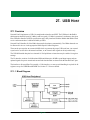
1. THE RABBIT 6000 PROCESSOR
1.1 Introduction
Rabbit Semiconductor was formed expressly to design a better microprocessor for use in small- and
medium-scale, single-board computers. The first microprocessors were the Rabbit 2000, Rabbit 3000, Rabbit 4000, and the Rabbit 5000. The latest microprocessor is the Rabbit 6000. Rabbit microprocessor
designers have had years of experience using Z80, Z180, and HD64180 microprocessors in small singleboard computers. The Rabbit microprocessors share a similar architecture and a high degree of compatibility with these microprocessors, but represent a vast improvement.
The Rabbit 6000 is a high-performance microprocessor with low electromagnetic interference (EMI), and
is designed specifically for embedded control, communications, and network connectivity. Extensive integrated features and glueless architecture facilitate rapid hardware design, while a C-friendly instruction set
promotes efficient development of even the most complex applications.
The Rabbit 6000 is the second Rabbit microprocessor to have a full 16-bit internal bus architecture, providing significant performance improvements when used with external 16-bit memory devices. It also has
the ability to support both 8-bit and 16-bit external memory devices.
The Rabbit 6000 is also the fastest microprocessor from Rabbit, now a Digi International brand, running at
up to 200 MHz, with compact code and support for up to 16 MB of memory. Operating with a 1.2 V core
and 3.3 V I/O, the Rabbit 6000 boasts 16 channels of DMA, six serial ports with IrDA, 64+ digital I/O,
quadrature decoder, PWM outputs, I2C port, and pulse capture and measurement capabilities. It also features a battery-backable real-time clock, glueless memory and I/O interfacing, and ultra-low power modes.
Four levels of interrupt priority allow fast response to real-time events. Its compact instruction set and high
clock speeds give the Rabbit 6000 exceptionally fast math, logic, and I/O performance.
The Rabbit 6000 contains 1MB of internal high-speed 16-bit RAM, which can be used for both code and
data. It also contains 32 KB of battery-backable 16-bit SRAM (also high speed) for applications where
data retention is critical. It is capable of booting off of a standard serial flash, so a microcontroller application with no external parallel memory is possible.
The Rabbit 6000 provides two options for network connectivity — a full 10/100Base-T Ethernet MAC and
PHY built into the device, and a wireless 802.11a/b/g MAC compatible with several standard Wi-Fi transceivers. Both network interfaces can be active at the same time. The Rabbit 6000 also contains a USB 2.0compatible full-speed USB host MAC and PHY.
The Rabbit 6000 also features two “flexible interface modules,” or FIMs. These two modules can be
loaded with customized designs to support a variety of interfaces, including serial ports and CAN-bus
interfaces.
Rabbit 6000 User’s Manual
digi.com
8
1.2 Features
The Rabbit 6000 contains an internal phase-locked loop (PLL) that is fully controlled by software and provides up to a 200 MHz clock from a 25 MHz input. Other clock options are available as well, including the
clock doubler and divider features present in earlier Rabbit devices.
The Rabbit 6000 has several powerful design features that practically eliminate EMI problems, which is
essential for OEMs who need to pass CE and regulatory radio-frequency emissions tests. The amplitude of
any electromagnetic radiation is reduced by the internal spectrum spreader, by gated clocks (which prevent
unnecessary clocking of unused registers), and by separate power planes for the processor core and I/O
pins (which reduce noise crosstalk). An external I/O bus can be used by designers to enable separate buses
for I/O and memory, or to limit loading the memory bus to reduce EMI and ground bounce problems when
interfacing external peripherals to the processor. The external I/O bus accomplishes this by duplicating the
Rabbit's data bus on Parallel Port A, and uses Parallel Port B to provide the processor's six or eight least
significant address lines for interfacing with external peripherals.
The high-performance instruction set offers both greater efficiency and execution speed of compiler-generated C code. Instructions include numerous single-byte opcodes that execute in two clock cycles, 16-bit and
32-bit loads and stores, 16-bit and 32-bit logical and arithmetic operations, 16 × 16 multiply (executes in
12 clocks), long jumps and returns for accessing a full 16 MB of memory, and one-byte prefixes to turn
memory-access instructions into internal and external I/O instructions. Hardware-supported breakpoints
ease debugging by trapping on code execution or data reads and writes.
The Rabbit 6000 requires no external memory driver or interface logic. Its 24-bit address bus, 8-bit or 16bit data bus, three chip-select lines, two output-enable lines, and two write-enable lines can be interfaced
directly with up to six memory devices. Up to 1 MB of code memory and 15 MB of data memory can be
accessed directly via the Dynamic C development software. The Rabbit 6000 also contains 1 MB of internal high-speed 16-bit RAM and 32 KB of battery-backed SRAM, which can be used instead of or in addition to any external memory devices.
A built-in slave port allows the Rabbit 6000 to be used as master or slave in multi-processor systems, permitting separate tasks to be assigned to dedicated processors. An 8-line data port and five control signals
simplify the exchange of data between devices. A remote cold boot enables startup and programming via a
serial port, a slave port, or from a standard external serial flash device.
The Rabbit 6000 features eight 8-bit parallel ports, yielding a total of 64 digital I/O. Six CMOS-compatible serial ports are available. All six are configurable as asynchronous (including output pulses in IrDA
format), while four are configurable as clocked serial (SPI) and two are configurable as SDLC/HDLC. The
various internal peripherals share the parallel port’s I/O pins. Drive strength, slew rate, and pullup/pulldown resistors can be controlled on all of the parallel ports.
The Rabbit 6000 also offers many specialized peripherals. Two input-capture channels each have a 16-bit
counter, clocked by the output of an internal timer, that can be used to capture and measure pulses. These
measurements can be extended to a variety of functions such as measuring pulse widths or for baud-rate
auto detection. Two Quadrature Decoder channels each have two inputs, as well as an 8-bit or 10-bit up/
down counter. Each Quadrature Decoder channel provides a direct interface to quadrature encoder units.
Four independent pulse-width modulator (PWM) outputs, each based on a 1024-pulse frame, are driven by
the output of a programmable internal timer. The PWM outputs can be filtered to create a 10-bit D/A converter or they can be used directly to drive devices such as motors or solenoids. The Rabbit 6000 has eight
Rabbit 6000 User’s Manual
digi.com
9
external interrupt vectors, two of which can each multiplex inputs from up to three external pins. A new
addition to the Rabbit 6000 is a fully featured I2C port capable of up to 400 kbits/s and 10-bit addressing.
The Rabbit 6000 has three timer systems. Timer A consists of twelve 8-bit counters, each of which has a programmed time constant. Six of them can be cascaded from the primary Timer A counter. Timer B contains a
10-bit counter, two match registers, and two step registers. An interrupt can be generated or an output pin
can be updated when the counter reaches a match value, and the match value can then be incremented automatically by the step value. Timer C is a 16-bit counter that counts up to a programmable limit. It contains
eight match registers so that up to four PWM (both synchronous and variable-phase) or quadrature signals
for motor-control applications can be created.
The Rabbit 6000 also provides support for protected operating systems. Support for two levels of operation, known as system and user modes, allow application-critical code to operate in safety while user code
is prevented from inadvertently disturbing the setup of the processor. Memory blocks as small as 4 KB can
be write-protected against accidental writes by user code, and stack over/underflows can be trapped by
high-priority interrupts.
Security features are also available in the Rabbit 6000. New instructions were added to the existing
encryption support to increase encryption algorithm speeds dramatically, and 32 bytes of battery-backed
RAM can store an encryption key away from prying eyes.
The Rabbit 6000 supports sixteen channels of DMA access to internal or external memory, internal I/O
addresses, and the external I/O bus. Directing a DMA channel to or from an internal peripheral such as a
serial port or the Ethernet port automatically connects DMA enable signals. Burst size, priority, and guaranteed cycles for the processor are all under program control. DMA operations to/from the internal memory and peripherals can operate simultaneously with code fetches, so no performance hit occurs. When
accessing external memory, DMA operations will alternate between DMA and code fetches as in previous
Rabbit designs.
The Rabbit 6000 contains an 802.11a/b/g wireless MAC peripheral, also designed to operate with the DMA
peripheral. It includes support for all standard Wi-Fi features, including infrastructure and ad-hoc modes.
The high-speed internal A/D converter and D/A converter and clocked-serial control port provide a
generic interface to several common Wi-Fi transceivers. A low-speed A/D converter is also available to
monitor the transmit signal strength if desired. The two A/D converters and single D/A converter are available for customer use when the Wi-Fi peripheral is disabled.
The Rabbit 6000 also contains a full-featured 10/100Base-T Ethernet MAC peripheral and PHY. Designed
to operate with the DMA peripheral, the Ethernet peripheral is fully compliant with the 802.3 Ethernet
standard, including support for auto-negotiation, link detection, multicast filtering, and broadcast
addresses.
The Rabbit 6000 provides an Open Host Controller Interface (OHCI) USB device MAC and PHY. Fully
supported by the DMA peripheral, the MAC and PHY are USB 2.0 compliant, full-speed (12 Mbit/s)
devices.
Another new feature of the Rabbit 6000 is a 12-bit, 8-channel A/D converter. This A/D converter can run
at up to 1 megasample per second, based on either the internal clock or an external clock input. The A/D
converter is muxed across eight channels which can be sampled individually or continuously across all
channels.
Rabbit 6000 User’s Manual
digi.com
10
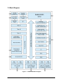
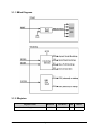
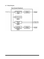
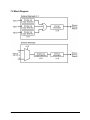
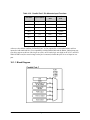
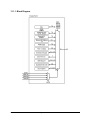
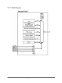
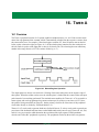
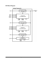
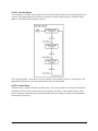
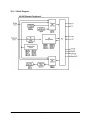
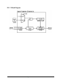
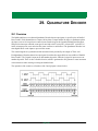
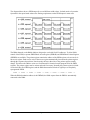
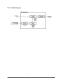
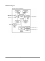
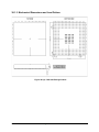
1.3 Block Diagram
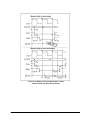
Figure 1.1 Rabbit 6000 Block Diagram
Rabbit 6000 User’s Manual
digi.com
11
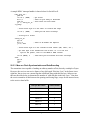
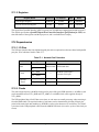
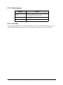
1.4 Basic Specifications
Two versions of the Rabbit 6000 are available—the standard 292-ball BGA and a smaller 233-ball BGA
for specialty Wi-Fi applications. The larger package is intended for most Rabbit applications; the smaller
package has no address or data bus, and is intended for particular applications. If you need further information, please contact your Rabbit sales representative.
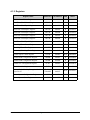
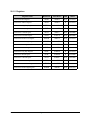
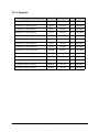
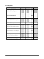
Table 1-1. Rabbit 6000 Specifications and Features
Package
Package Size
292-ball BGA
233-ball BGA
17 mm × 17 mm × 1.3 mm
15 mm × 15 mm × 1.3 mm
Operating Voltage
Operating Current (typ)
1.2 V DC core, 3.3 V DC I/O ring
372 A/MHz @ 1.2 V/3.3 V, 25-200 MHz
(Wi-Fi and Ethernet disabled)
Operating Temp.
-40°C to +85°C
Maximum Clock Speed
200 MHz
Digital I/O
64+ (arranged in
eight 8-bit ports)
Network Interfaces
10/100Base-T
802.11b/g Wi-Fi
Serial Ports
6 CMOS-compatible
Baud Rate
I2C Ports
2 CMOS-compatible
Clock speed/8 max. asynchronous
1
1
24-bit
None
Data Bus
8/16-bit
None
Timers
Twelve 8-bit, one 10-bit with 2 match registers,
and one 16-bit with 8 match registers
Address Bus
Real-Time Clock
Yes, battery-backable
RTC Oscillator Circuitry
External
Watchdog Timer/Supervisor
Yes
1×, 2×, /2, /3, /4, /6, /8*
Clock Modes
Sleepy (32 kHz)
Ultra-Sleepy (16, 8, 4, 2 kHz)*
Power-Down Modes
External I/O Bus
8 data, 8 address lines
No
A/D Converters
10-bit, 2 synchronous channels, up to 40 megasamples/s
10-bit, single channel, up to 1 megasamples/s
12-bit, eight multiplexed channels, up to 1 megasamples/s
D/A Converters
10-bit, 2 synchronous channels, up to 80 megasamples/s
* Limitations on the use of the 1MB internal RAM are present when running in lower CPU frequency or
sleepy modes. See Section 5.3.1, “Internal RAM”.
Rabbit 6000 User’s Manual
digi.com
12
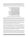
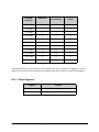
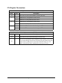
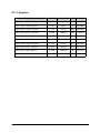
1.5 Comparing Rabbit Microprocessors
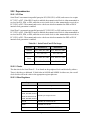
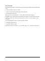
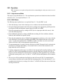
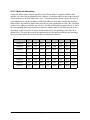
The Rabbit 2000, Rabbit 3000, Rabbit 4000, Rabbit 5000, and Rabbit 6000 features are compared below.
Feature
Rabbit 6000
Rabbit 5000
Rabbit 4000
Rabbit 3000
Rabbit 2000
Maximum Clock Speed,
industrial
200 MHz
100 MHz
60 MHz
55.5 MHz
30 MHz
Maximum Clock Speed,
commercial
200 MHz
100 MHz
60 MHz
58.8 MHz
30 MHz
Maximum Crystal Frequency 24–42 MHz
(crystal)
Main Oscillator (may be
increased internally up to
20–200 MHz
maximum clock speed)
(ext. clock)
100 MHz
60 MHz
30 MHz
30 MHz
32.768 kHz Crystal
Oscillator
External
External
External
External
Internal
Operating Voltage, core
1.2 V ± 10%
1.8 V ± 10%
1.8 V ± 10%
Operation Voltage, I/O
1.2 V ± 10%
3.3 V ± 10%
1.8 V ± 10%
3.3 V ± 10%
1.8 V ± 10%
3.3 V ± 10%
3.3 V ± 10%
5.0 V ± 10%
3.6 V
3.6 V
3.6 V
5.5 V
5.5 V
2 mA/MHz
@ 3.3 V
4 mA/MHz
@5V
128
128
100
16 × 16 × 1.5
mm
16 × 16 × 1.5
mm
24 × 18 × 3
mm
0.4 mm
(16 mils)
0.4 mm
(16 mils)
0.65 mm
(26 mils)
Maximum I/O Input Voltage
Current Consumption
(32kHz – 200MHz)
Number of Package Pins
0.37 mA/MHz 0.57 mA/MHz
@ 1.2 V/3.3 V @ 1.8 V/3.3 V
0.35 mA/MHz
(Wi-Fi and
(Wi-Fi and
@ 3.3 V
Ethernet
Ethernet
disabled)
disabled)
292/233
Size of Package, LQFP/
PQFP
289/196
N/A
Spacing Between
Package Pins
17 × 17 × 1.3
15 × 15 × 1.4
10 × 10 × 1.2
10 × 10 × 1.2
0.8 mm
0.8 mm
0.8 mm
0.8 mm
Separate Power and
Ground for I/O Buffers
(EMI reduction)
Yes
Yes
Yes
Yes
No
Clock Spectrum Spreader
Yes
Yes
Yes
Yes
Rabbit 2000B/C
Yes, up to
200MHz
No
No
No
No
1×, 2×, /2, /3,
/4, /6, /8*
1×, 2×, /2, /3,
/4, /6, /8
1×, 2×, /2, /3,
/4, /6, /8
1x, 2x, /2, /3
/4, /6, /8
1x, 2x, /4, /8
Size of Package, BGA (mm)
Spacing Between
Package Pins
Phase-Locked Loop
Clock Modes
Rabbit 6000 User’s Manual
digi.com
N/A
13
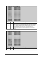
Feature
Powerdown Modes, sleepy
Powerdown Modes,
ultra sleepy
Rabbit 6000
Rabbit 5000
Rabbit 4000
Rabbit 3000
32 kHz
32 kHz
32 kHz
32 kHz
Rabbit 2000
32 kHz
16, 8, 4, 2 kHz* 16, 8, 4, 2 kHz 16, 8, 4, 2 kHz 16, 8, 4, 2 kHz
Short and
Self-Timed
Chip Selects
Short and
Self-Timed
Chip Selects
Short and
Self-Timed
Chip Selects
Short and
Self-Timed
Chip Selects
None
Yes
Yes
Yes
Yes
No
24 bits
20–24 bits
20–24 bits
20 bits
20 bits
External Data Bus Size
8/16 bits
8/16 bits
8/16 bits
8 bits
8 bits
Internal Data Bus Size
16 bits
16 bits
8 bits
8 bits
8 bits
1 MB + 32KB
battery-backed
128KB
None
None
None
8
6
5
7
5
Yes
Yes
Yes
Yes
None
Number of Serial Ports
6
6
6
6
4
DMA Channels
16
8
8
None
None
Low-Power Memory Control
Extended Memory Timing
for High-Frequency
Operation
Address Bus Size
Internal RAM
Number of 8-bit I/O Ports
External I/O
Data/Address Bus
Serial Ports Capable of
SPI/Clocked Serial
Serial Ports Capable of
SDLC/HDLC
Asynch Serial Ports With
Support for
IrDA Communication
Serial Ports with Support for
SDLC/HDLC IrDA
Communication
Serial Ports with 4-Byte
FIFO
Maximum Asynchronous
Baud Rate
Hardware I2C Ports
Ethernet Port
Wi-Fi (802.11a/b/g)
USB (2.0 compatible)
PWM Outputs
Rabbit 6000 User’s Manual
4 (A, B, C, D) 4 (A, B, C, D) 4 (A, B, C, D) 4 (A, B, C, D)
2 (A, B)
2 (E, F)
2 (E, F)
2 (E, F)
2 (E, F)
None
6
6
6
6
None
2 (E,F)
2 (E,F)
2 (E,F)
2 (E,F)
None
6
2 (E,F)
2 (E,F)
2 (E,F)
None
Clock speed/8 Clock Speed/8 Clock Speed/8 Clock Speed/8 Clock Speed/32
1
None
10/100Base-T 10/100Base-T
with PHY
(MAC only)
None
None
None
10Base-T
(partial PHY)
None
None
Yes
Yes
No
No
No
Full-speed host
No
No
No
No
4
4
4
4
None
digi.com
14
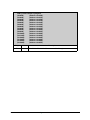
Feature
Rabbit 6000
Rabbit 5000
Rabbit 4000
Rabbit 3000
Rabbit 2000
Variable-Phase
PWM Outputs (PPM)
4
4
4
None
None
Input Capture Units
2
2
2
2
None
22/8
6/2
6/2
4/2
4/2
2 channels
2 channels
2 channels
2 channels
None
Flexible Interface Modules
2
None
None
None
None
Hardware Breakpoints
7
7
7
None
None
User A/D
Converter Channels
8
None
None
None
None
A/D Converter Channels
(Wi-Fi disabled)
3
3
None
None
None
D/A Converter Channels
(Wi-Fi disabled)
2
2
None
None
None
External Interrupts/Vectors
Quadrature Decoders
* Limitations on the use of the 1MB internal RAM are present when running in lower CPU frequency or
sleepy modes. See Section 5.3.1, “Internal RAM”.
Rabbit 6000 User’s Manual
digi.com
15
2. CLOCKS
2.1 Overview
The Rabbit 6000 supports up to five separate clocks at once—the main clock, the 32 kHz clock, the 20
MHz Wi-Fi clock, the 25 MHz Ethernet clock, and the 48 MHz USB clock. The main clock is used to
drive the processor clock and the peripheral clock inside the processor. The 32 kHz clock is used to drive
the asynchronous serial bootstrap, the real-time clock, the periodic interrupt, and the watchdog timers.
The 32 kHz clock input requires an external clock signal; the remaining clock inputs have internal oscillators that can be driven with just an external crystal. If desired, each of the remaining clock inputs can also
be used with an external clock as well, bypassing the internal oscillator.
The Ethernet peripheral can be driven from the main clock instead of the PHY clock input, removing the
need for separate main and Ethernet clocks. When this feature is enabled, the main clock must be 25 MHz
for proper Ethernet operation.
The main clock can be fed into a phase-locked loop (PLL), generating CPU and peripheral clocks in the
range of 150–200 MHz, depending on the input clock and PLL settings. This clock can be further adjusted
by the clock divider if desired. Dividers exist for most peripherals to scale their clocks over a wide range
of frequencies.
The Rabbit 6000 has a spectrum spreader on the main clock that shortens and lengthens clock cycles. This
has the net effect of reducing the peak energy of clock harmonics by spreading the spectral energy into
nearby frequencies, which reduces EMI and facilitates government-mandated EMI testing. Gated clocks
are used whenever possible to avoid clocking unused portions of the processor, and separate power-supply
pins for the core and I/O ring further reduce EMI from the Rabbit 6000. Note that the spectrum spreader is
not usable at main clock frequencies above 115 MHz because of the short period.
The main clock can be doubled or divided by 2, 4, 6, or 8 to reduce EMI and power consumption. The 32
kHz clock (which can be divided by 2, 4, 8, or 16) can be used instead of the main clock to generate processor and peripheral clocks as low as 2 kHz for significant power savings. Note that dividing the 32 kHz
clock only affects the processor and peripheral clocks; the full 32 kHz signal is still provided to the realtime clock and watchdog timer peripherals that use it directly. The periodic interrupt is disabled automatically since there is not enough time to process it when it is running off the 32 kHz clock. Also, note that
the internal RAM content will not be maintained at CPU frequencies below 12MHz.
There is also a 25 MHz Ethernet oscillator that connects directly to the Ethernet PHY if you are using the
Ethernet option, but want a different main clock frequency. See Chapter 25 for more details on the Ethernet clock.
The Wi-Fi peripheral requires a 20 MHz clock input, which goes to a dedicated PLL to produce the
required clocks for the 802.11a/b/g peripheral. The USB peripheral requires a 48 MHz clock for proper
operation.
Rabbit 6000 User’s Manual
digi.com
16
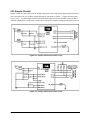
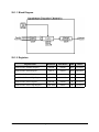
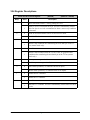
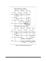
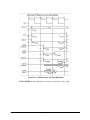
2.1.1 Block Diagram
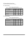
2.1.2 Registers
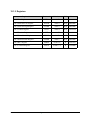
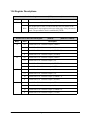
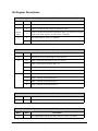
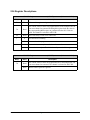
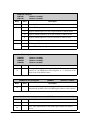
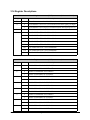
Register Name
Mnemonic
I/O Address
R/W
Reset
GCSR
0x0000
R/W
11000000
Global Clock Modulator 0 Register
GCM0R
0x000A
W
00000000
Global Clock Modulation 1 Register
GCM1R
0x000B
W
00000000
Global Clock Double Register
GCDR
0x000F
R/W
00000000
Master System Configuration Register
MSCR
0x0434
R/W
00000000
Master System Status Register
MSSR
0x0435
R/W
00000x00
Global Control/Status Register
Rabbit 6000 User’s Manual
digi.com
17
2.2 Dependencies
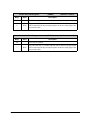
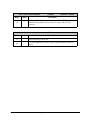
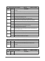
2.2.1 I/O Pins
The main, Wi-Fi, Ethernet, and USB clocks contain a bypassable internal oscillator, so either a crystal or an
external clock input can be used. The selection of a crystal or an external signal for the main oscillator is
determined by the state of the CFG pins on startup, and by the Master System Status Register (MSSR). The
Ethernet clock source (main clock or PHY oscillator) is selected in the Master System Configuration Register (MSCR). Table 2-1 lists the pins assigned to each clock and how they are controlled.
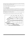
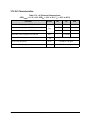
Table 2-1. Clock Pin Assignments
Frequency
Crystal Pins
External Clock
Signal Pins
Crystal/External
Clock Selection by
Main Clock
24 –42 MHz
(crystal)
20–200 MHz
(external
clock)
CLK_HSI
CLK_HSO
CLK_HSO
CFG pins
(see chapter 3)
W-Fi Clock
20 MHz
XTL_20MI
XTL_20MO
XTL_20MO
MSSR
Ethernet Clock
25 MHz
XTL_25MI
XTL_25MO
XTL_25MO
—
USB Clock
48 MHz
XTL_48MI
XTL_48MO
XTL_48MO
MSSR
32 kHz Clock
32 kHz
—
CLK_32K
—
Clock
The 32 kHz clock input is on the CLK_32K pin. There is an internal Schmitt trigger on this pin to reduce
sensitivity to noise.
The peripheral clock or peripheral clock divided by 2 may be optionally output on the CLK pin by
enabling it via bits 7–6 in GOCR.
Rabbit 6000 User’s Manual
digi.com
18
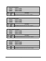
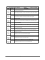
2.2.2 Other Registers
Register
Function
GOCR
Used to set up the CLK output pin.
MSCR
Used to:
- select clock input or PLL output for CPU clock
- select main clock or external 25 MHz clock for Ethernet
- select CPU clock or PLL output for Flexible Interface Modules
MSSR
Used to select crystal or external oscillator for Wi-Fi and USB clocks,
and read main and Wi-Fi PLL status.
GCM0R, GCM1R
Used to select the main PLL loop and pre-divider values.
GCDR
Used to enable the main PLL.
ENPR
Used to enable the Wi-Fi PLL (automatic when Wi-Fi is enabled).
Rabbit 6000 User’s Manual
digi.com
19
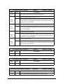
2.3 Operation
2.3.1 Main Clock
The main clock is based on the main oscillator output, which in turn is driven by the CLK_HSI and
CLK_HSO pins. This output serves as the input for the main PLL, which can be programmed for various
frequencies or bypassed completely. There is an option for the resulting output to then be sent through the
spectrum spreader and then the clock doubler, which are described later. This resulting clock is the main
clock.
Different main clock modes may be selected via the GCSR, as shown in Table 2-2. Note that one GCSR
setting slows the processor clock while the peripheral clock operates at full speed; this allows some power
reduction while keeping settings like serial baud rates and the PWM at their desired values.
Table 2-2. Clock Modes
GCSR Setting
Processor Clock
Peripheral Clock
xxx010xx
Main clock
Main clock
xxx011xx
Main clock / 2
Main clock / 2
xxx110xx
Main clock / 4
Main clock / 4
xxx111xx
Main clock / 6
Main clock / 6
xxx000xx
Main clock / 8
Main clock / 8 (default on startup)
xxx001xx
Main clock / 8
Main clock
xxx100xx
32 kHz clock (possibly divided)
32 kHz clock (possibly divided via
GPSCR)
xxx101xx
32 kHz clock (possibly divided);
main clock disabled via CLKIEN output
signal
32 kHz clock (possibly divided via
GPSCR)
When the 32 kHz clock is enabled in GCSR, it can be further divided by 2, 4, 8, or 16 to generate even
lower frequencies by enabling those modes in bits 0–2 of GPSCR. See Table 2-6 for more details.
Rabbit 6000 User’s Manual
digi.com
20
2.3.2 Main PLL
The main PLL is optimally tuned for a 25 MHz clock input and to produce a 400 MHz output, which can
be fed directly to the Flexible Interface Modules (FIMs), and is divided by two to 200 MHz for processor
and peripheral operation. Note that the main PLL can be bypassed if lower frequencies are desired.
The main PLL is enabled in GCDR, but is not selected as the main clock until enabled in MSCR. If the 32
kHz clock is present, then the switchover to the PLL output for the main clock will not occur until 200 µs
after the bit is enabled in MSCR to allow the PLL output to stabilize. The status of the main PLL (stable
output or not) can be read in bit 0 of MSSR.
The main PLL input clock is restricted to 20–200 MHz, and the output frequency range is limited to 300–
400 MHz. There are further restrictions on the internal frequency
The main PLL divider values are located in GCM0R and GCM1R. These should be set to a nonzero value
before enabling the PLL. Some suggested PLL settings are described in Table 2-3, chosen to match other
clock requirements in the design to allow clock sharing. If other PLL settings are desired, please contact
your sales representative at Digi International.
Table 2-3. Suggested PLL Modes
Input Clock
Main Clock
(max)
FIM Clock
(max)
GCM0R
Setting
GCM1R
Setting
20 MHz
150 MHz
300 MHz
xxx10000
xxxx0001
20 MHz
200 MHz
400 MHz
xxx10100
xxxx0001
25 MHz
150 MHz
300 MHz
xxx01100
xxxx0001
25 MHz
200 MHz
400 MHz
xxx10000
xxxx0001
48 MHz
156 MHz
312 MHz
xxx01101
xxxx0010
48 MHz
192 MHz
384 MHz
xxx10000
xxxx0010
Note that if the PLL is enabled, restrictions may exist for the use of the spectrum spreader and clock doubler. The following sections provide more details.
Rabbit 6000 User’s Manual
digi.com
21
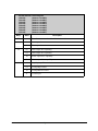
2.3.3 Spectrum Spreader
When enabled, the spectrum spreader stretches and compresses the main clock in a complex pattern that
spreads the energy of the clock harmonics over a wider range of frequencies. Note that the spectrum
spreader cannot operate at frequencies above 115 MHz as it uses up too much of the available clock
period, so care must be exercised when using the main PLL.
Figure 2.1 Effects of Spectrum Spreader
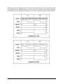
There are three settings that correspond to normal and strong spreading in the 0–50 MHz and >50 MHz
main clock range. Each setting will affect the clock cycle differently; the maximum cycle shortening (at
1.8 V and 25°C) is shown in Table 2-4 below.
Table 2-4. Spectrum Spreader Settings
0–50 MHz
50 - 150 MHz
GCM0R
Value
—
Normal
01xxxxxx
Normal spreading of frequencies
over 50 MHz
Normal
Strong
00xxxxxx
Normal spreading of frequencies
up to 50 MHz; strong spreading of
frequencies over 50 MHz
3 ns
Strong
—
10xxxxxx
Strong spreading of frequencies up
to 50 MHz; normal spreading of
frequencies over 50 MHz
4.5 ns
Rabbit 6000 User’s Manual
Description
digi.com
Max. Cycle
Shortening
2.3 ns
22
The spectrum spreader either stretches or shrinks the low plateau of the clock by a maximum of 3 ns for the
normal spreading and up to 4.5 ns for the strong spreading. If the clock doubler is used, this will cause an
additional asymmetry between alternate clock cycles.
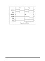
Harmonics (dB)
Both normal and strong modes reduce clock harmonics by approximately 15 dB for frequencies above 100
MHz; for lower frequencies the strong setting has a greater effect in reducing the peak spectral strength as
shown in Figure 2.2.
15
Strong Spreading
10
Normal Spreading
5
50
100
150
200
250
300
350
Frequency (MHz)
Figure 2.2 Peak Spectral Amplitude Reduction by Spectrum Spreader
Two registers control the clock spectrum spreader. These registers must be loaded in a specific manner
with proper time delays. GCM0R is only read by the spectrum spreader at the moment when the spectrum
spreader is enabled by setting bit 7 of GCM1R. If bit 7 of GCM1R is cleared (when disabling the spectrum
spreader), there is up to a 500-clock delay before the spectrum spreader is actually disabled. The proper
procedure is to clear GCM1R, wait for 500 clocks, set GCM0R, and then enable the spreader by writing a
1 to bit 7 of GCM1R.
The spectrum spreader is applied to the main clock before the clock doubler, so if both are enabled there
will be additional asymmetry between alternate clock cycles.If the clock doubler is used, the spectrum
spreader affects every other cycle and reduces the clock high time. If the doubler is not used, then the
spreader affects every clock cycle, and the clock low time is reduced.
Rabbit 6000 User’s Manual
digi.com
23
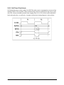
2.3.4 Clock Doubler
The clock doubler allows a lower frequency crystal to be used for the main oscillator and to provide an
added range over which the clock frequency can be adjusted. The clock doubler is controlled via the
Global Clock Double Register (GCDR).
The clock doubler uses an on-chip delay circuit that must be programmed by the user at startup if there is a
need to double the clock. Table 2-5 lists the recommended delays in GCDR for various oscillator or crystal
frequencies.
Table 2-5. Recommended Delays Set In GCDR for Clock Doubler
Recommended GCDR Value
Frequency Range
0x0F
7.3728 MHz
0x0B
7.3728–11.0592 MHz
0x09
11.0592–16.5888 MHz
0x06
16.5888–20.2752 MHz
0x03
20.2752–52.8384 MHz
0x01
52.8384–77.4144 MHz
0x00
>77.4144 MHz
Rabbit 6000 User’s Manual
digi.com
24
When the clock doubler is used and there is no subsequent division of the clock, the output clock will be
asymmetric, as shown in Figure 2.3.
Figure 2.3 Effect of Clock Doubler
The doubled-clock low time is subject to wide (50%) variation since it depends on process parameters,
temperature, and voltage. The times given above are for a core supply voltage of 1.8 V and a temperature
of 25°C. The values increase or decrease by 1% for each 5°C increase or decrease in temperature. The
doubled clock is created by xor’ing the delayed and inverted clock with itself. If the original clock does
not have a 50-50 duty cycle, then alternate clocks will have a slightly different length. Since the duty cycle
of the built-in oscillator can be as asymmetric as 52%/48%, the clock generated by the clock doubler will
exhibit up to a 4% variation in period on alternate clocks. The memory access time is not affected because
the memory bus cycle is 2 clocks long and includes both a long and a short clock, resulting in no net change
due to asymmetry. However, if an odd number of wait states is used, then the memory access time will be
affected slightly.
Rabbit 6000 User’s Manual
digi.com
25
The maximum allowed clock speed must be reduced slightly if the clock is supplied via the clock doubler.
The only signals clocked on the falling edge of the clock are the memory and I/O write pulses, and the
early option memory output enable. See Chapter 5 for more information on the early output enable and
write enable options.
The power consumption is proportional to the clock frequency, and for this reason power can be reduced
by slowing the clock when less computing activity is taking place. The clock doubler provides a convenient method of temporarily speeding up or slowing down the clock as part of a power management
scheme.
2.3.5 32 kHz Clock
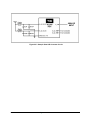
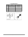
The 32.768 kHz clock is used to drive the asynchronous serial bootstrap, the real-time clock, the periodic
interrupt, and the watchdog timers; see Section 4.3 for detailed descriptions of these features. If these features are not used in a design, the use of the 32 kHz clock is optional.
A self-contained external oscillator is the recommended oscillator circuit for the Rabbit 6000, but a tunable
oscillator circuit such as the one shown below may be used. The values of resistors and capacitors may
need to be adjusted for various frequencies and crystal load capacitances. Rabbit’s Technical Note TN235,
External 32.768 kHz Oscillator Circuits, is available on the Rabbit Web site and goes into this circuit
in detail.
Figure 2.4 Basic 32.768 kHz Oscillator Circuit
Rabbit 6000 User’s Manual
digi.com
26
The 32.768 kHz circuit consumes microampere-level currents and has a very high impedance, making it
susceptible to noise, moisture, and environmental contaminants. It is strongly recommended to conformally coat this circuit to limit the effects of humidity and dust on the oscillation frequency. Details about
this requirement are available in Technical Note TN303, “Conformal Coating”, from the Rabbit Web site.
The need for a conformal coating can be avoided by using a single external clock chip.
The 32.768 kHz oscillator is slow to start oscillating after power-on. The startup delay may be as much as
5 seconds. For this reason, a wait loop in the BIOS waits until this oscillator is oscillating regularly before
continuing the startup procedure. If the clock is battery-backed, there will be no startup delay since the
oscillator is already oscillating. Crystals with low series resistance (R < 35 k) will start faster.
The 32 kHz oscillator can be used to drive the processor and the peripheral clock to provide significant
power savings in “ultra-sleepy” modes. The 32 kHz oscillator can be divided by 2, 4, 8, or 16 to provide
clock speeds as low as 2.048 kHz, although there are limitations on use of the 1MB internal RAM at those
low clock speeds (See Section 5.3.1, “Internal RAM”). Special self-timed chip selects are available to keep
the memory devices enabled for as short a time as possible when an ultra-sleepy mode is enabled; see
Chapter 36 for more details on reducing power consumption.
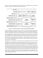
Table 2-6. Ultra-Sleepy Clock Modes
GPSCR
Setting
Processor and
Peripheral Clock
xxxxx000
32.768 kHz
xxxxx100
16.384 kHz
xxxxx101
8.192 kHz
xxxxx110
4.096 kHz
xxxxx111
2.048 kHz
When the 32 kHz clock is enabled as the CPU clock, the periodic interrupt is disabled automatically. The
real-time clock and watchdog timers keep running, and use the full 32 kHz clock speed even when the processor and peripheral clocks use a divider on the 32 kHz clock.
Rabbit 6000 User’s Manual
digi.com
27
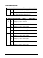
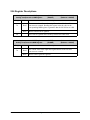
2.4 Register Descriptions
Global Control/Status Register
(GCSR)
(Address = 0x0000)
Bit(s)
Value
Description
7:5
000
No reset or watchdog timer timeout since the last read.
(rd-only)
010
The watchdog timer timed out. These bits will be cleared by reading the
register.
110
Hardware reset occurred. These bits will be cleared by reading the
register.
111
Power-on reset occurred. These bits will be cleared by reading the
register.
5
(write)
0
No effect on the Periodic interrupt.
1
Force a Periodic interrupt to be pending.
4:2
000
Processor clock from the main clock, divided by 8.
Peripheral clock from the main clock, divided by 8.
001
Processor clock from the main clock, divided by 8.
Peripheral clock from the main clock.
010
Processor clock from the main clock.
Peripheral clock from the main clock.
011
Processor clock from the main clock, divided by 2.
Peripheral clock from the main clock, divided by 2.
100
Processor clock from the 32 kHz clock, optionally divided via GPSCR.
Peripheral clock from the 32 kHz clock, optionally divided via GPSCR.
101
Processor clock from the 32 kHz clock, optionally divided via GPSCR.
Peripheral clock from the 32 kHz clock, optionally divided via GPSCR.
The main clock is disabled.
110
Processor clock from the main clock, divided by 4.
Peripheral clock from the main clock, divided by 4.
111
Processor clock from the main clock, divided by 6.
Peripheral clock from the main clock, divided by 6.
00
Periodic interrupts are disabled.
01
Periodic interrupts use Interrupt Priority 1.
10
Periodic interrupts use Interrupt Priority 2.
11
Periodic interrupts use Interrupt Priority 3.
1:0
Rabbit 6000 User’s Manual
digi.com
28
Global Clock Modulator 0 Register
(GCM0R)
(Address = 0x000A)
Bit(s)
Value
Description
7:6
00
Clock dither in 1 ns steps, from 0 ns to 26 ns. Do not modify while the
dither function is enabled.
01
Clock dither in 0.5 ns steps, from 0 ns to 13 ns.
10
Clock dither in 2 ns steps, from 0 ns to 52 ns.
11
This bit combination is reserved and must not be used.
5:4
These bits are reserved and should be written with zeros.
4:0
System PLL loop divider value. All zeros is not a valid value for the PLL
loop divider. The PLL output frequency is the input frequency divided by
the value of the PLL pre-divider, and multiplied by the value of the PLL
loop divider. Neither divider value should not be modified while the PLL
is supplying the clock to the system.
Global Clock Modulator 1 Register
(GCM1R)
(Address = 0x000B)
Bit(s)
Value
Description
7
0
Disable the clock dither function. The disable does not take effect until
the dither pattern has returned to the 0 ns base delay value.
1
Enable the clock dither function.
6:5
These bits are reserved and should be written with zeros.
3:0
System PLL pre-divider value. All zeros is not a valid value for the PLL
pre-divider. Neither divider value should not be modified while the PLL
is supplying the clock to the system.
Rabbit 6000 User’s Manual
digi.com
29
Global Clock Double Register
(GCDR)
(Address = 0x000F)
Bit(s)
Value
7
0
Disable system PLL.
1
Enable system PLL. Setting this bit does not select the system PLL as the clock
source.
6:5
4:0
Description
These bits are reserved and should always be written with zeros.
00000
The clock doubler circuit is disabled.
00001
9 nS nominal Low time.
00010
10.5 nS nominal Low time.
00011
12 nS nominal Low time.
00100
13.5 nS nominal Low time.
00101
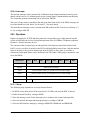
15 nS nominal Low time.
00110
16.5 nS nominal Low time.
00111
18 nS nominal Low time.
01000
19.5 nS nominal Low time.
01001
21 ns nominal Low time.
01010
22.5 ns nominal Low time.
01011
24 ns nominal Low time.
01100
25.5 ns nominal Low time.
01101
27 ns nominal Low time.
01110
28.5 ns nominal Low time.
01111
30 ns nominal Low time.
10001
4.5 nS nominal Low time.
10010
6 nS nominal Low time.
Rabbit 6000 User’s Manual
digi.com
30
Global Output Control Register
(GOCR)
(Address = 0x000E)
Bit(s)
Value
7:6
00
CLK pin is driven with peripheral clock.
01
CLK pin is driven with peripheral clock divided by 2.
10
CLK pin is low.
11
CLK pin is high.
00
STATUS pin is active (low) during a first opcode byte fetch.
01
STATUS pin is active (low) during an interrupt acknowledge.
10
STATUS pin is low.
11
STATUS pin is high.
00
/WDTOUT pin functions normally.
01
Enable /WDTOUT for test mode. Reserved for internal use only.
10
/WDTOUT pin is low (1 cycle min, 2 cycles max, of 32 kHz).
11
This bit combination is reserved and should not be used.
00
/BUFEN pin is active (low) during external I/O cycles.
01
/BUFEN pin is active (low) during data memory accesses.
10
/BUFEN pin is low.
11
/BUFEN pin is high.
5:4
3:2
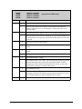
1:0
Rabbit 6000 User’s Manual
Description
digi.com
31
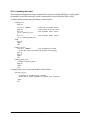
Master System Configuration Register
(MSCR)
(Address = 0x0434)
Bit(s)
Value
7
0
CPU clock direct from oscillator.
1
CPU clock from system PLL output (divided by two). Response to this
setting may be delayed until the PLL output is stable (roughly 200 µs
after enabling the system PLL, uses 32 kHz clock to generate delay).
6
5
Description
This bit is reserved and should be written as zero.
0
Clock on-chip 10/100 PHY from system oscillator.
1
Enable embedded oscillator in the internal 10-100 PHY. If using this
option, the oscillator must be enabled at least 500 ns before the PHY is
enabled in ENPR. This delay must be created in software.
0
No reset of the internal 10/100 PHY. Reads always return zero.
(Writeonly)
1
Reset the internal 10/100 PHY hardware. This command must not be
issued until at least 600 ms after the internal PHY has been enabled in
ENPR. This delay must be created in software.
3:2
00
FIMB clock is disabled.
01
FIMB clock is identical to the CPU clock.
10
This bit combination is reserved and should not be used.
11
FIMB clock from system PLL output. Response to this setting may be
delayed until the PLL output is stable (roughly 200 us after enabling the
system PLL, uses 32 kHz clock to generate delay).
00
FIMA clock is disabled.
01
FIMA clock is identical to the CPU clock.
10
This bit combination is reserved and should not be used.
11
FIMA clock from system PLL output. Response to this setting may be
delayed until the PLL output is stable (roughly 200 µs after enabling the
system PLL, uses 32 kHz clock to generate delay).
4
1:0
Rabbit 6000 User’s Manual
digi.com
32
Master System Status Register
Bit(s)
Value
7:6
5
(MSSR)
(Address = 0x0435)
Description
These bits are reserved and should be written with zeros.
0
Direct Wi-Fi clock input.
1
Enable Wi-Fi crystal oscillator.
0
Direct USB clock input.
1
Enable USB crystal oscillator.
3
0
Normal operation.
(Readonly)
1
Small package address and data bus option enabled (TEST = 0xF or 0xC).
2
0
Large package.
(Readonly)
1
Small package.
1
0
Wi-Fi PLL not enabled or output not stable.
(Readonly)
1
Wi-Fi PLL is enabled, with stable output.
0
0
System PLL not enabled or output not stable.
(Readonly)
1
System PLL is enabled, with stable output.
4
Rabbit 6000 User’s Manual
digi.com
33
Enable Network Port Register
(ENPR)
(Address = 0x0430)
Bit(s)
Value
7
0
Disable Network Port C (the Wi-Fi port).
1
Enable Network Port C (the Wi-Fi port).
0
Disable Network Port B (the 10/100Base-T Ethernet port).
1
Enable Network Port B (the 10/100Base-T Ethernet port).
0
Disable Network Port D (the USB port).
1
Enable Network Port D (the USB port).
0
Internal 10/100 PHY. This bit is ignored unless bit 6 of this register is also
set, at which point the internal PHY is powered up.
1
External 10/100 PHY.
00
Network Port D interrupts are disabled.
01
Network Port D interrupts use Interrupt Priority 1.
10
Network Port D interrupts use Interrupt Priority 2.
11
Network Port D interrupts use Interrupt Priority 3.
00
Network Port C interrupts are disabled.
01
Network Port C interrupts use Interrupt Priority 1.
10
Network Port C interrupts use Interrupt Priority 2.
11
Network Port C interrupts use Interrupt Priority 3.
6
5
4
3:2
1:0
Rabbit 6000 User’s Manual
Description
digi.com
34
3. RESET AND BOOTSTRAP
3.1 Overview
The Rabbit 6000’s /RESET pin initializes everything in the processor except for the real-time clock registers, the contents of the battery-backed onchip-encryption RAM and the 32K battery-backed SRAM. If a
write cycle is in progress, it waits until the write cycle is completed to avoid potential memory corruption.
After reset, the Rabbit 6000 checks the state of the SMODE and SYSCFG pins. Depending on the state of
the SMODE pins, it either begins normal operation by fetching instruction bytes from memory bank zero,
which is mapped to either /CS0 or /CS3 depending on the state of the SYSCFG pin, or it enters a special
bootstrap mode where it fetches bytes from either Serial Port A or the slave port. In this mode, bytes can
be written to internal registers to set up the Rabbit 6000 for a particular configuration, or to memory to
load a program. The processor can begin normal operation once the bootstrap operation is completed.
Rabbit 6000 User’s Manual
digi.com
35
3.1.1 Block Diagram
3.1.2 Registers
Register Name
Slave Port Control Register
Rabbit 6000 User’s Manual
Mnemonic
I/O Address
R/W
Reset
SPCR
0x0024
R/W
0xx00000
digi.com
36
3.2 Dependencies
3.2.1 I/O Pins
SMODE0, SMODE1 — When the Rabbit 6000 is first powered up or when it is reset, the state of the
SMODE0 and SMODE1 pins controls its operation.
SYSCFG — When the Rabbit 6000 is first powered up or when it is reset, the state of this pin controls
whether memory bank zero is mapped to /CS0 or the internal SRAM (/CS3).
/RESET — Pulling the /RESET pin low will initialize everything in the Rabbit 6000 except for the realtime clock registers, the 32K battery-backed RAM and the onchip-encryption RAM.
/CS1 — During reset the impedance of the /CS1 pin is high, and all other memory and I/O control signals
are held high. The special behavior of /CS1 allows an external RAM to be powered by the same source as
the VBATIO pin (which powers /CS1). In this case, a pullup resistor is required on /CS1 to keep the RAM
deselected during powerdown.
RESOUT — The RESOUT pin, which is powered by the backup battery, is high during reset and powerdown as long as VBAT and VBATIO are present, but low at all other times, and can be used to control an
external power switch to disconnect VDDIO from VBATIO when the main power source is removed.
3.2.2 Clocks
The processor requires a 32 kHz clock input to generate the 2400 bps internal clock required for asynchronous serial bootstrap, which is used when booting via Dynamic C and the Rabbit Field Utility. No 32 kHz
clock is required for either clocked serial or slave port bootstrap.
When the processor comes out of reset, the CPU clock and peripheral clocks are both in divide-by-8 mode.
3.2.3 Other Registers
Register
SPCR
Function
Enable/disable processor monitoring of SMODE
pins; read current state of SMODE pins.
3.2.4 Interrupts
There are no interrupts associated with reset or bootstrap.
Rabbit 6000 User’s Manual
digi.com
37
3.3 Operation
Pulling the /RESET pin low will initialize everything in the Rabbit 6000 except for the real-time clock registers, the 32K battery-backed RAM and the onchip-encryption RAM. The reset of the Rabbit 6000 is
delayed until any write cycles in progress are completed; the reset takes effect as soon as no write cycles
are occurring. The reset sequence requires a minimum of 128 cycles of the main clock to complete in
either case.
During reset, the impedance of the /CS1 pin is high and all other memory and I/O control signals are held
high. The special behavior of /CS1 allows an external RAM to be powered by the same source as the
VBATIO pin (which powers /CS1). In this case, a pullup resistor is required on /CS1 to keep the RAM
deselected during powerdown. The RESOUT pin, which is powered by the backup battery, is high during
reset and powerdown as long as VBAT and VBATIO are present, but low at all other times, and can be
used to control an external power switch to disconnect VDDIO from VBATIO when the main power
source is removed.
Table 3-1 lists the condition of the processor after reset takes place. The state of all registers after reset is
provided in the chapter describing the specific peripheral.
Table 3-1. Rabbit 6000 Condition After Reset
Function
Operation After Reset
CPU Clock,
Peripheral Clock
Divide-by-8 mode
Clock Doubler,
Clock Dither
Disabled
Memory Bank 0
Control Register
/CS0, /OE0, write-protected,
4 wait states
Memory Advanced
Control Register
8-bit interface
CPU Registers:
PC, SP, IIR, EIR,
HTR
0x0000
Interrupt Priority
(IP Register)
0xFF (Priority 3)
Watchdog Timer
Enabled (2 seconds)
Secondary
Watchdog Timer
Disabled
Rabbit 6000 User’s Manual
digi.com
38
The processor checks the SMODE and SYSCFG pins after the /RESET signal is inactive. Table 3-2 summarizes what happens.
Table 3-2. SMODE Pin Settings
SMODE Pins [1,0]
SYSCFG
Operation
00
0
No bootstrap; code is fetched from address 0x0000
on /CS0, /OE0.The internal SRAM is enabled as a
16-bit memory device.
00
1
No bootstrap; code is fetched from address 0x0000
on /CS3, /OE0. The internal SRAM is enabled as a
16-bit memory device.
01
x
Bootstrap from the slave port.
10
x
Bootstrap from Serial Port A, serial flash mode.
11
x
Bootstrap from Serial Port A, asynchronous mode.
If both SMODE pins are zero, the Rabbit 6000 begins fetching instructions from the memory device
mapped into memory bank 0. When SYSCFG is low, memory bank 0 is set to /CS0 and /OE0. If SYSCFG
is high, memory bank 0 is set to /CS3 and /OE0. In both cases, the internal SRAM is selected in 16-bit
mode. If a 16-bit memory is used in memory bank 0, the first section of code must immediately select the
16-bit bus mode. Chapter 5 provides a short sample program to do this.
If either of the SMODE pins is high, the processor will enter the bootstrap mode and accept triplets from
Serial Port A, the serial flash bootstrap port, or the slave port, depending on the SMODE pin selection. It is
good practice to place pulldown resistors on the SMODE pins to ensure the proper operation of your
design.
In the bootstrap mode, the processor inhibits the normal memory fetch, and instead fetches instructions
from a small internal boot ROM. This program reads triplets of three bytes from the selected peripheral.
The first byte is the most-significant byte of a 16-bit address, the second byte is the least-significant byte
of the address, and the third byte is the data to be written. If the uppermost bit of the address is 1, then the
address is assumed to be an internal register address instead of a memory address, and the data are written
to the appropriate register instead. For example, a triplet of (0x04, 0x34, 0x5A) will write 0x5A to logical
memory address 0x0434, while a triplet of (0x80, 0x34, 0x5A) will write 0x5A to processor register 0x34.
Processor registers with addresses above 0xFF are not accessible in the bootstrap mode.
The boot ROM program waits for data to be available; each byte received automatically resets the watchdog timer with a 2-second timeout. Bytes must be received quickly enough to prevent timeout (or the
watchdog must be disabled).
The device checks the state of the SMODE pins each time it jumps back to the start of the ROM program
and responds according to the current state. In addition, by setting bit 7 of the Slave Port Control Register
(SPCR) high, the processor can be told to ignore the state of the SMODE pins and continue normal operation.
Rabbit 6000 User’s Manual
digi.com
39
Note that the processor can be told to re-enter bootstrap mode at any time by setting bit 7 of SPCR low;
once this occurs and the least significant four bits of the current PC address are zero, the processor will
sample the state of the SMODE pins and respond accordingly. This feature allows in-line downloading
from the selected bootstrap port; once the download is complete, bit 7 of SPCR can be set high and the
processor will continue operating from where it left off.
As a security feature, any attempt to enter the bootstrap mode from either the SMODE pins or by writing
to bit 7 of the SPCR will erase the data stored in the onchip-encryption RAM. This prevents loading a
small program in memory to read out the data.
3.3.1 Asynchronous Serial Bootstrap
When the asynchronous serial bootstrap mode is selected by the SMODE pins, the Rabbit 6000 will begin
accepting triplets at 2400 bps on Serial Port A. The baud rate is generated from the 32 kHz clock input, so
a 32 kHz clock is required for this mode.
3.3.2 Serial Flash Bootstrap
When the serial flash bootstrap mode is selected by the SMODE pins, the Rabbit 6000 will enable the SPI
serial flash bootstrap port on pins PD4, PD5, PD6, and PB0; the pins’ functionality is listed in Table 3-3
below. Note that these pins can be used for Serial Port B in normal operation, so the serial flash may be
accessed with that serial port during normal operation.
Table 3-3. Serial Flash Bootstrap Pin Functions
Pin
SPI Signal
Operation
PD4
MOSI
Rabbit data transmit (to serial flash)
PD5
MISO
Rabbit data receive (from serial flash)
PD6
CS
PB0
SCK
Chip select (to serial flash)
Serial clock (output to serial flash)
The Rabbit 6000 divides the main clock by 64 to provide the SPI clock for the serial flash bootstrap. Once
this mode is entered, the Rabbit 6000 will send the byte sequence “0x03 0x00 0x00 0x00”, which is an
industry-standard command that enables continuous read mode starting at serial flash address 0x0.
Figure 3.1 provides a sample timing diagram. The Rabbit 6000 will then read triplets out of the serial flash
until the bootstrap mode is exited.
Figure 3.1 SPI Timing Diagram for Serial Flash Bootstrap Mode
Rabbit 6000 User’s Manual
digi.com
40
3.3.3 Parallel Bootstrap
When the parallel bootstrap mode is selected by the SMODE pins, the Rabbit 6000 will enable the parallel
slave port interface on Parallel Ports A and B, and will wait for triplets to be sent to that interface. See
Chapter 21 for more details on the operation of the slave port.
3.4 Register Descriptions
Slave Port Control Register
(SPCR)
Bit(s)
Value
7
0
Program fetch as a function of the SMODE pins.
1
Ignore the SMODE pins program fetch function.
6:5
4:2
1:0
(Address = 0x0024)
Description
Read
These bits report the state of the SMODE pins.
Write
These bits are ignored and should be written with zero.
000
Disable the slave port. Parallel Port A is a byte-wide input port.
001
Disable the slave port. Parallel Port A is a byte-wide output port.
010
Enable the slave port, with /SCS from Parallel Port E bit 7.
011
Enable the external I/O bus. Parallel Port A is used for the data bus and
Parallel Port B[7:2] is used for the address bus.
100
This bit combination is reserved and should not be used.
101
This bit combination is reserved and should not be used.
110
Enable the slave port, with /SCS from Parallel Port B bit 6.
111
Enable the external I/O bus. Parallel Port A is used for the data bus and
Parallel Port B[7:0] is used for the address bus.
00
Slave port interrupts are disabled.
01
Slave port interrupts use Interrupt Priority 1.
10
Slave port interrupts use Interrupt Priority 2.
11
Slave port interrupts use Interrupt Priority 3.
Rabbit 6000 User’s Manual
digi.com
41
4. SYSTEM MANAGEMENT
4.1 Overview
There are a number of basic system peripherals in the Rabbit 6000 processor, some of which are covered in
later chapters. The peripherals covered in this chapter are the periodic interrupt, the real-time clock, the
watchdog timers, the battery-backed onchip-encryption RAM, and some of the miscellaneous output pins
and their control and processor registers that provide the processor ID and revision numbers.
The periodic interrupt, when enabled, is generated every 16 clocks of the 32 kHz clock (every 488 µs, or
2.048 kHz). This interrupt can be used to perform periodic tasks.
The real-time clock (RTC) consists of a 48-bit counter that is clocked by the 32 kHz clock. It is powered
by the VBAT pin, and so can be battery-backed. The value in the counter is not affected by reset, and can
only be set to zero by writing to the RTC control register. The 48-bit width provides a 272-year span before
rollover occurs.
There are two watchdog timers in the Rabbit 6000, both clocked by the 32 kHz clock. The main watchdog
timer can be set to time out from 250 ms to 2 seconds, and resets the processor if not reloaded within that
time. Its purpose is to restart the processor when it detects that a program gets stuck or disabled.
The secondary watchdog timer can time out from 30.5 µs up to 7.8 ms, and generates a Priority 3 secondary watchdog interrupt when it is not reset within that time. The primary use for the secondary watchdog is
to act as a safety net for the periodic interrupt — if the secondary watchdog is reloaded in the periodic
interrupt, it will count down to zero if the periodic interrupt stops occurring. In addition, it can be used as a
periodic interrupt on its own.
The battery-backed onchip-encryption RAM consists of 32 bytes of memory that are powered by the
VBAT pin (note that this RAM is separate from the battery-backed 32 KB SRAM). Their values are not
affected by a reset, but are erased if the state of the SMODE pins changes. These 32 bytes are intended for
storing sensitive data (such as an encryption key) somewhere other than an external memory device. The
“tamper-protection” erase feature erases these bytes if an attempt is made to load a program into the
onchip RAM to read out the bytes.
A feature new to the Rabbit 6000 is a 14-bit CPU clock cycle counter. This counter counts the number of
CPU cycles that occur during one 32 kHz clock period. This is useful for determining the frequency of the
main CPU oscillator which can be used in baud rate calculations as well as other CPU clock dependant
features.
The following other registers are also described in this chapter.
• Global Output Control Register (GOCR), which controls the behavior of the CLK, STATUS, /WDT,
and /BUFEN pins
• Global CPU Register (GCPU), which holds the identification number of the processor.
• Global Revision Register (GREV), which hold the revision number of the processor.
Rabbit 6000 User’s Manual
digi.com
42
4.1.1 Block Diagram
Rabbit 6000 User’s Manual
digi.com
43
4.1.2 Registers
Register Name
Mnemonic
I/O Address
R/W
Reset
Global Control/Status Register
GCSR
0x0000
R/W
11000000
Real-Time Clock Control Register
RTCCR
0x0001
W
00000000
Real-Time Clock Byte 0 Register
RTC0R
0x0002
R/W
xxxxxxxx
Real-Time Clock Byte 1 Register
RTC1R
0x0003
R
xxxxxxxx
Real-Time Clock Byte 2 Register
RTC2R
0x0004
R
xxxxxxxx
Real-Time Clock Byte 3 Register
RTC3R
0x0005
R
xxxxxxxx
Real-Time Clock Byte 4 Register
RTC4R
0x0006
R
xxxxxxxx
Real-Time Clock Byte 5 Register
RTC5R
0x0007
R
xxxxxxxx
Watchdog Timer Control Register
WDTCR
0x0008
W
00000000
Watchdog Timer Test Register
WDTTR
0x0009
W
00000000
Secondary Watchdog Timer Register
SWDTR
0x000C
W
11111111
Global Output Control Register
GOCR
0x000E
R/W
00000000
Global ROM Configuration Register
GROM
0x002C
R
0xx00000
Global RAM Configuration Register
GRAM
0x002D
R
0xx00000
Global CPU Configuration Register
GCPU
0x002E
R
0xx00010
Global Revision Register
GREV
0x002F
R
0xx00000
VRAM00–
VRAM1F
0x0600–
0x061F
R/W
xxxxxxxx
Master System Configuration Register
MSCR
0x0434
R/W
00000000
Master System Status Register
MSSR
0x0435
R/W
00000x00
Battery-Backed Onchip-Encryption RAM
Bytes 00–1F
Rabbit 6000 User’s Manual
digi.com
44
4.2 Dependencies
4.2.1 I/O Pins
The CLK, STATUS, /WDTOUT, and /BUFEN pins are controlled by GOCR. Each of these pins can be
used as general-purpose outputs by driving them high or low.
• The CLK pin can output the peripheral clock, the peripheral clock divided by two, or be driven high or
low.
• The STATUS pin can be active low during the first byte of each opcode fetch, active low during an
interrupt acknowledge, or driven high or low.
• The /WDTOUT pin can be active low whenever the watchdog timer resets the device or driven low.
• The /BUFEN pin can be active low during external I/O cycles, active low during data memory cycles,
or driven high or low.
The values in the battery-backed onchip-encryption RAM bytes are cleared if the signal on the SMODE
pins changes state.
4.2.2 Clocks
The periodic interrupt, real-time clock, watchdog timer, and secondary watchdog timer require the 32 kHz
clock.
4.2.3 Interrupts
The periodic interrupt is enabled in GCSR, and will occur every 488 µs. It is cleared by reading GCSR. It
can operate at Priority 1, 2, or 3.
The secondary watchdog interrupt will occur whenever the secondary watchdog is enabled and allowed to
count down to zero. It is cleared by restarting the secondary watchdog by writing 0x5F to WDTCR or writing a new timeout value to SWDTR. The secondary watchdog interrupt always occurs at Priority 3.
Rabbit 6000 User’s Manual
digi.com
45
4.3 Operation
4.3.1 Periodic Interrupt
The following steps explain how a periodic interrupt is used.
1. Write the vector to the interrupt service routine to the internal interrupt table.
2. Enable the periodic interrupt by writing to GCSR.
3. The interrupt request is cleared by reading from GCSR.
A sample interrupt handler is shown below.
periodic_isr::
push af
ioi ld a, (GCSR)
; clear the interrupt request and get status
; handle any periodic tasks here
pop af
ipres
ret
4.3.2 Real-Time Clock
The real-time clock consists of six 8-bit registers that together comprise a 48-bit value. The real-time clock
is not synchronized to the read operation, so the least-significant byte should be read twice and checked for
matching values; if the two reads do not match, then the real-time clock may have been updating during
the read and should be read again.
Writing to RTC0R latches the current real-time clock value into the RTCxR holding registers, so the following sequence should be used to read the real-time clock.
1. Write any value to RTC0R and then read back a value from RTC0R.
2. Write a value to RTC0R again, and again read back a value from RTC0R.
3. If the two values do not match, repeat Step 2 until the last two readings are identical.
4. At this point, registers RTC1R through RTC6R can also be read and used.
Note that the periodic interrupt and the real-time clock are clocked by the same edge of the 32 kHz clock;
if read from the periodic interrupt, the count is guaranteed to be stable and only needs to be read once
(assuming it occurs within one clock of the 32 kHz clock).
The real-time clock can be reset by writing the sequence 0x40 – 0x80 to RTCCR. It can be reset and left in
the byte increment mode by writing 0x40 – 0xC0 to RTCCR and then writing bytes repeatedly to RTCCR
to increment the appropriate bytes of the real-time clock. The byte increment mode is disabled by writing
0x00 to RTCCR.
Rabbit 6000 User’s Manual
digi.com
46
4.3.3 Watchdog Timer
The watchdog timer is enabled on reset with a 2-second timeout. Unless specific data are written to
WDTCR before that time expires, the processor will be reset. The watchdog timer can be disabled by writing a sequence of two bytes to WDTTR as described in the register description.
Table 4-1. Watchdog Timer Settings
WDTCR Value
Effect
0x5A
Restart watchdog timer with 2-second timeout.
0x57
Restart watchdog timer with 1-second timeout.
0x59
Restart watchdog timer with 500-millisecond timeout.
0x53
Restart watchdog timer with 250-millisecond timeout.
0x5F
Restart the secondary watchdog timer.
The watchdog timer also contains a special test mode that speeds up the timeout period by clocking it with
the peripheral clock instead of the 32 kHz clock. This mode can be enabled by writing to WDTTR.
4.3.4 Secondary Watchdog Timer
The secondary watchdog timer is disabled on reset. The following steps explain how to use the secondary
watchdog timer.
1. Write the vector to the interrupt service routine to the internal interrupt table.
2. Write the desired timeout period to SWDTR. This also enables the secondary watchdog timer.
3. Restart the secondary watchdog timer by either writing the timeout period to SWDTR or writing
0x5F to WDTCR.
If the secondary watchdog timer counts down to zero, a Priority 3 secondary watchdog interrupt will occur.
This interrupt request is cleared by writing a new timeout value to SWDTR. A sample interrupt handler is
shown below.
secwd_isr::
push af
; determine why the interrupt occurred and take appropriate
action
ld a, 0x40
ioi ld (SWDTR), a
; timeout period of 0x40/32kHz = 1.95ms
; clear the interrupt request
pop af
ipres
ret
4.3.5 CPU Clock Cycle Counter
This counter counts the number of CPU cycles that occur during one 32 kHz clock period. The least significant 8 bits of this 14-bit counter are accessed by reading WDTCR, and the upper 6 bits are accessed by
reading WDTTR. This value is updated continually, so be careful to not change the main clock frequency
between reading the two registers.
Rabbit 6000 User’s Manual
digi.com
47
4.4 Register Descriptions
Global Control/Status Register
(GCSR)
(Address = 0x0000)
Bit(s)
Value
Description
7:5
000
No reset or watchdog timer timeout since the last read.
(rd-only)
010
The watchdog timer timed out. These bits will be cleared by reading the
register.
110
Hardware reset occurred. These bits will be cleared by reading the
register.
111
Power-on reset occurred. These bits will be cleared by reading the
register.
5
(write)
0
No effect on the Periodic interrupt.
1
Force a Periodic interrupt to be pending.
4:2
000
Processor clock from the main clock, divided by 8.
Peripheral clock from the main clock, divided by 8.
001
Processor clock from the main clock, divided by 8.
Peripheral clock from the main clock.
010
Processor clock from the main clock.
Peripheral clock from the main clock.
011
Processor clock from the main clock, divided by 2.
Peripheral clock from the main clock, divided by 2.
100
Processor clock from the 32 kHz clock, optionally divided via GPSCR.
Peripheral clock from the 32 kHz clock, optionally divided via GPSCR.
101
Processor clock from the 32 kHz clock, optionally divided via GPSCR.
Peripheral clock from the 32 kHz clock, optionally divided via GPSCR.
The main clock is disabled.
110
Processor clock from the main clock, divided by 4.
Peripheral clock from the main clock, divided by 4.
111
Processor clock from the main clock, divided by 6.
Peripheral clock from the main clock, divided by 6.
00
Periodic interrupts are disabled.
01
Periodic interrupts use Interrupt Priority 1.
10
Periodic interrupts use Interrupt Priority 2.
11
Periodic interrupts use Interrupt Priority 3.
1:0
Rabbit 6000 User’s Manual
digi.com
48
Real-Time Clock Control Register
(RTCCR)
(Address = 0x0001)
Bit(s)
Value
Description
7:0
0x00
No effect on the real-time clock counter, or disable the byte increment
function, or cancel the real-time clock reset command.
0x40
Arm the real-time clock for reset or byte increment. This command must
be written prior to either the real-time clock reset command or the first
byte increment write.
0x80
Reset all six bytes of the real-time clock counter to 0x00. The reset must
be preceded by writing 0x40 to arm the reset function.
0xC0
Reset all six bytes of the real-time clock counter to 0x00, and remain in
byte-increment mode in preparation for setting the time.
7:6
01
This bit combination must be used with every byte-increment write.
5:0
0
No effect on the real-time clock counter.
1
Increment the corresponding byte of the real-time clock counter.
Real-Time Clock x Register
(RTC0R)
(Address = 0x0002)
(RTC1R)
(Address = 0x0003)
(RTC2R)
(Address = 0x0004)
(RTC3R)
(Address = 0x0005)
(RTC4R)
(Address = 0x0006)
(RTC5R)
(Address = 0x0007)
Bit(s)
Value
7:0
Read
The current value of the 48-bit real-time clock counter is returned.
Write
Writing to RTC0R transfers the current count of the real-time clock to a
holding register while the real-time clock continues counting.
Rabbit 6000 User’s Manual
Description
digi.com
49
Watchdog Timer Control Register
(WDTCR)
(Address = 0x0008)
Bit(s)
Value
Description
7:0
0x5A
Restart the watchdog timer with a 2-second timeout period.
0x57
Restart the watchdog timer with a 1-second timeout period.
0x59
Restart the watchdog timer with a 500 ms timeout period.
0x53
Restart the watchdog timer with a 250 ms timeout period.
0x5F
Restart the secondary watchdog timer.
other
No effect on watchdog timer or secondary watchdog timer.
read
Return the least-significant 8bits of the CPU clock cycle counter.
Watchdog Timer Test Register
(WDTTR)
(Address = 0x0009)
Bit(s)
Value
Description
7:0
0x51
Clock the least significant byte of the watchdog timer from the peripheral
clock.
0x52
Clock the most significant byte of the watchdog timer from the peripheral
clock.
0x53
Clock both bytes of the watchdog timer, in parallel, from the peripheral
clock.
0x54
Disable the watchdog timer. This value, by itself, does not disable the
watchdog timer. Only a sequence of two writes, where the first write is
0x51, 0x52, or 0x53, followed by a write of 0x54, actually disables the
watchdog timer. The watchdog timer will be re-enabled by any other
write to this register.
other
Normal clocking (32 kHz clock) for the watchdog timer.
read
Return the most-significant 6 bits of the CPU clock cycle counter.
5:0
Rabbit 6000 User’s Manual
digi.com
50
Secondary Watchdog Timer Register
Bit(s)
Value
(SWDTR)
(Address = 0x000C)
Description
The time constant for the secondary watchdog timer is stored. This time
constant will take effect the next time that the secondary watchdog
counter counts down to zero. The timer counts modulo n + 1, where n is
the programmed time constant. The secondary watchdog timer can be
disabled by writing the sequence 0x5A – 0x52 – 0x44 to this register.
7:0
Global ROM Configuration Register
(GROM)
Bit(s)
Value
7
0
Program fetch as a function of the SMODE pins.
(Readonly)
1
Ignore the SMODE pins program fetch function.
6:5
Read
These bits report the state of the SMODE pins.
4:0
00000
ROM identifier for this version of the chip.
Description
Global RAM Configuration Register
(GRAM)
Bit(s)
Value
7
0
Program fetch as a function of the SMODE pins.
(Readonly)
1
Ignore the SMODE pins program fetch function.
6:5
Read
These bits report the state of the SMODE pins.
4:0
00010
RAM identifier for this version of the chip.
Rabbit 6000 User’s Manual
(Address = 0x002C)
(Address = 0x002D)
Description
digi.com
51
Global Output Control Register
(GOCR)
(Address = 0x000E)
Bit(s)
Value
7:6
00
CLK pin is driven with peripheral clock.
01
CLK pin is driven with peripheral clock divided by 2.
10
CLK pin is low.
11
CLK pin is high.
00
STATUS pin is active (low) during a first opcode byte fetch.
01
STATUS pin is active (low) during an interrupt acknowledge.
10
STATUS pin is low.
11
STATUS pin is high.
00
/WDTOUT pin functions normally.
01
Enable /WDTOUT for test mode. Reserved for internal use only.
10
/WDTOUT pin is low (1 cycle min, 2 cycles max, of 32 kHz).
11
This bit combination is reserved and should not be used.
00
/BUFEN pin is active (low) during external I/O cycles.
01
/BUFEN pin is active (low) during data memory accesses.
10
/BUFEN pin is low.
11
/BUFEN pin is high.
5:4
3:2
1:0
Description
Global CPU Register
(GCPU)
Bit(s)
Value
7
0
Program fetch as a function of the SMODE pins.
(Readonly)
1
Ignore the SMODE pins program fetch function.
6:5
Read
These bits report the state of the SMODE pins.
4:0
00100
CPU identifier for this version of the chip.
Rabbit 6000 User’s Manual
(Address = 0x002E)
Description
digi.com
52
Global Revision Register
(GREV)
Bit(s)
Value
7
0
Program fetch as a function of the SMODE pins.
(Readonly)
1
Ignore the SMODE pins program fetch function.
6:5
Read
These bits report the state of the SMODE pins.
4:0
00000
CPU identifier for this version of the chip.
(Address = 0x002F)
Description
Battery-Backed Onchip-Encryption RAM
(VRAM00)
(Address = 0x0600)
through
through
(VRAM31)
(Address = 0x061F)
Bit(s)
Value
7:0
Rabbit 6000 User’s Manual
Description
General-purpose RAM locations. Cleared by Intrusion Detect conditions.
digi.com
53
5. MEMORY MANAGEMENT
5.1 Overview
The Rabbit 6000 supports both 8-bit and 16-bit external flash and SRAM devices; three chip selects, and
two read/write-enable strobes allow up to six external devices to be attached at once. The 8-bit mode
allows 0, 1, 2, or 4 wait states to be specified for each device, and the 16-bit mode allows 0 to 7 wait states
depending on the settings. Both 8-bit and 16-bit page-mode devices are also supported.
In addition, the Rabbit 6000 contains 1 MB of internal high-speed RAM and 32 KB of battery-backed
SRAM (also high speed) that reside on their own chip select signal. They can both be enabled in either the
8-bit or the 16-bit mode.
The Rabbit 6000’s physical memory space contains four consecutive banks, each of which can be set for
equal sizes ranging from 128 KB up to 4 MB, providing a total physical memory range from 512 KB up to
16 MB. Each bank can be mapped to an individual chip-select/enable strobe pair for a memory device. In
addition, each bank can be divided into two equal-sized low and high sub banks with separate chip-select/
enable strobe mapping. Figure 5.1 shows a sample configuration.
Rabbit 6000 User’s Manual
digi.com
54
Figure 5.1 Mapping Rabbit 6000 Physical Memory Space
Either one or both of the two most significant address bits (which are used to select the quadrant) can be
inverted, providing the ability to bank-switch other pages from a larger memory device into the same
memory bank.
Code is executed in the 64 KB logical memory space, which is divided into four segments: root, data,
stack, and XMEM. The root segment is mapped directly to physical address 0x000000, while the data and
stack segments can be mapped to 4 KB boundaries anywhere in the physical space. The boundaries
between the root and data segments and the data and stack segments can be adjusted in 4 KB blocks as
well.
The XMEM segment is a fixed 8 KB, and points to a physical memory address block specified in the
LXPC register. It is possible to run code in the XMEM window, providing an easy means of storing and
executing code beyond the 64 KB logical memory space. Special call and return instructions to physical
addresses are provided that automatically update the LXPC register as necessary.
Rabbit 6000 User’s Manual
digi.com
55
Figure 5.2 Logical and Physical Memory Mapping
The Rabbit 2000 and 3000 had numerous instructions for reading and writing data to logical addresses, but
only had limited support for reading and writing data to a physical memory address. In the Rabbit 4000, a
wide range of instructions was provided to read and write to physical addresses. The same instructions can
be used to write to logical addresses. All of these instructions are available in the Rabbit 6000, as well as
new instructions for more operations using physical addresses.
The 64 KB logical memory space limitation can also be expanded by using the separate instruction and
data space mode. When this mode is enabled, address bit A16 is inverted for all data accesses in the root
and/or data segments, and the most-significant bit of the bank select bits is inverted for all data accesses in
the root and/or data segments before bank selection (physical device) occurs. These two features allow
both code and data to access separate 64 KB logical spaces instead of sharing a single space.
It is possible to protect memory in the Rabbit 6000 at three different levels—each of the memory banks
can be made read-only, physical memory can be write-protected in 64 KB blocks, and two of those 64 KB
blocks can be protected with a granularity of 4 KB. A Priority 3 interrupt will occur if a write is attempted
in one of the protected 64 KB or 4 KB blocks. In addition, it is possible to place limits around the code execution stack and generate an interrupt if a stack-related write occurs within 16 bytes of those limits.
The drive strength and slew rate can be controlled for the address bus, data bus, and memory strobes (other
than /CS1, which has fixed functionality). In addition, a 75 k pullup or pulldown resistor can be enabled
on the data bus.
Rabbit 6000 User’s Manual
digi.com
56
5.1.1 Block Diagram
Rabbit 6000 User’s Manual
digi.com
57
5.1.2 Registers
Register Name
Mnemonic
I/O Address
R/W
Reset
MMIDR
0x0010
R/W
00000000
STACKSEG
0x0011
R/W
00000000
Stack Segment LSB Register
STACKSEGL
0x001A
R/W
00000000
Stack Segment MSB Register
STACKSEGH
0x001B
R/W
00000000
DATSEG
0x0012
R/W
00000000
Data Segment LSB Register
DATSEGL
0x001E
R/W
00000000
Data Segment MSB Register
DATSEGH
0x001F
R/W
00000000
Segment Size Register
SEGSIZE
0x0013
R/W
11111111
Memory Bank 0 Control Register
MB0CR
0x0014
R/W
00001000
Memory Bank 1 Control Register
MB1CR
0x0015
R/W
xxxxxxxx
Memory Bank 2 Control Register
MB2CR
0x0016
R/W
xxxxxxxx
Memory Bank 3 Control Register
MB3CR
0x0017
R/W
xxxxxxxx
MMU Expanded Code Register
MECR
0x0018
R/W
00000000
Memory Timing Control Register
MTCR
0x0019
R/W
00000000
Memory Alternate Control Register
MACR
0x001D
R/W
00000000
Memory Bank 0 Low Control Register
MB0LCR
0x0400
R/W
00001000
Memory Bank 0 High Control Register
MB0HCR
0x0401
R/W
00001000
Memory Bank 1 Low Control Register
MB1LCR
0x0402
R/W
00001000
Memory Bank 1 High Control Register
MB1HCR
0x0403
R/W
00001000
Memory Bank 2 Low Control Register
MB2LCR
0x0404
R/W
00001000
Memory Bank 2 High Control Register
MB2HCR
0x0405
R/W
00001000
Memory Bank 3 Low Control Register
MB3LCR
0x0406
R/W
00001000
Memory Bank 3 High Control Register
MB3HCR
0x0407
R/W
00001000
Advanced /CS0 Control Register
ACS0CR
0x0410
R/W
00000000
Advanced /CS1 Control Register
ACS1CR
0x0411
R/W
00000000
Advanced /CS2 Control Register
ACS2CR
0x0412
R/W
00000000
RAM Segment Register
RAMSR
0x0448
R/W
00000000
WPnR
0x460 + n
W
00000000
MMU Instruction/Data Register
Stack Segment Register
Data Segment Register
Write-Protect n Register (n = 0–31)
Rabbit 6000 User’s Manual
digi.com
58
Register Name
Mnemonic
I/O Address
R/W
Reset
WPSAR
0x0480
W
00000000
Write-Protect Segment A Low Register
WPSALR
0x0481
W
00000000
Write-Protect Segment A High Register
WPSAHR
0x0482
W
00000000
Write-Protect Segment B Register
WPSBR
0x0484
W
00000000
Write-Protect Segment B Low Register
WPSBLR
0x0485
W
00000000
Write-Protect Segment B High Register
WPSBHR
0x0486
W
00000000
Stack Limit Control Register
STKCR
0x0444
R/W
00000000
Stack Low Limit Register
STKLLR
0x0445
W
xxxxxxxx
Stack High Limit Register
STKHLR
0x0446
W
xxxxxxxx
Address Bus Pin Control Register
ADPCR
0x04A0
W
xxx00000
Data Bus Pin Control Register
DBPCR
0x04A1
W
xxx00000
CPCR
0x04A2
W
xxx00000
Write-Protect Segment A Register
Control Pin Control Register
Rabbit 6000 User’s Manual
digi.com
59
5.2 Dependencies
5.2.1 I/O Pins
There are three chip select pins, /CS0, /CS1, and /CS2; two read strobes, /OE0 and /OE1; and two write
strobes, /WE0 and /WE1. /CS3 is available to the internal SRAMs only and does not come out to a pin.
There are 16 dedicated data bus pins, D0 through D15, and 25 dedicated address pins, A0 through A23,
and /A0 to allow byte access to 16 bit devices.
If the SYSCFG pin is held high on startup, the Memory Bank 0 Control Register and Memory Bank 0 Low
Control Register are set to a particular value that maps to the internal SRAM. See Section 5.3.1 for more
details.
The drive strength and slew rate are selectable for the address and data bus pins and for the memory strobe
pins (except /CS1) via ADPCR, DBPCR, and CPCR. /CS1 has a fixed setting of 8 mA drive and fast slew.
Internal pullup and/or pulldown resistors are also selectable on the data bus.
5.2.2 Clocks
All memory operations are clocked by the processor clock.
5.2.3 Interrupts
When a write is attempted to a write-protected 64 KB or 4 KB block, a write-protection violation interrupt
is generated. The interrupt request is cleared when it is handled. The write-protection violation interrupt
vector is in the IIR at offset 0x090. It is always set to Priority 3.
When a stack-related write is attempted to a region outside that set by the stack limit registers, a stack limit
violation occurs. The interrupt request is cleared when it is handled. The stack limit violation interrupt vector is in the IIR at offset 0x1B0. It is always set to Priority 3.
Rabbit 6000 User’s Manual
digi.com
60
5.3 Operation
5.3.1 Internal RAM
There are two internal RAM devices in the Rabbit 6000. A 1 MB RAM is located on /CS3, /OE0, /WE0,
and a 32 KB battery-backed SRAM is located on /CS3, /OE1, /WE1. Both of them can be run at speeds up
to 200 MHz with no additional wait states.
The 1 MB RAM is a pipelined device, meaning that the DMA peripheral can access it between code
fetches and data read/writes, providing a significant performance improvement for applications that use
DMA such as networking. However, there are some restrictions in the use of the 1 MB RAM:
1. If the 32 kHz clock is not present, its performance will be halved. This will not be noticeable unless
DMA is also operational.
2. The data contents will only be preserved if the main clock is greater than 12 MHz.
The internal 32 KB SRAM is powered by the VBAT pin. Its contents will be preserved as long as 1.2 V is
kept on VBAT.
5.3.2 Memory Management Unit (MMU)
Code execution takes place in the 64 KB logical memory space, which is divided into four segments: root,
data, stack, and extended (XMEM). The root segment is always mapped starting at physical address
0x000000, but the other segments can be remapped to start at any physical 4 KB block boundary.
The data and stack segment mappings are set by writing to the appropriate register, as shown in Table 5-1.
The DATASEG and STACKSEG registers provide backwards compatibility to the Rabbit 2000 and 3000
processors; these registers map directly to DATASEGL and STACKSEGL, but the contents of
DATASEGH and STACKSEGH are set to zero.
Table 5-1. Memory Management Registers
Register
Segment
Size
DATASEG
Data
8 bits
DATASEGL
Data
8 bits
—
DATASEGH
Data
4 bits
—
STACKSEG
Stack
8 bits
STACKSEGL
Stack
8 bits
—
STACKSEGH
Stack
4 bits
—
XPC
XMEM
8 bits
Loaded via instructions
LD XPC,A and LD A,XPC
LXPC
XMEM
12 bits
Loaded via instructions:
LD LXPC,HL and LD HL,LXPC
Rabbit 6000 User’s Manual
digi.com
Comments
Maps to DATASEGL;
DATASEGH set to 0x00
Maps to STACKSEGL;
STACKSEGH set to 0x00
61
Each of these registers provides a multiple-of-4 KB offset that is added to the logical address to provide a
physical address as shown in Figure 5.3.
Figure 5.3 MMU Operation
5.3.3 Memory Bank Operation
On startup the Rabbit 6000 checks the status of the SYSCFG pin. To provide support for external memory,
the SYSCFG pin should be set low and Memory Bank 0 enabled to use /CS0, /OE0, and /WE0 in 8-bit
mode with four wait states and write protection enabled. It is expected that an external flash device containing startup code is attached to those strobes. The other memory banks come up undefined and their
controls should be set via the appropriate MBxCR register to a valid setting before use.
If SYSCFG is high, Memory Bank 0 is enabled to use /CS3, /OE0, and /WE0 in 16-bit mode. This allows
the processor to start operation directly out of the internal 1 MB RAM.
The size of the memory banks is defined in the MECR register. The default size is 256 KB (the bank selection looks at the two most significant address bits), but this value can be adjusted down to 128 KB or up to
4 MB per bank.
Each bank can be further subdivided into two equal-sized sub banks by configuring them in MBxLCR and
MBxHCR. Each sub bank can be mapped to a separate chip-select/enable combination, allowing up to
eight separate devices to be mapped in simultaneously.
The two address bits used to select the bank can be inverted in MBxCR/MBxLCR/MBxHCR, which
enables mapping different sections of a memory device larger than the current memory bank into memory.
Figure 5.4 shows an example of this feature.
Rabbit 6000 User’s Manual
digi.com
62
Figure 5.4 Mapping Different Sections of a Memory Device
Larger Than the Current Memory Bank
It is possible to extend the timing of the /OE and/or /WE strobes by one half of a clock. This provides
slightly longer strobes for slower memories; see the timing diagrams in Chapter 37. These options are
available in MTCR.
It is possible to force /CS1 to be always active in MMIDR; enabling this will cause conflicts only if a device
shares a /OE or /WE strobe with another device. This option allows faster access to particular memory
devices.
Rabbit 6000 User’s Manual
digi.com
63
5.3.4 Memory Modes
The Rabbit 6000 supports both 8-bit and 16-bit memories on all chip selects, including both internal
RAMs. It also provides support for page-mode devices. The mode for each chip select is set in MACR; 8bit mode is the default for all chip selects.
When in basic 8-bit mode, the wait states are selected in the memory bank registers, MBxCR; the options
are 0, 1, 2, or 4 wait states. Note that this may put an upper bound on the processor clock speed, depending
on the access time of your 8-bit memory device. When in 16-bit or page-mode (either 8- or 16-bit), the
wait states are selected by both the MBxCR and the advanced chip select registers, ACSxCR.
Table 5-2. Memory Modes
Byte
Writes?
Word
Reads?
Word
Writes?
Wait State
Register
Wait State
Options
8-bit
Yes
No
No
MBxCR
0, 1, 2, 4
16-bit
Selectable
Yes
Yes
MBxCR
ACSxCR
0–19
Yes
No
No
MBxCR
ACSxCR
0–19 first access,
0–11 page
accesses
Yes
MBxCR
ACSxCR
0–19 first access,
0–11 page
accesses
Mode
8-bit Page Mode
16-bit Page Mode
Selectable
Yes
A 16-bit memory device may or may not support byte writes, so there is an option to select between these
two cases in ACSxCR. With the default option any byte writes or unaligned word writes to a 16-bit memory will be suppressed (i.e., the /WE will not be asserted). Any aligned word reads or writes are recognized
internally and are combined into just one write transaction on the external bus. The other option for the 16bit bus does not inhibit byte writes or unaligned word writes, and replicates the byte data on both halves of
the data bus in these cases. In this mode the A0 and /A0 signals must be used by the memory to enable the
individual bytes.
Table 5-3. A0 and /A0 Signals for Various Transaction Types
Transaction Type
A0
/A0
Word Read (prefetch only)
Low
Low
Word Write
Low
Low
Byte Read or Write — Even
Address
Low
High
Byte Read or Write — Odd Address
High
Low
Rabbit 6000 User’s Manual
digi.com
64
All of the power-saving modes in Chapter 36 can be used with the 16-bit mode.
The second advanced bus mode is the Page Mode. This mode also can be enabled for any external chip
select, and can be used with either 8-bit or 16-bit memories connected to these chip selects. Page-Mode
memories provide for a faster access time if the requested data are in the same page as the previous data. In
the Rabbit 6000 (and most memory devices) a page can be selected as either 8 or 16 bytes. Thus, if an
address is identical to the previous address except in the lower four bits, the access time is assumed to be
faster. These wait-state options are also controlled in the ACSxCR.
In Page Mode the chip select and /OE remain active from one page access to the next, and only the three or
four least-significant bits of the address change to request the new data. This obviously interferes with a
number of the power-saving modes and will take precedence over them for chip select accesses, as appropriate. The power-saving modes will still apply to the other chip select and output-enable signals. The
logic recognizes which /OE is being used with each chip select in the Page Mode.
As mentioned previously, the ACSxCR registers each contain three fields to control the generation of wait
states in the advanced bus modes. These settings are in addition to the wait-state setting in MBxCR when
an advanced bus mode is enabled. When the 16-bit bus is enabled, one to fifteen automatic wait states for
memory read bus cycles can be enabled in addition to the zero to four wait states in MBxCR. This setting
is also used for the first access when the Page Mode is enabled; a second setting selects the number of wait
states for all subsequent reads in the Page Mode, allowing from zero to three automatic wait states for the
same-page accesses in the Page Mode. The choices available for the advanced bus wait states are sufficient
to allow interfacing to a variety of standard memories for any Rabbit 6000 speed grade.
When a 16-bit memory is connected to /CS0, the first few instructions must program the device to operate
in 16-bit mode. This code is shown below. This code should be the first thing executed by your device.
Because the processor is fetching bytes from a 16-bit memory device that is not connected to A0, only
one-byte instructions can be used, and they must occur in pairs.
Rabbit 6000 User’s Manual
digi.com
65
ORG
XOR
XOR
LD
LD
SCF
SCF
RLA
RLA
LD
LD
SCF
SCF
ADC
ADC
ADD
ADD
SCF
SCF
ADC
ADC
LD
LD
IOI
IOI
LD
LD
NOP
NOP
0000h
A
A
H, A
H, A
; a <= 00000000
; h <= 00000000
; a <= 00000001
; a <= 00000010
; b <= 00000010
B, A
B, A
A,
A,
A,
A,
B
B
A
A
;
;
;
;
a
a
a
a
<=
<=
<=
<=
00000101
00000111
00001110
00011100
A,
A,
L,
L,
H
H
A
A
; a <= 00011101
; l <= 00011101
; two IOIs same as one
(HL), B
(HL), B
;
;
;
;
MACR <= 00000010
dummy memory write (no /WE
required delay to start
up the 16-bit bus
5.3.5 Separate Instruction and Data Space
To make better use of the 64 KB of logical space, an option is provided to map code and data accesses in
the same address space to separate devices. This is accomplished by enabling the inversion of A16 and the
most-significant bit of the bank select bits for accesses in the root and data segments. Careful use of these
features allows both code and data to separately use up to 64 KB of logical memory.
The RAM segment register (RAMSR) provides a shortcut for updating code by accessing it as data. It provides a “window” that uses the instruction address decoding when read or written as data. This mapping
will only occur when the RAMSR is within the root or data segments; the RAMSR will be ignored if it is
mapped to the stack segment or XPC window.
Rabbit 6000 User’s Manual
digi.com
66
5.3.6 Memory Protection
Memory blocks may be protected at three separate granularities, as shown in Table 5-4. Writes can be prevented to any memory bank by writing to MBxCR. Writes can be prevented and trapped at a resolution of
64 KB by enabling protection for that block in the appropriate WPxR register. For further control, two of
those 64 KB blocks can be further subdivided into 4 KB blocks by selecting them as the write protect segments A or B.
When a write is attempted to a block protected in WPxR, WPSxLR, or WPSxHR, a Priority 3 write-protect
interrupt occurs. This feature is automatically enabled by writing to the block protection registers; to disable it, set all the write-protect block registers to zero.
Table 5-4. Memory Protection Options
Method
Memory Bank
Block Size
128 KB – 4 MB
Registers Used
MBxCR, MECR
Write-Protect Blocks
64 KB
WPxR
Write Protect Segment A/B
4 KB
WPSxR, WPSxLR, WPSxHR
5.3.7 Stack Protection
The Rabbit 6000 provides stack overflow and underflow protection. Low and high logical address limits
can be set in STKLLR and STKHLR; a Priority 3 stack-violation interrupt occurs when a stack-based
write occurs within the 16 bytes below the upper limit or within the 16 bytes above the lower limit. Note
that the writes will still occur even if they are within the 16 bytes surrounding the limits, but the interrupt
can serve as a warning to the application that the stack is in danger of being over or underrun.
The stack checking can be enabled or disabled by writing to STKCR.
Rabbit 6000 User’s Manual
digi.com
67
5.4 Register Descriptions
MMU Instruction/Data Register
(MMIDR)
(Address = 0x0010)
Bit(s)
Value
Description
7
0
Internal I/O addresses are decoded using only the lower eight bits of the
internal I/O address bus. This restricts internal I/O addresses to the range
0x0000–0x00FF.
1
Internal I/O addresses are decoded using all 15 bits of the address internal
I/O address bus. This option must be selected to access internal I/O
addresses of 0x0100 and higher.
6
5
4
3
2
1
0
This bit is reserved an must be written with zero.
0
Enable A16 and bank select address MSB inversion independent of
instruction/data.
1
Enable A16 and bank select address MSB inversion for data accesses
only. This enables the instruction/data split.
0
Normal /CS1 operation.
1
Force /CS1 always active. This will not cause any conflicts as long as the
memory using /CS1 does not also share an output enable or write enable
with another memory.
0
Normal operation.
1
For a data segment access, invert bank select address MSB before
MBxCR decision.
0
Normal operation.
1
For a data segment access, invert A16
0
Normal operation.
1
For a root segment access, invert bank select address MSB before
MBxCR decision.
0
Normal operation.
1
For a root segment access, invert A16
Rabbit 6000 User’s Manual
digi.com
68
Stack Segment Register
(STACKSEG)
(Address = 0x0011)
Bit(s)
Value
Description
7:0
Read
The current contents of this register are reported.
Write
Eight LSBs (MSBs are set to zero by write) of physical address offset to
use if
SEGSIZ[7:4] Addr[15:12] < 0xE
Stack Segment Low Register
(STACKSEGL)
(Address = 0x001A)
Bit(s)
Value
Description
7:0
Read
The current contents of this register are reported.
Write
Eight LSBs of physical address offset to use if SEGSIZ[7:4]
Addr[15:12] < 0xE
Stack Segment High Register
Bit(s)
Value
(Address = 0x001B)
Description
These bits are reserved and should always be written as zero. These bits
always return zeros when read.
7:4
3:0
(STACKSEGH)
Read
The current contents of this register are reported.
Write
Four MSBs of physical address offset to use if SEGSIZ[7:4]
Addr[15:12] < 0xE
Data Segment Register
(DATSEG)
(Address = 0x0012)
Bit(s)
Value
7:0
Read
The current contents of this register are reported.
Write
Eight LSBs (MSBs are set to zero by write) of physical address offset to
use if: SEGSIZ[3:0] Addr[15:12] < SEGSIZ[7:4]
Rabbit 6000 User’s Manual
Description
digi.com
69
Data Segment Low Register
Bit(s)
(DATSEGL)
Value
Description
Eight LSBs of physical address offset to use if SEGSIZ[3:0]
Addr[15:12] < SEGSIZ[7:4]
7:0
Data Segment High Register
Bit(s)
(Address = 0x001E)
(DATSEGH)
Value
(Address = 0x001F)
Description
7:4
These bits are reserved and should always be written as zero. These bits
always return zeros when read.
3:0
Four MSBs of physical address offset to use if SEGSIZ[3:0]
Addr[15:12] < SEGSIZ[7:4]
Segment Size Register
(SEGSIZ)
(Address = 0x0013)
Bit(s)
Value
7:0
Read
The current contents of this register are reported.
7:4
Write
Boundary value for switching from DATSEG to STACKSEG for
translation.
3:0
Write
Boundary value for switching from none to DATSEG for translation.
Rabbit 6000 User’s Manual
Description
digi.com
70
Memory Bank x Control Register
(MB0CR)
(Address = 0x0014)
(MB1CR)
(Address = 0x0015)
(MB2CR)
(Address = 0x0016)
(MB3CR)
(Address = 0x0017)
Bit(s)
Value
7:6
00
Four (five for writes) wait states for accesses in this bank.
01
Two (three for writes) wait states for accesses in this bank.
10
One (two for writes) wait states for accesses in this bank.
11
Zero (one for writes) wait states for accesses in this bank.
0
Pass bank select address MSB for accesses in this bank.
1
Invert bank select address MSB for accesses in this bank.
0
Pass bank select address LSB for accesses in this bank.
1
Invert bank select address LSB for accesses in this bank.
00
/OE0 and /WE0 are active for accesses in this bank.
01
/OE1 and /WE1 are active for accesses in this bank.
10
/OE0 only is active for accesses in this bank (i.e., read-only).
Transactions are normal in every other way.
11
/OE1 only is active for accesses in this bank (i.e., read-only).
Transactions are normal in every other way.
00
/CS0 is active for accesses in this bank.
01
/CS1 is active for accesses in this bank.
10
/CS2 is active for accesses in this bank.
11
/CS3 (internal memory) is active for accesses in this bank. When
standalone operation is selected (by strapping the SCFG pin high), this bit
combination is forced for MB0CR only.
5
4
3:2
1:0
Rabbit 6000 User’s Manual
Description
digi.com
71
Memory Bank x Low/High Control Register
(MB0LCR)
(Address = 0x0400)
(MB0HCR)
(Address = 0x0401)
(MB1LCR)
(Address = 0x0402)
(MB1HCR)
(Address = 0x0403)
(MB2LCR)
(Address = 0x0404)
(MB2HCR)
(Address = 0x0405)
(MB3LCR)
(Address = 0x0406)
(MB3HCR)
(Address = 0x0407)
Bit(s)
Value
7:6
00
Four (five for writes) wait states for accesses in this bank.
01
Two (three for writes) wait states for accesses in this bank.
10
One (two for writes) wait states for accesses in this bank.
11
Zero (one for writes) wait states for accesses in this bank.
0
Pass bank select address MSB for accesses in this bank.
1
Invert bank select address MSB for accesses in this bank.
0
Pass bank select address LSB for accesses in this bank.
1
Invert bank select address LSB for accesses in this bank.
00
/OE0 and /WE0 are active for accesses in this bank.
01
/OE1 and /WE1 are active for accesses in this bank.
10
/OE0 only is active for accesses in this bank (i.e., read-only).
Transactions are normal in every other way.
11
/OE1 only is active for accesses in this bank (i.e., read-only).
Transactions are normal in every other way.
00
/CS0 is active for accesses in this bank.
01
/CS1 is active for accesses in this bank.
10
/CS2 is active for accesses in this bank.
11
/CS3 (internal memory) is active for accesses in this bank. When
standalone operation is selected (by strapping the SCFG pin high), this bit
combination is forced for MB0CR only.
5
4
3:2
1:0
Rabbit 6000 User’s Manual
Description
digi.com
72
MMU Expanded Code Register
(MECR)
(Address = 0x0018)
Bit(s)
Value
7:5
000
Bank Select Address is A19-A18.
001
Bank Select Address is A20-A19.
010
Bank Select Address is A21-A20.
011
Bank Select Address is A22-A21.
100
Bank Select Address is A23-A22.
101
This bit combination is reserved and should not be used.
110
This bit combination is reserved and should not be used.
111
Bank Select Address is A18-A17.
4
3:0
Description
This bit is reserved and should be written with zero. Read returns zeros.
0000
Normal operation.
0001
This bit combination is reserved and should not be used.
0010
This bit combination is reserved and should not be used.
0011
This bit combination is reserved and should not be used.
0100
For an XPC access, use MB0LCR independent of Bank Select Address.
0101
For an XPC access, use MB1LCR independent of Bank Select Address.
0110
For an XPC access, use MB2LCR independent of Bank Select Address.
0111
For an XPC access, use MB3LCR independent of Bank Select Address.
Rabbit 6000 User’s Manual
digi.com
73
Memory Timing Control Register
Bit(s)
Value
7:4
3
2
1
0
(MTCR)
(Address = 0x0019)
Description
These bits are reserved and should be written with zeros.
0
Normal timing for /OE1 (rising edge to rising edge, one clock minimum).
1
Extended timing for /OE1 (one-half clock earlier than normal).
0
Normal timing for /OE0 (rising edge to rising edge, one clock minimum).
1
Extended timing for /OE0 (one-half clock earlier than normal).
0
Normal timing for /WE1 (rising edge to falling edge, one and one-half
clocks minimum).
1
Extended timing for /WE1 (falling edge to falling edge, two clocks
minimum).
0
Normal timing for /WE0 (rising edge to falling edge, one and one-half
clocks minimum).
1
Extended timing for /WE0 (falling edge to falling edge, two clocks
minimum).
Rabbit 6000 User’s Manual
digi.com
74
Memory Alternate Control Register
(MACR)
(Address = 0x001D)
Bit(s)
Value
Description
7
0
Normal 8-bit operation for /CS3. Use MBxCR for wait states. This bit is
used only when external memory is present.
1
Normal 16-bit operation for /CS3. Use MBxCR for wait states. When
stand-alone operation is selected (by strapping a pin), this bit is forced
high.
6
5:4
3:2
1:0
This bit is reserved and must not be used.
00
Normal 8-bit operation for /CS2.
01
Page-Mode 8-bit operation for /CS2.
10
Normal 16-bit operation for /CS2.
11
Page-Mode 16-bit operation for /CS2.
00
Normal 8-bit operation for /CS1.
01
Page-Mode 8-bit operation for /CS1.
10
Normal 16-bit operation for /CS1.
11
Page-Mode 16-bit operation for /CS1.
00
Normal 8-bit operation for /CS0.
01
Page-Mode 8-bit operation for /CS0.
10
Normal 16-bit operation for /CS0.
11
Page-Mode 16-bit operation for /CS0.
Rabbit 6000 User’s Manual
digi.com
75
Advanced Chip Select x Control Register
(ACS0CR)
(Address = 0x0410)
(ACS1CR)
(Address = 0x0411)
(ACS2CR)
(Address = 0x0412)
Bit(s)
Value
7:5
000
Zero extra wait states for reads, writes, or first Page-Mode access.
001
One extra wait state for reads, writes, or first Page-Mode read access.
010
Two extra wait states for reads, writes, or first Page-Mode access.
011
Three extra wait states for reads, writes, or first Page-Mode read access.
100
Four extra wait states for reads, writes, or first Page-Mode read access.
101
Five extra wait states for reads, writes, or first Page-Mode read access.
110
Six extra wait state for reads, writes, or first Page-Mode read access.
111
Seven extra wait state for reads, writes, or first Page-Mode read access.
00
Zero extra wait states for subsequent Page-Mode accesses.
01
One extra wait state for subsequent Page-Mode accesses.
10
Two extra wait states for subsequent Page-Mode accesses.
11
Three extra wait states for subsequent Page-Mode accesses.
4:3
2
1
0
Description
This bit is reserved and should not be used.
0
Page size 16 bytes.
1
Page size 8 bytes.
0
Disable byte writes on 16-bit bus.
1
Enable byte writes on 16-bit bus.
RAM Segment Register
Bit(s)
Value
7:2
1:0
(RAMSR)
(Address = 0x0448)
Description
Compare value for RAM segment limit checking.
00
Disable RAM segment limit checking.
01
Select data-type MMU translation if PC[15:10] is equal to RAMSR[7:2].
10
Select data-type MMU translation if PC[15:11] is equal to RAMSR[7:3].
11
Select data-type MMU translation if PC[15:12] is equal to RAMSR[7:4].
Rabbit 6000 User’s Manual
digi.com
76
Write-Protect Segment x Register
(WPSAR)
(Address = 0x0480)
(WPSBR)
(Address = 0x0484)
Bit(s)
Value
7:0
Rabbit 6000 User’s Manual
Description
When these eight bits [23:16] match bits of the physical address, writeprotect that 64 KB range in 4 KB increments using WPSxLR and
WPSxHR.
digi.com
77
Write-Protect Segment x Low Register
(WPSALR)
(Address = 0x0481)
(WPSBLR)
(Address = 0x0485)
Bit(s)
Value
7
0
Disable 4 KB write protect for relative address 0x7000–0x7FFF in WP
Segment x.
1
Enable 4 KB write protect for relative address 0x7000–0x7FFF in WP
Segment x.
0
Disable 4 KB write protect for relative address 0x6000–0x6FFF in WP
Segment x.
1
Enable 4 KB write protect for relative address 0x6000–0x6FFF in WP
Segment x.
0
Disable 4 KB write protect for relative address 0x5000–0x5FFF in WP
Segment x.
1
Enable 4 KB write protect for relative address 0x5000–0x5FFF in WP
Segment x.
0
Disable 4 KB write protect for relative address 0x4000–0x4FFF in WP
Segment x.
1
Enable 4 KB write protect for relative address 0x4000–0x4FFF in WP
Segment x.
0
Disable 4 KB write protect for relative address 0x3000–0x3FFF in WP
Segment x.
1
Enable 4 KB write protect for relative address 0x3000–0x3FFF in WP
Segment x.
0
Disable 4 KB write protect for relative address 0x2000–0x2FFF in WP
Segment x.
1
Enable 4 KB write protect for relative address 0x2000–0x2FFF in WP
Segment x.
0
Disable 4 KB write protect for relative address 0x1000–0x1FFF in WP
Segment x.
1
Enable 4 KB write protect for relative address 0x1000–0x1FFF in WP
Segment x.
0
Disable 4 KB write protect for relative address 0x0000–0x0FFF in WP
Segment x.
1
Enable 4 KB write protect for relative address 0x0000–0x0FFF in WP
Segment x.
6
5
4
3
2
1
0
Description
78
Write-Protect Segment x High Register
(WPSAHR)
(Address = 0x0482)
(WPSBHR)
(Address = 0x0486)
Bit(s)
Value
7
0
Disable 4 KB write protect for relative address 0xF000–0xFFFF in WP
Segment x.
1
Enable 4 KB write protect for relative address 0xF000–0xFFFF in WP
Segment x.
0
Disable 4 KB write protect for relative address 0xE000–0xEFFF in WP
Segment x.
1
Enable 4 KB write protect for relative address 0xE000–0xEFFF in WP
Segment x.
0
Disable 4 KB write protect for relative address 0xD000–0xDFFF in WP
Segment x.
1
Enable 4 KB write protect for relative address 0xD000–0xDFFF in WP
Segment x.
0
Disable 4 KB write protect for relative address 0xC000–0xCFFF in WP
Segment x.
1
Enable 4 KB write protect for relative address 0xC000–0xCFFF in WP
Segment x.
0
Disable 4 KB write protect for relative address 0xB000–0xBFFF in WP
Segment x.
1
Enable 4 KB write protect for relative address 0xB000–0xBFFF in WP
Segment x.
0
Disable 4 KB write protect for relative address 0xA000–0xAFFF in WP
Segment x.
1
Enable 4 KB write protect for relative address 0xA000–0xAFFF in WP
Segment x.
0
Disable 4 KB write protect for relative address 0x9000–0x9FFF in WP
Segment x.
1
Enable 4 KB write protect for relative address 0x9000–0x9FFF in WP
Segment x.
0
Disable 4 KB write protect for relative address 0x8000–0x8FFF in WP
Segment x.
1
Enable 4 KB write protect for relative address 0x8000–0x8FFF in WP
Segment x.
6
5
4
3
2
1
0
Description
79
Stack Limit Control Register
Bit(s)
Value
7:1
0
(STKCR)
Description
These bits are reserved and should be written with zeros.
0
Disable stack-limit checking.
1
Enable stack-limit checking.
Stack Low Limit Register
Bit(s)
(STKLLR)
Value
Description
Stack High Limit Register
(STKHLR)
Value
Description
Address Bus Pin Control Register
3:2
(ADPCR)
Value
7:5
4
(Address = 0x0446)
Upper limit for stack-limit checking. If a stack operation or stack-relative
memory access is attempted at an address greater than {STKHLR, 0xEF},
a stack-limit violation interrupt is generated.
7:0
Bit(s)
(Address = 0x0445)
Lower limit for stack-limit checking. If a stack operation or stack-relative
memory access is attempted at an address less than {STKLLR, 0x10}, a
stack-limit violation interrupt is generated.
7:0
Bit(s)
(Address = 0x0444)
(Address = 0x04A0)
Description
These bits are reserved and should be written with zeros.
0
Fast output slew rate.
1
Slow output slew rate.
00
4 mA output drive capability.
01
8 mA output drive capability.
10
10 mA output drive capability.
11
14 mA output drive capability.
1:0
Rabbit 6000 User’s Manual
These bits are reserved and should be written with zeros.
digi.com
80
Data Bus Pin Control Register
Bit(s)
Value
7:5
4
3:2
1:0
(DBPCR)
(Address = 0x04A1)
Description
These bits are reserved and should be written with zeros.
0
Fast output slew rate.
1
Slow output slew rate.
00
4 mA output drive capability.
01
8 mA output drive capability.
10
10 mA output drive capability.
11
14 mA output drive capability.
00
No pullup or pulldown resistors.
01
75 k pullup resistor.
10
75 k pulldown resistor.
11
75 k keeper.
Rabbit 6000 User’s Manual
digi.com
81
Control Pin Control Register
Bit(s)
Value
7:5
4
3:2
(CPCR)
(Address = 0x04A2)
Description
These bits are reserved and should be written with zeros.
0
Fast output slew rate.
1
Slow output slew rate.
00
4 mA output drive capability.
01
8 mA output drive capability.
10
10 mA output drive capability.
11
14 mA output drive capability.
1:0
Rabbit 6000 User’s Manual
These bits are reserved and should be written with zeros.
digi.com
82
6. INTERRUPTS
6.1 Overview
The Rabbit 6000 can operate at one of four priority levels, 0–3, with Priority 0 being the expected standard
operating level. The current priority and up to three previous priority levels are kept in the processor’s 8bit IP register, where bits 0–1 contain the current priority. Every time an interrupt is handled or an IPSET
instruction occurs, the value in the register is shifted left by two bits, and the new priority placed in bits 0–
1. When an IPRES or IRET instruction occurs, the value in IP is shifted right by two bits (bits 0–1 are
shifted into bits 6–7). On reset, the processor starts at Priority 3.
Most interrupts can be set to be Priority 1–3. A pending interrupt will be handled only if its interrupt priority is greater than the current processor priority. This means that even a Priority 3 interrupt can be blocked
if the processor is currently at Priority 3. The System Mode Violation, Stack Limit Violation, Write Protection Violation, secondary watchdog, and breakpoint interrupts are always enabled at Priority 3. In addition,
when the System/User Mode is enabled and the processor is in the User Mode, the processor will not actually enter Priority 3; any attempt to enter Priority 3 will actually be requested as Priority 2.
When an interrupt is handled, a call is executed to a fixed location in the interrupt vector tables. This operation requires 11 clocks, the minimum interrupt latency for the Rabbit 6000. There are two vector tables,
the internal and the external interrupt vector tables, that can be located anywhere in logical memory by setting the processor’s IIR and EIR registers. The IIR and EIR registers hold the upper byte of each table’s
address. For example, if IIR is loaded with 0xC4, then the internal interrupt vector table will start at the
logical memory address 0xC400.
Both the internal and external interrupt vector table occupy 512 bytes. Since the RST and SYSCALL vectors use all eight bits of the IIR for addressing, the lowermost bit of IIR should always be set to zero so to
keep some vectors from inadvertently overlapping.
Each interrupt’s vector begins on a 16-byte boundary inside the vector tables. It may be possible to fit a
small routine into that space, but it is typical to place a call to a separate routine in that location.
Some Rabbit 6000 instructions are “chained atomic,” which means that an interrupt cannot occur between
that instruction and the following instruction. These instructions are useful for doing things like exiting
interrupt handlers properly or updating semaphores.
Rabbit 6000 User’s Manual
digi.com
83
6.2 Operation
To ensure proper operation, all interrupt handler routines should be written according to the following
guidelines.
• Push all registers to be used by the routine onto the stack before use, and pop them off the stack before
returning from the ISR.
• Keep the ISR as short and fast as possible. The use of assembly code is strongly recommended.
• If the ISR will run for some time, lower the interrupt priority as soon as possible within the ISR to allow
other interrupts to occur.
• A number of special rules apply to interrupts when operating in the system/user mode; please see the
appropriate chapter for more details.
6.3 Interrupt Tables
Table 6-1 shows the structure of the internal interrupt vector table. The first column is the vector address
offset within the table. The second column shows the vectors in the first 256 bytes of the table, and the
third column shows the vectors in the second 256 bytes. Interrupts that are new to the Rabbit 6000 are
highlighted as such.
Table 6-1. Internal Interrupt Vector Table Structure
Offset
0x0000 + Offset
0x0100 + Offset
0x00
Periodic Interrupt
Network Port C (Wi-Fi)
NEW
0x10
Secondary Watchdog
Network Port D (USB)
NEW
0x20
RST 10
—
0x30
RST 18
FIMA
NEW
0x40
RST20
FIMB
NEW
0x50
RST 28
I2C
NEW
0x60
Syscall Instruction
8-Channel A/D Converter
NEW
0x70
RST 38
PWM
0x80
Slave Port
Sys/User Mode Violation
0x90
Write Protect Violation
Quadrature Decoder
0xA0
Timer A
Input Capture
0xB0
Timer B
Stack Limit Violation
0xC0
Serial Port A
Serial Port E
0xD0
Serial Port B
Serial Port F
0xE0
Serial Port C
Network Port B (Ethernet)
0xF0
Serial Port D
Timer C
Rabbit 6000 User’s Manual
digi.com
84
Table 6-2 shows the structure of the external interrupt vector table. Each interrupt vector falls on a 16-byte
boundary inside the table. Interrupts that are new to the Rabbit 6000 are highlighted as such.
Table 6-2. External Interrupt Vector Table Structure
Offset
0x0000 + Offset
0x0100 + Offset
0x00
External Interrupt 0
—
0x10
External Interrupt 1
—
0x20
External Interrupt 2
NEW
—
0x30
External Interrupt 3
NEW
—
0x40
External Interrupt 4
NEW
0x50
External Interrupt 5
NEW
—
0x60
External Interrupt 6
NEW
—
0x70
External Interrupt 7
NEW
—
0x80
DMA Channel 0
DMA Channel 8
NEW
0x90
DMA Channel 1
DMA Channel 9
NEW
0xA0
DMA Channel 2
DMA Channel 10
NEW
0xB0
DMA Channel 3
DMA Channel 11
NEW
0xC0
DMA Channel 4
DMA Channel 12
NEW
0xD0
DMA Channel 5
DMA Channel 13
NEW
0xE0
DMA Channel 6
DMA Channel 14
NEW
0xF0
DMA Channel 7
DMA Channel 15
NEW
Breakpoints
NEW
Note that the breakpoint interrupt moved from its location in previous Rabbit processors to make room for
the new external interrupt vectors.
Rabbit 6000 User’s Manual
digi.com
85
There is a priority among interrupts if multiple requests are pending, as shown in Table 6-3. Interrupts
marked as “cleared automatically” have their requests cleared when the interrupt is first handled.
Table 6-3. Interrupt Priorities
Priority
Interrupt Source
Highest Breakpoint
Action Required to Clear the Interrupt
Read the status from BDCR.
System Mode Violation
Cleared automatically by interrupt acknowledge cycle.
Stack Limit Violation
Cleared automatically by interrupt acknowledge cycle.
Write Protection Violation
Cleared automatically by interrupt acknowledge cycle.
Secondary Watchdog
Restart secondary watchdog by writing to WDTCR.
External Interrupt 7–0
Cleared automatically by interrupt acknowledge cycle.
Periodic Interrupt (2 kHz)
Read the status from GCSR.
Quadrature Decoder
Read the status from QDCSR.
Timer B
Read the status from TBCSR.
Timer A
Read the status from TACSR.
Input Capture
Read the status from ICCSR.
PWM
Write any PWM register.
Timer C
Read the status from TCCSR.
Slave Port
Rd: Read from SPD0R, SPD1R or SPD2R.
Wr: Write to SPD0R, SPD1R, SPD2R or dummy write to SPSR.
DMA 15–0
Cleared automatically by interrupt acknowledge cycle.
Network Port B
Read interrupt status from NBCSR.
Network Port C
Read interrupt status from NCCSR.
Network Port D
Remove the interrupting condition.
Flexible Interface Module A
Write a 1 to bit 7 of FAIIR, wait for FIMA to clear the interrupt
code in FAOIR, and then clear bit 7 of FAIIR.
Flexible Interface Module B
Write a 1 to bit 7 of FBIIR, wait for FIMB to clear the interrupt
code in FBOIR, and then clear bit 7 of FBIIR.
A/D Converter
Read from ADCLR.
Serial Port E
Rx: Read from SEDR or SEAR.
Tx: Write to SEDR, SEAR, SELR or dummy write to SESR.
Serial Port F
Rx: Read from SFDR or SFAR.
Tx: Write to SFDR, SFAR, SFLR or dummy write to SFSR.
Serial Port G (I2C)
Remove the interrupting condition.
Serial Port A
Rx: Read from SADR or SAAR.
Tx: Write to SADR, SAAR, SALR or dummy write to SASR.
Serial Port B
Rx: Read from SBDR or SBAR.
Tx: Write to SBDR, SBAR, SBLR or dummy write to SBSR.
Serial Port C
Rx: Read from SCDR or SCAR.
Tx: Write to SCDR, SCAR, SCLR or dummy write to SCSR.
Lowest Serial Port D
Rx: Read from SDDR or SDAR.
Tx: Write to SDDR, SDAR, SDLR or dummy write to SDSR.
Rabbit 6000 User’s Manual
digi.com
86
7. EXTERNAL INTERRUPTS
7.1 Overview
The Rabbit 6000 has eight external interrupt vectors. Interrupts 0 and 1 can share up to three pins each, and
interrupts 2–7 each only have one pin, providing a total of up to 12 external interrupt inputs out of 22 possible pins. In the case of multiple interrupts sharing an interrupt vector for interrupts 0 or 1, the data register corresponding to the parallel port(s) being used can be read. Each interrupt vector can be set to trigger
on a rising edge, a falling edge, or both edges.
The signal on the external interrupt pin must be present for at least three peripheral clock cycles to be
detected. In addition, the Rabbit 6000 has a minimum latency of 11 clocks to respond to an interrupt, so
the minimum external interrupt response time is three peripheral clock cycles plus 11 processor clock
cycles. Note that this just gets the program to the ISR jump table. An additional 5 or 7 clocks is required
for the jp (jump) instruction plus whatever remaining clocks need to executed in the “current” instruction.
Rabbit 6000 User’s Manual
digi.com
87
7.2 Block Diagram
Rabbit 6000 User’s Manual
digi.com
88
7.2.1 Registers
Register Name
Mnemonic
I/O Address
R/W
Reset
Interrupt 0 Control Register
I0CR
0x0098
R/W
00000000
Interrupt 1 Control Register
I1CR
0x0099
R/W
00000000
Interrupt 2 Control Register
I2CR
0x009A
R/W
xx000000
Interrupt 3 Control Register
I3CR
0x009B
R/W
xx000000
Interrupt 4 Control Register
I4CR
0x009C
R/W
xx000000
Interrupt 5 Control Register
I5CR
0x009D
R/W
xx000000
Interrupt 6 Control Register
I6CR
0x009E
R/W
xx000000
Interrupt 7 Control Register
I7CR
0x009F
R/W
xx000000
Rabbit 6000 User’s Manual
digi.com
89
7.3 Dependencies
7.3.1 I/O Pins
External interrupts 0 and 1 can be enabled on pins PD0, PD1, PE0, PE1, PE4, and PE5. The remaining
interrupts can be enabled on any pin of Parallel Ports F or G. Each pin is associated with a particular interrupt vector as shown in Table 7-1 below.
Table 7-1. Rabbit 6000 Interrupt Vectors
Vector
Register
Pins
Interrupt 0
I0CR
PD0, PE0, PE4
Interrupt 1
I1CR
PD1, PE1, PE5
Interrupt 2
I2CR
PF0–PF7, PG0–PG7
Interrupt 3
I3CR
PF0–PF7, PG0–PG7
Interrupt 4
I4CR
PF0–PF7, PG0–PG7
Interrupt 5
I5CR
PF0–PF7, PG0–PG7
Interrupt 6
I6CR
PF0–PF7, PG0–PG7
Interrupt 6
I7CR
PF0–PF7, PG0–PG7
7.3.2 Clocks
The external interrupts are controlled by the peripheral clock. A pulse must be present for at least three
peripheral clock cycles to trigger an interrupt.
7.3.3 Interrupts
An external interrupt is generated whenever the selected edge occurs on an enabled pin. The interrupt
request is automatically cleared when the interrupt is handled.
The external interrupt vectors are in the EIR at offsets 0x000–0x070. They can be set as Priority 1, 2, or 3
in the appropriate IxCR.
Rabbit 6000 User’s Manual
digi.com
90
7.4 Operation
The following steps must be taken to enable the external interrupts.
1. Write the vector(s) to the interrupt service routine to the external interrupt table.
2. Configure IxCR to select which pins are enabled for external interrupts, what edges are detected on
each pin, and the interrupt priority.
3. When an interrupt occurs for interrupt 0 or 1, read PDDR and/or PEDR to determine which pin has
a signal if more than one pin is enabled for a given external interrupt. Interrupts 2-7 allow only a
single input at any one time.
7.4.1 Example ISR
A sample interrupt handler is shown below.
extInt_isr::
; respond to external interrupt here
; interrupt is automatically cleared by interrupt acknowledge
ipres
ret
Rabbit 6000 User’s Manual
digi.com
91
7.5 Register Descriptions
Interrupt x Control Register
(I0CR)
(Address = 0x0098)
(I1CR)
(Address = 0x0099)
Bit(s)
Value
7:6
00
Parallel Port D low nibble interrupt disabled.
01
Parallel Port D low nibble interrupt on falling edge.
10
Parallel Port D low nibble interrupt on rising edge.
11
Parallel Port D low nibble interrupt on both edges.
00
Parallel Port E high nibble interrupt disabled.
01
Parallel Port E high nibble interrupt on falling edge.
10
Parallel Port E high nibble interrupt on rising edge.
11
Parallel Port E high nibble interrupt on both edges.
00
Parallel Port E low nibble interrupt disabled.
01
Parallel Port E low nibble interrupt on falling edge.
10
Parallel Port E low nibble interrupt on rising edge.
11
Parallel Port E low nibble interrupt on both edges.
00
This external interrupt is disabled.
01
This external interrupt uses Interrupt Priority 1.
10
This external interrupt uses Interrupt Priority 2.
11
This external interrupt uses Interrupt Priority 3.
5:4
3:2
1:0
Rabbit 6000 User’s Manual
Description
digi.com
92
Interrupt x Control Register
(I2CR)
(Address = 0x009A)
(I3CR)
(Address = 0x009B)
(I4CR)
(Address = 0x009C)
(I5CR)
(Address = 0x009D)
(I6CR)
(Address = 0x009E)
(I7CR)
(Address = 0x009F)
Bit(s)
Value
7
0
Interrupt from Parallel Port F.
1
Interrupt from Parallel Port G.
6:4
3:2
1:0
Description
000
Interrupt from parallel port bit 0.
001
Interrupt from parallel port bit 1.
010
Interrupt from parallel port bit 2.
011
Interrupt from parallel port bit 3.
100
Interrupt from parallel port bit 4.
101
Interrupt from parallel port bit 5.
110
Interrupt from parallel port bit 6.
111
Interrupt from parallel port bit 7.
00
Interrupt disabled.
01
Interrupt on falling edge.
10
Interrupt on rising edge.
11
Interrupt on both edges.
00
This external interrupt is disabled.
01
This external interrupt uses Interrupt Priority 1.
10
This external interrupt uses Interrupt Priority 2.
11
This external interrupt uses Interrupt Priority 3.
Rabbit 6000 User’s Manual
digi.com
93
8. PARALLEL PORT A
8.1 Overview
Parallel Port A is a byte-wide port that can be used as an input or an output port. Parallel Port A is also
used as the data bus for the slave port and external I/O bus. The Slave Port Control Register (SPCR) is
used to configure how Parallel Port A is used. Parallel Port A is an input after reset. If the SMODE pins
have selected the slave port bootstrap mode, Parallel Port A will be the slave port data bus until disabled by
the processor. Parallel Port A can also be used as an external I/O data bus to isolate external I/O from the
main data bus.
The drive strength and slew rate can be individually controlled for each Parallel Port A pin. In addition, a
75 k pullup or pulldown resistor can be enabled on each pin.
Note that it is possible for either Flexible Interface Module to use any of the parallel ports. See Chapter 33
for more information.
Table 8-1. Parallel Port A Pin Alternate Output Functions
Pin Name
Slave Port
Data Bus
External I/O
Bus
PA[7:0]
SD[7:0]
ID[7:0]
After reset, the default condition for Parallel Port A is all inputs. When PADR is read, the actual voltage on
the pins is returned, whether the port is set as an input or an output.
Rabbit 6000 User’s Manual
digi.com
94
8.1.1 Block Diagram
8.1.2 Registers
Register Name
Mnemonic
I/O Address
R/W
Reset
Port A Data Register
PADR
0x0030
R/W
xxxxxxxx
Port Ax Control Register (x = 0-7)
PAxCR
0x04B0 + x
W
xxx00000
Rabbit 6000 User’s Manual
digi.com
95
8.2 Dependencies
8.2.1 I/O Pins
Parallel Port A uses pins PA0 through PA7. These pins can be used as follows.
• General-purpose 8-bit data input (write 0x080 to SPCR)
• General-purpose 8-bit data output (write 0x084 to SPCR)
• Slave port data bus (write 0x088 to SPCR)
• External I/O data bus (write 0x08C to SPCR)
All Parallel Port A bits are inputs at startup or reset.
Drive strength, slew rate, and the pullup/down resistor status are selectable via PAxCR.
See the associated peripheral chapters for details on how they use Parallel Port A.
8.2.2 Clocks
Any outputs on Parallel Port A are clocked by the peripheral clock.
8.2.3 Other Registers
Register
SPCR
Function
Used to set up Parallel Port A.
8.2.4 Interrupts
There are no interrupts associated with Parallel Port A, except when the slave port is being used.
Rabbit 6000 User’s Manual
digi.com
96
8.3 Operation
The following steps explain how to set up Parallel Port A.
1. Select the desired mode using SPCR.
2. If a particular drive strength, slew rate, or pullup/down resistor status is desired for a Parallel Port A
pin, set that in the appropriate PAxCR.
3. If the slave port or external I/O bus is selected, refer to the chapters for those peripherals for further
setup.
Once Parallel Port A is set up, data can be read or written by accessing PADR. Note that Parallel Port A is
not available for general-purpose I/O while the slave port or the external I/O bus is selected, or when it is
being used by one of the Flexible Interface Modules. Selecting the slave port or external I/O bus options for
Parallel Port A affects Parallel Port B as well because Parallel Port B is then used for address and control
signals.
If one of the Flexible Interface Modules has been enabled to use Parallel Port A, writing to PADR will no
longer change the state of the pins. The other Parallel Port A registers are still valid. Refer to Chapter 33
for more details.
Rabbit 6000 User’s Manual
digi.com
97
8.4 Register Descriptions
Parallel Port A Data Register
(PADR)
(Address = 0x0030)
Bit(s)
Value
Description
7:0
Read
The current state of Parallel Port A pins PA7–PA0 is reported.
Write
The Parallel Port A buffer is written with this value for transfer to the
Parallel Port A output register on the next rising edge of the peripheral
clock.
Parallel Port Ax Control Register
(PA0CR)
(Address = 0x0400)
(PA1CR)
(Address = 0x0401)
(PA2CR)
(Address = 0x0402)
(PA3CR)
(Address = 0x0403)
(PA4CR)
(Address = 0x0404)
(PA5CR)
(Address = 0x0405)
(PA6CR)
(Address = 0x0406)
(PA7CR)
(Address = 0x0407)
Bit(s)
Value
7:5
4
3:2
1:0
Description
These bits are reserved and should be written with zeros.
0
Fast output slew rate.
1
Slow output slew rate.
00
4 mA output drive capability.
01
8 mA output drive capability.
10
10 mA output drive capability.
11
14 mA output drive capability.
00
No pullup or pulldown resistor.
01
75 k pullup resistor.
10
75 k pulldown resistor.
11
75 k keeper.
Rabbit 6000 User’s Manual
digi.com
98
Slave Port Control Register
(SPCR)
Bit(s)
Value
7
0
Program fetch as a function of the SMODE pins.
1
Ignore the SMODE pins program fetch function.
6:5
4:2
1:0
(Address = 0x0024)
Description
read
These bits report the state of the SMODE pins.
write
These bits are ignored and should be written with zero.
000
Disable the slave port. Parallel Port A is a byte-wide input port.
001
Disable the slave port. Parallel Port A is a byte-wide output port.
010
Enable the slave port, with /SCS from Parallel Port E bit 7.
011
Enable the external I/O bus. Parallel Port A is used for the data bus and
Parallel Port B[7:2] is used for the address bus.
100
This bit combination is reserved and should not be used.
101
This bit combination is reserved and should not be used.
110
Enable the slave port, with /SCS from Parallel Port B bit 6.
111
Enable the external I/O bus. Parallel Port A is used for the data bus and
Parallel Port B[7:0] is used for the address bus.
00
Slave port interrupts are disabled.
01
Slave port interrupts use Interrupt Priority 1.
10
Slave port interrupts use Interrupt Priority 2.
11
Slave port interrupts use Interrupt Priority 3.
Rabbit 6000 User’s Manual
digi.com
99
9. PARALLEL PORT B
9.1 Overview
Parallel Port B is a byte-wide port with each bit programmable for direction. The Parallel Port B pins are
also used to access other peripherals on the chip—the slave port, the auxiliary I/O address bus, and clock
I/O for clocked serial mode option for Serial Ports A and B. The Slave Port Control Register (SPCR) is
used to configure how Parallel Port B is used when selecting the slave port or the external I/O bus modes.
When the slave port is enabled, either under program control or during parallel bootstrap, Parallel Port B
pins carry the Slave Attention output signal, and the Slave Read strobe, Slave Write strobe, and Slave
Address inputs. The Slave Chip Select can also be programmed to come from a Parallel Port B pin.
When the external I/O bus option is enabled, either six or eight pins carry the external I/O address signals
selected in SPCR.
Two pins are used for the clocks for Serial Ports A and B when they are configured for the clocked serial
mode. These two inputs can be used as clock outputs for these ports if selected in the respective serial port
control registers. Note that when enabled, the clocked serial output overrides all other programming for the
two relevant Parallel Port B pins.
The drive strength and slew rate can be individually controlled for each Parallel Port B pin. In addition, a
75 k pullup or pulldown resistor can be enabled on each pin.
Note that it is possible for either Flexible Interface Module to use any of the parallel ports. See Chapter 33
for more information.
Table 9-1. Parallel Port B Pin Alternate Output Functions
Rabbit 6000 User’s Manual
Pin Name
Serial Ports
A–D
External I/O
Bus
PB7
—
IA5
PB6
—
IA4
PB5
—
IA3
PB4
—
IA2
PB3
—
IA1
PB2
—
IA0
PB1
SCLKA
IA7
PB0
SCLKB
IA6
digi.com
100
Table 9-2. Parallel Port B Pin Alternate Input Functions
Pin Name
Slave Port
Serial Ports
A–D
PB7
—
—
PB6
/SCS
—
PB5
SA1
—
PB4
SA0
—
PB3
/SRD
—
PB2
/SWR
—
PB1
—
SCLKA
PB0
—
SCLKB
After reset, the default condition for Parallel Port B is six inputs (bits 2-7) and two outputs (bits 0-1).
When PBDR is read, the actual voltage on the pins is returned, whether the pins are set as inputs or outputs.
9.1.1 Block Diagram
Rabbit 6000 User’s Manual
digi.com
101
9.1.2 Registers
Register Name
Mnemonic
I/O Address
R/W
Reset
PBDR
0x0040
R/W
00xxxxxx
Port B Data Direction Register
PBDDR
0x0047
R/W
11000000
Port Bx Control Register
PBxCR
0x04C0 + x
W
xxx00000
Port B Data Register
9.2 Dependencies
9.2.1 I/O Pins
Parallel Port B uses pins PB0 through PB7. These pins can be used individually as data inputs or outputs;
as the address bits for the external I/O bus; as control signals for the slave port; or as clocks for Serial Ports
A and B.
On startup, bits 6 and 7 are outputs set low for backwards compatibility with the Rabbit 2000. All other
pins are inputs.
Drive strength, slew rate, and the pullup/down resistor status are selectable via PBxCR.
Note that when the external I/O bus or slave port is enabled in SPCR, the Parallel Port B pins associated
with those peripherals perform those actions, no matter what the settings are in PBDR or PBDDR. See the
associated peripheral chapters for details on how they use Parallel Port B.
9.2.2 Clocks
All outputs on Parallel Port B are clocked by the peripheral clock (perclk).
9.2.3 Other Registers
Register
SPCR
Function
Sets the Parallel Port B function for some pins
if the slave port or external I/O bus is enabled.
9.2.4 Interrupts
There are no interrupts associated with Parallel Port B, except when the slave port is being used.
Rabbit 6000 User’s Manual
digi.com
102
9.3 Operation
The following steps must be taken before using Parallel Port B.
1. Select the desired input/output direction for each pin via PBDDR. Note that this setting is superseded for some pins if the slave port or external I/O bus is enabled in SPCR or if the clocked serial
mode is enabled for Serial Ports A or B.
2. If a particular drive strength, slew rate, or pullup/down resistor status is desired for a Parallel Port B
pin, set that in the appropriate PBxCR.
3. If the slave port or the external I/O bus is selected, refer to the chapters for those peripherals for further setup information.
Once the port is set up, data can be read or written by accessing PBDR. The value in PBDR of an output
pin will reflect its current output value, but any value written to an input pin will not appear on that pin
until that pin becomes an output.
If one of the Flexible Interface Module has been enabled to use Parallel Port B, writing to PBDR will no
longer change the state of the pins. The other Parallel Port B registers are still valid. Refer to Chapter 33
for more details.
Rabbit 6000 User’s Manual
digi.com
103
9.4 Register Descriptions
Parallel Port B Data Register
(PBDR)
(Address = 0x0040)
Bit(s)
Value
Description
7:0
Read
The current state of Parallel Port B pins PB7–PB0 is reported.
Write
The Parallel Port B buffer is written with this value for transfer to the
Parallel Port B output register on the next rising edge of the peripheral
clock.
Parallel Port B Data Direction Register
(PBDDR)
Bit(s)
Value
7:0
0
The corresponding port bit is an input.
1
The corresponding port bit is an output.
(Address = 0x0047)
Description
Parallel Port Bx Control Register
(PB0CR)
(Address = 0x04C0)
(PB1CR)
(Address = 0x04C1)
(PB2CR)
(Address = 0x04C2)
(PB3CR)
(Address = 0x04C3)
(PB4CR)
(Address = 0x04C4)
(PB5CR)
(Address = 0x04C5)
(PB6CR)
(Address = 0x04C6)
(PB7CR)
(Address = 0x04C7)
Bit(s)
Value
7:5
4
3:2
1:0
Description
These bits are reserved and should be written with zeros.
0
Fast output slew rate.
1
Slow output slew rate.
00
4 mA output drive capability.
01
8 mA output drive capability.
10
10 mA output drive capability.
11
14 mA output drive capability.
00
No pullup or pulldown resistor.
01
75 k pullup resistor.
10
75 k pulldown resistor.
11
75 k keeper.
Rabbit 6000 User’s Manual
digi.com
104
Slave Port Control Register
(SPCR)
Bit(s)
Value
7
0
Program fetch as a function of the SMODE pins.
1
Ignore the SMODE pins program fetch function.
6:5
4:2
1:0
(Address = 0x0024)
Description
Read
These bits report the state of the SMODE pins.
Write
These bits are ignored and should be written with zero.
000
Disable the slave port. Parallel Port A is a byte-wide input port.
001
Disable the slave port. Parallel Port A is a byte-wide output port.
010
Enable the slave port, with /SCS from Parallel Port E bit 7.
011
Enable the external I/O bus. Parallel Port A is used for the data bus and
Parallel Port B[7:2] is used for the address bus.
100
This bit combination is reserved and should not be used.
101
This bit combination is reserved and should not be used.
110
Enable the slave port, with /SCS from Parallel Port B bit 6.
111
Enable the external I/O bus. Parallel Port A is used for the data bus and
Parallel Port B[7:0] is used for the address bus.
00
Slave port interrupts are disabled.
01
Slave port interrupts use Interrupt Priority 1.
10
Slave port interrupts use Interrupt Priority 2.
11
Slave port interrupts use Interrupt Priority 3.
Rabbit 6000 User’s Manual
digi.com
105
10. PARALLEL PORT C
10.1 Overview
Parallel Port C is a byte-wide port with each bit programmable for data direction and drive level. These are
simple inputs and outputs controlled and reported in the Port C Data Register (PCDR).
All the Parallel Port C pins have alternate output functions, and most of them can be used as inputs to various on-chip peripherals.
The drive strength and slew rate can be individually controlled for each Parallel Port C pin. In addition, a
75 k pullup or pulldown resistor can be enabled on each pin.
Note that it is possible for either Flexible Interface Module to use any of the parallel ports. See Chapter 33
for more information.
Table 10-1. Parallel Port C Pin Alternate Output Functions
Pin Name
Alt Out 0
Alt Out 1
Alt Out 2
Alt Out 3
PC7
TXA
I7
PWM3
SCLKC
PC6
TXA
I6
PWM2
TXE
PC5
TXB
I5
PWM1
RCLKE
PC4
TXB
I4
PWM0
TCLKE
PC3
TXC
I3
TIMER C3
SCLKD
PC2
TXC
I2
TIMER C2
TXF
PC1
TXD
I1
TIMER C1
RCLKF
PC0
TXD
I0
TIMER C0
TCLKF
NOTE: I0-I7 are strobes for External I/O
Rabbit 6000 User’s Manual
digi.com
106
Table 10-2. Parallel Port C Pin Alternate Input Functions
Pin Name
Input Capture
Serial Ports
A–D
Serial Ports
E–F
PC7
yes
RXA
RXE
PC6
—
—
—
PC5
yes
RXB
RCLKE
PC4
—
—
TCLKE
PC3
yes
RXC
RXF
PC2
—
—
—
PC1
yes
RXD
RCLKF
PC0
—
—
TCLKF
After reset, the default condition for Parallel Port C is four outputs (the even-numbered bits) and four
inputs (the odd-numbered bits). For compatibility with the Rabbit 2000 and the Rabbit 3000 microprocessors, these outputs are driven with a logic zero (low) on PC6 and a logic one (high) on PC4, PC2, and PC0.
When PCDR is read, the actual voltage on the pins is returned, whether the pins are set as inputs or outputs.
10.1.1 Block Diagram
Rabbit 6000 User’s Manual
digi.com
107
10.1.2 Registers
Register Name
Mnemonic
I/O Address
R/W
Reset
PCDR
0x0050
R/W
00010101
Port C Data Direction Register
PCDDR
0x0051
R/W
01010101
Port C Alternate Low Register
PCALR
0x0052
R/W
00000000
Port C Alternate High Register
PCAHR
0x0053
R/W
00000000
Port C Drive Control Register
PCDCR
0x0054
R/W
00000000
Port C Function Register
PCFR
0x0055
R/W
00000000
Port Cx Control Register
PCxCR
0x04D0 + x
W
xxx00000
Port C Data Register
10.2 Dependencies
10.2.1 I/O Pins
Parallel Port C uses pins PC0 through PC7. These pins can be used individually as data inputs or outputs,
as serial port transmit and receive for Serial ports A–F, as clocks for Serial Ports C–F, as external I/O
strobes, or as outputs for the PWM and Timer C peripherals. The input capture peripheral can also watch
pins PC7, PC5, PC3, and PC1.
On startup, PC4, PC2, and PC0 are outputs set high, PC6 is set low, and the other pins are inputs for compatibility with the Rabbit 3000.
The individual pins can be set to be open-drain via PCDCR. Drive strength, slew rate, and the pullup/down
resistor status are selectable via PCxCR.
See the associated peripheral chapters for details on how they use Parallel Port C.
10.2.2 Clocks
All outputs on Parallel Port C are clocked by the peripheral clock.
10.2.3 Other Registers
Register
Function
SACR, SBCR, SCCR, Select a Parallel Port C pin as serial data (and
SDCR, SECR, SFCR optional clock) input.
ICS1R, ICS2R
Select a Parallel Port C pin as a start/stop
condition for Input Capture input.
10.2.4 Interrupts
There are no interrupts associated with Parallel Port C.
Rabbit 6000 User’s Manual
digi.com
108
10.3 Operation
The following steps must be taken before using Parallel Port C.
1. Select the desired input/output direction for each pin via PCDDR.
2. Select driven or open-drain functionality for outputs via PCDCR.
3. If a particular drive strength, slew rate, or pullup/down resistor status is desired for a Parallel Port C
pin, set that in the appropriate PCxCR.
4. If an alternate peripheral output function is desired for a pin, select it via PCALR or PCAHR and
then enable it via PCFR. Refer to the appropriate peripheral chapter for further use of that pin.
Once the port is set up, data can be read or written by accessing PCDR. The value in PCDR of an output
pin will reflect its current output value, but any value written to an input pin will not appear on that pin
until that pin becomes an output.
If one of the Flexible Interface Modules has been enabled to use Parallel Port C, writing to PCDR will no
longer change the state of the pins, and the settings of PCFR, PCALR, and PCAHR will be ignored. The
other Parallel Port C registers are still valid. Refer to Chapter 33 for more details.
Rabbit 6000 User’s Manual
digi.com
109
10.4 Register Descriptions
Parallel Port C Data Register
(PCDR)
(Address = 0x0050)
Bit(s)
Value
Description
7:0
Read
The current state of Parallel Port C pins PC7–PC0 is reported.
Write
The Parallel Port C buffer is written with this value for transfer to the
Parallel Port C output register on the next rising edge of the peripheral
clock.
Parallel Port C Data Direction Register
(PCDDR)
Bit(s)
Value
7:0
0
The corresponding port bit is an input.
1
The corresponding port bit is an output.
(Address = 0x0051)
Description
Parallel Port C Alternate Low Register
(PCALR)
(Address = 0x0052)
Bit(s)
Value
7:6
00
Parallel Port C bit 3 alternate output 0 (TXC).
01
Parallel Port C bit 3 alternate output 1 (I3).
10
Parallel Port C bit 3 alternate output 2 (TIMER C3).
11
Parallel Port C bit 3 alternate output 3 (SCLKD).
00
Parallel Port C bit 2 alternate output 0 (TXC).
01
Parallel Port C bit 2 alternate output 1 (I2).
10
Parallel Port C bit 2 alternate output 2 (TIMER C2).
11
Parallel Port C bit 2 alternate output 3 (TXF).
00
Parallel Port C bit 1 alternate output 0 (TXD).
01
Parallel Port C bit 1 alternate output 1 (I1).
10
Parallel Port C bit 1 alternate output 2 (TIMER C1).
11
Parallel Port C bit 1 alternate output 3 (RCLKF).
00
Parallel Port C bit 0 alternate output 0 (TXD).
01
Parallel Port C bit 0 alternate output 1 (I0).
10
Parallel Port C bit 0 alternate output 2 (TIMER C0).
11
Parallel Port C bit 0 alternate output 3 (TCLKF).
5:4
3:2
1:0
Rabbit 6000 User’s Manual
Description
digi.com
110
Parallel Port C Alternate High Register
(PCAHR)
Bit(s)
Value
7:6
00
Parallel Port C bit 7 alternate output 0 (TXA).
01
Parallel Port C bit 7 alternate output 1 (I7).
10
Parallel Port C bit 7 alternate output 2 (PWM3).
11
Parallel Port C bit 7 alternate output 3 (SCLKC).
00
Parallel Port C bit 6 alternate output 0 (TXA).
01
Parallel Port C bit 6 alternate output 1 (I6).
10
Parallel Port C bit 6 alternate output 2 (PWM2).
11
Parallel Port C bit 6 alternate output 3 (TXE).
00
Parallel Port C bit 5 alternate output 0 (TXB).
01
Parallel Port C bit 5 alternate output 1 (I5).
10
Parallel Port C bit 5 alternate output 2 (PWM1).
11
Parallel Port C bit 5 alternate output 3 (RCLKE).
00
Parallel Port C bit 4 alternate output 0 (TXB).
01
Parallel Port C bit 4 alternate output 1 (I4).
10
Parallel Port C bit 4 alternate output 2 (PWM0).
11
Parallel Port C bit 4 alternate output 3 (TCLKE).
5:4
3:2
1:0
(Address = 0x0053)
Description
Parallel Port C Drive Control Register
(PCDCR)
(Address = 0x0054)
Bit(s)
Value
Description
7:0
0
The corresponding port bit, as an output, is driven high and low.
1
The corresponding port bit, as an output, is open-drain.
Parallel Port C Function Register
(PCFR)
(Address = 0x0055)
Bit(s)
Value
7:0
0
The corresponding port bit functions normally.
1
The corresponding port bit carries its alternate signal as an output. See
Table 10-1.
Rabbit 6000 User’s Manual
Description
digi.com
111
Parallel Port Cx Control Register
(PC0CR)
(Address = 0x04D0)
(PC1CR)
(Address = 0x04D1)
(PC2CR)
(Address = 0x04D2)
(PC3CR)
(Address = 0x04D3)
(PC4CR)
(Address = 0x04D4)
(PC5CR)
(Address = 0x04D5)
(PC6CR)
(Address = 0x04D6)
(PC7CR)
(Address = 0x04D7)
Bit(s)
Value
7:5
4
3:2
1:0
Description
These bits are reserved and should be written with zeros.
0
Fast output slew rate.
1
Slow output slew rate.
00
4 mA output drive capability.
01
8 mA output drive capability.
10
10 mA output drive capability.
11
14 mA output drive capability.
00
No pullup or pulldown resistor.
01
75 k pullup resistor.
10
75 k pulldown resistor.
11
75 k keeper.
Rabbit 6000 User’s Manual
digi.com
112
11. PARALLEL PORT D
11.1 Overview
Parallel Port D is a byte-wide port with each bit programmable for data direction and drive level. These are
simple inputs and outputs controlled and reported in the Port D Data Register (PDDR).
All of the Parallel Port D pins have alternate output functions, and all of them can be used as inputs to various on-chip peripherals.
When used as simple digital outputs, the Parallel Port D bits are buffered, with the data written to PDDR
transferred to the output pins on a selected timing edge. Either the peripheral clock or the outputs of Timer
A1, Timer B1, or Timer B2 can be used for this function, with each nibble of the port having a separate
select field to control this timing. Each bit can either be programmed as open-drain or driven high and low.
Because of the buffered nature of Parallel Port D, a read-modify-write type of operation can lead to old
data being written to PDDR. To alleviate this potential problem, each bit of the port can be written individually using a separate address for each bit.
The drive strength and slew rate can be individually controlled for each Parallel Port D pin. In addition, a
75 k pullup or pulldown resistor can be enabled on each pin.
Note that it is possible for either Flexible Interface Module to use any of the parallel ports. See Chapter 33
for more information.
Table 11-1. Parallel Port D Pin Alternate Output Functions
Pin Name
Alt Out 0
Alt Out 1
Alt Out 2
Alt Out 3
PD7
IA7
I7
PWM3
SCLKC
PD6
TXA
I6
PWM2
TXE
PD5
IA6
I5
PWM1
RCLKE
PD4
TXB
I4
PWM0
TCLKE
PD3
IA7
I3
TIMER C3
SCLKD
PD2
SCLKC
I2
TIMER C2
TXF
PD1
IA6
I1
TIMER C1
RCLKF
PD0
SCLKD
I0
TIMER C0
TCLKF
NOTE: IA6 and IA7 are address bits for External I/O.
Rabbit 6000 User’s Manual
digi.com
113
Table 11-2. Parallel Port D Pin Alternate Input Functions
Pin Name
Input
Capture
Serial
Ports A–D
Serial
Ports E–F
DMA
External
Interrupts
Quad
Decode
PD7
yes
RXA
RXE
—
—
—
PD6
—
—
—
—
—
—
PD5
yes
RXB
RCLKE
—
—
—
PD4
—
—
TCLKE
—
—
—
PD3
yes
RXC
RXF
DREQ1
—
QD2A
PD2
—
SCLKC
—
DREQ0
—
QD2B
PD1
yes
RXD
RCLKF
—
INT1
QD1A
PD0
—
SCLKD
TCLKF
—
INT0
QD1B
Rabbit 6000 User’s Manual
digi.com
114
11.1.1 Block Diagram
Rabbit 6000 User’s Manual
digi.com
115
11.1.2 Registers
Register Name
Mnemonic
I/O Address
R/W
Reset
Port D Data Register
PDDR
0x0060
R/W
xxxxxxxx
Port D Alternate Low Register
PDALR
0x0062
R/W
00000000
Port D Alternate High Register
PDAHR
0x0063
R/W
00000000
Port D Control Register
PDCR
0x0064
R/W
xx00xx00
Port D Function Register
PDFR
0x0065
R/W
xxxxxxxx
Port D Drive Control Register
PDDCR
0x0066
R/W
xxxxxxxx
Port D Data Direction Register
PDDDR
0x0067
R/W
00000000
Port D Bit x Register
PDBxR
0x0068+x
W
xxxxxxxx
Port Dx Control Register
PDxCR
0x04E0 + x
W
xxx00000
Rabbit 6000 User’s Manual
digi.com
116
11.2 Dependencies
11.2.1 I/O Pins
Parallel Port D uses pins PD0 through PD7. These pins can be used individually as data inputs or outputs;
as serial port transmit and receive for Serial Ports A, B, E, and F; as clocks for Serial Ports C–F; as external
I/O strobes; or as outputs for the PWM and Timer C peripherals. The input capture peripheral can also
watch pins PD7, PD5, PD3, and PD1.
All pins are set as inputs on startup.
The individual bits can be set to be open-drain via PDDCR. Drive strength, slew rate, and the pullup/down
resistor status are selectable via PDxCR.
See the associated peripheral chapters for details on how they use Parallel Port D.
11.2.2 Clocks
All outputs on Parallel Port D are clocked by the peripheral clock unless changed in PDCR, where the
option of updating the Parallel Port D pins can be synchronized to the output of Timer A1, Timer B1, or
Timer B2.
11.2.3 Other Registers
Register
Function
SACR, SBCR, SCCR,
Select a Parallel Port D pin as serial data (and optional clock) input.
SDCR, SECR, SFCR
ICS1R, ICS2R
Select a Parallel Port D pin as a start/stop condition for Input Capture
input.
QDCR
Select a Parallel Port D pin as a Quadrature Decoder input.
I0CR, I1CR
Select a Parallel Port D pin as an external interrupt input.
DMR0CR, DMR1CR
Select a Parallel Port D pin as an external DMA request input.
11.2.4 Interrupts
External interrupts can be accepted from pins PD1 or PD0; see Chapter 7 for more details.
Rabbit 6000 User’s Manual
digi.com
117
11.3 Operation
The following steps must be taken before using Parallel Port D.
1. Select the desired input/output direction for each pin via PDDDR.
2. Select driven or open-drain functionality for outputs via PDDCR.
3. If a particular drive strength, slew rate, or pullup/down resistor status is desired for a Parallel Port D
pin, set that in the appropriate PDxCR.
4. If an alternative peripheral output function is desired for a pin, select it via PDALR or PDAHR and
then enable it via PDFR. Refer to the appropriate peripheral chapter for further use of that pin.
Once Parallel Port D is set up, data can be read or written by accessing PDDR. Read PDDR to learn the
current state of a Parallel Port D pin; any value written to an input pin will not appear on that pin until that
pin becomes an output.
If one of the Flexible Interface Module has been enabled to use Parallel Port D, writing to PDDR will no
longer change the state of the pins, and the settings of PDFR, PDALR, and PDAHR will be ignored. The
other Parallel Port D registers are still valid. Refer to Chapter 33 for more details.
Rabbit 6000 User’s Manual
digi.com
118
11.4 Register Descriptions
Parallel Port D Data Register
(PDDR)
(Address = 0x0060)
Bit(s)
Value
Description
7:0
Read
The current state of Parallel Port D pins PD7–PD0 is reported.
Write
The Parallel Port D buffer is written with this value for transfer to the
Parallel Port D output register on the next rising edge of the port transfer
clock. The port transfer clock is established by PDCR.
Parallel Port D Alternate Low Register
(PDALR)
(Address = 0x0062)
Bit(s)
Value
7:6
00
Parallel Port D bit 3 alternate output 0 (IA7).
01
Parallel Port D bit 3 alternate output 1 (I3).
10
Parallel Port D bit 3 alternate output 2 (TIMER C3).
11
Parallel Port D bit 3 alternate output 3 (SCLKD).
00
Parallel Port D bit 2 alternate output 0 (SCLKC).
01
Parallel Port D bit 2 alternate output 1 (I2).
10
Parallel Port D bit 2 alternate output 2 (TIMER C2).
11
Parallel Port D bit 2 alternate output 3 (TXF).
00
Parallel Port D bit 1 alternate output 0 (IA6).
01
Parallel Port D bit 1 alternate output 1 (I1).
10
Parallel Port D bit 1 alternate output 2 (TIMER C1).
11
Parallel Port D bit 1 alternate output 3 (RCLKF).
00
Parallel Port D bit 0 alternate output 0 (SCLKD).
01
Parallel Port D bit 0 alternate output 1 (I0).
10
Parallel Port D bit 0 alternate output 2 (TIMER C0).
11
Parallel Port D bit 0 alternate output 3 (TCLKF).
5:4
3:2
1:0
Rabbit 6000 User’s Manual
Description
digi.com
119
Parallel Port D Alternate High Register
(PDAHR)
(Address = 0x0063)
Bit(s)
Value
7:6
00
Parallel Port D bit 7 alternate output 0 (IA7).
01
Parallel Port D bit 7 alternate output 1 (I7).
10
Parallel Port D bit 7 alternate output 2 (PWM3).
11
Parallel Port D bit 7 alternate output 3 (SCLKC).
00
Parallel Port D bit 6 alternate output 0 (TXA).
01
Parallel Port D bit 6 alternate output 1 (I6).
10
Parallel Port D bit 6 alternate output 2 (PWM2).
11
Parallel Port D bit 6 alternate output 3 (TXE).
00
Parallel Port D bit 5 alternate output 0 (IA6).
01
Parallel Port D bit 5 alternate output 1 (I5).
10
Parallel Port D bit 5 alternate output 2 (PWM1).
11
Parallel Port D bit 5 alternate output 3 (RCLKE).
00
Parallel Port D bit 4 alternate output 0 (TXB).
01
Parallel Port D bit 4 alternate output 1 (I4).
10
Parallel Port D bit 4 alternate output 2 (PWM0).
11
Parallel Port D bit 4 alternate output 3 (TCLKE).
5:4
3:2
1:0
Description
Parallel Port D Control Register
Bit(s)
Value
7:6
5:4
(Address = 0x0064)
Description
These bits are ignored and should be written with zero.
00
The upper nibble of the port transfer clock is perclk/2.
01
The upper nibble of the port transfer clock is the output of Timer A1.
10
The upper nibble of the port transfer clock is the output of Timer B1.
11
The upper nibble of the port transfer clock is the output of Timer B2.
3:2
1:0
(PDCR)
These bits are ignored and should be written with zero.
00
The lower nibble of the port transfer clock is perclk/2.
01
The lower nibble of the port transfer clock is the output of Timer A1.
10
The lower nibble of the port transfer clock is the output of Timer B1.
11
The lower nibble of the port transfer clock is the output of Timer B2.
Rabbit 6000 User’s Manual
digi.com
120
Parallel Port D Function Register
(PDFR)
(Address = 0x0065)
Bit(s)
Value
Description
7:0
0
The corresponding port bit functions normally.
1
The corresponding port bit carries its alternate signal as an output. See
Table 11-1.
Parallel Port D Drive Control Register
(PDDCR)
(Address = 0x0066)
Bit(s)
Value
Description
7:0
0
The corresponding port bit, as an output, is driven high and low.
1
The corresponding port bit, as an output, is open-drain.
Parallel Port D Data Direction Register
(PDDDR)
Bit(s)
Value
7:0
0
The corresponding port bit is an input.
1
The corresponding port bit is an output.
Description
Parallel Port D Bit 0 Register
Bit(s)
0
(PDB0R)
Value
7:1
These bits are ignored.
Write
The port buffer (bit 0) is written with the value of this bit. The port buffer
will be transferred to the port output register on the next rising edge of the
port transfer clock
(PDB1R)
Value
7:2,0
1
(Address = 0x0068)
Description
Parallel Port D Bit 1 Register
Bit(s)
(Address = 0x0067)
(Address = 0x0069)
Description
These bits are ignored.
Write
Rabbit 6000 User’s Manual
The port buffer (bit 1) is written with the value of this bit. The port buffer
will be transferred to the port output register on the next rising edge of the
port transfer clock
digi.com
121
Parallel Port D Bit 2 Register
Bit(s)
Value
7:3,1:0
2
(PDB2R)
Description
These bits are ignored.
Write
The port buffer (bit 2) is written with the value of this bit. The port buffer
will be transferred to the port output register on the next rising edge of the
port transfer clock
Parallel Port D Bit 3 Register
Bit(s)
(PDB3R)
Value
7:4,2:0
3
These bits are ignored.
Write
The port buffer (bit 3) is written with the value of this bit. The port buffer
will be transferred to the port output register on the next rising edge of the
port transfer clock
(PDB4R)
Value
7:5,3:0
4
These bits are ignored.
Write
The port buffer (bit 4) is written with the value of this bit. The port buffer
will be transferred to the port output register on the next rising edge of the
port transfer clock
(PDB5R)
Value
7:6,4:0
5
(Address = 0x006C)
Description
Parallel Port D Bit 5 Register
Bit(s)
(Address = 0x006B)
Description
Parallel Port D Bit 4 Register
Bit(s)
(Address = 0x006A)
(Address = 0x006D)
Description
These bits are ignored.
Write
Rabbit 6000 User’s Manual
The port buffer (bit 5) is written with the value of this bit. The port buffer
will be transferred to the port output register on the next rising edge of the
port transfer clock
digi.com
122
Parallel Port D Bit 6 Register
Bit(s)
Value
7,5:0
6
(PDB6R)
Description
These bits are ignored.
Write
The port buffer (bit 6) is written with the value of this bit. The port buffer
will be transferred to the port output register on the next rising edge of the
port transfer clock
Parallel Port D Bit 7 Register
Bit(s)
(PDB7R)
Value
6:0
7
(Address = 0x006E)
(Address = 0x006F)
Description
These bits are ignored.
Write
Rabbit 6000 User’s Manual
The port buffer (bit 7) is written with the value of this bit. The port buffer
will be transferred to the port output register on the next rising edge of the
port transfer clock
digi.com
123
Parallel Port Dx Control Register
(PD0CR)
(Address = 0x04E0)
(PD1CR)
(Address = 0x04E1)
(PD2CR)
(Address = 0x04E2)
(PD3CR)
(Address = 0x04E3)
(PD4CR)
(Address = 0x04E4)
(PD5CR)
(Address = 0x04E5)
(PD6CR)
(Address = 0x04E6)
(PD7CR)
(Address = 0x04E7)
Bit(s)
Value
7:5
4
3:2
1:0
Description
These bits are reserved and should be written with zeros.
0
Fast output slew rate.
1
Slow output slew rate.
00
4 mA output drive capability.
01
8 mA output drive capability.
10
10 mA output drive capability.
11
14 mA output drive capability.
00
No pullup or pulldown resistor.
01
75 k pullup resistor.
10
75 k pulldown resistor.
11
75 k keeper.
Rabbit 6000 User’s Manual
digi.com
124
12. PARALLEL PORT E
12.1 Overview
Parallel Port E is a byte-wide port with each bit programmable for data direction and drive level. These are
simple inputs and outputs controlled and reported in the Port E Data Register (PEDR).
All of the Parallel Port E pins have alternate output functions, and all of them can be used as inputs to various on-chip peripherals.
When used as simple digital outputs, the Parallel Port E bits are buffered, with the data written to PEDR
transferred to the output pins on a selected timing edge. Either the peripheral clock or the outputs of Timer
A1, Timer B1, or Timer B2 can be used for this function, with each nibble of the port having a separate
select field to control this timing. Each bit can either be programmed as open-drain or driven high and low.
Because of the buffered nature of Parallel Port E, using a read-modify-write type of operation can lead to old
data being written to PEDR. To alleviate this potential problem, each bit of the port can be written individually using a separate address for each bit.
Bit 7 of Parallel Port E is used as the default chip select input for the slave port when the slave port is
enabled, either for parallel bootstrap or under program control.
The drive strength and slew rate can be individually controlled for each Parallel Port E pin. In addition, a
75 k pullup or pulldown resistor can be enabled on each pin.
Note that it is possible for either Flexible Interface Module to use any of the parallel ports. See Chapter 33
for more information.
Table 12-1. Parallel Port E Pin Alternate Output Functions
Pin Name
Alt Out 0
Alt Out 1
Alt Out 2
Alt Out 3
PE7
I7
—
PWM3
SCLKC
PE6
I6
—
PWM2
TXE
PE5
I5
SCLKG
PWM1
RCLKE
PE4
I4
SDATG
PWM0
TCLKE
PE3
I3
—
TIMER C3
SCLKD
PE2
I2
USB_PWR
TIMER C2
TXF
PE1
I1
SCLKG
TIMER C1
RCLKF
PE0
I0
SDATG
TIMER C0
TCLKF
Rabbit 6000 User’s Manual
digi.com
125
Table 12-2. Parallel Port E Pin Alternate Input Functions
Pin Name
Input I/O HandSerial
Serial
shake Ports A–D Ports E–F
Capture
DMA
External
Quad
Interrupts Decode
PE7
yes
yes
RXA
RXE
DREQ1
—
QD2A
PE6
—
yes
—
—
DREQ0
—
QD2B
PE5
yes
yes
RXB
RCLKE
—
INT1
QD1A
PE4
—
yes
—
TCLKE
—
INT0
QD1B
PE3
yes
yes
RXC
RXF
DREQ1
—
QD2A
PE2
—
yes
SCLKC
—
DREQ0
—
QD2B
PE1
yes
yes
RXD
RCLKF
—
INT1
QD1A
PE0
—
yes
SCLKD
TCLKF
—
INT0
QD1B
Rabbit 6000 User’s Manual
digi.com
USB
OVCR
126
12.1.1 Block Diagram
Rabbit 6000 User’s Manual
digi.com
127
12.1.2 Registers
Register Name
Mnemonic
I/O Address
R/W
Reset
PEDR
0x0070
R/W
xxxxxxxx
Port E Alternate Low Register
PEALR
0x0072
R/W
00000000
Port E Alternate High Register
PEAHR
0x0073
R/W
00000000
Port E Control Register
PECR
0x0074
R/W
xx00xx00
Port E Function Register
PEFR
0x0075
R/W
00000000
Port E Drive Control Register
PEDCR
0x0076
R/W
00000000
Port E Data Direction Register
PEDDR
0x0077
R/W
00000000
Port E Bit x Register
PEBxR
0x0078+x
W
xxxxxxxx
Port Ex Control Register
PExCR
0x04F0 + x
W
xxx00000
Port E Data Register
Rabbit 6000 User’s Manual
digi.com
128
12.2 Dependencies
12.2.1 I/O Pins
Parallel Port E uses the pins PE0 through PE7. These pins can be used individually as data inputs or outputs; as serial port transmit and receive for Serial Ports E and F; as clocks for Serial Ports C–F; as data and
clocks for I2C (Serial Port G); as external I/O strobes; as outputs for the PWM and Timer C peripherals; or
as power control signals for the USB peripheral. The input capture peripheral can also watch pins PE7,
PE5, PE3, and PE1. There is also an option to provide the slave port chip select on PE7.
All pins are set as inputs on startup.
The individual bits can be set to be open-drain via PEDCR. Drive strength, slew rate, and the pullup/down
resistor status are selectable via PExCR.
See the associated peripheral chapters for details on how they use Parallel Port E.
12.2.2 Clocks
All outputs on Parallel Port E are clocked by the peripheral clock unless changed in PECR, where the
option of updating the Parallel Port E pins can be synchronized to the output of Timer A1, Timer B1, or
Timer B2.
12.2.3 Other Registers
Register
Function
SACR, SBCR, SCCR, Select a Parallel Port E pin as serial data (and
SDCR, SECR, SFCR optional clock) input.
ICS1R, ICS2R
Select a Parallel Port E pin as a start/stop
condition for Input Capture input.
QDCR
Select a Parallel Port E pin as a Quadrature
Decoder input.
I0CR, I1CR
Select a Parallel Port E pin as an external
interrupt input.
DMR0CR, DMR1CR
Select a Parallel Port E pin as an external DMA
request input.
SPCR
Select slave chip select on PE7.
IHCR, IHSR, IHTR
Select a Parallel Port E pin for I/O handshake.
USBWR
Enable USB overcurrent detection on PE3.
12.2.4 Interrupts
External interrupts can be accepted from pins PE5, PE4, PE1 or PE0; see Chapter 7 for more details.
Rabbit 6000 User’s Manual
digi.com
129
12.3 Operation
The following steps must be taken before using Parallel Port E.
1. Select the desired input/output direction for each pin via PEDDR.
2. Select high/low or open-drain functionality for outputs via PEDCR.
3. If a particular drive strength, slew rate, or pullup/down resistor status is desired for a Parallel Port E
pin, set that in the appropriate PExCR.
4. If an alternative peripheral output function is desired for a pin, select it via PEALR or PEAHR and
then enable it via PEFR. Refer to the appropriate peripheral chapter for further use of that pin.
Once the port is set up, data can be read or written by accessing PEDR. Read PEDR to learn the current
state of a Parallel Port E pin; any value written to an input pin will not appear on that pin until that pin
becomes an output.
If one of the Flexible Interface Modules has been enabled to use Parallel Port E, writing to PEDR will no
longer change the state of the pins, and the settings of PEFR, PEALR, and PEAHR will be ignored. The
other Parallel Port E registers are still valid. Refer to Chapter 33 for more details.
Rabbit 6000 User’s Manual
digi.com
130
12.4 Register Descriptions
Parallel Port E Data Register
(PEDR)
(Address = 0x0070)
Bit(s)
Value
Description
7:0
Read
The current state of Parallel Port E pins PE7–PE0 is reported.
Write
The Parallel Port E buffer is written with this value for transfer to the
Parallel Port E output register on the next rising edge of the port transfer
clock. The port transfer clock is established by PECR.
Parallel Port E Alternate Low Register
(PEALR)
(Address = 0x0072)
Bit(s)
Value
7:6
00
Parallel Port E bit 3 alternate output 0 (I3).
01
Parallel Port E bit 3 alternate output 1 (no functionality).
10
Parallel Port E bit 3 alternate output 2 (TIMER C3).
11
Parallel Port E bit 3 alternate output 3 (SCLKD).
00
Parallel Port E bit 2 alternate output 0 (I2).
01
Parallel Port E bit 2 alternate output 1 (USB_PWR).
10
Parallel Port E bit 2 alternate output 2 (TIMER C2).
11
Parallel Port E bit 2 alternate output 3 (TXF).
00
Parallel Port E bit 1 alternate output 0 (I1).
01
Parallel Port E bit 1 alternate output 1 (SCLKG).
10
Parallel Port E bit 1 alternate output 2 (TIMER C1).
11
Parallel Port E bit 1 alternate output 3 (RCLKF).
00
Parallel Port E bit 0 alternate output 0 (I0).
01
Parallel Port E bit 0 alternate output 1 (SDATG).
10
Parallel Port E bit 0 alternate output 2 (TIMER C0).
11
Parallel Port E bit 0 alternate output 3 (TCLKF).
5:4
3:2
1:0
Rabbit 6000 User’s Manual
Description
digi.com
131
Parallel Port E Alternate High Register
(PEAHR)
(Address = 0x0073)
Bit(s)
Value
7:6
00
Parallel Port E bit 7 alternate output 0 (I7).
01
Parallel Port E bit 7 alternate output 1 (no functionality).
10
Parallel Port E bit 7 alternate output 2 (PWM3).
11
Parallel Port E bit 7 alternate output 3 (SCLKC).
00
Parallel Port E bit 6 alternate output 0 (I6).
01
Parallel Port E bit 6 alternate output 1 (no functionality).
10
Parallel Port E bit 6 alternate output 2 (PWM2).
11
Parallel Port E bit 6 alternate output 3 (TXE).
00
Parallel Port E bit 5 alternate output 0 (I5).
01
Parallel Port E bit 5 alternate output 1 (SCLKG).
10
Parallel Port E bit 5 alternate output 2 (PWM1).
11
Parallel Port E bit 5 alternate output 3 RCLKE).
00
Parallel Port E bit 4 alternate output 0 (I4).
01
Parallel Port E bit 4 alternate output 1 (SDATG).
10
Parallel Port E bit 4 alternate output 2 (PWM0).
11
Parallel Port E bit 4 alternate output 3 (TCLKE).
5:4
3:2
1:0
Description
Parallel Port E Control Register
Bit(s)
Value
7:6
5:4
(Address = 0x0074)
Description
These bits are ignored and should be written with zero.
00
The upper nibble peripheral clock is perclk/2.
01
The upper nibble peripheral clock is the output of Timer A1.
10
The upper nibble peripheral clock is the output of Timer B1.
11
The upper nibble peripheral clock is the output of Timer B2.
3:2
1:0
(PECR)
These bits are ignored and should be written with zero.
00
The lower nibble peripheral clock is perclk/2.
01
The lower nibble peripheral clock is the output of Timer A1.
10
The lower nibble peripheral clock is the output of Timer B1.
11
The lower nibble peripheral clock is the output of Timer B2.
Rabbit 6000 User’s Manual
digi.com
132
Parallel Port E Function Register
(PEFR)
(Address = 0x0075)
Bit(s)
Value
Description
7:0
0
The corresponding port bit functions normally.
1
The corresponding port bit carries its alternate signal as an output. See
Table 12-1.
Parallel Port E Drive Control Register
(PEDCR)
(Address = 0x0076)
Bit(s)
Value
Description
7:0
0
The corresponding port bit, as an output, is driven high and low.
1
The corresponding port bit, as an output, is open-drain.
Parallel Port E Data Direction Register
(PEDDR)
Bit(s)
Value
7:0
0
The corresponding port bit is an input.
1
The corresponding port bit is an output.
Description
Parallel Port E Bit 0 Register
Bit(s)
0
(PEB0R)
Value
7:1
These bits are ignored.
Write
The port buffer (bit 0) is written with the value of this bit. The port buffer
will be transferred to the port output register on the next rising edge of the
peripheral clock.
(PEB1R)
Value
7:2,0
1
(Address = 0x0078)
Description
Parallel Port E Bit 1 Register
Bit(s)
(Address = 0x0077)
(Address = 0x0079)
Description
These bits are ignored.
Write
Rabbit 6000 User’s Manual
The port buffer (bit 1) is written with the value of this bit. The port buffer
will be transferred to the port output register on the next rising edge of the
peripheral clock.
digi.com
133
Parallel Port E Bit 2 Register
Bit(s)
Value
7:3,1:0
2
(PEB2R)
Description
These bits are ignored.
Write
The port buffer (bit 2) is written with the value of this bit. The port buffer
will be transferred to the port output register on the next rising edge of the
peripheral clock.
Parallel Port E Bit 3 Register
Bit(s)
(PEB3R)
Value
7:4,2:0
3
These bits are ignored.
Write
The port buffer (bit 3) is written with the value of this bit. The port buffer
will be transferred to the port output register on the next rising edge of the
peripheral clock.
(PEB4R)
Value
7:5,3:0
4
These bits are ignored.
Write
The port buffer (bit 4) is written with the value of this bit. The port buffer
will be transferred to the port output register on the next rising edge of the
peripheral clock.
(PEB5R)
Value
7:6,4:0
5
(Address = 0x007C)
Description
Parallel Port E Bit 5 Register
Bit(s)
(Address = 0x007B)
Description
Parallel Port E Bit 4 Register
Bit(s)
(Address = 0x007A)
(Address = 0x007D)
Description
These bits are ignored.
Write
Rabbit 6000 User’s Manual
The port buffer (bit 5) is written with the value of this bit. The port buffer
will be transferred to the port output register on the next rising edge of the
peripheral clock.
digi.com
134
Parallel Port E Bit 6 Register
Bit(s)
Value
7,5:0
6
(PEB6R)
Description
These bits are ignored.
Write
The port buffer (bit 6) is written with the value of this bit. The port buffer
will be transferred to the port output register on the next rising edge of the
peripheral clock.
Parallel Port E Bit 7 Register
Bit(s)
(PEB7R)
Value
6:0
7
(Address = 0x007E)
(Address = 0x007F)
Description
These bits are ignored.
Write
The port buffer (bit 7) is written with the value of this bit. The port buffer
will be transferred to the port output register on the next rising edge of the
peripheral clock.
Parallel Port Ex Control Register
(PE0CR)
(Address = 0x04F0)
(PE1CR)
(Address = 0x04F1)
(PE2CR)
(Address = 0x04F2)
(PE3CR)
(Address = 0x04F3)
(PE4CR)
(Address = 0x04F4)
(PE5CR)
(Address = 0x04F5)
(PE6CR)
(Address = 0x04F6)
(PE7CR)
(Address = 0x04F7)
Bit(s)
Value
7:5
4
3:2
1:0
Description
These bits are reserved and should be written with zeros.
0
Fast output slew rate.
1
Slow output slew rate.
00
4 mA output drive capability.
01
8 mA output drive capability.
10
10 mA output drive capability.
11
14 mA output drive capability.
00
No pullup or pulldown resistor.
01
75 k pullup resistor.
10
75 k pulldown resistor.
11
75 k keeper.
Rabbit 6000 User’s Manual
digi.com
135
13. PARALLEL PORT F
13.1 Overview
Parallel Port F is a byte-wide port with each bit programmable for data direction and drive level. These are
simple inputs and outputs controlled and reported in the Port F Data Register (PFDR).
All of the Parallel Port F pins have alternate output functions, and all of them can be used as inputs to various on-chip peripherals.
When used as simple digital outputs, the Parallel Port F bits are buffered, with the data written to PFDR
transferred to the output pins on a selected timing edge. Either the peripheral clock or the outputs of Timer
A1, Timer B1, or Timer B2 can be used for this function, with each nibble of the port having a separate
select field to control this timing. Each bit can either be programmed as open-drain or driven high and low.
The drive strength and slew rate can be individually controlled for each Parallel Port F pin. In addition, a
75 k pullup or pulldown resistor can be enabled on each pin.
Note that it is possible for either Flexible Interface Module to use any of the parallel ports. See Chapter 33
for more information.
Table 13-1. Parallel Port F Pin Alternate Output Functions
Pin Name
Alt Out 0
Alt Out 1
Alt Out 2
Alt Out 3
PF7
FIMA7
I7
PWM3
SCLKC
PF6
FIMA6
I6
PWM2
TXE
PF5
FIMA5
I5
PWM1
RCLKE
PF4
FIMA4
I4
PWM0
TCLKE
PF3
FIMA3
I3
TIMER C3
SCLKD
PF2
FIMA2
I2
TIMER C2
TXF
PF1
FIMA1
I1
TIMER C1
RCLKF
PF0
FIMA0
I0
TIMER C0
TCLKF
Rabbit 6000 User’s Manual
digi.com
136
Table 13-2. Parallel Port F Pin Alternate Input Functions
Rabbit 6000 User’s Manual
Pin Name
External
Interrupts
FIM
PF7
INT2–7
FIMA7
PF6
INT2–7
FIMA6
PF5
INT2–7
FIMA5
PF4
INT2–7
FIMA4
PF3
INT2–7
FIMA3
PF2
INT2–7
FIMA2
PF1
INT2–7
FIMA1
PF0
INT2–7
FIMA0
digi.com
137
13.1.1 Block Diagram
Rabbit 6000 User’s Manual
digi.com
138
13.1.2 Registers
Register Name
Mnemonic
I/O Address
R/W
Reset
Port F Data Register
PFDR
0x0038
R/W
xxxxxxxx
Port F Alternate Low Register
PFALR
0x003A
R/W
00000000
Port F Alternate High Register
PFAHR
0x003B
R/W
00000000
Port F Control Register
PFCR
0x003C
R/W
xx00xx00
Port F Function Register
PFFR
0x003D
R/W
00000000
Port F Drive Control Register
PFDCR
0x003E
R/W
00000000
Port F Data Direction Register
PFDDR
0x003F
R/W
00000000
Port Fx Control Register
PFxCR
0x04B8 + x
W
xxx00000
13.2 Dependencies
13.2.1 I/O Pins
Parallel Port F uses the pins PF0 through PF7. These pins can be used individually as data inputs or outputs; serial port signals, PWM or Timer C outputs, external interrupt, external I/O strobes, or inputs and outputs for Flexible Interface Module A.
All pins are set as inputs on startup.
The individual bits can be set to be open-drain via PFDCR. Drive strength, slew rate, and the pullup/down
resistor status are selectable via PFxCR.
See the associated peripheral chapters for details on how they use Parallel Port F.
13.2.2 Clocks
All outputs on Parallel Port F are clocked by the peripheral clock unless changed in PFCR, where the
option of updating the Parallel Port F pins can be synchronized to the output of Timer A1, Timer B1, or
Timer B2.
13.2.3 Other Registers
Register
I2CR, I3CR, I4CR,
I5CR, I6CR, I7CR
Rabbit 6000 User’s Manual
Function
Select a Parallel Port F pin as an external
interrupt input.
digi.com
139
13.2.4 Interrupts
External interrupts can be accepted from any pin on Parallel Port F; see Chapter 7 for more details.
13.3 Operation
The following steps must be taken before using Parallel Port F.
1. Select the desired input/output direction for each pin via PFDDR.
2. Select high/low or open-drain functionality for outputs via PFDCR.
3. If a particular drive strength, slew rate, or pullup/down status is desired for a Parallel Port F pin, set
that in the appropriate PFxCR.
4. If an alternative peripheral output function is desired for a pin, select it via PFALR or PFAHR and
then enable it via PFFR. Refer to the appropriate peripheral chapter for further use of that pin.
Once the port is set up, data can be read or written by accessing PFDR. Read PFDR to learn the current
state of a Parallel Port F pin; any value written to an input pin will not appear on that pin until that pin
becomes an output.
It is possible to enable a Flexible Interface Module to override Parallel Port F, which is a different option
than the alternate output selection of the FIMA interface. If one of the Flexible Interface Modules has been
enabled to override Parallel Port F, writing to PFDR will no longer change the state of the pins, and the settings of PFFR, PFALR, and PFAHR will be ignored. The other Parallel Port F registers are still valid.
Refer to Chapter 33 for more details.
Rabbit 6000 User’s Manual
digi.com
140
13.4 Register Descriptions
Parallel Port F Data Register
(PFDR)
(Address = 0x0038)
Bit(s)
Value
Description
7:0
Read
The current state of Parallel Port F pins PF7–PF0 is reported.
Write
The Parallel Port F buffer is written with this value for transfer to the
Parallel Port F output register on the next rising edge of the port transfer
clock. The port transfer clock is established by PFCR.
Parallel Port F Alternate Low Register
(PFALR)
(Address = 0x003A)
Bit(s)
Value
7:6
00
Parallel Port F bit 3 alternate output 0 (FIMA3).
01
Parallel Port F bit 3 alternate output 1 (I3).
10
Parallel Port F bit 3 alternate output 2 (TIMER C3).
11
Parallel Port F bit 3 alternate output 3 (SCLKD).
00
Parallel Port F bit 2 alternate output 0 (FIMA2).
01
Parallel Port F bit 2 alternate output 1 (I2).
10
Parallel Port F bit 2 alternate output 2 (TIMER C2).
11
Parallel Port F bit 2 alternate output 3 (TXF).
00
Parallel Port F bit 1 alternate output 0 (FIMA1).
01
Parallel Port F bit 1 alternate output 1 (I1).
10
Parallel Port F bit 1 alternate output 2 (TIMER C1).
11
Parallel Port F bit 1 alternate output 3 (RCLKF).
00
Parallel Port F bit 0 alternate output 0 (FIMA0).
01
Parallel Port F bit 0 alternate output 1 (I0).
10
Parallel Port F bit 0 alternate output 2 (TIMER C0).
11
Parallel Port F bit 0 alternate output 3 (TCLKF).
5:4
3:2
1:0
Rabbit 6000 User’s Manual
Description
digi.com
141
Parallel Port F Alternate High Register
(PFAHR)
Bit(s)
Value
7:6
00
Parallel Port F bit 7 alternate output 0 (FIMA7).
01
Parallel Port F bit 7 alternate output 1 (I7).
10
Parallel Port F bit 7 alternate output 2 (PWM3).
11
Parallel Port F bit 7 alternate output 3 (SCLKC).
00
Parallel Port F bit 6 alternate output 0 (FIMA6).
01
Parallel Port F bit 6 alternate output 1 (I6).
10
Parallel Port F bit 6 alternate output 2 (PWM2).
11
Parallel Port F bit 6 alternate output 3 (TXE).
00
Parallel Port F bit 5 alternate output 0 (FIMA5).
01
Parallel Port F bit 5 alternate output 1 (I5).
10
Parallel Port F bit 5 alternate output 2 (PWM1).
11
Parallel Port F bit 5 alternate output 3 RCLKE).
00
Parallel Port F bit 4 alternate output 0 (FIMA4).
01
Parallel Port F bit 4 alternate output 1 (I4).
10
Parallel Port F bit 4 alternate output 2 (PWM0).
11
Parallel Port F bit 4 alternate output 3 (TCLKE).
5:4
3:2
1:0
Description
Parallel Port F Control Register
Bit(s)
Value
7:6
5:4
(PFCR)
(Address = 0x003C)
Description
These bits are ignored and should be written with zero.
00
The upper nibble peripheral clock is perclk/2.
01
The upper nibble peripheral clock is the output of Timer A1.
10
The upper nibble peripheral clock is the output of Timer B1.
11
The upper nibble peripheral clock is the output of Timer B2.
3:2
1:0
(Address = 0x003B)
These bits are ignored and should be written with zero.
00
The lower nibble peripheral clock is perclk/2.
01
The lower nibble peripheral clock is the output of Timer A1.
10
The lower nibble peripheral clock is the output of Timer B1.
11
The lower nibble peripheral clock is the output of Timer B2.
Rabbit 6000 User’s Manual
digi.com
142
Parallel Port F Function Register
(PFFR)
(Address = 0x003D)
Bit(s)
Value
Description
7:0
0
The corresponding port bit functions normally.
1
The corresponding port bit carries its alternate signal as an output. See
Table 13-1.
Parallel Port F Drive Control Register
(PFDCR)
(Address = 0x003E)
Bit(s)
Value
Description
7:0
0
The corresponding port bit, as an output, is driven high and low.
1
The corresponding port bit, as an output, is open-drain.
Parallel Port F Data Direction Register
(PFDDR)
Bit(s)
Value
7:0
0
The corresponding port bit is an input.
1
The corresponding port bit is an output.
Rabbit 6000 User’s Manual
(Address = 0x003F)
Description
digi.com
143
Parallel Port Fx Control Register
(PF0CR)
(Address = 0x04B8)
(PF1CR)
(Address = 0x04B9)
(PF2CR)
(Address = 0x04BA)
(PF3CR)
(Address = 0x04BB)
(PF4CR)
(Address = 0x04BC)
(PF5CR)
(Address = 0x04BD)
(PF6CR)
(Address = 0x04BE)
(PF7CR)
(Address = 0x04BF)
Bit(s)
Value
7:5
4
3:2
1:0
Description
These bits are reserved and should be written with zeros.
0
Fast output slew rate.
1
Slow output slew rate.
00
4 mA output drive capability.
01
8 mA output drive capability.
10
10 mA output drive capability.
11
14 mA output drive capability.
00
No pullup or pulldown resistor.
01
75 k pullup resistor.
10
75 k pulldown resistor.
11
75 k keeper.
Rabbit 6000 User’s Manual
digi.com
144
14. PARALLEL PORT G
14.1 Overview
Parallel Port G is a byte-wide port with each bit programmable for data direction and drive level. These are
simple inputs and outputs controlled and reported in the Port G Data Register (PGDR).
All of the Parallel Port G pins have alternate output functions, and all of them can be used as inputs to various on-chip peripherals.
When used as outputs, the Parallel Port G bits are buffered, with the data written to PGDR transferred to
the output pins on a selected timing edge. Either the peripheral clock or the outputs of Timer A1, Timer
B1, or Timer B2 can be used for this function, with each nibble of the port having a separate select field to
control this timing. Each bit can either be programmed as open-drain or driven high and low.
The drive strength and slew rate can be individually controlled for each Parallel Port G pin. In addition, a
75 k pullup or pulldown resistor can be enabled on each pin.
Note that it is possible for either Flexible Interface Module to use any of the parallel ports. See Chapter 33
for more information.
Table 14-1. Parallel Port G Pin Alternate Output Functions
Pin Name
Alt Out 0
Alt Out 1
Alt Out 2
Alt Out 3
PG7
FIMB7
I7
PWM3
SCLKC
PG6
FIMB6
I6
PWM2
TXE
PG5
FIMB5
I5
PWM1
RCLKE
PG4
FIMB4
I4
PWM0
TCLKE
PG3
FIMB3
I3
TIMER C3
SCLKD
PG2
FIMB2
I2
TIMER C2
TXF
PG1
FIMB1
I1
TIMER C1
RCLKF
PG0
FIMB0
I0
TIMER C0
TCLKF
Rabbit 6000 User’s Manual
digi.com
145
Table 14-2. Parallel Port G Pin Alternate Input Functions
Pin Name
External
Interrupts
FIM
PG7
INT2–7
FIMB7
PG6
INT2–7
FIMB6
PG5
INT2–7
FIMB5
PG4
INT2–7
FIMB4
PG3
INT2–7
FIMB3
PG2
INT2–7
FIMB2
PG1
INT2–7
FIMB1
PG0
INT2–7
FIMB0
14.1.1 Block Diagram
Rabbit 6000 User’s Manual
digi.com
146
14.1.2 Registers
Register Name
Mnemonic
I/O Address
R/W
Reset
Port G Data Register
PGDR
0x0048
R/W
xxxxxxxx
Port G Alternate Low Register
PGALR
0x004A
R/W
00000000
Port G Alternate High Register
PGAHR
0x004B
R/W
00000000
Port G Control Register
PGCR
0x004C
R/W
xx00xx00
Port G Function Register
PGFR
0x004D
R/W
00000000
Port G Drive Control Register
PGDCR
0x004E
R/W
00000000
Port G Data Direction Register
PGDDR
0x004F
R/W
00000000
Port Gx Control Register
PGxCR
0x04C8 + x
W
xxx00000
14.2 Dependencies
14.2.1 I/O Pins
Parallel Port G uses the pins PG0 through PG7. These pins can be used individually as data inputs or outputs, serial port signals, PWM or Timer C outputs, external interrupt or input capture inputs, external I/O
strobes, or inputs and outputs for Flexible Interface Module B.
All pins are set as inputs on startup.
The individual bits can be set to be open-drain via PGDCR. Drive strength, slew rate, and the pullup/down
resistor status are selectable via PGxCR.
See the associated peripheral chapters for details on how they use Parallel Port G.
14.2.2 Clocks
All outputs on Parallel Port G are clocked by the peripheral clock unless changed in PGCR, where the
option of updating the Parallel Port G pins can be synchronized to the output of Timer A1, Timer B1, or
Timer B2.
14.2.3 Other Registers
Register
I2CR, I3CR, I4CR,
I5CR, I6CR, I7CR
Rabbit 6000 User’s Manual
Function
Select a Parallel Port G pin as an external
interrupt input.
digi.com
147
14.2.4 Interrupts
External interrupts can be accepted from any pin on Parallel Port G; see Chapter 7 for more details.
14.3 Operation
The following steps must be taken before using Parallel Port G.
1. Select the desired input/output direction for each pin via PGDDR.
2. Select high/low or open-drain functionality for outputs via PGDCR.
3. If a particular drive strength, slew rate, or pullup/down status is desired for a Parallel Port G pin, set
that in the appropriate PGxCR.
4. If an alternative peripheral output function is desired for a pin, select it via PGALR or PGAHR and
then enable it via PGFR. Refer to the appropriate peripheral chapter for further use of that pin.
Once the port is set up, data can be read or written by accessing PGDR. Read PGDR to learn the current
state of a Parallel Port G pin; any value written to an input pin will not appear on that pin until that pin
becomes an output.
It is possible to enable a Flexible Interface Module to override Parallel Port G, which is a different option
than the alternate output selection of the FIMB interface. If one of the Flexible Interface Modules has been
enabled to override Parallel Port G, writing to PGDR will no longer change the state of the pins, and the
settings of PGFR, PGALR, and PGAHR will be ignored. The other Parallel Port G registers are still valid.
Refer to Chapter 33 for more details.
Rabbit 6000 User’s Manual
digi.com
148
14.4 Register Descriptions
Parallel Port G Data Register
(PGDR)
(Address = 0x0048)
Bit(s)
Value
Description
7:0
Read
The current state of Parallel Port G pins PG7–PG0 is reported.
Write
The Parallel Port G buffer is written with this value for transfer to the
Parallel Port G output register on the next rising edge of the port transfer
clock. The port transfer clock is established by PGCR.
Parallel Port G Alternate Low Register
(PGALR)
(Address = 0x004A)
Bit(s)
Value
7:6
00
Parallel Port G bit 3 alternate output 0 (FIMB3).
01
Parallel Port G bit 3 alternate output 1 (I3).
10
Parallel Port G bit 3 alternate output 2 (TIMER C3).
11
Parallel Port G bit 3 alternate output 3 (SCLKD).
00
Parallel Port G bit 2 alternate output 0 (FIMB2).
01
Parallel Port G bit 2 alternate output 1 (I2).
10
Parallel Port G bit 2 alternate output 2 (TIMER C2).
11
Parallel Port G bit 2 alternate output 3 (TXF).
00
Parallel Port G bit 1 alternate output 0 (FIMB1).
01
Parallel Port G bit 1 alternate output 1 (I1).
10
Parallel Port G bit 1 alternate output 2 (TIMER C1).
11
Parallel Port G bit 1 alternate output 3 (RCLKF).
00
Parallel Port G bit 0 alternate output 0 (FIMB0).
01
Parallel Port G bit 0 alternate output 1 (I0).
10
Parallel Port G bit 0 alternate output 2 (TIMER C0).
11
Parallel Port G bit 0 alternate output 3 (TCLKF).
5:4
3:2
1:0
Rabbit 6000 User’s Manual
Description
digi.com
149
Parallel Port G Alternate High Register
(PGAHR)
(Address = 0x004B)
Bit(s)
Value
7:6
00
Parallel Port G bit 7 alternate output 0 (FIMB7).
01
Parallel Port G bit 7 alternate output 1 (I7).
10
Parallel Port G bit 7 alternate output 2 (PWM3).
11
Parallel Port G bit 7 alternate output 3 (SCLKC).
00
Parallel Port G bit 6 alternate output 0 (FIMB6).
01
Parallel Port G bit 6 alternate output 1 (I6).
10
Parallel Port G bit 6 alternate output 2 (PWM2).
11
Parallel Port G bit 6 alternate output 3 (TXE).
00
Parallel Port G bit 5 alternate output 0 (FIMB5).
01
Parallel Port G bit 5 alternate output 1 (I5).
10
Parallel Port G bit 5 alternate output 2 (PWM1).
11
Parallel Port G bit 5 alternate output 3 RCLKE).
00
Parallel Port G bit 4 alternate output 0 (FIMB4).
01
Parallel Port G bit 4 alternate output 1 (I4).
10
Parallel Port G bit 4 alternate output 2 (PWM0).
11
Parallel Port G bit 4 alternate output 3 (TCLKE).
5:4
3:2
1:0
Rabbit 6000 User’s Manual
Description
digi.com
150
Parallel Port G Control Register
Bit(s)
Value
7:6
5:4
(Address = 0x004C)
Description
These bits are ignored and should be written with zero.
00
The upper nibble peripheral clock is perclk/2.
01
The upper nibble peripheral clock is the output of Timer A1.
10
The upper nibble peripheral clock is the output of Timer B1.
11
The upper nibble peripheral clock is the output of Timer B2.
3:2
1:0
(PGCR)
These bits are ignored and should be written with zero.
00
The lower nibble peripheral clock is perclk/2.
01
The lower nibble peripheral clock is the output of Timer A1.
10
The lower nibble peripheral clock is the output of Timer B1.
11
The lower nibble peripheral clock is the output of Timer B2.
Parallel Port G Function Register
(PGFR)
(Address = 0x004D)
Bit(s)
Value
Description
7:0
0
The corresponding port bit functions normally.
1
The corresponding port bit carries its alternate signal as an output. See
Table 14-1.
Parallel Port G Drive Control Register
(PGDCR)
(Address = 0x004E)
Bit(s)
Value
Description
7:0
0
The corresponding port bit, as an output, is driven high and low.
1
The corresponding port bit, as an output, is open-drain.
Parallel Port G Data Direction Register
(PGDDR)
Bit(s)
Value
7:0
0
The corresponding port bit is an input.
1
The corresponding port bit is an output.
Rabbit 6000 User’s Manual
(Address = 0x004F)
Description
digi.com
151
Parallel Port Gx Control Register
(PG0CR)
(Address = 0x04C8)
(PG1CR)
(Address = 0x04C9)
(PG2CR)
(Address = 0x04CA)
(PG3CR)
(Address = 0x04CB)
(PG4CR)
(Address = 0x04CC)
(PG5CR)
(Address = 0x04CD)
(PG6CR)
(Address = 0x04CE)
(PG7CR)
(Address = 0x04CF)
Bit(s)
Value
7:5
4
3:2
1:0
Description
These bits are reserved and should be written with zeros.
0
Fast output slew rate.
1
Slow output slew rate.
00
4 mA output drive capability.
01
8 mA output drive capability.
10
10 mA output drive capability.
11
14 mA output drive capability.
00
No pullup or pulldown resistor.
01
75 k pullup resistor.
10
75 k pulldown resistor.
11
75 k keeper.
Rabbit 6000 User’s Manual
digi.com
152
15. PARALLEL PORT H
15.1 Overview
Parallel Port H is a byte-wide port with each bit programmable for data direction and drive level. These are
simple inputs and outputs controlled and reported in the Port H Data Register (PHDR).
All of the Parallel Port H pins have alternate output functions. Parallel Port H has no alternate input functionality.
When used as outputs, the Parallel Port H bits are buffered, with the data written to PHDR transferred to
the output pins. Each bit can either be programmed as open-drain or driven high and low.
Parallel Port H acts as the upper byte of the external I/O bus when the 16-bit mode is enabled; all other
Parallel Port H functionality will be disabled automatically when that mode is in effect.
The drive strength and slew rate can be individually controlled for each Parallel Port H pin. In addition, a
75 k pullup or pulldown resistor can be enabled on each pin.
Note that it is possible for either Flexible Interface Module to use any of the parallel ports. See Chapter 33
for more information.
Table 15-1. Parallel Port H Pin Alternate Output Functions
Pin Name
Alt Out 1
Alt Out 2
Alt Out 3
16-bit
I/O Bus
PH7
I7
PWM3
SCLKC
D15
PH6
I6
PWM2
TXE
D14
PH5
I5
PWM1
RCLKE
D13
PH4
I4
PWM0
TCLKE
D12
PH3
I3
TIMER C3
SCLKD
D11
PH2
I2
TIMER C2
TXF
D10
PH1
I1
TIMER C1
RCLKF
D9
PH0
I0
TIMER C0
TCLKF
D8
Rabbit 6000 User’s Manual
digi.com
153
15.1.1 Block Diagram
Rabbit 6000 User’s Manual
digi.com
154
15.1.2 Registers
Register Name
Mnemonic
I/O Address
R/W
Reset
Port H Data Register
PHDR
0x0034
R/W
00000000
Port H Alternate Low Register
PHALR
0x0032
R/W
00000000
Port H Alternate High Register
PHAHR
0x0033
R/W
00000000
PHFR
0x0035
R/W
00000000
Port H Drive Control Register
PHDCR
0x0036
R/W
00000000
Port H Data Direction Register
PHDDR
0x0037
R/W
00000000
Port Hx Control Register
PExCR
0x04D8 + x
W
xxx00000
Port H Function Register
Rabbit 6000 User’s Manual
digi.com
155
15.2 Dependencies
15.2.1 I/O Pins
Parallel Port H uses pins PH0 through PH7. These pins can be used individually as:
•
•
•
•
•
Data inputs or outputs
The serial port transmit for Serial Ports E and F
The clock transmit (internal clock mode) for Serial Ports C–F
External I/O strobes
Outputs for the PWM and Timer C peripherals.
In addition, Parallel Port H acts as the upper byte of the data bus (D[15:8]) for external I/O when 16-bit
data is enabled.
All pins are set as inputs on startup.
The individual bits can be set to be open-drain via PHDCR. Drive strength, slew rate, and the pullup/down
resistor status are selectable via PHxCR.
See the associated peripheral chapters for details on how they use Parallel Port H.
15.2.2 Clocks
All outputs on Parallel Port H are clocked by the peripheral clock.
15.2.3 Other Registers
Register
IBxER
Function
Enable 16-bit data bus.
15.2.4 Interrupts
There are no interrupts associated with Parallel Port H.
Rabbit 6000 User’s Manual
digi.com
156
15.3 Operation
The following steps must be taken before using Parallel Port H.
1. Select the desired input/output direction for each pin via PHDDR.
2. Select high/low or open-drain functionality for outputs via PHDCR.
3. If a particular drive strength, slew rate, or pullup/down status is desired for a Parallel Port H pin, set
that in the appropriate PHxCR.
4. If an alternative peripheral output function is desired for a pin, select it via PHALR or PHAHR and
then enable it via PHFR. Refer to the appropriate peripheral chapter for further use of that pin.
5. All these settings will be superseded if a 16-bit memory interface is selected since Parallel Port H is
used for the upper half of the data bus in that mode.
Once Parallel Port H is set up, data can be read or written by accessing PHDR. The value of an output pin
read in from PHDR will reflect its current output value, but any value written to an input pin will not
appear on that pin until that pin becomes an output.
If one of the Flexible Interface Modules has been enabled to use Parallel Port H, writing to PHDR will no
longer change the state of the pins, and the settings of PHFR, PHALR, and PHAHR will be ignored. The
other Parallel Port H registers are still valid. Refer to Chapter 33 for more details.
Rabbit 6000 User’s Manual
digi.com
157
15.4 Register Descriptions
Parallel Port H Data Register
(PHDR)
(Address = 0x0034)
Bit(s)
Value
Description
7:0
Read
The current state of Parallel Port H pins PH7–PH0 is reported.
Write
The Parallel Port H buffer is written with this value for transfer to the
Parallel Port H output register on the next rising edge of the peripheral
clock.
Parallel Port H Alternate Low Register
(PHALR)
(Address = 0x0032)
Bit(s)
Value
7:6
00
This value is reserved and must not be used.
01
Parallel Port H bit 3 alternate output 1 (I3).
10
Parallel Port H bit 3 alternate output 2 (TIMER C3).
11
Parallel Port H bit 3 alternate output 3 (SCLKD).
00
This value is reserved and must not be used.
01
Parallel Port H bit 2 alternate output 1 (I2).
10
Parallel Port H bit 2 alternate output 2 (TIMER C2).
11
Parallel Port H bit 2 alternate output 3 (TXF).
00
This value is reserved and must not be used.
01
Parallel Port H bit 1 alternate output 1 (I1).
10
Parallel Port H bit 1 alternate output 2 (TIMER C1).
11
Parallel Port H bit 1 alternate output 3 (RCLKF).
00
This value is reserved and must not be used.
01
Parallel Port H bit 0 alternate output 1 (I0).
10
Parallel Port H bit 0 alternate output 2 (TIMER C0).
11
Parallel Port H bit 0 alternate output 3 (TCLKF).
5:4
3:2
1:0
Rabbit 6000 User’s Manual
Description
digi.com
158
Parallel Port H Alternate High Register
(PHAHR)
(Address = 0x0033)
Bit(s)
Value
7:6
00
This value is reserved and must not be used.
01
Parallel Port H bit 7 alternate output 1 (I7).
10
Parallel Port H bit 7 alternate output 2 (PWM3).
11
Parallel Port H bit 7 alternate output 3 (SCLKC).
00
This value is reserved and must not be used.
01
Parallel Port H bit 6 alternate output 1 (I6).
10
Parallel Port H bit 6 alternate output 2 (PWM2).
11
Parallel Port H bit 6 alternate output 3 (TXE).
00
This value is reserved and must not be used.
01
Parallel Port H bit 5 alternate output 1 (I5).
10
Parallel Port H bit 5 alternate output 2 (PWM1).
11
Parallel Port H bit 5 alternate output 3 (RCLKE).
00
This value is reserved and must not be used.
01
Parallel Port H bit 4 alternate output 1 (I4).
10
Parallel Port H bit 4 alternate output 2 (PWM0).
11
Parallel Port H bit 4 alternate output 3 (TCLKE).
5:4
3:2
1:0
Description
Parallel Port H Function Register
(PHFR)
(Address = 0x0035)
Bit(s)
Value
Description
7:0
0
The corresponding port bit functions normally.
1
The corresponding port bit carries its alternate signal as an output. See
Table 15-1.
Parallel Port H Drive Control Register
(PHDCR)
(Address = 0x0036)
Bit(s)
Value
7:0
0
The corresponding port bit, as an output, is driven high and low.
1
The corresponding port bit, as an output, is open-drain.
Rabbit 6000 User’s Manual
Description
digi.com
159
Parallel Port H Data Direction Register
(PHDDR)
Bit(s)
Value
7:0
0
The corresponding port bit is an input.
1
The corresponding port bit is an output.
(Address = 0x0037)
Description
Parallel Port Hx Control Register
(PH0CR)
(Address = 0x04D8)
(PH1CR)
(Address = 0x04D9)
(PH2CR)
(Address = 0x04DA)
(PH3CR)
(Address = 0x04DB)
(PH4CR)
(Address = 0x04DC)
(PH5CR)
(Address = 0x04DD)
(PH6CR)
(Address = 0x04DE)
(PH7CR)
(Address = 0x04DF)
Bit(s)
Value
7:5
4
3:2
1:0
Description
These bits are reserved and should be written with zeros.
0
Fast output slew rate.
1
Slow output slew rate.
00
4 mA output drive capability.
01
8 mA output drive capability.
10
10 mA output drive capability.
11
14 mA output drive capability.
00
No pullup or pulldown resistor.
01
75 k pullup resistor.
10
75 k pulldown resistor.
11
75 k keeper.
Rabbit 6000 User’s Manual
digi.com
160
16. TIMER A
16.1 Overview
The Timer A peripheral consists of 12 separate eight-bit countdown timers, A1–A12. Each counter counts
down from a programmed time constant, which is automatically reloaded into the respective counter when
the count reaches zero. For example, if the reload register contains 127, then 128 pulses enter on the left
before a pulse exits on the right (see Figure 16.1). If the reload register contains zero, then each pulse on
the left results in a pulse on the right, that is, there is division by one. The reload register can contain any
number in the range from 0 to 255. The counter divides by (n + 1).
Figure 16.1 Reload Register Operation
The output pulses are always one clock wide. Clocking of the timers takes place on the negative edge of
these pulses. When the counter reaches zero, the reload register is loaded into the counter on the next input
pulse instead of a count being performed. The terminal count condition for Timers A1–A7 is reported in a
status register and can be programmed to generate an interrupt. Six of these seven timers (A2–A7) have
the option of being cascaded from Timer A1, but the primary clock for all of the timers is the peripheral
clock either directly or divided by TAPR (the default = 2).
Timers A2–A7 can be used to generate baud rates for Serial Ports A–F, or they can be used as general-purpose timers if the dedicated baud rate timers on the Rabbit 6000 serial ports are used. Timers A8, A9, A10,
and A11 serve as prescalers which determine the resolution of the input capture, PWM, quadrature
decoder, and Timers B/C peripherals respectively. The peripherals clocked by these timers can generate
Rabbit 6000 User’s Manual
digi.com
161
interrupts but the timers themselves cannot. They have the option of being cascaded from Timer A12 to
provide a larger range of frequencies.
The individual Timer A capabilities are summarized in the table below. There is a bit in the control/status
register to disable all 12 timers globally.
Timer
Cascadable
from
Interrupt
Associated Peripheral
A1
None
Yes
Parallel Ports D–E, Timers
B–C
A2
A1
Yes
Serial Port E
A3
A1
Yes
Serial Port F
A4
A1
Yes
Serial Port A
A5
A1
Yes
Serial Port B
A6
A1
Yes
Serial Port C
A7
A1
Yes
Serial Port D
A8
A12
No
Input Capture
A9
A12
No
Pulse-Width Modulator
A10
A12
No
Quadrature Decoder
A11
A12
No
Timer B, Timer C
A12
None
No
Timers A8–A11
There is one interrupt vector for Timer A and a common interrupt priority. A common status register
(TACSR) has bits for Timers A1–A7 that indicate if the output pulse for that timer has taken place since the
last read of the status register. These bits are cleared when the status register is read. No bit will be lost.
Either it will be read by the status register read or it will be set after the status register read is complete. If a
bit is on and the corresponding interrupt is enabled, an interrupt will occur when priorities allow. However, a
separate interrupt is not guaranteed for each bit with an enabled interrupt. If the bit is read in the status register, it is cleared and no further interrupt corresponding to that bit will be requested. It is possible that one bit
will cause an interrupt, and then one or more additional bits will be set before the status register is read. After
these bits are cleared, they cannot cause an interrupt. The proper rule to follow is for the interrupt routine to
handle all bits that it sees set.
Rabbit 6000 User’s Manual
digi.com
162
16.1.1 Block Diagram
Rabbit 6000 User’s Manual
digi.com
163
16.1.2 Registers
Register Name
Mnemonic
I/O Address
R/W
Reset
TACSR
0x00A0
R/W
00000000
TAPR
0x00A1
R/W
00000001
Timer A Extended Control Register
TAECR
0x00A2
R/W
00000000
Timer A Time Constant 1 Register
TAT1R
0x00A3
R/W
xxxxxxxx
Timer A Control Register
TACR
0x00A4
R/W
00000000
Timer A Time Constant 2 Register
TAT2R
0x00A5
R/W
xxxxxxxx
Timer A Time Constant 8 Register
TAT8R
0x00A6
R/W
xxxxxxxx
Timer A Time Constant 3 Register
TAT3R
0x00A7
R/W
xxxxxxxx
Timer A Time Constant 9 Register
TAT9R
0x00A8
R/W
xxxxxxxx
Timer A Time Constant 4 Register
TAT4R
0x00A9
R/W
xxxxxxxx
Timer A Time Constant 10 Register
TAT10R
0x00AA
R/W
xxxxxxxx
Timer A Time Constant 5 Register
TAT5R
0x00AB
R/W
xxxxxxxx
Timer A Time Constant 11 Register
TAT11R
0x00AC
R/W
00000000
Timer A Time Constant 6 Register
TAT6R
0x00AD
R/W
xxxxxxxx
Timer A Time Constant 12 Register
TAT12R
0x00AE
R/W
00000000
Timer A Time Constant 7 Register
TAT7R
0x00AF
R/W
xxxxxxxx
Timer A Control/Status Register
Timer A Prescale Register
Rabbit 6000 User’s Manual
digi.com
164
16.2 Dependencies
16.2.1 I/O Pins
The Timer A outputs do not come out directly on any of the I/O pins. They can be used to control when the
output occurs on Parallel Ports D–G, generate the baud rates of Serial Ports A–F, and used to clock the
PWM, input capture, and quadrature decoder. They can also be used as input clocks for Timers B and C.
16.2.2 Clocks
The timers in Timer A are clocked by the Timer A Prescaler, TAPR. In addition, Timers A2–A7 can be
clocked by the output of Timer A1 by selecting that option in TACSR, and Timers A8–A11 can be clocked
by the output of timer A12 by selecting that option in TAECR.
16.2.3 Other Registers
Register
GCSR
Function
Select peripheral clock mode.
16.2.4 Interrupts
A Timer A interrupt can be generated whenever Timers A1–A7 decrement to zero by enabling the appropriate bit in TACSR. The interrupt request is cleared when TACSR is read.
The Timer A interrupt vector is in the IIR at offset 0x0A0. It can be set as priority 1, 2, or 3 in TACR.
Rabbit 6000 User’s Manual
digi.com
165
16.3 Operation
The following steps explain how to set up a Timer A timer.
1. Use the default perclk/2 in TAPR as the Timer A input clock. You may instead select to divide perclk by 1–256 in TAPR.
2. Select the source clocks for Timers A2–A7 in TACR. Select the source clocks for Timers A8–A11
in TAECR.
3. Write the desired divider value to TATxR for all timers that will be used.
4. Enable Timer A by writing a 1 to bit 0 of TACSR.
16.3.1 Handling Interrupts
The following steps explain how an interrupt is set up and used.
1. Write the vector to the interrupt service routine to the internal interrupt table.
2. Configure TACSR to select which timers will generate an interrupt.
3. Configure TACR to select the interrupt priority (note that interrupts will be enabled once this value
is set). This should be done last.
The interrupt request is cleared by reading from TACSR.
16.3.2 Example ISR
A sample interrupt handler is shown below.
timerA_isr::
push af
ioi ld a, (TACSR)
; save used registers
; clear the interrupt request and get status
; handle all interrupts flagged in TACSR here
pop af
ipres
ret
Rabbit 6000 User’s Manual
; restore registers
digi.com
166
16.4 Register Descriptions
Timer A Control/Status Register
(TACSR)
(Address = 0x00A0)
Bit(s)
Value
Description
7:1
0
The corresponding Timer A counter has not reached its terminal count.
(Readonly)
1
The corresponding Timer A counter has reached its terminal count. These
status bits (not the interrupt enable bits) are cleared by the read of this
register, as is the Timer A interrupt.
7:1
0
The corresponding Timer A interrupt is disabled.
(Writeonly)
1
The corresponding Timer A interrupt is enabled.
0
0
The clock input for Timer A is disabled.
1
The clock input for Timer A is enabled.
Timer A Prescale Register
Bit(s)
(TAPR)
Value
Description
Time constant for the Timer A prescaler. This time constant will take
effect the next time that the Timer A prescaler counts down to zero.
7:0
Timer A Extended Control Register
Bit(s)
Value
7:4
3
2
1
0
(Address = 0x00A1)
(TAECR)
(Address = 0x00A2)
Description
These bits are reserved and should be written with zero.
0
Timer A11 clocked by the main Timer A clock.
1
Timer A11 clocked by the output of Timer A12.
0
Timer A10 clocked by the main Timer A clock.
1
Timer A10 clocked by the output of Timer A12.
0
Timer A9 clocked by the main Timer A clock.
1
Timer A9 clocked by the output of Timer A12.
0
Timer A8 clocked by the main Timer A clock.
1
Timer A8 clocked by the output of Timer A12.
Rabbit 6000 User’s Manual
digi.com
167
Timer A Control Register
(TACR)
Bit(s)
Value
7
0
Timer A7 clocked by the output of TAPR.
1
Timer A7 clocked by the output of Timer A1.
0
Timer A6 clocked by the output of TAPR.
1
Timer A6 clocked by the output of Timer A1.
0
Timer A5 clocked by the output of TAPR.
1
Timer A5 clocked by the output of Timer A1.
0
Timer A4 clocked by the output of TAPR
1
Timer A4 clocked by the output of Timer A1.
0
Timer A3 clocked by the output of TAPR.
1
Timer A3 clocked by the output of Timer A1.
0
Timer A2 clocked by the output of TAPR.
1
Timer A2 clocked by the output of Timer A1.
00
Timer A interrupts are disabled.
01
Timer A interrupt use Interrupt Priority 1.
10
Timer A interrupt use Interrupt Priority 2.
11
Timer A interrupt use Interrupt Priority 3.
6
5
4
3
2
1:0
(Address = 0x00A4)
Description
Timer A Time Constant x Register
(TAT1R)
(Address = 0x00A3)
(TAT2R)
(Address = 0x00A5
(TAT3R)
(Address = 0x00A7))
(TAT4R)
(Address = 0x00A9)
(TAT5R)
(Address = 0x00AB)
(TAT6R)
(Address = 0x00AD)
(TAT7R)
(Address = 0x00AF)
(TAT8R)
(Address = 0x00A6)
(TAT9R)
(Address = 0x00A8)
(TAT10R)
(Address = 0x00AA)
(TAT11R)
(Address = 0x00AC)
(TAT12R)
(Address = 0x00AE)
Bit(s)
Value
7:0
Rabbit 6000 User’s Manual
Description
Time constant for the Timer A counter. This time constant will take effect
the next time that the Timer A counter counts down to zero. The timer
counts modulo n + 1, where n is the programmed time constant.
digi.com
168
17. TIMER B
17.1 Overview
The Timer B peripheral consists of a ten-bit free running up-counter, two match registers, and two step
registers. Timer B is driven by perclk/2, by perclk/16, or by the output of Timers A1 or A11. Timer B generates an output pulse whenever the counter reaches the match value. This output pulse can generate an
interrupt and will set a status bit in the status register. The processor may then write a new value to the
match register. This allows Timer B to be used for pulse-width or pulse-position modulation because the
outputs of Timer B can clock the outputs on Parallel Ports D–G.
The compare value comes from either the match register or the value internally generated via the step register. When using the match register, a new match value must be written to the match register after each
match condition, LSB last. When using the step register, the hardware automatically calculates the next
match value by adding the contents of the step register to the current match value. This allows Timer B
matches to be generated at regular periods without calculating the new match value during the interrupt
service routine.
The match registers are buffered; if a match value is loaded and then another one is loaded before the
match has occurred, the new value will be buffered until the first match occurs, and then loaded into the
actual match register. If there is no pending match value, the new value is loaded immediately.
Rabbit 6000 User’s Manual
digi.com
169
17.1.1 Block Diagram
Rabbit 6000 User’s Manual
digi.com
170
17.1.2 Registers
Register Name
Mnemonic
I/O Address
R/W
Reset
Timer B Control/Status Register
TBCSR
0x00B0
R/W
xxxx0000
Timer B Control Register
TBCR
0x00B1
R/W
xx000000
Timer B MSB 1 Register
TBM1R
0x00B2
R/W
xxxxxxxx
Timer B LSB 1 Register
TBL1R
0x00B3
R/W
xxxxxxxx
Timer B MSB 2 Register
TBM2R
0x00B4
R/W
xxxxxxxx
Timer B LSB 2 Register
TBL2R
0x00B5
R/W
xxxxxxxx
Timer B Step LSB 1 Register
TBSL1R
0x00BA
R/W
xxxxxxxx
Timer B Step MSB 1 Register
TBSM1R
0x00BB
R/W
xxxxxxxx
Timer B Step LSB 2 Register
TBSL2R
0x00BC
R/W
xxxxxxxx
Timer B Step MSB 2 Register
TBSM2R
0x00BD
R/W
xxxxxxxx
Timer B Count MSB Register
TBCMR
0x00BE
R
xxxxxxxx
Timer B Count LSB Register
TBCLR
0x00BF
R
xxxxxxxx
17.2 Dependencies
17.2.1 I/O Pins
The output of Timer B does not come out directly on any of the I/O pins. It can be used to control when the
output occurs on Parallel Ports D–G.
17.2.2 Clocks
The timer in Timer B can be clocked by perclk/2, perclk/16, or by countdown Timers A1 or A11 as
selected in TBCR. TA12 may be used as a prescaler for TA11.
17.2.3 Other Registers
Register
Function
GCSR
Select peripheral clock mode.
TAECR
Enables selection of TA12 as prescaler for TA8-TA11.
TAPR
The output of TAPR drives Timers A1 and A12.
Rabbit 6000 User’s Manual
digi.com
171
17.2.4 Interrupts
A Timer B interrupt can be generated whenever the counter equals one of the match registers by enabling
the appropriate bit in TBCSR. The interrupt request is cleared when TBCSR is read.
17.3 Operation
The following steps explain how to set up a Timer B countdown timer.
1. Select perclk/2, perclk/16, Timer A1, or Timer A11 in TBCR.
2. Use TBCR to select whether countdown Timers B1–B2 operate normally with the match registers or
whether they use the step registers to calculate match values.
3. Enable Timer B by writing a 1 to bit 0 of TBCSR.
17.3.1 Handling Interrupts
The following steps explain how an interrupt is set up and used.
1. Write the vector to the interrupt service routine to the internal interrupt table.
2. Configure TBCSR to select which match register will generate an interrupt.
3. Configure TBCR to select the interrupt priority (note that interrupts will be enabled once this value
is set; this step should be done last).
The interrupt request is cleared by reading from TBCSR.
17.3.2 Example ISR
A sample interrupt handler is shown below.
timerB_isr::
push af
ioi ld a, (TBCSR)
; save used registers
; clear the interrupt request and get status
; handle all interrupts flagged in TBCSR here
; reload match register(s) if necessary
pop af
ipres
ret
Rabbit 6000 User’s Manual
; restore used registers
digi.com
172
17.4 Register Descriptions
Timer B Control/Status Register
Bit(s)
(TBCSR)
Value
7:3
(Address = 0x00B0)
Description
These bits always read as zero.
2:1
0
The corresponding Timer B comparator has not encountered a match
condition.
(Readonly)
1
The corresponding Timer B comparator has encountered a match
condition. These status bits (but not the interrupt enable bits) are cleared
by the read of this register, as is the Timer B interrupt.
2:1
0
The corresponding Timer B interrupt is disabled.
(Writeonly)
1
The corresponding Timer B interrupt is enabled.
0
0
The clock input for Timer B is disabled.
1
The clock input for Timer B is enabled.
Timer B Control Register
Bit(s)
Value
7:6
5
4
3:2
1:0
(TBCR)
(Address = 0x00B1)
Description
These bits are reserved and should be written with zero.
0
Normal Timer B2 operation using the match registers.
1
Enable Timer B2 to use the step registers to calculate match values.
0
Normal Timer B1 operation, using the match registers.
1
Enable Timer B1 to use the step registers to calculate match values.
00
Timer B clocked by perclk/2.
01
Timer B clocked by the output of Timer A1.
10
Timer B clocked by the peripheral clock divided by 16.
11
Timer B clocked by the output of Timer A11.
00
Timer B interrupts are disabled.
01
Timer B interrupt use Interrupt Priority 1.
10
Timer B interrupt use Interrupt Priority 2.
11
Timer B interrupt use Interrupt Priority 3.
Rabbit 6000 User’s Manual
digi.com
173
Timer B Count MSB x Register
(TBM1R)
(Address = 0x00B2)
(TBM2R)
(Address = 0x00B4)
Bit(s)
Value
Description
7:6
Two MSBs of the compare value for the Timer B comparator. This
compare value will be loaded into the actual comparator when the current
compare detects a match.
5:0
These bits are reserved and should be written with zero.
Timer B Count LSB x Register
(TBL1R)
(Address = 0x00B3)
(TBL2R)
(Address = 0x00B5)
Bit(s)
Value
Description
Eight LSBs of the compare value for the Timer B comparator. This
compare value will be loaded into the actual comparator when the current
compare detects a match.
7:0
Timer B Step LSB x Register
(TBSL1R)
(Address = 0x00BA)
(TBSL2R)
(Address = 0x00BC)
Bit(s)
Value
Description
Eight LSBs of the step size for the Timer B comparator. The new compare
value will be loaded into the actual comparator when the current compare
detects a match.
7:0
Timer B Step MSB x Register
(TBSM1R)
(Address = 0x00BB)
(TBSM2R)
(Address = 0x00BD)
Bit(s)
Value
Description
7:2
These bits are ignored but should be written with zeros.
1:0
Two MSBs of the step size for the Timer B comparator. The new compare
value will be loaded into the actual comparator when the current compare
detects a match.
Rabbit 6000 User’s Manual
digi.com
174
Timer B Count MSB Register
Bit(s)
Value
7:6
Read
5:0
(TBCMR)
(Address = 0x00BE)
Description
The current value of the two MSBs of the Timer B counter is reported.
These bits are always read as zeros.
Timer B Count LSB Register
Bit(s)
Value
7:0
Read
Rabbit 6000 User’s Manual
(TBCLR)
(Address = 0x00BF)
Description
The current value of the eight LSBs of the Timer B counter is reported.
digi.com
175
18. TIMER C
18.1 Overview
The Timer C peripheral is a 16-bit up-counter clocked by the peripheral clock divided by 2, by the peripheral clock divided by 16, or by the output of countdown Timers A1 or A11. The counter counts from zero
to the limit programmed into the Timer C divider registers and then restarts at zero, so the overall cycle
count is the value in the divider registers plus one. There are four Timer C outputs that are called Timers
C0–C3. Each output is controlled by a 16-bit set value and a 16-bit reset value. Each output is set to one
when the count matches the value in the corresponding set register and is cleared when the count matches
the value programmed in the corresponding reset register. This allows the creation of quadrature signals or
three-phase signals with a variable frequency for motor-control applications. The values in all of the Timer
C registers are transferred to holding registers for use during the count cycle when the counter rolls over,
allowing the control registers to be reloaded at any time during the count cycle.
Timer C can generate an interrupt when the count limit value is reached.
A separate Timer C Block Access Register (TCBAR) and Timer C Block Pointer Register (TCBPR) are
available to allow DMA control of Timer C. The pointer register contains the address of the Timer C register to be accessed via the access register. Each read or write of the access register automatically increments
the pointer register through the sequence shown below. Note that only the lower five bits of the pointer register actually change. This allows the DMA to write to a fixed internal I/O location but still program all of
the relevant timer registers. The pointer register can be written and read if necessary. Normally the pointer
register TCBPR is initialized to 0x02 (the offset of the Timer C Divider Low Register), and the DMA then
transfers blocks of 18 bytes to completely reprogram Timer C.
0x502 -> 0x503 -> 0x508 -> 0x509 -> 0x50A -> 0x50B ->
0x50C -> 0x50D -> 0x50E -> 0x50F -> 0x518 -> 0x519 ->
0x51A -> 0x51B -> 0x51C -> 0x51D -> 0x51E -> 0x51F ->
When the DMA destination address is the TCBAR, the DMA request from Timer C is connected automatically to the DMA.
Rabbit 6000 User’s Manual
digi.com
176
18.1.1 Block Diagram
Rabbit 6000 User’s Manual
digi.com
177
18.1.2 Registers
Register Name
Mnemonic
I/O Address
R/W
Reset
Timer C Control/Status Register
TCCSR
0x0500
R/W
xxxx0000
Timer C Control Register
TCCR
0x0501
R/W
xx000000
Timer C Divider Low Register
TCDLR
0x0502
R/W
00000000
Timer C Divider High Register
TCDHR
0x0503
R/W
00000000
Timer C Set 0 Low Register
TCS0LR
0x0508
R/W
xxxxxxxx
Timer C Set 0 High Register
TCS0HR
0x0509
R/W
xxxxxxxx
Timer C Reset 0 Low Register
TCR0LR
0x050A
R/W
xxxxxxxx
Timer C Reset 0 High Register
TCR0HR
0x050B
R/W
xxxxxxxx
Timer C Set 1 Low Register
TCS1LR
0x050C
R/W
xxxxxxxx
Timer C Set 1 High Register
TCS1HR
0x050D
R/W
xxxxxxxx
Timer C Reset 1 Low Register
TCR1LR
0x050E
R/W
xxxxxxxx
Timer C Reset 1 High Register
TCR1HR
0x050F
R/W
xxxxxxxx
Timer C Set 2 Low Register
TCS2LR
0x0518
R/W
xxxxxxxx
Timer C Set 2 High Register
TCS2HR
0x0519
R/W
xxxxxxxx
Timer C Reset 2 Low Register
TCR2LR
0x051A
R/W
xxxxxxxx
Timer C Reset 2 High Register
TCR2HR
0x051B
R/W
xxxxxxxx
Timer C Set 3 Low Register
TCS3LR
0x051C
R/W
xxxxxxxx
Timer C Set 3 High Register
TCS3HR
0x051D
R/W
xxxxxxxx
Timer C Reset 3 Low Register
TCR3LR
0x051E
R/W
xxxxxxxx
Timer C Reset 3 High Register
TCR3HR
0x051F
R/W
xxxxxxxx
Timer C Block Access Register
TCBAR
0x00F8
W
xxxxxxxx
Timer C Block Pointer Register
TCBPR
0x00F9
W
00000010
Rabbit 6000 User’s Manual
digi.com
178
18.2 Dependencies
18.2.1 I/O Pins
The four Timer C outputs can be directed to bits 0-3 of parallel ports C–H.
18.2.2 Clocks
The timer in Timer C is a 16-bit up-counter clocked by the peripheral clock divided by 2, by the peripheral
clock divided by 16, the output of Timer A1, or the output of Timer A11 as selected in TCCR. TA12 may
be used as a prescaler for TA11.
18.2.3 Other Registers
Register
Function
GCSR
Select peripheral clock mode.
PCFR, PCALR
PDFR, PDALR
PEFR, PEALR
PFFR, PFALR
PGFR, PGALR
PHFR, PHALR
Alternate port output selection
TAECR
Enables selection of TA12 as prescaler for TA8TA11.
TAPR
The output of TAPR drives Timers A1 and A12.
18.2.4 Interrupts
A Timer C interrupt is enabled in TCCR, and will occur whenever the count limit value is reached. The
interrupt request is cleared when TCCSR is read.
Rabbit 6000 User’s Manual
digi.com
179
18.3 Operation
The following steps explain how to set up a Timer C timer.
1. Select perclk/2, perclk/16, Timer A1, or Timer A11 in TCCR.
2. Load the desired upper limit for the counter into TCDLR and TCDHR. The overall clock count per
Timer C cycle will be the value loaded into the divider registers plus one.
3. Load the desired set and reset values for the Timer C outputs into the set and reset registers
(TCSxLR, TCSxHR, TCRxLR, and TCRxHR).
4. If you intend to use DMA control of Timer C, use TCBAR to access the Timer C register pointed to
by TCBPR.
5. Enable the desired output pins for Timer C by writing to the appropriate parallel port function and
alternate output registers.
6. Enable Timer C by writing a 1 to bit 0 of TCCSR.
18.3.1 Handling Interrupts
The following steps explain how an interrupt is used.
1. Write the vector to the interrupt service routine to the internal interrupt table.
2. Configure TCCR to select the interrupt priority (note that interrupts will be enabled once this value
is set).
The interrupt request is cleared by reading from TCCSR.
18.3.2 Example ISR
A sample interrupt handler is shown below.
timerC_isr::
push af
ioi ld a, (TCCSR)
; save used registers
; clear the interrupt request and get status
; handle all interrupts flagged in TCCSR here
pop af
ipres
ret
Rabbit 6000 User’s Manual
; restore used registers
digi.com
180
18.4 Register Descriptions
Timer C Control/Status Register
Bit(s)
(TCCSR)
Value
7:2
(Address = 0x0500)
Description
These bits are always read as zero.
1
0
Timer C divider has not reached its maximum value.
(Readonly)
1
Timer C divider has reached its maximum value. This status bit is cleared
by the read of this register, as is the Timer C interrupt.
0
0
The clock input for Timer C is disabled.
1
The clock input for Timer C is enabled.
Timer C Control Register
Bit(s)
Value
7:4
3:2
1:0
(TCCR)
Description
These bits are reserved and should be written with zero.
00
Timer C clocked by main Timer C clock (i.e. CLK/2).
01
Timer C clocked by the output of Timer A1.
10
Timer C clocked by main Timer C clock divided by 8 (i.e. CLK/16).
11
Timer C clocked by the output of Timer A11.
00
Timer C interrupts are disabled.
01
Timer C interrupt use Interrupt Priority 1.
10
Timer C interrupt use Interrupt Priority 2.
11
Timer C interrupt use Interrupt Priority 3.
Timer C Divider Low Register
Bit(s)
(TCDLR)
Value
7:0
(Address = 0x0502)
Description
The eight LSBs of the divider limit value for Timer C are stored.
Timer C Divider High Register
Bit(s)
(Address = 0x0501)
Value
7:0
Rabbit 6000 User’s Manual
(TCDHR)
(Address = 0x0503)
Description
The eight MSBs of the divider limit value for Timer C are stored.
digi.com
181
Timer C Set x Low Register
(TCS0LR)
(Address = 0x0508)
(TCS1LR)
(Address = 0x050C)
(TCS2LR)
(Address = 0x0518)
(TCS3LR)
(Address = 0x051C)
Bit(s)
Value
7:0
Description
Eight LSBs of the match value to set Timer C Output x.
Timer C Set x High Register
(TCS0HR)
(Address = 0x0509)
(TCS1HR)
(Address = 0x050D)
(TCS2HR)
(Address = 0x0519)
(TCS3HR)
(Address = 0x051D)
Bit(s)
Value
7:0
Description
Eight MSBs of the match value to set Timer C Output x.
Timer C Reset x Low Register
(TCR0LR)
(Address = 0x050A)
(TCR1LR)
(Address = 0x050E)
(TCR2LR)
(Address = 0x051A)
(TCR3LR)
(Address = 0x051E)
Bit(s)
Value
7:0
Description
Eight LSBs of the match value to reset Timer C Output x.
Timer C Reset x High Register
(TCR0HR)
(Address = 0x050B)
(TCR1HR)
(Address = 0x050F)
(TCR2HR)
(Address = 0x051B)
(TCR3HR)
(Address = 0x051F)
Bit(s)
Value
7:0
Rabbit 6000 User’s Manual
Description
Eight MSBs of the match value to reset Timer C Output x.
digi.com
182
Timer C Block Access Register
Bit(s)
(TCBAR)
Value
(Address = 0x00F8)
Description
Access the Timer C register pointed to by TCBPR. TCBPR is
automatically updated to the next Timer C register address in the
sequence.
7:0
Timer C Block Pointer Register
Bit(s)
(TCBPR)
Value
(Address = 0x00F9)
Description
7:5
These bits always read as 0x0.
4:0
Five least significant bits of the Timer C register address for indirect
access.
Rabbit 6000 User’s Manual
digi.com
183
19. SERIAL PORTS A – D
19.1 Overview
Serial Ports A, B, C, and D are identical, except for the source of the data clock and the transmit, receive,
and clock pins. In addition to being used as a regular serial port, Serial Port A can be used to bootstrap the
processor. Each serial port can be used in the asynchronous or the clocked serial mode with an internal or
external clock.
In the asynchronous mode, either 7 or 8 data bits can be transferred, and a parity bit and/or a ninth data bit
can be appended as well. Parity and the ninth data bits are also detected when they are received. The asynchronous mode is full-duplex, while the clocked mode can be half or full-duplex.
The transmit and receive buffers have 4 bytes each. A serial port interrupt is generated whenever at least
one byte is available in the receive buffer, whenever a byte is shifted out of the transmit buffer, and whenever the transmit buffer is empty. Each serial port has a separate interrupt vector.
The status of each serial port is available in its Serial Port Status Register (SxSR), and contains information on whether a received byte is available, the receive buffer was overrun, a parity error was received,
the transmit buffer is empty or busy sending a byte, and the state of the ninth data bit (whether it is an
address bit or a stop bit).
All four common SPI clock modes are supported, and the bit order of the data may be either MSB or LSB
first. The transmit and receive operations are under program control as well.
Figure 19.1 Serial Ports A – D Operation in Clocked Serial Mode
Rabbit 6000 User’s Manual
digi.com
184
In the asynchronous mode, IrDA-compliant RZI encoding can be enabled to reduce the bit widths to 3/16
the normal width (1/8 the normal width if the serial data clock is 8× instead of 16×), which allows the
serial port signal to be connected directly to an IrDA transceiver.
It is possible to select the same pin on Parallel Port C for both transmit and receive operation. This allows
glueless support for single-wire serial protocols.
It is possible to synchronize a clocked serial transfer to the
match registers of Timer B to generate precisely timed transmissions.
The serial port data clocks can be generated from the appropriate 8-bit timer from Timer A shown in Table 19-1 or from a
dedicated 15-bit divider. In either case, the resulting bit data
rate in the asynchronous mode is 1/8 or 1/16 the data clock rate
(selectable). However, the bit data rate in the clocked serial
mode is equal to the data clock rate as generated from the
appropriate Timer A timer or from the dedicated 15-bit divider.
Table 19-1. Timer A Data Clocks
Serial Port
Data Clock
A
Timer A4
B
Timer A5
C
Timer A6
D
Timer A7
When Serial Port A is used in the asynchronous bootstrap
mode, the 32 kHz clock is used to generate the expected 2400 bps data rate.
The behavior of the serial port during a break (line held low) is configurable; character assembly can continue during the break condition to allow for timing the break, or character assembly can be inhibited to
reduce the interrupt overhead.
Rabbit 6000 User’s Manual
digi.com
185
19.1.1 Block Diagram
Rabbit 6000 User’s Manual
digi.com
186
19.1.2 Registers
Register Name
Mnemonic
I/O Address
R/W
Reset
Serial Port A Data Register
SADR
0x00C0
R/W
xxxxxxxx
Serial Port A Address Register
SAAR
0x00C1
W
xxxxxxxx
Serial Port A Long Stop Register
SALR
0x00C2
W
xxxxxxxx
Serial Port A Status Register
SASR
0x00C3
R
0xx00000
Serial Port A Control Register
SACR
0x00C4
R/W
xx000000
Serial Port A Extended Register
SAER
0x00C5
R/W
00000000
Serial Port A Divider Low Register
SADLR
0x00C6
R/W
xxxxxxxx
Serial Port A Divider High Register
SADHR
0x00C7
R/W
0xxxxxxx
Serial Port B Data Register
SBDR
0x00D0
R/W
xxxxxxxx
Serial Port B Address Register
SBAR
0x00D1
W
xxxxxxxx
Serial Port B Long Stop Register
SBLR
0x00D2
W
xxxxxxxx
Serial Port B Status Register
SBSR
0x00D3
R
0xx00000
Serial Port B Control Register
SBCR
0x00D4
R/W
xx000000
Serial Port B Extended Register
SBER
0x00D5
R/W
00000000
Serial Port B Divider Low Register
SBDLR
0x00D6
R/W
xxxxxxxx
Serial Port B Divider High Register
SBDHR
0x00D7
R/W
0xxxxxxx
Serial Port C Data Register
SCDR
0x00E0
R/W
xxxxxxxx
Serial Port C Address Register
SCAR
0x00E1
W
xxxxxxxx
Serial Port C Long Stop Register
SCLR
0x00E2
W
xxxxxxxx
Serial Port C Status Register
SCSR
0x00E3
R
0xx00000
Serial Port C Control Register
SCCR
0x00E4
R/W
xx000000
Serial Port C Extended Register
SCER
0x00E5
R/W
00000000
Serial Port C Divider Low Register
SCDLR
0x00E6
R/W
xxxxxxxx
Serial Port C Divider High Register
SCDHR
0x00E7
R/W
0xxxxxxx
Serial Port D Data Register
SDDR
0x00F0
R/W
xxxxxxxx
Serial Port D Address Register
SDAR
0x00F1
W
xxxxxxxx
Serial Port D Long Stop Register
SDLR
0x00F2
W
xxxxxxxx
Serial Port D Status Register
SDSR
0x00F3
R
0xx00000
Serial Port D Control Register
SDCR
0x00F4
R/W
xx000000
Serial Port D Extended Register
SDER
0x00F5
R/W
00000000
Serial Port D Divider Low Register
SDDLR
0x00F6
R/W
xxxxxxxx
Serial Port D Divider High Register
SDDHR
0x00F7
R/W
0xxxxxxx
Rabbit 6000 User’s Manual
digi.com
187
19.2 Dependencies
19.2.1 I/O Pins
Serial Port A can transmit on parallel port pins PC7, PC6, or PD6, and can receive on pins PC7, PD7, or
PE7. If the clocked serial mode is enabled, the serial clock is either transmitted or received on PB1. When
an internal clock is selected in the clocked serial mode, PB1 is automatically enabled as a clock output.
Serial Port B can transmit on parallel port pins PC5, PC4, or PD4, and can receive on pins PC5, PD5, or
PE5. If the clocked serial mode is enabled, the serial clock is either transmitted or received on PB0. When
an internal clock is selected in the clocked serial mode, PB0 is automatically enabled as a clock output.
Serial Port C can transmit on parallel port pins PC3 or PC2, and can receive on pins PC3, PD3, or PE3. If
the clocked serial mode is enabled, the serial clock can be transmitted on PC7, PD7, PD2, or PE7, and can
be received on PD2 or PE2.
Serial Port D can transmit on parallel port pins PC1 or PC0, and can receive on pins PC1, PD1, or PE1. If
the clocked serial mode is enabled, the serial clock can be transmitted on PC3, PD3, PD0, or PE3, and can
be received on PD0 or PE0.
Table 19-2. Pin Usage Serial Ports A – D
Function
Serial Port A
Serial Port B
Serial Port C
Serial Port D
Transmit
PC7, PC6, PD6
PC5, PC4, PD4
PC3, PC2
PC1, PC0
Receive
PC7, PD7, PE7
PC5, PD5, PE5
PC3, PD3, PE3
PC1, PD1, PE1
Transmit
Clock
PB1
PB0
PC7, PD7, PD2,
PE7, PF7, PG7,
PH7
PC3, PD3, PD0,
PE3, PF3, PG3,
PH3
Receive Clock
PB1
PB0
PD2, PE2
PD0, PE0
19.2.2 Clocks
The data clocks for Serial Ports A – D are based on the peripheral clock and are divided by either a Timer
A divider or a dedicated 15-bit divider. In either case, the overall clock divider will be the value in the
selected register plus one.
Rabbit 6000 User’s Manual
digi.com
188
19.2.3 Other Registers
Register
Function
TAT4R
Serial Port A baud rate generation
TAT5R
Serial Port B baud rate generation
TAT6R
Serial Port C baud rate generation
TAT7R
Serial Port D baud rate generation
PCFR, PCAHR,
PCALR
PDFR, PDAHR,
PDALR
PEFR, PEAHR,
PEALR
Alternate port output selection
TAT1R
Prescaler for TAT4R-TAT7R
TAPR
Prescaler for TAT1R
TACR
Input selection for TAT4R-TAT7R
19.2.4 Interrupts
A serial port interrupt will be generated whenever any of the following occurs.
• A byte is available in the receive buffer.
• A byte is moved from the transmit buffer to the transmitter.
• The transmitter is idle.
These occurrences correspond to bits 7, 3, and 2 of the Serial Port Status Registers.
The serial port interrupt vectors are located in the IIR as follows.
• Serial Port A at offset 0x0C0
• Serial Port B at offset 0x0D0
• Serial Port C at offset 0x0E0
• Serial Port D at offset 0x0F0
Each of them can be set as Priority 1, 2, or 3 in SxCR, where x is A – D for the four serial ports.
Rabbit 6000 User’s Manual
digi.com
189
19.3 Operation
TIP: Remember to set up the serial port registers before commanding the serial port to send or
receive any data.
19.3.1 Asynchronous Mode
The following steps explain how to set up Serial Ports A – D for asynchronous operation. These instructions also apply to the asynchronous operation of Serial Ports E – F.
1. Write the interrupt vector for the interrupt service routine to the internal interrupt table.
2. Set up the desired transmit pin by writing to the appropriate parallel port function register (PxFR) and
alternate output register (PxALR or PxAHR).
3. Select the appropriate mode by writing to SxCR (receive input port and 7 or 8 bits). Also select the
interrupt priority.
4. Select additional options by writing to SxER (parity, RZI encoding, clock polarity, and behavior
during break).
5. Write the desired divider value to TATxR for the appropriate serial port, or else write a divider value
to the dedicated 15-bit divider in SxDLR and SxDHR. If the dedicated divider is to be used, write a
1 to the most-significant bit of SxDHR to enable it.
A sample asynchronous serial interrupt handler is shown below for Serial Port A.
async_sera_isr::
push af
ioi ld a, (SASR)
bit a,7
push af
jr z, check_for_tx
rx_ready:
ioi ld a, (SADR)
;
;
;
;
save used registers
get status
check if byte ready in RX buffer
save status for next check
; read byte and clear interrupt
; do something with byte here
check_for_tx:
pop af
bit a,3
jr nz, done
; check if TX buffer was emptied
; get next byte to be transmitted into A here
ioi ld (SADR), a
done:
pop af
ipres
ret
; load next byte into TX buffer and clear
; interrupt
; restore used registers
To transmit with a “1” address bit appended, write the data to SxAR instead of SxDR; to append a “0”
address bit write to SxLR instead.
Rabbit 6000 User’s Manual
digi.com
190
19.3.2 Clocked Serial Mode
The following steps explain how to set up Serial Ports A – D for the clocked serial mode. When the internal clock is selected, the Rabbit 6000 is in control of all transmit and receive operations. When an external
clock is selected the other device controls all transmit and receive operation. For both situations the decision between polling and interrupt-driven methods is application dependent.
1. Write the interrupt vector for the interrupt service routine to the internal interrupt table.
2. Set up the desired data transmit and clock pins by writing to the appropriate parallel port function
register (PxFR) and alternate output register (PxALR or PxAHR).
3. Select the appropriate mode by writing to SxCR (receive input port and clock source). Also select
the interrupt priority.
4. Select additional options by writing to SxER (clock polarity, bit order, and clock source if external).
5. If your serial port will be the master, write the desired divider value to TATxR for the appropriate
serial port, or else write a divider to the dedicated 15-bit divider in SxDLR and SxDHR. If the dedicated divider is to be used, write a 1 to the most-significant bit of SxDHR to enable it.
6. There are two methods to transfer a byte; write the byte to SxDR and then write 10 (or 11) to bits 67 of SxCR to enable the transfer; or write the byte to SxAR which will automatically start the transfer.
NOTE: If the internal clock is selected, the transmission will begin immediately; if an external clock is selected, the transmission will begin when the clock
is detected.
7. There are two methods to receive a byte; write 01 to bits 6–7 of SxCR to start the receive operation,
or read the byte from SxAR, which will automatically start the transfer based on whether an internal
or an external clock was selected.
NOTE: If the internal clock is selected, the clock will begin immediately and
the data will be read; if an external clock is selected, the receive will occur when
the clock is detected.
Rabbit 6000 User’s Manual
digi.com
191
A sample clocked serial interrupt handler for a master shown below for Serial Port B.
clocked_serb_isr::
push af
ioi ld a, (SBSR)
bit a,7
push af
jr z, check_for_tx
rx_ready:
ioi ld a, (SBDR)
;
;
;
;
save used registers
get status
check if byte ready in RX buffer
save status for next check
; read byte and clear interrupt
; do something with received byte here
ld a, 0x4D
;
;
;
;
ioi ld (SBCR), a
; start a new receive operation
check_for_tx:
pop af
bit a,3
jr nz, done
set bits 6-7 to 01, the other bits should
represent the desired SBCR setup
(Parallel Port C, internal clock,
Interrupt Priority 1 in this example)
; check if TX buffer was emptied
; get next byte to be transmitted into Register A here
; load TX buffer with next byte, clear interrupt, and start
;transmission
ioi ld (SBAR), a
done:
pop af
ipres
ret
Rabbit 6000 User’s Manual
; restore used registers
digi.com
192
19.4 Register Descriptions
Serial Port x Data Register
(SADR)
(Address = 0x00C0)
(SBDR)
(Address = 0x00D0)
(SCDR)
(Address = 0x00E0)
(SDDR)
(Address = 0x00F0)
Bit(s)
Value
Description
7:0
Read
Returns the contents of the receive buffer.
Write
Loads the transmit buffer with a data byte for transmission.
Serial Port x Address Register
(SAAR)
(Address = 0x00C1)
(SBAR)
(Address = 0x00D1)
(SCAR)
(Address = 0x00E1)
(SDAR)
(Address = 0x00F1)
Bit(s)
7:0
Value
Description
Read
Returns the contents of the receive buffer. Reading the data from this
register in the clocked serial mode automatically causes the receiver to
start a byte-receive operation, eliminating the need for software to issue
the start-receive command.
Write
Loads the transmit buffer with an address byte, marked with a “zero”
address bit, for transmission. Writing the data to this register in the
clocked serial mode causes the transmitter to start a byte-transmit
operation, eliminating the need for the software to issue the start-transmit
command.
Serial Port x Long Stop Register
(SALR)
(Address = 0x00C2)
(SBLR)
(Address = 0x00D2)
(SCLR)
(Address = 0x00E2)
(SDLR)
(Address = 0x00F2)
Bit(s)
Value
7:0
Read
Returns the contents of the receive buffer.
Write
Loads the transmit buffer with an address byte, marked with a “one”
address bit, for transmission.
Rabbit 6000 User’s Manual
Description
digi.com
193
Serial Port x Status Register
(SASR)
(Address = 0x00C3)
(SBSR)
(Address = 0x00D3)
(SCSR)
(Address = 0x00E3)
(SDSR)
(Address = 0x00F3)
(Asynchronous Mode Only)
Bit(s)
Value
7
0
The receive data register is empty
1
There is a byte in the receive buffer. The serial port will request an
interrupt while this bit is set. The interrupt is cleared when the receive
buffer is empty.
0
The byte in the receive buffer is data, received with a valid stop bit.
1
The byte in the receive buffer is an address, or a byte with a framing error.
If an address bit is not expected, and the data in the buffer is all zeros, this
is a break.
0
The receive buffer was not overrun.
1
The receive buffer was overrun. This bit is cleared by reading the receive
buffer.
0
The byte in the receive buffer has no parity error (or was not checked for
parity).
1
The byte in the receive buffer had a parity error.
0
The transmit buffer is empty.
1
The transmit buffer is not empty. The serial port may request an interrupt
when the transmitter takes a byte from the transmit buffer. Transmit
interrupts are cleared when the transmit buffer is written, or any value
(which will be ignored) is written to this register.
0
The transmitter is idle.
1
The transmitter is sending a byte. An interrupt may be generated when the
transmitter clears this bit, which occurs only if the transmitter is ready to
start sending another byte and the transmit buffer is empty.
00
These bits are always zero in the asynchronous mode.
6
5
4
3
2
1:0
Rabbit 6000 User’s Manual
Description
digi.com
194
Serial Port x Status Register
(SASR)
(Address = 0x00C3)
(SBSR)
(Address = 0x00D3)
(SCSR)
(Address = 0x00E3)
(SDSR)
(Address = 0x00F3)
(Clocked Serial Mode Only)
Bit(s)
Value
7
0
The receive data register is empty
1
There is a byte in the receive buffer. The Serial Port will request an interrupt
while this bit is set. The interrupt is cleared when the receive buffer is empty.
6
0
This bit is always zero in clocked serial mode.
5
0
The receive buffer was not overrun.
1
The receive buffer was overrun. This bit is cleared by reading the receive buffer.
4
0
This bit is always zero in clocked serial mode.
3
0
The transmit buffer is empty.
1
The transmit buffer is not empty. The Serial Port will request an interrupt when
the transmitter takes a byte from the transmit buffer. Transmit interrupts are
cleared when the transmit buffer is written, or any value is written to this register.
0
The transmitter is idle.
1
The transmitter is sending a byte. An interrupt is generated when the transmitter
clears this bit, which occurs only if the transmitter is ready to start sending
another byte but the transmit buffer is empty.
0
Normal clocked serial transmit (command per byte).
2
1
Rabbit 6000 User’s Manual
Description
digi.com
195
Serial Port x Control Register
(SACR)
(Address = 0x00C4)
(SBCR)
(Address = 0x00D4)
(SCCR)
(Address = 0x00E4)
(SDCR)
(Address = 0x00F4)
Bit(s)
Value
7:6
00
No operation. These bits are ignored in the asynchronous mode.
01
In the clocked serial mode, start a byte-receive operation.
10
In the clocked serial mode, start a byte-transmit operation.
11
In the clocked serial mode, start a byte-transmit operation and a bytereceive operation simultaneously.
00
Parallel Port C is used for input.
01
Parallel Port D is used for input.
10
Parallel Port E is used for input.
11
Disable the receiver input.
00
Asynchronous mode with 8 bits per character.
01
Asynchronous mode with 7 bits per character. In this mode the most
significant bit of a byte is ignored for transmit, and is always zero in
receive data.
10
Clocked serial mode with external clock.
11
Clocked serial mode with internal clock.
00
The serial port interrupt is disabled.
01
The serial port uses Interrupt Priority 1.
10
The serial port uses Interrupt Priority 2.
11
The serial port uses Interrupt Priority 3.
5:4
3:2
1:0
Rabbit 6000 User’s Manual
Description
digi.com
196
Serial Port x Extended Register
(SAER)
(Address = 0x00C5)
(SBER)
(Address = 0x00D5)
(SCER)
(Address = 0x00E5)
(SDER)
(Address = 0x00F5)
(Asynchronous Mode Only)
Bit(s)
Value
7:5
000
Disable parity generation and checking.
001
This bit combination is reserved and should not be used.
010
This bit combination is reserved and should not be used.
011
This bit combination is reserved and should not be used.
100
Enable parity generation and checking with even parity.
101
Enable parity generation and checking with odd parity.
110
Enable parity generation and checking with space (always zero) parity.
111
Enable parity generation and checking with mark (always one) parity.
4
3
2
1
Description
0
Normal asynchronous data encoding.
1
Enable RZI coding (3/16 bit cell IrDA-compliant).
0
Normal break operation. This option should be selected when address bits
are expected.
1
Fast break termination. At the end of break, a dummy character is written
to the buffer, and the receiver can start character assembly after one bit
time.
0
Asynchronous clock is 16× data rate.
1
Asynchronous clock is 8× data rate.
0
Continue character assembly during break to allow timing the break
condition.
1
Inhibit character assembly during break. One character (all zeros, with
framing error) at start and one character (garbage) at completion.
0
Rabbit 6000 User’s Manual
This bit is ignored in the asynchronous mode.
digi.com
197
Serial Port x Extended Register
(SAER)
(Address = 0x00C5)
(SBER)
(Address = 0x00D5)
(SCER)
(Address = 0x00E5)
(SDER)
(Address = 0x00F5)
(Clocked Serial Mode Only)
Bit(s)
Value
7
0
Normal clocked serial operation.
1
Timer-synchronized clocked serial operation.
0
Timer-synchronized clocked serial uses Timer B1.
1
Timer-synchronized clocked serial uses Timer B2.
00
Normal clocked serial clock polarity, inactive high. Internal or external
clock.
01
Normal clocked serial clock polarity, inactive low. Internal clock only.
10
Inverted clocked serial clock polarity, inactive low. Internal or external
clock.
11
Inverted clocked serial clock polarity, inactive high. Internal clock only.
0
Normal bit order (LSB first) for transmit and receive.
1
Reverse bit order (MSB first) for transmit and receive.
0
Serial clock (input mode only) from Parallel Port D (SCER and SDER
only).
1
Serial clock (input mode only) from Parallel Port E (SCER and SDER
only).
0
No effect on transmitter.
1
Terminate current clocked serial transmission. No effect on buffer.
0
No effect on receiver.
1
Terminate current clocked serial reception.
6
5:4
3
2
1
0
Description
Serial Port x Divider Low Register
(SADLR)
(Address = 0x00C6)
(SBDLR)
(Address = 0x00D6)
(SCDLR)
(Address = 0x00E6)
(SDDLR)
(Address = 0x00F6)
Bit(s)
Value
7:0
Rabbit 6000 User’s Manual
Description
Eight LSBs of the divider that generates the serial clock for this channel.
This divider is not used unless the MSB of the corresponding SxDHR is
set to one.
digi.com
198
Serial Port x Divider High Register
(SADHR)
(Address = 0x00C7)
(SBDHR)
(Address = 0x00D7)
(SCDHR)
(Address = 0x00E7)
(SDDHR)
(Address = 0x00F7)
Bit(s)
Value
Description
7
0
Disable the serial port divider and use the output of Timer A to clock the
serial port.
1
Enable the serial port divider, and use its output to clock the serial port.
The serial port divider counts modulo n + 1 and is clocked by the
peripheral clock.
6:0
Rabbit 6000 User’s Manual
Seven MSBs of the divider that generates the serial clock for this channel.
digi.com
199
20. SERIAL PORTS E – F
20.1 Overview
Serial Ports E and F are identical to each other, and their asynchronous operation is identical to
that of Serial Ports A – D except for the source of the data clock, and the transmit, receive, and
clock pins. Each serial port can be used in the asynchronous or the HDLC mode with an internal
or external (HDLC mode) clock.
In the asynchronous mode, either 7 or 8 data bits can be transferred, and both a parity bit and/or
ninth data bit can be appended as well. Parity and the ninth data bits are also detected when they
are received. The asynchronous mode is full-duplex.
The transmit and receive buffers of Serial Ports E and F have 4 bytes each; this reduces the interrupt overhead requirements because an interrupt does not have to be generated as often. A serial
port interrupt may be generated whenever at least one byte is available in the receive buffer or
whenever a byte is shifted out of the transmit buffer.
The status of each serial port is available in its Serial Port Status Register (SxSR), and contains
information on whether a received byte is available, the receive buffer was overrun, a parity error
was received, the transmit buffer is empty or busy sending a byte, and the state of the ninth data
bit (whether it is an address bit or a stop bit).
Serial Ports E and F support the HDLC mode with either an internal or an external clock; separate
pins are used for the transmit and receive clocks. The HDLC packet flag encapsulation, flag
escapes, and CRC calculation and check are handled automatically by the processor. The serial
port can detect end-of-frame, short-frame, and CRC errors. Interrupts are generated by the reception of an end-of-frame, at the end of a transmission of a CRC, by an abort sequence, or by a closing flag. Transmit and receive operations are essentially automatic.
The standard CRC-CCITT polynomial (x16 + x12 + x5 + 1) is implemented for the CRC, with the
generator and checker preset to all ones.
It is possible to send packets with or without a CRC appended. It is also possible to select whether
an abort or flag will be transmitted if the transmitter underflows. A packet under transition can be
aborted and the abort pattern sent. The idle condition of the line can be flags or all ones.
Several types of data encoding are available in HDLC mode: NRZ, NRZI, biphase-level (Manchester), biphase-space (FM0), and biphase-mark (FM1). IrDA-compliant RZI encoding is also
available in HDLC mode; it reduces the bit widths to ¼ the normal width, which allows the serialport signal to be connected directly to an IrDA transceiver.
Rabbit 6000 User’s Manual
digi.com
200
If an internal clock is selected, the serial port data clocks can be generated from the appropriate 8bit timer (Timer A2 for Serial Port E and Timer A3 for Serial Port F) or from a dedicated 15-bit
divider. In HDLC mode, the bit data rate is equal to the data clock rate divided by 16.
When using an external clock, a 1× (same speed as the data rate) clock is supported. In this case,
the maximum data rate is 1/6 of the peripheral clock rate. The receive clock is generated from the
transitions in the data stream via a digital phase-locked loop (DPLL). The timing of this synchronization is adjusted with each incoming transition, allowing for tracking if the two external clocks
differ slightly in frequency. For more on the clock synchronization and data encoding, see
Section 20.3.3.
20.1.1 Block Diagram
Rabbit 6000 User’s Manual
digi.com
201
20.1.2 Registers
Register Name
Mnemonic
I/O Address
R/W
Reset
Serial Port E Data Register
SEDR
0x00C8
R/W
xxxxxxxx
Serial Port E Address Register
SEAR
0x00C9
W
xxxxxxxx
Serial Port E Long Stop Register
SELR
0x00CA
W
xxxxxxxx
Serial Port E Status Register
SESR
0x00CB
R
0xx00000
Serial Port E Control Register
SECR
0x00CC
R/W
xx000000
Serial Port E Extended Register
SEER
0x00CD
R/W
00000000
Serial Port E Divider Low Register
SEDLR
0x00CE
R/W
xxxxxxxx
Serial Port E Divider High Register
SEDHR
0x00CF
R/W
0xxxxxxx
Serial Port F Data Register
SFDR
0x00D8
R/W
xxxxxxxx
Serial Port F Address Register
SFAR
0x00D9
W
xxxxxxxx
Serial Port F Long Stop Register
SFLR
0x00DA
W
xxxxxxxx
Serial Port F Status Register
SFSR
0x00DB
R
0xx00000
Serial Port F Control Register
SFCR
0x00DC
R/W
xx000000
Serial Port F Extended Register
SFER
0x00DD
R/W
00000000
Serial Port F Divider Low Register
SFDLR
0x00DE
R/W
xxxxxxxx
Serial Port F Divider High Register
SFDHR
0x00DF
R/W
0xxxxxxx
Rabbit 6000 User’s Manual
digi.com
202
20.2 Dependencies
20.2.1 I/O Pins
Serial Port E can transmit on parallel port pins PC6, PD6, PE6, or PH6, and can receive on pins
PC7, PD7, or PE7. If the HDLC mode is enabled, the transmit serial clock is either transmitted or
received on PC4, PD4, or PE4, while the receive serial clock is either transmitted or received on
PC5, PD5, or PE5. The transmit and receive clocks can also be transmitted on PH4 or PH0 if
internal clock generation is enabled.
Serial Port F can transmit on parallel port pins PC2, PD2, PE2, or PH2, and can receive on pins
PC3, PD3, or PE3. If the HDLC mode is enabled, the transmit serial clock is either transmitted or
received on PC0, PD0, or PE0, while the receive serial clock is either transmitted or received on
PC1, PD1, or PE1. The transmit and receive clocks can also be transmitted on PH5 or PH1 if
internal clock generation is enabled.
Table 20-1. Serial Ports E and F Pin Usage
Function
Serial Port E
Serial Port F
Transmit
PC6, PD6, PE6, PH6
PC2, PD2, PE2, PH2
Receive
PC7, PD7, PE7
PC3, PD3, PE3
Transmit
Clock
PC4, PD4, PE4, PH4
PC0, PD0, PE0, PH0
Receive Clock
PC5, PD5, PE5, PH5
PC1, PD1, PE1, PH1
20.2.2 Clocks
The data clocks for Serial Ports E – F are based on the peripheral clock and divided by either a
Timer A divider or a dedicated 15-bit divider in SxDLR and SxDHR. In either case, the overall
clock divider will be the value in the appropriate register plus one.
20.2.3 Other Registers
Register
Function
TAT2R
Serial Port E baud rate generation
TAT3R
Serial Port F baud rate generation
PCFR, PCAHR, PCALR
PDFR, PDAHR, PDALR
Alternate port output selection
PEFR, PEAHR, PEALR
PHFR, PHAHR, PHALR
TAT1R
Prescaler for TAT2R-TAT3R
TAPR
Prescaler for TAT1R
TACR
Input selection for TAT2R-TAT3R
Rabbit 6000 User’s Manual
digi.com
203
20.2.4 Interrupts
In the asynchronous mode, a serial port interrupt will be generated whenever any of the following
occurs:
• A byte is available in the receive buffer.
• A byte is moved from the transmit buffer to the transmitter.
• The transmitter becomes idle.
These occurrences correspond to bits 7, 3, and 2 of the Serial Port Status Registers.
In the HDLC mode, interrupts are also generated by the reception of an end-of-frame (with abort,
valid CRC, or CRC error), at the end of a transmission of a CRC, by an abort sequence, or by a
closing flag.
The serial port interrupt vectors are located in the IIR as follows:
• Serial Port E at offset 0x1C0
• Serial Port F at offset 0x1D0
Each of them can be set as Priority 1, 2, or 3 in SxCR, where x is E – F for the two serial ports.
Rabbit 6000 User’s Manual
digi.com
204
20.3 Operation
TIP: Remember to set up the serial port bits before commanding the serial port to send or receive
any data.
20.3.1 Asynchronous Mode
The steps to set up Serial Ports E – F for asynchronous operation are identical to those described
in Section 19.3.1 to set up Serial Ports A – D.
20.3.2 HDLC Mode
The following steps explain how to set up Serial Ports E – F for the HDLC mode.
1. Write the interrupt vector for the interrupt service routine to the internal interrupt table.
2. Set up the desired data transmit and clock pins by writing to the appropriate parallel port function register (PxFR) and alternate output register (PxALR or PxAHR).
3. Select the appropriate mode by writing to SxCR (receive input port and clock source). Also
select the interrupt priority.
4. Select additional options by writing to SxER (data encoding, idle line condition, underrun
behavior, and combined or separate clocks).
5. Write the desired divider value to TATxR for the appropriate serial port, or else write a divider
to the dedicated 15-bit divider in SxDLR and SxDHR. If the dedicated divider is to be used,
write a 1 to the most-significant bit of SxDHR to enable it. In either case, the overall clock
divider will be the value in the appropriate register plus one.
6. To start transmission of a packet, write the first byte to SxDR. If internal clock is selected, the
transmission will begin immediately; if an external clock is selected the transmission will
begin when the clock is detected.
7. Continue writing bytes when space is available in the transmit buffer until the final byte of the
packet. If a CRC is to be appended to the packet, write the final byte to SxAR. If no CRC is
required, write the final byte to SxLR and just a closing flag will be appended. If it is desirable
to abort the current packet, write 11 to bits 6–7 of SxCR, and an abort pattern will be transmitted.
8. The receiver will be synchronized on flag bytes and will reset the CRC. By monitoring the
received bytes, decisions can be made about the incoming packet; if it is not desired (i.e., it is
not addressed to this device), writing a 01 to bits 6–7 of SxCR will force the receiver back into
the flag search mode.
Rabbit 6000 User’s Manual
digi.com
205
A sample HDLC interrupt handler is shown below for Serial Port E.
hdlc_sere_isr::
push af
ioi ld a, (SESR)
; get status
bit a,7
; check if byte ready in RX buffer
push af
; save status for next check
jr z, check_for_tx
rx_ready:
; check status byte in A for abort or invalid CRC flags
ioi ld a, (SEDR)
; read byte and clear interrupt
; store byte in A here
check_for_tx:
pop af
bit a,3
jr nz, done
; check if TX buffer was emptied
; check status byte in A for transmit finish reason (CRC, abort, etc.)
; get next byte to be transmitted into A here; if it is the last
;
byte of the packet, load it into SEAR or SELR instead
ioi ld (SEDR), a
done:
pop af
ipres
ret
; load next byte into buffer and clear interrupt
20.3.3 More on Clock Synchronization and Data Encoding
The transmitter is not capable of sending an arbitrary number of bits, but only a multiple of bytes.
However, the receiver can receive frames of any bit length. If the last “byte” in the frame is not
eight bits, the receiver sets a status flag that is buffered along with this last byte. Software can
then use the table below to determine the number of valid data bits in this last “byte.” Note that
the receiver transfers all bits between the opening and closing flags, except for the inserted zeros,
to the receiver data buffer.
Rabbit 6000 User’s Manual
Last Byte Bit Pattern
Valid Data Bits
bbbbbbb0
7
bbbbbb01
6
bbbbb011
5
bbbb0111
4
bbb01111
3
bb011111
2
b0111111
1
digi.com
206
Several types of data encoding are available in the HDLC mode. In addition to the normal NRZ,
they are NRZI, biphase-level (Manchester), biphase-space (FM0), and biphase-mark (FM1).
Examples of these encodings are shown below. Note that the signal level does not convey information in NRZI, biphase-space, and biphase-mark. Instead it is the placement of the transitions
that determine the data. In biphase-level it is the polarity of the transition that determines the data.
Figure 20-1. Examples of Data Encoding In the HDLC Mode
In the HDLC mode the internal clock comes from the output of Timer A2/Timer A3 or the dedicated divider. The timer/divider output is divided by 16 to form the transmit clock, and is fed to
the digital phase-locked loop (DPLL) to form the receive clock. The DPLL is basically just a
divide-by-16 counter that uses the timing of the transitions on the receive data stream to adjust its
count. The DPLL adjusts the count so that the DPLL output will be properly placed in the bit cells
to sample the receive data. To work properly, then, transitions are required in the receive data
stream. NRZ data encoding does not guarantee transitions in all cases (a long string of zeros, for
example), but the other data encodings do. NRZI guarantees transitions because of the inserted
zeros, and the biphase encodings all have at least one transition per bit cell.
The DPLL counter normally counts by 16, but if a transition occurs earlier or later than expected,
the count will be modified during the next count cycle. If the transition occurs earlier than
expected, it means that the bit cell boundaries are early with respect to the DPLL-tracked bit-cell
boundaries, so the count is shortened by either one or two counts. If the transition occurs later
than expected, it means that the bit-cell boundaries are late with respect to the DPLL-tracked bitcell boundaries, so the count is lengthened by either one or two counts. The decision to adjust by
one or by two depends on how far off the DPLL-tracked bit cell boundaries are. This tracking
allows for minor differences in the transmit and receive clock frequencies.
With NRZ and NRZI data encoding, the DPLL counter runs continuously, and adjusts after every
receive data transition. Since NRZ encoding does not guarantee a minimum density of transitions,
the difference between the sending data rate and the DPLL output clock rate must be very small,
and depends on the longest possible run of zeros in the received frame. NRZI encoding guarantees
at least one transition every six bits (with the inserted zeros). Since the DPLL can adjust by two
Rabbit 6000 User’s Manual
digi.com
207
counts every bit cell, the maximum difference between the sending data rate and the DPLL output
clock rate is 1/48 (~2%).
With biphase data encoding (either biphase-level, biphase-mark, or biphase-space), the DPLL
runs only as long as transitions are present in the receive data stream. Two consecutive missed
transitions causes the DPLL to halt operation and wait for the next available transition. This mode
of operation is necessary because it is possible for the DPLL to lock onto the optional transitions
in the receive data stream. Since they are optional, they will eventually not be present, and the
DPLL can attempt to lock onto the required transitions. Since the DPLL can adjust by one count
every bit cell, the maximum difference between the sending data rate and the DPLL output clock
rate is 1/16 (~6%).
With biphase data encoding, the DPLL is designed to work in multiple-access conditions where
there might not be flags on an idle line. The DPLL will generate an output clock correctly based
on the first transition in the leading zero of an opening flag. Similarly, only the completion of the
closing flag is necessary for the DPLL to provide the extra two clocks to the receiver to assemble
the data correctly. The transition is specified as follows.
• In the biphase-level mode this means the transition that defines the last zero of the closing flag.
• In the biphase-mark and the biphase-space modes this means the transition that defines the end
of the last zero of the closing flag.
Rabbit 6000 User’s Manual
digi.com
208
Figure 20-2 shows the adjustment ranges and output clock for the different modes of operation of
the DPLL. Each mode of operation will be described in turn.
Figure 20-2. Adjustment Ranges and Output Clock for Different DPLL Modes
With NRZ and NRZI encoding, all transitions occur on bit-cell boundaries and the data should be
sampled in the middle of the bit cell. If a transition occurs after the expected bit-cell boundary
(but before the midpoint), the DPLL needs to lengthen the count to line up the bit-cell boundaries.
This corresponds to the “add one” and “add two” regions shown. If a transition occurs before the
bit-cell boundary (but after the midpoint), the DPLL needs to shorten the count to line up the bitcell boundaries. This corresponds to the “subtract one” and “subtract two” regions shown. The
DPLL makes no adjustment if the bit-cell boundaries are lined up within one count of the divideby-16 counter. The regions that adjust the count by two allow the DPLL to synchronize faster to
the data stream when starting up.
With biphase-level encoding, there is a guaranteed “clock” transition at the center of every bit cell
and optional “data” transitions occur at the bit cell boundaries. The DPLL only uses the clock
transitions to track the bit-cell boundaries by ignoring all transitions occurring outside a window
around the center of the bit cell. This window is half a bit cell wide. Additionally, because the
clock transitions are guaranteed, the DPLL requires that they always be present. If no transition is
found in the window around the center of the bit cell for two successive bit cells, the DPLL is not
in lock and immediately enters the search mode. The search mode assumes that the next transition
seen is a clock transition and immediately synchronizes to this transition. No clock output is provided to the receiver during the search operation. Decoding biphase-level data requires that the
data be sampled at either the quarter or three-quarter point in the bit cell. The DPLL here uses the
quarter point to sample the data.
Rabbit 6000 User’s Manual
digi.com
209
Biphase-mark encoding and biphase-space encoding are identical as far as the DPLL is concerned, and are similar to biphase-level encoding. The primary difference is the placement of the
clock and data transitions. With these encodings the clock transitions are at the bit-cell boundary,
the data transitions are at the center of the bit cell, and the DPLL operation is adjusted accordingly. Decoding biphase-mark or biphase-space encoding requires that the data be sampled by
both edges of the recovered receive clock.
20.4 Register Descriptions
Serial Port x Data Register
(SEDR)
(Address = 0x00C8)
(SFDR)
(Address = 0x00D8)
Bit(s)
Value
Description
7:0
Read
Returns the contents of the receive buffer.
Write
Loads the transmit buffer with a data byte for transmission.
Serial Port x Address Register
(SEAR)
(Address = 0x00C9)
(SFAR)
(Address = 0x00D9)
Bit(s)
Value
Description
7:0
Read
Returns the contents of the receive buffer.
Write
Loads the transmit buffer with an address byte, marked with a “zero” address bit,
for transmission. In the HDLC mode, the last byte of a frame must be written to
this register to enable subsequent CRC and closing flag transmission.
Serial Port x Long Stop Register
(SELR)
(Address = 0x00CA)
(SFLR)
(Address = 0x00DA)
Bit(s)
Value
7:0
Read
Returns the contents of the receive buffer.
Write
Loads the transmit buffer with an address byte, marked with a “one” address bit,
for transmission.
Rabbit 6000 User’s Manual
Description
digi.com
210
Serial Port x Status Register
(SESR)
(Address = 0x00CB)
(SFSR)
(Address = 0x00DB)
(Asynchronous Mode Only)
Bit(s)
Value
7
0
The receive data register is empty
1
There is a byte in the receive buffer. The serial port will request an interrupt
while this bit is set. The interrupt is cleared when the receive buffer is empty.
0
The byte in the receive buffer is data, received with a valid stop bit.
1
The byte in the receive buffer is an address, or a byte with a framing error. If an
address bit is not expected, and the data in the buffer is all zeros, this is a break.
0
The receive buffer was not overrun.
1
The receive buffer was overrun. This bit is cleared by reading the receive buffer.
0
The byte in the receive buffer has no parity error (or was not checked for parity).
1
The byte in the receive buffer had a parity error.
0
The transmit buffer is empty.
1
The transmit buffer is not empty. The serial port will request an interrupt when
the transmitter takes a byte from the transmit buffer. Transmit interrupts are
cleared when the transmit buffer is written, or any value (which will be ignored)
is written to this register.
0
The transmitter is idle.
1
The transmitter is sending a byte. An interrupt is generated when the transmitter
clears this bit, which occurs only if the transmitter is ready to start sending
another byte and the transmit buffer is empty.
00
These bits are always zero in the asynchronous mode.
6
5
4
3
2
1:0
Rabbit 6000 User’s Manual
Description
digi.com
211
Serial Port x Status Register
(SESR)
(Address = 0x00CB)
(SFSR)
(Address = 0x00DB)
(HDLC Mode Only)
Bit(s)
Value
7
0
The receive data register is empty
1
There is a byte in the receive buffer. The serial port will request an interrupt
while this bit is set. The interrupt is cleared when the receive buffer is empty.
00
The byte in the receive buffer is data.
01
The byte in the receive buffer was followed by an abort.
10
The byte in the receive buffer is the last in the frame, with valid CRC.
11
The byte in the receive buffer is the last in the frame, with a CRC error.
0
The receive buffer was not overrun.
1
The receive buffer was overrun. This bit is cleared by reading the receive buffer.
0
The transmit buffer is empty.
1
The transmit buffer is not empty. The serial port will request an interrupt when
the transmitter takes a byte from the transmit buffer, unless the byte is marked as
the last in the frame. Transmit interrupts are cleared when the transmit buffer is
written, or when any value (which will be ignored) is written to this register.
00
Transmit interrupt due to buffer empty condition.
01
Transmitter finished sending CRC. An interrupt is generated at the end of the
CRC transmission. Data written in response to this interrupt will cause only one
flag to be transmitted between frames, and no interrupt will be generated by this
flag.
10
Transmitter finished sending an abort. An interrupt is generated at the end of an
abort transmission.
11
The transmitter finished sending a closing flag. Data written in response to this
interrupt will cause at least two flags to be transmitted between frames.
0
The byte in the receiver buffer is 8 bits.
1
The byte in the receiver buffer is less than 8 bits.
6,4
5
3
2:1
0
Rabbit 6000 User’s Manual
Description
digi.com
212
Serial Port x Control Register
(SECR)
(Address = 0x00CC)
(SFCR)
(Address = 0x00DC)
Bit(s)
Value
7:6
00
No operation. These bits are ignored in the asynchronous mode.
01
In HDLC mode, force receiver in flag search mode.
10
No operation.
11
In HDLC mode, transmit an abort pattern.
00
Parallel Port C is used for data (and optional clock) input.
01
Parallel Port D is used for data (and optional clock) input.
10
Parallel Port E is used for data (and optional clock) input.
11
Disable the receiver data input. Clocks from Parallel Port E.
00
Asynchronous mode with 8 bits per character.
01
Asynchronous mode with 7 bits per character. In this mode the most significant
bit of a byte is ignored for transmit, and is always zero in receive data.
10
HDLC mode with external clock. The external clocks are supplied via parallel
port pins.
11
HDLC mode with internal clock. The clock is 16× the data rate, and the DPLL is
used to recover the receive clock. If necessary, the receiver and transmitter clocks
can be output via parallel port pins.
00
The serial port interrupt is disabled.
01
The serial port uses Interrupt Priority 1.
10
The serial port uses Interrupt Priority 2.
11
The serial port uses Interrupt Priority 3.
5:4
3:2
1:0
Rabbit 6000 User’s Manual
Description
digi.com
213
Serial Port x Extended Register
(SEER)
(Address = 0x00CD)
(SFER)
(Address = 0x00DD)
(Asynchronous Mode Only)
Bit(s)
Value
7:5
000
Disable parity generation and checking.
001
This bit combination is reserved and should not be used.
010
This bit combination is reserved and should not be used.
011
This bit combination is reserved and should not be used.
100
Enable parity generation and checking with even parity.
101
Enable parity generation and checking with odd parity.
110
Enable parity generation and checking with space (always zero) parity.
111
Enable parity generation and checking with mark (always one) parity.
4
3
2
1
Description
0
Normal asynchronous data encoding.
1
Enable RZI coding (3/16 bit cell IrDA-compliant).
0
Normal break operation. This option should be selected when address bits are
expected.
1
Fast break termination. At the end of break, a dummy character is written to the
buffer, and the receiver can start character assembly after one bit time.
0
Asynchronous clock is 16× data rate.
1
Asynchronous clock is 8× data rate.
0
Continue character assembly during break to allow timing the break condition.
1
Inhibit character assembly during break. One character (all zeros, with framing
error) at start and one character (garbage) at completion.
0
Rabbit 6000 User’s Manual
This bit is ignored in the asynchronous mode.
digi.com
214
Serial Port x Extended Register
(SEER)
(Address = 0x00CD)
(SFER)
(Address = 0x00DD)
(HDLC Mode Only)
Bit(s)
Value
7:5
000
NRZ data encoding for HDLC receiver and transmitter.
010
NRZI data encoding for HDLC receiver and transmitter.
100
Biphase-level (Manchester) data encoding for HDLC receiver and transmitter.
110
Biphase-space data encoding for HDLC receiver and transmitter.
111
Biphase-mark data encoding for HDLC receiver and transmitter.
4
3
2
1
Description
0
Normal HDLC data encoding.
1
Enable RZI coding (¼ bit cell IrDA-compliant). This mode can only be used
with an internal clock and NRZ data encoding.
0
Idle line condition is flags.
1
Idle line condition is all ones.
0
Transmit flag on underrun.
1
Transmit abort on underrun.
0
Separate HDLC external receive and transmit clocks.
1
Combined HDLC external and transmit clock, from transmit clock pin.
0
This bit is ignored in HDLC mode.
Serial Port x Divider Low Register
(SEDLR)
(Address = 0x00CE)
(SFDLR)
(Address = 0x00DE)
Bit(s)
Value
Description
Eight LSBs of the divider that generates the serial clock for this channel. This
divider is not used unless the MSB of the corresponding SxDHR is set to one.
7:0
Serial Port x Divider High Register
(SEDHR)
(Address = 0x00CF)
(SFDHR)
(Address = 0x00DF)
Bit(s)
Value
7
0
Disable the serial port divider and use the output of Timer A to clock the serial
port.
1
Enable the serial port divider, and use its output to clock the serial port. The
serial port divider counts modulo n + 1 and is clocked by the peripheral clock.
6:0
Rabbit 6000 User’s Manual
Description
Seven MSBs of the divider that generates the serial clock for this channel.
digi.com
215
21. SLAVE PORT
21.1 Overview
The slave port is a parallel communication port that can be used to communicate with an external master
device. The slave port consists of three data input and data output registers, and a status register.
The data input registers are written by the master (the external device) and are read by the slave. The data
output registers are written by the slave and are read by the master. Note that the data registers are named
from the point of view of the slave. The slave device can only read the data input registers and write to the
data output registers. Similarly, the master device can only read the data input registers and write the data
output registers. Both devices can read and write to the status register.
The status register contains the interrupt status bits and a status flag corresponding to each data input or
data output register to indicate the empty or full status of the data register. Data registers are marked full
when written by the source side of the interface, and are marked empty when read by the destination side
of the interface.
The hardware interface to the external master consists of an 8-bit bidirectional data bus with a read strobe,
write strobe, and chip select. There are two address lines that select one of the three data registers or the
status register.
Table 21-1. Slave Port Addresses
Slave Port Address
Slave Port Register
00
Data Register 0
01
Data Register 1
10
Data Register 2
11
Status Register
A slave attention signal is asserted when the slave writes to its SPD0R and can be deasserted by the master
by performing a dummy write to the status register. This signal can be used to interrupt the master to indicate that the master needs to read data from the slave.
The slave port interrupt is asserted when the master writes to SPD0R. The slave clears this interrupt condition by writing to the status register.
The slave port can be used to bootstrap the processor by setting the SMODE pins appropriately. See
Chapter 3 for more information on this mode.
If a Rabbit is used as the master device as well as the slave, the recommended bus interface for the master
to use is the External I/O bus.
Rabbit 6000 User’s Manual
digi.com
216
21.1.1 Block Diagram
21.1.2 Registers
Register Name
Mnemonic
I/O Address
R/W
Reset
Slave Port Data 0 Register
SPD0R
0x0020
R/W
xxxxxxxx
Slave Port Data 1 Register
SPD1R
0x0021
R/W
xxxxxxxx
Slave Port Data 2 Register
SPD2R
0x0022
R/W
xxxxxxxx
Slave Port Status Register
SPSR
0x0023
R
00000000
Slave Port Control Register
SPCR
0x0024
R/W
0xx00000
Rabbit 6000 User’s Manual
digi.com
217
21.2 Dependencies
21.2.1 I/O Pins
When the slave port is enabled by writing to SPCR, the following pins are enabled for slave port mode.
Note that enabling the slave port mode will override any general-purpose I/O or external I/O bus settings
for these pins; when the slave port is enabled they will perform slave port functionality.
Table 21-2. Slave Port Pin Functionality
Pin(s)
Slave Port
Signal
PA0–PA7
SD0–SD7
PB7
/SLVATTN
Output
PB6
/SCS
Input
Slave chip select
PB4–PB5
SA0–SA1
Input
Slave address bus
PB3
/SRD
Input
Slave port read strobe
PB2
/SWR
Input
Slave port write strobe
PE7
/SCS
Input
Alternate slave chip select
Direction
Functionality
Bidirectional Slave data bus
Slave interrupt request (output)
21.2.2 Clocks
All slave port operations are based on the processor clock.
21.2.3 Interrupts
If slave port interrupts are enabled, a slave port interrupt will occur on the slave device whenever the master writes to SPD0R. The /SLVATTN pin is asserted whenever the slave device writes to SPD0R. Either of
these conditions is cleared when either the master or slave reads or writes any of the slave port registers.
The slave port interrupt vector is in the IIR at offset 0x080. It can be set as Priority 1, 2, or 3 by writing to
SPCR.
Rabbit 6000 User’s Manual
digi.com
218
21.3 Operation
Figure 21.1 shows a typical slave port connection between a Rabbit processor as the master and two slaves.
Figure 21.1 Master/Slave Port Connections
Rabbit 6000 User’s Manual
digi.com
219
These connections are summarized in Table 21-3.
Table 21-3. Typical Slave Port Connections
Master
Slave #1
Slave #2
Data Bus
D0–D7
SD0–SD7
PA0–PA7
SD0–SD7
PA0–PA7
Address Bus
A0–A1
SA0–SA1
PB4–PB5
SA0–SA1
PB4–PB5
I/O Read Strobe
/IORD
/SRD
PB3
/SRD
PB3
I/O Write Strobe
/IOWR
/SWR
PB2
/SWR
PB2
Slave #1 Chip Select
(I/O strobe I6)
PD6
/SCS
PB6
–
—
Slave #2 Chip Select
(I/O strobe I7)
PD7
—
—
/SCS
PB6
External Interrupt 0
(from Slave #1)
PE0
/SLVATTN
PB7
—
—
External Interrupt 1
(from Slave #2)
PE1
—
—
/SLVATTN
PB7
Note that the slave port on the master Rabbit processor is not used; the master uses the data bus to send and
receive data to the slave port data registers on the slave devices.
In this setup, pins PD6 and PD7 are set up as chip selects for the two slave devices, and PE0 and PE1 are
used as external interrupt inputs to monitor the /SLVATTN signals from the slaves.
In this setup, the slave port is used as follows:
• The slave responds to the interrupt and reads the slave port data registers.
• When the slave wishes to send data to the master, it writes the slave port data registers, writing SPD0R
last, which enables the /SLVATTN signal.
• When the master detects the change on /SLVATTN, it reads the slave port data registers.
21.3.1 Master Setup
1. Enable the I/O strobes on PD6 and PD7 (as chip selects) by writing to the appropriate Parallel Port
D pin and External I/O registers.
2. Enable the external interrupts on PE0 and PE1 by writing to the appropriate external interrupt registers.
21.3.2 Slave Setup
1. Write the vector to the interrupt service routine to the internal interrupt table.
2. Configure SPCR to select the interrupt priority (note that interrupts will be enabled once this value
is set).
Rabbit 6000 User’s Manual
digi.com
220
21.3.3 Master/Slave Communication
1. The master writes data to the appropriate external I/O address on the data bus for the slave device
and register desired. For example, in the setup described here, the master would write to register
SPD2R on the first slave by writing to the address 0xC002 (0xC000 for the I6 strobe, and 0x0002
for SPD2R on that slave).
2. If the master is writing multiple bytes, it should write to SPD0R last since that will trigger an interrupt on the slave device. If only one byte is being sent, it should be written to SPD0R.
3. The slave responds to the interrupt, reading the data from the slave port data registers.
21.3.4 Slave/Master Communication
1. The slave writes data to the appropriate slave port data register. If it is writing multiple bytes,
SPD0R should be written last, which enables the /SLVATTN line.
2. The master receives an external interrupt from the /SLVATTN line, and reads the data out of the
slave port data registers via external I/O reads on the data bus.
21.3.5 Handling Interrupts
The interrupt request on the slave is cleared by either the master or the slave accessing one of the slave
port registers. To clear the interrupt without affecting the register values, a dummy write can be made to
SPSR.
21.3.6 Example ISR
A sample interrupt handler is shown below.
slave_isr::
push af
; save used registers
; read the data sent by the master
ioi ld a, (SPD2R)
ld (to_slv_d2), a
ioi ld a, (SPD1R)
ld (to_slv_d1), a
ioi ld a, (SPD0R)
ld (to_slv_d0), a
; if a response is required, perform it here
ld a, (to_mas_d2)
ioi ld (SPD2R), a
ld a, (to_mas_d1)
ioi ld (SPD1R), a
ld a, (to_mas_d0)
ioi ld (SPD0R), a
; this write asserts /SLVATTN
; the interrupt request is cleared by any read/write of the
; registers
pop af
ipres
ret
Rabbit 6000 User’s Manual
; restore used registers
digi.com
221
21.3.7 Other Configurations
There are other slave port configurations possible:
• The master could use the external I/O bus instead of the memory bus.
• All devices could poll the slave port status register to determine when data is present instead of relying
on interrupts.
• The master could write to SPD0R, triggering an interrupt on the slave. The slave could then simply
write a response into SPD0R, which the master detects by polling SPSR. This configuration is useful
when fewer signals are desired, or the master device has no external interrupts available.
If polling is to be used, it is important to note that not all bits in the status register may be updated at once;
it is possible to read a transitional value as the register updates. To guarantee a proper polling read, the status register should be read twice; when the same value is read both times the value is correct.
Similarly, it is possible to receive a scrambled value from a data register if it is read while being written.
The protocol used should take account of this and prevent it from occurring (the protocol described above
guarantees this will not occur).
Rabbit 6000 User’s Manual
digi.com
222
21.3.8 Timing Diagrams
The following table explains the parameters used in Figure 21.2.
Symbol
Parameter
Minimum
(ns)
Maximum
(ns)
Tsu(SCS)
/SCS Setup Time
5
—
Th(SCS)
/SCS Hold Time
0
—
Tsu(SA)
SA Setup Time
5
—
Th(SA)
SA Hold Time
0
—
Tw(SRD)
/SRD Low Pulse Width
40
—
Ten(SRD)
/SRD to SD Enable Time
0
—
Ta(SRD)
/SRD to SD Access Time
—
30
Tdis(SRD)
/SRD to SD Disable Time
—
15
Tsu(SRW –
SRD)
/SWR High to /SRD Low Setup
Time
40
—
Tw(SWR)
/SWR Low Pulse Width
40
—
Tsu(SD)
SD Setup Time
10
—
Th(SD)
SD Hold Time
5
—
Tsu(SRD –
SWR)
/SRD High to /SWR Low Setup
Time
40
—
Rabbit 6000 User’s Manual
digi.com
223
Figure 21.2 shows the sequence of events when the master reads/writes the slave port registers.
Figure 21.2 Slave Port R/W Timing Diagram
Rabbit 6000 User’s Manual
digi.com
224
21.4 Register Descriptions
Slave Port Data x Registers
(SPD0R)
(Address = 0x0020)
(SPD1R)
(Address = 0x0021)
(SPD2R)
(Address = 0x0022)
Bit(s)
Value
Description
7:0
Read
The corresponding byte of the slave port is read.
Write
The corresponding byte of the slave port is written.
Slave Port Status Register
(SPSR)
Bit(s)
Value
7
0
Slave wrote to SPSR.
1
Master wrote to Data Register 0.
0
Slave port read byte 2 is empty.
1
Slave port read byte 2 is full.
0
Slave port read byte 1 is empty.
1
Slave port read byte 1 is full.
0
Slave port read byte 0 is empty.
1
Slave port read byte 0 is full.
0
Master wrote to SPSR.
1
Slave wrote to SPD0R.
0
Slave port write byte 2 is empty.
1
Slave port write byte 2 is full.
0
Slave port write byte 1 is empty.
1
Slave port write byte 1 is full.
0
Slave port write byte 0 is empty.
1
Slave port write byte 0 is full.
6
5
4
3
2
1
0
Rabbit 6000 User’s Manual
(Address = 0x0023)
Description
digi.com
225
Slave Port Control Register
(SPCR)
Bit(s)
Value
7
0
Program fetch as a function of the SMODE pins.
1
Ignore the SMODE pins program fetch function.
6:5
4:2
1:0
(Address = 0x0024)
Description
Read
These bits report the state of the SMODE pins.
Write
These bits are ignored and should be written with zero.
000
Disable the slave port. Parallel Port A is a byte-wide input port.
001
Disable the slave port. Parallel Port A is a byte-wide output port.
010
Enable the slave port, with /SCS from Parallel Port E bit 7.
011
Enable the external I/O bus. Parallel Port A is used for the data bus and
Parallel Port B[7:2] is used for the address bus.
100
This bit combination is reserved and should not be used.
101
This bit combination is reserved and should not be used.
110
Enable the slave port, with /SCS from Parallel Port B bit 6.
111
Enable the external I/O bus. Parallel Port A is used for the data bus and
Parallel Port B[7:0] is used for the address bus.
00
Slave port interrupts are disabled.
01
Slave port interrupts use Interrupt Priority 1.
10
Slave port interrupts use Interrupt Priority 2.
11
Slave port interrupts use Interrupt Priority 3.
Rabbit 6000 User’s Manual
digi.com
226
22. WI-FI ANALOG COMPONENTS
22.1 Overview
The Rabbit 6000 has a 11-bit single-channel A/D converter, a 10-bit two-channel differential-input A/D
converter, and a 10-bit two-channel differential current output D/A converter for 802.11 Wi-Fi operation.
The Wi-Fi analog features are available for customer use when Wi-Fi is not being used. Table 22-1 summarizes the analog features.
Table 22-1. Analog Components
Component
Number
Function
Sampling Rate
Description
0
A/D
Converter
Up to 40
megasamples/s
Voltage-sensing,
2 channels, 10-bit,
differential
1
D/A
Converter
Up to 80
megasamples/s
2
A/D
Converter
Up to 1
megasamples/s
Operation
Pin(s)
Continuous
VRXI+,
VRXIVRXQ+,
VRXQ-
Current-sourcing,
2 channels, 10-bit,
differential
Continuous
ITXI+, ITXIITXQ+,
ITXQ-
Voltage-sensing,
1 channel, 11-bit,
single-ended,
convert on signal
Convert on
signal
S_VIN
The actual conversion rates depend on the clock sources used — each analog component can accept a
clock from an external I/O pin or divide the peripheral clock by a value between 2 and 256.
The Rabbit 6000 also has a dedicated 1 megasamples/s, 12-bit A/D converter with an 8-way multiplexer,
and is described in Chapter 23.
Rabbit 6000 User’s Manual
digi.com
227
Table 22-1 lists the detailed features for each analog component.
Table 22-2. Wi-Fi Analog Component Specifications
Analog Component
Feature
Resolution
0
Wi-Fi fast A/D converter
40 megasamples/sec
40MHz
Input Range
Common mode
Differential
0.6 V
±0.5 V from common mode
Operating Current
Active
Standby
Power down
40 mA @ 1.2 V
3.5 mA @ 1.2 V
10 µA @ 1.2 V
Resolution
Max sample rate
Clock
Output Range
Output Loading
Capacative
Resistance
Rabbit 6000 User’s Manual
10 bits
Max sample rate
Clock
Nonlinearity
Differential (DNL)
Integral (INL)
1
Wi-Fi fast D/A converter
Specification
Output Voltage
Compliance Range
±0.7 LSB typ.
±1.2 LSB typ.
10 bits
80 megasamples/sec
80 MHz
0 – 4 mA
5 pF max
225 max
-0.2V to 1.45V
Operating Current
Active
Standby
Power down
13 mA @ 2.5 V
0.7 mA @ 2.5V
< 1 µA @ 2.5 V
Nonlinearity
Differential (DNL)
Integral (INL)
±0.5 LSB typ.
±1 LSB typ.
digi.com
228
Table 22-2. Wi-Fi Analog Component Specifications
Analog Component
Feature
Resolution
2
Wi-Fi slow A/D converter
11 bits
Max sample rate
Clock
1 megasample/sec
13MHz
Input Range
Single-ended
0.1 x VCC33A to
0.9 x VCC33A
Operating Current
Active
Standby
5 mA @ 3.3 V
< 10 µA @ 3.3 V
Nonlinearity
Differential (DNL)
Integral (INL)
Rabbit 6000 User’s Manual
Specification
digi.com
±0.8 LSB typ.
±2 LSB typ.
229
22.2 Block Diagram
Rabbit 6000 User’s Manual
digi.com
230
22.2.1 Registers
Register Name
Mnemonic
I/O Address
R/W
Reset
Analog Component 0 I LSB Register
A0ILR
0x0800
R/W
xxxxxxxx
Analog Component 0 I MSB Register
A0IMR
0x0801
R/W
xxxxxxxx
Analog Component 0 Q LSB Register
A0QLR
0x0802
R/W
xxxxxxxx
Analog Component 0 Q MSB Register
A0QMR
0x0803
R/W
xxxxxxxx
Analog Component 0 Control Register
A0CR
0x0804
R/W
00000000
Analog Component 1 I LSB Register
A1ILR
0x0810
R/W
xxxxxxxx
Analog Component 1 I MSB Register
A1IMR
0x0811
R/W
xxxxxxxx
Analog Component 1 Q LSB Register
A1QLR
0x0812
R/W
xxxxxxxx
Analog Component 1 Q MSB Register
A1QMR
0x0813
R/W
xxxxxxxx
Analog Component 1 Control Register
A1CR
0x0814
R/W
00000000
Analog Component 2 LSB Register
A2LR
0x0820
R/W
xxxxxxxx
Analog Component 2 MSB Register
A2MR
0x0821
R/W
xxxxxxxx
Analog Component 2 Control Register
A2CR
0x0824
R/W
00000000
22.3 Dependencies
22.3.1 I/O Pins
The fast A/D converter accepts differential input on the pin pairs VRXI+/VRXI- and VRXQ+/VRXQ-.
The AD_RSET pin should be connected as shown in the sample circuit in Figure 22.1. The VBG pin is for
testing use only and should remain unconnected.
The fast D/A converter provides differential current output from 0–4mA on the pin pairs ITXI+/ITXI- and
ITXQ+./ITXQ-. DA_RSET and COMP should be connected as shown in the sample circuit in Figure 22.2.
Note that the fast D/A converter uses the 2.5 V power from an internal regulator; the proper connection for
this is also in the sample circuit diagram.
The slow A/D converter accepts a single input on the S_VIN pin. The S_AD_REF+ and S_AD_REF- pins
are for testing use only and should remain unconnected. The sample circuit is shown in Figure 22.3.
The PD4, PD5, and PD6 pins can be used instead of the peripheral clock as clock inputs for analog component 0, 1, or 2 respectively.
22.3.2 Clocks
Each of the analog components can be clocked by the peripheral clock divided by 2, 4, 8, 16, 32, 64, 128,
or 256, or by a clock input on PD4, PD5, or PD6, depending on the component. Exercise care when selecting the clock to keep the data rate below the maximum sample rate of the component you are configuring.
Rabbit 6000 User’s Manual
digi.com
231
22.4 Operation
22.4.1 Fast A/D Converter
The following steps must be taken to operate the fast A/D converter.
1. Select the clock source and enable the fast A/D converter by writing to A0CR.
2. Read the channel data in the A0IxR and A0QxR registers. Reading the least-significant bit registers
first will lock the value in the most-significant bit register until it is read.
3. For faster update, an 8-bit value can be obtained by only reading the most-significant bit registers
(A0IMR or A0QMR).
4. To reduce power consumption, the fast A/D converter can be put into sleep mode by writing to
A0CR.
22.4.2 Fast D/A Converter
The following steps must be taken to operate the fast D/A converter.
1. Select the clock source and enable the fast D/A converter by writing to A1CR.
2. Write the channel data to the A1IxR and A1QxR registers. Writing the least-significant bit registers
first will hold the conversion output until the most-significant bit register is written.
3. For faster update, an 8-bit value can be output by only writing the most-significant bit registers
(A1IMR or A1QMR).
4. To reduce power consumption, the fast D/A converter can be put into sleep mode by writing to
A1CR.
22.4.3 Slow A/D Converter
The following steps must be taken to operate the slow A/D converter.
1. Select the clock source and enable the slow A/D converter by writing to A2CR.
2. Start a conversion by writing to bit 2 of A2CR.
3. Monitor bit 3 of A2CR to determine when the conversion is complete, then read the data in the
A2LR and A2MR registers. Reading the least-significant bit registers first will lock the value in the
most-significant bit register until it is read.
4. For faster update, an 8-bit value can be obtained by only reading A2MR.
5. To reduce power consumption, the slow A/D converter can be put into a sleep mode by writing to
A2CR.
Rabbit 6000 User’s Manual
digi.com
232
22.5 Sample Circuits
Sample circuits are shown below for the analog components. Since each analog component has dedicated
power and ground, be sure to allow enough filtering for each block as shown — a range of ferrite beads
may be used — we obtained good results with ferrite beads rated at 120 at 100 MHz. Also note that a
common ground plane is used; better results may be expected if a separate analog ground plane is laid out.
Figure 22.1 Sample Fast A/D Converter Circuit
Figure 22.2 Sample Fast D/A Converter Circuit
Rabbit 6000 User’s Manual
digi.com
233
Figure 22.3 Sample Slow A/D Converter Circuit
Rabbit 6000 User’s Manual
digi.com
234
22.6 Register Descriptions
Analog Component 0 I LSB Register
Analog Component 0 Q LSB Register
(A0ILR)
(A0QLR)
(Address = 0x0800)
(Address = 0x0802)
Bit(s)
Value
7:6
Read
The current value of the two least-significant bits of the fast A/D
converter are returned. Reading this register locks the value in the
corresponding MSB register to guarantee that the full 10 bits are valid.
Write
Writes to these bits are ignored.
5:0
Description
These bits are ignored and will always return zeros when read.
Analog Component 0 I MSB Register
Analog Component 0 Q MSB Register
(A0IMR)
(A0QMR)
(Address = 0x0801)
(Address = 0x0803)
Bit(s)
Value
7:0
Read
The current value of the eight most-significant bits of the fast A/D
converter are returned.
Write
Writes to this register are ignored.
Rabbit 6000 User’s Manual
Description
digi.com
235
Analog Component 0 Control Register
(A0CR)
(Address = 0x0804)
Bit(s)
Value
7
0
Use peripheral clock as fast A/D converter clock source.
1
Use Parallel Port PD4 as fast A/D converter clock source.
6:4
000
Clock divided by 2.
001
Clock divided by 4.
010
Clock divided by 8.
011
Clock divided by 16.
100
Clock divided by 32.
101
Clock divided by 64.
110
Clock divided by 128.
111
Clock divided by 256.
3:2
1:0
Description
These bits are reserved and should be written with zeros.
00
Fast A/D converter powered down.
01
Fast A/D converter in sleep mode.
10
This bit combination is reserved and should not be used.
11
Fast A/D converter active.
Analog Component 1 I LSB Register
Analog Component 1 Q LSB Register
Bit(s)
7:6
(A1ILR)
(A1QLR)
(Address = 0x0810)
(Address = 0x0812)
Value
Description
Write
The two least-significant bits for the fast D/A converter are stored. These
bits will not be transferred to the fast D/A converter until the
corresponding MSB register is written to guarantee that the full 10 bits
are valid.
Read
These bits always return zeros when read.
5:0
Rabbit 6000 User’s Manual
These bits are ignored and will always return zeros when read.
digi.com
236
Analog Component 1 I MSB Register
Analog Component 1 Q MSB Register
(A1IMR)
(A1QMR)
(Address = 0x0811)
(Address = 0x0813)
Bit(s)
Value
Description
7:0
Write
The eight most-significant bits for the fast D/A converter are stored.
Writing these bits transfers the entire 10 bits to the fast D/A converter.
Read
These bits always return zeros when read.
Analog Component 1 Control Register
(A1CR)
(Address = 0x0814)
Bit(s)
Value
7
0
Use peripheral clock as fast D/A converter clock source.
1
Use Parallel Port PD5 as fast D/A converter clock source.
6:4
000
Clock divided by 2.
001
Clock divided by 4.
010
Clock divided by 8.
011
Clock divided by 16.
100
Clock divided by 32.
101
Clock divided by 64.
110
Clock divided by 128.
111
Clock divided by 256.
3
2
1:0
Description
This bit is reserved and should be written as zero.
0
Fast D/A converter uses 2’s compliment coding.
1
Fast D/A converter uses binary encoding.
00
Fast D/A converter powered down.
01
Fast D/A converter in sleep mode.
10
This bit combination is reserved and should not be used.
11
Fast D/A converter active.
Rabbit 6000 User’s Manual
digi.com
237
Analog Component 2 LSB Register
(A2LR)
(Address = 0x0820)
Bit(s)
Value
7:5
Read
The current value of the three least-significant bits of the slow A/D
converter are returned. Reading this register locks the value in the
corresponding MSB register to guarantee that the full 11 bits are valid.
Write
Writes to this register are ignored.
4:0
Description
These bits are ignored and will always return zeros when read.
Analog Component 2 MSB Register
(A2MR)
(Address = 0x0821)
Bit(s)
Value
7:0
Read
The current value of the eight most-significant bits of the slow A/D
converter are returned.
Write
Writes to this register are ignored.
Rabbit 6000 User’s Manual
Description
digi.com
238
Analog Component 2 Control Register
(A2CR)
(Address = 0x0824)
Bit(s)
Value
7
0
Use peripheral clock as slow A/D converter clock source.
1
Use Parallel Port PD6 as slow A/D converter clock source.
6:4
Description
000
Clock divided by 2.
001
Clock divided by 4.
010
Clock divided by 8.
011
Clock divided by 16.
100
Clock divided by 32.
101
Clock divided by 64.
110
Clock divided by 128.
111
Clock divided by 256.
3
0
Conversion not complete.
(Readonly)
1
Conversion complete.
2
0
No effect on slow A/D converter.
(Writeonly)
1
Start conversion.
1
0
This bit is reserved and should be written as zero.
0
Slow A/D converter in sleep mode.
1
Slow A/D converter active.
Rabbit 6000 User’s Manual
digi.com
239
23. ANALOG/DIGITAL CONVERTER
23.1 Overview
The Rabbit 6000 has a 1 megasamples/s, 12-bit A/D converter with a separate 8-channel multiplexer available at all times. Each individual multiplexer channel can be read separately. Note that use of the multiplexer
reduces the effective accuracy to 11 bits.
The actual conversion rates depend on the clock sources used — each analog component can accept a
clock from an external I/O pin or divide the peripheral clock by a value between 2 and 256.
The Rabbit 6000 also has a 11-bit single-channel A/D converter, a 10-bit two-channel differential-input
A/D converter, and a 10-bit two-channel differential-output D/A converter for 802.11 Wi-Fi operation. The
Wi-Fi analog features are available for customer use when Wi-Fi is not being used; see Chapter 22 for
more information.
Table 23-1 lists the detailed features for the multiplexed A/D converter.
Table 23-1. Multiplexed A/D Converter Specifications
Analog Component
Feature
Resolution
Dedicated A/D converter with
MUX
Rabbit 6000 User’s Manual
Specification
12 bits
(accuracy is 11 if mux is used)
Max sample rate
Clock
1 megasample/sec
13MHz
A/D Input Range
0.07 V - 3.23 V
Mux Input Range
0V - 3.3V
Operating Current
Active
Power down
5 mA @ 3.3 V
5 µA @ 3.3 V
Nonlinearity
Differential (DNL)
Integral (INL)
±0.8 LSB typ.
±2 LSB typ.
digi.com
240
23.2 Block Diagram
23.2.1 Registers
Register Name
Mnemonic
I/O Address
R/W
Reset
ADC LSB Register
ADCLR
0x0540
R
00000000
ADC MSB Register
ADCMR
0x0541
R
00000000
ADC Command/Status Register
ADCCSR
0x0543
R/W
00000000
ADC Control Register
ADCCR
0x0544
R/W
00000000
ADC x LSB Register
ADCxLR
0x0550 + 2*x
R
00000000
ADC x MSB Register
ADCxMR
0x0551 + 2*x
R
00000000
NOTE: x = Mux channel number (0-7).
Rabbit 6000 User’s Manual
digi.com
241
23.3 Dependencies
23.3.1 I/O Pins
The A/D converter is physically separated from the multiplexer on the chip. The multiplexer accepts inputs
on pins IN7–IN0, and outputs the selected channel on MUXOUT. The A/D converter accepts input on
VIN. If desired, conditioning circuitry can be placed between MUXOUT and VIN, or they can simply be
connected directly.
External voltage references can be used with the multiplexed A/D converter; if enabled they should be
supplied on REF+ and REF-.
The PD4 pin can be used as a clock input instead of the peripheral clock.
23.3.2 Clocks
The A/D converter can be clocked by the peripheral clock divided by 2, 4, 8, 16, 32, 64, 128, or 256, or by
a clock input on PD4, depending on the value set in ADCCR. Exercise care when selecting the clock to
keep the data rate below the maximum sample rate of the component you are configuring.
Rabbit 6000 User’s Manual
digi.com
242
23.4 Operation
23.4.1 Single Reading
The following steps must be taken to operate the multiplexed A/D converter in the single-read mode:
1. Select the clock source and enable the multiplexed A/D converter by writing to ADCCR.
2. Select the multiplexer channel and desired reference in ADCCSR, but do not start the conversion
yet. This provides greater settle time for the multiplexer switchover.
3. Enable a conversion by setting bit 0 of ADCCSR.
4. Wait for the conversion to complete by monitoring bits 0-1 of ADCLR. When complete, read the
rest of the A/D converter result in ADCMR.
23.4.2 Continuous Read
The following steps must be taken to operate the multiplexed A/D converter in the continuous-read mode:
1. Select the clock source and enable the multiplexed A/D converter by writing to ADCCR.
2. Enable the continuous read mode by setting bit 7 of ADCCSR.
3. To get a particular channel reading, check bits 0–1 of the ADCxLR that corresponds to that channel.
If the conversion is complete, read ADCxMR as well to get the full reading.
23.4.3 Handling Interrupts
The following steps explain how an interrupt is used.
1. Write the vector to the interrupt service routine to the internal interrupt table
2. Configure ADCR to select the interrupt priority (note that interrupts will be enabled once this value
is set; this step should be done last).
The following actions occur within the interrupt service routine.
• Read ADCLR to get the 4 least-significant bits of the result and clear the interrupt flag.
• Read ADCMR to get the 8 most-significant bits of the result.
Rabbit 6000 User’s Manual
digi.com
243
23.5 Sample Circuit
A sample circuit is shown below for the analog components. For more information about possible postmultiplexer/pre-A/D converter filtering circuits, please contact your sales representative at Digi
International.
Figure 23.1 Sample Multiplexed A/D Converter Circuit
Rabbit 6000 User’s Manual
digi.com
244
23.6 Register Descriptions
ADC LSB Register
(ADCLR)
(Address = 0x0540)
Bit(s)
Value
7:0
Write
Writes to this register are ignored.
7:4
Read
The current values of the 4 least-significant bits of the multiplexed A/D
converter channel are returned. Reading this register locks the value in
the corresponding MSB register to guarantee that the full 12 bits are
valid. The channel is selected in ADCCSR.
3:2
Read
These bits always return zeros when read.
1
0
No conversion is running.
1
A conversion is in progress.
0
Conversion is not complete or data have been read.
1
Conversion is complete. This bit is cleared by a read of this register.
0
Description
ADC MSB Register
(ADCMR)
(Address = 0x0541)
Bit(s)
Value
7:0
Read
The current values of the 8 most-significant bits of the multiplexed A/D
converter channel are returned. The channel is selected in ADCCSR.
Write
Writes to this register are ignored.
Rabbit 6000 User’s Manual
Description
digi.com
245
ADC Command/Status Register
(ADCCSR)
(Address = 0x0543)
Bit(s)
Value
7
0
Normal processor-controlled conversions.
1
Continuous conversions for each channel sequentially.
6:4
3:2
000
Select A/D Converter Channel 0 for conversion.
001
Select A/D Converter Channel 1 for conversion.
010
Select A/D Converter Channel 2 for conversion.
011
Select A/D Converter Channel 3 for conversion.
100
Select A/D Converter Channel 4 for conversion.
101
Select A/D Converter Channel 5 for conversion.
110
Select A/D Converter Channel 6 for conversion.
111
Select A/D Converter Channel 7 for conversion.
00
Floating reference.
01
Internal reference (0.1VDDA – 0.9VDDA).
10
External reference (REF+ and REF- pins).
11
Internal reference (rail-to-rail).
This bit is reserved and should be written as zero. Reads always return
zero.
1
0
Description
0
No conversion start. This bit always returns zero during read.
1
Start conversion command, using the accompanying channel selection.
This command is ignored while in the continuous conversion mode. This
command can by issued while another conversion is running for
maximum throughput.
Rabbit 6000 User’s Manual
digi.com
246
ADC Control Register
(ADCCR)
(Address = 0x0544
Bit(s)
Value
7
0
Use peripheral clock as multiplexed A/D converter clock source.
1
Use PD4 as multiplexed A/D converter clock source.
6:4
000
Clock divided by 2.
001
Clock divided by 4.
010
Clock divided by 8.
011
Clock divided by 16.
100
Clock divided by 32.
101
Clock divided by 64.
110
Clock divided by 128.
111
Clock divided by 256.
3
2
1:0
Description
This bit is reserved and should be written with zero.
0
Multiplexed A/D converter powered down.
1
Multiplexed A/D converter active.
00
Multiplexed A/D converter interrupt is disabled.
01
Multiplexed A/D converter uses Interrupt Priority 1.
10
Multiplexed A/D converter uses Interrupt Priority 2.
11
Multiplexed A/D converter uses Interrupt Priority 3.
Rabbit 6000 User’s Manual
digi.com
247
ADC x LSB Register
(ADC0LR)
(Address = 0x0550)
(ADC1LR)
(Address = 0x0552)
(ADC2LR)
(Address = 0x0554)
(ADC3LR)
(Address = 0x0556)
(ADC4LR)
(Address = 0x0558)
(ADC5LR)
(Address = 0x055A)
(ADC6LR)
(Address = 0x055C)
(ADC7LR)
(Address = 0x055E)
Bit(s)
Value
7:0
Write
Writes to this register are ignored.
7:4
Read
The current values of the 4 least-significant bits of the multiplexed A/D
converter channel are returned. Reading this register locks the value in
the corresponding MSB register to guarantee that the full 12 bits are
valid.
3:2
Read
These bits always return zeros when read.
1
0
No conversion is running.
1
A conversion for this channel is in progress.
0
Conversion is not complete or data have been read.
1
Conversion for this channel is complete. This bit is cleared by a read of
this register.
0
Description
ADC x MSB Register
(ADC0MR)
(Address = 0x0551)
(ADC1MR)
(Address = 0x0553)
(ADC2MR)
(Address = 0x0555)
(ADC3MR)
(Address = 0x0557)
(ADC4MR)
(Address = 0x0559)
(ADC5MR)
(Address = 0x055B)
(ADC6MR)
(Address = 0x055D)
(ADC7MR)
(Address = 0x055F)
Bit(s)
Value
7:0
Read
The current values of the 8 most-significant bits of the multiplexed A/D
converter channel are returned.
Write
Writes to this register are ignored.
Rabbit 6000 User’s Manual
Description
digi.com
248
24. DMA CHANNELS
24.1 Overview
There are 16 independent DMA channels on the Rabbit 6000. All 16 channels are identical, and are capable
of transferring data between memory, external I/O, or internal I/O. The priority among the channels can be
either fixed or rotating, and the DMA use of the external bus can be limited to guarantee interrupt latency or
CPU throughput. The DMA channels are capable of special handling for the last byte of data when sending
data to selected internal I/O addresses (such as the HDLC serial ports or to the Ethernet peripheral), and
can also transfer end-of-frame status after transferring data from selected internal I/O addresses.
The DMA channels can watch the data being transferred, and can terminate a transfer when a particular
byte is matched. A mask is available for the byte match to allow termination only on particular bit settings
in the data instead of an exact byte match.
There are two DMA transfer methods available in the Rabbit 6000 — the bus-interleaving mode and the
bus-sharing mode. If all sources and destinations are internal to the device, the bus-interleaving mode
should be used. In this mode, the pipelined functionality of the internal SRAM allows both DMA and code
execution to occur simultaneously, as shown in Figure 24.1. This mode is different from the DMA functionality in previous processors, and is enabled by default whenever possible.
Figure 24.1 Bus-Interleaving Mode
The other mode is used whenever an external device is used for the source or destination, and matches the
DMA behavior of the Rabbit 4000 and 5000 processors. In this bus-sharing mode, the memory bus alternates between DMA and processor use, as shown in Figure 24.2. When DMA is active, the CPU is not
processing instructions, and vice-versa.
Rabbit 6000 User’s Manual
digi.com
249
Figure 24.2 Bus-Sharing Mode
Memory-to-memory transfers proceed at the maximum transfer rate unless they are gated by an external
request signal or the internal timed request. Transfers to or from a number of internal I/O addresses are
controlled by transfer request signals. These transfer request signals are connected automatically as a function of the internal I/O address loaded into the DMA channel. Note that if both the source and the destination are internal I/O, the source register’s transfer request is used by the DMA channel and not the
destination register’s request.
The DMA channels support both byte and word transfers, although most I/O transfers are byte only (the
Ethernet, Wi-Fi, and USB ports are special cases). When the 16-bit bus is enabled and the DMA source or
destination address is a network port data register, the DMA will attempt to transfer words if the memory
address is aligned. The same is true for memory-to-memory transfers if both the source and the destination
addresses are aligned.
There are two inputs available for requests linked to external I/O devices, DREQ0 and DREQ1. These two
external requests may be assigned to any DMA channel. These requests may also be used by a channel that
has an internal I/O as a destination. In this case, the external request acts as a “flow control” signal for the
DMA transfers because the external request is “ANDed” with the automatically connected internal
request.
To facilitate periodic DMA transfers, there is also an internal timed request. This request is generated from
a programmable 16-bit counter and may be assigned to any DMA channel. As in the case of the external
requests, this request is “ANDed” with any internal or external request that is also assigned to that DMA
channel. This periodic request can be programmed to transfer one byte or an entire buffer. The single-byte
option is useful for driving an output port to create a sampled waveform, while the entire-buffer option can
be used, for example, to send precisely timed serial messages over a serial port.
The DMA Timed Request is generated by a 16-bit down-counter clocked by the peripheral clock divided
by two. The counter counts down from the limit programmed into the DMA Timed Request Divider registers to zero and then reloads. The timed request is generated by the reload condition.
The DMA operation is controlled by memory structures called buffer descriptors. The current buffer descriptor resides in the registers of the DMA channel, but may have been either placed there by the processor or
loaded directly by the DMA channel itself. Buffer descriptors may be used singly to transfer one block of
data, or they may be linked together for “scatter-gather” operation. Each DMA channel also contains an
“initial address” that points to the first buffer descriptor in memory and allows the DMA channel to rewind
itself automatically in the case of a transmit retry by the network port. Each buffer descriptor contains a
Rabbit 6000 User’s Manual
digi.com
250
pair of control bytes, a byte count for the data, a source address, a destination address, and an optional link
address. In addition, each DMA channel retains a count of the number of bytes remaining in the buffer to
allow software to determine the amount of valid data in a buffer that are terminated early by the source of
the data.
A buffer descriptor in memory consists of either 12 or 16 consecutive bytes organized as shown in
Table 24-2. The DMA channel uses the information in the control byte to determine the length of the buffer descriptor as well as which information to fetch from the buffer descriptor. If no link address field is
present, the buffer descriptor is only 12 bytes long. A memory address for either source or destination
causes the DMA channel to fetch three bytes from the corresponding field in the buffer descriptor. An
internal I/O or external I/O address for either source or destination causes the DMA channel to fetch two
bytes from the corresponding field in the buffer descriptor.
DMA memory addresses are always physical addresses, and are never translated by the MMU. All DMA
memory addresses use the memory control signals, wait states, and flipped bits as selected in the Master
Memory Bank Control registers. All DMA external I/O addresses use the I/O control signals and wait
states as selected in the external I/O registers.
The first byte in the first buffer descriptor (the byte pointed to by the initial address) is reserved for status
information when transferring data from an internal serial or network device. This automatic status transfer
means that the processor does not need to service any interrupts from a serial or network receiver except in
the case of an error condition.
When transferring data to an internal HDLC serial or Ethernet transmitter, the last byte of the last buffer
will be written automatically to a special destination address to tag the data as the last in the frame, without
processor intervention. However, this function is not available in the case where the buffer contains only
one byte of data. If this case should occur, the buffer descriptor must contain the special destination
address.
All the DMA channels request interrupts at the same priority level, which is set by a field in the DMA
Master Control Register, but each DMA channel has its own interrupt vector location. This speeds up
interrupt processing for the DMA interrupts by eliminating the need to resolve which DMA channel is
actually requesting an interrupt.
DMA transfers may be programmed to occur at any priority level. If the programmed level is greater than
or equal to the current CPU operating level, DMA transfers will occur on demand. When the CPU operating level is greater than the programmed DMA operating level, no DMA transfers can occur. This allows
interrupt services routines, or other critical code, to run with a guarantee that there will be no DMA activity during execution. Note that a simultaneous interrupt request and DMA transfer request will be resolved
in favor of the DMA transfer request.
Rabbit 6000 User’s Manual
digi.com
251
Normally all DMA transfers are flow-through, meaning that the DMA does separate read and write transactions to transfer the data. However, the Rabbit 6000 DMA also contains dedicated buses to support flyby transactions to and from certain internal I/O addresses on the Ethernet, Wi-Fi, and USB peripherals. A
fly-by transfer looks like a single transaction on the internal and external bus, where data are transferred
directly to/from the peripheral from/to a memory device. The DMA automatically recognizes internal I/O
addresses that support fly-by transfers.
Operating the DMA with the USB peripheral is complicated by the fact that the USB controller needs
access to a number of different data streams to and from memory. There is a special control field in
DxSCR to identify the two DMA channels dedicated to the USB controller, one for reading from memory
and one for writing to memory. Only one channel can be enabled for each direction at a time. No other
DMA programming is required for the two DMA channels dedicated to the USB controller as the controller handles all the other setup.
24.1.1 Block Diagram
Rabbit 6000 User’s Manual
digi.com
252
24.1.2 Registers
Register Name
Mnemonic
I/O Address
R/W
Reset
DMA Master Control/Status LSB Register
DMCSLR
0x0100
R/W
00000000
DMA Master Control/Status MSB
Register
DMCSMR
0x0101
R/W
00000000
DMA Master Auto-load LSB Register
DMALLR
0x0110
W
00000000
DMA Master Auto-load MSB Register
DMALMR
0x0111
W
00000000
DMA Master Halt LSB Register
DMHLR
0x0120
W
00000000
DMA Master Halt MSB Register
DMHMR
0x0121
W
00000000
DMA y Buffer Complete Register
DyBCR
0x0103 *
R
00000000
DMA Master Control Register
DMCR
0x0104
R/W
00000000
DMA Master Timing Control Register
DMTCR
0x0105
R/W
00000000
DMA Master Request 0 Control Register
DMR0CR
0x0106
R/W
00000000
DMA Master Request 1 Control Register
DMR1CR
0x0107
R/W
00000000
DTRCR
0x0115
R/W
00000000
DMA Timed Request Divider Low
Register
DTRDLR
0x0116
R/W
xxxxxxxx
DMA Timed Request Divider High
Register
DTRDHR
0x0117
R/W
xxxxxxxx
DMA Cycle-Steal Timing Control
Register
DCSTCR
0x0125
R/W
xx000000
DMA y Termination Byte Register
DyTBR
0x0108 *
R/W
xxxxxxxx
DMA y Termination Mask Register
DyTMR
0x0109 *
R/W
00000000
DMA y Buffer Unused [7:0] Register
DyBU0R
0x010A *
R
00000000
DMA y Buffer Unused [15:8] Register
DyBU1R
0x010B *
R
00000000
DMA y Initial Address [7:0] Register
DyIA0R
0x010C *
R/W
xxxxxxxx
DMA y Initial Address [15:8] Register
DyIA1R
0x010D *
R/W
xxxxxxxx
DMA y Initial Address [23:16] Register
DyIA2R
0x010E *
R/W
xxxxxxxx
DMA y Special Control Register
DySCR
0x0180 *
R/W
00000000
DMA y Control Register
DyCR
0x0181 *
R/W
00000000
DMA y Buffer Length [7:0] Register
DyL0R
0x0182 *
R/W
xxxxxxxx
DMA y Buffer Length [15:8] Register
DyL1R
0x0183 *
R/W
xxxxxxxx
DMA y Source Address [7:0] Register
DySA0R
0x0184 *
R/W
xxxxxxxx
DMA y Source Address [15:8] Register
DySA1R
0x0185 *
R/W
xxxxxxxx
DMA Timed Request Control Register
Rabbit 6000 User’s Manual
digi.com
253
Register Name
Mnemonic
I/O Address
R/W
Reset
DMA y Source Address [23:16] Register
DySA2R
0x0186 *
R/W
xxxxxxxx
DMA y Destination Addr [7:0] Register
DyDA0R
0x0188 *
R/W
xxxxxxxx
DMA y Destination Addr [15:8] Register
DyDA1R
0x0189 *
R/W
xxxxxxxx
DMA y Destination Addr [23:16] Register
DyDA2R
0x018A *
R/W
xxxxxxxx
DMA y Link Address [7:0] Register
DyLA0R
0x018C *
R/W
xxxxxxxx
DMA y Link Address [15:8] Register
DyLA1R
0x018D *
R/W
xxxxxxxx
DMA y Link Address [23:16] Register
DyLA2R
0x018E *
R/W
xxxxxxxx
NOTE: The y in “DMA y …” expresses the DMA channel number (0–15).
The I/O address shown with an asterisk is the address of the DMA Channel 0 register. To find the address
of the corresponding register a different DMA channel, refer to Table 24-1.
Table 24-1. DMA Channel-Specific Register Mapping
Register Name
DMA Channels 0-7
DMA Channels 8-15
y = 0–15
v= y+8
z = y-8
DMA y Buffer Complete Register
0x01y3
0x09z3
DMA y Termination Byte Register
0x01y8
0x09z8
DMA y Termination Mask Register
0x01y9
0x09z9
DMA y Buffer Unused [7:0] Register
0x01yA
0x09zA
DMA y Buffer Unused [15:8] Register
0x01yB
0x09zB
DMA y Initial Address [7:0] Register
0x01yC
0x09zC
DMA y Initial Address [15:8] Register
0x01yD
0x09zD
DMA y Initial Address [23:16] Register
0x01yE
0x09zE
DMA y Special Control Register
0x01v0
0x09y0
DMA y Control Register
0x01v1
0x09y1
DMA y Buffer Length [7:0] Register
0x01v2
0x09y2
DMA y Buffer Length [15:8] Register
0x01v3
0x09y3
DMA y Source Address [7:0] Register
0x01v4
0x09y4
DMA y Source Address [15:8] Register
0x01v5
0x09y5
DMA y Source Address [23:16] Register
0x01v6
0x09y6
DMA y Destination Addr [7:0] Register
0x01v8
0x09y8
DMA y Destination Addr [15:8] Register
0x01v9
0x09y9
DMA y Destination Addr [23:16] Register
0x01vA
0x09yA
DMA y Link Address [7:0] Register
0x01vC
0x09yC
Rabbit 6000 User’s Manual
digi.com
254
Register Name
DMA Channels 0-7
DMA Channels 8-15
DMA y Link Address [15:8] Register
0x01vD
0x09yD
DMA y Link Address [23:16] Register
0x01vE
0x09yE
24.2 Dependencies
24.2.1 I/O Pins
External DMA Request 0 can be enabled from pins PD2, PE2, or PE6. External DMA Request 1 can be
enabled from pins PD3, PE3, or PE7.
The DMA can be directed to use either the memory bus or the External I/O bus to perform its transfers,
and will use either the memory bus or External I/O bus strobes as appropriate.
24.2.2 Clocks
The DMA peripheral uses the peripheral clock for all operations. If the timed request option is enabled,
then the 16-bit timed request counter will be clocked by the peripheral clock and will provide a DMA
request each time it counts down to zero.
24.2.3 Other Registers
Register
NCDWR
Function
Sets number of wait states for DMA accesses to
the Wi-Fi peripheral.
24.2.4 Interrupts
Each DMA channel has its own dedicated interrupt that can occur at the end of any DMA transfer, as specified in DyCR (normally loaded from the buffer descriptor). The interrupt request is automatically cleared
when the interrupt is handled.
The DMA interrupt vectors are in the EIR starting at offsets 0x080–0x0F0 for DMA Channels 0 to 7, and
0x180–0x1F0 for DMA Channels 8 to 15. They can be set as Priority 1, 2, or 3.
Rabbit 6000 User’s Manual
digi.com
255
24.3 Operation
It is possible to set up and start a DMA operation by writing directly to all the relevant address, length, and
control registers, but it is expected that the typical operation would be to create a buffer descriptor in memory, write the address of that descriptor to the initial address registers (DyIAnR), and use a write to DMALR
to auto-load the values from memory into the registers and start the transfer. The DMA transfer will then
continue reading buffer descriptors until a buffer-marked halt is completed.
The descriptor can be either 12 or 16 bytes in length; a bit in the channel control byte (which corresponds to
DyCR) selects whether the link address is present or not. The processor skips the read of those bytes if a
12-byte descriptor is selected, and always skips the reads of the bytes marked “not used.”
Table 24-2. DMA Buffer Descriptor
Byte 0
Bytes 0–3
Byte 1
Special Channel
Control /
Channel Control
Frame Status
Byte 2
Byte 3
Buffer Length [15:0]
Bytes 4–7
Source Address [23:0]
Not Used
Bytes 8–11
Destination Address [23:0]
Not Used
Bytes 12–15
Link Address [23:0]
Not Used
Note that a length value of 0x0000 will result in a 65536-byte transfer.
The C structure to hold a descriptor is shown below.
typedef struct {
char
char
unsigned int
dma_addr_t
dma_addr_t
dma_addr_t
} DMABufDesc;
frameStatus;
chanControl;
bufLength;
srcAddress;
destAddress;
linkAddress;
//
//
//
//
//
//
DxSCR
DxCR
DxL0R, DxL1R
DxSA0R, DxSA1R, DxSA2R
DxDA0R, DxDA1R, DxDA2R
DxLA0R, DxLA1R, DxLA2R
It is possible to abort a DMA transfer by writing the appropriate bit to the halt register,
DMHLR/DMHMR. It is also possible to restart a DMA transfer using the already-loaded register values
by writing to DMCSLR/DMCSHR.
The following steps explain how to set up a DMA channel.
1. Select the DMA transfer and interrupt priorities by writing to DMCR.
2. Select the DMA channel priority and maximum burst size by writing to DCSTCR. If not using the
bus-interleaving mode, use DMTCR instead and include the minimum clocks between bursts as
well.
3. If using an interrupt, write the interrupt vector for the interrupt service routine to the external interrupt table.
4. If using an external DMA request, enable an external request line by writing to DMR0CR or
DMR1CR. Make sure that the pin selected is set up as an input. Note that this enable will be logical-ANDed to any internal DMA enables if the DMA transfer is to/from an internal peripheral.
Rabbit 6000 User’s Manual
digi.com
256
5. If using an internal-timed DMA transfer, enable the internal-timed transfer request by writing to
DTRCR. Select the divider value by writing to DTRDLR and DTRDHR. Note that this enable will
be logical-ANDed to any internal DMA enables if the DMA transfer is to/from an internal
peripheral.
6. Select a byte to terminate the transfer on by writing to the appropriate DyTBR and DyTMR registers.
7. The desired control, length, and address registers should be written to a buffer descriptor (or descriptors) in memory if not done already. Several automatic options (auto-increment, auto-decrement, special peripheral enables) can be overridden by settings in DySCR.
8. The initial address registers (DyIAnR) should be loaded with the physical address of the first buffer
descriptor.
9. The buffer descriptor can be loaded and the DMA transfer started by writing to the appropriate bit of
DMALLR or DMALMR.
24.3.1 Handling Interrupts
The DMA interrupt request is cleared automatically when the interrupt is handled. A DMA interrupt will
occur at the end of a transfer for any buffer descriptor that has bit 4 of DyCR set.
24.3.2 Example ISR
A sample interrupt handler is shown below.
dma_isr::
push af
; do something with the data in the current buffer
; the interrupt request is automatically cleared
pop af
ipres
ret
Rabbit 6000 User’s Manual
digi.com
257
24.3.3 DMA Priority with the Processor
When the bus-interleaving mode is in use, DMA transfers will not interrupt the CPU code execution, so
the priority is of less importance than when the bus-sharing mode is in use. In that situation, normal code
execution cannot occur while the DMA is active. This includes handling interrupts, so it is important to
limit the amount of time that the DMA can operate if the bus-sharing mode is used.
This is handled in several ways. First of all, the DMA transfers can be set to take place whenever the processor is operating at one of the four priority levels, 0–3 (note that there is a single priority level for all
DMA transfers).
Table 24-3. DMA Transfer Priority
DMA Transfers at
Operation
Priority 0
DMA transfers only allowed when
processor priority at 0
Priority 1
DMA transfers only allowed when
processor priority at 0 or 1
Priority 2
DMA transfers only allowed when
processor priority at 0, 1, or 2
Priority 3
DMA transfers allowed at any time
Setting an interrupt priority to something greater than the DMA transfer priority will ensure that no DMA
activity occurs during that interrupt handler. Note that when both an interrupt and a DMA transfer are
pending, the DMA transfer will be selected for execution first (provided its priority is equal or greater than
the current processor priority level).
When a DMA transfer is occurring in the bus-sharing mode, normal code execution will not occur until the
transfer is completed. To prevent DMA transfers from excessively blocking interrupts or otherwise interfering with normal code execution, two options can be set in DMTCR. First, the maximum limit of a DMA
transfer can be set from 1 to 64 bytes, which sets an upper limit on interrupt latency arising from a DMA
transfer. Second, the minimum number of clocks before the DMA can be active again can be set from 12 to
512 clocks, guaranteeing processing time for the application.
The values providing roughly equal access to the memory bus for both the processor and the DMA is eight
bytes per burst and 64 clocks between bursts.
If you are using the bus-interleaving mode, set the maximum burst size in DCSTCR.
The DMA requires several cycles of overhead when starting up. This overhead comes about because the
DMA actually uses part of the processor to perform the data transfers, and consists of one instruction fetch
time plus three clock cycles. The byte fetched during the instruction fetch time is discarded, and will be
refetched at the completion of the DMA burst. At the end of the DMA burst, two clock cycles are required
before this first instruction fetch starts. An individual DMA channel transfers data without any overhead
between bytes, but there is always one clock cycle of dead time when switching between DMA channels.
Table 24-4 shows the effective number of clock cycles required per burst, assuming a single DMA channel
transfer, 8-bit memory, and no wait states. Access via 16-bit memory would provide up to twice the
throughput, depending on the address alignment.
Rabbit 6000 User’s Manual
digi.com
258
Table 24-4. Maximum DMA Transfer Rates (Bus Sharing Mode)
Setting
Total Clocks
Clocks per Byte
Transferred
1 byte per burst
11 clocks
11
2 bytes per burst
15 clocks
7.5
3 bytes per burst
19 clocks
6.3
4 bytes per burst
23 clocks
5.8
8 bytes per burst
39 clocks
4.9
16 bytes per burst
71 clocks
4.4
32 bytes per burst
135 clocks
4.2
64 bytes per burst
263 clocks
4.1
The total number of clocks listed in Table 24-4 is related to the number of bytes per burst by the following
formula.
Total Clocks = 4 × Number of Bytes per Burst + 7 (for overhead)
24.3.4 DMA Channel Priority
It is possible to control the priority between separate DMA channels. There are three channel-priority
options in the Rabbit 6000. The first is fixed priority after every byte where the priority of each channel is
equal to its number, i.e., if both DMA Channels 3 and 4 have a pending transfer request, DMA Channel 4
will always be enabled first. If at any point a channel with higher priority than the one currently transferring has a DMA request pending, the current transfer will be suspended and the new channel’s transfer will
start. With this setting, DMA Channel 15 will always have priority over all other channels, and DMA
Channel 0 will transfer only if no other channels have pending requests.
The other two settings rotate the priority among channels as shown in Table 24-5; after the fifteenth rotation, the priority sequence restarts at the top of the table. One option is to rotate priority after every byte
analogous to the fixed-priority setting. The priority list is updated after each byte transferred, and if a
higher priority channel has a pending request, the current transfer will be suspended and the new channel
transfer will start. The other option is to rotate after every burst; this will guarantee that reasonable
amounts of data are transferred by each channel before a switchover occurs.
There is a separate priority setting for both the bus-interleaving and bus-sharing modes, since both DMA
modes may be occurring depending on the hardware setup.
Table 24-5. Example of Rotating DMA Channel Priority
Rotation
Channel Priority, High to Low
Initial
15, 14, 13, 12, 11, 10, 9, 8, 7, 6, 5, 4, 3, 2, 1, 0
First
14, 13, 12, 11, 10, 9, 8, 7, 6, 5, 4, 3, 2, 1, 0, 15
Second
13, 12, 11, 10, 9, 8, 7, 6, 5, 4, 3, 2, 1, 0, 15, 14
Third
12, 11, 10, 9, 8, 7, 6, 5, 4, 3, 2, 1, 0, 15, 14, 13
Rabbit 6000 User’s Manual
digi.com
259
24.3.5 Buffer Descriptor Modes
Flags in the control byte of a buffer descriptor (which gets loaded into DyCR) describe whether to halt on
completion of the transfer (or load another descriptor) and whether the next descriptor is adjacent in memory (which implies that the current descriptor is only 12 bytes long) or located at the link address. Each
descriptor can also be set to generate an interrupt on completion of the transfer. By using these options in
various ways, the Rabbit 6000 DMA can be operated in a number of conventional DMA modes.
The most common options are described here; others are certainly possible by different use of the available
linking methods.
24.3.5.1 Single Buffer
In the simplest mode, a single descriptor is set to halt and interrupt on completion.
24.3.5.2 Buffer Array
In this mode, an array of 12-byte descriptors is set up adjacent in memory; only the last buffer is set to halt
on completion. The last buffer is also typically set to interrupt on completion, but other buffer descriptors
in the array can also generate interrupts.
The advantage of the buffer array is that its descriptors require less memory than a full 16-byte descriptor.
The simplest version of the buffer array is a double buffer, which is frequently used to provide a reserve
buffer in case the application is slow in handling the first buffer once received (in this case, both buffers
are enabled to interrupt on completion).
Rabbit 6000 User’s Manual
digi.com
260
24.3.5.3 Linked List
A linked list is similar to a buffer array, except that 16-byte descriptors are used and the descriptors are not
necessarily adjacent in memory. The advantage of this mode is the ability to spread descriptors.
Rabbit 6000 User’s Manual
digi.com
261
24.3.5.4 Circular Queue
A circular queue is a buffer array or linked list where the final buffer is linked back to the first buffer in the
sequence. This method allows for continuous reception of transfers without having to reload the initial
address for the DMA buffer descriptor sequence.
The “ping-pong buffer,” where there are only two buffers, is the simplest version of a circular queue. The
application can operate on one buffer while the other buffer is being loaded.
24.3.5.5 Linked Array
The linked array is simply a linked list of buffer arrays, where the last buffer in each array is linked to the
first buffer in the next array (which can be located anywhere in memory). This method could be useful
where a message is broken down into separate transfers, but entire messages could be scattered/gathered
from anywhere in memory.
Rabbit 6000 User’s Manual
digi.com
262
24.3.6 DMA with Peripherals
When the DMA is directed towards an internal I/O address, the DMA transfer request signals will be connected as appropriate for that peripheral. For example, when a DMA transfer is performed to Serial Port
D’s data register, the transfer request will be enabled whenever the serial port transmit buffer is empty, and
will be disabled whenever it is not.
24.3.6.1 DMA with HDLC Serial Ports
The HDLC serial ports receive special handing by the DMA. When the DMA destination is Serial Port E’s
or Serial Port F’s data register (SxDR), the final byte of the transfer will be written to the appropriate last
data register (SxLDR) as required to complete an HDLC packet and append the CRC value. In addition,
the value in the appropriate status register (SxSR) will be written to the status byte in the buffer descriptor
pointed to by the initial address registers (not necessarily the buffer descriptor that is currently being used).
These features allow an application to automatically send and receive packets via DMA, only requiring
direct handling of a packet when an error occurs.
24.3.6.2 DMA with Ethernet
The Ethernet network peripheral also receives special handing by the DMA. When the DMA destination is
the network data register (NBDR), the final byte of the transfer will be written to the last data register
(NBLDR) as required to complete an Ethernet packet and append the CRC value. The Ethernet network
peripheral also has support for DMA fly-by transfers between the peripheral and external memory.
24.3.6.3 DMA with Wi-Fi
The Wi-Fi network peripheral has support for DMA fly-by transfers between the peripheral and memory.
However, the Wi-Fi peripheral has a minimum access time of 75 ns and typically requires wait states, so
fly-by DMA may not be the most efficient access method. There are two registers, NCCWR and NCDWR,
that set the wait states for access to the Wi-Fi peripheral, both directly and via DMA.
24.3.6.4 DMA with USB
The USB network peripheral has support for DMA fly-by transfers between the peripheral and memory.
However, the USB peripheral has a minimum access time of 250 ns and typically requires wait states, so
fly-by DMA may not be the most efficient access method.
24.3.6.5 DMA with PWM and Timer C
The PWM and Timer C peripherals have special support for DMA — the block access and pointer registers in each of these peripherals provide a means for the DMA to update the settings of these peripherals at
some desired rate. This allows complex PWM waveforms to be generated by using the DMA timed
request to update the PWM duty cycles at regular intervals.
Rabbit 6000 User’s Manual
digi.com
263
24.4 Register Descriptions
DMA Master Control/Status LSB Register
(DMCSLR)
(Address = 0x0100)
Bit(s)
Value
Description
7:0
0
No effect on the corresponding DMA channel (7–0).
(Writeonly)
1
Start (or restart) the corresponding DMA channel (7–0) using the contents
of the DMA channel registers. This command should only be issued after
all the DMA channel registers (source, destination, length, and link if
applicable) have been loaded.
7:0
0
The corresponding DMA channel (7–0) is either disabled or has
completed the last buffer descriptor.
(Readonly)
1
The corresponding DMA channel (7–0) is enabled and active. These bits
are set by the start command and remain set until the completion of the
last buffer.
DMA Master Control/Status MSB Register
(DMCSMR)
(Address = 0x0101)
Bit(s)
Value
7:0
0
No effect on the corresponding DMA channel (15–8).
(Writeonly)
1
Start (or restart) the corresponding DMA channel (15–8) using the
contents of the DMA channel registers. This command should only be
issued after all the DMA channel registers (source, destination, length,
and link if applicable) have been loaded.
7:0
0
The corresponding DMA channel (15–8) is either disabled or has
completed the last buffer descriptor.
1
The corresponding DMA channel (15–8) is enabled and active. These bits
are set by the start command and remain set until the completion of the
last buffer.
(Readonly)
Description
DMA Master Auto-Load LSB Register
(DMALLR)
(Address = 0x0110)
Bit(s)
Value
7:0
0
No effect on the corresponding DMA channel (7–0).
(wr-only)
1
Start (using auto-load) the corresponding DMA channel (7-0), using the buffer
descriptor in memory addressed by the channel Initial Address Register. This
command should only be issued after the Initial Address has been loaded.
7:0
0
The corresponding DMA channel (7-0) is either disabled or has completed the
last buffer descriptor.
(rd-only)
1
The corresponding DMA channel (7-0) is enabled and active. These bits are set
by the Start command and remain set until the completion of the last buffer or
receipt of a Halt command.
Rabbit 6000 User’s Manual
Description
digi.com
264
DMA Master Auto-Load MSB Register
(DMALMR)
(Address = 0x0111)
Bit(s)
Value
Description
7:0
0
No effect on the corresponding DMA channel (15–8).
(wr-only)
1
Start (using auto-load) the corresponding DMA channel (15-8), using the buffer
descriptor in memory addressed by the channel Initial Address Register. This
command should only be issued after the Initial Address has been loaded.
7:0
0
The corresponding DMA channel (15-8) is either disabled or has completed the
last buffer descriptor.
(rd-only)
1
The corresponding DMA channel (15-8) is enabled and active. These bits are set
by the Start command and remain set until the completion of the last buffer or
receipt of a Halt command.
DMA Master Halt LSB Register
(DMHLR)
(Address = 0x0120)
Bit(s)
Value
Description
7:0
0
No effect on the corresponding DMA channel (7–0).
1
Halt the corresponding DMA channel (7–0). The DMA registers retain
the current state, and the DMA can be restarted using DMCSLR.
DMA Master Halt MSB Register
(DMHMR)
(Address = 0x0121)
Bit(s)
Value
7:0
0
No effect on the corresponding DMA channel (15–8).
1
Halt the corresponding DMA channel (15–8). The DMA registers retain
the current state, and the DMA can be restarted using DMCSMR.
Rabbit 6000 User’s Manual
Description
digi.com
265
DMA y Buffer Complete Register
(D0BCR)
(Address = 0x0103)
(D1BCR)
(Address = 0x0113)
(D2BCR)
(Address = 0x0123)
(D3BCR)
(Address = 0x0133)
(D4BCR)
(Address = 0x0143)
(D5BCR)
(Address = 0x0153)
(D6BCR)
(Address = 0x0163)
(D7BCR)
(Address = 0x0173)
(D8BCR)
(Address = 0x0903)
(D9BCR)
(Address = 0x0913)
(D10BCR)
(Address = 0x0923)
(D11BCR)
(Address = 0x0933)
(D12BCR)
(Address = 0x0943)
(D13BCR)
(Address = 0x0953)
(D14BCR)
(Address = 0x0963)
(D15BCR)
(Address = 0x0973)
Bit(s)
7:0
Value
Description
Read
The DMA increments a counter at the start of each buffer. This count is
latched in this register and can be used, along with the buffer unused
count, to determine the actual amount of data transferred by the DMA.
This counter is initialized by a start command or when the DMA is
automatically rewound to the initial address.
Write
Writing to this register loads the counter. This feature is intended only for
testing, because the DMA automatically resets the counter to all ones
when fetching from the initial address. The counter is incremented
whenever the DMA fetches a new buffer length value from a descriptor.
DMA Master Control Register
Bit(s)
Value
7:4
3:2
1:0
(DMCR)
(Address = 0x0104)
Description
These bits are reserved and should be written with zeros.
00
DMA transfers at Priority 0. No DMA transfers while CPU operates at
Priority 3, 2, or 1.
01
DMA transfers at Priority 1. No DMA transfers while CPU operates at
Priority 3 or 2.
10
DMA transfers at Priority 2. No DMA transfers while CPU operates at
Priority 3.
11
DMA transfers at Priority 3. DMA transfers at any time.
00
DMA interrupts are disabled.
01
DMA interrupts use Interrupt Priority 1.
10
DMA interrupts use Interrupt Priority 2.
11
DMA interrupts use Interrupt Priority 3.
Rabbit 6000 User’s Manual
digi.com
266
DMA Master Timing Control Register
(DMTCR)
(Address = 0x0105)
Bit(s)
Value
Description
7:6
0x
Fixed DMA channel priority. Higher channel number has higher priority.
10
Rotating DMA channel priority. Priority rotates highest channel number
to lowest channel number after every byte is transferred.
11
Rotating DMA channel priority. Priority rotates highest channel number
to lowest channel number after the current channel request is serviced.
000
Maximum one byte per burst.
001
Maximum two bytes per burst.
010
Maximum three bytes per burst.
011
Maximum four bytes per burst.
100
Maximum eight bytes per burst.
101
Maximum 16 bytes per burst.
110
Maximum 32 bytes per burst.
111
Maximum 64 bytes per burst.
000
Minimum 12 clocks between bursts.
001
Minimum 16 clocks between bursts.
010
Minimum 24 clocks between bursts.
011
Minimum 32 clocks between bursts.
100
Minimum 64 clocks between bursts.
101
Minimum 128 clocks between bursts.
110
Minimum 256 clocks between bursts.
111
Minimum 512 clocks between bursts.
5:3
2:0
Rabbit 6000 User’s Manual
digi.com
267
DMA Master Request 0 Control Register
(DMR0CR)
(Address = 0x0106)
Bit(s)
Value
7:6
00
External DMA Request 0 disabled.
01
External DMA Request 0 enabled from Parallel Port PD2.
10
External DMA Request 0 enabled from Parallel Port PE2.
11
External DMA Request 0 enabled from Parallel Port PE6.
00
External DMA Request 0 falling-edge triggered. One transfer per request.
01
External DMA Request 0 rising-edge triggered. One transfer per request.
10
External DMA Request 0 active low. Transfers continue while low.
11
External DMA Request 0 active high. Transfers continue while high.
5:4
3:0
Description
0000
External DMA Request 0 supplied to DMA Channel 0.
0001
External DMA Request 0 supplied to DMA Channel 1.
0010
External DMA Request 0 supplied to DMA Channel 2.
0011
External DMA Request 0 supplied to DMA Channel 3.
0100
External DMA Request 0 supplied to DMA Channel 4.
0101
External DMA Request 0 supplied to DMA Channel 5.
0110
External DMA Request 0 supplied to DMA Channel 6.
0111
External DMA Request 0 supplied to DMA Channel 7.
1000
External DMA Request 0 supplied to DMA Channel 8.
1001
External DMA Request 0 supplied to DMA Channel 9.
1010
External DMA Request 0 supplied to DMA Channel 10.
1011
External DMA Request 0 supplied to DMA Channel 11.
1100
External DMA Request 0 supplied to DMA Channel 12.
1101
External DMA Request 0 supplied to DMA Channel 13.
1110
External DMA Request 0 supplied to DMA Channel 14.
1111
External DMA Request 0 supplied to DMA Channel 15.
Rabbit 6000 User’s Manual
digi.com
268
DMA Master Request 1 Control Register
(DMR1CR)
(Address = 0x0107)
Bit(s)
Value
7:6
00
External DMA Request 1 disabled.
01
External DMA Request 1 enabled from Parallel Port PD3.
10
External DMA Request 1 enabled from Parallel Port PE3.
11
External DMA Request 1 enabled from Parallel Port PE7.
00
External DMA Request 1 falling-edge triggered. One transfer per request.
01
External DMA Request 1 rising-edge triggered. One transfer per request.
10
External DMA Request 1 active low. Transfers continue while low.
11
External DMA Request 1 active high. Transfers continue while high.
5:4
3:0
Description
0000
External DMA Request 1 supplied to DMA Channel 0.
0001
External DMA Request 1 supplied to DMA Channel 1.
0010
External DMA Request 1 supplied to DMA Channel 2.
0011
External DMA Request 1 supplied to DMA Channel 3.
0100
External DMA Request 1 supplied to DMA Channel 4.
0101
External DMA Request 1 supplied to DMA Channel 5.
0110
External DMA Request 1 supplied to DMA Channel 6.
0111
External DMA Request 1 supplied to DMA Channel 7.
1000
External DMA Request 1 supplied to DMA Channel 8.
1001
External DMA Request 1 supplied to DMA Channel 9.
1010
External DMA Request 1 supplied to DMA Channel 10.
1011
External DMA Request 1 supplied to DMA Channel 11.
1100
External DMA Request 1 supplied to DMA Channel 12.
1101
External DMA Request 1 supplied to DMA Channel 13.
1110
External DMA Request 1 supplied to DMA Channel 14.
1111
External DMA Request 1 supplied to DMA Channel 15.
Rabbit 6000 User’s Manual
digi.com
269
DMA Timed Request Control Register
(DTRCR)
Bit(s)
Value
7
0
Timed DMA request disabled.
1
Timed DMA request enabled.
6
5:4
3:0
(Address = 0x0115)
Description
These bits are reserved and should be written with zeros.
00
Timed DMA request transfers one byte per request.
01
This bit combination is reserved and should not be used.
10
Timed DMA request triggers transfers until current descriptor is
complete. DMA channel fetches the next descriptor if appropriate.
11
This bit combination is reserved and should not be used.
0000
Timed DMA request supplied to DMA Channel 0.
0001
Timed DMA request supplied to DMA Channel 1.
0010
Timed DMA request supplied to DMA Channel 2.
0011
Timed DMA request supplied to DMA Channel 3.
0100
Timed DMA request supplied to DMA Channel 4.
0101
Timed DMA request supplied to DMA Channel 5.
0110
Timed DMA request supplied to DMA Channel 6.
0111
Timed DMA request supplied to DMA Channel 7.
1000
Timed DMA request supplied to DMA Channel 8.
1001
Timed DMA request supplied to DMA Channel 9.
1010
Timed DMA request supplied to DMA Channel 10.
1011
Timed DMA request supplied to DMA Channel 11.
1100
Timed DMA request supplied to DMA Channel 12.
1101
Timed DMA request supplied to DMA Channel 13.
1110
Timed DMA request supplied to DMA Channel ‘4.
1111
Timed DMA request supplied to DMA Channel 15.
DMA Timed Request Divider Low Register
Bit(s)
Value
7:0
Write
Rabbit 6000 User’s Manual
(DTRDLR)
(Address = 0x0116)
Description
The eight LSBs of the limit value for the DMA timed request timer are
stored.
digi.com
270
DMA Timed Request Divider High Register
Bit(s)
Value
7:0
Write
(DTRDHR)
(Address = 0x0117)
Description
The eight MSBs of the limit value for the DMA timed request timer are
stored.
DMA Cycle-Steal Timing Control Register
(DCSTCR)
(Address = 0x0125)
Bit(s)
Value
7:6
0x
Fixed cycle-steal DMA channel priority. Higher channel number has
higher priority.
10
Rotating cycle-steal DMA channel priority. Priority rotates highest
channel number to lowest channel number, after every transfer.
11
Rotating cycle-steal DMA channel priority. Priority rotates highest
channel number to lowest channel number, after the current channel
request is serviced.
000
Maximum one transfer per burst.
001
Maximum two transfers per burst.
010
Maximum three transfers per burst.
011
Maximum four transfers per burst.
100
Maximum eight transfers per burst.
101
Maximum sixteen transfers per burst.
110
Maximum thirty-two transfers per burst.
111
Maximum sixty-four transfers per burst.
5:3
2:0
Rabbit 6000 User’s Manual
Description
These bits are reserved and should be written with zeros.
digi.com
271
DMA y Termination Byte Register
(D0TBR)
(Address = 0x0108)
(D1TBR)
(Address = 0x0118)
(D2TBR)
(Address = 0x0128)
(D3TBR)
(Address = 0x0138)
(D4TBR)
(Address = 0x0148)
(D5TBR)
(Address = 0x0158)
(D6TBR)
(Address = 0x0168)
(D7TBR)
(Address = 0x0178)
(D8TBR)
(Address = 0x0908)
(D9TBR)
(Address = 0x0918)
(D10TBR)
(Address = 0x0928)
(D11TBR)
(Address = 0x0938)
(D12TBR)
(Address = 0x0948)
(D13TBR)
(Address = 0x0958)
(D14TBR)
(Address = 0x0968)
(D15TBR)
(Address = 0x0978)
Bit(s)
Value
7:0
Rabbit 6000 User’s Manual
Description
Byte value that, if matched, will terminate a buffer.
digi.com
272
DMA y Termination Mask Register
(D0TMR)
(Address = 0x0109)
(D1TMR)
(Address = 0x0119)
(D2TMR)
(Address = 0x0129)
(D3TMR)
(Address = 0x0139)
(D4TMR)
(Address = 0x0149)
(D5TMR)
(Address = 0x0159)
(D6TMR)
(Address = 0x0169)
(D7TMR)
(Address = 0x0179)
(D8TMR)
(Address = 0x9109)
(D9TMR)
(Address = 0x0919)
(D10TMR)
(Address = 0x0929)
(D11TMR)
(Address = 0x0939)
(D12TMR)
(Address = 0x0949)
(D13TMR)
(Address = 0x0959)
(D14TMR)
(Address = 0x0969)
(D15TMR)
(Address = 0x0979)
Bit(s)
Value
7:0
Rabbit 6000 User’s Manual
Description
Mask for termination byte. A one in a bit position enables the
corresponding bit of the termination byte to be used in the compare to
generate the termination condition. A zero in a bit position disables the
corresponding bit from contributing to the termination condition. A value
of all zeros in this register disables the termination-byte match feature.
digi.com
273
DMA y Buffer Unused[7:0] Register
(D0BU0R)
(Address = 0x010A)
(D1BU0R)
(Address = 0x011A)
(D2BU0R)
(Address = 0x012A)
(D3BU0R)
(Address = 0x013A)
(D4BU0R)
(Address = 0x014A)
(D5BU0R)
(Address = 0x015A)
(D6BU0R)
(Address = 0x016A)
(D7BU0R)
(Address = 0x017A)
(D8BU0R)
(Address = 0x090A)
(D9BU0R)
(Address = 0x091A)
(D10BU0R)
(Address = 0x092A)
(D11BU0R)
(Address = 0x093A)
(D12BU0R)
(Address = 0x094A)
(D13BU0R)
(Address = 0x095A)
(D14BU0R)
(Address = 0x096A)
(D15BU0R)
(Address = 0x097A)
Bit(s)
Value
Description
Bits 7:0 of the buffer unused length value are stored in this register. The
DMA copies the buffer remaining length to this register at the completion
of the transfer. Normally the buffer remaining length is zero, but if the
transfer terminates early, under source control or because of a
termination-byte match, the number of unused bytes in the buffer is
written.
7:0
DMA y Buffer Unused[15:8] Register
(D0BU1R)
(Address = 0x010B)
(D1BU1R)
(Address = 0x011B)
(D2BU1R)
(Address = 0x012B)
(D3BU1R)
(Address = 0x013B)
(D4BU1R)
(Address = 0x014B)
(D5BU1R)
(Address = 0x015B)
(D6BU1R)
(Address = 0x016B)
(D7BU1R)
(Address = 0x017B)
(D8BU1R)
(Address = 0x090B)
(D9BU1R)
(Address = 0x091B)
(D10BU1R)
(Address = 0x092B)
(D11BU1R)
(Address = 0x093B)
(D12BU1R)
(Address = 0x094B)
(D13BU1R)
(Address = 0x095B)
(D14BU1R)
(Address = 0x096B)
(D15BU1R)
(Address = 0x097B)
Bit(s)
Value
7:0
Rabbit 6000 User’s Manual
Description
Bits 15:8 of the buffer unused-length value are stored in this register.
digi.com
274
DMA y Initial Addr[7:0] Register
(D0IA0R)
(Address = 0x010C)
(D1IA0R)
(Address = 0x011C)
(D2IA0R)
(Address = 0x012C)
(D3IA0R)
(Address = 0x013C)
(D4IA0R)
(Address = 0x014C)
(D5IA0R)
(Address = 0x015C)
(D6IA0R)
(Address = 0x016C)
(D7IA0R)
(Address = 0x017C)
(D8IA0R)
(Address = 0x090C)
(D9IA0R)
(Address = 0x091C)
(D10IA0R)
(Address = 0x092C)
(D11IA0R)
(Address = 0x093C)
(D12IA0R)
(Address = 0x094C)
(D13IA0R)
(Address = 0x095C)
(D14IA0R)
(Address = 0x096C)
(D15IA0R)
(Address = 0x097C)
Bit(s)
Value
7:0
Description
Bits 7:0 of the initial address are stored in this register.
DMA y Initial Addr[15:8] Register
(D0IA1R)
(Address = 0x010D)
(D1IA1R)
(Address = 0x011D)
(D2IA1R)
(Address = 0x012D)
(D3IA1R)
(Address = 0x013D)
(D4IA1R)
(Address = 0x014D)
(D5IA1R)
(Address = 0x015D)
(D6IA1R)
(Address = 0x016D)
(D7IA1R)
(Address = 0x017D)
(D8IA1R)
(Address = 0x090D)
(D9IA1R)
(Address = 0x091D)
(D10IA1R)
(Address = 0x092D)
(D11IA1R)
(Address = 0x093D)
(D12IA1R)
(Address = 0x094D)
(D13IA1R)
(Address = 0x095D)
(D14IA1R)
(Address = 0x096D)
(D15IA1R)
(Address = 0x097D)
Bit(s)
Value
7:0
Rabbit 6000 User’s Manual
Description
Bits 15:8 of the initial address are stored in this register.
digi.com
275
DMA y Initial Addr[23:16] Register
(D0IA2R)
(Address = 0x010E)
(D1IA2R)
(Address = 0x011E)
(D2IA2R)
(Address = 0x012E)
(D3IA2R)
(Address = 0x013E)
(D4IA2R)
(Address = 0x014E)
(D5IA2R)
(Address = 0x015E)
(D6IA2R)
(Address = 0x016E)
(D7IA2R)
(Address = 0x017E)
(D8IA2R)
(Address = 0x090E)
(D9IA2R)
(Address = 0x091E)
(D10IA2R)
(Address = 0x092E)
(D11IA2R)
(Address = 0x093E)
(D12IA2R)
(Address = 0x094E)
(D13IA2R)
(Address = 0x095E)
(D14IA2R)
(Address = 0x096E)
(D15IA2R)
(Address = 0x097E)
Bit(s)
Value
7:0
Rabbit 6000 User’s Manual
Description
Bits 23:16 of the initial address are stored in this register.
digi.com
276
DMA y Special Control Register
(D0SCR)
(Address = 0x0180)
(D1SCR)
(Address = 0x0190)
(D2SCR)
(Address = 0x01A0)
(D3SCR)
(Address = 0x01B0)
(D4SCR)
(Address = 0x01C0)
(D5SCR)
(Address = 0x01D0)
(D6SCR)
(Address = 0x01E0)
(D7SCR)
(Address = 0x01F0)
(D8SCR)
(Address = 0x0980)
(D9SCR)
(Address = 0x0990)
(D10SCR)
(Address = 0x09A0)
(D11SCR)
(Address = 0x09B0)
(D12SCR)
(Address = 0x09C0)
(D13SCR)
(Address = 0x09D0)
(D14SCR)
(Address = 0x09E0)
(D15SCR)
(Address = 0x09F0)
Bit(s)
Value
7:6
00
Normal DMA operation.
01
Normal DMA operation;
10
Enable DMA for automatic Network Port D (USB) receive channel
operation.
11
Enable DMA for automatic Network Port D (USB) transmit channel
operation.
5
—
This bit is reserved and must always be read as zero.
4
0
Enable Bus-Sharing Mode.
1
Enable Bus Interleaving Mode.
0
Auto-connect source DMA request. DMA will only transfer when
source’s DMA transfer request is active.
1
Disconnect source DMA request. DMA will transfer full buffer size.
0
Normal source address.
1
Source address fixed, independent of type.
0
Auto-connect destination DMA request.
1
Disconnect destination DMA request (full buffer transfer).
0
Normal destination address.
1
Destination address fixed, independent of type.
3
2
1
0
Rabbit 6000 User’s Manual
Description
digi.com
277
DMA y Control Register
(D0CR)
(Address = 0x0181)
(D1CR)
(Address = 0x0191)
(D2CR)
(Address = 0x01A1)
(D3CR)
(Address = 0x01B1)
(D4CR)
(Address = 0x01C1)
(D5CR)
(Address = 0x01D1)
(D6CR)
(Address = 0x01E1)
(D7CR)
(Address = 0x01F1)
(D8CR)
(Address = 0x0981)
(D9CR)
(Address = 0x0991)
(D10CR)
(Address = 0x09A1)
(D11CR)
(Address = 0x09B1)
(D12CR)
(Address = 0x09C1)
(D13CR)
(Address = 0x09D1)
(D14CR)
(Address = 0x09E1)
(D15CR)
(Address = 0x09F1)
Bit(s)
Value
7
0
Continue to next buffer descriptor.
1
Final buffer descriptor. Stop DMA operation upon completion of this
transfer.
0
Use sequential address for next buffer descriptor. The link address field is
not present in this buffer descriptor, which is now 12 bytes long.
1
Use the link address field as a pointer to the next buffer descriptor. This
buffer descriptor is 16 bytes long.
0
No special treatment for last byte.
1
Internal Source: status byte written to initial buffer descriptor before last
data.
Internal Destination: Last byte written to offset address for frame
termination.
All others: No effect.
0
No interrupt on completing this transfer.
1
Interrupt on completing this transfer.
00
Source address is fixed internal I/O (two-byte) address.
01
Source address is fixed external I/O (two-byte) address.
10
Source address is memory (three-byte) address, auto-decrement.
11
Source address is memory (three-byte) address, auto-increment.
00
Destination address is fixed internal I/O (two-byte) address.
01
Destination address is fixed external I/O (two-byte) address.
10
Destination address is memory (three-byte) address, auto-decrement.
11
Destination address is memory (three-byte) address, auto-increment.
6
5
4
3:2
1:0
Rabbit 6000 User’s Manual
Description
digi.com
278
DMA y Length[7:0] Register
(D0L0R)
(Address = 0x0182)
(D1L0R)
(Address = 0x0192)
(D2L0R)
(Address = 0x01A2)
(D3L0R)
(Address = 0x01B2)
(D4L0R)
(Address = 0x01C2)
(D5L0R)
(Address = 0x01D2)
(D6L0R)
(Address = 0x01E2)
(D7L0R)
(Address = 0x01F2)
(D8L0R)
(Address = 0x0982)
(D9L0R)
(Address = 0x0992)
(D10L0R)
(Address = 0x09A2)
(D11L0R)
(Address = 0x09B2)
(D12L0R)
(Address = 0x09C2)
(D13L0R)
(Address = 0x09D2)
(D14L0R)
(Address = 0x09E2)
(D15L0R)
(Address = 0x09F2)
Bit(s)
Value
7:0
Description
Bits 7:0 of the buffer length value are stored in this register.
DMA y Length[15:8] Register
(D0L1R)
(Address = 0x0183)
(D1L1R)
(Address = 0x0193)
(D2L1R)
(Address = 0x01A3)
(D3L1R)
(Address = 0x01B3)
(D4L1R)
(Address = 0x01C3)
(D5L1R)
(Address = 0x01D3)
(D6L1R)
(Address = 0x01E3)
(D7L1R)
(Address = 0x01F3)
(D8L1R)
(Address = 0x0983)
(D9L1R)
(Address = 0x0993)
(D10L1R)
(Address = 0x09A3)
(D11L1R)
(Address = 0x09B3)
(D12L1R)
(Address = 0x09C3)
(D13L1R)
(Address = 0x09D3)
(D14L1R)
(Address = 0x09E3)
(D15L1R)
(Address = 0x09F3)
Bit(s)
Value
7:0
Rabbit 6000 User’s Manual
Description
Bits 15:8 of the buffer length value are stored in this register.
digi.com
279
DMA y Source Addr[7:0] Register
(D0SA0R)
(Address = 0x0184)
(D1SA0R)
(Address = 0x0194)
(D2SA0R)
(Address = 0x01A4)
(D3SA0R)
(Address = 0x01B4)
(D4SA0R)
(Address = 0x01C4)
(D5SA0R)
(Address = 0x01D4)
(D6SA0R)
(Address = 0x01E4)
(D7SA0R)
(Address = 0x01F4)
(D8SA0R)
(Address = 0x0984)
(D9SA0R)
(Address = 0x0994)
(D10SA0R)
(Address = 0x09A4)
(D11SA0R)
(Address = 0x09B4)
(D12SA0R)
(Address = 0x09C4)
(D13SA0R)
(Address = 0x09D4)
(D14SA0R)
(Address = 0x09E4)
(D15SA0R)
(Address = 0x09F4)
Bit(s)
Value
7:0
Description
Bits 7:0 of the source address are stored in this register.
DMA y Source Addr[15:8] Register
(D0SA1R)
(Address = 0x0185)
(D1SA1R)
(Address = 0x0195)
(D2SA1R)
(Address = 0x01A5)
(D3SA1R)
(Address = 0x01B5)
(D4SA1R)
(Address = 0x01C5)
(D5SA1R)
(Address = 0x01D5)
(D6SA1R)
(Address = 0x01E5)
(D7SA1R)
(Address = 0x01F5)
(D8SA1R)
(Address = 0x0985)
(D9SA1R)
(Address = 0x0995)
(D10SA1R)
(Address = 0x09A5)
(D11SA1R)
(Address = 0x09B5)
(D12SA1R)
(Address = 0x09C5)
(D13SA1R)
(Address = 0x09D5)
(D14SA1R)
(Address = 0x09E5)
(D15SA1R)
(Address = 0x09F5)
Bit(s)
Value
7:0
Rabbit 6000 User’s Manual
Description
Bits 15:8 of the source address are stored in this register.
digi.com
280
DMA y Source Addr[23:16] Register
(D0SA2R)
(Address = 0x0186)
(D1SA2R)
(Address = 0x0196)
(D2SA2R)
(Address = 0x01A6)
(D3SA2R)
(Address = 0x01B6)
(D4SA2R)
(Address = 0x01C6)
(D5SA2R)
(Address = 0x01D6)
(D6SA2R)
(Address = 0x01E6)
(D7SA2R)
(Address = 0x01F6)
(D8SA2R)
(Address = 0x0986)
(D9SA2R)
(Address = 0x0996)
(D10SA2R)
(Address = 0x09A6)
(D11SA2R)
(Address = 0x09B6)
(D12SA2R)
(Address = 0x09C6)
(D13SA2R)
(Address = 0x09D6)
(D14SA2R)
(Address = 0x09E6)
(D15SA2R)
(Address = 0x09F6)
Bit(s)
Value
7:0
Description
Bits 23:16 of the source address are stored in this register.
DMA y Destination Addr[7:0] Register
(D0DA0R)
(Address = 0x0188)
(D1DA0R)
(Address = 0x0198)
(D2DA0R)
(Address = 0x01A8)
(D3DA0R)
(Address = 0x01B8)
(D4DA0R)
(Address = 0x01C8)
(D5DA0R)
(Address = 0x01D8)
(D6DA0R)
(Address = 0x01E8)
(D7DA0R)
(Address = 0x01F8)
(D8DA0R)
(Address = 0x0988)
(D9DA0R)
(Address = 0x0998)
(D10DA0R)
(Address = 0x09A8)
(D11DA0R)
(Address = 0x09B8)
(D12DA0R)
(Address = 0x09C8)
(D13DA0R)
(Address = 0x09D8)
(D14DA0R)
(Address = 0x09E8)
(D15DA0R)
(Address = 0x09F8)
Bit(s)
Value
7:0
Rabbit 6000 User’s Manual
Description
Bits 7:0 of the destination address are stored in this register.
digi.com
281
DMA y Destination Addr[15:8] Register
(D0DA1R)
(Address = 0x0189)
(D1DA1R)
(Address = 0x0199)
(D2DA1R)
(Address = 0x01A9)
(D3DA1R)
(Address = 0x01B9)
(D4DA1R)
(Address = 0x01C9)
(D5DA1R)
(Address = 0x01D9)
(D6DA1R)
(Address = 0x01E9)
(D7DA1R)
(Address = 0x01F9)
(D8DA1R)
(Address = 0x0989)
(D9DA1R)
(Address = 0x0999)
(D10DA1R)
(Address = 0x09A9)
(D11DA1R)
(Address = 0x09B9)
(D12DA1R)
(Address = 0x09C9)
(D13DA1R)
(Address = 0x09D9)
(D14DA1R)
(Address = 0x09E9)
(D15DA1R)
(Address = 0x09F9)
Bit(s)
Value
7:0
Description
Bits 15:8 of the destination address are stored in this register.
DMA y Destination Addr[23:16] Register
(D0DA2R)
(Address = 0x018A)
(D1DA2R)
(Address = 0x019A)
(D2DA2R)
(Address = 0x01AA)
(D3DA2R)
(Address = 0x01BA)
(D4DA2R)
(Address = 0x01CA)
(D5DA2R)
(Address = 0x01DA)
(D6DA2R)
(Address = 0x01EA)
(D7DA2R)
(Address = 0x01FA)
(D8DA2R)
(Address = 0x098A)
(D9DA2R)
(Address = 0x099A)
(D10DA2R)
(Address = 0x09AA)
(D11DA2R)
(Address = 0x09BA)
(D12DA2R)
(Address = 0x09CA)
(D13DA2R)
(Address = 0x09DA)
(D14DA2R)
(Address = 0x09EA)
(D15DA2R)
(Address = 0x09FA)
Bit(s)
Value
7:0
Rabbit 6000 User’s Manual
Description
Bits 23:16 of the destination address are stored in this register.
digi.com
282
DMA y Link Addr[7:0] Register
(D0LA0R)
(Address = 0x018C)
(D1LA0R)
(Address = 0x019C)
(D2LA0R)
(Address = 0x01AC)
(D3LA0R)
(Address = 0x01BC)
(D4LA0R)
(Address = 0x01CC)
(D5LA0R)
(Address = 0x01DC)
(D6LA0R)
(Address = 0x01EC)
(D7LA0R)
(Address = 0x01FC)
(D8LA0R)
(Address = 0x098C)
(D9LA0R)
(Address = 0x099C)
(D10LA0R)
(Address = 0x09AC)
(D11LA0R)
(Address = 0x09BC)
(D12LA0R)
(Address = 0x09CC)
(D13LA0R)
(Address = 0x09DC)
(D14LA0R)
(Address = 0x09EC)
(D15LA0R)
(Address = 0x09FC)
Bit(s)
Value
7:0
Description
Bits 7:0 of the link address are stored in this register.
DMA y Link Addr[15:8] Register
(D0LA1R)
(Address = 0x018D)
(D1LA1R)
(Address = 0x019D)
(D2LA1R)
(Address = 0x01AD)
(D3LA1R)
(Address = 0x01BD)
(D4LA1R)
(Address = 0x01CD)
(D5LA1R)
(Address = 0x01DD)
(D6LA1R)
(Address = 0x01ED)
(D7LA1R)
(Address = 0x01FD)
(D8LA1R)
(Address = 0x098D)
(D9LA1R)
(Address = 0x099D)
(D10LA1R)
(Address = 0x09AD)
(D11LA1R)
(Address = 0x09BD)
(D12LA1R)
(Address = 0x09CD)
(D13LA1R)
(Address = 0x09DD)
(D14LA1R)
(Address = 0x09ED)
(D15LA1R)
(Address = 0x09FD)
Bit(s)
Value
7:0
Rabbit 6000 User’s Manual
Description
Bits 15:8 of the link address are stored in this register.
digi.com
283
DMA y Link Addr[23:16] Register
(D0LA2R)
(Address = 0x018E)
(D1LA2R)
(Address = 0x019E)
(D2LA2R)
(Address = 0x01AE)
(D3LA2R)
(Address = 0x01BE)
(D4LA2R)
(Address = 0x01CE)
(D5LA2R)
(Address = 0x01DE)
(D6LA2R)
(Address = 0x01EE)
(D7LA2R)
(Address = 0x01FE)
(D8LA2R)
(Address = 0x098E)
(D9LA2R)
(Address = 0x099E)
(D10LA2R)
(Address = 0x09AE)
(D11LA2R)
(Address = 0x09BE)
(D12LA2R)
(Address = 0x09CE)
(D13LA2R)
(Address = 0x09DE)
(D14LA2R)
(Address = 0x09EE)
(D15LA2R)
(Address = 0x09FE)
Bit(s)
Value
7:0
Rabbit 6000 User’s Manual
Description
Bits 23:16 of the link address are stored in this register.
digi.com
284
25. 10/100BASE-T ETHERNET
25.1 Overview
Network Port B implements a full 10/100Base-T Ethernet MAC and PHY; no external PHY chip
is required. The MAC is fully compliant with the IEEE 802.3 Ethernet standard, including support
for auto-negotiation, link detection, multicast filtering, and broadcast addresses. A wide variety of
transmit and receive options is available, including control over frame size, CRC attachment, maximum allowed frame size, and interpacket gap length. The receiver and transmitter each have a
dedicated 2048-byte FIFO.
The Network Port B receiver transfers both data and status information to memory via the DMA,
eliminating the need for receive data or status interrupts and dedicated receive status registers. The
network port appends six bytes of status information to the last byte of the received data. Buffer
and byte counts in the DMA can be used to find this status information in memory. In cases where
a received frame has been discarded because of an error, only these six bytes of status will be
transferred to memory. The DMA must be programmed to close a buffer on end-of-frame, as the
network port marks the last byte of status this way.
The Network Port B transmitter uses interrupts because the DMA has no way of knowing when
(or if) the frame has successfully been sent. Both the receive and transmit FIFOs are capable of
DMA fly-by operation.
The network port requires an accurate 25 MHz clock to generate the 100 Mbit/s serial rate of
100Base-T. This clock can come from dedicated pins in the PHY interface, or from the main clock
if a 25 MHz input is used. The clock for the network port may also be disabled to conserve power.
The network port transmitter precedes the transmit data automatically with a preamble and startframe-delimiter, and appends CRC and the end-frame delimiter after the last byte. Frame transmission starts automatically once the transmit FIFO load is completed and any interframe gap
time or back-off time has expired. Transmission is aborted if a collision is detected, and is retried
up to 16 times using the standard random back-off time algorithm. Detection of a collision causes
the transmitter to send a 32-bit “jam” pattern of all ones to guarantee that all receivers in the network recognize the collision.
The network port receiver uses the received preamble to synchronize to the phase of the incoming
frame, and then waits for the start-frame delimiter. Character assembly begins at this point, and
each byte is transferred to the receive FIFO. However, no interrupt or DMA request will occur
until after the first six bytes of the frame have been received and checked for an address match.
Rabbit 6000 User’s Manual
digi.com
285
The receiver can receive frames independent of the address (promiscuous mode), or it can receive
frames with a physical address match, a broadcast address match, or a multicast address match.
Normal DMA transfers of data begin once an address match occurs, and continue until the endframe delimiter is recognized or the line goes idle because of a collision. The network receiver
calculates the CRC across the entire frame in parallel with character assembly, and reports the
result when the end-frame delimiter is recognized. Normally frames with bad CRC are discarded.
The receiver also reports misaligned end-frame delimiters (those that do not occur on byte boundaries).
The network port implements the NLP receive link integrity test state machine, which requires
link integrity pulses to be detected at certain intervals in the absence of other network activity. If
the network receiver enters the NLP Link Test Fail state because of missing link-test pulses, this
state machine requires seven successive properly timed link test pulses (or an equal number of
FLP bursts) before reporting that the link is again active. The reset state of this state machine is
link-inactive. Note that this is a subtle difference relative to the normal 10Base-T receive linkintegrity state machine, which requires either link test pulses or carrier sense to make the link
active.
The network port implements the auto-negotiation algorithm to determine half-duplex or fullduplex operation. In addition to its normal automatic operation, this feature can be disabled or
commanded to execute under software control.
There is a dedicated 2.5 V regulator in the Rabbit 6000 to power the Ethernet PHY. Several pins
come off the chip to allow for bypass capacitors. The regulator is disabled if Network Port B is
disabled.
The I/O interface consists of differential pair circuits for transmit and receive and four LED outputs for link, TX, RX, and speed status.
Rabbit 6000 User’s Manual
digi.com
286
25.1.1 Block Diagram
Rabbit 6000 User’s Manual
digi.com
287
25.1.2 Registers
Register Name
Mnemonic
I/O Address
R/W
Reset
NBDR
0x0200
R/W
xxxxxxxx
Network Port B Last Data Register
NBLDR
0x0201
W
xxxxxxxx
Network Port B Transmit Status Register
NBTSR
0x0202
R
00000000
Network Port B Control/Status Register
NBCSR
0x0204
R/W
00000000
Network Port B Command Register
NBCR
0x0206
W
00000000
Network Port B Transmit Pause LSB Register
NBTPLR
0x0208
R/W
00000000
Network Port B Transmit Pause MSB Register
NBTPMR
0x0209
R/W
00000000
Network Port B Transmit Control Register
NBTCR
0x020A
R/W
00000000
Network Port B Receive Control Register
NBRCR
0x020B
R/W
00000000
Network Port B Transmit Extra Status Register
NBTESR
0x020C
R/W
00000000
Network Port B Phys. Addr. [7:0] Register
NBPA0R
0x0210
W
xxxxxxxx
Network Port B Phys. Addr. [15:8] Register
NBPA1R
0x0211
W
xxxxxxxx
Network Port B Phys. Addr. [23:16] Register
NBPA2R
0x0212
W
xxxxxxxx
Network Port B Phys. Addr. [31:24] Register
NBPA3R
0x0213
W
xxxxxxxx
Network Port B Phys. Addr. [39:32] Register
NBPA4R
0x0214
W
xxxxxxxx
Network Port B Phys. Addr. [47:40] Register
NBPA5R
0x0215
W
xxxxxxxx
Network Port B Multicast Filter [7:0] Register
NBMF0R
0x0218
R/W
xxxxxxxx
Network Port B Multicast Filter [15:8] Register
NBMF1R
0x0219
R/W
xxxxxxxx
Network Port B Multicast Filter [23:16] Register
NBMF2R
0x021A
R/W
xxxxxxxx
Network Port B Multicast Filter [31:24] Register
NBMF3R
0x021B
R/W
xxxxxxxx
Network Port B Multicast Filter [39:32] Register
NBMF4R
0x021C
R/W
xxxxxxxx
Network Port B Multicast Filter [47:40] Register
NBMF5R
0x021D
R/W
xxxxxxxx
Network Port B Multicast Filter [55:48] Register
NBMF6R
0x021E
R/W
xxxxxxxx
Network Port B Multicast Filter [63:56] Register
NBMF7R
0x021F
R/W
xxxxxxxx
Network Port B Direct Rx Register
NBDRR
0x0228
R
xxxxxxxx
Network Port B Direct Tx Register
NBDTR
0x0229
W
xxxxxxxx
Network Port B Direct MII Register
NBDMR
0x022A
R/W
xxxxxxxx
Network Port B Configuration 0 Register
NBCF0R
0x0240
R/W
00000000
Network Port B Configuration 1 Register
NBCF1R
0x0241
R/W
00000000
Network Port B Configuration 2 Register
NBCF2R
0x0242
R/W
00000000
Network Port B Data Register
Rabbit 6000 User’s Manual
digi.com
288
Register Name
Mnemonic
I/O Address
R/W
Reset
Network Port B Configuration 3 Register
NBCF3R
0x0243
R/W
00000000
Network Port B Gap 0 Register
NBG0R
0x0244
R/W
00000000
Network Port B Gap 2 Register
NBG2R
0x0246
R/W
00000000
Network Port B Gap 1 Register
NBG1R
0x0247
R/W
00000000
Network Port B Retransmit Max Register
NBRMR
0x0248
R/W
00000000
Network Port B Collision Window Register
NBCWR
0x0249
R/W
00000000
Network Port B Frame Limit LSB Register
NBFLLR
0x024A
R/W
00000000
Network Port B Frame Limit MSB Register
NBFLMR
0x024B
R/W
00000000
Network Port B MII Configuration Register
NBMCFR
0x0250
R/W
00000000
Network Port B MII Reset Register
NBMRR
0x0251
R/W
00000000
Network Port B MII Command Register
NBMCR
0x0252
R/W
00000000
Network Port B MII Register Address Register
NBMRAR
0x0254
R/W
00000000
Network Port B MII PHY Address Register
NBMPAR
0x0255
R/W
00000000
Network Port B MII Write LSB Register
NBMWLR
0x0256
W
00000000
Network Port B MII Write MSB Register
NBMWMR
0x0257
W
00000000
Network Port B MII Read LSB Register
NBMRLR
0x0258
R
00000000
Network Port B MII Read MSB Register
NBMRMR
0x0259
R
00000000
Network Port B MII Status Register
NBMSR
0x025A
R/W
00000000
Network Port B Station Address 0 Register
NBSA0R
0x0260
R/W
00000000
Network Port B Station Address 1 Register
NBSA1R
0x0261
R/W
00000000
Network Port B Station Address 2 Register
NBSA2R
0x0262
R/W
00000000
Network Port B Station Address 3 Register
NBSA3R
0x0263
R/W
00000000
Network Port B Station Address 4 Register
NBSA4R
0x0264
R/W
00000000
Network Port B Station Address 5 Register
NBSA5R
0x0265
R/W
00000000
Rabbit 6000 User’s Manual
digi.com
289
25.2 Dependencies
25.2.1 I/O Pins
The Ethernet port interface has 11 dedicated signal pins, which are listed in Table 25-1.
Table 25-1. Network Port B Interface
Section
Signal
Direction
TX+
Output
TX-
Output
RX+
Input
RX-
Input
Function
Differential transmit data
Data
Differential receive data
XTL_25MI
Clock
—
Optional 25MHz crystal input
XTL_25MO
LEDs
/LINK_LED
Output
Link status, active low
/TX_LED
Output
TX status, active low
/RX_LED
Output
RX status, active low
/SPEED_LE
D
Output
Speed status, low=10MBit
RSET
—
Bias resistor
(13 to ground optimal)
ETH_2.5V
—
2.5V supply
Power
25.2.2 Clocks
The network port requires a 25 MHz clock input for 10/100Base-T operation; the standard operation is to install a 25 MHz main clock and select the internal clock sharing option in MSCR. If a
main clock other than 25 MHz is desired, a separate 25 MHz oscillator exists on the XTL_25MI
and XTL_25MO clocks. An external crystal can be attached, or a 25 MHz clock can be applied
directly to XTL_25MO.
For optimal power reduction, the XTL_25MI pin should be attached to the ETH_2.5V signal if
the external 25 MHz clock interface is not used.
25.2.3 Other Registers
Register
Function
MSCR
Select shared or external 25 MHz clock.
Reset PHY.
ENPR
Enable 10/100 Ethernet functionality.
Rabbit 6000 User’s Manual
digi.com
290
25.2.4 Interrupts
The network interrupt can be generated by an Ethernet frame being transmitted correctly, transmitted with an error, or if a transmit pause occurs (control frame is transmitted but not the data).
The events that generate an interrupt can be selected in NBCSR.
The receive frame status is attached to the end of the data frame itself, so the DMA interrupt can
be used to handle received frame. See Section 25.3 for more details.
The network port interrupt vector is located in the IIR at offset 0x1E0. It can be set at Priority 1, 2,
or 3 by writing to NBCSR.
25.3 Operation
High-level support for TCP/IP and other protocols is beyond the scope of this manual, but this
section will describe the low-level setup and operation of the 10/100Base-T Ethernet peripheral.
Dynamic C has the necessary drivers.
The contents of the six status bytes are shown below. Note that any status block marked with
RxOV (receive overflow) is invalid, as the FIFO could not hold the entire frame. Only the marked
frame is invalid, so any previous frames read from the FIFO are fine. Once an overflow is
detected, no subsequent frames can be buffered to the FIFO until a FIFO purge command is written to the NBCR.
Status Byte
Bit 7
Bit 6
Bit 5
Bit 4
Bit 3
Bit 2
Bit 1
First
LSB of Rx Checksum
Second
MSB of Rx Checksum
Third
Receive Status Vector [7:0] (LSB of receive frame length)
Fourth
Receive Status Vector [15:8] (MSB of receive frame length)
Fifth
Receive Status Vector [23:16]
Last
RxOV
Bit 0
Receive Status Vector [30:24]
25.3.1 Setup
The following steps explain how to set up Network Port B.
1. In MSCR, select shared clock if the main clock is 25 MHz, and reset the PHY if desired.
2. Enable Network Port B by writing to ENPR.
3. Write the interrupt vector for the interrupt service routine to the external interrupt table.
4. Select the desired interrupts and interrupt priority by writing to NBCSR.
5. Select the MII interface settings by writing to NBMCFR, NBMRAR, and NBMPAR.
Rabbit 6000 User’s Manual
digi.com
291
6. Select the desired configuration of transmit and receive operation by writing to NBTCR,
NBTESR, and MBRCR.
7. Write the device’s physical MAC address to the physical address (NBPAxR) and station
address registers (NBSAxR).
8. If desired, write to the multicast filter registers (NBMFxR) to generate a multicast filter.
9. Select other options in the configuration registers NBCFxR, NBGxR, NBRMR, NBCWR, and
NBFLxR.
10.Enable the network port transmitter by writing to NBTCR.
11.Enable the network port receiver by writing to NBRCR.
25.3.2 Transmit
The following steps explain how to transmit an Ethernet packet.
1. Set up a DMA buffer descriptor that will read the packet data from memory and write it to
NBDR. Write the buffer descriptor’s address to the DMA’s initial address registers (see
Chapter 24 for more information).
2. Enable the DMA transfer by auto-loading the buffer.
3. The packet transmission will proceed automatically. If any interrupts were enabled for any
transmitted packet events, they will occur upon completion (or error).
Note that network interrupts will occur when the data appears in the network peripheral, but DMA
interrupts will occur when the DMA transfer is complete.
25.3.3 Receive
The following steps explain how to receive an Ethernet packet.
1. Set up a DMA buffer descriptor that will read the packet data from NBDR and write it to memory. Write the buffer descriptor’s address to the DMA’s initial address registers (see Chapter 24
for more information).
2. Set up a DMA interrupt to handle the packet once it has been received and copied to memory.
3. Enable the DMA transfer by auto-loading the buffer.
4. The packet transmission will proceed automatically when data come in. When the DMA transfer is complete, the DMA interrupt can be used to start the packet processing. The status of the
received packet is appended to the received data.
Rabbit 6000 User’s Manual
digi.com
292
25.3.4 Handling Interrupts
The network port transmit interrupt is automatically cleared by reading NBCSR; received packets
are handled via the DMA interrupt, which is automatically cleared when the ISR is called.
A sample packet transmit interrupt handler is shown below.
network_isr::
push af
ioi ld a, (NBCSR)
; read the interrupt status
push af
bit 4,a
jp nz, handle_tx_err
; save status byte for later
; did transmit error occur?
bit 4,a
jp nz, handle_pause_err
; did transmit pause occur?
done:
pop af
ipres
ret
handle_tx_err:
ioi ld a, (NBTSR)
; get transmitter status
; check why error occurred and respond accordingly
pop af
pop af
ipres
ret
handle_pause_err:
; handle transmit pause
pop af
ipres
ret
A sample packet receive interrupt handler is shown below.
dma_eth_rx_isr::
; interrupt is automatically cleared
; check status bytes appended to packet just received
ipres
ret
Rabbit 6000 User’s Manual
digi.com
293
25.3.5 Multicast Addressing
A physical address match requires that the received frame address is a physical address that
matches every bit of the programmed receive address. A broadcast address match requires that all
48 bits of the received frame address be “ones.” A multicast address match requires the received
frame address to be a multicast address (LSB of the address is one) and a match in the multicast
address filter. The multicast address filter uses the six most significant bits of the CRC calculated
on the receive address as an index into a 64-by-1 bit table written under program control. A one in
the corresponding table entry constitutes a multicast address match as far as the network port is
concerned. A table of one set of unique multicast addresses corresponding to each filter bit is
shown below. The table shows the least significant byte of the multicast address; the remaining
five bytes of the address are all zeros for this set of multicast addresses.
Register
Bit 7
Bit 6
Bit 5
Bit 4
Bit 3
Bit 2
Bit 1
Bit 0
NBMF7R
0x17
0x0B
0x05
0x19
0x85
0x99
0x97
0x8B
NBMF6R
0xD9
0xC5
0xCB
0xD7
0x4B
0x57
0x59
0x45
NBMF5R
0xCF
0xD3
0xDD
0xC1
0x5D
0x41
0x4F
0x53
NBMF4R
0x01
0x1D
0x13
0x0F
0x93
0x8F
0x81
0x9D
NBMF3R
0x5F
0x43
0x4D
0x51
0xCD
0xD1
0xDF
0xC3
NBMF2R
0x91
0x8D
0x83
0x9F
0x03
0x1F
0x11
0x0D
NBMF1R
0x87
0x9B
0x95
0x89
0x15
0x09
0x07
0x1B
NBMF0R
0x49
0x55
0x5B
0x47
0xDB
0xC7
0xC9
0xD5
Rabbit 6000 User’s Manual
digi.com
294
25.4 Register Descriptions
Network Port B Data Register
(NBDR)
(Address = 0x0200)
Bit(s)
Value
Description
7:0
Read
Returns the contents of the receive buffer. This register is not normally
accessed by the processor, but is accessed by the DMA channels.
Write
Loads the transmit buffer with a data byte for transmission.
Network Port B Last Data Register
(NBLDR)
(Address = 0x0201)
Bit(s)
Value
Description
7:0
Read
Returns the contents of the receive buffer. This register is not normally
accessed by the processor, but is accessed by the DMA channels.
Write
Loads the transmit buffer with the last data byte of a frame to enable the
subsequent transmission of the CRC. The DMA automatically writes the
last byte of the frame to this address.
Network Port B Transmit Status Register
(NBTSR)
(Address = 0x0202)
Bit(s)
Value
7
0
Frame transmission not complete.
1
Frame transmission complete.
0
Frame transmission is not deferring.
1
Frame transmission is deferring.
0
No excessive collisions.
1
Frame transmission aborted due to excessive collisions.
0
No transmit underrun.
1
Frame transmission aborted because of a FIFO underrun.
0
Frame transmission not too long.
1
Frame transmission too long.
0
No excessive defers.
1
Frame transmission deferred excessively.
0
No collisions.
1
Frame transmission encountered at least one collision.
0
No late collisions.
1
Frame transmission encountered a late collision (later than one slot time).
6
5
4
3
2
1
0
Rabbit 6000 User’s Manual
Description
digi.com
295
Network Port B Control/Status Register
Bit(s)
Value
7:6
(NBCSR)
(Address = 0x0204)
Description
These bits are reserved and will always read as zero.
5:3
0
The corresponding interrupt is disabled.
(Writeonly)
1
The corresponding interrupt is enabled.
5:3
Read
5
0
No transmit okay interrupt.
(Readonly)
1
Transmit okay interrupt.
4
0
No transmit error interrupt.
(Readonly)
1
Transmit error interrupt.
3
0
No transmit pause interrupt.
(Readonly)
1
Transmit pause interrupt (control frame complete).
2
0
This bit is reserved and will always read as zero.
1:0
00
The Network Port interrupt is disabled.
01
The Network Port uses Interrupt Priority 1.
10
The Network Port uses Interrupt Priority 2.
11
The Network Port uses Interrupt Priority 3.
Rabbit 6000 User’s Manual
These bits, and the Network Port interrupt, are automatically cleared by a
read of this register. The individual interrupt enables are not affected.
digi.com
296
Network Port B Command Register
(NBCR)
Bit(s)
Value
7
0
No operation.
1
Transmit start command.
0
No operation.
1
Transmit PAUSE control frame command.
0
No operation.
1
Transmit half-duplex backpressure.
0
No operation.
1
Transmit FIFO purge command.
6
5
4
3:1
0
Description
These bits are ignored and should always be written as zeros.
0
No operation.
1
Receive FIFO purge command.
Network Port B Transmit Pause LSB Register
Bit(s)
Value
7:0
(NBTPLR)
(Address = 0x0208)
Description
LSB of parameter sent in PAUSE control frame.
Network Port B Transmit Pause MSB Register
Bit(s)
(Address = 0x0206)
Value
7:0
Rabbit 6000 User’s Manual
(NBTPMR)
(Address = 0x0209)
Description
MSB of parameter sent in PAUSE control frame.
digi.com
297
Network Port B Transmit Control Register
(NBTCR)
(Address = 0x020A)
Bit(s)
Value
7:6
00
Disable transmit FIFO.
01
DMA request when frame transmission is complete.
10
Reserved.
11
Reserved.
00
Start transmit on command only.
01
Start transmit on command or Last Byte written.
10
Start transmit on command, when FIFO is half full, or Last Byte written.
11
Start transmit on command, when FIFO is one-fourth full, or Last Byte written.
5:4
3:0
Description
These bits are reserved and should be written with zeros.
Network Port B Receive Control Register
(NBRCR)
(Address = 0x020B)
Bit(s)
Value
7:6
00
Disable receive FIFO.
01
DMA request when frame reception is complete.
10
DMA request when FIFO is half full or frame reception is complete.
11
DMA request when FIFO is one-fourth full or frame reception is complete.
0
Normal receiver operation.
1
Place receiver in Monitor Mode. Receiver operates normally, but does not
buffer frames to memory.
0
Receive frames less than 64 bytes in length discarded.
1
Receive frames as short as 8 bytes accepted.
0
Receive frames with errors discarded. Reclaim buffer space.
1
Receive frames with errors accepted. Do not reclaim buffer space.
0
Receive frames with broadcast address ignored.
1
Receive frames with broadcast address accepted
0
Receive frames with multicast addresses ignored.
1
Receive frames with multicast addresses accepted if passing hashing filter.
0
Receive frames with mismatched physical addresses are ignored.
1
Receive frames with any physical address accepted. Promiscuous mode.
5
4
3
2
1
0
Rabbit 6000 User’s Manual
Description
digi.com
298
Network Port B Transmit Extra Status Register (NBTESR)
Bit(s)
Value
7
6
5
4
(Address = 0x020C)
Description
This bit is are reserved and will always be read as zero.
0
No transmit length out-of-range, or not checked.
1
Transmit frame had length out-of-range error.
0
No transmit length check error, or transmit length not checked.
1
Transmit frame had length check error.
0
No transmit CRC error, or transmit CRC not checked.
1
Transmit frame had CRC error.
3:0
Transmit frame collision count.
Network Port B Physical Address x Register
(NBPA0R)
(Address = 0x0210)
(NBPA1R)
(Address = 0x0211)
(NBPA2R)
(Address = 0x0212)
(NBPA3R)
(Address = 0x0213)
(NBPA4R)
(Address = 0x0214)
(NBPA5R)
(Address = 0x0215)
Bit(s)
Value
7:0
Write
Description
Byte of physical address for receive address filtering.
Network Port B Multicast Filter x Register
(NBMF0R)
(Address = 0x0218)
(NBMF1R)
(Address = 0x0219)
(NBMF2R)
(Address = 0x021A)
(NBMF3R)
(Address = 0x021B)
(NBMF4R)
(Address = 0x021C)
(NBMF5R)
(Address = 0x021D)
(NBMF6R)
(Address = 0x021E)
(NBMF7R)
(Address = 0x021F)
Bit(s)
7:0
Value
Write
Rabbit 6000 User’s Manual
Description
Eight bits of the multicast filter. At the end of a received multicast
address, the upper six bits of CRC are used as an index into this 64-bit
table. If the corresponding bit is zero, the frame is discarded. If the
corresponding bit is one, the frame is accepted.
digi.com
299
Network Port B Configuration 0 Register
Bit(s)
Value
7:5
4
3
2
1
0
(NBCF0R)
Description
These bits are ignored and will always return zeros when read.
0
Disable loopback.
1
Enable loopback.
0
Disable transmit flow control.
1
Enable transmit flow control (PAUSE control frames).
0
Disable receive flow control.
1
Enable receive flow control (PAUSE control frames).
0
Pass normal receive frames only.
1
Pass all receive frames (normal or control).
0
Disable receiver.
1
Enable receiver.
Network Port B Configuration 1 Register
(NBCF1R)
Bit(s)
Value
7
0
No operation.
1
Reset entire MAC.
0
No operation.
1
Reset transmit random number generator.
6
5:4
3
2
1
0
(Address = 0x0240)
(Address = 0x0241)
Description
These bits are ignored and will always return zeros when read.
0
No operation.
1
Reset MAC control sublayer/receive domain logic.
0
No operation.
1
Reset receiver.
0
No operation.
1
Reset MAC control sublayer/transmit domain logic.
0
No operation.
1
Reset transmitter.
Rabbit 6000 User’s Manual
digi.com
300
Network Port B Configuration 2 Register
(NBCF2R)
(Address = 0x0242)
Bit(s)
Value
7:5
xx0
Disable transmit pad operation. Check CRC if not appended.
001
Pad transmit frames to 60 bytes, append CRC.
x11
Pad transmit frames to 64 bytes, append CRC.
101
Pad transmit frames to 60 bytes (not VLAN tagged) or 64 bytes (VLAN
tagged), append CRC.
4
3
2
1
0
Description
0
Disable transmit CRC insertion.
1
Enable transmit CRC insertion. Must be set if bit 5 is set.
0
Normal 802.3 frame structure.
1
Enable 4-byte header (ignored by CRC).
0
Normal 802.3 frame length restrictions.
1
Enable huge frames (transmit and receive).
0
Disable frame length checking.
1
Enable frame length checking (transmit and receive).
0
Enable half-duplex.
1
Enable full-duplex.
Network Port B Configuration 3 Register
Bit(s)
Value
7
6
5
4
0
(Address = 0x0243)
Description
This bit is ignored and will always return zero when read.
0
Abort transmit on excessive deferral.
1
Defer to carrier indefinitely.
0
Normal transmit operation after back-pressure collision.
1
Enable immediate transmission after back-pressure collision.
0
Normal 802.3 back-off operation.
1
Enable immediate retransmit (no back-off).
3:2
1
(NBCF3R)
These bits are ignored and will always return zeros when read.
0
Disable preamble length limit checking.
1
Enable preamble length limit checking (12 bytes or less only).
0
Disable preamble checking.
1
Enable preamble checking.
Rabbit 6000 User’s Manual
digi.com
301
Network Port B Gap 0 Register
Bit(s)
Value
7
(NBG0R)
(Address = 0x0244)
Description
This bit is ignored and will always return zero when read.
Back-to-back interpacket gap. Recommended values are 0x15 for fullduplex operation, and 0x12 for half-duplex operation. These values result
in 9.6 µs for 10 Mbit/s and 0.96 µs for 100 Mbit/s, as specified by 802.3.
6:0
Network Port B Gap 2 Register
Bit(s)
Value
7
(NBG2R)
(Address = 0x0246)
Description
This bit is ignored and will always return zero when read.
Non-back-to-back interpacket gap for carrier deference. Recommended
value is 0x0C, as specified by 802.3.
6:0
Network Port B Gap 1 Register
Bit(s)
Value
7
(Address = 0x0247)
Description
This bit is ignored and will always return zero when read.
Non-back-to-back interpacket gap. Recommended value is 0x12. This
value results in 9.6 µs for 10 Mbits/s and 0.96 µs for 100 Mbits/s, as
specified by 802.3.
6:0
Network Port B Retransmit Max Register
Bit(s)
(NBG1R)
Value
(NBRMR)
(Address = 0x0248)
Description
7:4
These bits are ignored and will always return zero when read.
3:0
Number of retransmission attempts after a collision before aborting.
Default (and value specified by 802.3) is 0xF.
Network Port B Collision Window Register
Bit(s)
Value
(NBCWR)
(Address = 0x0249)
Description
7:6
These bits are ignored and will always return zero when read.
5:0
Collision window (slot time). Default (and value specified by 802.3) is
0x37.
Rabbit 6000 User’s Manual
digi.com
302
Network Port B Frame Limit LSB Register
Bit(s)
Value
7:0
LSB of maximum frame length.
MSB of maximum frame length. Default (and value specified by 802.3) is
0x0600.(1536), including preamble, address, length, and CRC fields.
Should not be less than 0x05EE (1518) for normal operation.
0
(NBMCFR)
Value
7:5
1
(Address = 0x024B)
Description
Network Port B MII Configuration Register
4:2
(NBFLMR)
Value
7:0
Bit(s)
(Address = 0x024A)
Description
Network Port B Frame Limit MSB Register
Bit(s)
(NBFLLR)
(Address = 0x0250)
Description
These bits are ignored and will always return zeros when read.
000
MII Management Clock is system clock divided by 4.
001
This value is reserved and should not be used.
010
MII Management Clock is system clock divided by 6.
011
MII Management Clock is system clock divided by 8.
100
MII Management Clock is system clock divided by 10.
101
MII Management Clock is system clock divided by 20.
110
MII Management Clock is system clock divided by 40.
111
MII Management Clock is system clock divided by 80.
0
Enable MII frame preambles.
1
Disable MII frame preambles.
0
Disable MII scan function.
1
Enable MII scan function.
Rabbit 6000 User’s Manual
digi.com
303
Network Port B MII Reset Register
(NBMRR)
Bit(s)
Value
7
0
No operation.
1
Reset the MII management module.
6:0
Description
These bits are ignored and will always return zeros when read.
Network Port B MII Command Register
Bit(s)
0
(NBMCR)
Value
7:2
1
(Address = 0x0252)
Description
These bits are ignored and will always return zeros when read.
0
No operation.
1
Enable scan. MII module performs continuous read cycles.
0
No operation.
1
Perform one MII read cycle.
Network Port B MII Register Address Register (NBMRAR)
Bit(s)
(Address = 0x0251)
Value
(Address = 0x0254)
Description
7:5
These bits are ignored and will always return zeros when read.
4:0
MII register address.
Network Port B MII PHY Address Register
Bit(s)
Value
(NBMPAR)
(Address = 0x0255)
Description
7:5
These bits are ignored and will always return zeros when read.
4:0
MII PHY address.
Network Port B MII Write LSB Register
Bit(s)
Value
7:0
Rabbit 6000 User’s Manual
(NBMWLR)
(Address = 0x0256)
Description
LSB of MII write data.
digi.com
304
Network Port B MII Write MSB Register
Bit(s)
Value
Description
Network Port B MII Read LSB Register
Value
7:0
Value
1
0
(Address = 0x0259)
MSB of MII read data.
Value
7:4
2
(NBMRMR)
Description
Network Port B MII Status Register
3
(Address = 0x0258)
LSB of MII read data.
7:0
Bit(s)
(NBMRLR)
Description
Network Port B MII Read MSB Register
Bit(s)
(Address = 0x0257)
MSB of MII write data. Writing to this register triggers an MII write
cycle.
7:0
Bit(s)
(NBMWMR)
(NBMSR)
(Address = 0x025A)
Description
These bits are ignored and will always return zeros when read.
0
MII link okay.
1
MII link fail.
0
MII read data valid.
1
MII read data not valid.
0
MII not busy scanning.
1
MII scan operation in progress.
0
MII not busy performing a read or write cycle.
1
MII busy performing a read or write cycle.
Rabbit 6000 User’s Manual
digi.com
305
Network Port B Station Address x Register
(NBSA0R)
(Address = 0x0260)
(NBSA1R)
(Address = 0x0261)
(NBSA2R)
(Address = 0x0262)
(NBSA3R)
(Address = 0x0263)
(NBSA4R)
(Address = 0x0264)
(NBSA5R)
(Address = 0x0265)
Bit(s)
Value
7:0
Rabbit 6000 User’s Manual
Description
Byte of physical address for transmit control frames.
digi.com
306
Master System Configuration Register
(MSCR)
(Address = 0x0434)
Bit(s)
Value
7
0
CPU clock direct from oscillator.
1
CPU clock from system PLL output (divided by two). Response to this
setting may be delayed until the PLL output is stable (roughly 200 µs
after enabling the system PLL, uses 32 kHz clock to generate delay).
6
5
Description
This bit is reserved and should be written as zero.
0
Clock on-chip 10/100 PHY from system oscillator.
1
Enable embedded oscillator in the internal 10-100 PHY. If using this
option, the oscillator must be enabled at least 500 ns before the PHY is
enabled in ENPR. This delay must be created in software.
4
0
No reset of the internal 10/100 PHY. Reads always return zero.
(Writeonly)
1
Reset the internal 10/100 PHY hardware. This command must not be
issued until at least 600 ms after the internal PHY has been enabled in
ENPR. This delay must be created in software.
3:2
00
FIMB clock is disabled.
01
FIMB clock is identical to the CPU clock.
10
This bit combination is reserved and should not be used.
11
FIMB clock from system PLL output. Response to this setting may be
delayed until the PLL output is stable (roughly 200 us after enabling the
system PLL, uses 32 kHz clock to generate delay).
00
FIMA clock is disabled.
01
FIMA clock is identical to the CPU clock.
10
This bit combination is reserved and should not be used.
11
FIMA clock from system PLL output. Response to this setting may be
delayed until the PLL output is stable (roughly 200 µs after enabling the
system PLL, uses 32 kHz clock to generate delay).
1:0
Rabbit 6000 User’s Manual
digi.com
307
Enable Network Port Register
(ENPR)
(Address = 0x0430)
Bit(s)
Value
7
0
Disable Network Port C (the Wi-Fi port).
1
Enable Network Port C (the Wi-Fi port).
0
Disable Network Port B (the 10/100Base-T Ethernet port).
1
Enable Network Port B (the 10/100Base-T Ethernet port).
0
Disable Network Port D (the USB port).
1
Enable Network Port D (the USB port).
0
Internal 10/100 PHY. This bit is ignored unless bit 6 of this register is also
set, at which point the internal PHY is powered up.
1
External 10/100 PHY.
00
Network Port D interrupts are disabled.
01
Network Port D interrupts use Interrupt Priority 1.
10
Network Port D interrupts use Interrupt Priority 2.
11
Network Port D interrupts use Interrupt Priority 3.
00
Network Port C interrupts are disabled.
01
Network Port C interrupts use Interrupt Priority 1.
10
Network Port C interrupts use Interrupt Priority 2.
11
Network Port C interrupts use Interrupt Priority 3.
6
5
4
3:2
1:0
Rabbit 6000 User’s Manual
Description
digi.com
308
26. 802.11A/B/G WIRELESS
26.1 Overview
Network Port C implements an 802.11a/b/g compatible wireless LAN radio. It consists of a baseband module, dedicated processor, high-speed A/D and D/A converters, and an interface for one of several external
radio-frequency (RF) transceivers. The external transceiver is responsible for the up-conversion and downconversion of the RF signal. The receiver and transmitter each have a dedicated 2048-byte FIFO.
Communication with the external transceiver is accomplished through a 3-wire serial interface. Support is
also provided for a parallel automatic gain control feedback loop. Control for multiple antennas is available, providing support for separate receive and transmit antennas or switched antenna diversity reception.
The MAC processing is handled by a combination of the baseband processor and software on the Rabbit;
any timing-critical MAC operations are handled automatically by the baseband. These operations include
time management and transmission-interval spacing. The MAC also performs the CRC check of all
received frames and handles the virtual carrier sense functionality.
The Rabbit 6000 supports both the infrastructure and the ad-hoc modes. Multicast transmissions are supported as well.
The interface to the external transceiver consists of 19 digital pins and 17 analog pins. A 20 MHz clock is
required as an input; either a crystal or an external clock can be used. A separate low-speed A/D converter
is available to monitor the transmit power.
The wireless peripheral also contains an AES encryption/decryption engine for both transmitted and
received packets. Up to four expanded keys can be stored in the peripheral at one time.
There is a dedicated 2.5 V regulator in the Rabbit 6000 to power the Wi-Fi D/A converter. Several pins
come off the chip to allow for bypass capacitors. The regulator is disabled if Network Port C is disabled.
The high-speed differential A/D and D/A converters are available for customer use if the Wi-Fi is disabled;
see Chapter 23 for additional details.
Rabbit 6000 User’s Manual
digi.com
309
26.1.1 Block Diagram
Rabbit 6000 User’s Manual
digi.com
310
26.1.2 Registers
Register Name
Mnemonic
I/O Address
R/W
Reset
ENPR
0x0430
R/W
00000000
Network Port C Version 0 Register
NCV0R
0x0A00
R
00000000
Network Port C Version 1 Register
NCV1R
0x0A01
R
00000001
Network Port C General Control 0 Register
NCGC0R
0x0A04
R/W
00000000
Network Port C General Control 1 Register
NCGC1R
0x0A05
R/W
01000000
Network Port C General Control 2 Register
NCGC2R
0x0A06
R/W
01111111
Network Port C General Control 3 Register
NCGC3R
0x0A07
R
00110111
Network Port C General Status 0 Register
NCGS0R
0x0A08
R
00010000
Network Port C General Status 1 Register
NCGS1R
0x0A09
R/W
00000000
Network Port C General Status 2 Register
NCGS2R
0x0A0A
R/W
00000000
Network Port C General Status 3 Register
NCGS3R
0x0A0B
R/W
00110000
Network Port C RSSI 0 Register
NCRSSI0R
0x0A0C
R
01111111
Network Port C RSSI 1 Register
NCRSSI1R
0x0A0D
R
00000000
Network Port C RSSI 2 Register
NCRSSI2R
0x0A0E
R
00000000
Network Port C RSSI 3 Register
NCRSSI3R
0x0A0F
R
00000000
Network Port C Interrupt Mask Register
NCIMR
0x0A10
R/W
00000000
Network Port C Interrupt Status Register
NCISR
0x0A14
R/W
00000000
Network Port C SPI Data 0 Register
NCSPID0R
0x0A18
W
00000000
Network Port C SPI Data 1 Register
NCSPID1R
0x0A19
W
00000000
Network Port C SPI Data 2 Register
NCSPID2R
0x0A1A
W
00000000
Network Port C SPI Data 3 Register
NCSPID3R
0x0A1B
W
00000000
Network Port C SPI Control Register
NCSPICR
0x0A1C
R/W
00011000
Network Port C Data FIFO 0 Register
NCDFR
0x0A20
R/W
00000000
Network Port C Configuration-1 Register 0
NCC1R0
0x0A28
R/W
00101100
Network Port C Configuration-1 Register 1
NCC1R1
0x0A29
R/W
00000000
Network Port C Configuration-1 Register 2
NCC1R2
0x0A2A
R/W
01000011
Network Port C Configuration-1 Register 3
NCC1R3
0x0A2B
R/W
10000000
Network Port C Configuration-2 Register 0
NCC2R0
0x0A2C
R/W
00010100
Network Port C Configuration-2 Register 1
NCC2R1
0x0A2D
R/W
10110011
Network Port C Configuration-2 Register 2
NCC2R2
0x0A2E
R/W
10000010
Enable Network Port Register
Rabbit 6000 User’s Manual
digi.com
311
Register Name
Mnemonic
I/O Address
R/W
Reset
Network Port C Configuration-2 Register 3
NCC2R3
0x0A2F
R/W
00001000
Network Port C AES FIFO Register
NCAFR
0x0A30
R/W
xxxxxxxx
Network Port C AES Mode Register
NCAMR
0x0A38
R/W
00000000
Network Port C Output Control Register 0
NCOCR0
0x0A3C
R/W
00000001
Network Port C Output Control Register 1
NCOCR1
0x0A3D
R/W
00000000
Network Port C Output Control Register 2
NCOCR2
0x0A3E
R/W
00000000
Network Port C Output Control Register 3
NCOCR3
0x0A3F
R/W
00000000
Network Port C Station ID x Register
NCSTAIDxR
0x0A40–
0x0A45
R/W
xxxxxxx
Network Port C BSS ID x Register
NCBSSIDxR
0x0A48–
0x0A4D
R/W
xxxxxxxx
Network Port C OFDM Basic Rate Set Register
NCOFDMBR
SR
0x0A50
R/W
xxxxxxxx
Network Port C PSK Basic Rate Set Register
NCPSKBRSR
0x0A51
R/W
xxxxxxxx
NCSSIDLR
0x0A53
R/W
xxxxxxxx
Network Port C Backoff 0 Register
NCBO0R
0x0A56
R/W
xxxxxxxx
Network Port C Backoff 1 Register
NCBO1R
0x0A57
R/W
xxxxxxxx
NCDTIMPR
0x0A58
R/W
xxxxxxxx
NCCFPPR
0x0A59
R/W
xxxxxxxx
Network Port C Listen Interval 0 Register
NCLI0R
0x0A5A
R/W
xxxxxxxx
Network Port C Listen Interval 1 Register
NCLI1R
0x0A5B
R/W
xxxxxxxx
Network Port C Beacon Interval 0 Register
NCBI0R
0x0A5C
R/W
xxxxxxxx
Network Port C Beacon Interval 1 Register
NCBI1R
0x0A5D
R/W
xxxxxxxx
Network Port C CFP Max Duration 0 Register
NCCFPMD0R
0x0A5E
R/W
xxxxxxxx
Network Port C CFP Max Duration 1 Register
NCCFPMD1R
0x0A5F
R/W
xxxxxxxx
Network Port C MAC Status Register
NCMACSR
0x0A6C
R/W
xxxxxxxx
Network Port C MAC Control Register
NCMACCR
0x0A67
R/W
xxxxxxxx
Network Port C Remaining Backoff 0 Register
NCRBO0R
0x0A6A
R/W
xxxxxxxx
Network Port C Remaining Backoff 1 Register
NCRBO1R
0x0A6B
R/W
xxxxxxxx
NCBFR
0x0A6D
R/W
xxxxxxxx
Network Port C Beacon Backoff 0 Register
NCBBO0R
0x0A6E
R/W
xxxxxxxx
Network Port C Beacon Backoff 1 Register
NCBBO1R
0x0A6F
R/W
xxxxxxxx
Network Port C SSID Length Register
Network Port C DTIM Period Register
Network Port C CFP Period Register
Network Port C Beacon Filter Register
Rabbit 6000 User’s Manual
digi.com
312
26.2 Dependencies
26.2.1 I/O Pins
The wireless network port interface has 36 dedicated pins, as shown in Table 26-1.
Table 26-1. Wireless Port Interface
Block
Section
Signal
Direction
Function
VRXQ+
Input
VRXQ-
Input
VRXI+
Input
VRXI-
Input
ITXQ+
Output
ITXQ-
Output
ITXI+
Output
ITXI-
Output
I channel differential
current output.
—
20MHz crystal input.
Input
Monitor ADC input.
Q channel differential
voltage input.
Input
I channel differential
voltage input.
Q channel differential
current output.
Output
XTL_20MI
Clock
XTL_20MO
Analog
S_VIN
Monitor ADC
S_AD_REF+
—
Optional A/D converter
reference voltage monitors.
VBG
—
Bandgap voltage (unused)
AD_RSET
—
Bias resistor for Wi-Fi A/D
converter (12.1 k to ground
optimal).
DA_RSET
—
Bias resistor for Wi-Fi D/A
converter (9.1 k to ground
optimal).
COMP
—
Connect to Wi-Fi_2.5V.
S_AD_REF-
Bias
Rabbit 6000 User’s Manual
digi.com
313
Table 26-1. Wireless Port Interface
Block
Section
Auto Gain
Correction
Control
Digital
Management
Signal
Direction
Function
VGA[4:0]
Output
Variable gain amplifier setting.
LNA[1:0]
Output
Linear amplifier setting.
TXON
Output
Transmit enable.
RXON
Output
Receive enable.
LOCK
Input
RXHP
Output
Reserved for future use, may be
used as a general-purpose output.
ANT1
Output
Antenna select enable.
ANT2
Output
Antenna select enable.
PA2G_ON
Output
2G preamplifier enable.
PA5G_ON
Output
5G preamplifier enable.
/ACT_LED
Output
Activity LED control, active low.
SCLK
Output
3-wire serial clock.
SDATA
Output
3-wire serial data.
/SEN
Output
3-wire serial enable.
Transceiver PLL lock input.
26.3 Clocks
The wireless network port requires a 20 MHz clock input for proper operation. An external crystal can be
attached between the XTL_20MI and XTL_20MO pins, or a 20 MHz clock can be applied directly to
XTL_20MO. Note that the proper clock operation (crystal or external signal) needs to be enabled in
MSSR.
The absolute lower limit for the CPU frequency when accessing Wi-fi peripheral is 50MHz.
The interface for Wi-Fi peripheral does not run at the CPU frequency, but instead uses the 80MHz Wi-Fi
clock. This means that Wait states are usually necessary when accessing it from the Rabbit 6000. The Network Port C CPU Wait Register (NCCWR) provides a five-bit field for selecting Wait states for CPU
accesses. The Network Port C DMA Wait Register (NCDWR) provides a five-bit field for selecting Wait
states for DMA accesses.
To calculate the number of Wait states required, divide 65nS by the period of the main processor clock,
round up to the next integer, and subtract two. This is the required number of Wait states, and guarantees
that the Wi-Fi cycle time of 65nS is always met.
Note that if software can guarantee that the cycle time will be met and only byte accesses will be performed, a smaller number can be used for CPU Wait states. This smaller number guarantees that the minimum width for the internal Wi-Fi read and write strobes will be met.
Rabbit 6000 User’s Manual
digi.com
314
CPU/DMA
frequency
DMA Waits
CPU Waits
(unrestricted)
(only byte
access)
> 50.0 MHz
2
2
0
> 61.5 MHz
3
3
0
> 76.9 MHz
4
4
4
> 92.3 MHz
5
5
4
> 107.6 MHz
6
6
4
> 123.0 MHz
7
7
4
> 138.4 MHz
8
8
8
> 153.8 MHz
9
9
8
> 169.2 MHz
10
10
8
> 184.6 MHz
11
11
8
> 200.0 MHz
12
12
12
Although this 65nS cycle time limits the bus bandwidth of the Wi-Fi peripheral to 15MByte/sec, the 2K
buffers for both receive and transmit data mean that this limit does not affect overall Wi-Fi throughput.
26.3.1 Other Registers
Register
Function
ENPR
Enable Wi-Fi functionality.
MSSR
Select crystal or external 20 MHz clock.
Rabbit 6000 User’s Manual
digi.com
315
26.3.2 Interrupts
The wireless network interrupt can be generated for any of the following reasons.
• When data are available in the receive FIFO.
• When the transmit FIFO becomes empty.
• When a receive timeout occurs.
• When a transmit abort occurs.
• When an Announcement Traffic Indication Message (ATIM) is received.
• When the receive FIFO is overrun.
• When a complete packet is received.
The events that generate an interrupt can be selected in NCISR.
The wireless network port interrupt vector is located in the IIR at offset 0x100. It can be set as Priority 1,
2, or 3 by writing to ENPR.
26.4 Operation
At the present time, the wireless peripheral is intended to be used only in Rabbit-branded and other products offered by Digi International. Dynamic C has the necessary drivers. Customers wishing to incorporate
the wireless peripheral in their own design should contact the sales representative at Digi International for
more information.
Rabbit 6000 User’s Manual
digi.com
316
27. USB HOST
27.1 Overview
Network Port D implements a USB 2.0 compliant host interface and PHY. The USB host in the Rabbit
6000 supports both full-speed (12 Mbit/s) and low-speed (1.5 Mbit/s) operation. It conforms to the Open
Host Controller Interface (OHCI) specification, and is fully interfaced with the Rabbit 6000 DMA. Both
receive and transmit have a dedicated 2048-byte FIFO.
Network Port D handles all of the DMA data transfer descriptors automatically. Two DMA channels can
be allocated for its use via the appropriate DMA Special Control Registers.
The network port requires an accurate 48 MHz clock to generate the proper USB serial rate. An external
crystal can be used to drive the internal oscillator, or an external clock signal can be injected directly.
The USB differential data pins have internal 19.5 k pulldown resistors that may be enabled via register
settings.
The I/O interface consists of a bidirectional differential data pair, 48 MHz crystal input/output, and two
optional signals for power control and current fault detection that are shared with the Parallel Port E pins.
The interface to Network Port D is actually a 32-bit interface, so some special handling is required for all
registers except for USBWR and NDWR. See Section 27.3 for more details.
27.1.1 Block Diagram
Rabbit 6000 User’s Manual
digi.com
317
27.1.2 Registers
Register Name
Mnemonic
I/O Address
R/W
Reset
USB Wrapper Register
USBWR
0x1060
R/W
00000010
Network Port D Wait Register
NDWR
0x0433
R/W
00000000
The Open Host Controller Interface (OHCI) registers use I/O addresses ranging from 0x1000 to 0x1057.
The official specification, OpenHCI Open Host Controller Interface Specification for USB, contains full details of the registers and their proper use, and is available from Compaq.
27.2 Dependencies
27.2.1 I/O Pins
The USB port interface has four dedicated signal pins and two optional ones that are shared with parallel
port pins, all of which are listed in Table 27-1.
Table 27-1. Network Port D Interface
Section
Signal
Direction
Function
D+
Data
Bidirectional Differential data
DXTL_48MI
Clock
—
XTL_48MO
Optional
Control
USB_PWR (PE2)
Output
USB_OVR (PE3)
Input
48 MHz crystal input /
external clock input
External USB power control
Overcurrent fault signal
27.2.2 Clocks
The network port requires a 48 MHz clock input for proper full-speed USB operation. A 48 MHz crystal
can be attached between XTL_48MI and XTL_48MO, or a 48 MHz clock can be applied directly to
XTL_48MO.
The USB peripheral has a fixed 250ns access time, so wait states are usually necessary when accessing it
from the Rabbit 6000. The required number of wait states can be determined by dividing 250ns by the
period of the main clock and rounding up. NDWR is used to select between 0-63 wait states. The 250nS
cycle time for the USB peripheral comes from the 48MHz USB clock (it is twelve cycles of this clock per
access).
Rabbit 6000 User’s Manual
digi.com
318
27.2.3 Other Registers
Register
Function
PEDDR, PEFR,
PEALR
Selection of optional power control and
overcurrent fault detection signals.
ENPR
Enable USB functionality.
MSSR
Select 48 MHz crystal or external clock.
27.2.4 Interrupts
The network port interrupt vector is located in the IIR at offset 0x110. It can be set as Priority 1, 2, or 3 by
writing to ENPR. Details about what events cause interrupts are available in the OHCI specification.
Rabbit 6000 User’s Manual
digi.com
319
27.3 Operation
High-level support for USB is beyond the scope of this manual, but this section will describe the low-level
setup and operation of the USB host peripheral. Dynamic C has the necessary drivers.
27.3.1 32-bit Interface
Network Port D is actually a 32-bit interface, so special handling is required when reading or writing all
registers other than USBWR and NDWR.
When writing a 32-bit register, the value is written to the peripheral only when the most-significant byte
(uppermost) is written. The three lower bytes will be buffered until that final write occurs. For proper operation, all four bytes in the 32-byte register should be written every time a change to a bit is required.
When reading a 32-bit register, the read of the least-significant (lowest) byte will latch the peripheral’s register value for all four bytes. Those values will remain until the next read of the lowest byte, so to avoid
stale data all four bytes should be read whenever a 32-bit register is accessed.
27.3.2 Setup
The following steps explain how to set up Network Port D.
1. In MSSR, select the 48 MHz clock source (crystal or external signal).
2. Write the interrupt vector for the interrupt service routine to the external interrupt table.
3. If desired, set up the USB power control and overcurrent fault signals by writing to PEDDR, PEFR,
PEALR, and USBWR.
4. Select the optional pulldown resistors on D+ and D- by writing to USBWR.
5. Select two DMA channels for USB transmit and receive by writing to the appropriate DxSCR.
6. Refer to the OHCI specification for details on loading descriptors and further setup.
7. Enable Network Port D and select the interrupt priority by writing to ENPR.
27.3.3 Transmit and Receive
Refer to the OHCI specification for transmission and reception operation.
27.3.4 Handling Interrupts
Refer to the OHCI specification for details on handling interrupts.
Rabbit 6000 User’s Manual
digi.com
320
27.4 Register Descriptions
USB Wrapper Register
Bit(s)
Value
7:3
2
1
0
(USBWR)
Description
These bits are reserved and should be written with zeros.
0
Disable the 19.5 k pulldown resistor on D+.
1
Enable the 19.5 k pulldown resistor on D+.
0
Disable the 19.5 k pulldown resistor on D-.
1
Enable the 19.5 k pulldown resistor on D-.
0
Disable the USB overcurrent detection input on PE3.
1
Enable the USB overcurrent detection input on PE3.
Network Port D Wait Register
Bit(s)
(Address = 0x1060)
(NDWR)
Value
(Address = 0x0433)
Description
7:6
These bits are reserved and will always be read as zeros.
5:0
This six-bit field holds the ones complement of the number of wait states
to be inserted during Network Port D (internal I/O page 0x0B) reads and
writes. That is, 0x00 selects 63 wait states and 0x3F selects zero wait
states. Network Port D has a minimum bus cycle time of 250 ns.
Rabbit 6000 User’s Manual
digi.com
321
28. INPUT CAPTURE
28.1 Overview
The input capture peripheral consists of two channels, each of which contains a 16-bit counter and edgedetection circuitry. The input capture channels are usually used to determine the time between events. An
event is signaled by a rising or falling edge (or optionally by both edges) on one of 12 input pins that can
be selected as the input for either of the two channels. A digital low-pass filter is present on the inputs, as
explained in Section 28.2.4.
Each channel can be used in one of two modes—input capture or input count.
In the input-capture mode, the channel starts/stops the counter (clocked by Timer A8) according to the signal edges of the selected parallel port pins, providing the ability to measure pulse widths and time intervals
between external events, time-stamp signal changes on a pin, and measure time intervals between a software start and an external event.
In the input-count mode the channel simply increments the counter each time the selected edge is detected.
The start condition is enabled by the first Timer A8 clock after the mode is selected, and the stop condition
is generated when the count matches the value written into the counter registers; this allows an interrupt to
be generated when a particular count is reached.
A latch records the value of a 16 bit counter when the event takes place. The counter is driven by the output of Timer A8 which is driven by Timer A12 and the Timer A prescaler. If the counter rolls over to zero,
a register bit is set and an interrupt can be generated.
Two events are recognized: a start condition and a stop condition. The start condition may be used to start
counting and the stop condition to stop counting. However, the counter may also run continuously or run
until a stop condition is encountered. The start and stop conditions may also be used to latch the current
count at the instant the condition occurs rather than actually start or stop the counter. The same pin may be
used to detect the start and stop condition—for example a rising edge could be the start condition and a
falling edge could be the stop condition. The start and stop condition can also be the input from separate
pins.
The input capture channels can be used to measure the width of fast pulses. This is done by starting the
counter on the first edge of the pulse and capturing the counter value on the second edge of the pulse. In
this case the maximum error in the measurement is approximately 2 periods of the clock used to increment
the counter. If there is sufficient time between events for an interrupt to take place the unit can be set up to
capture the counter value on either start or stop conditions (or both) and cause an interrupt each time the
count is captured. The counter can also be cleared and started under software control and then have its
value captured in response to an input.
The capture counter can synchronized with Timer B outputs to load parallel port output registers. This
makes it possible to generate an output signal precisely synchronized with an input signal.
Rabbit 6000 User’s Manual
digi.com
322
28.1.1 Block Diagram
Rabbit 6000 User’s Manual
digi.com
323
28.1.2 Registers
Register Name
Mnemonic
I/O Address
R/W
Reset
Input Capture Ctrl/Status Register
ICCSR
0x0056
R/W
00000000
Input Capture Control Register
ICCR
0x0057
W
00000000
Input Capture Trigger 1 Register
ICT1R
0x0058
R/W
00000000
Input Capture Source 1 Register
ICS1R
0x0059
R/W
xxxxxxxx
Input Capture LSB 1 Register
ICL1R
0x005A
R
xxxxxxxx
Input Capture MSB 1 Register
ICM1R
0x005B
R
xxxxxxxx
Input Capture Trigger 2 Register
ICT2R
0x005C
R/W
00000000
Input Capture Source 2 Register
ICS2R
0x005D
R/W
xxxxxxxx
Input Capture LSB 2 Register
ICL2R
0x005E
R
xxxxxxxx
Input Capture MSB 2 Register
ICM2R
0x005F
R
xxxxxxxx
Rabbit 6000 User’s Manual
digi.com
324
28.2 Dependencies
28.2.1 I/O Pins
Each input-capture channel can accept input from one of the following parallel port pins: PC1, PC3, PC5,
PC7, PD1, PD3, PD5, PD7, PE1, PE3, PE5, PE7. Use ICTxR to select which input pin to trigger on.
Note that these pins can be used for other peripherals at the same time as the input-capture peripheral. For
example, you can use input capture to measure the pulse width on a serial port input which will allow you
to calculate the baud rate.
28.2.2 Clocks
The 16-bit input-capture counters are clocked from the output of Timer A8. Timer A12 can be used as a
predivider for Timer A8.
28.2.3 Other Registers
Register
Function
TAT8R
Time constant for input-capture clock.
TAT12R
Optional predivider for Timers A8-11.
TAECR
Enable for Timer A12 prescaling.
28.2.4 Interrupts
Each input capture channel can generate an interrupt whenever a start and/or stop condition occurs. The
interrupt request is cleared when ICCSR is read.
The input capture interrupt vector is in the IIR at offset 0x1A0. It can be set as Priority 1, 2, or 3.
The input-capture channels synchronize their inputs to Timer A8, so any faster state changes cannot be
detected due to the digital low-pass filter functionality on the inputs. Because of this, there is some delay
between the input transition and when an interrupt is requested, as shown below. The status bits in ICSxR
are set coincident with the interrupt request and are reset when read from the ICSxR.
Rabbit 6000 User’s Manual
digi.com
325
28.3 Operation
28.3.1 Input-Capture Channel
The following steps explain how to set up an input-capture channel.
1. Configure Timer A8 via TAT8R (and optionally TAT12R) to provide the desired input-capture
clock.
2. Configure ICTxR to provide the desired start/stop operation and conditions.
3. Configure ICSxR to select the input pins for the start and stop conditions.
4. Configure ICCR to select either the count or the capture mode.
5. Reset the counter by writing to ICCSR.
28.3.2 Handling Interrupts
The following steps explain how an interrupt is used.
1. Write the vector to the interrupt service routine to the internal interrupt table
2. Configure the Input Capture Control/Status Register (ICCSR) to select events that will generate an
interrupt.
3. Configure the Input Capture Control Register (ICCR) to select the interrupt priority (note that interrupts will be enabled once this value is set; this step should be done last).
The following actions occur within the interrupt service routine.
• If needed, the current counter value can be read from ICLxR and ICMxR (reading from ICLxR latches
the value of ICMxR, so ICLxR should always be read first)
• If the counter is expected to roll over, determine if that is why the interrupt occurred by reading the status bits in ICCSR and adjusting any software counters accordingly
• The interrupt request should be cleared by reading from ICCSR
28.3.3 Example ISR
A sample interrupt handler is shown below.
ic_isr::
push af
ioi ld a, (ICCSR)
; clear the interrupt request and get status
; determine which interrupts have occurred
; if rollover, perform any necessary software counter adjustments
here
; read counter values
pop af
ipres
ret
Rabbit 6000 User’s Manual
digi.com
326
28.3.4 Capture Mode
Pulse Width or Time Between Events
The following steps explain how to measure the pulse width or time between events. Note that for proper
operation a start condition needs to be the first event seen once the input capture is enabled , if a stop condition occurs first, the system will stop without taking a measurement..
1. Select the same input pin to perform a pulse-width measurement between the start and stop conditions, or select two different input pins to measure time between events on those pins.
2. Set the counter to start on the start condition and stop on the stop condition, latch on the stop condition, and generate an interrupt on the stop condition.
3. In the interrupt handler, read out the counter to determine the pulse width or time interval between
the two events.
Time-Stamp External Events
The following steps explain how to time-stamp external events.
1. Set the trigger for the desired event type.
2. Set the counter to run continuously, latch on the start (and/or stop) condition, and generate an interrupt on the start (and/or stop) condition
3. In the interrupt handler, read out the counter as an event timestamp.
Measure Time Interval from a Software Start to an External Event
The following steps explain how to measure the time interval between a software start and the occurrence
of an external event.
1. Set up the counter to run continuously, latch on the stop condition, and generate an interrupt on the
stop condition. The option to not enable the stop condition is not available since those bits would be
ignored in the count mode.
2. Set up the stop condition for the event of interest.
3. Reset the counter via ICCSR at the software start.
4. In the interrupt handler, read the counter as a time duration.
28.3.5 Count Mode
The following steps explain how to count pulses.
1. Set the counter to run continuously until the stop condition occurs and to latch on the start condition.
2. If an interrupt is desired at a particular count, write that value into the LSB and MSB registers. If the
interrupt is enabled but no match value is loaded, the interrupt will occur when the counter reaches
0x0000. Note that an interrupt will be generated if the counter is cleared via ICCSR as well.
3. Set the start condition for the pulse type desired.
4. Reset the counter by writing to ICCSR.
5. Reading the counter at any time will give the current count.
Rabbit 6000 User’s Manual
digi.com
327
28.4 Register Descriptions
Input Capture Control/Status Register
(ICCSR)
(Address = 0x0056)
Bit(s)
Value
7
0
The Input Capture 2 Start condition has not occurred.
(Read)
1
The Input Capture 2 Start condition has occurred.
6
0
The Input Capture 2 Stop condition has not occurred.
(Read)
1
The Input Capture 2 Stop condition has occurred.
5
0
The Input Capture 1 Start condition has not occurred.
(Read)
1
The Input Capture 1 Start condition has occurred.
4
0
The Input Capture 1 Stop condition has not occurred.
(Read)
1
The Input Capture 1 Stop condition has occurred.
3
0
The Input Capture 2 counter has not rolled over to all zeros.
(Read)
1
The Input Capture 2 counter has rolled over to all zeros.
2
0
The Input Capture 1 counter has not rolled over to all zeros.
(Read)
1
The Input Capture 1 counter has rolled over to all zeros.
7:2
(Read)
Description
These status bits (but not the interrupt enable bits) are cleared by the read
of this register, as is the Input Capture Interrupt.
7:4
0
The corresponding Input Capture interrupt is disabled.
(Write)
1
The corresponding Input Capture interrupt is enabled.
3
0
No effect on Input Capture 2 counter. This bit always reads as zero.
(Write)
1
Reset Input Capture 2 counter to all zeros and clears the rollover latch.
2
0
No effect on Input Capture 1 counter. This bit always reads as zero.
(Write)
1
Reset Input Capture 1 counter to all zeros and clears the rollover latch.
1
0
Disable Input Capture 2 interrupt on roll-over to all zeros.
1
Enable Input Capture 2 interrupt on roll-over to all zeros.
0
Disable Input Capture 1 interrupt on roll-over to all zeros.
1
Enable Input Capture 1 interrupt on roll-over to all zeros.
0
Rabbit 6000 User’s Manual
digi.com
328
Input Capture Control Register
(ICCR)
Bit(s)
Value
7
0
Input Capture operation for Input Capture 2.
1
Input Count operation for Input Capture 2.
0
Input Capture operation for Input Capture 1.
1
Input Count operation for Input Capture 1.
6
5:2
1:0
(Address = 0x0057)
Description
These bits are reserved and should be written with zero.
00
Input Capture interrupts are disabled.
01
Input Capture interrupt use Interrupt Priority 1.
10
Input Capture interrupt use Interrupt Priority 2.
11
Input Capture interrupt use Interrupt Priority 3.
Rabbit 6000 User’s Manual
digi.com
329
Input Capture Trigger x Register
(ICT1R)
(Address = 0x0058)
(ICT2R)
(Address = 0x005C)
Bit(s)
Value
7:6
00
Disable the counter. Applies even in Counter operation.
01
The counter runs from the Start condition until the Stop condition.
10
The counter runs continuously.
11
The counter runs continuously, until the Stop condition.
00
Disable the count latching function. In this case, and with Counter
operation only, the ICLxR and ICMxR return the programmed match
value.
01
Latch the count on the Stop condition only.
10
Latch the count on the Start condition only.
11
Latch the count on either the Start or Stop condition.
00
Ignore the starting input.
01
The Start condition is the rising edge of the starting input.
10
The Start condition is the falling edge of the starting input.
11
The Start condition is either edge of the starting input.
00
Ignore the ending input. These two bits are ignored in Counter operation.
01
The Stop condition is the rising edge of the ending input.
10
The Stop condition is the falling edge of the ending input.
11
The Stop condition is either edge of the ending input.
5:4
3:2
1:0
Rabbit 6000 User’s Manual
Description
digi.com
330
Input Capture Source x Register
(ICS1R)
(Address = 0x0059)
(ICS2R)
(Address = 0x005D)
Bit(s)
Value
7:6
00
Parallel Port C used for Start condition input.
01
Parallel Port D used for Start condition input.
10
Parallel Port E used for Start condition input.
11
This bit combination is reserved and should not be used.
00
Use port bit 1 for Start condition input.
01
Use port bit 3 for Start condition input.
10
Use port bit 5 for Start condition input.
11
Use port bit 7 for Start condition input.
00
Parallel Port C used for Stop condition input.
01
Parallel Port D used for Stop condition input.
10
Parallel Port E used for Stop condition input.
11
This bit combination is reserved and should not be used.
00
Use port bit 1 for Stop condition input.
01
Use port bit 3 for Stop condition input.
10
Use port bit 5 for Stop condition input.
11
Use port bit 7 for Stop condition input.
5:4
3:2
1:0
Description
Input Capture LSB x Register
(ICL1R)
(Address = 0x005A)
(ICL2R)
(Address = 0x005E)
Bit(s)
7:0
Value
Description
Read
The least significant eight bits of the latched Input Capture count are
returned. Reading the LSB of the count latches the MSB of the count to
avoid reading stale data. Reading the MSB of the count opens these
latches on the MSB of the count. In Counter operation, if no latching
condition is specified the value written to this register is returned.
Write
The eight LSBs of the match value for counter mode are stored.
Rabbit 6000 User’s Manual
digi.com
331
Input Capture MSB x Register
(ICM1R)
(Address = 0x005B)
(ICM2R)
(Address = 0x005F)
Bit(s)
7:0
Value
Description
Read
The most significant eight bits of the latched Input capture count are
returned. In Counter operation, if no latching condition is specified the
value written to this register is returned.
Write
The eight MSBs of the match value for counter mode are stored.
Rabbit 6000 User’s Manual
digi.com
332
29. QUADRATURE DECODER
29.1 Overview
The Rabbit 6000 has a two-channel Quadrature Decoder that accepts inputs via specific pins on Parallel
Ports D and E. Each channel has two inputs, the in-phase (I) input and the 90 degree or quadrature-phase
(Q) input. An 8 or 10-bit up/down counter counts encoder steps in the forward and backward directions,
and provides interrupts when the count goes from 0x00 to 0xFF (or 0x3FF) or from 0xFF (or 0x3FF) to
0x00. An interrupt can occur each time the count overflows or underflows. The Quadrature Decoder contains digital filters on the inputs to prevent false counts.
The external signals are synchronized with an internal clock provided by the output of Timer A10.
Each Quadrature Decoder channel accepts inputs from either the upper nibble or lower nibble of Parallel
Ports D and E. The I signal is input on an odd-numbered port bit, while the Q signal is input on an evennumbered port bit. There is also a disable selection, which is guaranteed to not generate a count increment
or decrement on either entering or exiting the disabled state.
The operation of the counter as a function of the I and Q inputs is shown below.
Rabbit 6000 User’s Manual
digi.com
333
The Quadrature Decoders are clocked by the output of Timer A10, which must be fast enough to sample
the inputs properly. Both the I and Q inputs go through a digital filter that rejects pulses shorter than two
clock periods wide so that highest detectable input frequency is one-fourth of the frequency set by Timer
A10. In addition, the clock rate must be high enough that transitions on the I and Q inputs are sampled in
different clock cycles. Input capture may be used to measure the pulse width on the I inputs because they
come from the odd-numbered port bits. The operation of the digital filter is shown below.
The Quadrature Decoder generates an interrupt when the counter increments from 0xFF (0x3FF in 10-bit
mode) to 0x00, or when the counter decrements from 0x00 to 0xFF (0x3FF in 10-bit mode). The timing
for the interrupt is shown below. Note that the status bits in the QDCSR are set coincident with the interrupt, and the interrupt and status bits are cleared by reading the QDCSR.
Rabbit 6000 User’s Manual
digi.com
334
29.1.1 Block Diagram
29.1.2 Registers
Register Name
Mnemonic
I/O Address
R/W
Reset
Quad Decode Ctrl/Status Register
QDCSR
0x0090
R/W
xxxxxxxx
Quad Decode Control Register
QDCR
0x0091
R/W
00000000
Quad Decode Count 1 Register
QDC1R
0x0094
R
xxxxxxxx
QDC1HR
0x0095
R
xxxxxxxx
QDC2R
0x0096
R
xxxxxxxx
QDC2HR
0x0097
R
xxxxxxxx
Quad Decode Count 1 High Register
Quad Decode Count 2 Register
Quad Decode Count 2 High Register
Rabbit 6000 User’s Manual
digi.com
335
29.2 Dependencies
29.2.1 I/O Pins
Each Quadrature Decoder channel can accept the two encoder inputs from one of three different locations,
as shown in the table below. Each channel can select a different input option. Note that these pins can be
used for other peripherals at the same time as the Quadrature Decoder peripheral; one example of this use
is to measure pulse width on the I channels with the input capture peripheral.
Channel 1
Channel 2
Inputs
I
Q
I
Q
Option 1
PD1
PD0
PD3
PD2
Option 2
PE1
PE0
PE3
PE2
Option 3
PE5
PE4
PE7
PE6
29.2.2 Clocks
The 8/10-bit Quadrature Decoder counters are clocked from the output of Timer A10, and can run at rates
from the peripheral clock divided by 2 down to the peripheral clock divided by 512 by writing the appropriate value to TAT10R. Timer A12 can be used as a predivider for Timer A10.
Both the I and Q inputs go through a digital filter that rejects pulses shorter than two clock periods wide.
29.2.3 Other Registers
Register
Function
TAT10R
Time constant for Quadrature Decoder clock
TAT12R
Optional predivider for Timers A8-11.
TAECR
Enable for Timer A12 prescaling.
29.2.4 Interrupts
Each Quadrature Decoder channel can generate an interrupt whenever the counter increments from 0x0FF
(0x3FF in 10-bit mode) to 0x00 or when the counter decrements from 0x000 to 0x0FF (0x3FF for 10-bit
mode). The interrupt request is cleared when QDCSR is read.
The Quadrature Decoder interrupt vector is in the IIR at offset 0x190. It can be set as Priority 1, 2, or 3.
The status bits in the QDCSR are set coincident with the interrupt request and are reset when QDCSR is
read.
Rabbit 6000 User’s Manual
digi.com
336
29.3 Operation
The following steps explain how to set up a Quadrature Decoder channel.
1. Configure Timer A10 via TAT10R to provide the desired Quadrature Decoder clock speed (and
optionally TA12R).
2. Configure QDCR to select the input pins for the two channels.
3. Reset the counters by writing to QDCSR.
29.3.1 Handling Interrupts
The following steps explain how an interrupt is set up and used.
1. Write the vector to the interrupt service routine to the internal interrupt table.
2. Configure QDCR to select the interrupt priority (note that interrupts will be enabled once this value
is set).
The following actions occur within the interrupt service routine.
• Determine exactly why the interrupt occurred by reading the status bits in QDCSR; if the interrupt
occurred due to a counter rollover, adjust any software counters accordingly. Reading QDCSR will also
clear the interrupt request.
• The current counter value can be read from QDCxR (and QDCxHR if the 10-bit counter is enabled).
29.3.2 Example ISR
A sample interrupt handler is shown below.
qd_isr::
push af
ioi ld a, (QDCSR)
; save used registers
; clear the interrupt request and get status
; perform any necessary software counter adjustments here
; read current counter value(s)
pop af
ipres
ret
Rabbit 6000 User’s Manual
; restore used registers
digi.com
337
29.4 Register Descriptions
Quad Decode Control/Status Register
(QDCSR)
(Address = 0x0090)
Bit(s)
Value
7
0
Quadrature Decoder 2 did not increment from the maximum count.
(Readonly)
1
Quadrature Decoder 2 incremented from the maximum count to 0x000.
This bit is cleared by a read of his register.
6
0
Quadrature Decoder 2 did not decrement from zero.
(Readonly)
1
Quadrature Decoder 2 decremented from zero to the maximum count.
This bit is cleared by a read of this register.
5
Description
This bit always reads as zero.
4
0
No effect on the Quadrature Decoder 2.
(Writeonly)
1
Reset Quadrature Decoder 2 to all zeros, without causing an interrupt.
3
0
Quadrature Decoder 1 did not increment from the maximum count.
(Readonly)
1
Quadrature Decoder 1 incremented from the maximum count to zero.
This bit is cleared by a read of this register.
2
0
Quadrature Decoder 1 did not decrement from zero.
(Readonly)
1
Quadrature Decoder 1 decremented from zero to the maximum count.
This bit is cleared by a read of this register.
1
This bit always reads as zero.
0
0
No effect on the Quadrature Decoder 1.
(Writeonly)
1
Reset Quadrature Decoder 1 to all zeros, without causing an interrupt.
Rabbit 6000 User’s Manual
digi.com
338
Quad Decode Control Register
(QDCR)
(Address = 0x0091)
Bit(s)
Value
7:6
00
Disable Quadrature Decoder 2 inputs. Writing a new value to these bits
will not cause Quadrature Decoder 2 to increment or decrement.
01
Quadrature Decoder 2 inputs from Parallel Port D bits 3 and 2.
10
Quadrature Decoder 2 inputs from Parallel Port E bits 3 and 2.
11
Quadrature Decoder 2 inputs from Parallel Port E bits 7 and 6.
0
Eight bit quadrature decoder counters (both channels).
1
Ten bit quadrature decoder counters (both channels).
5
4
3:2
1:0
Description
This bit is reserved and should be written as zero.
00
Disable Quadrature Decoder 1 inputs. Writing a new value to these bits
will not cause Quadrature Decoder 1 to increment or decrement.
01
Quadrature Decoder 1 inputs from Parallel Port D bits 1 and 0.
10
Quadrature Decoder 1 inputs from Parallel Port E bits 1 and 0.
11
Quadrature Decoder 1 inputs from Parallel Port E bits 5 and 4.
00
Quadrature Decoder interrupts are disabled.
01
Quadrature Decoder interrupt use Interrupt Priority 1.
10
Quadrature Decoder interrupt use Interrupt Priority 2.
11
Quadrature Decoder interrupt use Interrupt Priority 3.
Quad Decode Count Register
(QDC1R)
(Address = 0x0094)
(QDC2R)
(Address = 0x0096)
Bit(s)
Value
7:0
Read
Description
The current value of bits 7-0 of the Quadrature Decoder counter is
reported.
Quad Decode Count High Register
(QDC1HR)
(Address = 0x0095)
(QDC2HR)
(Address = 0x0097)
Bit(s)
Value
7:2
Read
These bits are reserved and will always read as zeros.
1:0
Read
The current value of bits 9-8 of the Quadrature Decoder counter is
reported.
Rabbit 6000 User’s Manual
Description
digi.com
339
30. PULSE WIDTH MODULATOR
30.1 Overview
The Pulse Width Modulator (PWM) consists of a 10-bit free running counter and four width registers. A
PWM output consists of a train of periodic pulses within a 1024-count frame with a duty cycle that varies
from 1/1024 to 1024/1024. Each PWM output is high for n + 1 counts out of the 1024-clock count cycle
starting when the counter is 0, where n is the value held in the width register. Any changes to the width
registers will not take effect until the next counter rollover.
The PWM is clocked by the output of Timer A9 which is used to set the period. Timer A9 can be further
prescaled by cascading it off of Timer A12.
Each PWM output high time can optionally be spread throughout the cycle to reduce ripple on the externally filtered PWM output. The PWM outputs can be passed through a filter and used as a 10-bit D/A converter. The outputs can also be used to directly drive devices such as motors or solenoids that have intrinsic
filtering.
The PWM outputs can trigger a PWM interrupt when the counter rolls over to zero on every PWM cycle,
every other cycle, every fourth cycle, or every eighth cycle. In addition, the PWM output can be suppressed every other cycle, three out of every four cycles, or seven out of every eight cycles. These options
provide support for driving servos and to generate audio signals. The setup for this interrupt is done in the
PWL0R and PWL1R registers. The timing is shown below.
Rabbit 6000 User’s Manual
digi.com
340
The spreading function is implemented by dividing each 1024-clock cycle into four quadrants of 256
clocks each. Within each quadrant, the Pulse-Width Modulator uses the eight MSBs of each pulse-width
register to select the base width in each of the quadrants. This is the equivalent to dividing the contents of
the pulse-width register by four and using this value in each quadrant. To get the exact high time, the
Pulse-Width Modulator uses the two LSBs of the pulse-width register to modify the high time in each
quadrant according to the table below. The “n/4” term is the base count, formed from the eight MSBs of
the pulse-width register.
Pulse-Width LSBs
Rabbit 6000 User’s Manual
1st
2nd
3rd
4th
00
n/4 + 1
n/4
n/4
n/4
01
n/4 + 1
n/4
n/4 + 1
n/4
10
n/4 + 1
n/4 + 1
n/4 + 1
n/4
11
n/4 + 1
n/4 + 1
n/4 + 1
n/4 + 1
digi.com
341
The diagram below shows a PWM output for several different width values, for both modes of operation.
Operation in the spread mode reduces the filtering requirements on the PWM output in most cases.
The DMA channels on the Rabbit 6000 are designed to work with fixed I/O addresses. To allow DMA
control of the PWM, a separate PWM Block Access Register (PWBAR) and PWM Block Pointer Register
(PWBPR) are available. The pointer register contains the address of the PWM register to be accessed via
the access register. Each read or write of the access register automatically increments the pointer register
through the sequence shown below. Note that only the lower three bits of the pointer register actually
change. This allows the DMA to write to a fixed internal I/O location but still program all of the PWM
registers. The pointer register can be written and read if necessary. Normally the pointer register is initialized to 0x88 (the first PWM register) and the DMA then transfers blocks of eight bytes to completely
reprogram the PWM.
0x88 -> 0x89 -> 0x8A -> 0x8B -> 0x8C -> 0x8D -> 0x8E -> 0x8F ->
When the DMA destination address is the PWBAR, the DMA request from the PWM is automatically
connected to the DMA.
Rabbit 6000 User’s Manual
digi.com
342
30.1.1 Block Diagram
30.1.2 Registers
Register Name
Mnemonic
I/O Address
R/W
Reset
PWM LSB 0 Register
PWL0R
0x0088
R/W
xxxxx00x
PWM MSB 0 Register
PWM0R
0x0089
R/W
xxxxxxxx
PWM LSB 1 Register
PWL1R
0x008A
R/W
xxxxx00x
PWM MSB 1 Register
PWM1R
0x008B
R/W
xxxxxxxx
PWM LSB 2 Register
PWL2R
0x008C
R/W
xxxxx00x
PWM MSB 2 Register
PWM2R
0x008D
R/W
xxxxxxxx
PWM LSB 3 Register
PWL3R
0x008E
R/W
xxxxx00x
PWM MSB 3 Register
PWM3R
0x008F
R/W
xxxxxxxx
PWM Block Access Register
PWBAR
0x00E8
W
xxxxxxxx
PWM Block Pointer Register
PWBPR
0x00E9
W
10001000
Rabbit 6000 User’s Manual
digi.com
343
30.2 Dependencies
30.2.1 I/O Pins
Each PWM channel can be output on up one of three pins, which can be selected via the parallel port alternate output registers.
PWM
Output Pins
Channel 0
PC4, PD4, PE4, PF4, PG4, PH4
Channel 1
PC5, PD5, PE5, PF5, PG5, PH5
Channel 2
PC6, PD6, PE6, PF6, PG6, PH6
Channel 3
PC7, PD7, PE7, PF7, PG7, PH7
30.2.2 Clocks
The PWM counter is clocked from the output of Timer A9 which can use both Timer A12 (TAT12R) and
the Timer A prescaler (TAPR) as prescalers. See 16.1.1, “Block Diagram” for details.
30.2.3 Other Registers
Register
Function
TAT9R
Time constant for PWM clock
TAT12R
Optional predivider for Timers A8-11.
TAECR
Enable for Timer A12 prescaling.
TAPR
Timer A prescaler.
PCFR, PCAHR
PDFR, PDAHR
PEFR, PEAHR
PFFR, PFAHR
PGFR, PGAHR
PHFR, PHAHR
Alternate port output selection
30.2.4 Interrupts
The PWM can generate an interrupt for every PWM counter rollover, every second rollover, every fourth
rollover, or every eighth rollover. This option is selected in PWL1R. The interrupt request is cleared by a
write to any PWM register.
The PWM interrupt vector is in the IIR at offset 0x170. It can be set as Priority 1, 2, or 3 by writing to
PWL0R.
Rabbit 6000 User’s Manual
digi.com
344
30.3 Operation
The following steps explain how to set up a PWM channel.
1. Configure Timer A9 via TAT9R to provide the desired PWM clock frequency.
2. Configure PWLxR to select whether to spread the PWM output throughout the cycle.
3. Configure PWLxR to select whether to suppress the PWM output.
4. Configure the duty cycle by writing to PWLxR and PWMxR. Note that any changes to these registers while the PWM is active will not take effect until the next counter rollover.
30.3.1 Handling Interrupts
The following steps explain how an interrupt is set up and used.
1. Write the vector to the interrupt service routine to the internal interrupt table.
2. Configure PWL0R to select the PWM interrupt priority and PWL1R to select PWM interrupt suppression (if an interrupt is desired).
The following actions occur within the interrupt service routine.
• Any PWM values may be updated.
• The interrupt request is cleared by writing to any PWM register.
30.3.2 Example ISR
A sample interrupt handler is shown below.
pwm_isr::
push af
; save used registers
; load next PWM value into HL here
ioi ld (PWL0R), hl
; update the PWM value in PWL0R and PWM0R
; note that interrupt request is also
; cleared by register write above
pop af
ipres
ret
Rabbit 6000 User’s Manual
; restore used registers
digi.com
345
30.4 Register Descriptions
PWM LSB 0 Register
Bit(s)
Value
7:6
5:4
0
Description
00
Normal PWM operation.
01
Suppress PWM output seven out of eight iterations of PWM counter.
10
Suppress PWM output three out of four iterations of PWM counter.
11
Suppress PWM output one out of two iterations of PWM counter.
This bit is ignored and should be written with zero.
00
Pulse Width Modulator interrupts are disabled.
01
Pulse Width Modulator interrupts use Interrupt Priority 1.
10
Pulse Width Modulator interrupts use Interrupt Priority 2.
11
Pulse Width Modulator interrupts use Interrupt Priority 3.
0
PWM output High for single block.
1
Spread PWM output throughout the cycle.
PWM LSB 1 Register
Bit(s)
0
(Address = 0x008A)
Description
Least significant two bits for the Pulse Width Modulator count.
00
Normal PWM operation.
01
Suppress PWM output seven out of eight iterations of PWM counter.
10
Suppress PWM output three out of four iterations of PWM counter.
11
Suppress PWM output one out of two iterations of PWM counter.
3
2:1
(PWL1R)
Value
7:6
5:4
(Address = 0x0088)
Least significant two bits for the Pulse Width Modulator count.
3
2:1
(PWL0R)
This bit is ignored and should be written with zero.
00
Normal PWM interrupt operation.
01
Suppress PWM interrupts seven out of eight iterations of PWM counter.
10
Suppress PWM interrupts three out of four iterations of PWM counter.
11
Suppress PWM interrupts one out of two iterations of PWM counter.
0
PWM output High for single block.
1
Spread PWM output throughout the cycle.
Rabbit 6000 User’s Manual
digi.com
346
PWM LSB x Register
(PWL2R)
(Address = 0x008C)
(PWL3R)
(Address = 0x008E)
Bit(s)
Value
7:6
5:4
Least significant two bits for the Pulse Width Modulator count.
00
Normal PWM operation.
01
Suppress PWM output seven out of eight iterations of PWM counter.
10
Suppress PWM output three out of four iterations of PWM counter.
11
Suppress PWM output one out of two iterations of PWM counter.
3:1
0
Description
These bits are ignored and should be written with zero.
0
PWM output High for single block.
1
Spread PWM output throughout the cycle.
PWM MSB x Register
(PWM0R)
(Address = 0x0089)
(PWM1R)
(Address = 0x008B)
(PWM2R)
(Address = 0x008D)
(PWM3R)
(Address = 0x008F)
Bit(s)
Value
Description
Most significant eight bits for the Pulse Width Modulator count. With a
count of “n”, the PWM output will be High for “n + 1” clocks out of the
1024 clocks of the PWM counter.
7:0
PWM Block Access Register
Bit(s)
(PWBAR)
Value
Description
Access the PWM register pointed to by the PWBPR. The PWBPR is
automatically updated to the next PWM register address in the sequence.
7:0
PWM Block Pointer Register
Bit(s)
(Address = 0x00E8)
(PWBPR)
Value
(Address = 0x00E9)
Description
7:3
These bits are reserved.
2:0
Three least significant bits of the PWM register address for indirect
access.
Rabbit 6000 User’s Manual
digi.com
347
31. EXTERNAL I/O CONTROL
31.1 Overview
The Rabbit 6000’s external I/O space consists of 64KB that is accessed by prefixing a read or write instruction with the IOE instruction. These accesses can go onto the memory bus or onto the external I/O bus
(described below). There are three dedicated signal pins (/IORD, /IOWR, /BUFEN) that toggle for all
external I/O accesses, and eight I/O strobes that can be associated with this external I/O space and directed
out on Parallel Ports C–H.
In addition, a handshaking signal input can be enabled on any Parallel Port E pin, and can be used to pause
an external I/O transaction until the external device is ready to complete the transaction. A timeout period
can be defined to ensure that the processor is not held indefinitely by a misbehaving external device.
The drive strength and slew rate can be controlled for the /IORD, /IOWR, and /BUFEN pins. In addition, a
75 k pullup or pulldown resistor can be enabled for the pins.
31.1.1 External I/O Bus
The Rabbit 6000 can enable a separate external I/O bus for external devices to keep bus loading on the
memory bus at an acceptable level. This bus consists of eight data lines on Parallel Port A and up to eight
address lines on Parallel Port B; two of the address lines are also available on Parallel Port D. If desired,
Parallel Port H can be used for an additional eight data lines for 16-bit accesses.
Note that if the 16-bit mode is enabled (using parallel port H as the upper byte), it does not behave the
same as 16-bit accesses on the memory bus. The external I/O bus in 16-bit mode is word-addressable,
while the memory bus is byte-addressable. Each 16-bit external I/O write goes to a single address, while
16-bit memory bus writes span two bytes.
This functionality is mutually exclusive with the slave port and regular parallel I/O on Parallel Ports A and
B.
When enabled, the address lines of the external I/O bus hold their value until a new value is written to
them. The data lines return to a tristate mode after each transaction.
See Section 31.1.2 for memory timing for external I/O accesses.
Rabbit 6000 User’s Manual
digi.com
348
31.1.2 I/O Strobes
There are eight I/O strobes available in the Rabbit 6000. Each has a separate 8KB address range that can
be enabled as a chip select, read strobe, write strobe, or a read/write strobe. The number of wait states can
be set to 1, 3, 7, or 15, and the signal can be active high or low. The timing can also be adjusted using
IBxER to change the frequency of the clock driving the External I/O interface.
Table 31-1. External I/O Strobes
Register
External I/O Address Range
IB0CR
0x0000–0x1FFF
IB1CR
0x2000–0x3FFF
IB2CR
0x5000–0x5FFF
IB3CR
0x6000–0x7FFF
IB4CR
0x8000–0x9FFF
IB5CR
0xA000–0xBFFF
IB6CR
0xC000–0xDFFF
IB7CR
0xE000–0xFFFF
The I/O strobes can be used for devices on the memory bus or the external I/O bus. It is also possible to
shorten the read strobe by one clock cycle and the write strobe by one-half a clock cycle by pulling in the
trailing edge, which guarantees one clock cycle of hold time for transactions.
Figure 31.1 External I/O Bus Cycles
The strobes can be enabled to come out on Parallel Ports C, D, E, F, G or H.
Rabbit 6000 User’s Manual
digi.com
349
By default the I/O strobes are configured as read-only chip selects with 15 wait states and normal timing.
These settings will affect the /IORD, /IOWR, and /BUFEN signals for external I/O writes even if no other
strobe outputs are enabled in the parallel port registers.
The most common configuration of the I/O strobes is to use them a chip select signals for external devices
that share /IORD and /IOWR for the read and write strobes.
31.1.3 I/O Handshake
An external I/O handshake input can be enabled on one of the Parallel Port E pins for any combination of
the I/O banks. The external device holds this signal (active high or low) when it is busy and cannot accept
a transaction. The Rabbit 6000 will then hold midway through the transaction until either the handshake
signal goes inactive or a timeout occurs. The timeout can be defined anywhere from 32 to 2048 clocks.
When the timeout occurs, the transaction ends and a status bit is set. This bit must be checked by the program attempting the write; no interrupt is generated.
The I/O handshake signal is sampled at the end of the first wait state (Tw). When the handshake signal is
disabled, the transition will start at the beginning of the Tw phase and continue to completion.
Figure 31.2 External I/O Handshake Timing Diagram
Rabbit 6000 User’s Manual
digi.com
350
31.1.4 Block Diagram
Rabbit 6000 User’s Manual
digi.com
351
31.1.5 Registers
Register Name
Mnemonic
I/O Address
R/W
Reset
I/O Bank 0 Control Register
IB0CR
0x0080 or
0x0450
W
R/W
00000000
I/O Bank 0 Extended Register
IB0ER
0x0451
R/W
00000000
I/O Bank 1 Control Register
IB1CR
0x0081 or
0x0452
W
R/W
00000000
I/O Bank 1 Extended Register
IB1ER
0x0453
R/W
00000000
I/O Bank 2 Control Register
IB2CR
0x0082 or
0x0454
W
R/W
00000000
I/O Bank 2 Extended Register
IB2ER
0x0455
R/W
00000000
I/O Bank 3 Control Register
IB3CR
0x0083 or
0x0456
W
R/W
00000000
I/O Bank 3 Extended Register
IB3ER
0x0457
R/W
00000000
I/O Bank 4 Control Register
IB4CR
0x0084 or
0x0458
W
R/W
00000000
I/O Bank 4 Extended Register
IB4ER
0x0459
R/W
00000000
I/O Bank 5 Control Register
IB5CR
0x0085 or
0x045A
W
R/W
00000000
I/O Bank 5 Extended Register
IB5ER
0x045B
R/W
00000000
I/O Bank 6 Control Register
IB6CR
0x0086 or
0x045C
W
R/W
00000000
I/O Bank 6 Extended Register
IB6ER
0x045D
R/W
00000000
I/O Bank 7 Control Register
IB7CR
0x0087 or
0x045E
W
R/W
00000000
I/O Bank 7 Extended Register
IB7ER
0x045F
R/W
00000000
I/O Handshake Control Register
IHCR
0x0028
R/W
00000000
I/O Handshake Select Register
IHSR
0x0029
R/W
00000000
I/O Handshake Timeout Register
IHTR
0x002A
R/W
00000000
I/O Bank 0 Control Register
IB0CR
0x0080 or
0x0450
W
R/W
00000000
Rabbit 6000 User’s Manual
digi.com
352
31.2 Dependencies
31.2.1 I/O Pins
The external I/O bus uses PA0–PA7 for the lower byte of data, and PH0–PH7 for the upper byte if 16-bit
mode is enabled in IBxER. All Parallel Port H settings are overridden if the 16-bit I/O bus mode is
enabled.
Either PB2–PB7 or PB0–PB7 are used for address lines, depending on the setting in SPCR. Address bits 6
and 7 can also be enabled on pins PD1, PD3, PD5, or PD7, which allows PB0 and PB1 to be used as
clocked serial I/O instead of as external I/O.
The /IOWR, /IORD, and /BUFEN pins are dedicated strobes for external I/O accesses. Drive strength,
slew rate, and the pullup/down resistor status are selectable via IOPCR.
The I/O strobes can be directed to pins on Parallel Ports C, D, E, F, G, or H; each bank can be directed to
the appropriate pin (bank zero on PC0, PD0, or PE0; bank one on PC1, PD1, or PE1; etc.). The settings for
each strobe will be reflected on /IOWR, /IORD, and /BUFEN as well whenever that bank is accessed.
The I/O handshake can be input on any one of the Parallel Port E pins (PE0–PE7).
31.2.2 Clocks
All external I/O accesses, strobes, and handshake timeouts are based on the processor clock, which can be
taken directly or divided by 2, 4, 8, or 16 separately for each IO bank in the appropriate IBxER to provide
slower access times when the main clock is at a high frequency. This is independent of the number of wait
states which can also be programmed. Note that this divider setting is ignored when the processor clock is
set to run off the 32 kHz clock.
31.2.3 Other Registers
Register
Function
SPCR
Enable the external I/O bus.
PCFR, PCALR, PCAHR
PDFR, PDALR, PDAHR,
PEFR, PEALR, PEAHR
PFFR, PFALR, PFAHR
PGFR, PGALR, PGAHR
PHFR, PHALR, PHAHR
Select Parallel Port pins as I/O strobe outputs.
Select PD1, PD3, PD5, or PD7 as address bits
6–7.
31.2.4 Interrupts
There are no interrupts associated with external I/O.
Rabbit 6000 User’s Manual
digi.com
353
31.3 Operation
31.3.1 External I/O Bus
The following steps must be taken before using external I/O bus:
1. Enable the external I/O bus by writing to SPCR. Select whether 6 or 8 address bits are desired.
2. If PB0 and PB1 are needed for clocked serial use and eight address bits are required, enable the
alternate outputs of address bits 6 and 7 on Parallel Port D by writing to PDALR, PDAHR, and
PDFR.
3. Select 8- or 16-bit mode and set the I/O timing for a particular device by writing to the appropriate
IBxCR and IBxER registers for the I/O bank desired. Make sure to set bit 3 in IBxCR if write access
is desired.
4. If a strobe other than /IORD, /IOWR, or /BUFEN is required, enable the output of the IBxCR register by writing to the appropriate PxALR, PxAHR, and PxFR registers.
Once the external I/O bus is enabled, all memory read/write instructions prefixed with an IOE will go to
the memory bus and/or external I/O bus, depending on the setup in that bank’s IBxCR register.
31.3.2 I/O Strobes
The following steps must be taken before using an I/O strobe:
1. Set the strobe type and timing for a particular device by writing to the appropriate IBxCR and
IBxER registers for the I/O bank desired.
2. If signals other than /IORD, /IOWR, and /BUFEN are required, enable the output of the IBxCR register by writing to the appropriate PxALR, PxAHR, and PxFR registers.
On startup, the I/O strobes default to chip selects with 15 wait states, read-only, active-low signaling, and
will use the external I/O bus. These settings will be used for the dedicated I/O strobe pins /IORD, /IOWR,
and /BUFEN whenever an external I/O write occurs even if no I/O strobe signals are being output on parallel port pins.
31.3.3 I/O Handshake
The following steps must be taken before using the I/O handshake:
1. Select the active level and desired port E bit to use as input by writing to IHCR.
2. Select which I/O banks the handshake is active for by writing to IHSR.
3. Select the handshake timeout value by writing to IHTR.
Once enabled, the handshake will be checked for every external I/O transaction in a bank that was enabled
in IHSR. After these transactions, the program should check for a timeout by reading IHTR.
Rabbit 6000 User’s Manual
digi.com
354
31.4 Register Descriptions
I/O Handshake Control Register
Bit(s)
Value
7:5
(IHCR)
Description
These bits are reserved and should be written with zeros.
4
0
I/O handshake is active low (I/O transaction held until signal goes high).
1
I/O handshake is active high (I/O transaction held until signal goes low).
3
This bit is reserved and should be written with zero.
2:0
000
Use Parallel Port E bit 0 for I/O handshake.
001
Use Parallel Port E bit 1 for I/O handshake.
010
Use Parallel Port E bit 2 for I/O handshake.
011
Use Parallel Port E bit 3 for I/O handshake.
100
Use Parallel Port E bit 4 for I/O handshake.
101
Use Parallel Port E bit 5 for I/O handshake.
110
Use Parallel Port E bit 6 for I/O handshake.
111
Use Parallel Port E bit 7 for I/O handshake.
I/O Handshake Select Register
(IHSR)
Bit(s)
Value
7
0
Disable I/O handshake for I/O Bank 7.
1
Enable I/O handshake for I/O Bank 7.
0
Disable I/O handshake for I/O Bank 6.
1
Enable I/O handshake for I/O Bank 6.
0
Disable I/O handshake for I/O Bank 5.
1
Enable I/O handshake for I/O Bank 5.
0
Disable I/O handshake for I/O Bank 4.
1
Enable I/O handshake for I/O Bank 4.
0
Disable I/O handshake for I/O Bank 3.
1
Enable I/O handshake for I/O Bank 3.
0
Disable I/O handshake for I/O Bank 2.
1
Enable I/O handshake for I/O Bank 2.
0
Disable I/O handshake for I/O Bank 1.
1
Enable I/O handshake for I/O Bank 1.
0
Disable I/O handshake for I/O Bank 0.
1
Enable I/O handshake for I/O Bank 0.
6
5
4
3
2
1
0
(Address = 0x0028)
Rabbit 6000 User’s Manual
(Address = 0x0029)
Description
digi.com
355
I/O Handshake Timeout Register
(IHTR)
(Address = 0x002A)
Bit(s)
Value
Description
7
0
No I/O handshake timeout has occurred since the last read of this register.
1
An I/O handshake timeout has occurred since the last read of this register.
This bit is cleared by a read of this register.
6
5:0
Rabbit 6000 User’s Manual
This bit is reserved and should be written with zero.
Time constant for the I/O handshake timeout counter. This time constant
(times 32) selects the number of peripheral clock cycles that the I/O
handshake input may delay completion of an I/O transaction before the
I/O transaction will complete automatically.
digi.com
356
I/O Bank x Control Register
(IB0CR)
(Address = 0x0080 or 0x0450)
(IB1CR)
(Address = 0x0081 or 0x0451)
(IB2CR)
(Address = 0x0082 or 0x0452)
(IB3CR)
(Address = 0x0083 or 0x0453)
(IB4CR)
(Address = 0x0084 or 0x0454)
(IB5CR)
(Address = 0x0085 or 0x0455)
(IB6CR)
(Address = 0x0086 or 0x0456)
(IB7CR)
(Address = 0x0087 or 0x0457)
Bit(s)
Value
7:6
00
Fifteen wait states for accesses in this bank.
01
Seven wait states for accesses in this bank.
10
Three wait states for accesses in this bank.
11
One wait state for accesses in this bank.
00
The I signal is an I/O chip select.
01
The I signal is an I/O read strobe.
10
The I signal is an I/O write strobe.
11
The I signal is an I/O data (read or write) strobe.
0
Writes are not allowed to this bank. Transactions are normal in every
other way; only the write strobe is inhibited.
1
Writes are allowed to this bank.
0
Active-low I signal.
1
Inverted (active-high) I signal.
0
Normal I/O transaction timing.
1
Shorten read strobe by one clock cycle and write strobe by one-half clock
cycle. Transaction length remains the same. This guarantees one clock
cycle hold time for both address and data for I/O transactions.
0
Use I/O bus if enabled in SPCR.
1
Always use memory data bus.
5:4
3
2
1
0
Rabbit 6000 User’s Manual
Description
digi.com
357
I/O Bank x Extended Register
(IB0ER)
(Address = 0x0451)
(IB1ER)
(Address = 0x0453)
(IB2ER)
(Address = 0x0455)
(IB3ER)
(Address = 0x0457)
(IB4ER)
(Address = 0x0459)
(IB5ER)
(Address = 0x045B)
(IB6ER)
(Address = 0x045D)
(IB7ER)
(Address = 0x045F)
Bit(s)
Value
7:5
4
These bits are reserved and should be written with zeros.
0
I/O bank uses 8-bit data bus.
1
I/O bank uses 16 bit data bus (using parallel port H as the upper byte).
3
2:0
Description
This bit is reserved and should be written with zero.
000
I/O transactions run at CPU clock speed. Note that I/O transactions are
always run at the CPU clock speed when running the CPU from the 32
kHz clock.
001
This bit combination is reserved and should not be used.
010
This bit combination is reserved and should not be used.
011
This bit combination is reserved and should not be used.
100
I/O transactions use the CPU clock divided by 2.
101
I/O transactions use the CPU clock divided by 4.
110
I/O transactions use the CPU clock divided by 8.
111
I/O transactions use the CPU clock divided by 16.
Rabbit 6000 User’s Manual
digi.com
358
I/O Control Pin Control Register
Bit(s)
Value
7:5
4
3:2
(IOPCR)
Description
These bits are reserved and should be written with zeros.
0
Fast output slew rate.
1
Slow output slew rate.
00
4 mA output drive capability.
01
8 mA output drive capability.
10
10 mA output drive capability.
11
14 mA output drive capability.
1:0
These bits are reserved and should be written with zeros.
Slave Port Control Register
(SPCR)
Bit(s)
Value
7
0
Program fetch as a function of the SMODE pins.
1
Ignore the SMODE pins program fetch function.
6:5
4:2
1:0
(Address = 0x04A3)
(Address = 0x0024)
Description
Read
These bits report the state of the SMODE pins.
Write
These bits are ignored and should be written with zero.
000
Disable the slave port. Parallel Port A is a byte-wide input port.
001
Disable the slave port. Parallel Port A is a byte-wide output port.
010
Enable the slave port, with /SCS from Parallel Port E bit 7.
011
Enable the external I/O bus. Parallel Port A is used for the data bus and
Parallel Port B[7:2] is used for the address bus.
100
This bit combination is reserved and should not be used.
101
This bit combination is reserved and should not be used.
110
Enable the slave port, with /SCS from Parallel Port B bit 6.
111
Enable the external I/O bus. Parallel Port A is used for the data bus and
Parallel Port B[7:0] is used for the address bus.
00
Slave port interrupts are disabled.
01
Slave port interrupts use Interrupt Priority 1.
10
Slave port interrupts use Interrupt Priority 2.
11
Slave port interrupts use Interrupt Priority 3.
Rabbit 6000 User’s Manual
digi.com
359
32. BREAKPOINTS
32.1 Overview
The Rabbit 6000 contains seven hardware breakpoints to support debugging. Each hardware breakpoint
consists of a 24-bit address match register and a 24-bit mask register. A breakpoint can be generated on an
address match for execution, data read, data write, or any combination thereof. The mask register serves to
mask off selected bits from the address compare. A “one” in a particular bit position in the mask register
inhibits the corresponding bit in the address match register from contributing to the address match condition.
When a match occurs, a Level 3 breakpoint interrupt is generated. Note that this means that breakpoints
behave differently when the processor is running at Interrupt Priority 3 — the interrupt is generated but will
not be handled until the processor drops to a lower priority.
In most cases, a code execution interrupt will be handled at the end of the instruction in which the match
occurred. However, because of the time required to perform a 24-bit address match in the processor, a code
execution breakpoint that is set on a single-byte, 2-clock instruction will not be enabled at the end of that
instruction, but the interrupt will instead occur at the end of the next instruction.
Note that a breakpoint may be forced to be pending by setting the corresponding bit in BDCR. This feature
allows a breakpoint request to be used as a virtual single-step request by always setting the appropriate bit
in the interrupt handler. There is a particular sequence of instructions required to exit properly when the
interrupt is left pending.
DMA transfers are treated as normal data reads and writes, although the DMA transfer will complete
before the interrupt is taken.
Breakpoints can be enabled for the User Mode, the System Mode, or both.
Another breakpoint feature is the ability to disable the RST 28h instruction. The RST 28h vector was often
used as a breakpoint feature by adding that instruction to code; by enabling a bit in BDCR, the RST 28h
instruction will execute as a NOP instead, providing an easy way to disable that type of breakpoint.
Rabbit 6000 User’s Manual
digi.com
360
32.1.1 Block Diagram
Rabbit 6000 User’s Manual
digi.com
361
32.1.2 Registers
Register Name
Mnemonic
I/O Address
R/W
Reset
Breakpoint Debug/Control Register
BDCR
0x001C
R/W
00000000
Breakpoint 0 Control Register
B0CR
0x030B
R/W
00000000
Breakpoint 1 Control Register
B1CR
0x031B
R/W
00000000
Breakpoint 2 Control Register
B2CR
0x032B
R/W
00000000
Breakpoint 3 Control Register
B3CR
0x033B
R/W
00000000
Breakpoint 4 Control Register
B4CR
0x034B
R/W
00000000
Breakpoint 5 Control Register
B5CR
0x035B
R/W
00000000
Breakpoint 6 Control Register
B6CR
0x036B
R/W
00000000
Breakpoint x Address 0 Register
BxA0R
0x03xC
R/W
00000000
Breakpoint x Address 1 Register
BxA1R
0x03xD
R/W
00000000
Breakpoint x Address 2 Register
BxA2R
0x03xE
R/W
00000000
Breakpoint x Mask 0 Register
BxM0R
0x03x8
R/W
00000000
Breakpoint x Mask 1 Register
BxM1R
0x03x9
R/W
00000000
Breakpoint x Mask 2 Register
BxM2R
0x03xA
R/W
00000000
Rabbit 6000 User’s Manual
digi.com
362
32.2 Dependencies
32.2.1 I/O Pins
There are no I/O pins associated with breakpoints.
32.2.2 Clocks
There are no clocks associated with breakpoints.
32.2.3 Other Registers
There are no other registers associated with breakpoints.
32.2.4 Interrupts
When an enabled address match occurs for a given breakpoint, a breakpoint interrupt occurs. The breakpoint that caused the interrupt must be determined by reading BDCR, which also clears the interrupt. Any
of the breakpoint interrupts can be enabled by writing to BDCR.
The breakpoint interrupt vector is in the EIR at offset 0x140; note that this is a different vector address
than in previous Rabbit processors. It is always set to Interrupt Priority 3, and is the highest priority interrupt; if two Interrupt Priority 3 vectors are pending, the breakpoint interrupt will always be handled first.
32.3 Operation
The following steps must be taken to enable breakpoints:
1. Write the vector to the interrupt service routine to the external interrupt table.
2. Write the desired breakpoint addresses to the appropriate breakpoint address registers (BxAyR,
where x is the breakpoint and y is the byte of the address, 0-2).
3. Write an address mask for the given breakpoints (BxMyR).
4. Select the breakpoint address match type (execute, data read, data write) by writing to the appropriate BxCR.
5. Enable the desired breakpoints by writing to BDCR.
32.3.1 Handling Interrupts
The following actions occur within the interrupt service routine.
• Which breakpoints are pending must be determined by reading BDCR. This also clears the pending
breakpoints.
• The desired breakpoint action should be taken.
• If single-step functionality is desired, the breakpoint interrupt should be re-enabled by writing the
appropriate bit to BDCR. If this is done, the interrupt handler needs to be exited in a particular manner
(see below).
Rabbit 6000 User’s Manual
digi.com
363
32.3.2 Example ISR
A sample interrupt handler is shown below.
breakpoint_isr::
push af
ioi ld a, (BDCR)
; determine which interrupts are pending and
; clear the interrupt request
; handle all breakpoints here
; reenable any breakpoints by writing to BDCR
pop af
ipres
tions
ret
breakpoint
; you should exit the handler with these two instruc; if you reenabled breakpoints, otherwise another
; interrupt may occur inside the ISR
Rabbit 6000 User’s Manual
digi.com
364
32.4 Register Descriptions
Breakpoint/Debug Control Register
(BDCR)
(Address = 0x001C)
Bit(s)
Value
Description
7
0
Normal RST 0x28 operation.
1
RST 0x28h is NOP.
6:0
0
The corresponding Breakpoint request is not pending.
Read
1
The corresponding Breakpoint request is pending. Reading this register
automatically clears all pending breakpoint requests.
6:0
0
No effect on the corresponding Breakpoint request.
Write
1
Make the corresponding Breakpoint request pending.
Breakpoint x Control Register
(B0CR)
(Address = 0x030B)
(B1CR)
(Address = 0x031B)
(B2CR)
(Address = 0x032B)
(B3CR)
(Address = 0x033B)
(B4CR)
(Address = 0x034B)
(B5CR)
(Address = 0x036B)
(B6CR)
(Address = 0x037B)
Bit(s)
Value
7:6
00
No Breakpoint x on execute address match.
01
Breakpoint x on User Mode execute address match.
10
Breakpoint x on System Mode execute address match.
11
Breakpoint x on System or User Mode execute address match.
00
No breakpoint x on data read address match.
01
Breakpoint x on User Mode data read address match.
10
Breakpoint x on System Mode data read address match.
11
Breakpoint x on System or User Mode data read address match.
00
No breakpoint x on write address match.
01
Breakpoint x on User Mode write address match.
10
Breakpoint x on System Mode write address match.
11
Breakpoint x on System or User Mode write address match.
5:4
3:2
1:0
Rabbit 6000 User’s Manual
Description
These bits are reserved and should be written with zeros.
digi.com
365
Breakpoint x Address 0 Register
(B0A0R)
(Address = 0x030C)
(B1A0R)
(Address = 0x031C)
(B2A0R)
(Address = 0x032C)
(B3A0R)
(Address = 0x033C)
(B4A0R)
(Address = 0x034C)
(B5A0R)
(Address = 0x036C)
(B6A0R)
(Address = 0x037C)
Bit(s)
Value
7:0
Description
Breakpoint x Address [7:0].
Breakpoint x Address 1 Register
(B0A1R)
(Address = 0x030D)
(B1A1R)
(Address = 0x031D)
(B2A1R)
(Address = 0x032D)
(B3A1R)
(Address = 0x033D)
(B4A1R)
(Address = 0x034D)
(B5A1R)
(Address = 0x036D)
(B6A1R)
(Address = 0x037D)
Bit(s)
Value
7:0
Description
Breakpoint x Address [15:8].
Breakpoint x Address 2 Register
(B0A2R)
(Address = 0x030E)
(B1A2R)
(Address = 0x031E)
(B2A2R)
(Address = 0x032E)
(B3A2R)
(Address = 0x033E)
(B4A2R)
(Address = 0x034E)
(B5A2R)
(Address = 0x036E)
(B6A2R)
(Address = 0x037E)
Bit(s)
Value
7:0
Rabbit 6000 User’s Manual
Description
Breakpoint x Address [23:16].
digi.com
366
Breakpoint x Mask 0 Register
(B0M0R)
(Address = 0x0308)
(B1M0R)
(Address = 0x0318)
(B2M0R)
(Address = 0x0328)
(B3M0R)
(Address = 0x0338)
(B4M0R)
(Address = 0x0348)
(B5M0R)
(Address = 0x0368)
(B6M0R)
(Address = 0x0378)
Bit(s)
Value
Description
Breakpoint x Mask [7:0]. (A one in a bit position inhibits the address
compare for that bit position.)
7:0
Breakpoint x Mask 1 Register
(B0M1R)
(Address = 0x0309)
(B1M1R)
(Address = 0x0319)
(B2M1R)
(Address = 0x0329)
(B3M1R)
(Address = 0x0339)
(B4M1R)
(Address = 0x0349)
(B5M1R)
(Address = 0x0369)
(B6M1R)
(Address = 0x0379)
Bit(s)
Value
Description
Breakpoint x Mask [15:8]. (A one in a bit position inhibits the address
compare for that bit position.)
7:0
Breakpoint x Mask 2 Register
(B0M2R)
(Address = 0x030A)
(B1M2R)
(Address = 0x031A)
(B2M2R)
(Address = 0x032A)
(B3M2R)
(Address = 0x033A)
(B4M2R)
(Address = 0x034A)
(B5M2R)
(Address = 0x036A)
(B6M2R)
(Address = 0x037A)
Bit(s)
Value
7:0
Rabbit 6000 User’s Manual
Description
Breakpoint x Mask [23:16]. (A one in a bit position inhibits the address
compare for that bit position.
digi.com
367
33. FLEXIBLE INTERFACE MODULES
33.1 Overview
The Rabbit 6000 contains two Flexible Interface Modules, or FIMs. These modules are essentially small
independent microcontrollers that can be used to provide a wide range of customized peripherals, such as
CAN, SD card, or 1-Wire serial.
Each Flexible Interface Module can run at up to 400 MHz and includes 1024x14 bits of program memory
and 256x8 bits of data memory. Most Flexible Interface Module applications are expected to use a single
parallel port, so bit-by-bit selection of Flexible Interface Module functionality is available on Parallel Ports
F and G. Other Rabbit parallel ports can be accessed to a limited extent using port override modes available on the Flexible Interface Module. If the override is enabled, the entire parallel port is then controlled
by the FIM.
Communication between the Rabbit 6000 and the Flexible Interface Modules is realized in several ways.
• 16-byte TX FIFO from the Rabbit to the Flexible Interface Module
• 16-byte RX FIFO from the Flexible Interface Module to the Rabbit
• 16-byte RX status FIFO from the Flexible Interface Module to the Rabbit that can be used to signal end
of packet or an error condition
• 16 “control byte” registers that can be written by the Rabbit and read by the Flexible Interface Module
• 16 “expansion port” registers that can be written by the Flexible Interface Module and read by the Rabbit
• The Rabbit provides an interrupt request line to the Flexible Interface Module
• The Flexible Interface Module provides an interrupt request line to the Rabbit
The FIFOs are DMA-aware.
The interface between the Flexible Interface Modules and the Rabbit 6000 is described in this chapter.
Customers wishing to incorporate a custom Flexible Interface Module application in their own design
should contact their sales representative at Digi International for more information.
Rabbit 6000 User’s Manual
digi.com
368
33.2 Block Diagram
Rabbit 6000 User’s Manual
digi.com
369
33.2.1 Registers
Register Name
Mnemonic
I/O Address
R/W
Reset
Master System Reset Register
MSRR
0x0436
R/W
xxxxx0x0
Port Override Control Register
POCR
0x0438
R/W
00000000
FIMA Data FIFO Register
FADFR
0x6000
R/W
xxxxxxxx
FIMA Rx Status FIFO Register
FARSFR
0x6001
R
0xxxxxxx
FIMA FIFO Status Register
FAFSR
0x6002
R
00000000
FIMA Outbound Interrupt Register
FAOIR
0x6003
R
00000000
FIMA Inbound Interrupt Register
FAIIR
0x6004
R/W
00000000
FAMMR
0x6005
R/W
00000000
FAICR
0x6006
R/W
00000000
FIMA Control Bytes 0–15
FACBxR
0x6007 + x
R/W
00000000
FIMA Port Expansion Bytes 0–15
FAPEBxR
0x6017 + x
R
00000000
FIMA Code LSB Register
FACLR
0x6800–
0x6BFF
R/W
xxxxxxxx
FIMA Code MSB Register
FACMR
0x6C00–
0x6FFF
R/W
xxxxxxxx
FIMB Data FIFO Register
FBDFR
0x7000
R/W
xxxxxxxx
FIMB Rx Status FIFO Register
FBRSFR
0x7001
R
0xxxxxxx
FIMB FIFO Status Register
FBFSR
0x7002
R
00000000
FIMB Outbound Interrupt Register
FBOIR
0x7003
R
00000000
FIMB Inbound Interrupt Register
FBIIR
0x7004
R/W
00000000
FBMMR
0x7005
R/W
00000000
FBICR
0x7006
R/W
00000000
FIMB Control Bytes 0–15
FBCBxR
0x7007 + x
R/W
00000000
FIMB Port Expansion Bytes 0–15
FBPEBxR
0x7017 + x
R
00000000
FIMB Code LSB Register
FBCLR
0x7800–
0x7BFF
R/W
xxxxxxxx
FIMB Code MSB Register
FBCMR
0x7C00–
0x7FFF
R/W
xxxxxxxx
FIMA
FIMA Master Mode Register
FIMA Interrupt Control Register
FIMB
FIMB Master Mode Register
FIMB Interrupt Control Register
Rabbit 6000 User’s Manual
digi.com
370
33.3 Dependencies
33.3.1 I/O Pins
Each Flexible Interface Module has a single parallel port that can be enabled for its use bit-by-bit in that
parallel port’s alternate output registers. The individual bits of Parallel Port F are available to FIMA, and
the individual bits of Parallel Port G are available to FIMB.
The Flexible Interface Modules also have the capability of overriding the normal functionality of any other
parallel port via the Port Override Control Register. This overrides control of the entire parallel port, however, meaning that any other functionality on that port is no longer available. The use of Rabbit parallel
ports in an override mode is very function-specific and is used predominantly for parallel bus applications.
The use and restrictions of the override mode are not covered in this document.
33.3.2 Clocks
The Flexible Interface Modules have two clocking options, selectable in the Master System Configuration
Register. One option is to use the main clock output, just like the Rabbit processor; the other is to use the
output of the main PLL.
33.3.3 Other Registers
Register
Function
MSCR
Select the Flexible Interface Module clocks.
POCR
Override parallel port registers for Flexible
Interface Module operation.
33.3.4 Interrupts
Each Flexible Interface Module can generate an interrupt to the Rabbit 6000, as well as receive an interrupt from the Rabbit 6000. In each case, a 7-bit value can be passed, effectively providing 127 different
interrupts without requiring additional information to be passed (sending 0 clears the interrupt request).
The FIMA interrupt vector is in the IIR at offset 0x130. It can be set as Priority 1, 2, or 3 by writing to
FAICR.
The FIMB interrupt vector is in the IIR at offset 0x140. It can be set as Priority 1, 2, or 3 by writing to
FBICR.
Rabbit 6000 User’s Manual
digi.com
371
33.4 Operation
While the detailed operation of the Flexible Interface Modules is beyond the scope of this manual, this section will describe how to initialize and start the Flexible Interface Modules.
The following steps explain how to load and start a Flexible Interface Module application.
1. If desired, write the appropriate interrupt vector for the interrupt service routine to the internal interrupt table.
2. Enable the appropriate Flexible Interface Module clock in MSCR.
3. Write a 0 to bit 7 of FxICR to disable the Flexible Interface Module and allow loading of the application.
4. Write the Flexible Interface Module application to the address range starting at FxCLR and
FxCMR.
5. Write a 1 to bit 7 of FxICR to enable the Flexible Interface Module. If interrupts from the module
are to be used, set the priority level in bits 0–1 of FxICR as well.
6. The Flexible Interface Module is now running the loaded application.
33.4.1 Handling Interrupts
The interrupt receive/acknowledge handshaking between the Flexible Interface Module and the Rabbit
6000 has to be handled manually for both the Flexible Interface Module interrupting the Rabbit and vice
versa. Sample code for each is shown below.
33.4.1.1 Rabbit Interrupt Request to Flexible Interface Module
ld a, 0x55
ioi ld (FAIIR), a
; send interrupt 0x55 to FIMA
ld b, 255
waitForFIM:
dec b
jp z, timeout
ioi ld a, (FAIOR)
bit 7, a
jr z, waitForFIM
ld a, 0x00
ioi ld (FAIIR), a
request
Rabbit 6000 User’s Manual
; timeout counter for FIM ack
; decrement timeout counter
; exit to timeout handling routine
; get interrupt status from FIMA
; check interrupt ack bit
; loop until FIMA ack’s the interrupt
; FIMA has ack’d, so clear interrupt
digi.com
372
33.4.1.2 Flexible Interface Module Interrupt Request to Rabbit
FIM_A_ISR:
push af
; save registers
push bc
ioi ld a, (FAIOR)
ld a, 0x80
ioi ld (FAIIR), a
ld b, 255
waitForFIM:
dec b
jp z, timeout
ioi ld a, (FAIOR)
bit 7, a
jr jz, waitForFIM
jp done
; get interrupt value that FIMA sent
; set acknowledge bit for FIMA
; timeout counter for FIM ack
; decrement timeout counter
; exit to timeout handling routine
; check for FIMA clearing interrupt bit
timeout:
; handle timeout here by setting flag, calling exception, etc.
done:
pop bc
pop af
ipres
ret
Rabbit 6000 User’s Manual
; restore registers
; restore IP stack
digi.com
373
33.5 Register Descriptions
FIMA Data FIFO Register
(FADFR)
Bit(s)
Value
7:0
write
Loads the transmit FIFO buffer.
read
Returns the contents of the receive FIFO buffer.
Description
FIMA Rx Status FIFO Register
Bit(s)
Value
7
6:0
(FARSFR)
(Address = 0x6001)
Description
This bit is reserved and always returns zero.
read
Returns the contents of the receive status FIFO buffer.
FIMA FIFO Status Register
Bit(s)
(Address = 0x6000)
(FAFSR)
Value
7:4
(Address = 0x6002)
Description
These bits are reserved and always returns zeros.
3
0
Rx FIFO not full.
(Readonly)
1
Rx FIFO full.
2
0
Rx FIFO not empty.
(Readonly)
1
Rx FIFO empty.
1
0
Tx FIFO not full.
(Readonly)
1
Tx FIFO full.
0
0
Tx FIFO not empty.
(Readonly)
1
Tx FIFO empty.
Rabbit 6000 User’s Manual
digi.com
374
FIMA Outbound Interrupt Register
(FAOIR)
(Address = 0x6003)
Bit(s)
Value
7
0
The Interrupt code to the Flexible Interface Module processor has been
cleared by the FIM.
(Readonly)
1
Flexible Interface Module processor interrupt acknowledge.
6:0
read
Description
Interrupt value from the Flexible Interface Module processor. The
Flexible Interface Module processor writes a non-zero value, which
causes an interrupt request. The Flexible Interface Module processor will
wait for the main processor to set bit 7 of the Inbound Interrupt Register
before clearing the interrupt code. The code values are user-defined.
FIMA Inbound Interrupt Register
(FAIIR)
(Address = 0x6004)
Bit(s)
Value
Description
7
0
Clear this bit after the interrupt code from the Flexible Interface Module
processor has been cleared by the FIM.
1
Acknowledge interrupt request. This bit must remain set until the
interrupt code from the Flexible Interface Module processor has been
cleared.
6:0
write
Interrupt value to the Flexible Interface Module processor. Writing a nonzero value to this field causes an interrupt to be generated to the Flexible
Interface Module processor. This field should not be cleared until bit 7 of
the Outbound Interrupt Register is set by the Flexible Interface Module
processor. The code values are user-defined.
FIMA Interrupt Control Register
(FAICR)
(Address = 0x6006)
Bit(s)
Value
7
0
The main processor has read/write access to the Flexible Interface
Module program memory.
1
The Flexible Interface Module processor has read access to the Flexible
Interface Module program memory.
6:2
1:0
Description
These bits are reserved and should always be written with zeros.
00
Flexible Interface Module interrupt disabled.
01
Flexible Interface Module interrupt uses priority 1.
10
Flexible Interface Module interrupt uses priority 2.
11
Flexible Interface Module interrupt uses priority 3.
Rabbit 6000 User’s Manual
digi.com
375
FIMA Control Byte x Register
(FACB0R)
(Address = 0x6007)
(FACB1R)
(Address = 0x6008)
(FACB2R)
(Address = 0x6009)
(FACB3R)
(Address = 0x600A)
(FACB4R)
(Address = 0x600B)
(FACB5R)
(Address = 0x600C)
(FACB6R)
(Address = 0x600D)
(FACB7R)
(Address = 0x600E)
(FACB8R)
(Address = 0x600F)
(FACB9R)
(Address = 0x6010)
(FACB10R)
(Address = 0x6011)
(FACB11R)
(Address = 0x6012)
(FACB12R)
(Address = 0x6013)
(FACB13R)
(Address = 0x6014)
(FACB14R)
(Address = 0x6015)
(FACB15R)
(Address = 0x6016)
Bit(s)
Value
Description
User-defined control bytes that are mapped to the data memory of the
Flexible Interface Module processor. Bytes 0–7 are mapped to data
memory addresses 0x10–0x17, and bytes 8–15 are mapped to data
memory addresses 0x90–0x97. These registers are read-write for the
Rabbit, but read-only for the FIM.
7:0
FIMA Port Expansion x Register
(FAPE0R)
(Address = 0x6017)
(FAPE1R)
(Address = 0x6018)
(FAPE2R)
(Address = 0x6019)
(FAPE3R)
(Address = 0x601A)
(FAPE4R)
(Address = 0x601B)
(FAPE5R)
(Address = 0x601C)
(FAPE6R)
(Address = 0x601D)
(FAPE7R)
(Address = 0x601E)
(FAPE8R)
(Address = 0x602F)
(FAPE9R)
(Address = 0x6020)
(FAPE10R)
(Address = 0x6021)
(FAPE11R)
(Address = 0x6022)
(FAPE12R)
(Address = 0x6023)
(FAPE13R)
(Address = 0x6024)
(FAPE14R)
(Address = 0x6025)
(FAPE15R)
(Address = 0x6026)
Bit(s)
Value
7:0
(Readonly)
Rabbit 6000 User’s Manual
Description
User-defined status bytes that are mapped to the data memory of the
Flexible Interface Module processor. Bytes 0–7 are mapped to data
memory addresses 0x18–0x1F, and bytes 8–15 are mapped to data
memory addresses 0x98–0x9F.
digi.com
376
FIMA Code LSB Register
(FACLR)
(Address = 0x6800) through (Address = 0x6BFF)
Bit(s)
Value
7:0
Description
FIMA code bits [7:0].
FIMA Code MSB Register
(FACM000)
(Address = 0x6C00) through (Address = 0x6FFF)
Bit(s)
Value
Description
7:6
These bits are unused.
5:0
FIMA code bits [13:8].
FIMB Data FIFO Register
(FBDFR)
Bit(s)
Value
7:0
write
Loads the transmit FIFO buffer.
read
Returns the contents of the receive FIFO buffer.
Description
FIMB Rx Status FIFO Register
Bit(s)
Value
7
6:0
(Address = 0x7000)
(FBRSFR)
(Address = 0x7001)
Description
This bit is reserved and always returns zero.
read
Rabbit 6000 User’s Manual
Returns the contents of the receive status FIFO buffer.
digi.com
377
FIMB FIFO Status Register
Bit(s)
(FBFSR)
Value
7:4
(Address = 0x7002)
Description
These bits are reserved and always returns zeros.
3
0
Rx FIFO not full.
(Readonly)
1
Rx FIFO full.
2
0
Rx FIFO not empty.
(Readonly)
1
Rx FIFO empty.
1
0
Tx FIFO not full.
(Readonly)
1
Tx FIFO full.
0
0
Tx FIFO not empty.
(Readonly)
1
Tx FIFO empty.
FIMB Outbound Interrupt Register
(FBOIR)
(Address = 0x7003)
Bit(s)
Value
7
0
The Interrupt code to the Flexible Interface Module processor has been
cleared by the FIM
(Readonly)
1
Flexible Interface Module processor interrupt acknowledge.
6:0
read
Rabbit 6000 User’s Manual
Description
Interrupt value from the Flexible Interface Module processor. The
Flexible Interface Module processor writes a non-zero value, which
causes an interrupt request. The Flexible Interface Module processor will
wait for the main processor to set bit 7 of the Inbound Interrupt Register
before clearing the interrupt code. The code values are user-defined.
digi.com
378
FIMB Inbound Interrupt Register
(FBIIR)
(Address = 0x7004)
Bit(s)
Value
Description
7
0
Clear this bit after the interrupt code from the Flexible Interface Module
processor has been cleared by the FIM.
1
Acknowledge interrupt request. This bit must remain set until the
interrupt code from the Flexible Interface Module processor has been
cleared.
6:0
write
Interrupt value to the Flexible Interface Module processor. Writing a nonzero value to this field causes an interrupt to be generated to the Flexible
Interface Module processor. This field should not be cleared until bit 7 of
the Outbound Interrupt Register is set by the Flexible Interface Module
processor. The code values are user-defined.
FIMB Master Mode Register
Bit(s)
(FBMMR)
Value
7:0
(Address = 0x7005)
Description
These bits are reserved and should always be written with zeros.
FIMB Interrupt Control Register
(FBICR)
(Address = 0x7006)
Bit(s)
Value
7
0
The main processor has read/write access to the Flexible Interface
Module program memory.
1
The Flexible Interface Module processor has read access from the
Flexible Interface Module program memory.
6:2
1:0
Description
These bits are reserved and should always be written with zeros.
00
Flexible Interface Module interrupt disabled.
01
Flexible Interface Module interrupt uses priority 1.
10
Flexible Interface Module interrupt uses priority 2.
11
Flexible Interface Module interrupt uses priority 3.
Rabbit 6000 User’s Manual
digi.com
379
FIMB Control Byte x Register
(FBCB0R)
(Address = 0x7007)
(FBCB1R)
(Address = 0x7008)
(FBCB2R)
(Address = 0x7009)
(FBCB3R)
(Address = 0x700A)
(FBCB4R)
(Address = 0x700B)
(FBCB5R)
(Address = 0x700C)
(FBCB6R)
(Address = 0x700D)
(FBCB7R)
(Address = 0x700E)
(FBCB8R)
(Address = 0x700F)
(FBCB9R)
(Address = 0x7010)
(FBCB10R)
(Address = 0x7011)
(FBCB11R)
(Address = 0x7012)
(FBCB12R)
(Address = 0x7013)
(FBCB13R)
(Address = 0x7014)
(FBCB14R)
(Address = 0x7015)
(FBCB15R)
(Address = 0x7016)
Bit(s)
Value
Description
User-defined control bytes that are mapped to the data memory of the
Flexible Interface Module processor. Bytes 0–7 are mapped to data
memory addresses 0x10–0x17, and bytes 8–15 are mapped to data
memory addresses 0x90–0x97. These registers are read-write for the
main processor.
7:0
FIMB Port Expansion x Register
(FBPE0R)
(Address = 0x7017)
(FBPE1R)
(Address = 0x7018)
(FBPE2R)
(Address = 0x7019)
(FBPE3R)
(Address = 0x701A)
(FBPE4R)
(Address = 0x701B)
(FBPE5R)
(Address = 0x701C)
(FBPE6R)
(Address = 0x701D)
(FBPE7R)
(Address = 0x701E)
(FBPE8R)
(Address = 0x702F)
(FBPE9R)
(Address = 0x7020)
(FBPE10R)
(Address = 0x7021)
(FBPE11R)
(Address = 0x7022)
(FBPE12R)
(Address = 0x7023)
(FBPE13R)
(Address = 0x7024)
(FBPE14R)
(Address = 0x7025)
(FBPE15R)
(Address = 0x7026)
Bit(s)
Value
7:0
(Readonly)
Rabbit 6000 User’s Manual
Description
User-defined status bytes that are mapped to the data memory of the
Flexible Interface Module processor. Bytes 0–7 are mapped to data
memory addresses 0x18–0x1F, and bytes 8–15 are mapped to data
memory addresses 0x98–0x9F.
digi.com
380
FIMB Code LSB Register
(FBCLR)
(Address = 0x7800) through (Address = 0x7BFF)
Bit(s)
Value
7:0
Description
FIMB code bits [7:0].
FIMB Code MSB Register
(FBCMR)
(Address = 0x7C00) through (Address = 0x7FFF)
Bit(s)
Value
Description
7:6
These bits are unused.
5:0
FIMB code bits [13:8].
Master System Reset Register
(MSRR)
(Address = 0x0436)
Bit(s)
Value
7:3
2
(wr-only)
These bits are reserved and should be written with zeros.
0
No reset of Flexible Interface Module B. Reads always return zero.
1
Reset Flexible Interface Module B. This bit holds FIMB in Reset while set.
1
0
(wr-only)
Description
This bit is reserved and should be written with zero.
0
no reset of Flexible Interface Module A. Reads always return zero.
1
Reset Flexible interface Module A. This bit holds FIMA in Reset while set.
Rabbit 6000 User’s Manual
digi.com
381
Master Override Control Register
(POCR)
(Address = 0x0438)
Bit(s)
Value
7
0
Normal operation for Port H.
1
Override Port H operation (FIM A or FIM B controls the port).
0
Normal operation for Port G.
1
Override Port G operation (FIM A or FIM B controls the port).
0
Normal operation for Port F.
1
Override Port F operation (FIM A or FIM B controls the port).
0
Normal operation for Port E.
1
Override Port E operation (FIM A or FIM B controls the port).
0
Normal operation for Port D.
1
Override Port D operation (FIM A or FIM B controls the port).
0
Normal operation for Port C.
1
Override Port C operation (FIM A or FIM B controls the port).
0
Normal operation for Port B.
1
Override Port B operation (FIM A or FIM B controls the port).
0
Normal operation for Port A.
1
Override Port A operation (FIM A or FIM B controls the port).
6
5
4
3
2
1
0
Rabbit 6000 User’s Manual
Description
digi.com
382
34. ERROR CHECK AND CORRECTION
34.1 Overview
The Rabbit 6000 contains a hardware-assist Error Check and Correction (ECC) peripheral to aid in generating and checking various check codes. It consists of a 32-bit counter and the required circuitry for the
operations listed in Table 34-1.
Table 34-1. Rabbit 6000 Error Check Operations
Operation
Commonly Used For
Hamming Error Check and
Correction (ECC)
NAND flash error detection and correction
CRC-32
IEEE 802.3 (Ethernet, Wi-Fi), MPEG-2
CRC-16 IBM
USB
CRC-16 CCITT
802.15.4, Bluetooth, PPP, IrDA, SecureDigital
CRC-15
CAN
Data can be written 32 bits at a time, and the resulting counter value can be read out at any point. Both the
line and column parity values are available for ECC, allowing for 1-bit error correction and 2-bit error
detection. Data can be read in both normal or reverse bit order.
The ECC peripheral is designed for use with the DMA.
Rabbit 6000 User’s Manual
digi.com
383
34.1.1 Block Diagram
34.1.2 Registers
Register Name
Mnemonic
I/O Address
R/W
Reset
ECC Data 0 Register
ECD0R
0x05C0
R/W
00000000
ECC Data 1 Register
ECD1R
0x05C1
R/W
00000000
ECC Data 2 Register
ECD2R
0x05C2
R/W
00000000
ECC Data 3 Register
ECD3R
0x05C3
R/W
00000000
ECC Control Register
ECCR
0x05C4
R/W
00000000
ECC CP Read Register
ECPR
0x05C4
R/W
00000000
ECC CP Read Shifted Register
ECPSR
0x05C6
R/W
00000000
ECC Write 0 Register
ECW0R
0x05C7
R/W
00000000
ECC Write 1 Register
ECW1R
0x05C8
R/W
00000000
ECC Write 2 Register
ECW2R
0x05C9
R/W
00000000
ECC Write 3 Register
ECW3R
0x05CA
R/W
00000000
ECC Count 0 Register
ECC0R
0x05CB
R/W
00000000
ECC Count 1 Register
ECC1R
0x05CC
R/W
00000000
Rabbit 6000 User’s Manual
digi.com
384
34.2 Dependencies
34.2.1 I/O Pins
There are no I/O pins associated with the Error Check and Correction peripheral.
34.2.2 Clocks
There are no clocks associated with the Error Check and Correction peripheral.
34.2.3 Other Registers
There are no other registers associated with the Error Check and Correction peripheral.
34.3 Operation
Before starting an operation, clear the internal counter by writing a 0 and then a 1 to bit 7 of ECCR. The
internal counter will not be cleared until this is done.
34.3.1 ECC
The following steps must be taken to perform Error Check and Correction calculations.
1. Enable the ECC peripheral and select the Error Check and Correction peripheral by writing to
ECCR. Select the initial value and read data direction if desired.
2. If desired, the initial state of the line parity bits can be set by writing to ECWxR, and the column
parity bits by writing to ECPR or ECPSR.
3. Start writing data to ECDxR.
4. When all data have been written for that block, read the line parity bit values from ECDxR for normal bit order, or ECWxR for reverse bit order. Read the column parity bit values from ECPR or
ECPSR.
34.3.2 CRC
The following steps must be taken to perform a CRC calculation.
1. Enable the Error Check and Correction peripheral and select the desired CRC operation by writing
to ECCR. Select the initial value and read data direction if desired.
2. If desired, the initial state of the CRC counter can be set by writing to ECWxR.
3. Start writing data to ECDxR.
4. When all data have been written for that block, read the CRC counter from ECDxR for normal bit
order, or ECWxR for reverse bit order.
Rabbit 6000 User’s Manual
digi.com
385
34.4 Register Descriptions
ECC Data 0 Register
(ECD0R)
Bit(s)
Value
7:0
Read
LP/CRC bits 7–0.
Write
Data byte for ECC/CRC calculation.
Description
ECC Data 1 Register
(ECD1R)
Bit(s)
Value
7:0
Read
LP/CRC bits 15–8.
Write
Data byte for ECC/CRC calculation.
(Address = 0x05C1
Description
ECC Data 2 Register
(ECD2R)
Bit(s)
Value
7:0
Read
LP/CRC bits 23–16.
Write
Data byte for ECC/CRC calculation.
(Address = 0x05C2)
Description
ECC Data 3 Register
(ECD3R)
Bit(s)
Value
7:0
Read
LP/CRC bits 31–24.
Write
Data byte for ECC/CRC calculation.
Rabbit 6000 User’s Manual
(Address = 0x05C0)
(Address = 0x05C3)
Description
digi.com
386
ECC Control Register
(ECCR)
Bit(s)
Value
7
0
Disable (and initialize) ECC/CRC
1
Enable ECC/CRC.
0
Read data not inverted.
1
Read data inverted.
0
Initial value is all zeros.
1
Initial value is all ones.
6
5
4:3
(Address = 0x05C4)
Description
These bits are reserved and must be written as zero. Reads return zero.
2:0
000
ECC, 256 to 64 KB blocks.
001
CRC-32 (IEEE 802).
010
CRC-16 IBM (USB).
011
CRC-16 CCITT.
100
CRC-15 CAN.
101
This bit combination is reserved and should not be used.
110
This bit combination is reserved and should not be used.
111
This bit combination is reserved and should not be used.
ECC CP Read Register
Bit(s)
(ECPR)
Value
7:6
(Address = 0x05C5)
Description
These bits are reserved and should be written with zeros.
7:0
Read
{00, CP value}.
Write
{00, CP set value}
ECC CP Read Shifted Register
Bit(s)
Value
7:0
Read
{CP value, 00}.
Write
{00, CP set value}.
Rabbit 6000 User’s Manual
(ECPSR)
(Address = 0x05C6)
Description
digi.com
387
ECC Write 0 Register
(ECW0R)
(Address = 0x05C7)
Bit(s)
Value
Description
7:0
Read
LP/CRC bits 24–31 (used for reverse bit order cases).
Write
Set the state of LP/CRC bits 7–0.
ECC Write 1 Register
(ECW1R)
(Address = 0x05C8)
Bit(s)
Value
Description
7:0
Read
LP/CRC bits 16–23 (used for reverse bit order cases).
Write
Set the state of LP/CRC bits 15–8.
ECC Write 2 Register
(ECW2R)
(Address = 0x05C9)
Bit(s)
Value
Description
7:0
Read
LP/CRC bits 8–15 (used for reverse bit order cases).
Write
Set the state of LP/CRC bits 23–16.
ECC Write 3 Register
(ECW3R)
(Address = 0x05CA)
Bit(s)
Value
Description
7:0
Read
LP/CRC bits 0–7 (used for reverse bit order cases).
Write
Set the state of LP/CRC bits 31–24.
ECC Count 0 Register
(ECC0R)
Bit(s)
Value
7:0
Read
Returns bits 7–0 of the ECC counter.
Write
Set bits 7–0 o f the ECC counter.
Description
ECC Count 1 Register
(ECC1R)
Bit(s)
Value
7:0
Read
Returns bits 15–8 of the ECC counter.
Write
Set bits 15–8 o f the ECC counter.
Rabbit 6000 User’s Manual
(Address = 0x05CB)
(Address = 0x05CC)
Description
digi.com
388
35. I2C PERIPHERAL (SERIAL PORT G)
35.1 Overview
Serial Port G in the Rabbit 6000 is a fully featured I2C peripheral. It supports the following features of the
Phillips I2C standard:
• Master or slave mode
• Standard (100 kbit/s) and fast (400 kbit/s) clock modes
• 7-bit, 10-bit, and general call addressing modes
• Programmable slave address
• Master-transmit, master-receive, slave-transmit, and slave-receive modes
• Multi-master mode
• General-call address detection in slave mode
The I2C peripheral does not support the high-speed (3.4 Mbit/s) mode.
The I2C peripheral contains additional glitch-suppression circuitry to further improve noise rejection. It
can generate an interrupt on a variety of master and slave mode conditions.
The interface to the I2C peripheral is actually a 32-bit interface, so some special handling is required for all
the registers, except SGDR and SGMCR. See Section 35.3 for more details.
Rabbit 6000 User’s Manual
digi.com
389
35.1.1 Block Diagram
Rabbit 6000 User’s Manual
digi.com
390
35.1.2 Registers
Register Name
Mnemonic
I/O Address
R/W
Reset
Serial Port G Control Registers
SGC0R
SGC1R
SGC2R
SGC3R
0x0580
0x0581
0x0582
0x0583
R/W
00000000
00000000
00000000
00000000
Serial Port G Status Registers
SGS0R
SGS1R
SGS2R
SGS3R
0x0584
0x0585
0x0586
0x0587
R/W
00000000
00000000
00000000
00000000
SGCD0R
SGCD1R
SGCD2R
SGCD3R
0x0588
0x0589
0x058A
0x058B
R/W
00000000
00000000
00000000
00000000
SGDR
0x058C
R/W
00000000
Serial Port G Slave Address Registers
SGSA0R
SGSA1R
SGSA2R
SGSA3R
0x0590
0x0591
0x0592
0x0593
R/W
00000000
00000000
00000000
00000000
Serial Port G Timing Control Registers
SGTC0R
SGTC1R
SGTC2R
SGTC3R
0x0594
0x0595
0x0596
0x0597
R/W
00000001
00000100
00000000
00000000
Serial Port G Bus Monitor Registers
SGSBM0R
SGSBM1R
SGSBM2R
SGSBM3R
0x0598
0x0599
0x059A
0x059B
R
00000011
00000000
00000000
00000000
Serial Port G Main Control Register
SGMCR
0x059F
R/W
00000000
Serial Port G Clock Divider Registers
Serial Port G Data Register
Rabbit 6000 User’s Manual
digi.com
391
35.2 Dependencies
35.2.1 I/O Pins
The I2C peripheral can transmit and receive data on parallel port pins E0 or E4, and can transmit a clock
on E1 or E5. These options are selected in SGMCR.
Table 35-1. Pin Usage I2C
Function
Parallel Port
Pin Options
Data (SDA)
PE0, PE4
Clock (SCL)
PE1, PE5
The glitch filtering built in to the I2C peripheral does not meet the 50 ns requirement at system clocks over
140 MHz. When using clock speeds above 140 MHz, it is recommended to add a ferrite bead rated at
1000 at 100 MHz to both the SCL and SDA lines to provide additional glitch filtering. See Texas Instruments Application Report SLEA053 for more information.
35.2.2 Clocks
In the master mode, the data clock for the I2C peripheral is based on the peripheral clock and is divided by
the 16-bit divider in SGCDxR. In the slave mode, the external master provides the clock.
35.2.3 Other Registers
Register
PEFR, PEAHR,
PEALR
Function
Alternate port output selection
35.2.4 Interrupts
An I2C interrupt can be generated whenever one of the following occurs.
• Start condition detected
• Stop condition detected
• Slave address match or general call
• Byte received
• Byte transmitted
• Arbitration lost (master mode)
• non-ACK response (master mode)
The interrupt selection is in SGC1R.
The I2C interrupt vector is located in the IIR at offset 0x150. It can be set as Priority 1, 2, or 3 in SGMCR.
Rabbit 6000 User’s Manual
digi.com
392
35.3 Operation
35.3.1 32-bit Interface
The I2C peripheral is actually a 32-bit interface, so special handling is required when reading or writing all
registers other than SGDR and SGMCR.
When writing a 32-bit register, the value is written to the peripheral only when the most-significant byte
(uppermost) is written. The three lower bytes will be buffered until that final write occurs. For proper operation, all four bytes in the 32-byte register should be written every time a change to a bit is required.
When reading a 32-bit register, the read of the least-significant (lowest) byte will latch the peripheral’s register value for all four bytes. Those values will remain until the next read of the lowest byte, so to avoid
stale data all four bytes should be read whenever a a 32-bit register is accessed.
35.3.2 Interrupts
To enable interrupts for the I2C peripheral, the following steps should be taken before performing any
other actions.
1. Write the vector to the interrupt service routine to the internal interrupt table.
2. Configure SGMCR to select the I2C interrupt priority and SGC1R to select which interrupts will
occur.
In the interrupt service routine, read SGC1R to identify the reason for interrupt and clear the pending status.
All of the sequences below can be used as interrupt-driven routines as well by replacing the polling steps
with responses to interrupts.
35.3.3 Master Mode, Data Write
To write data in master mode, perform the following operations.
1. Set the clock speed by writing to SGCDxR.
2. Set the target slave address and R/W bit by writing to SGDR.
3. Set the master mode and enable the controller by setting bits 1 and 2 of SGC0R.
4. Send the first byte by setting bits 4 and 7 of SGC0R. This can be combined with the previous operation.
5. Monitor bit 4 of SGSxR to determine when the byte has been sent.
6. Send the next byte by clearing bit 4 and setting bit 7 of SGC0R. If this is the final byte to be sent, set
bit 5 as well to follow it with a Stop condition.
7. Monitor bit 4 of SGSxR to determine when the byte has been sent.
8. Repeat Steps 6–8 until all data have been sent.
To start communicating with a new slave, restart at Step 2.
Rabbit 6000 User’s Manual
digi.com
393
35.3.4 Master Mode, Data Read
To read data in master mode, perform the following operations.
1. Set the clock speed by writing to SGCDxR.
2. Set the target slave address and R/W bit by writing to SGSAxR.
3. Set the master mode and enable the controller by setting bits 1 and 2 of SGC0R.
4. Send the first byte by setting bits 4 and 7 of SGC0R. This can be combined with the previous operation.
5. Monitor bit 4 of SGSxR to determine when the byte has been sent. Bit 0 should be high as well.
6. Load the next (data) byte into SGCDxR.
7. Receive the first data byte by clearing bit 4 and setting bit 7 of SGC0R. If this is the final byte, set
bit 5 as well to follow it with a Stop condition.
8. Monitor bit 4 of SGSxR to determine when byte has been received. Bit 1 will also be set if this is the
final byte.
9. Read SGDR to get the data.
10. Repeat Steps 6–8 until all data have been received.
To start communicating with a new slave, restart at Step 2.
35.3.5 Slave Mode, Data Write
To write data in slave mode, perform the following operations.
1. Set the slave address by writing to SGSAxR.
2. Set slave mode by clearing bit 2 and enable the controller by setting bit 1 of SGC0R.
3. Monitor bits 5 and 8 of SGSxR to determine when byte has been received for the correct slave
address. Bits 1 and 2 should also be set, and bit 0 clear.
4. Load the byte to be sent into SGDR and send it by setting bit 7 of SGC0R.
5. Monitor bit 4 of SGSxR to determine when byte has been sent. Bit 0 should also be set.
6. If bits 1 or 7 of SGSxR are set, then an ACK or STOP condition occurred and the slave can go back
to step 1. If not, it should go back to step 5 to send the next byte.
35.3.6 Slave Mode, Data Read
To read data in slave mode, perform the following operations.
1. Set the slave address by writing to SGSAxR.
2. Set slave mode by clearing bit 2 and enable the controller by setting bit 1 of SGC0R.
3. Monitor bits 5 and 8 of SGSxR to determine when byte has been received for the correct slave
address. Bit 2 should also be set, and bits 0 and 1 clear.
4. Set bit 7 of SGC0R to start byte read. Also set bit 6 if this is the final byte to be read.
5. Monitor bit 5 of SGSxR to determine when the byte has been received.
6. Read the data byte from SGDR.
7. If bits 1 or 7 of SGSxR are set, then an ACK or STOP condition occurred and the slave can go back
to Step 1. If not, it should go back to Step 4 to receive the next byte.
Rabbit 6000 User’s Manual
digi.com
394
35.4 Register Descriptions
Serial Port G Control 0 Register
(SGC0R)
(Address = 0x0580)
Bit(s)
Value
7
0
Insert wait states on the I2C bus by pulling SCL low.
1
Ready to receive or transmit one byte. This bit is automatically cleared
after one byte is received or transmitted or when a start or stop condition
is detected.
0
Send ACK when in master-receive or slave-receive mode.
1
Send NACK when in master-receive or slave-receive mode.
0
No effect.
1
Initiate a stop condition after transferring the next data byte on the I2C
bus (master mode only).
0
No effect.
1
Initiate a start condition when the I2C bus is idle, or a repeated start
condition after transferring the next data byte on the I2C bus (master
mode only).
0
No response to a general call.
1
Enable response to a general call (slave more only).
0
Slave mode operation (I2C controller clock is an input).
1
Master mode operation (I2C controller clock is an output).
0
Disable the I2C controller.
1
Enable the I2C controller.
0
No effect.
1
Reset the I2C controller. This bit is automatically cleared after two clock
cycles.
6
5
4
3
2
1
0
Rabbit 6000 User’s Manual
Description
digi.com
395
Serial Port G Control 1 Register
(SGC1R)
(Address = 0x0581)
Bit(s)
Value
7
0
No effect.
1
Force SCL low. This is not used in normal operation.
0
No interrupt when a start condition is detected.
1
Enable interrupt when a start condition is detected.
0
No interrupt when arbitration is lost.
1
Enable interrupt when arbitration is lost (master mode).
0
No interrupt on slave address match or general call (if enabled).
1
Enable interrupt on slave address match or general call (if enabled).
0
No interrupt when a stop condition is detected.
1
Enable interrupt when a stop condition is detected.
0
No interrupt on non-ACK response.
1
Enable interrupt on non-ACK response from slave after transmit byte
complete (master mode).
0
No interrupt on receive byte complete.
1
Enable interrupt on receive byte complete.
0
No interrupt on transmit byte complete.
1
Enable interrupt on transmit byte complete.
6
5
4
3
2
1
0
Description
Serial Port G Control 2 Register
Bit(s)
Value
7:1
(SGC2R)
(Address = 0x0582)
Description
These bits are reserved and should always be written as zeros.
0
0
No effect.
1
Force SDA low. This is not used in normal operation.
Serial Port G Control 3 Register
Bit(s)
Value
7:0
Rabbit 6000 User’s Manual
(SGC3R)
(Address = 0x0583)
Description
These bits are reserved and should always be written as zeros.
digi.com
396
Serial Port G Status 0 Register
(SGS0R)
(Address = 0x0584)
Bit(s)
Value
7
0
No stop condition detected.
(Readonly)
1
Stop condition detected. This bit is cleared by the read of this register.
6
0
No non-ACK response detected.
(Readonly)
1
Non-ACK response from the slave device after transmitting a byte
(master mode). This bit is cleared by the read of this register.
5
0
No byte received.
(Readonly)
1
Byte has been received. This bit is cleared by the read of this register.
4
0
No byte transmitted.
(Readonly)
1
Byte has been transmitted. This bit is cleared by the read of this register.
3
0
The I2C bus is not busy.
(Readonly)
1
The I2C bus is busy, but the controller is not involved in the transfer.
2
0
Controller is not busy.
(Readonly)
1
Controller is busy, that is between start and stop.
1
0
Controller has not received or sent a non-ACK.
(Readonly)
1
Controller has received or sent a non-ACK.
0
0
Controller is not in master-receive or slave-transmit mode.
(Readonly)
1
Controller is in master-receive or slave-transmit mode.
Rabbit 6000 User’s Manual
Description
digi.com
397
Serial Port G Status 1 Register
Bit(s)
Value
7:4
(SGS1R)
(Address = 0x0585)
Description
These bits are reserved and will always return zeros.
0
No start condition detected on the I2C bus.
(Readonly)
1
Start condition detected on the I2C bus. While the underlying status bit is
cleared by the read of SGS0R, the bit latched in the interface remains set
until the next read of SGS0R.
2
0
No lost arbitration.
(Readonly)
1
Lost arbitration (master mode). While the underlying status bit is cleared
by the read of SGS0R, the bit latched in the interface remains set until the
next read of SGS0R.
1
0
No general call address match.
(Readonly)
1
General call address match (slave mode). While the underlying status bit
is cleared by the read of SGS0R, the bit latched in the interface remains
set until the next read of SGS0R.
0
0
No slave address match.
(Readonly)
1
Slave address match (slave mode). While the underlying status bit is
cleared by the read of SGS0R, the bit latched in the interface remains set
until the next read of SGS0R.
3
Serial Port G Status 2 Register
Bit(s)
Value
7:0
(SGS2R)
(Address = 0x0586)
Description
These bits are reserved and will always return zeros.
Serial Port G Status 3 Register
Bit(s)
Value
7:0
(Address = 0x0587)
Description
These bits are reserved and will always return zeros.
Serial Port G Clock Division 0 Register
Bit(s)
(SGS3R)
Value
7:0
Rabbit 6000 User’s Manual
(SGCD0R)
(Address = 0x0588)
Description
Bits 7–0 of the divider that generates the I2C clock on SCL).
digi.com
398
Serial Port G Clock Division 1 Register
Bit(s)
Value
(Address = 0x0589)
Description
Bits 15–8 of the divider that generates the I2C clock on SCL).
7:0
Serial Port G Clock Division 2 Register
Bit(s)
(SGCD1R)
Value
(SGCD2R)
(Address = 0x058A)
Description
7:2
These bits are reserved and should always be written with zeros.
1:0
Bits 17–16 of the divider that generates the I2C clock (on SCL).
Serial Port G Clock Division 3 Register
Bit(s)
Value
7:0
(SGCD3R)
Description
These bits are reserved and should always be written with zeros.
Serial Port G Data Register
(SGDR)
Bit(s)
Value
Description
7:0
Read
Returns the byte received from the I2C bus.
Write
Data byte for transmission on the I2C bus.
Serial Port G Slave Address 0 Register
Bit(s)
Value
(SGSA0R)
(Address = 0x058C)
(Address = 0x0590)
Description
Bits 7–0 of the slave address when operating in the slave mode. In the 7bit addressing mode only bits 6–0 of this field are used, and bit 7 is
ignored.
7:0
Serial Port G Slave Address 1 Register
Bit(s)
(Address = 0x058B)
Value
(SGSA1R)
(Address = 0x0591)
Description
7:2
These bits are reserved and should always be written with zeros.
1:0
Bits 9–8 of the slave address when operating in the slave mode. These
bits are ignored in the 7-bit addressing mode.
Rabbit 6000 User’s Manual
digi.com
399
Serial Port G Slave Address 2 Register
Bit(s)
Value
7:0
(SGSA2R)
Description
These bits are reserved and should always be written with zeros.
Serial Port G Slave Address 3 Register
(SGSA3R)
Bit(s)
Value
7
0
Use 7-bit addressing (slave mode).
1
Use 10-bit addressing (slave mode).
6:0
These bits are reserved and should always be written with zeros.
Value
7:0
(SGTC0R)
(Address = 0x0594)
Description
Bits 7–0 of the data acknowledgement delay.
Serial Port G Timing Control 1 Register
Bit(s)
(Address = 0x0593)
Description
Serial Port G Timing Control 0 Register
Bit(s)
(Address = 0x0592)
Value
(SGTC1R)
(Address = 0x0595)
Description
7:5
These bits are reserved and should be written as zeros.
4:2
Glitch suppression delay.
1:0
Bits 9–8 of the data acknowledgement delay.
Serial Port G Timing Control 2 Register
Bit(s)
Value
7:0
(Address = 0x0596)
Description
These bits are reserved and should be written as zeros.
Serial Port G Timing Control 3 Register
Bit(s)
(SGTC2R)
Value
7:0
Rabbit 6000 User’s Manual
(SGTC3R)
(Address = 0x0597)
Description
These bits are reserved and should be written as zeros.
digi.com
400
Serial Port G Bus Monitor 0 Register
Bit(s)
Value
7:2
These bits are reserved and will always return zeros.
0
SCL is low.
(Readonly)
1
SCL is high.
0
0
SDA is low.
(Readonly)
1
SDA is high.
Serial Port G Bus Monitor 1 Register
Value
7:0
(Address = 0x0599)
These bits are reserved and should be written as zeros.
Value
7:0
(SGBM2R)
(Address = 0x059A)
Description
These bits are reserved and should be written as zeros.
Serial Port G Bus Monitor 3 Register
Bit(s)
(SGBM1R)
Description
Serial Port G Bus Monitor 2 Register
Bit(s)
(Address = 0x0598)
Description
1
Bit(s)
(SGBM0R)
Value
7:0
Rabbit 6000 User’s Manual
(SGBM3R)
(Address = 0x059B)
Description
These bits are reserved and should be written as zeros.
digi.com
401
Serial Port G Main Control Register
Bit(s)
Value
2
1:0
(Address = 0x059F)
Description
These bits are reserved and should be written with zeros. Reads return
zeros.
7:4
3
(SGMCR)
0
Parallel Port PE1 is used for SCL.
1
Parallel Port PE5 is used for SCL.
0
Parallel Port PE0 is used for SDA.
1
Parallel Port PE4 is used for SDA.
00
The serial port interrupt is disabled.
01
The serial port uses interrupt priority 1.
10
The serial port uses interrupt priority 2.
11
The serial port uses interrupt priority 3.
Rabbit 6000 User’s Manual
digi.com
402
36. LOW-POWER OPERATION
36.1 Overview
The Rabbit 6000 contains several power-saving features. Since the power consumed by the processor is proportional to the clock speed, the Rabbit 6000 provides 12 clock modes that can go as
low as 2 kHz. To further reduce power consumption in those ultra-sleepy modes, various shortened chip select strobes are available to reduce current draw by the attached memory devices.
Figure 36-1 shows a typical current draw as a function of the main clock frequency when all of
the network ports and analog functions are disabled. The values shown do not include any current
consumed by external oscillators or memory. It is assumed that approximately 30 pF is connected
to each address line.
Figure 36-1. Typical Current Draw as a Function of the Main Clock Frequency
The typical current draw in the ultra-sleepy modes is 5 mA for ICORE and 6 mA for IIO, depending
on the pin activity.
Rabbit 6000 User’s Manual
digi.com
403
36.1.1 Registers
Register Name
Mnemonic
I/O Address
R/W
Reset
GCSR
0x0000
R/W
11000000
Global Power Save Control Register
GPSCR
0x000D
R/W
00000000
Global Clock Double Register
GCDR
0x000F
R/W
00000000
Global Control/Status Register
Rabbit 6000 User’s Manual
digi.com
404
36.2 Operation
36.2.1 Unused Pins
Input (or bidirectional) pins that are unused in a design can pick up noise that may cause the transistors in the input buffer to switch states quickly, causing unnecessary current draw and in the
worst case possibly damaging the processor. To avoid this, all unused pins should be connected to
a weak pullup or pulldown resistor (approximately 100 k) and left as inputs. This provides protection from noise when the pin is an input, but also limits the current draw if the pin gets inadvertently enabled as an output.
Note that the parallel port pins can all be configured with internal pullup/pulldown resistors. External components are not required if these internal resistors are enabled at startup.
36.2.2 Unused Peripherals
All peripherals in the Rabbit 6000 use gated clocks, which disable the clock input to a peripheral
whenever it is not enabled for use. Disabling any peripherals not being used will help reduce
power. The A/D converter and D/A converter peripherals have sleep modes that can be enabled
when they should remain active but are not being directly used.
The Ethernet and Wi-Fi peripherals in particular can draw a significant amount of current when
powered, as shown in Table 36-1. Exercise care that they are only enabled when being used.
Table 36-1. Current Draw by Selected Rabbit 6000 Peripherals
Peripheral
Typical Additional
Current
Ethernet
13 mA @ 1.2 V
196 mA @ 3.3 V
Wi-Fi
54 mA @ 1.2 V
9 mA @ 3.3 V
36.2.3 Clock Rates
The processor and peripheral clocks in the Rabbit 6000 can be run in six different modes using the
main oscillator or the main PLL: full speed; divided by 2, 4, 6, or 8; and the processor clock divided
by 8 with the peripheral clock at full speed. If the clock doubler is enabled, the options also
include twice the main oscillator frequency and the main oscillator divided by 3.
In addition, the 32 kHz clock can be used for the processor and peripheral clocks; the 32 kHz clock
can also be divided by 2, 4, 8, or 16, which provides dramatically lower power consumption.
Rabbit 6000 User’s Manual
digi.com
405
Table 36-2 lists the options for the clock modes and the processor clock frequency.
Table 36-2. Clock Modes
Main Oscillator
GCSR Setting
Clock
Doubler
32 kHz
Divider
Processor Clock
Frequency
2 × Input frequency
(main oscillator or
PLL)
Full
On
Full
Off
Divided by 2
On
Divided by 2
Off
Divided by 4
On
Divided by 6
On
Divided by 4
Off
Divided by 8
On
Divided by 6
Off
Input frequency / 6
Divided by 8
Off
Input frequency / 8
Input frequency
N/A
Input frequency / 2
Input frequency / 3
Input frequency / 4
Off
(32 kHz divider
used)
Disabled
32.768 kHz
/2
16.384 kHz
/4
8.192 kHz
/8
4.096 kHz
/ 16
2.048 kHz
N/A
Depending on the application, the processor can continue executing code normally when the main
oscillator is divided down to a lower value. However, when the processor clock is running off the
32 kHz clock, the code and data contents of the 1MB RAM will not be preserved. The lowest frequency for the processor clock that will preserve the contents of the 1MB RAM is 12MHz. It is
recommended that in that situation the Rabbit 6000 be performing a tight polling loop in another
memory device, either SRAM or external parallel flash, waiting for a wake-up event.
Rabbit 6000 User’s Manual
digi.com
406
36.2.4 Short Chip Selects
When running at a reduced clock speed, it is likely that the chip selects for external devices will
not need to be active for an entire clock cycle. By reducing the width of the chip select, the power
consumption of the memory chip can be reduced without having any affect on the processor itself.
For reduced processor speeds based on the main oscillator, a short chip select can be enabled in
GPSCR (this feature is not available when the processor is running at full speed). This feature can
be enabled separately for both reads and writes. When enabled, the chip select signals will be the
width of two undivided clocks and located at the end of the transaction. The read data in the figures below is sampled by the rising edge of CLKI that terminated the T2 cycle. Wait states are
inserted between T1 and T2 so they do not affect the width of the strobe.
Rabbit 6000 User’s Manual
digi.com
407
Rabbit 6000 User’s Manual
digi.com
408
When the processor is running off the 32 kHz clock, the short chip select option will produce chip
select signal that is the width of a single 32 kHz clock (30.5 µs); otherwise the timing is identical
to the short chip select options based off the main oscillator. Read strobe figures are shown below.
Rabbit 6000 User’s Manual
digi.com
409
Rabbit 6000 User’s Manual
digi.com
410
Rabbit 6000 User’s Manual
digi.com
411
36.2.5 Self-Timed Chip Selects
Self-timed chip selects can be enabled via GPSCR to reduce power consumption even more when
running off the 32 kHz oscillator. When self-timed chip selects are enabled, the chip select is only
active for a short (selectable) period of time ranging from 165 to 345 nS; this can be enabled for
both reads and writes, or reads only. A sample read and write timing diagram is shown below.
Rabbit 6000 User’s Manual
digi.com
412
36.3 Register Descriptions
Global Control/Status Register
Bit(s)
7:6
(Readonly)
Value
(GCSR)
(Address = 0x0000)
Description
00
No reset or watchdog timer timeout since the last read.
01
The watchdog timer timed out. These bits are cleared by a read of this register.
10
This bit combination is not possible.
11
Reset occurred. These bits are cleared by a read of this register.
0
No effect on the periodic interrupt. This bit will always be read as zero.
1
Force a periodic interrupt to be pending.
5
000
Processor clock from the fast clock, divided by 8.
Peripheral clock from the fast clock, divided by 8.
001
Processor clock from the fast clock, divided by 8.
Peripheral clock from the fats clock.
010
Processor clock from the fast clock.
Peripheral clock from the fast clock.
011
Processor clock from the fast clock, divided by 2.
Peripheral clock from the fast clock, divided by 2.
100
Processor clock from the 32 kHz clock, optionally divided via GPSCR.
Peripheral clock from the 32 kHz clock, optionally divided via GPSCR.
101
Processor clock from the 32 kHz clock, optionally divided via GPSCR.
Peripheral clock from the 32 kHz clock, optionally divided via GPSCR.
The fast clock is disabled.
110
Processor clock from the fast clock, divided by 4.
Peripheral clock from the fast clock, divided by 4.
111
Processor clock from the fast clock, divided by 6.
Peripheral clock from the fast clock, divided by 6.
00
Periodic interrupts are disabled.
01
Periodic interrupts use Interrupt Priority 1.
10
Periodic interrupts use Interrupt Priority 2.
11
Periodic interrupts use Interrupt Priority 3.
4:2
1:0
Rabbit 6000 User’s Manual
digi.com
413
Global Power Save Control Register
Bit(s)
Value
(GPSCR)
(Address = 0x000D)
Description
000
Self-timed chip selects are disabled.
001
345nS self-timed chip selects for read and write.
010
255nS self-timed chip selects for read and write.
011
165nS self-timed chip selects for read and write.
100
435nS self-timed chip selects for read only.
101
345nS self-timed chip selects for read only.
110
255nS self-timed chip selects for read only.
111
165nS self-timed chip selects for read only.
0
Normal Chip Select timing for read cycles.
1
Short Chip Select timing for read cycles (not available in full speed).
0
Normal Chip Select timing for write cycles
1
Short Chip Select timing for write cycles (not available in full speed).
7:5
4
3
000
The 32KHz clock divider is disabled.
001
This bit combination is reserved and should not be used.
010
This bit combination is reserved and should not be used.
011
This bit combination is reserved and should not be used.
100
32KHz clock divided by two (16.384KHz).
101
32KHz clock divided by four (8.192KHz).
110
32KHz clock divided by eight (4.096KHz).
111
32KHz clock divided by sixteen (2.048KHz).
2:0
Rabbit 6000 User’s Manual
digi.com
414
Global Clock Double Register
Bit(s)
(GCDR)
Value
(Address = 0x000F)
Description
0
Disable system PLL.
1
Enable system PLL. Setting this bit does not select the system PLL as the clock
source.
7
6:5
These bits are reserved and should always be written with zeros.
00000
The clock doubler circuit is disabled.
00001
9 nS nominal Low time.
00010
10.5 nS nominal Low time.
00011
12 nS nominal Low time.
00100
13.5 nS nominal Low time.
00101
15 nS nominal Low time.
00110
16.5 nS nominal Low time.
00111
18 nS nominal Low time.
01000
19.5 nS nominal Low time.
01001
21 ns nominal Low time.
01010
22.5 ns nominal Low time.
01011
24 ns nominal Low time.
01100
25.5 ns nominal Low time.
01101
27 ns nominal Low time.
01110
28.5 ns nominal Low time.
01111
30 ns nominal Low time.
10001
4.5 nS nominal Low time.
10010
6 nS nominal Low time.
4:0
Rabbit 6000 User’s Manual
digi.com
415
37. SPECIFICATIONS
37.1 Preliminary DC Characteristics
Table 37-1. DC Electrical Characteristics @VDD = 3.3V
Parameter
Symbol
Operating Temperature
TA
Storage Temperature
VDDCORE
Core
Core Supply Voltage
Core Current @ 200 MHz, 25°C
Additional current for WiFi, 25°C
Additional current for Ethernet, 25°C
Min
85°C
-55°C
125°C
1.08 V
ICORE
1.2 V
1.32 V
72 mA
+65 mA
+75 mA
+115 mA
+160 mA
5 mA
VDDIO
I/O Ring Supply Voltage, 3.3 V
I/O Current @ 200 MHz, 25°C
Additional current for WiFi, 25°C
Additional current for Ethernet, 25°C
I/O Ring
Max
-40°C
Core Current @ 32.768 kHz, 25°C
3.0 V
IIO
I/O Current @ 32.768 kHz, 25°C
3.3 V
3.6 V
21 mA
+25 mA
+55 mA
+35 mA
+60 mA
6 mA
Input Low Voltage
VIL
Input High Voltage
VIH
Output Low Voltage
VOL
Output High Voltage
VOH
Output drive:
Address and data bus (selectable)
/CS1
Other memory strobes (selectable)
/IOWR, /IORD, /IOBEN (selectable)
All parallel port pins (selectable)
CLK, ACK_LED, LED[3:0]
All other pins
Rabbit 6000 User’s Manual
Typ
digi.com
IDRIVE
0.8 V
2.0 V
0.0 V
2.4 V
0.4 V
3.3 V
4-14 mA
8 mA
4-14 mA
4-14 mA
4-14 mA
16 mA
8 mA
416
Table 37-2. Battery-Backed DC Electrical Characteristics
(VDDCORE = 1.2V ± 10%, VDDIO = 3.3V ± 10%, TA = -40°C to 85°C)
VBATIO
VBAT
Parameter
Symbol
Min
Typ
Max
VBAT Supply Voltage
VBAT
1.08 V
1.2 V
1.32 V
VBAT Current
(rest of device powered)
(rest of device powered down)
IVBAT
VBATIO Supply Voltage
(rest of device powered)
(rest of device powered down)
VBATIO
VBATIO Current
(rest of device powered)
(rest of device powered down)
IVBATIO
Rabbit 6000 User’s Manual
digi.com
to be
determined
3.0 V
1.08 V
3.3 V
1.2 V
3.6 V
3.6 V
to be
determined
417
37.2 AC Characteristics
Table 37-3. AC Electrical Characteristics
(VDDCORE = 1.2 V ± 10%, VDDIO = 3.3 V ± 10%, TA = -40°C to 85°C)
Parameter
Symbol
Main Clock Frequency on CLKI, direct clock
Main Clock Frequency on CLKI, internal oscillator
fmain
Main Clock Frequency on CLKI, PLL input
Min
Typ
Max
20 MHz
200 MHz
24 MHz
42 MHz
20 MHz
25 MHz
42 MHz
Real-Time Clock Frequency on CLK32K
fRTC
32.768 kHz
Ethernet Clock Frequency
fEth
25 MHz ± 100 ppm
Wi-Fi Clock Frequency
fWi-Fi
20 MHz ± 100 ppm
USB Clock Frequency
fUSB
48 MHz ± 100 ppm
Rabbit 6000 User’s Manual
digi.com
418
37.3 External Memory Access Times
All access time measurements are taken at 50% of signal height.
37.3.1 Memory Reads
Table 37-4. Memory Read Time Delays
(VDDCORE = 1.2 V ± 10%, VDDIO = 3.3 V ± 10%, TA = -40°C to 85°C)
Parameter
Symbol
Min
Typ
Max
Clock to Address Delay
Tadr
3 ns
8 ns
Clock to Memory Chip Select Delay
TCSx
3 ns
6 ns
Clock to Memory Read Strobe Delay
TOEx
3 ns
6 ns
Data Setup Time
Tsetup
1 ns
Data Hold Time
Thold
0 ns
37.3.2 Memory Writes
Table 37-5. Memory Write-Time Delays
(VDDCORE = 1.2 V ± 10%, VDDIO = 3.3 V ± 10%, TA = -40°C to 85°C)
Parameter
Symbol
Min
Clock to Address Delay
Tadr
3 ns
8 ns
Clock to Memory Chip Select Delay
TCSx
3 ns
6 ns
Clock to Memory Write Strobe Delay
TWEx
3 ns
6 ns
High Z to Data Valid Relative to Clock
TDVHZ
3 ns
8 ns
Data Valid to High Z Relative to Clock
TDVHZ
3 ns
8 ns
Rabbit 6000 User’s Manual
digi.com
Typ
Max
419
Figure 37.1 Memory Read and Write Cycles
Rabbit 6000 User’s Manual
digi.com
420
Figure 37.2 Memory Read and Write Cycles—Early
Output Enable and Write Enable Timing
Rabbit 6000 User’s Manual
digi.com
421
37.3.3 External I/O Reads
Table 37-6. External I/O Read Time Delays
(VDDCORE = 1.2 V ± 10%, VDDIO = 3.3 V ± 10%, TA = -40°C to 85°C)
Parameter
Symbol
Min
Clock to Address Delay
Tadr
4 ns
8 ns
Clock to Memory Chip Select Delay
TCSx
3 ns
6 ns
Clock to I/O Chip Select Delay
TIOCSx
4 ns
10 ns
Clock to I/O Read Strobe Delay
TIORD
3 ns
7 ns
TBUFEN
3 ns
6 ns
Clock to I/O Buffer Enable Delay
Typ
Data Setup Time
Tsetup
1 ns
Data Hold Time
Thold
1 ns
Max
37.3.4 External I/O Writes
Table 37-7. External I/O Write Time Delays
(VDDCORE = 1.2 V ± 10%, VDDIO = 3.3 V ± 10%, TA = -40°C to 85°C)
Parameter
Symbol
Min
Clock to Address Delay
Tadr
4 ns
8 ns
Clock to Memory Chip Select Delay
TCSx
3 ns
6 ns
Clock to I/O Chip Select Delay
TIOCSx
4 ns
10 ns
Clock to I/O Write Strobe Delay
TIOWR
3 ns
7 ns
Clock to I/O Buffer Enable Delay
TBUFEN
3 ns
6 ns
High Z to Data Valid Relative to Clock
TDHZV
3 ns
6 ns
Data Valid to High Z Relative to Clock
TDVHZ
1 ns
2 ns
Rabbit 6000 User’s Manual
digi.com
Typ
Max
422
Figure 37.3 I/O Read Cycles—No Extra Wait States
NOTE: /IOCSx can be programmed to be active low (default) or active high.
Rabbit 6000 User’s Manual
digi.com
423
Figure 37.4 I/O Write Cycles—No Extra Wait States
NOTE: /IOCSx can be programmed to be active low (default) or active high.
Rabbit 6000 User’s Manual
digi.com
424
37.4 Clock Speeds
37.4.1 Recommended Clock/Memory Configurations
Table 37-8 describes some recommended clock and memory configurations for both 8-bit and 16-bit external memory devices in the 10-70ns access time range.
To calculate the required number of Wait states for a given memory access time and a known CPU clock
frequency, use the following formula (round the result up to the next integer):
Wait states = ((memory access time + 10nS)/(CPU clock cycle time)) - 2
Table 37-8. Some Recommended Clock/Memory Configurations
Input Frequency
(MHz)
Internal Frequency
(MHz)
Recommended Memory Timing
Optimal Use
200.0000
(PLL)
10 ns, 2 wait states
12 ns, 3 wait states
15 ns, 3 wait state
45 ns, 9 wait states
55 ns, 11 wait states
70 ns, 14 wait states
10 ns (or faster)
devices
150.0000
(PLL)
10 ns, 1 wait states
12 ns, 2 wait states
15 ns, 2 wait state
45 ns, 7 wait states
55 ns, 8 wait states
70 ns, 10 wait states
10 ns (or faster)
devices
100.0000
(PLL)
12 ns, 1 wait states
15 ns, 1 wait state
45 ns, 4 wait states
55 ns, 5 wait states
70 ns, 6 wait states
12 ns (or faster)
devices
88.4736
(doubler)
12 ns, 0 wait states
15 ns, 1 wait state
45 ns, 3 wait states
55 ns, 4 wait states
70 ns, 5 wait states
12 ns devices
36.8640
73.7280
(doubler)
15 ns, 0 wait states
45 ns, 2 wait states
55 ns, 3 wait states
70 ns, 4 wait states
15 ns devices
18.4320
36.8640
(doubler)
45 ns, 0 wait states
55 ns, 1 wait state
70 ns, 1 wait state
45 ns devices
25
25
25
44.2368
Rabbit 6000 User’s Manual
digi.com
425
Table 37-8. Some Recommended Clock/Memory Configurations
Input Frequency
(MHz)
Internal Frequency
(MHz)
Recommended Memory Timing
Optimal Use
14.7456
29.4912
(doubler)
55 ns, 0 wait states
70 ns, 1 wait state
55 ns devices
Rabbit 6000 User’s Manual
digi.com
426
37.5 Power and Current Consumption
Several mechanisms contribute to the current consumption of the Rabbit 6000 processor while it is operating. Current that is proportional to the voltage alone is due to the power consumption of the internal logic.
The other current draw component is dependent on both voltage and frequency. Since the operating voltage is fixed, the primary way to reduce current consumption is by reducing the clock speed by either
adjusting or disabling the PLL, dividing the main clock, or running off the 32kHz oscillator. See Table 362 for more details.
The Ethernet and Wi-Fi peripherals in particular can draw a significant amount of current when powered,
as shown in Table 37-5. Exercise care that they are only enabled when being used.
37.5.1 Sleepy Mode Current Consumption
The Rabbit 6000 supports designs with very low power consumption by using features such as the ultrasleepy modes and self-timed chip selects. At the low frequencies possible in the ultra-sleepy modes (as
low as 2 kHz), the external memory devices become significant factors in the current consumption unless
one of the short or self-timed chip selects is used. The I/O current use will vary with pin activity.
Table 37-9. Typical Sleepy Mode Current Consumption
(-40°C to +85°C)
Rabbit 6000 User’s Manual
Pin
Voltage
Current
ICORE
1.2 V
5 mA
IIO
3.3 V
6 mA
digi.com
427
37.5.2 Battery-Backed Clock Current Consumption
For the battery-backed features of the Rabbit 6000 to operate while the processor is powered down, both
the VBAT and VBATIO pins need to be supplied properly. The VBAT pin powers the internal real-time
clock and the battery-backed SRAM, while VBATIO powers the /RESET, /CS1, CLK32K, and RESOUT
pins.
Note that the VBATIO pin can be powered at 1.2 V during powerdown even if the processor is running at
3.3 V normally. A circuit to switch between a 1.2–2.0 V battery and the main power can use the RESOUT
pin to switch the power source for the VBATIO pin. R is a current-limiting resistor that should be adjusted
for the battery voltage; a good value to use for a 3.0 V battery is 150 k.
Figure 37.5 Switching Circuit for VBATIO Pin
Table 37-10 shows the typical current consumption for these pins while the remainder of the Rabbit 6000
is powered down.
Table 37-10. Typical Battery-Backed Current Consumption
(-40°C to +85°C)
Rabbit 6000 User’s Manual
Pin
Voltage
Current
VBAT
1.2 V
to be
determined
VBATIO
1.2 V
to be
determined
digi.com
428
38. PACKAGE SPECIFICATIONS AND PINOUT
38.1 Ball Grid Array Packages
38.1.1 Pinout 17mm × 17mm BGA 292
Figure 38.1 BGA 292 Pinout Looking Through the Top of Package
Rabbit 6000 User’s Manual
digi.com
429
38.1.2 Pinout 15mm × 15mm BGA 233
Figure 38.2 BGA 233 Pinout Looking Through the Top of Package
Rabbit 6000 User’s Manual
digi.com
430
38.1.3 Mechanical Dimensions and Land Pattern
Figure 38-3(a). BGA 292 Package Outline
Rabbit 6000 User’s Manual
digi.com
431
Figure 38-4(b). BGA 233 Package Outline
Table 38-1. Ball and Land Size Dimensions
Nominal Ball
Diameter
(mm)
Tolerance
Variation
(mm)
Ball Pitch
(mm)
Nominal Land
Diameter
(mm)
Land
Variation
(mm)
0.40
0.45–0.35
0.80
0.35
0.35–0.30
The design considerations in Table 38-2 are based on 5 mil design rules and assume a single conductor
between solder lands.
Table 38-2. Design Considerations
(all dimensions in mm)
Key
Feature
Recommendation
A
Solder Land Diameter
0.356 (0.014)
Rabbit 6000 User’s Manual
digi.com
432
Table 38-2. Design Considerations
(all dimensions in mm)
Key
Feature
Recommendation
B
NSMD Defined Land Diameter
0.406 (0.016)
C
Land to Mask Clearance (min.)
0.076 (0.003)
D
Conductor Width (max.)
0.127 (0.005)
E
Conductor Spacing (typ.)
0.127 (0.005)
F
Via Capture Pad (max.)
0.406 (0.016)
G
Via Drill Size (max.)
0.203 (0.008)
Rabbit 6000 User’s Manual
digi.com
433
38.2 Rabbit Pin Descriptions
Table 38-3 lists all the pins on the Rabbit 6000 along with the data direction of the pin, its function, and the
pin number on the die.
Table 38-3. Rabbit 6000 Pin Descriptions
Pin Group
Hardware
Pin Name
Direction
Function
BGA 292 Ball BGA 233 Ball
CLK
Output
Internal Clock Output
M19
G17
CLK_RTC
Input
32KHz Clock
R1
M1
CLK_HSI
Input
Main Clock Crystal In
P20
K16
CLK_HSO
Bidirectional
Main Clock Crystal Out
N20
K17
/RESET
Input
Master Reset
P3
J3
RESOUT
Output
Reset Output
R3
K2
ETH_PWR
Output
PHY Regulator Out
B2, B4, B6
C5, C6, N14
OSC_PWR
Output
Oscillator Regulator Out
K4, N17, V11
F3, J15, R8
WIFI_PWR
Output
Wi-Fi Regulator Out
W11, W12, T17
P15, R9, R10
Rabbit 6000 User’s Manual
digi.com
434
Table 38-3. Rabbit 6000 Pin Descriptions
Pin Group
CPU Buses
Real-Time
Clock
Pin Name
Direction
A23
A22
A21
A20
A19
A18
A17
A16
A15
A14
A13
A12
A11
A10
A9
A8
A7
A6
A5
A4
A3
A2
A1
A0
Output
/A0
Output
Function
BGA 292 Ball BGA 233 Ball
Address Bus
N19
P19
D18
C15
B16
B15
B9
D4
C4
J3
E1
F2
L3
K3
D1
E4
A18
A19
F17
D20
E18
E19
G17
A13
N/A
Address Bus 0 Bar
C11
N/A
N/A
D15
D14
D13
D12
D11
D10
D9
D8
D7
D6
D5
D4
D3
D2
D1
D0
Bidirectional
Data Bus
D3
G4
C3
G3
D2
E2
C1
H3
D17
B20
C18
D16
D15
B19
A20
C17
VBAT
Input
1.2V
P4
J1
VBATIO
Input
2.0V - 3.3V
R4, T4
J2
Rabbit 6000 User’s Manual
digi.com
435
Table 38-3. Rabbit 6000 Pin Descriptions
Pin Group
Status &
Control
Chip Selects
Output
Enables
Pin Name
Direction
Function
BGA 292 Ball BGA 233 Ball
/WDT
Output
WDT Time-Out
B12
C11
STATUS
Output
IFetch First Byte
E20
E14
SYSCFG
Input
System Config.
A12
N/A
SMODE1,
SMODE0
Inputs
Bootstrap Mode &
Tamper Detect
D11
C12
B12
N/A
TSENSE
Input
Die Temp Monitor
V10
P8
/CS0
Output
Memory Chip Select
F20
N/A
/CS1
Output
Memory Chip Select
T3
K3
/CS2
Output
Memory Chip Select
G1
N/A
/OE0
Output
Memory Output Enable
C16
N/A
/OE1
Output
Memory Output Enable
F3
N/A
/WE0
Output
Memory Write Enable
B17
N/A
/WE1
Output
Memory Write Enable
F4
N/A
/IOBEN
Output
I/O Buffer Enable
D8
D8
/IORD
Output
I/O Read Enable
C7
A9
/IOWR
Output
I/O Write Enable
C8
B9
Write Enables
I/O Control
Rabbit 6000 User’s Manual
digi.com
436
Table 38-3. Rabbit 6000 Pin Descriptions
Pin Group
Pin Name
PA7
PA6
PA5
PA4
PA3
PA2
PA1
PA0
PB7
PB6
PB5
PB4
PB3
PB2
PB1
PB0
PC7
PC6
PC5
PC4
PC3
PC2
PC1
PC0
Direction
Input / Output
Input / Output
Input / Output
Function
BGA 292 Ball BGA 233 Ball
Parallel Port A
D10
C10
B7
D7
C6
C5
D6
D5
B11
C10
C8
B8
A8
D7
C7
B7
Parallel Port B
C14
B14
A14
C13
B13
B11
A11
H19
D12
A14
C12
A13
D11
A12
D10
G14
Parallel Port C
E17
D19
C19
B18
D14
A17
A16
A15
A16
D14
B15
C14
D13
A15
B14
C13
Parallel Port D
H18
G20
G19
H17
G18
F19
F18
C20
C17
E15
B17
C16
F14
D15
A17
C15
Parallel Port E
L19
K18
K19
J18
J17
J19
J20
H20
H14
F17
G15
F16
E17
D17
E16
F15
Parallel Port F
U20
P18
R19
T20
N18
R20
M18
L18
L14
M17
L15
L16
L17
K14
K15
H15
I/O Ports
PD7
PD6
PD5
PD4
PD3
PD2
PD1
PD0
PE7
PE6
PE5
PE4
PE3
PE2
PE1
PE0
PF7
PF6
PF5
PF4
PF3
PF2
PF1
PF0
Rabbit 6000 User’s Manual
Input / Output
Input / Output
Input / Output
digi.com
437
Table 38-3. Rabbit 6000 Pin Descriptions
Pin Group
I/O Ports
(cont’d)
Ethernet
Pin Name
PG7
PG6
PG5
PG4
PG3
PG2
PG1
PG0
Direction
Input / Output
Function
BGA 292 Ball BGA 233 Ball
Parallel Port G
M2
N2
P2
M3
N3
R2
V20
T19
H4
H3
G1
H2
J4
H1
M15
N17
E4
C3
A2
E3
G4
C2
F4
D3
PH7
PH6
PH5
PH4
PH3
PH2
PH1
PH0
Input / Output
Parallel Port H
E3
C2
H2
J2
K2
L2
G2
F1
TX+
TX-
Output
Transmit
A6
A5
A5
A6
RX+
RX-
Input
Receive
A4
A3
A3
A4
LEDs
C9
B10
D9
A10
A10
A11
C9
D9
Circuit Interface
A8
A2
A1
A7
C4
D4
/SPEED_LED
/TX_LED
/LINK_LED
/RX_LED
RSET
XTL_25MI
XTL_25MO
Rabbit 6000 User’s Manual
Output
digi.com
438
Table 38-3. Rabbit 6000 Pin Descriptions
Pin Group
WiFi
Pin Name
Direction
Function
BGA 292 Ball BGA 233 Ball
/WIFI_ACT_LED
Output
Link Activity
V8
R6
ANT1
ANT2
Outputs
Antenna Select
W8
U9
P7
R7
LNA1
LNA0
Outputs
LNA Control
V9
W9
T6
T7
PA2G_ON
Output
2GHz PA Enable
U6
P5
PA5G_ON
Output
5GHz PA Enable
V7
U3
RX_ON
Output
Receiver Enable
Y3
P3
RXHP
Output
Receiver High Power
V4
N4
SCLK
Output
Serial Bus Clock
U5
R3
SDATA
Output
Serial Bus Data
V5
U2
/SEN
Output
Serial Bus Enable
W5
T3
TX_ON
Output
Transmitter Enable
W4
P4
Amp Gain Control
U7
W6
U8
Y6
W7
T4
P6
R5
T5
U4
Input
Bidirectional
Wi-Fi 20MHz Crystal
Y7
Y8
U5
U6
Input
Locked
V6
R4
VGA4
VGA3
VGA2
VGA1
VGA0
Output
XTL_20MI
XTL_20MO
LOCK
Rabbit 6000 User’s Manual
digi.com
439
Table 38-3. Rabbit 6000 Pin Descriptions
Pin Group
Analog
Pin Name
Direction
Function
BGA 292 Ball BGA 233 Ball
VRXI+
Input
Inphase + Input
U1
R1
VRXI-
Input
Inphase - Input
V1
P1
VRXQ+
Input
Quadrature + Input
W1
T1
VRXQ-
Input
Quadrature - Input
Y1
U1
VBG
Input
A/D Ext Bandgap
V3
P2
AD_RSET
Output
A/D resistor
W3
R2
ITXI+
Output
Inphase + Output
Y11
U8
ITXI-
Output
Inphase - Output
Y10
U7
ITXQ+
Output
Quadrature + Output
Y13
U10
ITXQ-
Output
Quadrature - Output
Y12
U9
COMP
Bidirectional
D/A Compensation
V13
P10
DA_RSET
Bidirectional
D/A resistor
U12
P9
S_VIN
Input
RSSI A/D Input
Y20
U15
S_AD_REF+
Input
RSSI A/D Top Ref
W20
P14
S_AD_REF-
Input
RSSI A/D Bottom Ref
W19
R14
U11
T11
R11
P11
U12
T12
R12
P12
IN7
IN6
IN5
IN4
IN3
IN2
IN1
IN0
Input
A/D Inputs
Y14
U13
W14
V14
Y15
U14
W15
Y16
MUXOUT
Output
Multiplexer Output
Y17
U13
VIN
Input
Actual ADC Input
Y18
U14
REF+
Input
A/D Top Ref
V16
T14
REF-
Input
A/D Bottom Ref
V15
T13
XTL_48MI
XTL_48MO
Input
Bidirectional
USB 48MHz Crystal
H1
J1
A1
B1
D+
D-
Bidirectional
USB Data
M1
L1
D1
E1
USB
Rabbit 6000 User’s Manual
digi.com
440
APPENDIX A. PARALLEL PORT PINS WITH
ALTERNATE FUNCTIONS
A.1 Alternate Parallel Port Pin Outputs
Table A-1. Alternate Parallel Port A and B Pin Outputs
Alternate Output Options
Pin
Rabbit 6000 User’s Manual
Serial Clock
External I/O
Bus
Slave Port
PA[7:0]
—
ID[7:0]
SD[7:0]
PB7
—
IA5
/SLVATTN
PB6
—
IA4
/SCS
PB5
—
IA3
SA1
PB4
—
IA2
SA0
PB3
—
IA1
/SRD
PB2
—
IA0
/SWR
PB1
SCLKA
IA7
—
PB0
SCLKB
IA6
—
rabbit.com
441
Table A-2. Alternate Parallel Port C, D, E, F, G, and H Pin Outputs
Alternate Output Option
Pin
0
1
2
3
External I/O
16-bit Data
PC7
TXA
I7
PWM3
SCLKC
—
PC6
TXA
I6
PWM2
TXE
—
PC5
TXB
I5
PWM1
RCLKE
—
PC4
TXB
I4
PWM0
TCLKE
—
PC3
TXC
I3
TIMER C3
SCLKD
—
PC2
TXC
I2
TIMER C2
TXF
—
PC1
TXD
I1
TIMER C1
RCLKF
—
PC0
TXD
I0
TIMER C0
TCLKF
—
PD7
IA7
I7
PWM3
SCLKC
—
PD6
TXA
I6
PWM2
TXE
—
PD5
IA6
I5
PWM1
RCLKE
—
PD4
TXB
I4
PWM0
TCLKE
—
PD3
IA7
I3
TIMER C3
SCLKD
—
PD2
SCLKC
I2
TIMER C2
TXF
—
PD1
IA6
I1
TIMER C1
RCLKF
—
PD0
SCLKD
I0
TIMER C0
TCLKF
—
PE7
I7
—
PWM3
SCLKC
—
PE6
I6
—
PWM2
TXE
—
PE5
I5
SCLKG
PWM1
RCLKE
—
PE4
I4
SDATG
PWM0
TCLKE
—
PE3
I3
—
TIMER C3
SCLKD
—
PE2
I2
USB_PWR
TIMER C2
TXF
—
PE1
I1
SCLKG
TIMER C1
RCLKF
—
PE0
I0
SDATG
TIMER C0
TCLKF
—
PF7
FIMA7
I7
PWM3
SCLKC
—
PF6
FIMA6
I6
PWM2
TXE
—
Rabbit 6000 User’s Manual
rabbit.com
442
Table A-2. Alternate Parallel Port C, D, E, F, G, and H Pin Outputs
Alternate Output Option
Pin
0
1
2
3
External I/O
16-bit Data
PF5
FIMA5
I5
PWM1
RCLKE
—
PF4
FIMA4
I4
PWM0
TCLKE
—
PF3
FIMA3
I3
TIMER C3
SCLKD
—
PF2
FIMA2
I2
TIMER C2
TXF
—
PF1
FIMA1
I1
TIMER C1
RCLKF
—
PF0
FIMA0
I0
TIMER C0
TCLKF
—
PG7
FIMB7
I7
PWM3
SCLKC
—
PG6
FIMB6
I6
PWM2
TXE
—
PG5
FIMB5
I5
PWM1
RCLKE
—
PG4
FIMB4
I4
PWM0
TCLKE
—
PG3
FIMB3
I3
TIMER C3
SCLKD
—
PG2
FIMB2
I2
TIMER C2
TXF
—
PG1
FIMB1
I1
TIMER C1
RCLKF
—
PG0
FIMB0
I0
TIMER C0
TCLKF
—
PH7
—
I7
PWM3
SCLKC
D15
PH6
—
I6
PWM2
TXE
D14
PH5
—
I5
PWM1
RCLKE
D13
PH4
—
I4
PWM0
TCLKE
D12
PH3
—
I3
TIMER C3
SCLKD
D11
PH2
—
I2
TIMER C2
TXF
D10
PH1
—
I1
TIMER C1
RCLKF
D9
PH0
—
I0
TIMER C0
TCLKF
D8
Rabbit 6000 User’s Manual
rabbit.com
443
A.2 Alternate Parallel Port Pin Inputs
Table A-3. Parallel Port Pin Input Functions
Serial
Ports
A–D
Serial
Ports
E–F
SD[7:0]
—
—
—
—
—
—
—
—
/SCS
—
—
—
—
—
SA1
—
—
—
—
—
—
SA0
—
—
—
—
—
—
—
/SRD
—
—
—
—
—
—
—
—
/SWR
—
—
PB1
—
—
—
—
—
—
—
SCLKA
—
PB0
—
—
—
—
—
—
—
SCLKB
—
PC7
yes
—
—
—
—
—
—
RXA
RXE
PC6
—
—
—
—
—
—
—
—
—
PC5
yes
—
—
—
—
—
—
RXB
RCLKE
PC4
—
—
—
—
—
—
—
—
TCLKE
PC3
yes
—
—
—
—
—
—
RXC
RXF
PC2
—
—
—
—
—
—
—
—
—
PC1
yes
—
—
—
—
—
—
RXD
RCLKF
PC0
—
—
—
—
—
—
—
—
TCLKF
PD7
yes
—
—
—
—
—
—
RXA
RXE
PD6
—
—
—
—
—
—
—
—
—
PD5
yes
—
—
—
—
—
—
RXB
RCLKE
PD4
—
—
—
—
—
—
—
—
TCLKE
PD3
yes
—
DREQ1
—
—
QD2A
—
RXC
RXF
PD2
—
—
DREQ0
—
—
QD2B
—
SCLKC
—
PD1
yes
—
—
INT1
—
QD1A
—
RXD
RCLKF
PD0
—
—
—
INT0
—
QD1B
—
PE7
yes
yes
DREQ1
—
—
QD2A
/SCS
Pin
Input
Capture
I/O
Handshake
DMA
External
Interrupt
USB
PA[7:0]
—
—
—
—
—
PB7
—
—
—
—
—
PB6
—
—
—
—
PB5
—
—
—
PB4
—
—
PB3
—
PB2
Rabbit 6000 User’s Manual
rabbit.com
Quadrature Slave Port
Decoder
SCLKD TCLKF
RXA
RXE
444
Table A-3. Parallel Port Pin Input Functions
Serial
Ports
A–D
Serial
Ports
E–F
—
—
—
QD1A
—
RXB
RCLKE
QD1B
—
—
TCLKE
—
RXC
RXF
QRD2B
—
SCLKC
—
—
QRD1A
—
RXD
RCLKF
—
QRD1B
—
Pin
Input
Capture
I/O
Handshake
DMA
External
Interrupt
USB
Quadrature Slave Port
Decoder
PE6
—
yes
DREQ0
—
—
QD2B
PE5
yes
yes
—
INT1
—
PE4
—
yes
—
INT0
—
PE3
yes
yes
DREQ1
—
PE2
—
yes
DREQ0
—
—
PE1
yes
yes
—
INT1
PE0
—
yes
—
INT0
OVCR QRD2A
SCLKD TCLKF
Pin
Input
Capture
I/O
Handshake
DMA
External
Interrupt
FIM
Slave Port
Serial
Ports
A–D
Serial
Ports
E–F
PF7
—
—
—
INT2–7
FIMA7
—
—
—
PF6
—
—
—
INT2–7
FIMA6
—
—
—
PF5
—
—
—
INT2–7
FIMA5
—
—
—
PF4
—
—
—
INT2–7
FIMA4
—
—
—
PF3
—
—
—
INT2–7
FIMA3
—
—
—
PF2
—
—
—
INT2–7
FIMA2
—
—
—
PF1
—
—
—
INT2–7
FIMA1
—
—
—
PF0
—
—
—
INT2–7
FIMA0
—
—
—
PG7
—
—
—
INT2–7
FIMB7
—
—
—
PG6
—
—
—
INT2–7
FIMB6
—
—
—
PG5
—
—
—
INT2–7
FIMB5
—
—
—
PG4
—
—
—
INT2–7
FIMB4
—
—
—
PG3
—
—
—
INT2–7
FIMB3
—
—
—
PG2
—
—
—
INT2–7
FIMB2
—
—
—
PG1
—
—
—
INT2–7
FIMB1
—
—
—
PG0
—
—
—
INT2–7
FIMB0
—
—
—
Rabbit 6000 User’s Manual
rabbit.com
445
INDEX
Numerics
32 kHz clock ...........................................................26
oscillator circuit ...................................................26
A
analog components ................................................227
block diagram ............................................230, 241
clocks .........................................................231, 242
dependencies .............................................231, 242
fast A/D converter
Analog Component 0 Control Register ........236
Analog Component 0 LSB Registers ...........235
Analog Component MSB Registers .............235
fast D/A converter
Analog Component 1 Control Register ........237
Analog Component 1 LSB Registers ...........236
Analog Component 1 MSB Registers ..........237
multiplexed A/D converter
ADC Command/Status Register ...................246
ADC Control Register ..................................247
ADC LSB Register .......................................245
ADC MSB Register ......................................245
ADC x LSB Register ....................................248
ADC x MSB Register ...................................248
operation ....................................................232, 243
registers .....................................................231, 241
sample circuits ...........................................233, 244
slow A/D converter
Analog Component 2 Control Register ........239
Analog Component 2 LSB Register .............238
Analog Component 2 MSB Register ............238
specifications .............................................228, 240
fast A/D converter ........................................228
fast D/A converter ........................................228
slow A/D converter ......................................229
B
block diagram
analog components ....................................230, 241
bootstrap ..............................................................36
breakpoints ........................................................361
clocks ...................................................................17
DMA channels ...................................................252
Rabbit 6000 User’s Manuall
Error Check and Correction .............................. 384
external I/O control ........................................... 351
external interrupts ............................................... 88
Flexible Interface Modules ............................... 369
I2C peripheral .................................................... 390
input capture channels ....................................... 323
memory management .......................................... 57
Network Port B ................................................. 287
Network Port C ................................................. 310
Parallel Port A ..................................................... 95
Parallel Port B ................................................... 101
Parallel Port C ................................................... 107
Parallel Port D ................................................... 115
Parallel Port E ................................................... 127
Parallel Port F ................................................... 138
Parallel Port G ................................................... 146
Parallel Port H ................................................... 154
PWM ................................................................. 343
Quadrature Decoder .......................................... 335
Rabbit 6000 ......................................................... 11
reset ..................................................................... 36
Serial Ports A – D ............................................. 186
Serial Ports E – F .............................................. 201
slave port ........................................................... 217
system management ............................................ 43
Timer A ............................................................. 163
Timer B ............................................................. 170
Timer C ............................................................. 177
USB host ........................................................... 317
bootstrap .................................................................. 35
block diagram ...................................................... 36
dependencies ....................................................... 37
memory fetch ...................................................... 39
onchip-encryption SRAM ................................... 40
register descriptions ............................................ 41
registers ............................................................... 36
breakpoints ............................................................ 360
block diagram .................................................... 361
dependencies ..................................................... 363
interrupts ........................................................... 363
example ISR ................................................. 364
operation ........................................................... 363
overview ............................................................ 360
register descriptions .......................................... 365
rabbit.com
446
registers .............................................................362
C
clock modes ............................................................20
clocks ......................................................................16
32 kHz clock .......................................................26
oscillator circuit ..............................................26
power consumption ........................................27
block diagram ......................................................17
clock doubler .................................................24, 25
clock modes .........................................................20
clock speeds ......................................................427
doubling/dividing ................................................16
EMI mitigation ....................................................16
Ethernet clock ......................................................16
maximum clock speed .........................................26
operation ..............................................................20
overview ..............................................................16
pin assignments ...................................................18
power consumption .............................................26
register descriptions ............................................28
registers ...............................................................17
sleepy clock modes .............................................27
spectrum spreader ................................................16
D
design considerations
BGA package ....................................................432
dimensions
BGA package ....................................................431
DMA channels ......................................................249
block diagram ....................................................252
buffer descriptor ................................................256
buffer descriptor modes .....................................260
channel priorities ...............................................259
clocks .................................................................255
control ...............................................................250
dependencies .....................................................255
external requests ................................................250
interrupts ...........................................251, 255, 257
example ISR .................................................257
memory addresses .............................................251
operation ............................................................256
overview ............................................................249
priorities ............................................................258
register descriptions ..........................................264
registers .............................................................253
setup ..................................................................256
timed requests ....................................................250
transfer priorities ...............................................258
transfer priority ..................................................258
transfer rates ......................................................259
transfers .............................................................251
use with peripherals ...........................................263
Rabbit 6000 User’s Manual
rabbit.com
Ethernet .........................................................263
HDLC serial ports .........................................263
PWM and Timer C .......................................263
USB ..............................................................263
Wi-Fi .............................................................263
DMA control .........................................................249
E
Error Check and Correction
block diagram ....................................................384
CRC ...................................................................385
dependencies .....................................................385
ECC ...................................................................385
operation ............................................................385
overview ............................................................383
register descriptions ...........................................386
registers .............................................................384
ESD
ESD sensitivity ......................................................9
external I/O bus .....................................................348
operation ............................................................354
handshake .....................................................354
strobes ...........................................................354
external I/O control ...............................................348
block diagram ....................................................351
clocks .................................................................353
dependencies .....................................................353
external I/O bus .................................................348
handshake ..........................................................350
operation ............................................................354
external I/O bus ............................................354
handshake .....................................................354
strobes ...........................................................354
overview ............................................................348
register descriptions ...........................................355
registers .............................................................352
strobes ................................................................349
F
Flexible Interface Modules
block diagram ....................................................369
clocks .................................................................371
dependencies .....................................................371
interrupts ....................................................371, 372
operation ............................................................372
overview ............................................................368
register descriptions ...........................................374
registers .............................................................370
H
hardware debugging.
See breakpoints
447
I
I2C peripheral
block diagram ....................................................390
interrupts ...........................................................392
operation ............................................................393
overview ............................................................389
pin use ...............................................................392
register descriptions ..........................................395
registers .............................................................391
input capture channels ...........................................322
block diagram ....................................................323
clocks .................................................................325
dependencies .....................................................325
interrupts ...................................................325, 326
example ISR .................................................326
load parallel port output registers ......................322
measure pulse widths ........................................322
modes ................................................................322
input-capture mode .......................................322
input-count mode ..........................................322
operation ............................................................326
input-capture mode .......................................327
input-count mode ..........................................327
overview ............................................................322
register descriptions ..........................................328
registers .............................................................324
start and stop events ..........................................322
interrupt priorities ...................................................86
interrupts .................................................................83
breakpoints ........................................................363
example ISR .................................................364
DMA channels ..................................251, 255, 257
example ISR .................................................257
external interrupt vector table .............................85
external interrupts ..........................................87, 90
block diagram .................................................88
clocks ..............................................................90
dependencies ..................................................90
example ISR ...................................................91
interrupt vectors ..............................................90
operation .........................................................91
register descriptions ........................................92
registers ..........................................................89
Flexible Interface Modules .......................371, 372
I2C peripheral ....................................................392
input capture channels ...............................325, 326
example ISR .................................................326
internal interrupt vector table ..............................84
interrupt priorities ................................................86
memory management ..........................................60
Network Port B .........................................291, 293
Network Port C .................................................316
operation ..............................................................84
Parallel Port D ...................................................117
Rabbit 6000 User’s Manual
rabbit.com
Parallel Port E ....................................................129
Parallel Port F ....................................................140
Parallel Port G ...................................................148
Parallel Port H ...................................................156
priority levels .......................................................83
PWM .................................................340, 344, 345
example ISR .................................................345
Quadrature Decoder ..................................334, 336
example ISR .................................................337
Serial Ports A – D ..............................................189
Serial Ports E – F ...............................................204
slave port ...........................................216, 218, 221
example ISR .................................................221
system management ................................42, 45, 46
Timer A .....................................................162, 165
example ISR .................................................166
Timer B .............................................................172
example ISR .................................................172
Timer C .....................................................179, 180
example ISR .................................................180
USB host ...................................................319, 320
L
land pattern
BGA package ....................................................431
low-power operation .............................................403
clock rates
clock modes ..................................................406
handling unused pins .........................................405
operation ............................................................405
overview ............................................................403
register descriptions ...........................................413
registers .............................................................404
self-timed chip selects .......................................412
short chip selects ...............................................407
M
memory
read and write cycles (no wait states) ................421
memory management ..............................................54
block diagram ......................................................57
clocks ...................................................................60
dependencies .......................................................60
interrupts ..............................................................60
logical memory space ..........................................55
mapping physical memory space ........................55
MMU operation ...................................................62
operation ..............................................................61
16-bit and page modes ....................................64
instruction and data space ...............................66
memory protection ..........................................67
MMU ..............................................................61
read and write transactions .............................64
stack protection ...............................................67
448
overview ..............................................................54
physical and logical memory mapping ...............56
register descriptions ............................................68
registers .........................................................58, 61
memory protection ..................................................67
N
Network Port B
block diagram ....................................................287
clock ..................................................................285
clocks .................................................................290
dependencies .....................................................290
DMA transfers ...................................................286
interrupts ...................................................291, 293
operation ............................................................291
multicast addressing .....................................294
receive ..........................................................292
transmit .........................................................292
overview ............................................................285
receiver ..............................................................285
register descriptions ..........................................295
registers .............................................................288
setup ..................................................................291
transmitter .........................................................285
Network Port C
block diagram ....................................................310
clocks .................................................................314
dependencies .....................................................313
interrupts ...........................................................316
operation ............................................................316
overview ............................................................309
registers .............................................................311
P
Parallel Port A .........................................................94
alternate output functions ....................................94
block diagram ......................................................95
clocks ...................................................................96
external I/O data bus ...........................................94
operation ..............................................................97
overview ..............................................................94
register description ............................................104
register descriptions ............................................98
registers ...............................................................95
slave port data bus ...............................................94
Parallel Port B .......................................................100
alternate input functions ....................................101
alternate output functions ..................................100
block diagram ....................................................101
clocks .................................................................102
dependencies .....................................................102
external I/O bus .................................................100
operation ............................................................103
overview ............................................................100
Rabbit 6000 User’s Manual
rabbit.com
register descriptions ...........................................104
registers .............................................................102
slave port enabled ..............................................100
SPCR setup ........................................................100
Parallel Port C .......................................................106
alternate input functions ....................................107
alternate output functions ..................................106
block diagram ....................................................107
clocks .................................................................108
dependencies .....................................................108
operation ............................................................109
overview ............................................................106
PCDR setup .......................................................106
default .............................................94, 101, 107
register descriptions ...........................................110
registers .............................................................108
Parallel Port D .......................................................113
alternate input functions ....................................114
alternate output functions ..................................113
block diagram ....................................................115
clocks .................................................................117
dependencies .....................................................117
interrupts ............................................................117
operation ............................................................118
overview ............................................................113
PDDR setup .......................................................113
register descriptions ...........................................119
registers .............................................................116
Parallel Port E .......................................................125
alternate input functions ....................................126
alternate output functions ..................................125
block diagram ....................................................127
clocks .................................................................129
dependencies .....................................................129
interrupts ............................................................129
operation ............................................................130
overview ............................................................125
PEDR setup .......................................................125
register descriptions ...........................................131
registers .............................................................128
Parallel Port F ........................................................136
alternate input functions ....................................137
alternate output functions ..................................136
block diagram ....................................................138
clocks .................................................................139
dependencies .....................................................139
interrupts ............................................................140
operation ............................................................140
overview ............................................................136
PFDR setup .......................................................136
register descriptions ...........................................141
registers .............................................................139
Parallel Port G .......................................................145
alternate input functions ....................................146
449
alternate output functions ..................................145
block diagram ....................................................146
clocks .................................................................147
dependencies .....................................................147
interrupts ...........................................................148
operation ............................................................148
overview ............................................................145
PGDR setup .......................................................145
register descriptions ..........................................149
registers .............................................................147
Parallel Port H .......................................................153
alternate output functions ..................................153
block diagram ....................................................154
clocks .................................................................156
dependencies .....................................................156
interrupts ...........................................................156
operation ............................................................157
overview ............................................................153
PHDR setup .......................................................153
register descriptions ..........................................158
registers .............................................................155
peripherals
system management ............................................42
pin descriptions .....................................................434
alternate pin functions
Parallel Port A and B outputs .......................441
Parallel Port C, D, and E outputs .................442
parallel port inputs ........................................444
pin functions ..........................................................434
alternate pin functions
Parallel Port A and B outputs .......................441
Parallel Port C, D, and E outputs .................442
parallel port inputs ........................................444
pinout ....................................................................434
BGA package ............................................429, 430
power consumption .................................................26
pulse width modulator.
See PWM
PWM .....................................................................340
block diagram ....................................................343
channels .............................................................344
clocks .................................................................344
dependencies .....................................................344
DMA channels ..................................................342
interrupts ...........................................340, 344, 345
example ISR .................................................345
operation ............................................................345
outputs .......................................................340, 342
overview ............................................................340
register descriptions ..........................................346
registers .............................................................343
spreading function .............................................341
Rabbit 6000 User’s Manual
rabbit.com
Q
Quadrature Decoder ..............................................333
block diagram ....................................................335
clocks .........................................................334, 336
counter operation ...............................................333
dependencies .....................................................336
inputs .................................................................333
interrupts ............................................334, 336, 337
example ISR .................................................337
operation ............................................................337
overview ............................................................333
register descriptions ...........................................338
registers .............................................................335
R
Rabbit 6000 ...............................................................8
block diagram ......................................................11
feature summary ....................................................8
features ..................................................................9
10/100Base-T Ethernet ...................................10
EMI mitigation .................................................9
input-capture channels ......................................9
instruction set ....................................................9
memory access ..................................................9
onchip-encryption RAM .................................10
parallel ports .....................................................9
PWM outputs ....................................................9
Quadrature-Decoder channels ..........................9
timers ................................................................9
specifications .......................................................12
Rabbit Semiconductor
history ....................................................................8
registers
alphabetic listing
A0CR ............................................................236
A0ILR ...........................................................235
A0IMR ..........................................................235
A0QLR .........................................................235
A0QMR ........................................................235
A1CR ............................................................237
A1ILR ...........................................................236
A1IMR ..........................................................237
A1QLR .........................................................236
A1QMR ........................................................237
A2CR ............................................................239
A2LR ............................................................238
A2MR ...........................................................238
ACSxCR .........................................................76
ADCCR ........................................................247
ADCCSR ......................................................246
ADCLR .........................................................245
ADCMR .......................................................245
ADCxLR .......................................................248
450
ADCxMR .....................................................248
ADPCR ...........................................................80
BDCR ...........................................................365
BxA0R ..........................................................366
BxA1R ..........................................................366
BxA2R ..........................................................366
BxCR ............................................................365
BxM0R .........................................................367
BxM1R .........................................................367
BxM2R .........................................................367
CPCR ..............................................................82
DATASEG .....................................................69
DATASEGH ..................................................70
DATASEGL ...................................................70
DBPCR ...........................................................81
DMALLR .....................................................264
DMALMR ....................................................265
DMCR ..........................................................266
DMCSLR .....................................................264
DMCSMR ....................................................264
DMHLR .......................................................265
DMHMR ......................................................265
DMR0CR .....................................................268
DMR1CR .....................................................269
DMTCR ........................................................267
DTRCR .........................................................270
DTRDHR .....................................................271
DTRDLR ......................................................270
DyBCR .........................................................266
DyBU0R .......................................................274
DyBU1R .......................................................274
DyCR ............................................................278
DyDA0R .......................................................281
DyDA1R .......................................................282
DyDA2R .......................................................282
DyIA0R ........................................................275
DyIA1R ........................................................275
DyIA2R ........................................................276
DyL0R ..........................................................279
DyLA0R .......................................................283
DyLA1R .......................................................283
DyLA2R .......................................................284
DyLnR ..........................................................279
DySA0R .......................................................280
DySA1R .......................................................280
DySA2R .......................................................281
DySCR .........................................................277
DyTBR .........................................................272
DyTMR ........................................................273
ECC0R .........................................................388
ECC1R .........................................................388
ECCR ...........................................................387
ECD0R .........................................................386
ECD1R .........................................................386
Rabbit 6000 User’s Manual
rabbit.com
ECD2R .........................................................386
ECD3R .........................................................386
ECPR ............................................................387
ECPSR ..........................................................387
ECW0R .........................................................388
ECW1R .........................................................388
ECW2R .........................................................388
ECW3R .........................................................388
ENPR ......................................................34, 308
FACBxR .......................................................376
FACLR .........................................................377
FACMR ........................................................377
FADFR .........................................................374
FAFSR ..........................................................374
FAICR ..........................................................375
FAIIR ............................................................375
FAOIR ..........................................................375
FAPExR ........................................................376
FARSFR .......................................................374
FBCBxR .......................................................380
FBCLR .........................................................381
FBCMR ................................................381, 382
FBDFR .........................................................377
FBFSR ..........................................................378
FBICR ...........................................................379
FBIIR ............................................................379
FBMMR .......................................................379
FBOIR ..........................................................378
FBPExR ........................................................380
FBRSFR .......................................................377
GCDR .....................................................30, 415
GCM0R ..........................................................29
GCM1R ..........................................................29
GCPU .............................................................52
GCSR ................................................28, 48, 413
GOCR .......................................................31, 52
GPSCR .........................................................414
GRAM ............................................................51
GREV .............................................................53
GROM ............................................................51
IBxCR ...........................................................357
IBxER ...........................................................358
ICCR .............................................................329
ICCSR ...........................................................328
ICLxR ...........................................................331
ICMxR ..........................................................332
ICSxR ...........................................................331
ICTxR ...........................................................330
IHCR .............................................................355
IHSR .............................................................355
IHTR .............................................................356
IOPCR ..........................................................359
IxCR .........................................................92, 93
MACR ............................................................75
451
MBxCR ....................................................71, 72
MECR .............................................................73
MMIDR ..........................................................68
MSCR .....................................................32, 307
MSSR .............................................................33
MTCR .............................................................74
NBCF0R .......................................................300
NBCF1R .......................................................300
NBCF2R .......................................................301
NBCF3R .......................................................301
NBCR ...........................................................297
NBCSR .........................................................296
NBCWR .......................................................302
NBDR ...........................................................295
NBFLLR .......................................................303
NBFLMR .....................................................303
NBG0R .........................................................302
NBG1R .........................................................302
NBG2R .........................................................302
NBLDR ........................................................295
NBMCFR .....................................................303
NBMCR .......................................................304
NBMFxR ......................................................299
NBMPAR .....................................................304
NBMRAR .....................................................304
NBMRLR .....................................................305
NBMRMR ....................................................305
NBMRR .......................................................304
NBMSR ........................................................305
NBMWLR ....................................................304
NBMWMR ...................................................305
NBPAxR .......................................................299
NBRCR ........................................................298
NBRMR .......................................................302
NBSAxR .......................................................306
NBTCR .........................................................298
NBTESR .......................................................299
NBTPLR .......................................................297
NBTPMR .............................................297, 298
NBTSR .........................................................295
NDWR ..........................................................321
PADR .............................................................98
PAxCR ...........................................................98
PBDDR .........................................................104
PBDR ...........................................................104
PBxCR ..........................................................104
PCAHR .........................................................111
PCALR .........................................................110
PCDCR .........................................................111
PCDDR .........................................................110
PCDR ...........................................................110
PCFR ............................................................111
PCxCR ..........................................................112
PDAHR ........................................................120
Rabbit 6000 User’s Manual
rabbit.com
PDALR .........................................................119
PDB0R ..........................................................121
PDB1R ..........................................................121
PDB2R ..........................................................122
PDB3R ..........................................................122
PDB4R ..........................................................122
PDB5R ..........................................................122
PDB6R ..........................................................123
PDB7R ..........................................................123
PDCR ............................................................120
PDDCR .........................................................121
PDDDR .........................................................121
PDDR ...........................................................119
PDFR ............................................................121
PDxCR ..........................................................124
PEAHR .........................................................132
PEALR .........................................................131
PEB0R ..........................................................133
PEB1R ..........................................................133
PEB2R ..........................................................134
PEB3R ..........................................................134
PEB4R ..........................................................134
PEB5R ..........................................................134
PEB6R ..........................................................135
PEB7R ..........................................................135
PECR ............................................................132
PEDCR .........................................................133
PEDDR .........................................................133
PEDR ............................................................131
PEFR .............................................................133
PExCR ..........................................................135
PFAHR .........................................................142
PFALR ..........................................................141
PFCR ............................................................142
PFDCR .........................................................143
PFDDR .........................................................143
PFDR ............................................................141
PFFR .............................................................143
PFxCR ..........................................................144
PGAHR .........................................................150
PGALR .........................................................149
PGCR ............................................................151
PGDCR .........................................................151
PGDDR .........................................................151
PGDR ...........................................................149
PGFR ............................................................151
PGxCR ..................................................152, 160
PHAHR .........................................................159
PHALR .........................................................158
PHDCR .........................................................159
PHDDR .........................................................160
PHDR ...........................................................158
PHFR ............................................................159
PWBAR ........................................................347
452
PWBPR ........................................................347
PWL0R .........................................................346
PWL1R .........................................................346
PWLxR .........................................................347
PWMxR ........................................................347
QDCR ...........................................................339
QDCSR .........................................................338
QDCxHR ......................................................339
QDCxR .........................................................339
RAMSR ..........................................................76
RTCCR ...........................................................49
RTCxR ...........................................................49
SEGSIZ ..........................................................70
SGBM0R ......................................................401
SGBM1R ......................................................401
SGBM2R ......................................................401
SGBM3R ......................................................401
SGC0R .........................................................395
SGC1R .........................................................396
SGC2R .........................................................396
SGC3R .........................................................396
SGCD0R .......................................................398
SGCD1R .......................................................399
SGCD2R .......................................................399
SGCD3R .......................................................399
SGDR ...........................................................399
SGMCR ........................................................402
SGS0R ..........................................................397
SGS1R ..........................................................398
SGS2R ..........................................................398
SGS3R ..........................................................398
SGSA0R .......................................................399
SGSA1R .......................................................399
SGSA2R .......................................................400
SGSA3R .......................................................400
SGTC0R .......................................................400
SGTC1R .......................................................400
SGTC2R .......................................................400
SGTC3R .......................................................400
SPCR ................................41, 99, 105, 226, 359
SPDxR ..........................................................225
SPSR .............................................................225
STACKSEG ...................................................69
STACKSEGH ................................................69
STACKSEGL .................................................69
STKCR ...........................................................80
STKHLR ........................................................80
STKLLR .........................................................80
SWDTR ..........................................................51
SxAR ....................................................193, 210
SxCR ....................................................196, 213
SxDHR .................................................199, 215
SxDLR ..................................................198, 215
SxDR ....................................................193, 210
Rabbit 6000 User’s Manual
rabbit.com
SxER (asynch mode) ............................197, 214
SxER (clocked serial mode) .........................198
SxER (HDLC mode) ....................................215
SxLR .....................................................193, 210
SxSR (asynch mode) ............................194, 211
SxSR (clocked serial mode) .........................195
SxSR (HDLC mode) .....................................212
TACR ...........................................................168
TACSR .........................................................167
TAECR .........................................................167
TAPR ............................................................167
TATxR ..........................................................168
TBCLR .........................................................175
TBCMR ........................................................175
TBCR ............................................................173
TBCSR .........................................................173
TBLxR ..........................................................174
TBMxR .........................................................174
TBSLxR ........................................................174
TBSMxR .......................................................174
TCBAR .........................................................183
TCBPR .........................................................183
TCCR ............................................................181
TCCSR .........................................................181
TCDHR .........................................................181
TCDLR .........................................................181
TCRxHR .......................................................182
TCRxLR .......................................................182
TCSxHR .......................................................182
TCSxLR ........................................................182
USBWR ........................................................321
VRAM00–VRAM1F ......................................53
WDTCR ..........................................................50
WDTTR ..........................................................50
WPSxHR ........................................................79
WPSxLR .........................................................78
WPSxR ...........................................................77
analog components ....................................231, 241
bootstrap ..............................................................36
breakpoints ........................................................362
Breakpoint x Address 0 Register ..................366
Breakpoint x Address 1 Register ..................366
Breakpoint x Address 2 Register ..................366
Breakpoint x Control Register ......................365
Breakpoint x Mask 0 Register ......................367
Breakpoint x Mask 1 Register ......................367
Breakpoint x Mask 2 Register ......................367
Breakpoint/Debug Control Register .............365
clocks ...................................................................17
Global Clock Double Register ........................30
Global Clock Modulator 0 Register ...............29
Global Clock Modulator 1 Register ...............29
Global Control/Status Register .................28, 48
Global Output Control Register ......................31
453
DMA channels ..................................................253
DMA Master Auto-Load LSB Register .......264
DMA Master Auto-Load MSB Register ......265
DMA Master Control Register .....................266
DMA Master Control/Status LSB Register ..264
DMA Master Control/Status MSB Register .264
DMA Master Halt LSB Register ..................265
DMA Master Halt MSB Register .................265
DMA Master Request 0 Control Register ....268
DMA Master Request 1 Control Register ....269
DMA Master Timing Control Register ........267
DMA Timed Request Control Register ........270
DMA Timed Request Divider High Register .....
271
DMA Timed Request Divider Low Register 270
DMA y Buffer Complete Register ...............266
DMA y Buffer Unused[15:8] Register .........274
DMA y Buffer Unused[7:0] Register ...........274
DMA y Control Register ..............................278
DMA y Destination Addr[15:8] Register .....282
DMA y Destination Addr[23:16] Register ...282
DMA y Destination Addr[7:0] Register .......281
DMA y Initial Addr[15:8] Register ..............275
DMA y Initial Addr[23:16] Register ............276
DMA y Initial Addr[7:0] Register ................275
DMA y Length[15:8] Register .....................279
DMA y Length[7:0] Register .......................279
DMA y Link Addr[15:8] Register ................283
DMA y Link Addr[23:16] Register ..............284
DMA y Link Addr[7:0] Register ..................283
DMA y Source Addr[15:8] Register ............280
DMA y Source Addr[23:16] Register ..........281
DMA y Source Addr[7:0] Register ..............280
DMA y Special Control Register .................277
DMA y Termination Byte Register ..............272
DMA y Termination Mask Register .............273
Error Check and Correction ..............................384
ECC Control Register ...................................387
ECC Count 0 Register ..................................388
ECC Count 1 Register ..................................388
ECC CP Read Register .................................387
ECC CP Read Shifted Register ....................387
ECC Data 0 Register ....................................386
ECC Data 1 Register ....................................386
ECC Data 2 Register ....................................386
ECC Data 3 Register ....................................386
ECC Write 0 Register ...................................388
ECC Write 1 Register ...................................388
ECC Write 2 Register ...................................388
ECC Write 3 Register ...................................388
external I/O control ...........................................352
I/O Bank x Control Register .........................357
I/O Bank x Extended Register ......................358
I/O Handshake Control Register ..................355
Rabbit 6000 User’s Manual
rabbit.com
I/O Handshake Select Register .....................355
I/O Handshake Timeout Register .................356
Slave Port Control Register ..........................359
external interrupts ................................................89
Interrupt x Control Register ......................92, 93
Flexible Interface Modules ................................370
FIMA Code LSB Register ............................377
FIMA Code MSB Register ...........................377
FIMA Control Byte x Register .....................376
FIMA Data FIFO Register ............................374
FIMA FIFO Status Register .........................374
FIMA Inbound Interrupt Register ................375
FIMA Interrupt Control Register ..................375
FIMA Outbound Interrupt Register ..............375
FIMA Port Expansion x Register .................376
FIMA Rx Status FIFO Register ....................374
FIMB Code LSB Register ............................381
FIMB Code MSB Register ...................381, 382
FIMB Control Byte n Register .....................380
FIMB Data FIFO Register ............................377
FIMB FIFO Status Register ..........................378
FIMB Inbound Interrupt Register .................379
FIMB Interrupt Control Register ..................379
FIMB Master Mode Register ........................379
FIMB Outbound Interrupt Register ..............378
FIMB Port Expansion n Register .................380
FIMB Rx Status FIFO Register ....................377
I2C peripheral ....................................................391
Serial Port G Bus Monitor 0 Register ...........401
Serial Port G Bus Monitor 1 Register ...........401
Serial Port G Bus Monitor 2 Register ...........401
Serial Port G Bus Monitor 3 Register ...........401
Serial Port G Clock Division 0 Register .......398
Serial Port G Clock Division 1 Register .......399
Serial Port G Clock Division 2 Register .......399
Serial Port G Clock Division 3 Register .......399
Serial Port G Control 0 Register ...................395
Serial Port G Control 1 Register ...................396
Serial Port G Control 2 Register ...................396
Serial Port G Control 3 Register ...................396
Serial Port G Data Register ..........................399
Serial Port G Main Control Register ............402
Serial Port G Slave Address 0 Register ........399
Serial Port G Slave Address 1 Register ........399
Serial Port G Slave Address 2 Register ........400
Serial Port G Slave Address 3 Register ........400
Serial Port G Status 0 Register .....................397
Serial Port G Status 1 Register .....................398
Serial Port G Status 2 Register .....................398
Serial Port G Status 3 Register .....................398
Serial Port G Timing Control 0 Register ......400
Serial Port G Timing Control 1 Register ......400
Serial Port G Timing Control 2 Register ......400
Serial Port G Timing Control 3 Register ......400
454
input capture channels .......................................324
Input Capture Control Register ....................329
Input Capture Control/Status Register .........328
Input Capture LSB x Register ......................331
Input Capture MSB x Register .....................332
Input Capture Source x Register ..................331
Input Capture Trigger x Register ..................330
low-power operation .........................................404
Global Clock Double Register .....................415
Global Control/Status Register .....................413
Global Power Save Control Register ...........414
memory management ....................................58, 61
Advanced Chip Select x Control Register ......76
Data Segment High Register ..........................70
Data Segment Low Register ...........................70
Data Segment Register ...................................69
Memory Alternate Control Register ...............75
Memory Bank x Control Register ............71, 72
Memory Timing Control Register ..................74
MMU Expanded Code Register .....................73
MMU Instruction/Data Register .....................68
RAM Segment Register .................................76
Segment Size Register ....................................70
Stack High Limit Register ..............................80
Stack Limit Control Register ..........................80
Stack Low Limit Register ..............................80
Stack Segment High Register .........................69
Stack Segment Low Register .........................69
Stack Segment Register ..................................69
Write Protect Segment x High Register .........79
Write Protect Segment x Low Register ..........78
Write Protect Segment x Register ..................77
Network Port B .................................................288
Enable Network Port Register ................34, 308
Network Port B Collision Window Register 302
Network Port B Command Register .............297
Network Port B Configuration 0 Register ....300
Network Port B Configuration 1 Register ....300
Network Port B Configuration 2 Register ....301
Network Port B Configuration 3 Register ....301
Network Port B Control/Status Register ......296
Network Port B Data Register ......................295
Network Port B Frame Limit LSB Register .303
Network Port B Frame Limit MSB Register 303
Network Port B Gap 0 Register ....................302
Network Port B Gap 1 Register ....................302
Network Port B Gap 2 Register ....................302
Network Port B Last Data Register ..............295
Network Port B MII Command Register .....304
Network Port B MII Configuration Register 303
Network Port B MII PHY Address Register 304
Network Port B MII Read LSB Register .....305
Network Port B MII Read MSB Register ....305
Network Port B MII Register Address Register .
Rabbit 6000 User’s Manual
rabbit.com
304
Network Port B MII Reset Register .............304
Network Port B MII Status Register ............305
Network Port B MII Write LSB Register .....304
Network Port B MII Write MSB Register ....305
Network Port B Multicast Filter x Register ..299
Network Port B Physical Address x Register .....
299
Network Port B Receive Control Register ...298
Network Port B Retransmit Max Register ....302
Network Port B Station Address x Register .306
Network Port B Transmit Control Register ..298
Network Port B Transmit Extra Status Register .
299
Network Port B Transmit Pause LSB Register ..
297
Network Port B Transmit Pause MSB Register .
297, 298
Network Port B Transmit Status Register ....295
Network Port C ..................................................311
Network Port D
Network Port D Wait Register .....................321
Parallel Port A .....................................................95
Parallel Port A Data Register .........................98
Parallel Port Ax Control Register ...................98
Slave Port Control Register ............................99
Parallel Port B ...................................................102
Parallel Port B Data Direction Register ........104
Parallel Port B Data Register ........................104
Parallel Port Bx Control Register .................104
Slave Port Control Register ..........................105
Parallel Port C ...................................................108
Parallel Port C Alternate High Register .......111
Parallel Port C Alternate Low Register ........110
Parallel Port C Data Direction Register ........110
Parallel Port C Data Register ........................110
Parallel Port C Drive Control Register .........111
Parallel Port C Function Register .................111
Parallel Port Cx Control Register .................112
Parallel Port D ...................................................116
Parallel Port D Alternate High Register .......120
Parallel Port D Alternate Low Register ........119
Parallel Port D Bit 0 Register .......................121
Parallel Port D Bit 1 Register .......................121
Parallel Port D Bit 2 Register .......................122
Parallel Port D Bit 3 Register .......................122
Parallel Port D Bit 4 Register .......................122
Parallel Port D Bit 5 Register .......................122
Parallel Port D Bit 6 Register .......................123
Parallel Port D Bit 7 Register .......................123
Parallel Port D Control Register ...................120
Parallel Port D Data Direction Register .......121
Parallel Port D Data Register .......................119
Parallel Port D Drive Control Register .........121
455
Parallel Port D Function Register .................121
Parallel Port Dx Control Register .................124
Parallel Port E ...................................................128
Parallel Port E Alternate High Register .......132
Parallel Port E Alternate Low Register ........131
Parallel Port E Bit 0 Register .......................133
Parallel Port E Bit 1 Register .......................133
Parallel Port E Bit 2 Register .......................134
Parallel Port E Bit 3 Register .......................134
Parallel Port E Bit 4 Register .......................134
Parallel Port E Bit 5 Register .......................134
Parallel Port E Bit 6 Register .......................135
Parallel Port E Bit 7 Register .......................135
Parallel Port E Control Register ...................132
Parallel Port E Data Direction Register ........133
Parallel Port E Data Register ........................131
Parallel Port E Drive Control Register .........133
Parallel Port E Function Register .................133
Parallel Port Ex Control Register .................135
Parallel Port F ....................................................139
Parallel Port F Alternate High Register ........142
Parallel Port F Alternate Low Register ........141
Parallel Port F Control Register ...................142
Parallel Port F Data Direction Register ........143
Parallel Port F Data Register ........................141
Parallel Port F Drive Control Register .........143
Parallel Port F Function Register .................143
Parallel Port Fx Control Register .................144
Parallel Port G ...................................................147
Parallel Port G Alternate High Register .......150
Parallel Port G Alternate Low Register ........149
Parallel Port G Control Register ...................151
Parallel Port G Data Direction Register .......151
Parallel Port G Data Register .......................149
Parallel Port G Drive Control Register ........151
Parallel Port G Function Register .................151
Parallel Port Gx Control Register .........152, 160
Parallel Port H ...................................................155
Parallel Port D Alternate Low Register ........158
Parallel Port H Alternate High Register .......159
Parallel Port H Data Direction Register .......160
Parallel Port H Data Register .......................158
Parallel Port H Drive Control Register ........159
Parallel Port H Function Register .................159
PWM .................................................................343
PWM Block Access Register .......................347
PWM Block Pointer Register .......................347
PWM LSB 0 Register ...................................346
PWM LSB 1 Register ...................................346
PWM LSB x Register ...................................347
PWM MSB x Register ..................................347
Quadrature Decoder ..........................................335
Quad Decode Control Register .....................339
Quad Decode Control/Status Register ..........338
Rabbit 6000 User’s Manual
rabbit.com
Quad Decode Count High Register ..............339
Quad Decode Count Register .......................339
reset .....................................................................36
reset/bootstrap
Slave Port Control Register ............................41
Serial Ports A – D ..............................................187
Serial Port x Address Register ......................193
Serial Port x Control Register .......................196
Serial Port x Data Register ...........................193
Serial Port x Divider High Register ..............199
Serial Port x Divider Low Register ..............198
Serial Port x Extended Register (asynch mode) .
197
Serial Port x Extended Register (clocked serial
mode) ...............................................198
Serial Port x Long Stop Register ..................193
Serial Port x Status Register (asynch mode) 194
Serial Port x Status Register (clocked serial
mode) ...............................................195
Serial Ports E – F ...............................................202
Serial Port x Address Register ......................210
Serial Port x Control Register .......................213
Serial Port x Data Register ...........................210
Serial Port x Divider High Register ..............215
Serial Port x Divider Low Register ..............215
Serial Port x Extended Register (asynch mode) .
214
Serial Port x Extended Register (HDLC mode) .
215
Serial Port x Long Stop Register ..................210
Serial Port x Status Register (asynch mode) 211
Serial Port x Status Register (HDLC mode) .212
slave port ...........................................................217
Slave Port Control Register ..........................226
Slave Port Data x Registers ..........................225
Slave Port Status Register ............................225
system management ............................................44
Address Bus Control Register ........................80
Battery-Backed Onchip-Encryption RAM .....53
Control Pin Control Register ..........................82
Data Bus Pin Control Register .......................81
Global CPU Register ......................................52
Global Output Control Register ......................52
Global RAM Configuration Register .............51
Global Revision Register ................................53
Global ROM Configuration Register .............51
I/O Control Pin Control Register ..................359
Master System Configuration Register ..32, 307
Master System Status Register .......................33
Real-Time Clock Control Register .................49
Real-Time Clock x Register ...........................49
Secondary Watchdog Timer Register .............51
Watchdog Timer Control Register .................50
Watchdog Timer Test Register .......................50
456
Timer A .............................................................164
Timer A Control Register .............................168
Timer A Control/Status Register ..................167
Timer A Extended Control Register .............167
Timer A Prescale Register ............................167
Timer A Time Constant x Register ..............168
Timer B .............................................................171
Timer B Control Register .............................173
Timer B Control/Status Register ..................173
Timer B Count LSB Register .......................175
Timer B Count LSB x Register ....................174
Timer B Count MSB Register ......................175
Timer B Count MSB x Register ...................174
Timer B Step LSB x Register .......................174
Timer B Step MSB x Register ......................174
Timer C .............................................................178
Timer C Block Access Register ...................183
Timer C Block Pointer Register ...................183
Timer C Control Register .............................181
Timer C Control/Status Register ..................181
Timer C Divider High Register ....................181
Timer C Divider Low Register .....................181
Timer C Reset x High Register ....................182
Timer C Reset x Low Register .....................182
Timer C Set x High Register ........................182
Timer C Set x Low Register .........................182
USB host ...........................................................318
Network Port D Wait Register .....................321
USB Wrapper Register .................................321
reset .........................................................................35
block diagram ......................................................36
dependencies .......................................................37
operation ..............................................................38
register descriptions ............................................41
registers ...............................................................36
SMODE pin settings ...........................................39
S
serial ports
clock synchronization and data encoding .........206
Serial Ports A – D .............................................184
block diagram ...............................................186
clocks ............................................................188
data clocks ....................................................185
dependencies ................................................188
interrupts .......................................................189
operation .......................................................190
asynchronous mode ................................190
clocked serial mode ........................184, 191
overview .......................................................184
pin use ..........................................................188
register descriptions ......................................193
registers ........................................................187
SPI clock modes ...........................................184
Rabbit 6000 User’s Manual
rabbit.com
SxSR .............................................................184
use of clocked Serial Port C .........................188
use of clocked Serial Port D .........................188
Serial Ports E – F ...............................................200
asynchronous mode ......................................200
block diagram ...............................................201
clocks ............................................................203
dependencies .................................................203
HDLC data encoding ....................................207
HDLC mode .................................................200
DPLL counter .........................................207
interrupts .......................................................204
operation .......................................................205
asynchronous mode ................................205
HDLC mode ............................................205
overview .......................................................200
pin use ...........................................................203
register descriptions ......................................210
registers .........................................................202
SxSR .............................................................200
slave port .......................................................100, 216
addresses ............................................................216
block diagram ....................................................217
bootstrap processor ............................................216
clocks .................................................................218
dependencies .....................................................218
interrupts ............................................216, 218, 221
example ISR .................................................221
operation ............................................................219
configurations ...............................................222
connections ...................................................220
master ...........................................................220
master/slave communication ........................221
slave ..............................................................220
slave/master communication ........................221
overview ............................................................216
pin use ...............................................................218
R/W timing ........................................................224
register descriptions ...........................................225
registers .............................................................217
slave attention ....................................................216
timing diagrams .................................................223
sleepy clock modes .................................................27
SMODE pin settings ...............................................39
SPCR
Parallel Port A setup ............................................94
specifications ...................................................12, 416
AC characteristics .............................................418
analog components ....................................228, 240
BGA package ....................................................429
dimensions ....................................................431
land pattern ...................................................431
pinout ....................................................429, 430
clock speeds .......................................................425
457
recommended clock/memory configurations .....
425
DC characteristics .............................................416
memory access times .........................................419
external I/O reads .........................................422
external I/O writes ........................................422
memory reads ...............................................419
memory writes ..............................................419
package ..............................................................429
power and current consumption ........................427
battery-backed clock .....................................428
sleep modes ..................................................427
spectrum spreader .............................................16, 22
stack protection .......................................................67
system management ................................................42
block diagram ......................................................43
clocks ...................................................................45
dependencies .......................................................45
interrupts .............................................................45
onchip-encryption RAM .....................................42
operation
CPU clock cycle counter ................................47
periodic interrupt ............................................46
real-time clock ................................................46
watchdog timer ...............................................47
other registers ......................................................42
GCPU register ................................................42
GOCR register ................................................42
GREV register ................................................42
periodic interrupt .................................................42
real-time clock .....................................................42
register descriptions ............................................48
registers ...............................................................44
watchdog timers ..................................................42
T
timers
Timer A .............................................................161
block diagram ...............................................163
capabilities ....................................................162
clocks ............................................................165
dependencies ................................................165
interrupts .......................................162, 165, 166
example ISR ...........................................166
operation .......................................................166
overview .......................................................161
register descriptions ......................................167
registers ........................................................164
reload register operation ...............................161
Timer B .............................................................169
block diagram ...............................................170
clocks ............................................................171
dependencies ................................................171
interrupts .......................................................172
Rabbit 6000 User’s Manual
rabbit.com
example ISR ............................................172
operation .......................................................172
overview .......................................................169
PWM operation ............................................169
register descriptions ......................................173
registers .........................................................171
Timer C .............................................................176
block diagram ...............................................177
clocks ............................................................179
dependencies .................................................179
DMA control ................................................176
interrupts ...............................................179, 180
example ISR ............................................180
operation .......................................................180
overview .......................................................176
register descriptions ......................................181
registers .........................................................178
timing diagrams
I/O R/W cycles ..................................................423
memory R/W cycles ..........................................420
memory R/W cycles (early output enable and write
enable) ...........................................................421
slave port R/W cycles ................................223, 224
U
USB host
block diagram ....................................................317
clock ..................................................................317
clocks .................................................................318
dependencies .....................................................318
interrupts ....................................................319, 320
operation ............................................................320
transmit .........................................................320
overview ............................................................317
register descriptions ...........................................321
registers .............................................................318
setup ..................................................................320
W
watchdog timer
primary watchdog timer ......................................47
secondary watchdog timer ...................................47
settings .................................................................47
458