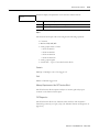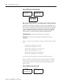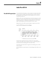
1
Pico GFX-70
Controllers
Bulletin 1760
User Manual
Important User Information
Solid state equipment has operational characteristics differing from those of
electromechanical equipment. Safety Guidelines for the Application,
Installation and Maintenance of Solid State Controls (Publication SGI-1.1
available from your local Rockwell Automation sales office or online at
http://www.ab.com/manuals/gi) describes some important differences
between solid state equipment and hard-wired electromechanical devices.
Because of this difference, and also because of the wide variety of uses for
solid state equipment, all persons responsible for applying this equipment
must satisfy themselves that each intended application of this equipment is
acceptable.
In no event will Rockwell Automation, Inc. be responsible or liable for
indirect or consequential damages resulting from the use or application of
this equipment.
The examples and diagrams in this manual are included solely for illustrative
purposes. Because of the many variables and requirements associated with
any particular installation, Rockwell Automation, Inc. cannot assume
responsibility or liability for actual use based on the examples and diagrams.
No patent liability is assumed by Rockwell Automation, Inc. with respect to
use of information, circuits, equipment, or software described in this manual.
Reproduction of the contents of this manual, in whole or in part, without
written permission of Rockwell Automation, Inc. is prohibited.
Throughout this manual we use notes to make you aware of safety
considerations.
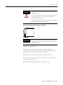
WARNING
IMPORTANT
ATTENTION
Identifies information about practices or circumstances
that can cause an explosion in a hazardous environment,
which may lead to personal injury or death, property
damage, or economic loss.
Identifies information that is critical for successful
application and understanding of the product.
Identifies information about practices or circumstances
that can lead to personal injury or death, property
damage, or economic loss. Attentions help you:
• identify a hazard
• avoid a hazard
• recognize the consequence
SHOCK HAZARD
Labels may be located on or inside the drive to alert
people that dangerous voltage may be present.
BURN HAZARD
Labels may be located on or inside the drive to alert
people that surfaces may be dangerous temperatures.
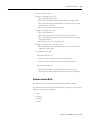
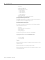
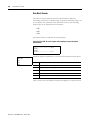
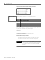
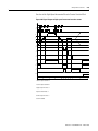
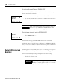
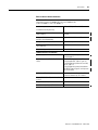
Summary of Changes
The information below summarizes the changes to this manual since the last
release as publication 1760-UM002A-EN-P, April 2004.
To help you locate new and updated information in this release of the manual,
we have included change bars as shown to the right of this paragraph.
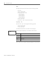
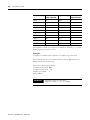
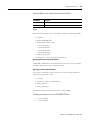
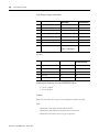
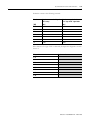
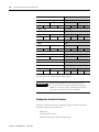
Catalog Number Release
History
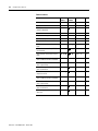
The following table shows the history of the Pico GFX-70 catalog numbers.
Released April 2004
GFX I/O Modules
1760-IB12XOW4IF
1760-IB12XOW4IOF
1760-IB12XOB4IF
1760-IB12XOB4IOF
Expansion I/O Modules
1760-IA12XOW6I
1760-IB12XOB8
1760-OW2
Processor Units
1760-LDF
1760-LDFC
Released April 2005
1760-IA12XOW4I
1760-IB12XOW6I
1760-LDFA
1760-LDFCA
1760-RM-GFX
Programming Software and Cable
1760-PICOSOFTPRO
1760-CBL-PC02
1760-PICOPRO-PC02
Display Units
1760-DUB
1760-DU
Memory Module
1760-MM3
Power Supply
1606-XLP30E
Point-to-Point Serial Interface Cables
1760-CBL-2M
1760-CBL-5M
Cables for Pico-Link between Processors
1760-CBL-INT01
1760-CBL-INT03
1760-CBL-INT05
1760-CBL-INT300
1760-CONN-RJ45
1760-TERM1
3
Publication 1760-UM002B-EN-P - March 2005
Summary of Changes
4
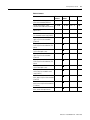
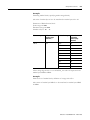
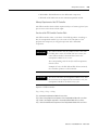
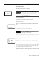
Released April 2004
Protective Covers
1760-NDM
1760-NDC
Mounting Feet
1760-NMF
Tools
1492-N90
1492-KWC
New Information
Released April 2005
The following table lists the sections of this manual where new information
has been added.
For this New Information
See
Added Figure 1.3, Remote Processor Features.
1-5
Revised Catalog Number Reference section to include new catalog numbers. 1-6
Publication 1760-UM002B-EN-P - March 2005
Revised Setting Values section.
1-19
In the section, Connecting the Expansion Unit, added a note that you can
only connect one expansion I/O module to each controller.
2-16
Modified text below Figure 2.28, Temperature sensor, brightness sensor, 20
mA sensor.
2-26
Added new catalog numbers to Table 2.47, Pico Expansion I/O Modules.
2-40
Added Installing the Remote Processor section.
2-41
Re-arranged the numbered steps within the Starting Point Status Display
section.
3-5
Added TIP on how to reinitialize the display.
3-32
Added IMPORTANT note about only writing the markers once.
4-14
Modified text in the High-Speed Functions section.
4-74
Added IMPORTANT in the Function of the GET Function Block section.
4-106
Modified text within the Function of the Year Time Switch Function Block
section.
4-113
Added text within the Accuracy section.
4-130
Modified text within the IMPORTANT statement.
4-135
Changed value for seconds time range in Table 4.65, Time Range.
4-141
Modified and added text within the Variable Setpoint Values section.
4-142
Modified title for Figure 4.68, Signal diagram of timing relay, off-delayed
(with/without random switching with/without retriggering).
4-146
Modified title for Figure 4.69, Signal diagram of timing relay, off-delayed
(with/without random switching with/without retriggering).
4-147
Totally new version of Chapter 5, Visualization with Pico GFX-70.
5-1
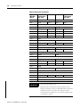
Summary of Changes
5
For this New Information
See
Modified text within the Memory Module section.
8-11
Modified text within the PicoSoft Pro section.
8-15
Modified the Device Version section.
8-17
Corrected dimension specifications and added new catalog numbers to
tables.
A-2
Revised Figure A.1, Dimensions of the 1760-DU and 1760-DUB
display/keypad.
A-3
Revised Figure A.4, Dimensions of the 1760-LDF… processor units.
A-4
Added Figure A.6, Dimensions of the 1760-RM… Remote Processor
modules.
A-4
Revised Table A.6, General Ambient Conditions.
A-5 and A-6
Revised Table A.7, Display/keypad Specifications.
A-7
Revised Table A.8, Power Supply Specifications for DC Processors.
A-8
Added new catalog number and footnote to Table A.10, GFX I/O Modules
Input Specifications.
A-10
Added new catalog number to Table A.11, GFX I/O Modules Relay Output
Specifications.
A-11
Modified some of the text in Table A.18, Function Block Definitions.
A-17
Publication 1760-UM002B-EN-P - March 2005
Summary of Changes
6
Publication 1760-UM002B-EN-P - March 2005
Table of Contents
Summary of Changes
Catalog Number Release History . . . . . . . . . . . . . . . . . . . . . . . . . . soc-3
New Information . . . . . . . . . . . . . . . . . . . . . . . . . . . . . . . . . . . . . . . soc-4
Preface
Who Should Use this Manual . . . . . . . . . . . . . . . . . . . . . . . . . . . . . . .
Purpose of this Manual . . . . . . . . . . . . . . . . . . . . . . . . . . . . . . . . . . . .
Common Techniques Used in this Manual. . . . . . . . . . . . . . . . . . . . .
Related Documentation . . . . . . . . . . . . . . . . . . . . . . . . . . . . . . . . . . . .
P-1
P-1
P-1
P-2
Chapter 1
Overview
Intended Use . . . . . . . . . . . . . . . . . . . . . . . . . . . . . . . . . . . . . . . . . . . . 1-1
Improper Use . . . . . . . . . . . . . . . . . . . . . . . . . . . . . . . . . . . . . . . . . 1-1
Product Description. . . . . . . . . . . . . . . . . . . . . . . . . . . . . . . . . . . . . . . 1-2
Component Features . . . . . . . . . . . . . . . . . . . . . . . . . . . . . . . . . . . . . . 1-4
Catalog Number Reference . . . . . . . . . . . . . . . . . . . . . . . . . . . . . . . . . 1-6
Pico GFX-70 Operation . . . . . . . . . . . . . . . . . . . . . . . . . . . . . . . . . . . 1-8
Buttons . . . . . . . . . . . . . . . . . . . . . . . . . . . . . . . . . . . . . . . . . . . . . . 1-8
Moving Through Menus and Choosing Values . . . . . . . . . . . . . . 1-8
Selecting Main and System Menu . . . . . . . . . . . . . . . . . . . . . . . . . 1-9
Pico GFX-70 LED Display. . . . . . . . . . . . . . . . . . . . . . . . . . . . . 1-11
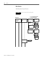
Menu Structure. . . . . . . . . . . . . . . . . . . . . . . . . . . . . . . . . . . . . . . 1-12
Selecting or Toggling Between Menu Items. . . . . . . . . . . . . . . . 1-18
Cursor Display . . . . . . . . . . . . . . . . . . . . . . . . . . . . . . . . . . . . . . . 1-18
Setting Values. . . . . . . . . . . . . . . . . . . . . . . . . . . . . . . . . . . . . . . . 1-19
Chapter 2
Installation
1
Mounting . . . . . . . . . . . . . . . . . . . . . . . . . . . . . . . . . . . . . . . . . . . . . . . 2-1
Connecting the Expansion Unit . . . . . . . . . . . . . . . . . . . . . . . . . . . . 2-16
Terminals . . . . . . . . . . . . . . . . . . . . . . . . . . . . . . . . . . . . . . . . . . . . . . 2-16
Tool for Cage Clamp Terminals . . . . . . . . . . . . . . . . . . . . . . . . . 2-16
Connection Cross-Sections of the
Cage Clamp Terminal Cables . . . . . . . . . . . . . . . . . . . . . . . . . . . 2-16
Tool for Slot-Head Screws for Expansion I/O Unit. . . . . . . . . 2-16
Connection Cross-Sections of Screw Terminal Cables . . . . . . . 2-16
Connecting the Power Supply . . . . . . . . . . . . . . . . . . . . . . . . . . . . . . 2-17
Cable Protection . . . . . . . . . . . . . . . . . . . . . . . . . . . . . . . . . . . . . 2-19
Connecting the Inputs . . . . . . . . . . . . . . . . . . . . . . . . . . . . . . . . . . . . 2-20
Connecting AC Inputs. . . . . . . . . . . . . . . . . . . . . . . . . . . . . . . . . 2-20
Connecting DC Inputs . . . . . . . . . . . . . . . . . . . . . . . . . . . . . . . . 2-23
Connecting the Outputs. . . . . . . . . . . . . . . . . . . . . . . . . . . . . . . . . . . 2-28
Connecting Relay Outputs. . . . . . . . . . . . . . . . . . . . . . . . . . . . . . . . . 2-28
1760-IB12XOW4IF, 1760-IB12XOW4IOF . . . . . . . . . . . . . . . 2-28
1760-IA12XOW6I . . . . . . . . . . . . . . . . . . . . . . . . . . . . . . . . . . . . 2-29
1760-OW2 . . . . . . . . . . . . . . . . . . . . . . . . . . . . . . . . . . . . . . . . . . 2-29
Connecting Transistor Outputs. . . . . . . . . . . . . . . . . . . . . . . . . . . . . 2-30
1760-IB12XOB4IF, 1760-IB12XOB4IOF . . . . . . . . . . . . . . . . 2-30
Publication 1760-UM002B-EN-P - March 2005
Table of Contents
2
1760-IB12XOB8 . . . . . . . . . . . . . . . . . . . . . . . . . . . . . . . . . . . . .
Connecting Analog Outputs . . . . . . . . . . . . . . . . . . . . . . . . . . . . . . .
Connecting Servo Valves. . . . . . . . . . . . . . . . . . . . . . . . . . . . . . .
Setpoint Entry for a Drive. . . . . . . . . . . . . . . . . . . . . . . . . . . . . .
Connecting the Pico-Link . . . . . . . . . . . . . . . . . . . . . . . . . . . . . . . . .
Accessories . . . . . . . . . . . . . . . . . . . . . . . . . . . . . . . . . . . . . . . . . .
Cable Length and Cross-Sections . . . . . . . . . . . . . . . . . . . . . . . .
Plugging and Unplugging Network Cables. . . . . . . . . . . . . . . . .
Connecting the Serial Interface . . . . . . . . . . . . . . . . . . . . . . . . . . . . .
Expanding Inputs/Outputs . . . . . . . . . . . . . . . . . . . . . . . . . . . . . . . .
Local Expansion . . . . . . . . . . . . . . . . . . . . . . . . . . . . . . . . . . . . .
Remote Expansion. . . . . . . . . . . . . . . . . . . . . . . . . . . . . . . . . . . .
Installing the Remote Processor . . . . . . . . . . . . . . . . . . . . . . . . . . . .
Mounting and Removal . . . . . . . . . . . . . . . . . . . . . . . . . . . . . . . .
Making Connections . . . . . . . . . . . . . . . . . . . . . . . . . . . . . . . . . .
2-30
2-32
2-32
2-33
2-33
2-33
2-35
2-36
2-38
2-40
2-40
2-41
2-41
2-41
2-42
Chapter 3
Commissioning
Switching On . . . . . . . . . . . . . . . . . . . . . . . . . . . . . . . . . . . . . . . . . . . . 3-1
Setting the Menu Language . . . . . . . . . . . . . . . . . . . . . . . . . . . . . . . . . 3-1
Operating Modes . . . . . . . . . . . . . . . . . . . . . . . . . . . . . . . . . . . . . . . . . 3-2
Creating your First Circuit Diagram . . . . . . . . . . . . . . . . . . . . . . . . . . 3-3
Starting Point Status Display . . . . . . . . . . . . . . . . . . . . . . . . . . . . . 3-5
Circuit Diagram Display . . . . . . . . . . . . . . . . . . . . . . . . . . . . . . . . 3-6
From the First Contact to the Output Coil . . . . . . . . . . . . . . . . . 3-7
Wiring . . . . . . . . . . . . . . . . . . . . . . . . . . . . . . . . . . . . . . . . . . . . . . . 3-8
Testing the Circuit Diagram . . . . . . . . . . . . . . . . . . . . . . . . . . . . 3-10
Deleting the Circuit Diagram . . . . . . . . . . . . . . . . . . . . . . . . . . . 3-13
Fast Circuit Diagram Entry . . . . . . . . . . . . . . . . . . . . . . . . . . . . . 3-13
Configuring a Pico-Link Network. . . . . . . . . . . . . . . . . . . . . . . . . . . 3-14
Entering the Network Station Number . . . . . . . . . . . . . . . . . . . 3-15
Entering Network Stations . . . . . . . . . . . . . . . . . . . . . . . . . . . . . 3-16
Configuring a Pico-Link Network . . . . . . . . . . . . . . . . . . . . . . . 3-17
Changing the Pico-Link Configuration. . . . . . . . . . . . . . . . . . . . 3-18
Displaying the Status Display of Other Stations . . . . . . . . . . . . 3-18
Configuring the Connection for the Terminal Mode . . . . . . . . . . . . 3-20
Setting up the Serial Interface . . . . . . . . . . . . . . . . . . . . . . . . . . . 3-21
Terminal Mode . . . . . . . . . . . . . . . . . . . . . . . . . . . . . . . . . . . . . . . . . . 3-25
Chapter 4
Wiring with Pico GFX-70
Publication 1760-UM002B-EN-P - March 2005
Pico GFX-70 Operation . . . . . . . . . . . . . . . . . . . . . . . . . . . . . . . . . . . 4-1
Buttons for Drawing Circuit Diagrams and
Function Block Usage . . . . . . . . . . . . . . . . . . . . . . . . . . . . . . . . . . 4-1
Operating Principles . . . . . . . . . . . . . . . . . . . . . . . . . . . . . . . . . . . 4-2
Usable Relays and Function Blocks (coils) . . . . . . . . . . . . . . . . . . 4-9
Markers, Analog Operands . . . . . . . . . . . . . . . . . . . . . . . . . . . . . 4-12
Table of Contents
3
Number Formats . . . . . . . . . . . . . . . . . . . . . . . . . . . . . . . . . . . . . 4-15
Circuit Diagram Display . . . . . . . . . . . . . . . . . . . . . . . . . . . . . . . 4-15
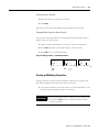
Saving and Loading Programs. . . . . . . . . . . . . . . . . . . . . . . . . . . 4-17
Working with Contacts and Relays . . . . . . . . . . . . . . . . . . . . . . . . . . 4-18
Creating and Modifying Connections . . . . . . . . . . . . . . . . . . . . . 4-21
Inserting and Deleting a Circuit Connection . . . . . . . . . . . . . . . 4-23
Saving Circuit Diagrams . . . . . . . . . . . . . . . . . . . . . . . . . . . . . . . 4-24
Aborting Circuit Diagram Entry . . . . . . . . . . . . . . . . . . . . . . . . . 4-24
Searching for Contacts and Coils . . . . . . . . . . . . . . . . . . . . . . . . 4-24
“Go To” a Circuit Connection . . . . . . . . . . . . . . . . . . . . . . . . . . 4-25
Deleting the Circuit Connection . . . . . . . . . . . . . . . . . . . . . . . . 4-25
Switching Via the Cursor Buttons. . . . . . . . . . . . . . . . . . . . . . . . 4-26
Checking the Circuit Diagram. . . . . . . . . . . . . . . . . . . . . . . . . . . 4-27
Function Block Editor. . . . . . . . . . . . . . . . . . . . . . . . . . . . . . . . . 4-28
Checking Function Blocks. . . . . . . . . . . . . . . . . . . . . . . . . . . . . . 4-32
Coil Functions . . . . . . . . . . . . . . . . . . . . . . . . . . . . . . . . . . . . . . . 4-33
Function Blocks . . . . . . . . . . . . . . . . . . . . . . . . . . . . . . . . . . . . . . . . . 4-38
Analog Value Comparator/Threshold Value Switch . . . . . . . . . 4-40
Arithmetic Function Block . . . . . . . . . . . . . . . . . . . . . . . . . . . . . 4-43
Data Block Comparator. . . . . . . . . . . . . . . . . . . . . . . . . . . . . . . . 4-47
Data Block Transfer. . . . . . . . . . . . . . . . . . . . . . . . . . . . . . . . . . . 4-54
Boolean Operations . . . . . . . . . . . . . . . . . . . . . . . . . . . . . . . . . . . 4-64
Counters . . . . . . . . . . . . . . . . . . . . . . . . . . . . . . . . . . . . . . . . . . . . 4-68
High-Speed Functions . . . . . . . . . . . . . . . . . . . . . . . . . . . . . . . . . 4-74
Frequency Counters. . . . . . . . . . . . . . . . . . . . . . . . . . . . . . . . . . . 4-75
High-Speed Counters. . . . . . . . . . . . . . . . . . . . . . . . . . . . . . . . . . 4-79
High-Speed Incremental Encoder Counters . . . . . . . . . . . . . . . 4-85
Comparators. . . . . . . . . . . . . . . . . . . . . . . . . . . . . . . . . . . . . . . . . 4-90
Text Output Function Block. . . . . . . . . . . . . . . . . . . . . . . . . . . . 4-92
Data Function Block . . . . . . . . . . . . . . . . . . . . . . . . . . . . . . . . . . 4-93
PID Controller . . . . . . . . . . . . . . . . . . . . . . . . . . . . . . . . . . . . . . . 4-95
Signal Smoothing Filter . . . . . . . . . . . . . . . . . . . . . . . . . . . . . . . 4-101
GET, Fetch a Value from the Network . . . . . . . . . . . . . . . . . . 4-104
Seven-Day Time Switch. . . . . . . . . . . . . . . . . . . . . . . . . . . . . . . 4-106
Year Time Switch. . . . . . . . . . . . . . . . . . . . . . . . . . . . . . . . . . . . 4-111
Value Scaling . . . . . . . . . . . . . . . . . . . . . . . . . . . . . . . . . . . . . . . 4-115
Jumps . . . . . . . . . . . . . . . . . . . . . . . . . . . . . . . . . . . . . . . . . . . . . 4-119
Master Reset. . . . . . . . . . . . . . . . . . . . . . . . . . . . . . . . . . . . . . . . 4-122
Numerical Converters . . . . . . . . . . . . . . . . . . . . . . . . . . . . . . . . 4-123
Operating Hours Counter . . . . . . . . . . . . . . . . . . . . . . . . . . . . . 4-129
PUT, Send a Value onto the Network . . . . . . . . . . . . . . . . . . . 4-130
Pulse Width Modulation . . . . . . . . . . . . . . . . . . . . . . . . . . . . . . 4-132
Setting Date/Time . . . . . . . . . . . . . . . . . . . . . . . . . . . . . . . . . . . 4-135
Set Cycle Time . . . . . . . . . . . . . . . . . . . . . . . . . . . . . . . . . . . . . . 4-137
Timing Relay . . . . . . . . . . . . . . . . . . . . . . . . . . . . . . . . . . . . . . . 4-139
Value Limitation. . . . . . . . . . . . . . . . . . . . . . . . . . . . . . . . . . . . . 4-152
Publication 1760-UM002B-EN-P - March 2005
Table of Contents
4
Example with Timing Relay and Counter Function Block . . . 4-154
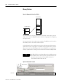
Chapter 5
Visualization with Pico GFX-70
Screens . . . . . . . . . . . . . . . . . . . . . . . . . . . . . . . . . . . . . . . . . . . . . . . . . 5-1
Memory Division . . . . . . . . . . . . . . . . . . . . . . . . . . . . . . . . . . . . . . 5-2
Western European Character Table . . . . . . . . . . . . . . . . . . . . . . . 5-3
Screen Overview. . . . . . . . . . . . . . . . . . . . . . . . . . . . . . . . . . . . . . . . . . 5-5
Screen Editor . . . . . . . . . . . . . . . . . . . . . . . . . . . . . . . . . . . . . . . . . . . . 5-6
Static Text. . . . . . . . . . . . . . . . . . . . . . . . . . . . . . . . . . . . . . . . . . . . 5-6
Bit Display . . . . . . . . . . . . . . . . . . . . . . . . . . . . . . . . . . . . . . . . . . . 5-9
Date and Time . . . . . . . . . . . . . . . . . . . . . . . . . . . . . . . . . . . . . . . 5-12
Bitmap . . . . . . . . . . . . . . . . . . . . . . . . . . . . . . . . . . . . . . . . . . . . . 5-15
Numerical Value . . . . . . . . . . . . . . . . . . . . . . . . . . . . . . . . . . . . . 5-19
Value Entry . . . . . . . . . . . . . . . . . . . . . . . . . . . . . . . . . . . . . . . . . 5-25
Message Text . . . . . . . . . . . . . . . . . . . . . . . . . . . . . . . . . . . . . . . . 5-30
Button Editor . . . . . . . . . . . . . . . . . . . . . . . . . . . . . . . . . . . . . . . . . . . 5-37
Select an Operable Screen Element . . . . . . . . . . . . . . . . . . . . . . 5-37
Display Backlight . . . . . . . . . . . . . . . . . . . . . . . . . . . . . . . . . . . . . 5-37
Screen Change . . . . . . . . . . . . . . . . . . . . . . . . . . . . . . . . . . . . . . . 5-37
Password Logout . . . . . . . . . . . . . . . . . . . . . . . . . . . . . . . . . . . . . 5-38
Set Variable to Fixed Value . . . . . . . . . . . . . . . . . . . . . . . . . . . . . 5-38
Increment Variable . . . . . . . . . . . . . . . . . . . . . . . . . . . . . . . . . . . 5-38
Decrement Variable . . . . . . . . . . . . . . . . . . . . . . . . . . . . . . . . . . . 5-38
Changeover Relay . . . . . . . . . . . . . . . . . . . . . . . . . . . . . . . . . . . . 5-38
Chapter 6
Pico-Link and Point-to-Point
Serial Connections
Publication 1760-UM002B-EN-P - March 2005
Introduction to Pico-Link . . . . . . . . . . . . . . . . . . . . . . . . . . . . . . . . . . 6-1
Pico-Link Topologies, Addressing and Functions . . . . . . . . . . . . . . . 6-2
Loop Through the Unit Wiring Method. . . . . . . . . . . . . . . . . . . . 6-2
T-Connector and Spur Line . . . . . . . . . . . . . . . . . . . . . . . . . . . . . 6-2
Topology and Addressing Examples . . . . . . . . . . . . . . . . . . . . . . 6-3
Position and Addressing of the Operands via the Pico-Link . . . 6-4
Functions of the Stations in the Network . . . . . . . . . . . . . . . . . . 6-6
Possible Write and Read Authorization in the Network . . . . . . . 6-6
Configuring the Pico-Link . . . . . . . . . . . . . . . . . . . . . . . . . . . . . . . . . . 6-7
Station Number . . . . . . . . . . . . . . . . . . . . . . . . . . . . . . . . . . . . . . . 6-7
Transmission Speed . . . . . . . . . . . . . . . . . . . . . . . . . . . . . . . . . . . . 6-7
Pause Time, Changing the Write Repetition Rate Manually . . . . 6-8
Send Each Change on the Inputs/Outputs (SEND IO). . . . . . . 6-9
Automatic Change of the RUN and STOP Mode . . . . . . . . . . . . 6-9
Input/Output Device (REMOTE IO) Configuration. . . . . . . . 6-10
Station Message Types. . . . . . . . . . . . . . . . . . . . . . . . . . . . . . . . . 6-11
Transfer Behavior . . . . . . . . . . . . . . . . . . . . . . . . . . . . . . . . . . . . 6-11
Signs of Life of the Individual Stations and Diagnostics . . . . . . 6-12
Network Transmission Security . . . . . . . . . . . . . . . . . . . . . . . . . 6-15
Table of Contents
5
Introduction to the Serial Interface . . . . . . . . . . . . . . . . . . . . . . . . . . 6-16
Topology . . . . . . . . . . . . . . . . . . . . . . . . . . . . . . . . . . . . . . . . . . . 6-16
Configuration of the Serial Interface . . . . . . . . . . . . . . . . . . . . . 6-18
Chapter 7
Pico GFX-70 Settings
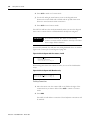
Password Protection . . . . . . . . . . . . . . . . . . . . . . . . . . . . . . . . . . . . . . 7-1
Password Setup . . . . . . . . . . . . . . . . . . . . . . . . . . . . . . . . . . . . . . . 7-2
Selecting the Scope of the Password. . . . . . . . . . . . . . . . . . . . . . . 7-3
Activating the Password . . . . . . . . . . . . . . . . . . . . . . . . . . . . . . . . 7-4
Unlocking Pico GFX-70 . . . . . . . . . . . . . . . . . . . . . . . . . . . . . . . . 7-5
Changing or Deleting the Password Range . . . . . . . . . . . . . . . . . 7-6
Changing the Menu Language . . . . . . . . . . . . . . . . . . . . . . . . . . . . . . . 7-8
Changing Parameters . . . . . . . . . . . . . . . . . . . . . . . . . . . . . . . . . . . . . . 7-9
Adjustable Parameters for Function Blocks . . . . . . . . . . . . . . . . 7-10
Setting Date, Time and Daylight Savings Time . . . . . . . . . . . . . . . . 7-11
Changing Between Winter/Summer time (DST) . . . . . . . . . . . . . . . 7-12
Selecting DST. . . . . . . . . . . . . . . . . . . . . . . . . . . . . . . . . . . . . . . . 7-13
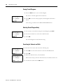
Activating Input Delay (debounce) . . . . . . . . . . . . . . . . . . . . . . . . . . 7-14
Deactivating Debounce (input delay) . . . . . . . . . . . . . . . . . . . . . 7-14
Activating and Deactivating the P Buttons. . . . . . . . . . . . . . . . . . . . 7-15
Activating the P Buttons . . . . . . . . . . . . . . . . . . . . . . . . . . . . . . . 7-15
Deactivating the P Buttons . . . . . . . . . . . . . . . . . . . . . . . . . . . . . 7-16
Startup Behavior. . . . . . . . . . . . . . . . . . . . . . . . . . . . . . . . . . . . . . . . . 7-16
Setting the Startup Behavior . . . . . . . . . . . . . . . . . . . . . . . . . . . . 7-16
Behavior When the Circuit Diagram is Deleted. . . . . . . . . . . . . 7-17
Behavior During Upload/Download to Module or PC . . . . . . 7-17
Possible Faults . . . . . . . . . . . . . . . . . . . . . . . . . . . . . . . . . . . . . . . 7-18
Card Startup Behavior . . . . . . . . . . . . . . . . . . . . . . . . . . . . . . . . . 7-18
Terminal Mode. . . . . . . . . . . . . . . . . . . . . . . . . . . . . . . . . . . . . . . 7-19
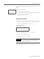
Setting LCD Contrast and Backlight. . . . . . . . . . . . . . . . . . . . . . . . . 7-20
Retention . . . . . . . . . . . . . . . . . . . . . . . . . . . . . . . . . . . . . . . . . . . . . . 7-22
Requirements . . . . . . . . . . . . . . . . . . . . . . . . . . . . . . . . . . . . . . . . 7-23
Setting Retentive Behavior . . . . . . . . . . . . . . . . . . . . . . . . . . . . . 7-23
Deleting Ranges . . . . . . . . . . . . . . . . . . . . . . . . . . . . . . . . . . . . . . 7-24
Deleting Retentive Actual Values of
Markers and Function Blocks . . . . . . . . . . . . . . . . . . . . . . . . . . . 7-24
Transferring Retentive Behavior . . . . . . . . . . . . . . . . . . . . . . . . . 7-24
Displaying Device Information . . . . . . . . . . . . . . . . . . . . . . . . . . . . . 7-25
Chapter 8
Inside Pico GFX-70
Pico GFX-70 Program Cycle. . . . . . . . . . . . . . . . . . . . . . . . . . . . . . . .
Evaluation of the High-Speed Counters CF, CH and CI . . . . . .
Memory Management of the Pico GFX-70 . . . . . . . . . . . . . . . . .
Delay Times for Inputs and Outputs . . . . . . . . . . . . . . . . . . . . . . . . .
Delay Times for the GFX Inputs . . . . . . . . . . . . . . . . . . . . . . . . .
8-1
8-4
8-4
8-5
8-5
Publication 1760-UM002B-EN-P - March 2005
Table of Contents
6
Monitoring of Short-Circuit and Overload with 1760-IB12XOB8 . . 8-7
Examples . . . . . . . . . . . . . . . . . . . . . . . . . . . . . . . . . . . . . . . . . . . . 8-7
Expanding Pico GFX-70 . . . . . . . . . . . . . . . . . . . . . . . . . . . . . . . . . . . 8-8
How is an Expansion Unit Recognized? . . . . . . . . . . . . . . . . . . . 8-8
Transfer Behavior . . . . . . . . . . . . . . . . . . . . . . . . . . . . . . . . . . . . . 8-9
Function Monitoring of Expansion Units . . . . . . . . . . . . . . . . . . 8-9
QA Analog Output . . . . . . . . . . . . . . . . . . . . . . . . . . . . . . . . . . . . . . 8-10
Loading and Saving Programs . . . . . . . . . . . . . . . . . . . . . . . . . . . . . . 8-10
GFX without Display and Keypad . . . . . . . . . . . . . . . . . . . . . . . 8-10
Interface . . . . . . . . . . . . . . . . . . . . . . . . . . . . . . . . . . . . . . . . . . . . 8-10
Memory Module. . . . . . . . . . . . . . . . . . . . . . . . . . . . . . . . . . . . . . 8-11
PicoSoft Pro . . . . . . . . . . . . . . . . . . . . . . . . . . . . . . . . . . . . . . . . . 8-15
Device Version . . . . . . . . . . . . . . . . . . . . . . . . . . . . . . . . . . . . . . . . . . 8-17
Appendix A
Specifications
General . . . . . . . . . . . . . . . . . . . . . . . . . . . . . . . . . . . . . . . . . . . . . . . . A-1
List of the Function Blocks . . . . . . . . . . . . . . . . . . . . . . . . . . . . . . . A-17
Memory Requirement . . . . . . . . . . . . . . . . . . . . . . . . . . . . . . . . . . . A-20
Index
Publication 1760-UM002B-EN-P - March 2005
Preface
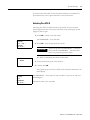
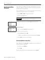
Read this preface to familiarize yourself with the rest of the manual. It provides
information concerning:
•
•
•
•
Who Should Use this
Manual
who should use this manual
the purpose of this manual
conventions used in this manual
related documentation
Use this manual if you are responsible for designing, installing, programming,
or troubleshooting automation control systems that use Allen-Bradley Pico
controllers.
Pico GFX-70 must only be installed and wired by trained electricians or other
persons familiar with the installation of electrical equipment.
You should have a basic understanding of electrical circuitry and familiarity
with relay logic. You should understand electronic process control and be able
to interpret the ladder logic instructions required to generate the electronic
signals that control your application.
If you do not, contact your local Allen-Bradley representative for the proper
training before using this product.
Purpose of this Manual
This manual is a learning and reference guide for Pico GFX-70 controller. It
contains the information you need to install, wire, and configure the module. It
also provides diagnostic and troubleshooting information and programming
examples
Common Techniques Used
in this Manual
The following conventions are used throughout this manual:
1
•
•
•
•
Bulleted lists such as this one provide information, not procedural steps.
Numbered lists provide sequential steps or hierarchical information.
Italic type is used for emphasis.
Text in bold type indicates words or phrases you should type
Publication 1760-UM002B-EN-P - March 2005
Preface
2
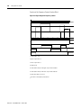
Related Documentation
The following documents contain information that may be helpful to you as
you use Allen-Bradley SLC products. If you would like a manual, you can:
• download a free electronic version from the internet:
• www.theautomationbookstore.com
• purchase a printed manual by:
– contacting your local distributor or Rockwell Automation
representative
– visiting www.theautomationbookstore.com and placing your
order
– calling 1.800.963.9548 (USA/Canada)
– or 001.330.725.1574 (Outside USA/Canada)
For
Read this Document
Document Number
Introduction to using PicoSoft Pro software
Pico GFX-70 Controllers Quick Start
1760-QS002A-EN-P
Installation and mounting procedures for the processor
Pico GFX-70 Processors Installation
Instructions
1760-IN004A-MU-P
Installation and mounting procedures for the display unit
Pico GFX-70 Display Units Installation
Instructions
1760-IN005A-MU-P
Installation and mounting procedures for the I/O modules
Pico GFX-70 I/O Modules Installation
Instructions
1760-IN006A-MU-P
Installation and mounting procedures for the serial interface cable
Pico GFX-70 Serial Interface Cable
Installation Instructions
1760-IN007A-MU-P
In-depth information on grounding and wiring Allen-Bradley
programmable controllers
Allen-Bradley Programmable Controller
Grounding and Wiring Guidelines
1770-4.1
A description of important differences between solid-state programmable Application Considerations for
controller products and hard-wired electromechanical devices
Solid-State Controls
SGI-1.1
An article on wire sizes and types for grounding electrical equipment
National Electrical Code - Published by the National Fire
Protection Association of Boston, MA.
A complete listing of current documentation, including ordering
instructions. Also indicates whether the documents are available on
CD-ROM or in multi-languages.
Allen-Bradley Publication Index
SD499
A glossary of industrial automation terms and abbreviations
Allen-Bradley Industrial Automation
Glossary
AG-7.1
Publication 1760-UM002B-EN-P - March 2005
Chapter
1
Overview
Intended Use
The Pico GFX-70 is a programmable device that provides HMI, switching,
closed-loop and open-loop control functions, and can be used to replace relay
and contactor controls. All components must be properly installed before use.
The display and keypad of the are protected to IP65 and do not normally
require any special housing protection. The rear components are designed as
mounting units and must be installed in an enclosure, control cabinet or a
service distribution board. Both the power feed and the signal terminals must
be laid and covered so as to prevent accidental contact.
The installation must comply with regulations for electromagnetic
compatibility (EMC).
Power up must not cause any hazards arising from activated devices, such as
unexpected motor startups or power ups.
Improper Use
Pico GFX-70 should not be used as a substitute for safety-related controls
such as burner or crane controls, emergency-stop or two-hand safety controls.
1
Publication 1760-UM002B-EN-P - March 2005
1-2
Overview
Product Description
The Pico GFX-70 is an electronic HMI unit and control relay with the
following features:
•
•
•
•
•
•
Logic functions
Timing relay and counter functions
Time switch functions
Arithmetic functions
PID controllers
Operator and display functions
The Pico GFX-70 is a display, HMI, control and input device in one. It allows
you to create solutions for domestic applications as well as tasks in machine
and plant construction. It is a modular and flexible device.
The Pico-Link enables the connection of up to eight stations to form a single
control system. Each station can contain a program. This allows the design of
systems using high-speed controllers with decentralized intelligence.
In Terminal mode, the Pico GFX-70 can be used to control any device in the
network and display data from it. In this mode, the Pico GFX-70 makes its
keypad and display available to the other device for use.
Two Pico GFX-70 devices can be connected simply via the serial interfaces.
Circuit diagrams are connected up using ladder diagrams, and each element is
entered directly via the Pico GFX-70 display. For example, you can:
• connect make and break contacts in series and in parallel
• switch output relays and auxiliary contacts
• define outputs as coils, impulse relays, rising or falling edge-triggered
relays or as latching relays
• select timing relays with different functions:
– on-delayed
– on-delayed with random switching
– off-delayed
– off-delayed with random switching
– on and off delayed
– on and off delayed with random switching
– on and off delayed with random switching
– single pulse
– synchronous flashing
– asynchronous flashing
• use up and down counters
• count high-speed signals:
– up and down counters with upper and lower limit values
Publication 1760-UM002B-EN-P - March 2005
Overview
•
•
•
•
•
•
•
•
•
•
•
•
•
1-3
– preset
– frequency counters
– high-speed counters
– count incremental encoder values
compare values
display graphics, texts, variables, enter set points, display flashing values
and graphics, change and replace graphics and texts by push button
process additional inputs and outputs
use 7-day and year time switches
count operating hours (operating hours counter)
communicate via the Pico-Link
set up point-to-point communication via the serial interface
provide closed-loop control with P, PI and PID controllers
scale arithmetic values
output manipulated variables as pulse-width modulated signals
run arithmetic functions:
– add
– subtract
– multiply
– divide
track the flow of current in the circuit diagram
load, save and password-protect circuit diagrams
If you prefer to wire up the Pico GFX-70 from a PC, then use Pico Soft Pro.
Pico Soft Pro allows you to create and test your circuit diagram on the PC. All
display and operator functions on the device are created exclusively using the
Pico Soft Pro software. Pico Soft Pro is also used to print out your circuit
diagram in DIN, ANSI or ladder format.
Publication 1760-UM002B-EN-P - March 2005
1-4
Overview
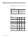
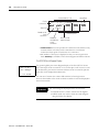
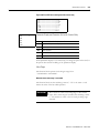
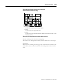
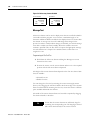
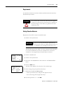
Component Features
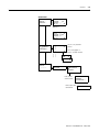
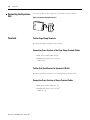
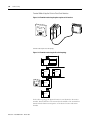
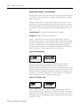
Figure 1.1 Display and Keypad Features
1
2
3
4
9
8
7
6
5
1. DEL button
2. Graphic display
3. ALT button
4. LEDs for signalling
5. Mode button
6. Right, down cursor buttons
7. OK button
8. Left, up cursor buttons
9. ESC button
Publication 1760-UM002B-EN-P - March 2005
Overview
1-5
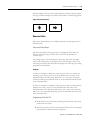
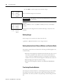
Processor
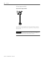
Figure 1.2 Processor Features
1
2
6
5
3
4
1. Power supply
2. Pico-Link terminals
3. Expansion module connector
4. Socket for memory module, PC and point-to-point connection
5. Power supply / operating mode LED
6. Pico-Link LED
Figure 1.3 Remote Processor Features
1
2
1. 24V dc Voltage supply
2. Interface (with cover) Terminal for connecting cable
Publication 1760-UM002B-EN-P - March 2005
1-6
Overview
I/O Modules
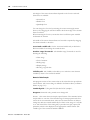
Figure 1.4 I/O Module Features
1
2
3
1. Inputs
2. Analog output (optional)
3. Outputs
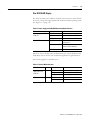
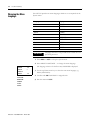
Catalog Number Reference
Table 1.1 Pico GFX-70 Catalog Number Listing
Catalog Number
Description
GFX I/O Modules
1760-IA12XOW4I
(12) 120/240V ac inputs, (4) relay output, analog input
1760-IB12XOW4IF
(12) 24V dc inputs, (4) relay output, analog input
1760-IB12XOW4IOF
(12) 24V dc inputs, (4) relay outputs, analog input and output
1760-IB12XOB4IF
(12) 24V dc inputs, (4) transistor outputs, analog input
1760-IB12XOB4IOF
(12) 24V dc inputs, (4) transistor outputs, analog input and output
Expansion I/O Modules
1760-IA12XOW6I
(12) 120/240V ac inputs, (6) relay outputs
1760-IB12XOB8
(12) 24V dc inputs, (8) transistor outputs
1760-IB12XOW6I
(12) 24V dc inputs, (6) relay outputs
1760-OW2
(2) relay outputs
Processor Units
1760-LDF
DC Processor
1760-LDFC
DC Processor with Pico-Link Terminal
1760-LDFA
AC Processor
1760-LDFCA
AC Processor with Pico-Link Terminal
1760-RM-GFX
Remote Processor
Programming Software and Cable
1760-PICOSOFTPRO
PicoSoft Pro Programming Software
1760-CBL-PC02
Programming Cable, PC to Processor
Publication 1760-UM002B-EN-P - March 2005
Pieces per
Package
1
1
1
1
1
1
1
1
1
1
1
1
1
1
1
1
Overview
1-7
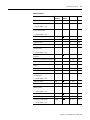
Table 1.1 Pico GFX-70 Catalog Number Listing
Catalog Number
Description
1760-PICOPRO-PC02
PicoSoft Pro Software and Cable Kit
Display Units
1760-DUB
Display Unit with Push buttons
1760-DU
Display Unit without Push buttons
Memory Module
1760-MM3
256K Memory Module
Power Supply
1606-XLP30E
DC Power Supply
Point-to-Point Serial Interface Cables
1760-CBL-2M
Point-to-Point Serial Interface Cable, 2m (6.6 ft)
1760-CBL-5M
Point-to-Point Serial Interface Cable, 5m (16.4 ft)
Cables for Pico-Link between Processors
1760-CBL-INT01
Pico-Link Cable, 0.3m (1 ft)
1760-CBL-INT03
Pico-Link Cable 0.8m (2.6 ft)
1760-CBL-INT05
Pico-Link Cable 1.5 m (5 ft)
1760-CBL-INT300
Pico-Link Cable, non-terminated, 100m (300 ft)
1760-CONN-RJ45
Connectors for Pico-Link Cable
1760-TERM1
Network Termination Resistor
Protective Covers
1760-NDM
Membrane Protect Display
1760-NDC
Cover Protect Display
Mounting Feet
1760-NMF
Mounting Feet (for panel mounting processors and I/O modules)
Tools
1492-N90
Screwdriver
1492-KWC
Wire Cutter
Pieces per
Package
1
1
1
1
1
1
1
5
3
2
1
2
2
1
1
8
5
1
Publication 1760-UM002B-EN-P - March 2005
1-8
Overview
Pico GFX-70 Operation
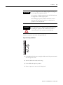
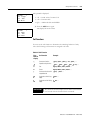
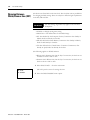
Buttons
ALT
DEL
DEL: Delete object in circuit diagram
ALT: Special functions in circuit-diagram, Status display
OK
ESC
*
Cursor buttons (up, down, left, right):
Move cursor
Select menu items
Set contact numbers, contacts and values
OK: Next menu level, Save your entry
ESC: Previous menu level, Cancel
*:Toggle between visualization display and Status display close Terminal mode
In visualization applications, the keypad can be used for
other functions than the ones stated above. In this case the
buttons are assigned the function selected in the
application. The standard button functions are only
restored when you leave the application.
TIP
Moving Through Menus and Choosing Values
DEL
and
ALT
OK
ESC
Show System menu
Go to next menu level
Select menu item
Activate, modify, save your entry
Return to last menu level
Cancel your entry since the last OK
up, down
Change menu item
Change value
left, right
Change place
Function of P buttons:
left
right
DEL
Publication 1760-UM002B-EN-P - March 2005
and
ESC
Input P1,
Input P3,
Reset the MFD display
up
down
Input P2
Input P4
Overview
1-9
Selecting Main and System Menu
Status Display
I .2..5.......
R.2
MO 02:00
RS
Q..34….
MO
S .2…6..
DEL
P-
and
ALT
STOP
No password
OK
Current selection
flashes in
the Pico GFX-70
menu
ESC
ESC
PROGRAM...
SECURITY...
SYSTEM...
MENU LANGUAGE
CONFIGURATOR...
STOP✓ RUN
PARAMETERS
SET CLOCK...
1st menu level
1st menu level
Main menu
System menu
Date display
I .2..5.......
ALT
P-
MO 11:50
Q..34....
STOP
I .2..5.......
PMO 01.04.2002
Q..34....
STOP
Pico GFX-70 Status Display
Inputs
Weekday/Time
Outputs
I 12.......... *
PMO 02:00
Q..34....
STOP
Display operating
mode, Terminal mode
or Weekday/Date
RUN/STOP/BUSY mode
On: 1, 2, 3, 4/Off:…
Publication 1760-UM002B-EN-P - March 2005
1-10
Overview
Status Display for Local Expansion
Inputs
Expansion
Weekday/Time
Outputs
R 1.........12
RS
AC
PMO 10:42
S 1......8 STOP
AC expansion ok/P buttons
or Weekday/Date
On: 1, 2, 3, 4/Off:…
RS = Expansion functioning correctly
Pico GFX-70 Advanced Status Display
Retention/Debounce/
Pico-Link station
Publication 1760-UM002B-EN-P - March 2005
I 12...6.89..12
RE
I NT1 AC PMO 14:42
T
Q 12345678
RUN
AC expansion ok/P buttons
Startup behavior
RE
Retention switched on
I
Debounce switched on
NT1
Pico-Link station with station address
COM
The COM connection is active
AC
AC expansion functioning correctly
DC
DC expansion functioning correctly
ST
When the power supply is switched on, Pico GFX-70 switches to STOP mode
Overview
1-11
Pico GFX-70 LED Display
Pico GFX-70 features two LEDs on the back of the processor. These indicate
the status of the power supply (POW) and the RUN or STOP operating mode
(See Figure 1.1 on page 1-4).
Table 1.2 Power Supply and RUN/STOP Operating Mode Indicators
LED
Status
Indicates
Power supply/RUN-STOP
mode LED
LED OFF
No power supply
LED continuously lit
Power supply present, STOP mode
LED flashing
Power supply present, RUN mode
LED OFF
Pico-Link not operational, fault, in
configuration
LED continuously lit
Pico-Link is initialized and no
station has been detected.
LED flashing
Pico-Link operating fault-free
Pico-Link LED
The front of the 1760-DU and 1760-DUB device has a green LED and a red
LED. These can be used in your visualization application as light indicators.
The following applies to Terminal mode:
Table 1.3 Terminal Mode Indicators
LED
Color
Status
Indicates
Power
supply/RUN-STOP
mode LED
Green
LED OFF
No power supply
Fault on the Pico-Link Red
LED continuously lit Power supply present, STOP mode
LED flashing
Power supply present, RUN mode
LED OFF
Operation correct
LED continuously lit Pico-Link remote device faulty
Publication 1760-UM002B-EN-P - March 2005
1-12
Overview
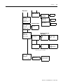
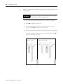
Menu Structure
Main Menu without Password Protection
Access the main menu by pressing OK.
TIP
STOP: Circuit diagram display
RUN: Power flow display
Main menu
PROGRAM..
. ▲
STOP ✓ RUN
PARAMETERS
SET CLOCK
▼
TERMINAL MODE..
PROGRAM...
CIRCUIT DIAGRAM
DELETE PROGRAM
CARD…
FUNCTION RELAYS
Parameter
display
Circuit diagram
SAVE ▲
▼
CANCEL ▲
Parameters
▼
SEARCH ▲
▼
GO TO ▲
▼
CIRCUIT DIAGRAM
FUNCTION RELAYS
Function block editor
Parameters
SAVE ▲
▼
CANCEL ▲
▼
SEARCH ▲
▼
GO TO ▲
▼
PROGRAM...
DELETE PROGRAM
CARD...
Publication 1760-UM002B-EN-P - March 2005
DELETE ?
Overview
1-13
Main menu
PROGRAM...
DELETE PROGRAM
DEVICE-CARD
CARD...
REPLACE ?
CARD-DEVICE
DELETE CARD ?
PROGRAM...
STOP
RUN
✓
▲
DEVICE-CARD
PARAMETERS
CARD-DEVICE
SET CLOCK... ▼
TERMINAL MODE
DELETE CARD ?
PROGRAM...
STOP
RUN
✓
▲
Parameter display
REPLACE ?
DEVICE-CARD
CARD-DEVICE
DELETE CARD ?
DELETE ?
Parameters
PARAMETERS
SET CLOCK... ▼
TERMINAL MODE..
Display for date and
time setting
PROGRAM...
▲
STOP
RUN ✓
PARAMETERS
SET CLOCK... ▼
SET CLOCK
TERMINAL MODE..
DST SETTING
HH:MM
DD.MM
YEAR
SET CLOCK
NONE ✓
DST SETTING
--:---.-____
MANUAL ✓
EU ✓
GB ✓
US ✓
HH:MM
DD.MM
YEAR
14:23
03.10
2001
SUMMERTIME START
DD.MM : --.-SUMMERTIME END
DD.MM : --.--
Only one selection is possible.
PROGRAM...
STOP
RUN ✓
PARAMETERS
SET CLOCK...
TERMINAL MODE..▼
▲
STATION ID: 0
START MODE
Connection
establishment
in progress...
Publication 1760-UM002B-EN-P - March 2005
1-14
Overview
Main Menu with Password Protection
Main menu
Unlocking
Pico GFX-70
PASSWORD... ▲
STOP RUN✓
PARAMETERS
SET CLOCK...
Password entry
Four wrong entries (if enabled)
DELETE ALL?
Password
▼
Correct entry
Status display
PASSWORD...
RUN
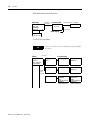
Pico GFX-70 System Menu
Access the system menu by simultaneously pressing DEL
and ALT.
TIP
Password
System
Password entry
SECURITY...
PASSWORD...
SYSTEM...
MENU LANGUAGE
CONFIGURATOR...
RANGE...
ACTIVATE PW
Change/
delete
Password
CHANGE PW
PASSWORD...
RANGE...
Publication 1760-UM002B-EN-P - March 2005
ENTER PASSWORD
------
ENTER PASSWORD
------
PROGRAM ✓
▲
PARAMETERS
TIME
OPERATING MODE▼
INTERFACE
DELETE FUNCTION
ACTIVATE PW
CHANGE PW
ACTIVATE PW
CHANGE PW
PROGRAM ✓
▲
PARAMETERS ✓
TIME ✓
OPERATINGMODE✓▼
INTERFACE ✓
DELETE FUNCTION✓
Overview
1-15
System menu
SECURITY...
SYSTEM...
MENU LANGUAGE
CONFIGURATOR...
DEBOUNCE ✓
P BUTTONS
RUN MODE
CARD MODE
TERMINAL MODE
DISPLAY...
RETENTION...
INFORMATION...
DEBOUNCE ✓
P BUTTONS
RUN MODE
CARD MODE
TERMINAL MODE
DISPLAY
▲
▼
DEBOUNCE ✓
▲
P BUTTONS ✓
RUN MODE ✓
CARD MODE ✓ ▼
TERMINAL MODE ✓
DISPLAY...
RETENTION...
INFORMATION...…
▲
▼
CONTRAST:
LIGHTING:
0
75%
RETENTION...
INFORMATION…
Retention only
in STOP mode
DEBOUNCE
✓
P BUTTONS
RUN MODE
CARD MODE
TERMINAL MODE
DISPLAY
RETENTION...
INFORMATION…
▼
▼
DEBOUNCE ✓
P BUTTONS
RUN MODE
CARD MODE
TERMINAL MODE
MB -- -> MB -- ▲
C -- -> C -CH -- -> CH -B: 200 ▼
CI -- -> CI -DB -- -> DB -T -- -> T --
▲
DISPLAY
RETENTION...
INFORMATION
▼
DC TCA LCD NET
OS : 1.11.111
CRC: 63163
Publication 1760-UM002B-EN-P - March 2005
1-16
Overview
System menu
SECURITY...
SYSTEM...
MENU LANGUAGE
CONFIGURATOR...
ENGLISH
DEUTSCH ✓
FRANCAIS
ESPANOL
ITALIANO
PORTUGUES
NEDERLANDS
SVENSKA
POLSKI
TURKCE
▲
▼
Only one selection is possible.
SECURITY...
SYSTEM...
MENU LANGUAGE
CONFIGURATOR...
NET...
COM...
LINK...
The other menus of NET
and COM are only shown
in STOP mode
Publication 1760-UM002B-EN-P - March 2005
NET PARAMETERS...
STATIONS...
CONFIGURE...
Overview
1-17
System menu
NET PARAMETERS..
STATIONS...
CONFIGURE...
NET-ID : __
▲
BAUDRATE: ____KB
BUSDELAY: __
SEND IO:
▼
REMOTE RUN
REMOTE IO
NET-ID : 01
▲
BAUDRATE: 1000KB
BUSDELAY: 08
SEND IO:
✓
▼
REMOTE RUN ✓
NET PARAMETERS..
STATIONS...
CONFIGURATOR...
1
2
3
4
5
6
7
8
1
0
0
0
0
0
0
0
This list is only created in
Station 1.
▲
This list only appears if
Station 1 has been selected.
▼
▲
SAVE
CANCEL
▼
▲
▼
NET PARAMETERS..
STATIONS...
CONFIGURATOR...
CONFIGURE?
CONFIGURATION
IN
PROGRESS.
Fault scenario
with ID conflict.
ERR: ID CONFLICT
OVERWRITE
CONFIGURATION ?
Fault scenario with
network fault.
ERR: TIME OUT
Publication 1760-UM002B-EN-P - March 2005
1-18
Overview
System menu
NET...
COM...
CONFIGURE...
BAUDRATE:19200B
SERIAL INTERFACE
✓
REMOTE MARKER...
BAUDRATE: 9600B
SERIAL INTERFACE
BAUDRATE:19200B
COM LINK
✓
REMOTE MARKER...
READ:
1MD00 Ç 1MD00
WRITE:
1MD00 Ç 1MD00
This menu only appears if the
COM LINK was selected.
Selecting or Toggling Between Menu Items
PROGRAM...
STOP
Up or down arrow button
PARAMETERS
SET CLOCK...
OK
Select or toggle
Cursor Display
The cursor flashes.
HH:MM
DD.MM
YEAR
'4:23
05.05
2003
Full cursor ❚/:
• Move cursor with left and right arrow keys
• In circuit diagram also with up and down arrow keys
HH:MM
DD.MM
YEAR
14:23
05.05
2003
Value M/ M
• Change position with left and right arrow keys
• Change values with up and down arrow keys
Flashing values/menus are shown in grey in this manual.
Publication 1760-UM002B-EN-P - March 2005
Overview
1-19
Setting Values
HH:MM
DD.MM
YEAR
• Change value using up/down arrow
keys.
14:23
03.10
2002
Values
Positions
Value at position
• Select cursor position in value using
left/right arrow keys.
• Change the value at the cursor position
using up/down arrows keys.
OK
Store entries.
OK
Retain previous value.
Publication 1760-UM002B-EN-P - March 2005
1-20
Overview
Publication 1760-UM002B-EN-P - March 2005
Chapter
2
Installation
The Pico GFX-70 must only be installed and wired by qualified electricians or
other persons familiar with the installation of electrical equipment.
WARNING
Danger of electric shock!
Never carry out electrical work on the device while the
power supply is switched on.
Always follow the safety rules:
•
•
•
•
•
Switch off and isolate.
Ensure that the device is no longer live.
Secure against reclosing.
Short-circuit and ground.
Cover adjacent live parts.
The Pico GFX-70 is installed in the following order:
•
•
•
•
•
•
Mounting
Mounting
Wiring the inputs
Wiring the outputs
Wiring the Pico-Link (if required)
Setting up the serial interface (if required)
Connecting the power supply
Install the display/keypad of the GFX in the front of a control cabinet, a
service distribution board, operator panel or in an enclosure. Install the
processor unit and the input/output module so that all the terminals are
protected against direct contact, liquids and dust during operation.
When using the GFX without a display/keypad, snap it onto a DIN EN50022
DIN rail or fix it in place using mounting feet. The GFX can be mounted
either vertically or horizontally.
TIP
1
When using the Pico GFX-70 with expansion units,
connect the expansion unit before mounting. (See Connecting
the Expansion Unit on page 2-16).
Publication 1760-UM002B-EN-P - March 2005
2-2
Installation
For ease of wiring, leave a gap of at least 3 cm between the Pico GFX-70
terminals and the wall or adjacent devices.
30
Figure 2.1 Clearances to the Pico GFX-70
30
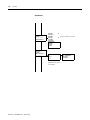
30
30
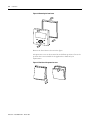
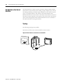
Fitting the Protective Membrane
For special applications such as in the food industry, the keypad must be
protected against the ingress of dust, liquids etc. For this use the specially
designed protective membrane.
Fit the protective membrane before mounting the display/keypad.
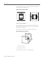
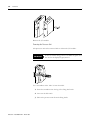
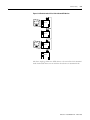
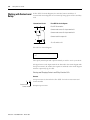
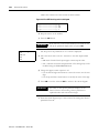
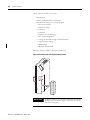
Figure 2.2 Fitting the protective membrane
2
1
1. Protective membrane
2. Display/keypad module
Place the protective membrane over the display/keypad.
Publication 1760-UM002B-EN-P - March 2005
Installation
ATTENTION
2-3
Ensure that the membrane fits snugly in the groove of the
display/keypad.
Otherwise a proper seal cannot be guaranteed and particles
may enter underneath the membrane. This may cause
malfunctions in the keypad.
In food industry applications, there is the risk of bacteria
building up underneath the membrane.
Figure 2.3 Correct position of the protective membrane
IMPORTANT
If the protective membrane needs to be replaced, the
display/keypad must be removed. Replace the membrane
and refit the device.
Mounting the Protective Cover
The protective cover is provided for using the device in aggressive
environments. This protects the display and the keypad against mechanical
damage or destruction. Protection to IP65 is maintained.
The protective cover can be opened so that the keypad can be used.
The protective cover can be closed with a sealing facility to provide protection
against unauthorized operation.
Before mounting the display/keypad, fit the protective cover.
Publication 1760-UM002B-EN-P - March 2005
2-4
Installation
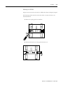
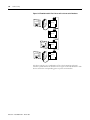
Figure 2.4 Removing the front frame
Remove the front frame as shown in the figure.
The protective cover can be mounted in two different positions. Choose the
position that is most suitable for the application at hand and your
requirements.
Figure 2.5 Position of the protective cover
Publication 1760-UM002B-EN-P - March 2005
Installation
2-5
Figure 2.6 Installing the protective cover
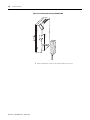
Install the protective cover as shown in the figure.
Sealing the Protective Cover
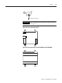
Figure 2.7 Sealing the protective cover
The grip handle of the protective cover is provided with holes that can be used
in any mounting position. You can fit a wire or similar material through these
holes in order to seal the cover. If the wire is provided with a lead seal, the
cover is sealed. The cover can then only be opened by breaking the seal or the
wire.
Publication 1760-UM002B-EN-P - March 2005
2-6
Installation
Mounting the Display/Keypad, “Front Mounting”
Figure 2.8 Drill holes for the GFX
MFD-CP...
22.5
30
Drill and punch out two 22.5 mm diameter holes. The diameter is the same as
is normally required for control circuit devices.
IMPORTANT
Observe the following technical requirements:
• The hole spacing is 30 mm.
• The maximum thickness of the front plate for
mounting the processor unit must not be more than
6 mm.
• The maximum thickness of the front plate for
mounting an expansion unit with a DIN rail in addition
to the processor unit must not be more than 4 mm.
• Leave enough space at the side for the processor unit,
and if necessary, the expansion unit.
• In order to ensure protection to IP65, the surface of the
mounting front must be even and smooth.
Publication 1760-UM002B-EN-P - March 2005
Installation
2-7
Figure 2.9 Mounting the display/keypad
The protective membrane or the protective cover must be fitted.
Fit the display/keypad in the punched fixing holes.
Figure 2.10 Screw fastening the display/keypad
2x
Screw fasten the display/keypad.
Publication 1760-UM002B-EN-P - March 2005
2-8
Installation
IMPORTANT
The tightening torque must be between 1.2 and 2 Nm.
Ensure that the correct torque is used. If the tightening
torque is too low or high, this may impair the seal.
Use the combination box spanner with the designation M22-MS.
Removing the Display/Keypad, “Front Mounting”
Unscrew the fixing element and remove the display/keypad.
Mounting the Processor Unit
If you wish to add expansion units to the processor unit, the DIN rail must be
fitted beforehand.
Fitting the DIN Rail
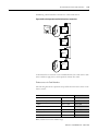
Ensure that the cutout of the DIN rail was prepared for the fixing shafts
according to the specified dimensions.
Figure 2.11 DIN rail with cutout
120
30
216
Publication 1760-UM002B-EN-P - March 2005
38.75
35
23.75
24
60
Installation
IMPORTANT
2-9
The two fixing shafts of the display/keypad are designed
for a 2 space unit expansion device.
If you wish to fit wider expansion units, the DIN rail must
be supported at a third support point.
This third support point should be located in the area
216 mm from the end of the device. It should not be
possible to twist the DIN rail.
ATTENTION
The fixing shafts of the display/keypad are designed for
mounting the expansion units. Other devices such as
contactors must not be mounted on this DIN rail.
Attach the expansion unit before fitting the DIN rail.
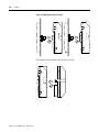
Figure 2.12 Fitting the DIN rail
1. Fit the DIN rail in the groove using the slide catch of the processor unit
and the expansion unit.
2. Turn the DIN rail towards the housing.
3. Let the DIN rail snap into position.
4. Press the processor unit onto the fixing shaft.
Publication 1760-UM002B-EN-P - March 2005
2-10
Installation
Figure 2.13 Mounting the Processor Unit
Mounting the Inputs/Outputs onto the Processor Unit
Publication 1760-UM002B-EN-P - March 2005
Installation
IMPORTANT
2-11
The inputs/outputs can be mounted before or after
mounting the processor unit onto the fixing shaft.
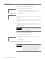
Removing the Inputs/Outputs
1. Press the two catches together.
2. Pull one side out of the catch.
3. Pull the other side out of the second catch.
Publication 1760-UM002B-EN-P - March 2005
2-12
Installation
Remove the I/O module.
Removing the Processor Unit
The processor unit can be removed with or without the I/O module.
IMPORTANT
If there is another fixing point for the DIN rail, apart from
the one for the display/keypad, undo it.
Use a screwdriver with a 100 x 3.5 mm slot width.
1. Insert the screwdriver into the lug of the fixing shaft catch.
2. Lever out the slide catch.
3. Pull out the processor unit from the fixing shafts.
Publication 1760-UM002B-EN-P - March 2005
Installation
2-13
Mounting on a DIN Rail
The processor unit can be mounted on a DIN rail without the display/keypad.
The fastening catches must be removed in order to mount the device on a
fastened DIN rail.
1. Remove the spring with a screwdriver.
2. Pull the slide catch out of the guide and remove it.
Publication 1760-UM002B-EN-P - March 2005
2-14
Installation
3. Hook the Pico GFX-70 to the top edge of the DIN rail and hinge into
place while pressing down slightly.
4. Press down lightly on both the device and the DIN rail until the unit
snaps over the lower edge of the DIN rail. The Pico GFX-70 will clip
into place automatically.
5. Check that the device is seated firmly.
The device is mounted vertically on a DIN rail in the same way.
Screw Mounting
The processor unit can be screwed onto a mounting plate without the
display/keypad.
For screw mounting on a mounting plate, mounting feet must be used that can
be fixed to the back of the Pico GFX-70. The mounting feet are available as an
accessory.
Publication 1760-UM002B-EN-P - March 2005
Installation
CK
CLI
2-15
!
1760-NMF mounting feet
IMPORTANT
Three mounting feet are sufficient for a device with four
fixing points.
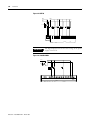
Figure 2.14 Screw mounting for the GFX
Figure 2.15 Screw mounting for the 1760-IA12XOW6I and 1760-IB12XOB8
Publication 1760-UM002B-EN-P - March 2005
2-16
Installation
Connecting the Expansion
Unit
You can only add one Pico expansion I/O module to each controller.
Terminals
Tool for Cage Clamp Terminals
Figure 2.16 Connecting expansion units
Slot-head screwdriver, width 3.5 mm x 0.6 mm.
Connection Cross-Sections of the Cage Clamp Terminal Cables
• Solid: 0.2 to 4 mm2 (AWG 24 -12)
• Flexible with ferrule: 0.2 to 2.5 mm2
(AWG 24-12)
Tool for Slot-Head Screws for Expansion I/O Unit
Slot-head screwdriver, width 3.5 x 0.6 mm, tightening torque 0.6 Nm.
Connection Cross-Sections of Screw Terminal Cables
• Solid: 0.2 to 4 mm2 (AWG 22 - 12)
• Flexible with ferrule: 0.2 to 2.5 mm2
(AWG 22 -12)
Publication 1760-UM002B-EN-P - March 2005
Installation
Connecting the Power
Supply
2-17
The required connection data for both device types GFX,
1760-IB12XOB8 with 24V dc and 1760-IA12XOW6I with
standard voltages of 100V ac to 240V ac are shown on page
A-1.
TIP
The Pico GFX-70 devices run a system test for one second
after the power supply has been switched on. Either RUN
or STOP mode will be activated after this time depending
on the default setting.
1760-IA12XOW6I Expansion Units
Figure 2.17 Power supply on the AC expansion units
L
N
F1
E+ E-
R1
ATTENTION
...
R12 L N N
100-240 V ~
A short current surge will be produced when switching on
for the first time. Do not switch on the module via Reed
contacts since these may burn or melt.
Publication 1760-UM002B-EN-P - March 2005
2-18
Installation
DC Power Supply for the GFX-70
Figure 2.18 Power supply on the GFX
L02+
L01+
L01–
>1A
+24V 0V 0V
The GFX processor unit supplies the necessary power supply to itself, the
display, the input/output electronics, the expansion I/O, and optionally the
Pico-Link cable.
IMPORTANT
Publication 1760-UM002B-EN-P - March 2005
The GFX device processor unit is protected against reverse
polarity. Ensure the correct polarity of the terminals to
ensure that the GFX functions correctly.
Installation
2-19
1760-IB12XOB8 Expansion Module
Figure 2.19 Power supply on the DC expansion units
L01+
L01F1
E+ E-
IMPORTANT
R1
...
R12 24V 0V 0V
24 V
The module is protected against polarity reversal. To ensure
that module works correctly, ensure that the polarity of
each terminal is correct.
Cable Protection
Provide cable protection (F1) for at least 1A (slow).
IMPORTANT
When the expansion I/O or the GFX is switched on for
the first time, its power supply circuit behaves like a
capacitor. Use a suitable device for switching on the power
supply and do not use any Reed relay contacts or proximity
switches.
Publication 1760-UM002B-EN-P - March 2005
2-20
Installation
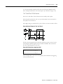
Connecting the Inputs
The inputs switch electronically. Once you have connected a contact via an
input terminal, you can reuse it as a contact in your Pico GFX-70 circuit
diagram as often as you like.
Figure 2.20 Connecting the inputs
L
+24 V
S1
N
0V
I1
I1
i1
Connect contacts such as push button actuators or switches to the input
terminals.
Connecting AC Inputs
ATTENTION
Publication 1760-UM002B-EN-P - March 2005
Connect the inputs to the same line as the power feed in
accordance with the VDE, IEC, UL and CSA safety
regulations. Otherwise the module will not detect the
switching level and may be damaged or destroyed by
overvoltage.
Installation
2-21
Figure 2.21 1760-IA12XOW6I Expansion unit
L1
N
F1
E+ E–
R1 R2 R3 R4
R5
R6
R7 R8 R9
R10 R11 R12
L
N
N
100-240 V
Connect the inputs, for example, to push button actuators, switches or
relay/contactor contacts.
Input signal voltage range
• OFF signal: 0V ac to 40V ac
• ON signal: 79V ac to 264V ac
Input current
• R1 to R12
0.5 mA/0.25 mA at 230V ac/115V ac
Cable Lengths
Severe interference can cause a “1” signal on the inputs without a proper signal
being applied. Observe therefore the following maximum cable lengths:
• R1 to R12: 40m without additional circuit
The following applies to expansion units:
With longer cables, connect a diode (e.g. 1N4007) for 1A, minimum 1 000V
reverse voltage, in series to the input. Ensure that the diode is pointing towards
the input as shown in the circuit diagram, otherwise the module will not detect
the 1 state.
Publication 1760-UM002B-EN-P - March 2005
2-22
Installation
Figure 2.22 1760-IB12XOB8 with a diode on the inputs
L1
N
F1
E+ E–
R1 R2 R3 R4
R5
R6
R7 R8 R9
R10 R11 R12
L
N
N
100-240 V
Two-wire proximity switches have a residual current with the “0” state. If this
residual current is too high, the input may detect a “1” signal.
If inputs with a higher input current are required, an additional input circuit
must be used.
Increasing the Input Current
The following input circuit can be used in order to prevent interference and
also when using two-wire proximity switches:
Figure 2.23 Increasing the input current
L1
N
F1
100 nF/275 V h
E+ E–
R1 R2 R3 R4
R5
R6
100-240 V
Publication 1760-UM002B-EN-P - March 2005
R7 R8 R9
R10 R11 R12
L
N
N
Installation
IMPORTANT
2-23
When using a 100 nF capacitor, the drop-out time of the
input increases by 80 (66.6) ms at 50 (60) Hz.
A resistor can be connected in series with the circuit shown in order to restrict
the inrush current.
Figure 2.24 Limitation of the inrush current with a resistor
L1
N
F1
1 kO
100 nF/275 V h
E+ E–
R1 R2 R3 R4
R5
R6
R7 R8 R9
R10 R11 R12
L
N
N
100-240V
Connecting DC Inputs
Use input terminals I1 to I12 to connect push button actuators, switches or 3
or 4-wire proximity switches. Given the high residual current, do not use
2-wire proximity switches.
Input signal voltage range
• I1 to I6, I9, I10
– OFF signal: 0V dc to 5V dc
– ON signal: 15V dc to 28.8V dc
• I7, I8, I11, I12
– OFF signal: < 8V dc
– ON signal: > 8V dc
Input current
• I1 to I6, I9, I10, R1 to R12: 3.3 mA at 24V dc
• I7, I8, I11, I12: 2.2 mA at 24V dc
Publication 1760-UM002B-EN-P - March 2005
2-24
Installation
Figure 2.25 GFX DC
L01+
L02+
L01–
>1A
+24V 0V 0V
IMPORTANT
I1 I2 I3 I4 I5 I6 I7 I8 I9 I10 I11 I12
The digital inputs must have the same voltage as the power
supply of the GFX.
Figure 2.26 1760-IB12XOB8
L01 +
L01 –
F1
E+ E–
R1 R2 R3 R4
R5
R6
24 V H
Publication 1760-UM002B-EN-P - March 2005
R7 R8 R9
R10 R11 R12 +24V 0V
0V
Installation
2-25
Connecting Analog Inputs
Inputs I7, I8, I11 and I12 can also be used to connect analog voltages ranging
from 0V dc to 10V dc.
The following applies:
•
•
•
•
I7 = IA01
I8 = IA02
I11 = IA03
I12 = IA04
The resolution is 10-bit = 0 to 1023.
ATTENTION
Analog signals are more sensitive to interference than
digital signals. Consequently, more care must be taken
when laying and connecting the signal lines. Incorrect
switching states may occur if they are not connected
correctly.
• Use shielded twisted pair cables to prevent interference with the analog
signals.
• For short cable lengths, ground the shield at both ends using a large
contact area. If the cable length exceeds 30m or so, grounding at both
ends can result in equalization currents between the two grounding
points and thus in the interference of analog signals. In this case, only
ground the cable at one end.
• Do not lay signal lines parallel to power cables.
• Connect inductive loads to be switched via the Pico GFX-70 outputs to
a separate power feed, or use a suppressor circuit for motors and valves.
If loads such as motors, solenoid valves or contactors are operated with
Pico GFX-70 via the same power feed, switching may give rise to
interference on the analog input signals.
The following circuits contain examples of applications for analog value
processing.
IMPORTANT
Ensure that the reference potential is connected. Connect
the 0V of the power supply unit for the different set point
potentiometers and sensors shown in the examples to the
0V terminal of the Pico GFX-70 power feed.
Publication 1760-UM002B-EN-P - March 2005
2-26
Installation
Set Point Potentiometer
Figure 2.27 Set Point potentiometer, set point potentiometer with upstream resistor
L01+
L02+
L01–
>1A
1.3 kO/0.25 W
1 kO/0.25 W
h
H
0V
+24V 0V 0V
I1
I2
I3
I4 I5
I6 I7
+12 V
I8 I9 I10 I11 I12
Use a potentiometer with a resistance of greater than or equal to1 kΩ, e.g. 1 kΩ,
0.25W.
Temperature Sensor, Brightness Sensor, 20 mA Sensor
Figure 2.28 Temperature sensor, brightness sensor, 20 mA sensor
L02+
L01+
L01–
h
H
>1A
0V
+12 V
+24 V H
0...10 V
a
–35...55 ˚C
4...20 mA
0V
Out
0...10 V
500 O
+24V 0V 0V
I1
I2
I3
I4 I5
I6 I7
I8 I9 I10 I11 I12
4 to 20 mA (0 to 20 mA) sensors can be connected using an external 500 Ω
resistor.
The following values apply:
• 4 mA = 1.9V
• 10 mA = 4.8V
• 20 mA = 9.5V
(according to U = R x I = 478 Ω x 10 mA ~ 4.8V)
Publication 1760-UM002B-EN-P - March 2005
Installation
2-27
Connecting High-Speed Counters and Frequency Generators
High-speed counter signals on the Pico GFX-70 can be counted correctly on
inputs I1 to I4 independently of the cycle time.
Figure 2.29 High-speed counter, frequency generator
L02+
L01+
L01–
>1A
+24V 0V 0V
I1
I2
I3
I4 I5
I6 I7
I8 I9 I10 I11 I12
Connecting Incremental Encoders
Inputs I1, I2 and I3, I4 on the Pico GFX-70 can each be used for the
high-speed counting of an incremental encoder independently of the cycle
time. The incremental encoder must generate two 24V dc square wave signals
with a 90° phase shift between them.
Figure 2.30 Connecting incremental encoders
L01+
L02+
L01–
>1A
A
+24V 0V 0V
B
I1 I2 I3 I4 I5 I6 I7 I8 I9 I10 I11 I12
Publication 1760-UM002B-EN-P - March 2005
2-28
Installation
Connecting the Outputs
The Q... outputs function inside the Pico GFX-70 as isolated contacts.
Figure 2.31 Output “Q”
Q1
1
2
The respective relay coils are actuated in the Pico GFX-70 circuit diagram via
the output relays Q 01 to Q 04 or S 01 to S 06 (S 08). You can use the signal
states of the output relays as make or break contacts in the Pico GFX-70
circuit diagram for additional switching conditions.
The relay or transistor outputs are used to switch loads such as fluorescent
tubes, filament bulbs, contactors, relays or motors. Check the technical
thresholds and output data before installing such devices. (See page A-1.)
Connecting Relay Outputs
1760-IB12XOW4IF, 1760-IB12XOW4IOF
Figure 2.32 1760-IB12XOW4IF, 1760-IB12XOW4IOF relay outputs
R
1
f 10 000 000
Q1
1
2
Q2
2
1
2
Q3
1
2
24 V H 8 A
115 V h 8 A
230 V h 8 A
1000 W
Q4
10 x 58 W
M
0 V H, N
f 8 A/B 16
L1, L2, L3 (115/250 V h)
+24 V H
Publication 1760-UM002B-EN-P - March 2005
...
...
2A
2A
2A
...
25 000
Installation
2-29
1760-IA12XOW6I
Figure 2.33 1760-IA12XOW6I relay outputs
1 2
S1
1 2
S2
1 2
S3
1 2
1 2
S4
S5
1 2
R
S6
24 V H 8 A
115 V h 8 A
230 V h 8 A
10 000 000
2A
2A
2A
1000 W
0 V H, N
10 x 58 W
25 000
F 8 A/B 16
L1, L2, L3 (115/230 V h)
+ 24 V H
1760-OW2
Figure 2.34 1760-OW2 relay outputs
1
S1
10 000 000
2
1 2
R
S2
24 V H 8 A
115 V h 8 A
230 V h 8 A
2A
2A
2A
1000 W
0 V H, N
10 x 58 W
25 000
F 8 A/B 16
L1, L2, L3 (115/230 Vh)
+ 24 V H
Unlike the inputs, the 1760-IB12XOW4IF, 1760-IB12XOW4IOF, and
1760-IA12XOW6I, relay outputs can be connected to different lines.
ATTENTION
Do not exceed the maximum voltage of 250V ac on a relay
contact. If the voltage exceeds this threshold, flashover
may occur at the contact, resulting in damage to the device
or a connected load.
Publication 1760-UM002B-EN-P - March 2005
2-30
Installation
Connecting Transistor
Outputs
1760-IB12XOB4IF, 1760-IB12XOB4IOF
Figure 2.35 1760-IB12XOB4IF, 1760-IB12XOB4IOF transistor outputs
R
+ 24 V H
(20.4 – 28.8 V H)
24 V H
0.5 A
0.5 A
5 W/24 V
F 10 A
24 VQ
0 VQ
Q1
Q2
Q3
Q4
1760-IB12XOB8
Figure 2.36 1760-IB12XOB8 transistor outputs
24 VQ
S1
S2
S3
S4
S5
S6
S7
0 VQ
S8
F 10 A
0VH
f 2.5 A
R
+ 24 V H
(20.4 – 28.8 V H)
24 V H
0.5 A
0.5 A
5 W/24 V
Parallel connection:
Up to four outputs can be connected in parallel in order to increase the power.
The output current will increase in this case to a maximum of 2 A.
Publication 1760-UM002B-EN-P - March 2005
Installation
ATTENTION
ATTENTION
2-31
Outputs may only be connected in parallel within a group
(Q1 to Q4 or Q5 to Q8, S1 to S4 or S5 to S8), such as Q1
and Q3 or Q5, Q7 and Q8. Outputs connected in parallel
must be switched at the same time.
Please note the following when switching off inductive
loads:
Suppressed inductive loads cause less interference in the
entire electrical system. For optimum suppression the
suppressor circuits are best connected directly in the
proximity of the inductive load.
If inductive loads are not suppressed, the following applies:
Several inductive loads should not be switched off simultaneously to avoid
overheating the driver blocks in the worst possible case. If in the event of an
emergency stop the +24V dc power supply is to be switched off by means of a
contact, and if this would mean switching off more than one controlled output
with an inductive load, then you must provide suppressor circuits for these
loads (see the following diagrams).
Figure 2.37 Inductivity with suppressor circuit
+ 24 V H
Uemax < UZ < 33 V
Q., S.
Q., S.
0VH
Short-Circuit and Overload Behavior
Should a short circuit or overload occur on a transistor output, this output will
switch off. The output will switch on up to maximum temperature after the
cooling time has elapsed. This time depends on the ambient temperature and
the current involved. If the fault condition persists, the output will keep
switching off and on until the fault is corrected or until the power supply is
switched off. (See Monitoring of Short-Circuit and Overload with 1760-IB12XOB8
on page 8-7).
Publication 1760-UM002B-EN-P - March 2005
2-32
Installation
Connecting Analog Outputs
1760-IB12XOW4IOF and 1760-IB12XOB4IOF each have an analog output
QA 01, 0V dc to 10V dc, 10 bit resolution (0 to 1023). The analog output
allows you to control servo valves and other final controlling elements.
ATTENTION
Analog signals are more sensitive to interference than
digital signals. Consequently, more care must be taken
when laying and connecting the signal lines. Incorrect
switching states may occur if they are not connected
correctly.
Connecting Servo Valves
Figure 2.38 Connecting servo valves
L01+
L02+
L01–
>1A
A
+24V 0V 0V
Publication 1760-UM002B-EN-P - March 2005
I1
I2
B
I3
I4 I5
I6 I7
I8 I9 I10 I11 I12 0V 0V QA 1
Installation
2-33
Setpoint Entry for a Drive
Figure 2.39 Setpoint entry for a drive
L02+
L01+
L01–
>1A
0V IA
A
+24V 0V 0V
Connecting the Pico-Link
I1
I2
B
I3
I4 I5
I6 I7
I8 I9 I10 I11 I12 0V 0V QA 1
Pico GFX-70 with network connection (1760-LDFC) can be used for creating
the Pico-Link network. Up to eight devices can be connected to this network.
Further information can be found in Pico-Link and Point-to-Point Serial
Connections on page 6-1.
Accessories
Connection Plug
8-pole RJ45, 1760-CONN-RJ45
Connection Assignment of the RJ45 Socket on the Device
Figure 2.40 RJ45 socket
1
2
3
4
5
6
7
8
Publication 1760-UM002B-EN-P - March 2005
2-34
Installation
Connection Cable
4-pair twisted cable; see General on page A-1
Figure 2.41 Connection assignment
A
A
B
B
1
2
3
4
ECAN_H
ECAN_L
GND (Ground)
SEL_IN
ECAN_H data cable, pin 1, cable pair A
ECAN_L data cable, pin 2, cable pair A
Ground cable GND, pin 3, cable pair B
Select cable SEL_IN, pin 4, cable pair B
IMPORTANT
Minimum operation with Pico-Link functions with the
cables ECAN_H, ECAN_L and GND. The SEL_IN cable
is only used for automatic addressing.
Table 2.42 Prefabricated Cables (RJ45 plug on both ends)
Catalog Number
Cable Length (cm)
1760-CBL-INT01
30
1760-CBL-INT03
80
1760-CBL-INT05
150
Material for Self-Manufactured Cables
• 100m cable: 1760-CBL-INT300
• Crimping tool for RJ45 plug
Bus Termination Resistor
The first and last stations in the network must be provided with a bus
termination resistor.
• Value: 124 Ω
• Termination connector: 1760-TERM1
Publication 1760-UM002B-EN-P - March 2005
Installation
2-35
Cable Length and Cross-Sections
For correct operation of the network, the cable lengths, cross-sections and
cable resistances must correspond to the following table.
Table 2.43
Cable length
Cable Resistance
Cross-section
m
mΩ/m
mm2
AWG
up to 40
≤ 140
0.13
26
up to 175
≤ 70
0.25 to 0.34
23, 22
up to 250
≤ 60
0.34 to 0.5
22, 21, 20
up to 400
≤ 40
0.5 to 0.6
20, 19
up to 600
≤ 26
0.75 to 0.8
18
up to 1000
≤ 16
1.5
16
The surge impedance of the cables used must be 120 Ω.
Calculating the Cable Length with Known Cable Resistance
If the resistance of the cable per unit of length is known (resistance per unit
length R’ in Ω/m), the entire cable resistance RL must not exceed the following
values. RL depends on the selected baud rates:
Baud rate
Cable resistance RL
kBaud
Ω
10 to 125
≤ 30
250
≤ 25
500
≤ 12
1000
lmax = maximum cable length in m
RL = Total cable resistance in Ω
R’ = Cable resistance per unit length in Ω/m
lmax = RL
R’
Publication 1760-UM002B-EN-P - March 2005
2-36
Installation
Calculating Cross-Section with Known Cable Lengths
The minimum cross-section is determined for the known maximum extent of
the network.
l = cable length in m
Smin = minimum cable cross-section in mm2
ρ cu = resistivity of copper, if not otherwise stated 0.018 Ω mm2/m
Smin = l x ρ cu
12.4
IMPORTANT
If the result of the calculation does not yield a standard
cross-section, the next larger cross-section is used.
Calculating Length with Known Cable Cross-Section
The maximum cable lengths are calculated for a known conductor
cross-section.
lmax = cable length in m
S = minimum cable cross-section in mm2
ρ cu = resistivity of copper, if not otherwise stated 0.018 Ω mm2/m
lmax = S x 12.4
ρ cu
Plugging and Unplugging Network Cables
Pico GFX-70 is provided with two RJ45 network sockets.
The socket 1 in the first station is for the bus terminating resistor. For other
stations, socket 1 is used for plugging in the incoming cable. Socket 2 is used
for the outgoing cable or for the bus termination resistor on the last physical
station in the network.
Publication 1760-UM002B-EN-P - March 2005
Installation
2-37
Figure 2.44 Bus termination resistors
Terminating
Resistor
Location 1
First Station on the Pico-Link
Station 1
R 1 - 12
GFX-70
S1-8
Location 2
GFX-70
GFX-70
Station 2
Location 3
GFX-70
Station 3
Location 8
Last Station on the Pico-Link
Station 8
GFX-70
Terminating
Resistor
Both RJ45 interfaces are visible after the cover plate has been removed.
When a cable is plugged in, the mechanical connection must be audible (click)
and visible.
Before a plug or cable is removed, the mechanical locking feature must be
undone.
Figure 2.45 Plugging and unplugging cables
1
2
3
Publication 1760-UM002B-EN-P - March 2005
2-38
Installation
Connecting the Serial
Interface
The GFX processor unit is provided with a multi-function interface. This can
be used to set up point-to-point communication between different devices.
The interface is also used for connecting PicoSoft Pro.
The serial interface must be implemented using special cables.
The standard 1760-CBL-2M cable is 2m in length.
IMPORTANT
The 1760-CBL-2M cable must not be lengthened in order
ensure compliance with EMC requirements.
1. Remove the interface cover or other plugs from the interface.
2. Fit the connectors in the devices.
Publication 1760-UM002B-EN-P - March 2005
Installation
2-39
a
IMPORTANT
It must be ensured in all circumstances that the connector
with the marking POW-Side is fitted in the interface of the
GFX device. The serial interface only functions if the GFX
device is providing the power feed required for the
interface cable.
Figure 2.46 Point-to-point serial interface
POW-Side
Publication 1760-UM002B-EN-P - March 2005
2-40
Installation
Expanding Inputs/Outputs
You can add expansion units to all GFX types with an expansion I/O socket
to increase the number of inputs and outputs:
Table 2.47 Pico Expansion I/O Modules
Processor Unit
I/O Modules
Description
1760-LDF
1760-LDFA
1760-LDFC
1760-LDFCA
1760-IA12XOW6I
12 AC inputs, 6 relay outputs
1760-IB12XOB8
12(1) DC inputs, 8 transistor outputs
1760-IB12XOW6I
12 DC inputs, 6 isolated relay outputs
1760-OW2
2 relay outputs
(1) Four of the digital dc inputs can alternately be used as 0 to 10V dc analog inputs. These inputs can be used as
either digital or analog, not both. For example you could use 4 analog inputs plus 8 digital inputs.
Local Expansion
Local expansion units are fitted directly next to the processor unit with the
expansion I/O socket connection.
Figure 2.48 Connecting local expansion units with Pico GFX-70 processors
1760-RPLCONN
processor unit
ATTENTION
expansion I/O
The following electrical separation is implemented between
the processor unit of the GFX device and the expansion
unit (separation always in local connection of expansion
unit)
• Simple isolation 400V ac (+10%)
• Safe isolation 240V ac (+10%)
Units may be destroyed if the value 400V ac +10% is
exceeded, and may cause the malfunction of the entire
system or machine.
IMPORTANT
Publication 1760-UM002B-EN-P - March 2005
GFX processor units and expansion units can be fed by
different DC power supplies.
Installation
2-41
Remote Expansion
Expansion I/O modules can be located remotely from the primary controller
by using the Pico-Link or serial interface. See Configuring a Pico-Link Network on
page 3-14 and Configuring the Connection for the Terminal Mode on page 3-20 for
more information.
Installing the Remote
Processor
The remote processor is used for terminal mode operation of Pico controllers
and I/O modules. The remote processor is used with either a Display or
Display/Keypad Unit.
Figure 2.49 Remote Processor Terminal Operation
1760-LDF...
1760-RM-GFX
Mounting and Removal
Flush Mounting
Figure 2.50 Flush Mounting Display and Remote Processor
3
2
1
M = 1.2 – 2 Nm
10.6 - 17.7 lb-in
2
1. Insert the display unit through the mounting holes on the panel.
Publication 1760-UM002B-EN-P - March 2005
2-42
Installation
2. Attach the fixing rings.
3. Attach the processor unit.
Removal Procedure
Figure 2.51 Removing the Remote Processor
3
2
1
1760 -RM
1. Insert the screwdriver into the mounting slide.
2. Push screwdriver to the right to open the slide.
3. Remove the processor unit from the display unit.
4. Loosen the fixing rings.
5. Remove the display unit from the panel.
Making Connections
Connecting the Power Supply
Figure 2.52 Remote Processor Power Supply Connection
1760-RM…
L01+
L02+
L01–
>1 A
U e = 24 V dc
(20.4 – 28.8 V H dc)
I e = 150 mA
0.6 x 3.5 x 100
24V 0V
Publication 1760-UM002B-EN-P - March 2005
Installation
2-43
Connecting the Serial Cable
4
2
1
3
Cable Wire Color Code
1760- RM... cable
X5
X4
X3
X2
X1
X5
X4
X3
X2
X1
green
white
yellow
brown
gray
1. Remove the interface cover.
2. Using a screwdriver, push on the terminal latch.
3. Insert each wire into its designated terminal on the interface connector.
4. Replace the interface cover.
Plug the other end of the cable into the Pico controller or I/O module.
Publication 1760-UM002B-EN-P - March 2005
2-44
Installation
Publication 1760-UM002B-EN-P - March 2005
Chapter
3
Commissioning
Before startup check whether the power supply, inputs, outputs, the
serial interface and the Pico-Link cable are properly connected:
Switching On
• 24V dc version:
– Terminal +24V: +24V voltage
– Terminal 0V: 0V voltage
– Terminals I1 to I12, R1 to R12:
Actuation via +24V
• 230V ac version
– Terminal L: Phase conductor L
– Terminal N: Neutral conductor N
– Terminals R1 to R12:
Actuation via phase conductor L
If you have already integrated devices into a system, secure any parts
of the system connected to the working area to prevent access and
ensure that no-one can be injured if, for example, motors start up
unexpectedly.
Setting the Menu Language
ENGLISH
✓
When you switch on the Pico GFX-70 for the first time, you will be asked to
select the menu language.
1. Use the up and down arrow buttons to select the language
required.
DEUTSCH
FRANCAIS
ESPANOL
1
–
–
–
–
–
–
–
–
–
–
English
German
French
Spanish
Italian
Portuguese
Dutch
Swedish
Polish
Turkish
Publication 1760-UM002B-EN-P - March 2005
3-2
Commissioning
2. Press OK to confirm your choice and press ESC to exit the menu. GFX
will then switch to the Status display.
IMPORTANT
You can change the language setting at a later date, if
you wish. See Changing the Menu Language on page 7-8.
If you do not set the language, the Pico GFX-70 will display
this menu every time you switch on and wait for you to
select a language.
Operating Modes
Pico GFX-70 operating modes - RUN, STOP and TERMINAL MODE.
In RUN mode the GFX continuously processes a stored program until you
select STOP, disconnect the power supply or switch to TERMINAL MODE.
The program, parameters and the GFX settings are retained in the event of a
power failure. All you will have to do is reset the real-time clock after the
back-up time has elapsed. Circuit diagram entry is only possible in STOP
mode.
IMPORTANT
In RUN mode, the processor will immediately run the
program saved in the unit when the power supply is
switched on. This will not happen if STOP or TERMINAL
mode was set as startup mode. In RUN mode, outputs are
activated according to the switch logic involved.
The following applies to devices without display/keypad:
• Memory module containing a valid circuit diagram must be fitted.
• Device must be switched on.
If the device has no program, the program stored on the memory module is
loaded automatically and the device immediately starts running the program in
RUN mode.
Publication 1760-UM002B-EN-P - March 2005
Commissioning
Creating your First Circuit
Diagram
3-3
The following single line diagram takes you step by step through wiring up
your first circuit diagram. In this way you will learn all the rules, quickly
enabling you to use Pico GFX-70 for your own projects.
As with conventional wiring, you use contacts and relays in the Pico GFX-70
diagram. With Pico GFX-70, however, you no longer have to connect up
components individually. At the push of a few buttons, the Pico GFX-70
circuit diagram produces all the wiring required. All you have to do is then
connect any switches, sensors, lamps or contactors you wish to use.
Figure 3.1 Lamp controller with relays
L01+
F1
S1
K1
S2
K1
H1
L01-
Publication 1760-UM002B-EN-P - March 2005
3-4
Commissioning
In the following example, Pico GFX-70 carries out all the wiring and performs
the tasks of the circuit diagram shown below.
Figure 3.2 Lamp controller with GFX
L01+
L01–
F1
S1
+24V 0V 0V
S2
I1 I2 I3
I 01----I 02-
--Ä Q 01
ALT
DEL
OK
ESC
1
H1
L01–
Publication 1760-UM002B-EN-P - March 2005
Q1
2
*
Commissioning
3-5
Starting Point Status Display
I ............
I
P-
MO 02:00
Q........
When you switch on Pico GFX-70, it opens the Status display immediately to
show the switching state of the inputs and outputs. It also indicates whether
the processor is already running a program. Note: If another display is visible,
a visualization screen is shown.
STOP
The examples were written without the use of
expansion units. If an expansion unit is connected,
the Status display will first show the status of the
basic unit and then the status of the expansion unit
before showing the first selection menu.
TIP
In this case Pico GFX-70 must be in STOP mode.
1. Press OK to switch to the main menu.
PROGRAM...
STOP ✓
RUN
PARAMETERS
2. Press OK to switch to the next menu level, and press ESC to move one
level back.
SET CLOCK...
TIP
OK has two other functions:
• Press OK to save modified settings.
• In the circuit diagram, you can also press OK to
insert and modify contacts and relay coils.
CIRCUIT DIAGRAM
FUNCTION RELAYS
3. Press OK twice to enter the circuit diagram display via menu items
PROGRAM… −−> PROGRAM. This is where you will create the circuit
diagram.
Publication 1760-UM002B-EN-P - March 2005
3-6
Commissioning
Circuit Diagram Display
❚
The circuit diagram display is currently empty. The cursor flashes at the top
left, which is where you will start to create your diagram.
The location of the cursor is indicated in the status line. L: = Circuit
connection (line), C: = Contact or coil (contact), B: = Free memory available
in bytes. Start value 7944, with the first three circuit connections already
generated.
The Pico GFX-70 circuit diagram supports 4 contacts and one coil in series.
The Pico GFX-70 display can display 6 circuit diagram contact fields.
❚❚❚❚❚❚❚M-❚❚❚❚❚❚❚m -❚❚❚❚❚❚❚
l
❚❚❚❚❚❚❚
L
❚❚❚❚❚❚❚-❚❚❚❚❚❚❚L: 1 C:1 B:7944
Use the up, down, left and right arrow buttons to move the cursor over the
invisible circuit diagram grid.
The first four columns are contact fields, the fifth column is a coil field. Each
line is a circuit connection. Pico GFX-70 automatically connects the contact to
the power supply.
Figure 3.3 Circuit diagram with inputs I1, I2 and output Q1
I 01----I 02--...-[ Q 01
L: 1 C:1 B:7944
Now try to wire up the following Pico GFX-70 diagram.
Switches S1 and S2 are at the input. I 01 and I 02 are the contacts for the input
terminals. Relay K1 is represented by the relay coil [ Q 01. The symbol [
identifies the coil's function, in this case a relay coil acting as a contactor. Q 01
is one of the Pico GFX-70 output relays.
Publication 1760-UM002B-EN-P - March 2005
Commissioning
3-7
From the First Contact to the Output Coil
With Pico GFX-70, you work from the input to the output. The first input
contact is I 01.
1. Press OK.
I 01
Pico GFX-70 proposes the first contact I
L: 1 C:1 B:7944
I 01
01
at the cursor position.
I flashes and can be changed, for example, to a P for a push button
input using the up/down arrows keys. However, nothing needs to be
changed at this point.
2. Press OK twice, to move the cursor across the 01 to the second contact
field.
❚
L: 1 C:1 B:7944
You could also move the cursor to the next contact field using the left
arrow button.
3. Press OK.
I 01
I 02
L: 1 C:2 B:7944
Again, Pico GFX-70 inserts a contact I 01 at the cursor position.
Change the contact number to I 02, so that break contact S2 can be
connected to input terminal I2.
4. Press OK so that the cursor jumps to the next position and use the
up/down arrow keys to change the number to 02.
TIP
You can press DEL to delete a contact at the
cursor position.
5. Press OK to move the cursor to the third contact field.
-I 02
Â
You do not need a third relay contact, so you can now wire the contacts
directly up to the coil field.
L: 1 C:3 B:7944
Publication 1760-UM002B-EN-P - March 2005
3-8
Commissioning
Wiring
Pico GFX-70 displays a small arrow l in the circuit diagram when creating the
wiring.
1. Press ALT to activate the wiring arrow cursor and use the arrow buttons
to move it.
TIP
ALT also has two other functions depending
on the cursor position:
• In the left contact field, you can press ALT
to insert a new empty circuit connection.
• The contact under the cursor can be
changed between a make and break contact
by pressing the ALT button.
❚❚❚❚❚❚❚
M-❚❚❚❚❚❚❚❚❚❚❚ml❚❚-l❚❚❚❚❚❚❚L -❚❚❚❚❚❚❚❚❚❚❚❚❚❚
The wiring arrow works between contacts and relays. When you move
the arrow onto a contact or relay coil, it changes back to the cursor and
can be reactivated with ALT if required.
L: 1 C:1 B:7944
TIP
-I 02
l
Pico GFX-70 automatically wires adjacent contacts
in a circuit connection up to the coil.
2. Press ALT to wire the cursor from I 02 through to the coil field.
The cursor changes into a flashing wiring arrow and automatically
jumps to the next possible wiring position.
3. Press the left arrow button. Contact I 02 will be connected up to the coil
field.
TIP
You can use DEL to erase a connection at the
cursor or arrow position. Where connections
intersect, the vertical connections are deleted
first, then, if you press DEL again, the
horizontal connections are deleted.
4. Press the left arrow button again.
The cursor will move to the coil field.
5. Press OK.
--------[ Q 01
Pico GFX-70 inserts the relay coil Q 01. The specified coil function [
and the output relay Q 01 are correct and do not have to be changed.
L: 1 C:1 B:7944
Your first working Pico GFX-70 circuit diagram now looks like this:
Publication 1760-UM002B-EN-P - March 2005
Commissioning
3-9
Figure 3.4 Your first circuit diagram
I 01----I 02-------------------[ Q 01
L: 1 C:1 B:7944
= visible area
6. Press ESC to leave the circuit diagram display.
The SAVE menu appears.
Figure 3.5 SAVE menu
I 01----I 02-------------------[ Q 01
SAVE
Ó
= visible area
7. Press the OK button.
The circuit diagram is stored.
Once you have connected push button actuators S1 and S2, you can test
your circuit diagram.
Publication 1760-UM002B-EN-P - March 2005
3-10
Commissioning
Testing the Circuit Diagram
1. Switch to the main menu and select the STOP RUN menu option.
PROGRAM...
STOP ✓ RUN
With a tick at RUN or STOP you switch to the RUN or STOP operating
modes.
PARAMETERS
SET CLOCK...
Pico GFX-70 runs in the mode indicated by the tick.
2. Press the OK button. Pico GFX-70 will change to RUN mode.
The mode assigned the tick is always active.
TIP
The Status display shows the current mode and the switching states of
the inputs and outputs.
3. Change to the Status display and press push button actuator S1.
I 12..........
I
P-
MO 14:42
Q 1.......
RUN
The contacts (boxes) for inputs I1 and I2 are activated and relay Q1
picks up. This is indicated on the numbers which are displayed.
Power Flow Display
The Pico GFX-70 allows you to check circuit connections in RUN mode. This
means that you can check your circuit diagram via the built-in power flow
display while it is being processed by the Pico GFX-70.
1. Change to the Circuit diagram display and press push button actuator
S1.
The relay picks up. Pico GFX-70 shows the power flow.
Figure 3.6 Power flow display: Inputs I1 and I2 are closed, relay Q1 has picked up
I 01====I 02===================[ Q 01
L: 1 C:1 RUN
= visible area
2. Press push button actuator S2, that has been connected as a break
contact.
The circuit connection is interrupted and relay Q1 drops out.
Publication 1760-UM002B-EN-P - March 2005
Commissioning
3-11
Figure 3.7 Power flow display: Input I1 is closed, input I2 is open, relay Q1 has
picked up
I 01====I 02-------------------[ Q 01
L: 1 C:1 RUN
= visible area
3. Press ESC to return to the Status display.
TIP
With Pico GFX-70 you can test parts of a circuit
diagram before it is entirely completed.
Pico GFX-70 simply ignores any incomplete wiring
that is not yet working and only runs the finished
wiring.
Power Flow Display with Zoom Function
The Pico GFX-70 enables you to check the following at a glance:
• all four contacts plus one coil in series
• and 3 circuit connections
Change to the Circuit diagram display and press the ALT button. Press push
button actuator S1.
Figure 3.8 Power flow display in Zoom function: Input I1 and I2 are closed, relay Q1
picked up
❚==❚========[❚
L: 001
I 01
❚ Contact closed, coil is triggered
Contact opened, coil dropped out
1. Press push button actuator S2, that has been connected as a break
contact.
The circuit connection is interrupted and relay Q1 drops out.
❚==#--------[#
L: 001
I 01
Publication 1760-UM002B-EN-P - March 2005
3-12
Commissioning
Use the arrow keys to move between the contacts or coil.
2. Press the up cursor button.
❚==#--------[#
L: 002
I 02
The cursor moves to the second contact.
3. Press the ALT button. The display changes to display status with contact
and/or coil designation.
Figure 3.9 Power flow display: Input I1 is closed, input I2 is open, relay Q1 has
dropped out
I 01====I 02-------------------[ Q 01
L: 1 C:2 RUN
= visible area
Publication 1760-UM002B-EN-P - March 2005
Commissioning
3-13
Deleting the Circuit Diagram
1. Switch the Pico GFX-70 to STOP mode.
IMPORTANT
Pico GFX-70 must be in STOP mode in order to extend,
delete or modify the circuit diagram.
2. Use PROGRAM… to switch from the main menu to the next menu
level.
3. Select DELETE PROGRAM
PROGRAM...
DELETE PROGRAM
The Pico GFX-70 will display the prompt DELETE?
4. Press OK to delete the program or ESC to cancel.
5. Press ESC to return to the Status display.
Fast Circuit Diagram Entry
You can create a circuit diagram in several ways: The first option is to enter the
elements in the circuit and then to wire all the elements together. The other
option is to use the enhanced operator guidance of Pico GFX-70 and create
the circuit diagram in one go, from the first contact through to the last coil.
If you use the first option, you will have to select some of the elements in
order to create and connect up your circuit diagram.
The second, faster option is what you learned in the example. In this case you
create the entire circuit connection from left to right.
Publication 1760-UM002B-EN-P - March 2005
3-14
Commissioning
Configuring a Pico-Link
Network
If you want to work with the Pico-Link network and communicate with several
stations, the network must be configured first.
Proceed as follows:
1. Connect all network stations. Pico-Link socket 2e to Pico-Link socket
1L.
2. The first station 1 (socket 1L) and the last station (socket 2e) must be
provided with a network termination resistor a.
3. Connect all stations to the power supply.
Figure 3.10 Example topology with two Pico-Link stations
1
Resistor
Location 1
Station 1
1
Terminating
R1 – 12
Location 2
Station 2
Resistor
GFX-70
S1 – S8
1. Switch on the power supply on all stations.
2. Ensure that all stations have a power supply. The POW LED must light
up or flash. It is only possible to configure the stations which are
supplied with voltage.
Publication 1760-UM002B-EN-P - March 2005
Commissioning
3-15
3. Proceed to the first physical station (Location 1). This station has the
termination resistor inserted on socket 1.
IMPORTANT
The following tasks are only possible in STOP mode.
Entering the Network Station Number
1. Simultaneously press the DEL and ALT buttons while the GFX displays
the Status display.
SECURITY...
SYSTEM...
MENU LANGUAGE
CONFIGURATOR...
NET..
COM...
LINK....
NET PARAMETERS...
STATIONS...
CONFIGURE
NET-ID : 00
▲
BAUDRATE: 125KB
BUSDELAY: 00
SEND IO
✓ ▼
REMOTE RUN
REMOTE IO
NET-ID : 01
▲
BAUDRATE: 125KB
BUSDELAY: 00
SEND IO
✓ ▼
REMOTE RUN
REMOTE IO
The System menu appears
2. Select the CONFIGURATOR menu option.
3. Press the OK button.
The NET menu appears.
4. Press the OK button.
The NET PARAMETERS… menu appears.
5. Press the OK button.
6. Press the OK button and select the station number using the up/down
arrows keys. In this case the station number (Pico-Link ID) “01”.
7. Press the OK button.
8. Exit the NET PARAMETERS menu with ESC.
IMPORTANT
The station designated station number 1 is the active
station. For this reason the REMOTE RUN and
REMOTE IO functions are not available.
Publication 1760-UM002B-EN-P - March 2005
3-16
Commissioning
Entering Network Stations
Only the network station at physical location 1 with station number 1 has a
station list.
IMPORTANT
The left-hand column is the physical location. You
can only assign a physical location to unused station
numbers. Physical location 1 is permanently assigned
to station number 1.
1. Use the up/down arrow keys to select the STATION menu and press
the OK button.
1
2
3
4
1
0
0
0
▲
1
2
3
4
1
2
0
0
▲
▼
▼
2. Proceed to the station with physical address 2.
3. Select the required physical location with the up/down arrow keys. Press
the OK button.
4. Use up/down arrow keys to select station number 2.
5. Press the OK button.
At physical location 2, the station has been assigned station address 2.
6. Press ESC to return to the STATIONS menu item.
Publication 1760-UM002B-EN-P - March 2005
Commissioning
3-17
Configuring a Pico-Link Network
The Pico-Link network can only be configured from station 1.
Requirement:
All stations are correctly connected to the network and the termination
resistors have been connected.
All stations have a power supply and are in STOP mode. The POW LED is
permanently lit. The NET LED is permanently lit.
IMPORTANT
NET PARAMETERS..
STATIONS...
CONFIGURE
CONFIGURE?
CONFIGURATION
IN
PROGRESS.
If the connected stations are configured, all stations
automatically switch to the STOP mode.
1. Proceed to the CONFIGURE menu item and press the OK button.
You will be asked to acknowledge whether you want to configure the
system.
2. Press the OK button.
The message on the left appears:
All NET LEDs on the stations which are assigned station numbers
higher than 1 (2 to 8) switch to the OFF state of the Pico-Link.
As soon as the configuration has been successfully completed, the NET
LEDs on all stations flash. The Pico-Link network is ready for
operation.
IMPORTANT
ERR: ID-CONFLICT
An error message will appear if a station is assigned a
station address which does not correspond to the
physical location in the station list.
If you want to overwrite the station address press the OK button. The
configuration can be aborted by pressing the ESC button.
OVERWRITE
CONFIGURATION ?
Changing the Pico-Link Configuration
The configuration of the Pico-Link network can be modified at any time at
station 1, physical location 1.
Publication 1760-UM002B-EN-P - March 2005
3-18
Commissioning
The NET parameters are modified as described for inputting parameters for
the first time.
Station addresses in the STATIONS menu are changed as follows:
1. Go to the physical location which is to be modified.
2. Press the OK button.
IMPORTANT
Existing station numbers can only be modified to
free, non-assigned station numbers. If all eight
numbers are assigned, all station numbers which are
to be modified must be set to zero. Thereafter, all
station numbers can be reassigned. (Pico GFX-70 sets all
station numbers to zero which are assigned a physical
location behind the leading zero.)
3. Select the required station number and confirm your input with the OK
button.
4. Configure all Pico-Link stations again using the CONFIGURATION
menu.
Further information concerning the Pico-Link network topic can be found in
Pico-Link and Point-to-Point Serial Connections on page 6-1.
Displaying the Status Display of Other Stations
On every device with a display, you can display the states of the inputs and
outputs of each network station.
Publication 1760-UM002B-EN-P - March 2005
Commissioning
3-19
1. Change to the Status display and press the ESC button.
1I12..........
I NT1
P-
MO 06:42
1Q1.......
RUN
2. Change the number of the required station using the up/down arrow
keys.
3I12.....7....
I NT3
P-
3. Press the OK button.
MO 06:42
3Q1.3..6..
RUN
4. If you want to view the state of the inputs and outputs of a local
expansion, press the OK button.
3R12.....7....
I NT3 DC
P-
MO 06:45
3S1.3..6..
The cursor changes to the display of the network station NT.. and
flashes. The station number is displayed in front of the inputs and
outputs.
RUN
If you press the ESC button again or the OK button, the display of the
input and output states of the station is terminated.
IMPORTANT
The station showing the status on its display cannot
read its own data from the network.
Example: NT3 flashes on station 3. The inputs and
outputs 3I.., 3R.., 3Q.. and 3S.. cannot be displayed.
If the NT3 display is not flashing, the inputs and
outputs are shown.
Publication 1760-UM002B-EN-P - March 2005
3-20
Commissioning
Configuring the Connection
for the Terminal Mode
If you wish to set up point-to-point communication with another station, this
can be done using either the serial interface or the Pico-Link. The GFX must
be provided with a display and keypad. The connection must be configured for
this purpose (see also: Introduction to the Serial Interface on page 6-16).
IMPORTANT
Ensure that the other station supports the Serial
Interface mode.
Proceed as follows:
1. Connect both stations together.
Only use original connection cables. The connector marked POW-Side
must be plugged into a GFX. The GFX feeds the interface electronics
of the connection line at both ends.
2. Connect both stations to the power supply.
Figure 3.11 Serial connection example with two stations
The GFX is the active station and the second station is the remote
station.
3. Switch on the power supply at both stations.
Publication 1760-UM002B-EN-P - March 2005
Commissioning
3-21
4. Ensure that the power supply for both stations is switched on. The
POW LED must light up or flash. It is only possible to configure the
stations which have an active power supply.
5. Go to the GFX device that is the active station running the serial
interface.
IMPORTANT
The following tasks are only possible in STOP mode.
Setting up the Serial Interface
ATTENTION
The GFX device can either run as a Pico-Link station
or as a station in a Serial Interface connection. Do
not switch a GFX device running as a Pico-Link
station to Serial Interface. If this is done with the
Pico-Link in the RUN mode, the entire Pico-Link
network will be deactivated. There will be no further
data transfer.
Solution:
1. Deactivate the Serial Interface.
2. Re-enter the Pico-Link address.
3. Switch the power supply off and then on again.
4. Reconfigure the Pico-Link on station 1.
1. Simultaneously press the DEL and ALT buttons with the Status display
active.
SECURITY...
SYSTEM...
MENU LANGUAGE
CONFIGURATOR...
The System menu appears
2. Select the CONFIGURATOR menu option.
3. Press the OK button.
NET..
COM...
LINK....
4. Select the COM... menu option.
5. Press the down arrow button.
6. Press the OK button.
Publication 1760-UM002B-EN-P - March 2005
3-22
Commissioning
BAUDRATE: 9600B
Serial Interface
REMOTE MARKER...
The menu BAUDRATE: 9600B will appear. The two baud rates are for 9600
or 19200 baud. Select the baud rate that your connection will support.
Baud Rate Selection
IMPORTANT
Select 19200 baud as the baud rate. Badly laid cables may
give rise to electromagnetic interference. Select 9600 baud
as the baud rate. If this is not satisfactory, the connection
cable must be laid in a different location.
1. Press the OK button.
:
BAUDRATE:19200B
Serial Interface
REMOTE MARKER...
2. Select 19200 baud as the baud rate.
3. Press the up/down arrow button.
4. Confirm with the OK button.
5. Switch on the COM connection.
IMPORTANT
The Serial Interface must only be switched at the
active station. Two devices with Serial Interface ✓
switched on cannot communicate with each other.
6. Press the press the down arrow button.
BAUDRATE:19200B
Serial Interface
✓
REMOTE MARKER...
7. Press the OK button.
The tick on the Serial Interface menu item indicates that Serial Interface
has been selected.
No tick means that Serial Interface has not been selected.
IMPORTANT
The following applies to the active station:
If you wish to run data transfers between the two
devices in both directions, you must select the
marker range on the active station.
Publication 1760-UM002B-EN-P - March 2005
Commissioning
3-23
8. Select the REMOTE MARKER menu item.
BAUDRATE:19200B
Serial Interface ✓
REMOTE MARKER...
The following selection will only be displayed if the Serial Interface
menu item has been ticked.
9. Press the OK button.
READ:
1MD00 Ç 1MD00
WRITE:
1MD00 Ç 1MD00
The data is physically located in the second station, i.e. the remote
station.
IMPORTANT
The active station reads and writes data from and to
the markers of the remote station. At the same time,
the remote station has read and write access to the
same marker range.
Ensure that both stations do not have write access to
the same markers simultaneously. The last write
operation will be the one that is retained.
Example:
READ 1MD2 -> 1MD2
WRITE 1MD3 -> 1MD3
The GFX device accesses the markers with station
address 1xx... These markers correspond to the local
markers MD2 and MD3 in the remote station.
These marker double words contain:
MD2, MW3, MW4, MB5; MB6, MB7, MB8, M33 to
M64
MD3, MW5, MW6, MB9, MB19, MB11, MB12; M65 to
M96
The following marker ranges can be selected:
1MD1 to 1MD20
This corresponds to the following range in the remote station:
MD1 to MD20
Publication 1760-UM002B-EN-P - March 2005
3-24
Commissioning
10. Press the OK button.
READ:
1MD00 Ç 1MD00
WRITE:
1MD00 Ç 1MD00
READ:
1MD11 Ç 1MD14
WRITE:
1MD00 Ç 1MD00
11. Use the up arrow button to select the start of the READ marker range.
12. Use the right arrow button to enter the upper limit of the READ range.
13. Use the up arrow button to select the value.
14. Confirm the entry with the OK button.
READ:
1MD11 Ç 1MD14
WRITE:
1MD00 Ç 1MD00
READ:
1MD11 Ç 1MD14
WRITE:
1MD00 Ç 1MD00
READ:
1MD11 Ç 1MD14
WRITE:
1MD15 Ç 1MD17
BAUDRATE:19200B
Serial Interface
✓
REMOTE MARKER...
I 12.4.67.....
I COM PFR 02:02
ST
Q........ STOP
Publication 1760-UM002B-EN-P - March 2005
15. Use the down arrow button to enter the WRITE range.
16. Enter the WRITE range.
17. Press ESC to leave the entry menu.
The Serial Interface has now been set. No COM settings are required at
the remote station.
18. Press ESC to return to the Status display.
The entry in the second COM line indicates that the COM connection is
active.
Commissioning
Terminal Mode
3-25
The GFX device also supports the TERMINAL MODE operating mode.
This allows you to remotely control other devices. This is especially useful if
the other device is located in an inaccessible place. Terminal mode can also be
used to show the menus and displays of devices that do not have their own
display or keypad. Terminal mode can be used both with the serial interface
and in the Pico-Link. The serial interface enables you to access a remote
device. If you use the Pico-Link network, all other network stations can be
addressed.
IMPORTANT
IMPORTANT
Terminal mode is a separate operating mode like
RUN mode. It only functions when a program is not
running. For this mode to be active, the GFX must be
in STOP mode.
All connected devices must also support Terminal
mode.
The following topologies are permissible.
Publication 1760-UM002B-EN-P - March 2005
3-26
Commissioning
Terminal Mode Using the Point-to-Point Serial Interface
Figure 3.12 Terminal mode using the point-to-point serial interface
TERMIN
AL
Terminal mode using the Pico-Link topology
Figure 3.13 Terminal mode using the Pico-Link topology
R 1 - 12
GFX-70
S1-8
GFX-70
GFX-70
GFX-70
GFX-70
In the above topology, the physical location is not identical to the station
number. The GFX device was connected in the middle of the network line.
Terminal mode functions irrespective of the device location and station
number.
Publication 1760-UM002B-EN-P - March 2005
Commissioning
3-27
Figure 3.14 Terminal mode in Pico-Link with two GFX devices
GFX-70
GFX-70
GFX-70
GFX-70
The above topology allows two GFX devices to be run in Pico-Link Terminal
mode. Each GFX device can run with the other devices in Terminal mode.
Publication 1760-UM002B-EN-P - March 2005
3-28
Commissioning
Figure 3.15 Terminal mode in Pico-Link as well as via two serial interfaces
GFX-70
GFX-70
GFX-70
GFX-70
The above topology is a combination of Pico-Link operation and serial
interface operation. Bear in mind the access rights of the individual Pico-Link
devices and in the corresponding point-to-point serial interface.
Publication 1760-UM002B-EN-P - March 2005
Commissioning
ATTENTION
3-29
Data collision!
To ensure proper operation, the following conditions must
be observed.
The following applies:
If there is more than one GFX device in Terminal
mode, each GFX device must access a different
Pico-Link station.
A device running in Terminal mode must not access
any two devices communicating with each other in
Terminal mode.
If a PC with PicoSoft Pro or a GFX device with a
serial interface is in active communication with a
Pico-Link station, this station must not be accessed at
the same time in Terminal mode via the Pico-Link.
Proceed as follows:
Your Pico-Link or point-to-point serial interface must be running correctly.
1. Press the OK button from the Status Display.
PROGRAM...
STOP ✓ RUN
PARAMETERS
SET CLOCK...
STOP ✓ RUN
PARAMETERS
SET CLOCK...
TERMINAL MODE...
STATION ID: 0
START MODE
The first menu will appear.
2. Press the Up Arrow button.
This will display the TERMINAL MODE menu item.
3. Press the OK button.
The START MODE menu item will flash.
4. Press the Up Arrow button.
Publication 1760-UM002B-EN-P - March 2005
3-30
Commissioning
STATION ID: 0
START MODE
5. Select the second station. This station will control the display and
respond to the keypad.
IMPORTANT
Station ID:
0 = Station at the point-to-point serial interface
1 = Pico-Link Station 1
2 = Pico-Link Station 2
3 = Pico-Link Station 3
4 = Pico-Link Station 4
5 = Pico-Link Station 5
6 = Pico-Link Station 6
7 = Pico-Link Station 7
8 = Pico-Link Station 8
6. Press the OK button.
STATION ID: 0
START MODE
Select your station.
1. Press the Up or Down Arrow button.
2. Press the OK button.
Select the START MODE menu option.
STATION ID: 0
START MODE
1. Press the Down Arrow button.
2. Press the OK button.
STATION ID: 2
START MODE
In this case Pico-Link station 2 is connected.
Connection
establishment
The GFX tries to establish connection to the selected device. The text flashes.
in progress...
Once the connection is established, the menu appears or the Status display in
which the selected device is active.
Publication 1760-UM002B-EN-P - March 2005
Commissioning
IMPORTANT
3-31
If the text “Connection establishment in progress...” is
displayed for longer than 10 s, the connection to the
selected device is faulty. Press ESC to cancel the
selection. Rectify the fault. Try to re-establish the
connection.
The following applies if the device to be operated is in RUN mode and is
displaying a screen:
This screen is not displayed in Terminal mode.
GFX message: “The remote device is in Graphic mode.”
1. Press the ALT and ESC button simultaneously.
This will call up the Status display.
I 1..4..789... *
I NT2 PTU 06.05.2003
Q 1..45678 RUN
Pico-Link station 2 controls the display of the GFX device.
TIP
ATTENTION
The activation of Terminal mode is indicated by the
flashing star at the top right of the Status display.
In Terminal mode, you can operate a device that
may be positioned far from your actual location. All
access rights that you would also require "locally" are
granted to you. It is not always possible to obtain a
view of the situation “locally”. Use of this operating
mode and the execution of any changes to device
settings should only be carried out with the utmost
caution.
A device with a display and keypad can also be
operated locally. In this case, operation at the device
concerned is always faster than operation via
Terminal mode. Bear in mind that this may lead to
conflicts that may trigger faults or unforeseen events.
Publication 1760-UM002B-EN-P - March 2005
3-32
Commissioning
IMPORTANT
In Terminal mode, the GFX device makes its display
and keypad available to the connected device. Only
data for the display and the status of the buttons is
sent via the connection. This ensures that the local
data of the connected device is not destroyed in the
event of a communication fault.
2. Close Terminal mode.
3. Press the * button to close the Terminal mode.
STATION ID: 2
START MODE
IMPORTANT
The * button cannot be assigned to other tasks if you
wish to use Terminal mode in your application. Use
the * button to change from the visualization to the
Status display. Otherwise the Terminal mode menu
cannot be reached.
4. Press the * button.
This returns you back to your local device.
STATION ID: 2
START MODE
5. Press the ESC button twice.
The Status display is active.
I ..345..89...
I
PSA 06:47
ST
Q 2 4
STOP
The flashing star at the top right of the display is no longer present.
TIP
The display must be initialized again if the processor was
fitted to it under live conditions.
Press the DEL and ESC buttons simultaneously to
reinitialize the display.
Publication 1760-UM002B-EN-P - March 2005
Chapter
4
Wiring with Pico GFX-70
This chapter describes all the functions available with Pico GFX-70.
Pico GFX-70 Operation
Buttons for Drawing Circuit Diagrams and Function Block Usage
ALT
DEL
OK
ESC
*
DEL: Delete circuit connection, contact, relay or empty line in the circuit diagram.
ALT: Toggle between break and make contact.
Connect contacts and relays.
Add circuit connections.
Cursor buttons:
(up, down): change values
(left, right): change place
Cursor buttons set as P buttons:
(left): Input P1
(right): Input P3
(up): Input P2
(down): Input P4
OK: Change, add contact/relay
Save setting
ESC: Undo setting from previous OK
Exit current display or menu
*:Terminal mode on/off
1
Publication 1760-UM002B-EN-P - March 2005
4-2
Wiring with Pico GFX-70
Operating Principles
The cursor buttons in the Pico GFX-70 circuit diagram perform three
functions. The current mode is indicated by the appearance of the flashing
cursor.
• Move
• Entering
• Connect
In Move mode, you can the up, down, left, and right arrows buttons to move
the cursor around the circuit diagram to select a circuit connection, contact or
relay coil.
Use OK to switch to Entry mode so that you can enter or change a value at the
current cursor position. If you press ESC in Entry mode, Pico GFX-70 will
undo the most recent changes.
Press ALT to switch to Connect mode for wiring contacts and relays. Press
ALT again to return to Move.
Press ESC to leave the circuit diagram and parameter display.
IMPORTANT
Pico GFX-70 performs many of these cursor movements
automatically. For example, Pico GFX-70 switches the
cursor to Move mode if no further entries or connections
are possible at the selected cursor position.
Opening the Parameter Display for Function Blocks with Contacts or Coils
If you specify the contact or coil of a function relay type in Entry mode, the
Pico GFX-70 automatically switches from the contact number to the function
block parameter display when you press OK.
Press the right arrow key to switch to the next contact or coil field without
entering any parameters.
Publication 1760-UM002B-EN-P - March 2005
Wiring with Pico GFX-70
4-3
Program
A program is a sequence of commands which the Pico GFX-70 executes
cyclically in RUN mode. A Pico GFX-70 program consists of the necessary
settings for the device, the Pico-Link, Serial Interface, password, system
settings, a circuit diagram and/or function blocks and/or the visualization
screens.
The circuit diagram is that part of the program where the contacts are
connected together. In RUN mode a coil is switched on and off in accordance
with the current flow and the coil function specified.
Function Blocks
Function blocks are program elements with special functions. Example: timing
relays, time switches, arithmetic function blocks. Function blocks are elements
provided with or without contacts and coils as required. In RUN mode the
function blocks are processed according to the circuit diagram and the results
are updated accordingly.
Examples:
Timing relay = function block with contacts and coils
Time switch = function block with contacts
Visualization Screens
Visualization screens are the sections of programs containing the display and
operator functions.
Relays
Relays are switching devices which are electronically simulated in Pico
GFX-70. They actuate their contacts according to their designated function. A
relay consists of a coil and at least one contact.
Contacts
You modify the current flow with the contacts in the Pico GFX-70 circuit
diagram. Contacts such as make contacts carry a 1 signal when closed and 0
when open. Every contact in the Pico GFX-70 circuit diagram can be defined
as either a make contact or a break contact.
Publication 1760-UM002B-EN-P - March 2005
4-4
Wiring with Pico GFX-70
Coils
Coils are the actuating mechanisms of relays. In RUN mode, the results of the
wiring are sent to the coils, which switch on or off accordingly. Coils can have
seven different coil functions.
Table 4.1 Usable Contacts
Contact
Pico GFX-70 display
Make contact, open in release position
I, Q, M, A, ….
Other contacts a Table
Break contact, closed in release position i, q, m, a, …
Other contacts a Table
Pico GFX-70 works with different contacts, which can be used in any order in
the contact fields of the circuit diagram.
Table 4.2 Contacts
Contact
Make
contact
Break
contact
Number
Page
*I
*I
01…12
6-4
COM slave inputs
1I
1I
01..12
Pico GFX-70 input terminal
I
I
01…12
-
Cursor button
P
P
01…04
-
Network station expansion input
terminal
*R
*R
01…12
6-4
1R
1R
01...12
Input terminal for expansion module
R
R
01…12
-
Bit inputs via the network
*RN
*RN
01…32
6-4
Inputs
Inputs of a network station
* = Station address 1 to 8
* = Station address 1 to 8
Input terminal for expansion module
COM slave
* = Station address 1 to 8
Publication 1760-UM002B-EN-P - March 2005
Wiring with Pico GFX-70
4-5
Table 4.2 Contacts
Contact
Make
contact
Break
contact
Number
Page
*I
*I
14
8-8
*I
*I
15…16
8-7
COM slave expansion unit status
1I
1I
14
COM slave short-circuit/overload
1I
1I
15…16
Expansion status
I
I
14
8-8
Short-circuit/overload
I
I
15…16
8-7
Short-circuit/overload in expansion
network station
*R
*R
15…16
8-7
Short-circuit/overload in COM slave
expansion
1R
1R
15…16
Short circuit/overload with expansion
R
R
15…16
Deactivate backlight of the GFX
display
LE
LE
01
Red LED of GFX display
LE
LE
02
Green LED of GFX display
LE
LE
03
Pico GFX-70 output Pico GFX-70
network station
*Q
*Q
01…08
COM slave output
1Q
1Q
01…08
Pico GFX-70 output
Q
Q
01…08
-
Pico GFX-70 output expansion with
network station
*S
*S
01…08
6-4
Output of COM slave expansion
1S
1S
01…08
Pico GFX-70 output expansion
S
S
01…08
-
Bit outputs via the network
*SN
*SN
01…32
6-4
Diagnostics inputs
Expansion network station status
* = Station address 1 to 8
Network station
short-circuit/overload
* = Station address 1 to 8
* = Station address 1 to 8
8-7
Outputs
6-4
* = Station address 1 to 8
* = Station address 1 to 8
* = Station address 1 to 8
Publication 1760-UM002B-EN-P - March 2005
4-6
Wiring with Pico GFX-70
Table 4.2 Contacts
Contact
Make
contact
Break
contact
Number
Page
Markers
M
M
01…96
4-12
COM slave marker
(REMOTE MARKER)
1M
1M
01..96
6-18
Jump label
:
01…32
4-119
Diagnostics messages
ID
ID
01…16
6-13
COM slave diagnostics messages
1ID
1ID
01…16
6-17
Analog value comparator function
block
A X Q1
A X Q1
X=01…32
4-40
Arithmetic value overflow (CARRY)
function block
AR X CY A R X
CY
X=01…32
4-43
Zero arithmetic value (zero) function
block
AR X ZE A R X
ZE
X=01…32
4-43
Data block comparator function block, BC X E1 BC X E1 X=01…32
error: number of elements exceeded
4-47
Data block comparator function block, BC X E2 BC X E2 X=01…32
error: range overlap
4-47
Data block comparator function block, BC X E3 BC X E3 X=01…32
error: invalid offset
4-47
Data block comparator function block, BC X EQ BC X EQ X=01…32
comparison result
4-54
Data block comparator function block, BT X E1 BT X E1 X=01…32
error: number of elements exceeded
4-54
Data block transfer function block,
error: range overlap
BT X E2 BT X E2 X=01…32
4-54
Data block transfer function block,
error: invalid offset
BT X E3 BT X E3 X=01…32
4-54
Boolean sequence function block,
value zero
BV X ZE BV X ZE X=01…32
4-64
Other contacts
Function blocks
Publication 1760-UM002B-EN-P - March 2005
Wiring with Pico GFX-70
4-7
Table 4.2 Contacts
Contact
Make
contact
Break
contact
Number
Page
Counter function block, upper set
point value exceeded (Overflow)
C X OF
C X OF
X=01…32
4-68
Counter function block, lower
set point value undershot (Fall below)
C X FB
C X FB
X=01…32
4-68
Counter function block, actual value
equal to zero
C X ZE
C X ZE
X=01…32
4-68
Counter function block, actual value
has exceeded counter range (CARRY)
C X CY
C X CY
X=01…32
4-68
Frequency counter function block,
upper set point value exceeded
(Overflow)
CF X OF CF X OF X=01…04
4-75
Frequency counter function block,
lower set point value undershot (Fall
below)
CF X FB CF X FB X=01…04
4-75
Frequency counter function block,
actual value equal to zero
CF X ZE CF X ZE X=01…04
4-75
High-speed counter function block,
upper set point value exceeded
(Overflow)
CH X OF CH X OF X=01…04
4-79
High-speed counter function block,
lower set point value undershot (Fall
below)
CH X FB CH X FB X=01…04
4-79
High-speed counter function block,
actual value equal to zero
CH X ZE CH X ZE X=01…04
4-79
High-speed counter function block,
actual value has exceeded counter
range (CARRY)
CH X CY CH X CY X=01…04
4-79
Incremental encoder counter function
block, upper set point value exceeded
(Overflow)
CI X OF CI X OF X=01…02
4-85
Incremental encoder counter function CI X FB CI X FB X=01…02
block, lower set point value undershot
(Fall below)
4-85
CI X ZE CI X ZE X=01…02
4-85
Incremental encoder counter function
block, actual value equal to zero
Publication 1760-UM002B-EN-P - March 2005
4-8
Wiring with Pico GFX-70
Table 4.2 Contacts
Contact
Make
contact
Break
contact
Number
Page
Incremental encoder counter function
block, actual value has exceeded
counter range (CARRY)
CI X CY CI X CY X=01…02
4-85
Comparator function block,
CP X LT CP X LT X=01…32
4-90
CP X EQ CP X EQ X=01…32
4-90
CP X GT CP X GT X=01…32
4-90
less than
Comparator function block,
equal to
Comparator function block,
greater than
Publication 1760-UM002B-EN-P - March 2005
Text output function block
D X Q1
X=01…32
4-92
Data function block
DB X Q1 DB X Q1 X=01…32
4-93
PID controller, value range of
manipulated variable exceeded
DC X LI DC X LI X=01…32
4-95
Receive a variable from a station (Get) GT X Q1 GT X Q1 X=01…32
4-95
Seven-day time switch
HW X Q1 HW X Q1 X=01…32
4-106
Year time switch function block
HY X Q1 HY X Q1 X=01…32
4-111
Master reset, sets all outputs and
markers to zero state
MR X Q1 MR X Q1 X=01…32
4-122
Operating hours counter function
block, set time reached
OT X Q1 OT X Q1 X=01…04
4-129
Operating hours counter, value
overflow (CARRY)
OT X CY OT X CY X=01…04
4-129
Send a variable to the network,
enable active Put
PT X Q1 PT X Q1 X=01…32
4-130
Pulse width modulation, error
minimum on or off time exceeded
PW X E1 PW X E1 X=01…02
4-132
Send date and time via the Pico-Link
network function block
SC X Q1 SC X Q1 X=01
4-135
Timing relay function block
T X Q1
D X Q1
T X Q1
X=01…32
4-139
Wiring with Pico GFX-70
4-9
Usable Relays and Function Blocks (coils)
Pico GFX-70 provides various relay types as well as function blocks and their
coils for wiring in a circuit diagram.
Table 4.3 Usable Relays and Function Blocks (Coils)
Relay/function block
Pico
GFX-70
display
Number
Coil
Parameter
*Q
01…08
✓
-
Pico GFX-70 output relay
Q
01…08
✓
-
Pico GFX-70 output relay expansion,
network stations (only network
master)
*S
01…08
✓
-
Pico GFX-70 expansion output relay
S
01…08
✓
-
Bit outputs
*SN
01…32
✓
-
Markers
M
01…96
✓
-
COM slave marker (REMOTE
MARKER)
1M
01…96
✓
-
Jump label
:
01…32
✓
-
Analog value comparator function
block
A
01…32
-
✓
Arithmetic function block
AR
01…32
-
✓
Data block comparator, activate
BC X EN 01 32
✓
✓
Transfer data block, trigger coil
BT X T_ 01 32
✓
✓
Boolean sequences
BV
01…32
-
✓
X=01…32
✓
✓
Outputs
Pico GFX-70 output relays, network
stations (only network master)
* = Station address 2 to 8
* = Station address 2 to 8
* = Station address 1 to 8
General coils
Function blocks
Counter function block, counter input C X C_
Publication 1760-UM002B-EN-P - March 2005
4-10
Wiring with Pico GFX-70
Table 4.3 Usable Relays and Function Blocks (Coils)
Publication 1760-UM002B-EN-P - March 2005
Relay/function block
Pico
GFX-70
display
Number
Coil
Parameter
Counter function block, direction
C X D_
X=01…32
✓
✓
Counter function block, set counter
value (Preset)
C X SE
X=01…32
✓
✓
Counter function block, reset counter C X RE
value
X=01…32
✓
✓
Frequency counter function block,
activate counter (enable)
CF X EN X=01…04
✓
✓
High-speed counter function block,
direction
CH X D_ X=01…04
✓
✓
High-speed counter function block,
activate counter (enable)
CH X EN X=01…04
✓
✓
High-speed counter function block,
set counter value (Preset)
CH X SE X=01…04
✓
✓
High-speed counter function block,
reset counter value
CH X RE X=01…04
✓
✓
Incremental encoder counter function CI X SE X=01…02
block, set counter value (Preset)
✓
✓
Incremental encoder counter function CI X EN X=01…02
block, activate counter (enable)
✓
✓
Incremental encoder counter function CI X RE X=01…02
block, reset counter value
✓
✓
Comparator function block
CP
X=01…32
-
✓
Activate text output function block
(enable)
D X EN
X=01…32
✓
✓
Data function block, trigger coil
DB X T_ X=01…32
✓
✓
PID controller, activate
DC X EN X=01…32
✓
✓
PID controller, activate P component
DC X EP X=01…32
✓
✓
PID controller, activate I component
DC X EI X=01…32
✓
✓
PID controller, activate D component
DC X ED X=01…32
✓
✓
PID controller, accept manual
manipulated variable
DC X SE X=01…32
✓
✓
Activate signal smoothing filter
FT X EN X=01…32
✓
✓
Wiring with Pico GFX-70
4-11
Table 4.3 Usable Relays and Function Blocks (Coils)
Relay/function block
Pico
GFX-70
display
Number
Coil
Parameter
Get from network station function
block
GT
X=01…32
-
✓
Seven-day time switch
HW
X=01…32
-
✓
Year time switch function block
HY
X=01…32
-
✓
Activate value scaling function block
LS X EN X=01…32
✓
✓
Master reset function block
MR X T_ X=01…32
✓
✓
Activate numerical converter
function block
NC X EN X=01 32
✓
✓
Function block operating hours
counter, enable
OT X EN X=01…04
✓
✓
Operating hours counter function
block, reset
OT X RE X=01…04
✓
✓
Send to the Pico-Link network
function block, trigger
PT X T_ X=01…32
✓
✓
Activate pulse width modulation
function block
PW X EN X=01…02
✓
✓
Send time to the Pico-Link network
function block, trigger
SC X T_ X=01
✓
-
Activate set cycle time function block ST X EN X=01
Timing relay function block, trigger
control coil (enable)
T X EN
X=01…32
✓
✓
Timing relay function block, stop
T X ST
X=01…32
✓
✓
Timing relay function block, reset
T X RE
X=01…32
✓
✓
Activate value limitation function
block
VC X EN X=01…32
✓
✓
The switching behavior of these relays is set by the coil functions and
parameters selected.
Publication 1760-UM002B-EN-P - March 2005
4-12
Wiring with Pico GFX-70
The options for setting output and marker relays are listed with the description
of each coil function.
The function block coil functions and parameters are listed with the
description of each function block type.
Markers, Analog Operands
Specific markers are available for actively addressing values or inputs/outputs.
Table 4.4 Markers
Markers
Pico GFX-70 Number
display
Value
range
Analog operand
Access type
r = Read
w = Write
Marker 32-bit
MD
01…96
32-bit
r, w
Marker 16-bit
MW
01…96
16-bit
r, w
Marker 8-bit
MB
01…96
8-bit
r, w
Marker 1-bit
M
0…96
1-bit
r, w
Analog inputs basic
unit
IA X
X=01…04
10-bit
r
Analog output
QA X
X=01
10-bit
r, w
When using the COM communication mode, you can make the following data
accesses on the slave. Note the REMOTE MARKER SETTING in the
following table.
Publication 1760-UM002B-EN-P - March 2005
Wiring with Pico GFX-70
4-13
Table 4.5 Data Access Options
Markers
Pico GFX-70 Number
display
Value
range
Analog operand
Access type
r = Read
w = Write
Marker 32-bit
1MD
01…20
32-bit
r, w
Marker 16-bit
1MW
01…40
16-bit
r, w
Marker 8-bit
1MB
01…80
8-bit
r, w
Marker 1-bit
1M
0…96
1-bit
r, w
Analog inputs basic
unit
1IA X
X=01…04
10-bit
r
Analog output
1QA X
X=01
10-bit
r
The following rules apply if you want to use selective binary operands
(contacts) from the markers MD, MW, MB:
Table 4.6 Composition of the markers
Applies to
MD, MW,
MB, M
Left = most
significant bit,
byte, word
Right = least
significant bit,
byte, word
32-bit
MD1
16-bit
MW2
8-bit
MB4
MB3
MB2
MB1
1-bit
M32 to M25
M24 to M17
M16 to M9
M8 to M1
32-bit
MD2
16-bit
MW4
8-bit
MB8
MB7
MB6
MB5
1-bit
M64 to M57
M56 to M49
M48 to M41
M40 to M33
32-bit
MD3
16-bit
MW6
8-bit
MB12
MB11
MB10
MB9
1-bit
M96 to M89
M88 to M81
M80 to M73
M72 to M65
32-bit
MD4
MW1
MW3
MW5
Publication 1760-UM002B-EN-P - March 2005
4-14
Wiring with Pico GFX-70
Table 4.6 Composition of the markers
Applies to
MD, MW,
MB, M
Left = most
significant bit,
byte, word
16-bit
MW8
8-bit
MB16
32-bit
MD5
16-bit
MW10
8-bit
MB20
Right = least
significant bit,
byte, word
MW7
MB15
MB14
MB13
MW9
MB19
MB18
MB17
…
…
…
32-bit
MD23
16-bit
MW46
8-bit
MB92
32-bit
MD24
16-bit
MW48
8-bit
MB96
32-bit
MD25
16-bit
MW50
32-bit
MD26
16-bit
MW52
MW45
MB91
MB90
MB89
MW47
MB95
MB94
MB93
MW49
MW51
…
…
32-bit
MD48
16-bit
MW96
32-bit
MD49
32-bit
MD50
MW95
…
32-bit
MD95
32-bit
MD96
IMPORTANT
Only write the markers once.
Marker double words always contain all data formats.
When several write accesses to MD, MW, MB or M (within
an MD) are made, it is the last write operation that is
retained. This also applies if you are writing markers from
a visualization screen.
Publication 1760-UM002B-EN-P - March 2005
Wiring with Pico GFX-70
4-15
Number Formats
Pico GFX-70 makes computations with a signed 31-bit value.
The value range is:
-2147483648 to +2147483647
With a 31-bit value, the 32nd bit is the sign bit.
Bit 32 = state “0” means a positive number.
Example:
00000000000000000000010000010010bin = 412hex = 1042dec
Bit 32 = 1 means a negative number.
Example:
11111111111111111101110010101110
bin = FFFFDCAEhex = -9042dec
IMPORTANT
The marker byte (MB) and marker word (MW) number
formats are unsigned.
Circuit Diagram Display
In the Pico GFX-70 circuit diagram, contacts and coils of relays are connected
up from left to right - from the contact to the coil. The circuit diagram is
created on a hidden wiring grid containing contact fields, coil fields and circuit
connections. It is then wired up with connections.
• Insert contacts in the four contact fields. The first contact field on
the left is automatically connected to the voltage.
• Insert the relay coil to be controlled together with its function and
designation in the coil field. The coil designation consists of the coil
name, coil number and function block from the function designation.
The coil function defines the method of operation of the coil.
• Every line in the circuit diagram forms a circuit connection. With
the Pico GFX-70 up to 256 circuit connections can be wired in a circuit
diagram.
Publication 1760-UM002B-EN-P - March 2005
4-16
Wiring with Pico GFX-70
Contact fields (1 t o 4)
Circuit
connections
Status line
Coil field (5)
I 0 1-- --I 0 2-- --C P01 GT- --- --- -- [ Q 01
|
❚❚❚❚❚❚
❚❚❚❚❚❚
Q 0 1-- --H Y0 1Q1 - ❚❚❚❚❚❚
❚❚❚❚❚❚
L:
❚❚❚❚❚❚
1 C :1
B: ___ _
Number of the
circuit
connection
❚❚❚❚❚❚
❚❚❚❚❚❚
❚❚❚❚❚❚
Connecting lines
Number of
the field in the
circuit
connection
Amount of free
memory in bytes
• Connections are used to produce the electrical contact between relay
contacts and the coils. They can be created across several circuit
connections. Each point of intersection is a connection.
• The number of free bytes is displayed so that you can recognize how
much memory is available for the circuit diagram and function blocks.
Pico GFX-70 Circuit Diagram Display
I 01----I 02--Q 01----HY01Q1-|
L:
For greater legibility, the circuit diagram display of the Pico GFX-70 shows
two contacts per circuit connection or one contact plus a coil in series. A total
of 16 characters per circuit connection and three circuit connections plus the
status line can be displayed simultaneously.
1 C:1 B:7840
You can move between the contact fields with the left and right cursor
buttons. The number of the circuit connection and the contact are displayed in
the lower status line.
IMPORTANT
The circuit diagram display performs two functions:
• In STOP mode it is used to edit the circuit diagram.
• In RUN mode it is used to check the circuit diagram
using the Power flow display.
Publication 1760-UM002B-EN-P - March 2005
Wiring with Pico GFX-70
4-17
Saving and Loading Programs
Pico GFX-70 provides you with two ways of saving circuit diagrams externally:
• Saving to a memory module
• Saving on a PC with PicoSoft Pro.
Once they have been saved, programs can be reloaded into Pico GFX-70,
edited and run.
All program data is saved in Pico GFX-70. In the event of a power failure the
data will be retained until the next time it is overwritten or deleted.
Memory Module
Each memory module contains a circuit diagram which is inserted into the
Pico GFX-70 interface.
The Pico GFX-70 behaves in the following manner in accordance with the
type and setting.
Requirement:
A valid circuit diagram must be stored on the card.
Variants with display:
Go to the CARD menu and load the circuit diagram into the unit in STOP
mode via CARD →DEVICE. (See CARD MODE setting in Card Startup
Behavior on page 7-18.)
Variants without display:
If the circuit diagram on the card is different to the circuit diagram in the
device, the program from the card is loaded as soon as the power supply is
turned on.
PicoSoft Pro
PicoSoft Pro is a PC program for creating, testing and managing Pico GFX-70
programs, visualization applications and circuit diagrams.
Completed programs are exchanged between the PC and Pico GFX-70 via the
connection cable. Once you have transferred a circuit diagram, you can start
Pico GFX-70 straight from your PC.
Publication 1760-UM002B-EN-P - March 2005
4-18
Wiring with Pico GFX-70
Working with Contacts and
Relays
In Pico GFX-70 circuit diagrams, the switches, buttons and relays of
conventional circuit diagrams are connected up using input contacts and relay
coils.
Conventional circuit
Pico GFX-70 circuit diagram
Pico GFX-70 connection
S1
S2
K1
Connect make contact S1 to input terminal I1
Connect make contact S2 to input terminal I2
Connect load H1 to output Q1
K1
H1
S1 or S2 switch on H1.
Pico GFX-70 circuit diagram:
I 01--|---------------------[ Q 01
I 02--|
First specify which input and output terminals you wish to use in your circuit.
The signal states on the input terminals are detected in the circuit diagram with
the input contacts I, R* or RN. The outputs are switched in the circuit diagram
with the output relays Q, S or SN.
Entering and Changing Contacts and Relay Function Coils
Contacts
I
02
Contact name
Contact number
Publication 1760-UM002B-EN-P - March 2005
An input contact is selected in the Pico GFX-70 via the contact name and
contact number.
Example: input contact
Wiring with Pico GFX-70
CP 01 GT
Contact name
Contact number
Contact function
4-19
A contact of a function relay is assigned the name of the function block, the
number and the contact function.
Example: contact of comparator function block
If the contact on a network station is used, the address of the station is placed
2RN 02 before the contact name.
Station address
Contact name
Example: contact of a Pico-Link station
Contact number
S Q 04
Coil function
Coil name
Coil number
Coils
With a relay coil or function block select the coil function, coil or function
block name, coil or function block number as well as coil of the function
block. With coils of a Pico-Link network station, the network address is
selected before the coil name.
Example: relay coil output
[ T
04 EN
Relay coil for timing relay function block with control coil
Coil function
Coil name
Coil number
Function block coil
S2 SN 04
Coil function
Station address
Relay coil of a Pico-Link station
A full list of all the contacts and relays is given in the overview starting on page
4-4.
Coil name
Coil number
Publication 1760-UM002B-EN-P - March 2005
4-20
Wiring with Pico GFX-70
I 01
Values for contacts and coil fields are changed in Entry mode. The value to be
changed flashes.
IMPORTANT
Pico GFX-70 proposes the contact I 01 or the coil [ Q 01
when starting entries in an empty field.
1. Move the cursor using the arrow buttons to a contact or coil field.
2. Press OK to switch to Entry mode.
3. Use left and right arrow buttons to select the position you wish to
change, or press OK to jump to the next position.
4. Use the up and down arrow buttons to modify the value at the position.
Pico GFX-70 will leave Entry mode when you press left, right, or OK to
leave a contact field or coil field.
In the contact field to change
I 01 to I 02
I 01
M
HW
>
or
OK
02
Í
I 02
Ä Q 01
ä
<
Ä Q 01
M
03
S
T
04
R
È
C
>
or
OK
Ä Q
01
02
Ä Q 08
>
Q
I 01
In the coil field change
[ Q 01 to S Q 08
03
.
è
Å
C
05
D
.
T
.
S
.
P
.
:
D
.
…
S
99
:
…
Publication 1760-UM002B-EN-P - March 2005
>
or
OK
….
08
>
or
OK
Wiring with Pico GFX-70
4-21
Deleting Contacts and Coils
1. Move the cursor to a contact or coil field.
2. Press DEL.
The contact or the coil will be deleted, together with any connections.
Changing Make Contacts to Break Contacts
Every contact in the Pico GFX-70 circuit diagram can be defined as either a
make contact or a break contact.
1. Switch to Entry mode and move the cursor over the contact name.
2. Press ALT. The make contact will change to a break contact.
3. Press OK twice to confirm the change.
Figure 4.7 Change contact I 03 from make to break
I 02--|--I 03--|
ALT
I 02--|---I 03--|
I 02--|---I 03--|
OK
2x
Creating and Modifying Connections
Contacts and relay coils are connected with the arrow in the Connect mode.
Pico GFX-70 displays the cursor in this mode as an arrow.
1. Use the arrow buttons to move the cursor onto the contact field or coil
field from which you wish to create a connection.
IMPORTANT
Do not position the cursor on the first contact field. At this
position the ALT button has a different function (Insert
circuit connection).
Publication 1760-UM002B-EN-P - March 2005
4-22
Wiring with Pico GFX-70
2. Press ALT to switch to Connect mode.
3. Use the left and right arrow buttons to move the diagonal arrow
between the contact fields and coil fields and the up and down arrow
buttons to move between circuit connections.
4. Press ALT to leave Connect mode.
Pico GFX-70 will leave the mode automatically when you move the diagonal
arrow onto a contact field or coil field which has already been assigned.
IMPORTANT
In a circuit connection, Pico GFX-70 automatically
connects contacts and the terminal to the relay coil if there
are no empty fields in-between.
Never work backwards. You will learn why wiring backwards does not work in
Effects on the Creation of the Circuit Diagram on page 8-3.
Figure 4.8 Circuit diagram with five contacts, invalid
I 01----Q 04----I 03--|
|
|--------------|-I 02----I 04-----------S Q 02
When wiring more than four contacts in series, use one of the 96 M marker
relays.
Figure 4.9 Circuit diagram with M marker relay
I 01----Q 04----I 03-----------S M 01
I 02----I 04----M 01-----------S Q 02
Deleting Connections
1. Move the cursor onto the contact field or coil field to the right of the
connection that you want to delete. Press ALT to switch to Connect
mode.
2. Press DEL.
Pico GFX-70 will delete a connection. Closed adjacent connections will
be retained.
Publication 1760-UM002B-EN-P - March 2005
Wiring with Pico GFX-70
4-23
If several circuit connections are connected to one another, Pico
GFX-70 first deletes the vertical connection. If you press DEL again, it
will delete the horizontal connection as well.
IMPORTANT
You cannot delete connections that Pico GFX-70 has
created automatically.
3. Close the delete operation with ALT or by moving the cursor to a
contact or coil field.
Inserting and Deleting a Circuit Connection
The Pico GFX-70 circuit diagram display shows three of the 256 circuit
connections on the display at the same time. Pico GFX-70 automatically
scrolls up or down the display to show hidden circuit connections - even
empty ones - if you move the cursor past the top or bottom of the display.
A new circuit connection is added below the last connection or inserted above
the cursor position:
1. Position the cursor on the first contact field of a circuit connection.
2. Press ALT.
The existing circuit connection with all its additional connections is “shifted”
downwards. The cursor is then positioned directly in the new circuit
connection.
Figure 4.10 Inserting a new circuit connection
I 02--|-----I 03--|
I 02--|------|
I 03--|
Publication 1760-UM002B-EN-P - March 2005
4-24
Wiring with Pico GFX-70
Saving Circuit Diagrams
1. Press the ESC button to save a circuit diagram.
The menu on the left appears in the status line.
I 01----I 02--Q 01----HY01Q1-|
▲
SAVE
▼
2. Press OK to save the entire program, circuit diagram and function
blocks.
After saving you will be in the CIRCUIT DIAGRAM menu.
Aborting Circuit Diagram Entry
1. If you want to exit without saving the circuit diagram, press ESC.
I 01----I 02--Q 01----HY01Q1-|
▲
CANCEL
▼
2. Use the arrow buttons to select the CANCEL menu.
3. Press OK.
The circuit diagram is closed without saving.
Searching for Contacts and Coils
You can search for contacts and coils in the following way:
I 01----I 02--Q 01----HY01Q1-|
▲
SEARCH
▼
1. Press ESC. Use the arrow buttons to select the SEARCH menu.
2. Press OK.
3. Select the desired contact, coil and number.
I 01----I 02--Q 01----HY01Q1-|
SEARCH
I 01
Publication 1760-UM002B-EN-P - March 2005
With function relays, select the function block, the number and the coil.
4. Confirm the search with the OK button.
Wiring with Pico GFX-70
I 01----I 02--Q 01----HY01Q1-|
L:
1 C:1 B:7140
4-25
The device will search for the first occurrence of the contact or coil from the
start of the search to the end of the circuit diagram. If no contact or coil is
found, the Pico GFX-70 circuit diagram editor will continue the search from
the start of the circuit diagram. If a contact or coil is found, the Pico GFX-70
editor automatically jumps to the respective field in the circuit diagram.
“Go To” a Circuit Connection
The Pico GFX-70 circuit diagram editor provides a Go To function to enable
fast access to a circuit connection.
1. Press ESC and use the arrow keys to select the GO TO menu.
2. Press OK.
3. Select the required circuit connection (L... …).
I 01----I 02--Q 01----HY01Q1-|
L:
1 C:1 B:7140
I 01----I 02--Q 01----HY01Q1-|
L:
The first contact on the circuit connection is always indicated.
4. Press OK.
The cursor remains stationary at the required circuit connection contact
L 1.
1 C:1 B:7140
Deleting the Circuit Connection
Pico GFX-70 only removes empty circuit connections (without contacts or
coils).
1. Delete all the contacts and coils from the circuit connection.
2. Position the cursor on the first contact field of the empty circuit
connection.
3. Press DEL.
Publication 1760-UM002B-EN-P - March 2005
4-26
Wiring with Pico GFX-70
The subsequent circuit connection(s) will be “pulled up” and any
existing links between circuit connections will be retained.
Switching Via the Cursor Buttons
With Pico GFX-70, you can also use the four cursor buttons as hard-wired
inputs in the circuit diagram.
The buttons are wired in the circuit diagram as contacts P 01 to P 04. The P
buttons can be activated and deactivated in the h System menu.
P2
P1
OK
P3
P4
The P buttons can also be used for testing circuits or manual operation. These
button functions are also useful for servicing and commissioning purposes.
Example 1
A lamp at output Q1 is switched on and off via inputs I1 and I2 or by using
the up/down arrow buttons.
Figure 4.11 Switch Q1 via I1, I2, or the up/down arrow buttons
I
P
I
P
01--|------------------------S Q 01
|
02-02--|------------------------R Q 01
|
04--
Example 2
Input I1 is used to control output Q1. I5 switches over to cursor operation and
via m 01 disconnects the circuit connection I 01.
Figure 4.12 I5 switches over to the cursor buttons.
I 05---------------------------S M 01
I 01----M 01--|----------------S Q 01
|
P 01----M 01--
IMPORTANT
Publication 1760-UM002B-EN-P - March 2005
The P buttons are only detected as switches in the Status
menu.
Wiring with Pico GFX-70
4-27
The Status menu display shows whether the P buttons are used in the circuit
diagram.
Displayed on the Status display:
I123456789…
P2
MO 14:55
Q.2…6.8
RUN
•
•
•
•
P: button function wired and active
P2: button function wired, active and P2 button (up arrow key) pressed
P-: button function wired and not active
Empty field: P buttons not used
Checking the Circuit Diagram
Pico GFX-70 contains a built-in measuring device enabling you to monitor the
switching states of contacts, relays and function block coils during operation.
1. Create the small parallel circuit below and save it.
Figure 4.13 Parallel circuit
I 02--|------------------------S Q 01
I 03--|
2. Switch Pico GFX-70 to RUN mode via the main menu.
3. Return to the circuit diagram display.
You are now unable to edit the circuit diagram.
IMPORTANT
If you switch to the circuit diagram display and are unable
to modify a circuit diagram, first check whether Pico
GFX-70 is in STOP mode.
The circuit diagram display performs two functions depending on the mode:
Publication 1760-UM002B-EN-P - March 2005
4-28
Wiring with Pico GFX-70
• STOP: Creation of the circuit diagram
• RUN: Power flow display
4. Switch on I3.
Figure 4.14 Power flow display
I 02--|------------------------S Q 04
I 03--|
L:001 C:1
RUN
In the power flow display, energized connections are thicker than
non-energized connections.
You can follow a current-carrying connection across all circuit connections by
scrolling the display up and down.
The bottom right of the power flow display indicates that the controller is in
RUN mode. See Power Flow Display with Zoom Function on page 3-11.
.
IMPORTANT
The power flow display will not show signal fluctuations in
the millisecond range. This is due to the inherent delay
factor of LCD displays.
Function Block Editor
The Pico GFX-70 has the FUNCTION RELAYS menu for editing the
function blocks without circuit diagrams. The function blocks are an inherent
component of the program.
Publication 1760-UM002B-EN-P - March 2005
Wiring with Pico GFX-70
4-29
Calling the Function Blocks via the FUNCTION RELAYS Menu
Figure 4.15 Explanation of the function block display
Function, special function,
parameter display
Displays the
function
blocks used
Current
cursor line
❚❚ ❚❚ ❚❚❚ ❚❚❚ ❚
❚❚ ❚❚ ❚❚❚
❚❚ ❚❚
B:❚ ❚ ❚ ❚
L:001
Free memory in bytes
Display of the Function Blocks for Editing
Figure 4.16 Function block display during editing
Unit/special function
Function
Function block number
Function block name
Parameter display
(+ appears/
- does not appear)
❚❚ ❚❚ ❚❚❚ ❚❚❚ ❚
Function block inputs
Function block outputs
>I1
❚❚❚❚❚❚❚❚❚❚❚
>I2
❚❚❚❚❚❚❚❚❚❚❚
Variable, operand for
inputs
QV> ❚ ❚ ❚ ❚ ❚ ❚ ❚ ❚ ❚ ❚ ❚
Variable, operand for outputs
Editing Function Blocks
1. Go to the FUNCTION RELAYS menu.
2. Press the OK button.
The following display appears if no function blocks are present.
z z
The cursor flashes.
L:001
B:7898
3. Press the OK button.
Publication 1760-UM002B-EN-P - March 2005
4-30
Wiring with Pico GFX-70
The editor for inputting a function block is displayed.
4. Select the desired function block and number.
AR01
L:001
B:7988
The functions of the individual function blocks are explained in the individual
function block descriptions on the following pages.
This display appears if there are function blocks present.
AR01 ADD
+
CP10
+
T 18 ?X
-
L:001
B:6488
The function blocks are created in the sequence in which they were edited.
Calling up Function Blocks from the Circuit Diagram
If you enter a function block parameter from the circuit diagram, you will
jump from the circuit diagram editor to the function block editor
automatically. Once you have assigned the parameters, you will return to the
position where you left the circuit diagram with Save or Cancel. The operation
is carried out in the same way as with circuit diagram operation.
Example: timing relay function block
T 01 X?
M:S +
>I1 20:30
>I2
Function block:
Timing relay
Switch function:
On-delayed with random switching
Time range:
M:S (Minute:Seconds)
Set time >I1:
20 min 30 s
Actual time QV>:
Copied to MD96
QV>MD96
L:001
B:7808
Publication 1760-UM002B-EN-P - March 2005
Wiring with Pico GFX-70
4-31
Assigning Operands to an Input of a Function Block
IMPORTANT
Only the following variables can be assigned to the input of
a function block:
•
•
•
•
•
Constants, e.g.: 42,
Markers such as MD, MW, MB,
Analog output QA,
Analog inputs IA,
All output variables of the function blocks …QV>
Assigning operands to a QV Output of a Function Block
IMPORTANT
Only markers such as MD, MW, MB or the analog output
QA can be assigned to a variable output of a function block.
Deleting Operands on the Function Block Inputs and Outputs
Position the cursor on the required operand.
T 01 X?
>I1
M:S +
❚ ❚ :30
1. Press the DEL button.
>I2
QV> MD96
The operand is deleted.
T 01 X?
M:S +
>I1 ❚ ❚
>I2
QV>MD96
L:001
B:7808
Deleting an Entire Function Block
AR01 ADD
+
CP10
+
T 18 ?X
-
L:002
B:7808
Ensure that all contacts and coils of the function block are deleted.
1. Select the required function block from the list.
In this case CP10.
2. Press the DEL button.
The function block is deleted.
AR01 ADD
+
T 18 ?X
-
L:001
Publication 1760-UM002B-EN-P - March 2005
4-32
Wiring with Pico GFX-70
Checking Function Blocks
You can check function blocks in the same way as circuit diagrams. The device
is in RUN mode.
Checking from the circuit diagram:
Position the cursor on a contact or a coil of the required function block. Press
OK.
The function block will be displayed, in this case a timing relay.
T 01 X?
>I1
M:S +
• >I1= set time of the timing relay,
• QV> = the actual value is 14 minutes 42 seconds,
• The enable coil is actuated, EN is visible.
20:30
>I2
QV> 14:42
.. EN..
If a coil of a function block is actuated in RUN mode, the coil name with the
coil designation will appear on the display.
Checking the Function Block via the Function Block Editor
You access the function block list via the FUNCTION RELAYS menu.
1. Select the required function block.
In this case the arithmetic function block AR01 in the Adder mode.
AR01 ADD
+
CP10
+
T 18 ?X
-
L:001
2. Press the OK button.
RUN
The function block is presented with the actual values and the result.
AR01 ADD
>I1
20056
>I2
1095
+
QV> 21151
Publication 1760-UM002B-EN-P - March 2005
Displaying the Operands When Checking the Function Blocks
If you want to know which operands are used on the function block inputs and
outputs when checking the function block, press the ALT button on the
displayed value.
Wiring with Pico GFX-70
4-33
The operand is displayed.
AR01 ADD
>I1
>I2
+
• >I1 = Actual value of counter C 01
• >I2 = Constant 1095
• QV> = Marker double word MD56
C 01QV>
1095
QV> MD 56
3. Press the ALT button again.
The display shows the values.
AR01 ADD
>I1
20056
>I2
1095
+
QV> 21151
Coil Functions
You can set the coil function to determine the switching behavior of relay
coils. The following coil functions are assigned to all coils:
Table 4.17 Coil Function
Pico
GFX-70
display
Coil function
Example
[
Contactor function
[Q01,[D02,[S04,[:01,[M07,..
Impulse relay function
Q03, M04, D08, S07, :01,..
S
Set
SQ08,SM02,SD03,SS04..
R
Reset
RQ04,RM05,RD07,RS03..
]
Contactor function with ]Q06, ]M96..
negated result
Cycle pulse with rising
edge
M01..
Cycle pulse with falling
edge
M42..
IMPORTANT
The function block descriptions state which coil functions
can be used with the function block concerned.
Publication 1760-UM002B-EN-P - March 2005
4-34
Wiring with Pico GFX-70
Rules for Wiring Relay Coils
Relay with contactor function
IMPORTANT
A coil should only be used once to retain an overview of
the relay states. However, retentive coil functions such as S,
R,
can be used several times.
The following applies to non-retentive coil functions such
as [ (contactor), ] (negated contactor), , (rising and
falling edge detection): Each coil must only be used once.
The last coil in the circuit diagram determines the status of
the relay.
Exception: When working with jumps, the same coil can be
used twice.
Coil with Contactor Function [
The output signal follows immediately after the input signal and the relay acts
as a contactor.
Figure 4.18 Signal diagram of contactor function
on
on
Impulse Relay ä
The relay coil switches whenever the input signal changes from 0 to 1. The
relay behaves like a bistable flip-flop.
Figure 4.19 Signal diagram of impulse relay
:
on
on
Publication 1760-UM002B-EN-P - March 2005
Wiring with Pico GFX-70
4-35
A coil is automatically switched off if the power fails and if STOP mode is
active. Exception: Retentive coils retain signal 1 (see Retention on page 7-22).
“Set” S and “Reset” R Coil Function
The “Set” S and “Reset” R coil functions are normally used in pairs.
The relay picks up when the coil is set (A) and remains in this state until it is
reset (B) by the coil function.
The supply voltage is switched off (C), the coil does not have a retentive effect.
Figure 4.20 Signal diagram of “Set” and “Reset”
on
S
on
R
on
A
B
C
If both coils are triggered at the same time, priority is given to the coil in the
circuit diagram with the higher circuit connection number. This is shown in
the above signal diagram in section B.
Figure 4.21 Simultaneous triggering of Q 01
I 05---------------------------S Q 01
I 10---------------------------R Q 01
In the example above, the reset coil has priority with simultaneous triggering
of the set and reset coils.
Publication 1760-UM002B-EN-P - March 2005
4-36
Wiring with Pico GFX-70
Coil Negation (Inverse Contactor Function) ]
The output signal is simply an inversion of the input signal; the relay operates
like a contactor with contacts that have been negated. If the coil is triggered
with the 1 state, the coil switches its make contacts to the 0 state.
Figure 4.22 Signal diagram of inverse contactor function
on
on
Rising Edge Evaluation (Cycle Pulse)
,
If the coil is only meant to switch on a rising edge, this function will be
applied. With a change in the coil state from 0 to 1, the coil switches its make
contacts to the 1 state for one cycle.
Figure 4.23 Signal diagram of cycle pulse with rising edge
on
on
Falling Edge Evaluation (Cycle Pulse)
If the coil is only meant to switch on a falling edge, this function will be
applied. With a change in the coil state from 1 to 0, the coil switches its make
contacts to the 1 state for one cycle.
Publication 1760-UM002B-EN-P - March 2005
Wiring with Pico GFX-70
4-37
Figure 4.24 Signal diagram of cycle pulse with falling edge
on
on
IMPORTANT
A set coil is automatically switched off if the power fails and
if the device is in STOP mode. Exception: Retentive coils
retain signal 1 (see Retention on page 7-22).
Publication 1760-UM002B-EN-P - March 2005
4-38
Wiring with Pico GFX-70
Function Blocks
The function blocks are used to simulate some of the devices used in
conventional open-loop and closed-loop control systems. Pico GFX-70
provides the following function blocks:
• Analog value comparator/threshold controller (only with Pico GFX-70
24V dc variants)
• Arithmetic
– addition, subtraction, multiplication, division
• Compare data blocks
• Transfer data blocks
• Boolean sequences
• Counters
– up and down counters with upper and lower threshold values, preset
– frequency counters
– high-speed counters
– incremental encoder counters
• Comparators
• Text, output freely editable texts, enter values
• Data function block
• PID controllers
• Smoothing filters
• Value scaling
• Pulse width modulator
• Read (GET) Pico-Link data
• Time switches
– weekday/time
– year, month, day (date)
• Numerical converters
• Master reset
• Operating hours counter
• Write (PUT) Pico-Link data
• Synchronization of date and time via the Pico-Link
• Timing relays
– on-delayed
– on-delayed with random switching
– off-delayed, also retriggerable
– off-delayed with random switching, also retriggerable
– on and off delayed
– on and off delayed with random switching
Publication 1760-UM002B-EN-P - March 2005
Wiring with Pico GFX-70
4-39
– single pulse
– synchronous flashing
– asynchronous flashing
• Set cycle time
• Value limitation
The following applies to function blocks:
IMPORTANT
The most recent actual values are cleared if the power
supply is switched off or if Pico GFX-70 is switched to
STOP mode. Exception: Retentive data keeps its state (see
Retention on page 7-22).
The most recent actual values are transferred to the
operands every cycle. The data function block is an
exception.
ATTENTION
IMPORTANT
The following applies to RUN mode: Pico GFX-70
processes the function block after a pass through the circuit
diagram. The last state of the coils is used for this.
If you want to prevent other people from modifying the
parameters, change the access enable symbol from “+” to
“-” when creating the circuit diagram and setting
parameters and protect the circuit diagram with a password.
Publication 1760-UM002B-EN-P - March 2005
4-40
Wiring with Pico GFX-70
ATTENTION
The function blocks are designed so that a function block
output can be assigned directly to the input of another
function block. This enables you always to have an
overview of which value is transferred.
If different data formats are used, such as if the first
function block uses 32 bits and an 8-bit or 16-bit format is
used for further processing, sign value errors or value
errors may occur when transferring from one function
block to another one.
Analog Value Comparator/Threshold Value Switch
Pico GFX-70 provides 32 analog value comparators from A 01 to A 32.
With an analog value comparator or threshold value switch you can, for
example, compare analog input values with a set point value.
All Pico GFX-70 DC variants have analog inputs.
The following comparisons are possible:
• Function block input >I1 greater than or equal to, equal to, less than or
equal to function block input >I2
• Using the factors >F1 and >F2 as inputs enables you to amplify and
adjust the values of the function block inputs.
• The >OS function block input can be used as an offset for the >I1 input.
• The >HY function block input is used for the positive and negative
switching hysteresis of the input >I2. The contact switches according to
the selected comparison mode of the function block.
Publication 1760-UM002B-EN-P - March 2005
Wiring with Pico GFX-70
4-41
Figure 4.25 Pico GFX-70 circuit diagram with analog value comparators
I 01----A 01Q1-----------------[ Q 01
I 02--|-A 02Q1-----------------S Q 02
|-A 03Q1-----------------R Q 03
Parameter display and parameter set for analog value comparators:
A 02 GT
+
>I1
>F1
A 02
Function block analog value comparator number 02
>F2
GT
Greater than mode
>OS
+
Appears in the parameter display
>I2
>HY
>I1
Comparison value 1
>F1
Gain factor for >I1 (>I1 = >F1 x value)
>I2
Comparison value 2
>F2
Gain factor for >I2 (>I2 = >F2 x value)
>OS
Offset for the value of >I1
>HY
Switching hysteresis for value >I2 (Value HY applies to positive and negative
hysteresis.)
Inputs
The function block inputs >I1,
following operands:
>F1, >I2, >F2, >OS
and >HY can have the
• Constants
• Markers MD, MW, MB
• Analog inputs IA01 to IA04
– IA01: terminal I7
– IA02: terminal I8
– IA03: terminal I11
– IA04: terminal I12
• Analog output QA01
• Actual value … QV> of another function block
Publication 1760-UM002B-EN-P - March 2005
4-42
Wiring with Pico GFX-70
Analog Value Comparator Operating Modes
Parameter
Function
GT
>I1 greater than >I2
EQ
>I1 equal to >I2
LT
>I1 less than >I2
Contacts
A 01Q1 to A 32Q1
Memory Requirement of the Analog Value Comparator
The analog value comparator function block requires 68 bytes of memory plus
4 bytes per constant on the function block inputs.
Figure 4.26 Signal diagram of the analog value comparator
1
3
2 3
1
6
1
5
4
A
1. actual value on >I1
2. set point value on >I2
3. hysteresis on >HY
4. switching contact (make contact)
5. offset for value >I1
Publication 1760-UM002B-EN-P - March 2005
B
C
Wiring with Pico GFX-70
4-43
6. actual value plus offset
• Range A: Compare >I1 > >I2
– The actual value >I1 increases.
– The contact switches when the actual reaches the set point value.
– The actual value changes and falls below the value of the set point
value minus the hysteresis.
– The contact goes to the normal position.
• Range B: Compare >I1 < >I2
– The actual value drops.
– The contact switches if the actual reaches the set point value.
– The actual value changes and rises above the value of the set point
value plus hysteresis.
– The contact goes to the normal position.
• Range C: Compare >I1 > >I2 with offset
– This example behaves as described in Range A. The offset value is
added to the actual value.
• Comparison >I1 = >I2
The contact switches on:
– If the set point is exceeded with the actual value rising.
– If the set point is undershot with the actual value decreasing.
The contact switches off:
– If the hysteresis limit is exceeded with the actual value rising.
– If the hysteresis limit is undershot with the actual value decreasing.
Arithmetic Function Block
Pico GFX-70 provides 32 arithmetic function blocks AR01 to AR32.
The arithmetic function block is used for arithmetic operations. All four basic
arithmetic operations are supported:
•
•
•
•
add
subtract
multiply
divide
Publication 1760-UM002B-EN-P - March 2005
4-44
Wiring with Pico GFX-70
Inputs
The function block inputs >I1 and >I2 can have the following operands:
• Constants
• Markers MD, MW, MB
• Analog inputs IA01 to IA04
– IA01: terminal I7
– IA02: terminal I8
– IA03: terminal I11
– IA04: terminal I12
• Analog output QA01
• Actual value … QV> of another function block
Actual Value …QV>
The actual value …QV> can be assigned the following operands:
• Markers MD, MW, MB
• Analog output QA01
An arithmetic function block is not wired in the circuit diagram.
Parameter display and parameter set for arithmetic function blocks:
AR32 ADD
+
>I1
>I2
AR32
Arithmetic function block number 32
ADD
Addition mode
+
Appears in the parameter display
>I1
First value
>I2
Second value
QV>
Result of the addition
QV>
Only constants can be modified in the parameter display of a function block.
Publication 1760-UM002B-EN-P - March 2005
Wiring with Pico GFX-70
4-45
Arithmetic Function Block Modes
Parameter
Function
ADD
Addition of summand value >I1 plus summand >I2
SUB
Subtraction of minuend >I1 minus subtrahend >I2
MUL
Multiplication of factor >I1 by factor >I2
DIV
Division of dividend >I1 by divisor >I2
Value Range
The function block operates in the integer range from
-2147483648 to +2147483647.
Behavior when value range is exceeded
• The function block sets the switching contact AR..CY to status 1.
• The function block retains the value of the last valid operation. The
value is zero when it is first called.
Displaying the Parameter Set in the PARAMETERS Menu
• + Access enabled
• - Access disabled
Contacts
AR01CY to AR32CY: CARRY overflow bit, value on function block output
greater than or less than the value range.
AR01ZE to AR32ZE: ZERO zero bit, value on function block output is equal
to zero.
Coils
The arithmetic function block does not have any coils.
Memory Requirement of the Arithmetic Function Block
The arithmetic function block requires 40 bytes of memory plus 4 bytes per
constant on the function block inputs.
Addition
42 + 1000 = 1042
2147483647 + 1 = last valid value of this arithmetic operation, due to
overflow (CARRY)
AR..CY = Status 1
Publication 1760-UM002B-EN-P - March 2005
4-46
Wiring with Pico GFX-70
-2048 +1000 = -1048
Subtraction
1134 - 42 =1092
-2147483648 - 3 = last valid value of this arithmetic operation, due to
overflow (CARRY)
AR..CY = Status 1
-4096 - 1000 = -5096
-4096 - (-1000) = -3096
Multiplication
12 x 12 = 144
1000042 x 2401 = last valid value of this arithmetic operation, due to overflow
(CARRY)
Correct value = 2401100842
AR..CY = Status 1
-1000 x 10 = -10000
Division
1024: 256 = 4
1024: 35 = 29 (the places after the decimal point are omitted.)
1024: 0 = last valid value of this arithmetic operation, due to overflow
(CARRY)
(mathematically correct: “Infinite”)
AR..CY = Status 1
-1000: 10 = -100
1000: -10 = -100
-1000: (-10) = 100
10: 100 = 0
Publication 1760-UM002B-EN-P - March 2005
Wiring with Pico GFX-70
4-47
Data Block Comparator
Pico GFX-70 provides 32 function blocks BC01 to BC32 for comparing
values of two consistent marker ranges. The comparison is in byte format. The
following marker types can be compared:
• MB
• MW
• MD
The function block is enabled in the circuit diagram.
Figure 4.27 Pico GFX-70 circuit diagram with enabling of data block comparator
function block
I 05--------------------------[ BC27EN
BC27E1-|
BC27E2-|
BC27E3-|----------------------[ M 48
BC27EQ-BC27EN-----------------[ M 49
Parameter display and parameter set for a data block comparator:
BC27
+
>I1
>I2
BC27
Data block comparator function block number 27
+
Appears in the parameter display
>I1
Start of comparison range 1
>I2
Start of comparison range 2
>NO
Number of elements to be compared in bytes per range. Value range 1 to + 383
>NO
Only constants can be modified in the parameter display of a function block.
According to the operands at the inputs >I1 and >I2 the following operating
modes are possible:
Inputs
The function block inputs >I1,
>I2
and >NO can have the following operands:
Publication 1760-UM002B-EN-P - March 2005
4-48
Wiring with Pico GFX-70
• Constants
• Markers MD, MW, MB
• Analog inputs IA01 to IA04
– IA01: terminal I7
– IA02: terminal I8
– IA03: terminal I11
– IA04: terminal I12
• Analog output QA01
• Actual value … QV> of another function block
Specifying the marker range without offset
If MB, MW or MD markers are specified at both >I1 and >I2 the number of
the markers is the start of comparison range 1 or 2.
Specifying the marker range with offset
If you wish to work with an offset, specify one of the following variables at
function block input >I1 or >I2:
•
•
•
•
Constant,
Actual value ..QV of a function block,
Analog input IA..,
Analog output QA..
The value at the input is taken as the offset to marker MB01.
Displaying the Parameter Set in the PARAMETERS Menu
• + Access enabled
• -: Access disabled
Contacts
BC01E1 to BC32E1: the number of comparison elements exceeds one of the
comparison ranges.
BC01E2 to BC32E2: the two comparison ranges overlap.
BC01E3 to BC32E3: the specified offset of the comparison ranges is outside
of the permissible range.
Publication 1760-UM002B-EN-P - March 2005
Wiring with Pico GFX-70
4-49
BC01EQ to BC32EQ: output of the comparison result. Only valid if the
BC..EN enable has been triggered.
Status 0 = Comparison ranges not equal
Status 1 = Comparison ranges equal.
Coils
BC01EN to BC32EN: Enable coil of the data block comparator function
block.
Memory Requirement of the Data Block Comparator Function Block
The data block comparator function block requires 48 bytes of memory plus 4
bytes per constant on the function block inputs.
Function of the Data Block Comparator Function Block
The data block comparator function block compares two consistent data
blocks.
The comparison is active if the BC..EN (enable) is triggered.
IMPORTANT
No data blocks are compared if an error is present.
The error outputs E1, E2 and E3 are evaluated regardless of the status of the
enable.
Example:
Comparison of marker blocks, definition of marker ranges direct
Two marker blocks are to be compared. Block 1 starts at MB10, Block 2 at
MB40. Each block is 10 bytes long.
Parameters of BC01 function block:
Comparison range 1:>I1 MB10
Comparison range 2:>I2 MB40
Number of bytes: >NO 10
Publication 1760-UM002B-EN-P - March 2005
4-50
Wiring with Pico GFX-70
Comparison range Value of marker
1
range 1 (decimal)
Comparison range Value of marker
2
range 2 (decimal)
MB10
39
MB40
39
MB11
56
MB41
56
MB12
88
MB42
88
MB13
57
MB43
57
MB14
123
MB44
123
MB15
55
MB45
55
MB16
134
MB46
134
MB17
49
MB47
49
MB18
194
MB48
194
MB19
213
MB49
213
The comparison result of the function block BC01 is: BC01EQ = 1, the data
block ranges have the same content.
Example:
Comparison of marker blocks, definition of a marker range with offset
Two marker blocks are to be compared. Block 1 starts at MB15, Block 2 at
MB65. Each block is 4 bytes long.
Parameters of BC01 function block:
Comparison range 1:>I1 MB15
Comparison range 2:>I2 64
Number of bytes:>NO
4
Marker MB01:1
IMPORTANT
Publication 1760-UM002B-EN-P - March 2005
Comparison range 2: Constant 64:
MB01 plus Offset: 1 + 64 = 65 →MB65.
Wiring with Pico GFX-70
4-51
Comparison range Value of marker
1
range 1 (decimal)
Comparison range Value of marker
2
range 2 (decimal)
MB15
45
MB65
45
MB16
62
MB66
62
MB17
102
MB67
102
MB18
65
MB68
57
The comparison result of the function block BC01 is: BC01EQ = 0, the data
block ranges do not have the same content.
MB18 are MB68 not identical.
Example:
Comparison of marker blocks, definition of a marker range in a different
format.
Two marker blocks are to be compared. Block 1 starts at MB60, Block 2 at
MD80. Each block is 6 bytes long.
Parameters of BC01 function block:
Comparison range 1:>I1 MB60
Comparison range 2:>I2 MD80
Number of bytes: >NO
6
IMPORTANT
The comparison is in byte format. MD80 has 4 bytes.
Therefore the first two bytes of MD81 are also compared.
Publication 1760-UM002B-EN-P - March 2005
4-52
Wiring with Pico GFX-70
Comparison
range 1
Value of marker
range 1
(decimal/binary)
Comparison range 2
Value of marker range 2 (decimal/binary)
MB60
45/
MD80 (Byte 1, LSB)
1097219629/
00101101
MB61
62/
01000001011001100011111000101101
MD80 (Byte 2)
1097219629/
00111110
MB62
102/
01000001011001100011111000101101
MD80 (Byte 3)
1097219629/
01100110
MB63
65/
01000001011001100011111000101101
MD80 (Byte 4, MSB)
01000001
MB64
173/
01000001011001100011111000101101
MD81 (Byte 1, LSB)
10101101
MB65
59/
1097219629/
15277/
0011101110101101
MD81 (Byte 2)
00111011
15277/
0000100010101101
The comparison result of the function block BC01 is: BC01EQ = 0, the data
block ranges do not have the same content.
MB65 and MD81 (Byte 2) are not identical.
Example:
Comparison of marker blocks, range violation error.
Two marker blocks are to be compared. Block 1 starts at MD60, Block 2 at
MD90. Each block is 30 bytes long.
Parameters of BC01 function block:
Comparison range 1:>I1 MD60
Comparison range 2:>I2 MD90
Number of bytes: >NO 30
IMPORTANT
Publication 1760-UM002B-EN-P - March 2005
The comparison is in byte format. MD90 to MD96 is 28
bytes. The number of bytes is 30 bytes.
Wiring with Pico GFX-70
4-53
The error message “Number of comparison elements exceeds one of the
comparison ranges” is output.
BC01E1 is 1.
Example
Comparison of marker blocks, range overlap error.
Two marker blocks are to be compared. Block 1 starts at MW60, Block 2 at
MW64. Each block is 12 bytes long.
Parameters of BC01 function block:
Comparison range 1:>I1 MW60
Comparison range 2:>I2 MW64
Number of bytes: >NO 12
IMPORTANT
The comparison is in byte format. MW60 to MW64 is 8
bytes. The number of bytes is 12 bytes.
The error message “Comparison ranges overlap” is output.
BC01E2 is 1.
Example:
Comparison of marker blocks, invalid offset error.
Two marker blocks are to be compared. Block 1 starts at MW40, Block 2 at
MW54. The block length is specified by the value of the counter C 01QV.
Parameters of BC01 function block:
Comparison range 1:>I1 MW40
Comparison range 2:>I2 MW54
Number of bytes: >NO C 01QV
IMPORTANT
The value of C 01QV is 1024. This value is too big. The
value at >NO can be between 1 and +383.
The message "The specified offset of the comparison ranges is outside of the
permissible range" is output.
BC01E3 is 1.
Publication 1760-UM002B-EN-P - March 2005
4-54
Wiring with Pico GFX-70
Data Block Transfer
Pico GFX-70 is provided with 32 function blocks BT01 to BT32 for
transferring values from one marker range (Copy data). The marker ranges can
be overwritten with a particular value (data initial is at ion). The following
marker types can be transferred and overwritten:
• MB,
• MW,
• MD.
The function block is enabled in the circuit diagram.
Figure 4.28 Pico GFX-70 circuit diagram with enabling of transfer data block
function block
I 05--------------------------[ BT07T_
BT07E1-|
BT07E2-|
BT07E3-|-----------------------[ M 42
Parameter display and parameter set for a data block transfer function block:
BT07 INI
+
>I1
>I2
BT07
Data block transfer function block number 07
INI
INI mode, initialize marker ranges
+
Appears in the parameter display
>I1
Source range start
>I2
Destination range start
>NO
Number of elements to be written in bytes per range. Value range 1 to + 383
>NO
Only constants can be modified in the parameter display of a function block.
Publication 1760-UM002B-EN-P - March 2005
Wiring with Pico GFX-70
4-55
Operating Modes of the Transfer Data Block Function Block
Parameter
Function
INI
Initialize marker ranges
CPY
Copy marker ranges
Inputs
The function block inputs >I1, >I2 and >NO can have the following operands:
• Constants
• Markers MD, MW, MB
• Analog inputs IA01 to IA04
– IA01: terminal I7
– IA02: terminal I8
– IA03: terminal I11
– IA04: terminal I12
• Analog output QA01
• Actual value … QV> of another function block
Specifying the marker range without offset
If MB, MW or MD markers are specified both at >I1 and at
of markers defines the source or destination range.
>I2,
the number
Specifying a marker range with offset
If you wish to work with an offset, specify one of the following variables at
function block input >I1 or >I2
•
•
•
•
Constant,
Actual value ..QV of a function block,
Analog input IA..,
Analog output QA..
The value at the input is taken as the offset to marker MB01.
Displaying the Parameter Set in the PARAMETERS Menu
• + Access enabled
• -: Access disabled
Publication 1760-UM002B-EN-P - March 2005
4-56
Wiring with Pico GFX-70
Contacts
BT01E1 to BT32E1: the number of marker bytes exceeds the source or
destination range.
BT01E2 to BT32E2: source and destination range overlap. Only valid for CPY
mode, copy marker ranges.
BT01E3 to BT32E3: the specified offset is invalid.
Coils
BT01T_ to BT32T_: trigger coil of the transfer data block function block.
Memory Requirement of the Transfer Data Block Function Block
The transfer data block function block requires 48 bytes of memory plus 4
bytes per constant at the function block inputs.
Function of the Transfer Data Block Function Block
The transfer data block comparator function block has two operating modes.
IMPORTANT
No data blocks are initialized or copied if an error occurs.
Anti-aliasing INI marker ranges
There is one source range and one destination range. The source range is
specified at >I1. The length of the source range is one byte. The destination
range is specified at >I2. The length of the destination range is specified by the
number of bytes at the >NO input.
The content of the source range is transferred to the marker bytes in the
destination range.
The function block executes the transfer if there is a rising edge from 0 to 1 at
the BT..T_ (Trigger) coil.
The error outputs E1, E2 and E3 are evaluated regardless of the status of the
trigger.
Publication 1760-UM002B-EN-P - March 2005
Wiring with Pico GFX-70
4-57
Example:
Initializing marker blocks, specifying marker ranges directly
The value of marker byte 10 is to be transferred to marker bytes 20 to 29.
Parameters of BT01 function block:
Source range:>I1 MB10
Destination range:>I2 MB20
Number of bytes: >NO 10
Source range
Value of source
marker range
(decimal)
Destination range
Value of
destination
marker range
(decimal)
MB10
123
MB20
123
MB21
123
MB22
123
MB23
123
MB24
123
MB25
123
MB26
123
MB27
123
MB28
123
MB29
123
After a rising edge from 0 to 1 at coil BT01T_ the value 123 is present in the
marker bytes MB20 to MB29.
Example:
Initial is at ion of marker blocks, definition of a range with offset
The content of marker byte MB15 is to be transferred to marker bytes MB65
to MB68.
Publication 1760-UM002B-EN-P - March 2005
4-58
Wiring with Pico GFX-70
Parameters of BT01 function block:
Source range: >I1 MB15
Destination range: >I2 64
Number of bytes: >NO
4
Marker MB01: 1
IMPORTANT
Destination range: Constant 64:
Marker MB01 plus Offset: 1 + 64 = 65 →MB65.
Source range
Value of source
marker range
(decimal)
Destination range
Value of
destination
marker range
(decimal)
MB15
45
MB65
45
MB66
45
MB67
45
MB68
45
After a rising edge from 0 to 1 at coil BT01T_ the value 45 is present in the
marker bytes MB65 to MB68.
Example:
Initial is at ion of marker blocks, definition of a range in a different format.
The value of marker byte MB60 is to be transferred to MD80 and MD81.
Parameters of BT01 function block:
Source range: >I1 MB60
Destination range: >I2 MD80
Number of bytes:> >NO
8
IMPORTANT
Publication 1760-UM002B-EN-P - March 2005
The transfer is in byte format. MD80 has 4 bytes and
MD81 has 4 bytes, which means that <NO has the value 8.
Wiring with Pico GFX-70
Comparison
range 1
Value of marker
range 1
(decimal/binary)
Comparison range 2
Value of marker range 2 (decimal/binary)
MB60
45/
MD80 (Byte 1, LSB)
757935405/ 00101101001011010010110100101101
00101101
MD80 (Byte 2)
757935405/ 00101101001011010010110100101101
MD80 (Byte 3)
757935405/ 00101101001011010010110100101101
MD80 (Byte 4, MSB)
757935405/ 00101101001011010010110100101101
MD81 (Byte 1, LSB)
757935405/ 00101101001011010010110100101101
MD81 (Byte 2)
757935405/ 00101101001011010010110100101101
MD81 (Byte 3)
757935405/ 00101100010110110010110100101101
MD81 (Byte 4, MSB)
757935405/ 00101101001011010010110100101101
4-59
After a rising edge from 0 to 1 at coil BT01T_ the value 757935405 is present
in the marker double words MD80 and MD81.
Example:
Transfer of marker byte, range violation error.
The value of marker byte MB96 is to be transferred to MD93, MD94, MD95
and MD96. The length is 16 bytes.
Parameters of BT01 function block:
Source range: >I1 MD96
Destination range: >I2 MD93
Number of bytes: >NO 18
Publication 1760-UM002B-EN-P - March 2005
4-60
Wiring with Pico GFX-70
IMPORTANT
The transfer is in byte format. MD93 to MD96 is 16 bytes.
18 bytes were incorrectly defined as length.
The error message “Number of elements exceeds the destination range” is
output.
BT01E1 is 1.
Example:
Transfer of marker bytes, invalid offset error.
The value of marker byte MB40 is to be transferred to MW54 and subsequent
marker words. The block length is specified by the value of the counter C
01QV.
Parameters of BC01 function block:
Comparison range 1:>I1 MB40
Comparison range 2:>I2 MW54
Number of bytes: >NO C 01QV
IMPORTANT
The value of C 01QV is 788. This value is too big. The
value at >NO can be between 1 and +383.
The message "The specified offset of the destination range is outside of the
permissible range" is output.
BT01E3 is 1.
CPY mode, copy marker ranges
There is one source range and one destination range. The source range is
specified at >I1. The destination range is specified at >I2. The length of the
source and destination range is specified by the number of bytes at the >NO
input.
The content of the source range is copied to the marker bytes in the
destination range.
The function block executes the copy operation if there is a rising edge from 0
to 1 at the BT..T_ (Trigger) coil.
The error outputs E1, E2 and E3 are evaluated regardless of the status of the
trigger.
Publication 1760-UM002B-EN-P - March 2005
Wiring with Pico GFX-70
4-61
Example:
Copy of marker blocks, definition of marker ranges direct
The content of marker bytes 10 to 19 is to be transferred to marker bytes 20 to
29.
Parameters of BT01 function block:
Source range: >I1 MB10
Destination range: >I2 MB20
Number of bytes: >NO 10
Source range
Value of source
marker range
(decimal)
Destination range
Value of
destination
marker range
(decimal)
MB10
42
MB20
42
MB11
27
MB21
27
MB12
179
MB22
179
MB13
205
MB23
205
MB14
253
MB24
253
MB15
17
MB25
17
MB16
4
MB26
4
MB17
47
MB27
47
MB18
11
MB28
11
MB19
193
MB29
193
After a rising edge from 0 to 1 at coil BT01T_ the content of MB10 to MB19
is copied to the marker bytes MB20 to MB29.
Example:
Copying of marker blocks, definition of a marker range with offset
The content of marker bytes MB15 to MB18 is to be copied to marker bytes
MB65 to MB68.
Publication 1760-UM002B-EN-P - March 2005
4-62
Wiring with Pico GFX-70
Parameters of BT01 function block:
Source range: >I1 MB15
Destination range: >I2 64
Number of bytes: >NO
4
Marker MB01: 1
IMPORTANT
Destination range: Constant 64:
Marker MB01 plus Offset: 1 + 64 = 65 →MB65.
Source range
Value of source
marker range
(decimal)
Destination range
Value of
destination
marker range
(decimal)
MB15
68
MB65
68
MB16
189
MB66
189
MB17
203
MB67
203
MB18
3
MB68
3
After a rising edge from 0 to 1 at coil BT01T_ the content of MB15 to MB18
is copied to the marker bytes MB65 to MB68.
Example:
Copying of marker blocks, definition of a marker range in a different format.
The value of marker byte MD60 to MD62 is to be copied to MW40 to MW45.
Parameters of BT01 function block:
Source range: >I1 MD60
Destination range: >I2 MW40
Number of bytes: >NO 12
IMPORTANT
Publication 1760-UM002B-EN-P - March 2005
The transfer is in byte format. 12 bytes are to be copied.
The range MD60 to MD62 is 12 bytes. This is copied to the
range MW40 to MW45.
Wiring with Pico GFX-70
Comparison range Value of marker range 1
1
(decimal/binary)
Comparison range 2
Value of marker range 2
(decimal/binary)
MD60
866143319/ 0011001110100000
0100110001010111
MW40 (LSW)
19543/0011001110100000
0100110001010111
MD60
866143319/ 0011001110100000
0100110001010111
MW41 (MSW)
13216/0011001110100000
0100110001010111
MD61
173304101/0000101001010100
0110100100100101
MW42 (LSW)
26917/0000101001010100
0110100100100101
MD61
173304101/0000101001010100
0110100100100101
MB43 (MSW)
2644/0000101001010100
0110100100100101
MD62
982644150/ 0011101010010001
1111010110110110
MB44 (LSW)
62902/0011101010010001
1111010110110110
MD62
982644150/0011101010010001
1111010110110110
MB45 (MSW)
14993/0011101010010001
1111010110110110
4-63
After a rising edge from 0 to 1 at coil BT01T_ the values are copied to the
appropriate range.
Example:
Copying of marker bytes, destination range violation error.
The value of marker bytes MB81 to MB96 is to be transferred to MD93,
MD94, MD95 and MD96. The length is 16 bytes.
Parameters of BT01 function block:
Source range: >I1 MB81
Destination range: >I2 MD93
Number of bytes: >NO 18
IMPORTANT
The transfer is in byte format. MD93 to MD96 is 16 bytes.
18 bytes were incorrectly defined as length.
The error message “Number of elements exceeds the destination range” is
output.
BT01E1 is 1.
Example
Comparison of marker blocks, range overlap error.
12 bytes are to be copied starting from MW60. MW64 is specified as
destination address.
Parameters of BT01 function block:
Comparison range 1:>I1 MW60
Publication 1760-UM002B-EN-P - March 2005
4-64
Wiring with Pico GFX-70
Comparison range 2:>I2 MW64
Number of bytes: >NO 12
IMPORTANT
The copy operation is in byte format. MW60 to MW64 is 8
bytes. The number of bytes is 12 bytes.
The error message “Both ranges overlap” is output.
BC01E2 is 1.
Example:
Copying of marker bytes, invalid offset error.
The value of marker word MW40 is to be copied to MW54 and subsequent
marker words. The block length is specified by the value of the counter C
01QV.
Parameters of BT01 function block:
Comparison range 1:>I1 MW40
Comparison range 2:>I2 MW54
Number of bytes: >NO C 01QV
IMPORTANT
The value of C 01QV is 10042. This value is too big. The
value at >NO can be between 1 and +383.
The message "The specified offset of the destination range is outside of the
permissible range" is output.
BT01E3 is 1.
Boolean Operations
Pico GFX-70 provides 32 function blocks from BV01 to BV32 for Boolean
operations with values.
The following possibilities are provided by the Boolean sequence function
block:
• Masking out of particular bits from values,
• Bit pattern recognition,
• Bit pattern modification.
A Boolean sequence function block is not wired in the circuit diagram.
Publication 1760-UM002B-EN-P - March 2005
Wiring with Pico GFX-70
4-65
Parameter display and parameter set for Boolean sequence function block:
BV27 AND
+
>I1
>I2
BV27
Boolean sequence function block number 27
AND
AND operation mode
+
Appears in the parameter display
>I1
First value
>I2
Second value
QV>
Result of the sequence
QV>
Only constants can be modified in the parameter display of a function block.
Operating Modes of the Boolean Sequence Function Block
Parameter
Function
AND
AND operation
OR
OR operation
XOR
Exclusive OR operation
NOT
Negation of the Boolean value of >I1
Publication 1760-UM002B-EN-P - March 2005
4-66
Wiring with Pico GFX-70
Value Range
32-bit signed value
Inputs
The function block inputs >I1 and >I2 can have the following operands:
• Constants
• Markers MD, MW, MB
• Analog inputs IA01 to IA04
– IA01: terminal I7
– IA02: terminal I8
– IA03: terminal I11
– IA04: terminal I12
• Analog output QA01
• Actual value … QV> of another function block
Actual Value …QV>
The actual value …QV> can be assigned the following operands:
• Markers MD, MW, MB
• Analog output QA01
Displaying the Parameter Set in the PARAMETERS Menu
• + Access enabled
• -: Access disabled
Contacts
BV01ZE to BV32ZE: ZERO zero bit, value on output function block is equal
to zero
Coils
The Boolean sequence function block does not have coils.
Memory Requirement for the Boolean Sequence Function Block
The Boolean sequence function block requires 40 bytes of memory plus 4
bytes per constant on the function block inputs.
Publication 1760-UM002B-EN-P - March 2005
Wiring with Pico GFX-70
4-67
Function of Boolean Sequence Function Block
The function block creates the sequence depending on the operating mode.
IMPORTANT
If you sequence a negative value, e.g.: -10dec, the processor
unit will form the two's complement of the amount.
Example:
-10dec = 10000000000000000000000000001010bin
Two's complement =
11111111111111111111111111110110bin =
FFFFFFF6hex
Bit 32 is the signed bit and remains as 1.
AND Boolean Sequence
Value >I1:
13219dec = 0011001110100011bin
Value >I2:
57193dec = 1101111101101001bin
Result QV>:
4897dec = 0001001100100001bin
OR Boolean Sequence
Value >I1:
13219dec = 0011001110100011bin
Value >I2:
57193dec = 1101111101101001bin
Result QV>:
65515dec = 1111111111101011bin
XOR Boolean Sequence
Value >I1:
13219dec = 0011001110100011bin
Value >I2:
57193dec = 1101111101101001bin
Result QV>:
60618dec = 1110110011001010bin
NOT Boolean Sequence
Value >I1:
13219dec =
00000000000000000011001110100011bin
Publication 1760-UM002B-EN-P - March 2005
4-68
Wiring with Pico GFX-70
Value >I2:
Omitted
Result QV>:
-13220dec =
11111111111111111100110001011100bin
The NOT sequence operates according to the following rules:
>I1, positive value
Negate value of >I1 and subtract 1:
-|>I1| - 1 = >I2
>I1,
Negative value
Value of >I1 and subtract 1:
|>I1| - 1 = >I2
Counters
Pico GFX-70 provides 32 up/down counters from C 01 to C 32. The counter
relays allow you to count events. You can enter upper and lower threshold
values as comparison values. The contacts will switch according to the actual
value. To specify a start value, for example, counting from the value 1200, this
can be implemented using a “C ..” counter.
The “C..” counters are cycle time dependent.
Wiring of a Counter
You integrate a counter into your circuit in the form of a contact and coil. The
counter relay has different coils and contacts.
IMPORTANT
Publication 1760-UM002B-EN-P - March 2005
To prevent unpredictable switching states, use each coil of a
relay once only in the circuit diagram.
Wiring with Pico GFX-70
4-69
Figure 4.29 Pico GFX-70 circuit diagram with counter relay
I
I
I
I
C
C
C
C
05---------------------------[
06---------------------------[
07---------------------------[
08---------------------------[
20OF-------------------------[
20FB-------------------------[
20ZE-------------------------[
20CY-------------------------S
C
C
C
C
Q
Q
Q
M
20C_
20RE
20D_
20SE
01
02
03
42
Parameter Display and Parameter Set for the Counter Relay
C 20
+
>SH
>SL
>SV
QV>
C 20 Counter relay function block number 20
+
Appears in the parameter display
>SH
Upper set point
>SL
Lower set point
>SV
Defined actual value (Preset)
QV>
Actual value in RUN mode
In the parameter display of a counter relay you change set point values and/or
the preset value and the enabling of the parameter display.
Value Range
The function block operates in the integer range from
-2147483648 to 2147483647.
Behavior when value range is exceeded
The function block sets the switching contact C .. CY to the status 1 and
retains the value of the last valid operation.
IMPORTANT
The counter C counts every rising edge on the counter
input. If the value range is exceeded, the switching contact
C ..CY switches to status 1 for one cycle per rising edge
detected.
Publication 1760-UM002B-EN-P - March 2005
4-70
Wiring with Pico GFX-70
Inputs
The function block inputs >SH, >SL and >SV can have the following operands:
• Constants
• Markers MD, MW, MB
• Analog inputs IA01 to IA04
– IA01: terminal I7
– IA02: terminal I8
– IA03: terminal I11
– IA04: terminal I12
• Analog output QA01
• Actual value … QV> of another function block
Actual Value …QV>
The actual value …QV> can be assigned the following operands:
• Markers MD, MW, MB
• Analog output QA01
Displaying the Parameter Set in the PARAMETERS Menu
• + Access enabled
• - Access disabled
Contacts
•
•
•
•
C 010F to C 320F: Actual value ≥ upper set point
C 01FB to C 32FB: Actual value ≤Lower set point value
C 01ZE to C 32ZE: Actual value = zero
C 01CY to C 32CY: Value range exceeded
Coils
• C 01C_ to C 32C_: counter coils, count with rising edge
• C 01D_ to C 32D_: count direction definition,
status 0 = count upwards, status 1 = count downwards
• C 01RE to C 32RE: Reset actual value to zero
• C 01SE to C 32SE: accept defined actual value with rising edge.
Memory Requirement of the Counter Relay
The counter relay function block requires 52 bytes of memory plus 4 bytes per
constant on the function block inputs.
Publication 1760-UM002B-EN-P - March 2005
Wiring with Pico GFX-70
4-71
Retention
Counter relays can be operated with retentive actual values. The number of
retentive counter relays can be selected in the SYSTEM →RETENTION
menu.
The retentive actual value requires 4 bytes of memory.
If a counter relay is retentive, the actual value is retained when the operating
mode changes from RUN to STOP as well as when the power supply is
switched off.
If Pico GFX-70 is started in RUN mode, the counter relay operates with the
retentively saved actual value.
Publication 1760-UM002B-EN-P - March 2005
4-72
Wiring with Pico GFX-70
Function of the Counter Function Block
Figure 4.30 Signal diagram of counter
1
.........
.........
2
3
4
5
6
7
8
9
10
11
1. counter coil C..C_
2. upper set point value >SH
3. preset actual value >SV
4. lower set point value >SL
5. counting direction, coil C..D_
6. accept preset actual value, coil C..SE
7. reset coil C..RE
8. contact (make contact) C..OF upper set point value reached, exceeded
9. contact (make contact) C..FB lower set point value reached, undershot
Publication 1760-UM002B-EN-P - March 2005
Wiring with Pico GFX-70
4-73
10. actual value equal to zero
11. out of value range
• Range A:
– The counter has the value zero.
– The contacts C..ZE (actual value equal to zero) and C..FB (lower set
point value undershot) are active.
– The counter receives counter values and increases the actual value.
– C..ZE drops out as well as C..FB and also when the lower set point
value is reached.
• Range B:
– The counter counts upwards and reaches the upper set point value.
The “upper set point value reached” contact C..OF becomes active.
• Range C:
– The coil C..SE is briefly actuated and the actual value is set to the
preset actual value. The contacts go to the respective position.
• Range D:
– The counting direction coil C..D_ is actuated. If counting pulses are
present, downward count is initiated.
– If the lower set point value is undershot, the contact C..FB becomes
active.
• Range E:
– The reset coil C..RE is activated. The actual value is set to zero.
– The contact C..ZE is active.
• Range F:
– The actual value goes outside the value range of the counter.
– The contacts become active according to the direction of the values
(positive or negative).
Publication 1760-UM002B-EN-P - March 2005
4-74
Wiring with Pico GFX-70
High-Speed Functions
Pico GFX-70 provides various high-speed counter functions. These counter
function blocks are coupled directly to the digital inputs. The high-speed
counter functions are only available with DC inputs.
The following functions are possible:
• Frequency counters, measure frequencies CF..
• High-speed counters, count high-speed signals CH..
• Incremental encoder counters, count two-channel incremental encoder
signals CI..
The high-speed digital inputs are I1 to I4.
The following wiring rules apply:
•
•
•
•
I1: CF01 or CH01 or CI01
I2: CF02 or CH02 or CI01
I3: CF03 or CH03 or CI02
I4: CF04 or CH04 or CI02
IMPORTANT
Every digital input I .. may only be used once by the CF,
CH, and CI function blocks.
The incremental encoder requires an input pair.
Example:
•
•
•
•
I1: high-speed counter CH01
I2: frequency counter CF02
I3: incremental encoder channel A CI02
I4: incremental encoder channel B CI02
Example: function block list in the FUNCTION RELAYS menu:
CI01
CF01
CH01
All function blocks access digital input I1.
Only CH01 supplies the correct value.
Publication 1760-UM002B-EN-P - March 2005
Wiring with Pico GFX-70
4-75
Frequency Counters
Pico GFX-70 provides four frequency counters which are CF01 to CF04. The
frequency counters can be used for measuring frequencies. You can enter
upper and lower threshold values as comparison values. The high-speed
frequency counters are hard wired to the digital inputs I1 to I4.
The CF.. frequency counters operate independently of the cycle time.
Counter Frequency and Pulse Shape
The maximum counter frequency is 3 kHz.
The minimum counter frequency is 4 Hz.
The signals must be square waves. The mark-to-space ratio is 1:1.
Measurement Method
The pulses on the input are counted for one second irrespective of the cycle
time, and the frequency is determined. The result of the measurement is made
available as a value to the function block output CF..QV.
Wiring of a Counter
The following assignment of the digital inputs apply.
•
•
•
•
I1 counter input for the counter CF01
I2 counter input for the counter CF02
I3 counter input for the counter CF03
I4 counter input for the counter CF04
Publication 1760-UM002B-EN-P - March 2005
4-76
Wiring with Pico GFX-70
IMPORTANT
To prevent unpredictable switching states, use each coil of a
relay once only in the circuit diagram. Use a counter input
for the CF, CH, CI counters only once.
Wiring of a Frequency Counter
You integrate a frequency counter into your circuit in the form of a contact
and coil. The counter relay has different coils and contacts.
Figure 4.31 Pico GFX-70 circuit diagram with frequency counter
I 05---------------------------[
CF01OF-------------------------[
CF01FB-------------------------[
CF01ZE-------------------------[
CF01EN
Q 01
Q 02
Q 03
Parameter display and parameter set for frequency counter:
CF01
-
>SH
>SL
CF01
Frequency counter function block number 01
-
Does not appear in the parameter display
>SH
Upper set point
>SL
Lower set point
QV>
Actual value in RUN mode
QV>
In the parameter display of a counter relay you change set point values and/or
the preset value and the enable of the parameter display.
Value Range
The function block operates in the integer range from 0 to 5000
1 kHz 1 = 1000
Behavior when value range is exceeded
The value range cannot be exceeded as the maximum measured value is less
than the value range.
Inputs
The function block inputs >SH and >SL can have the following operands:
Publication 1760-UM002B-EN-P - March 2005
Wiring with Pico GFX-70
4-77
• Constants
• Markers MD, MW, MB
• Analog inputs IA01 to IA04
– IA01: terminal I7
– IA02: terminal I8
– IA03: terminal I11
– IA04: terminal I12
• Analog output QA01
• Actual value …QV> of another function block
Actual Value …QV>
The actual value …QV> can be assigned the following operands:
• Markers MD, MW, MB
• Analog output QA01
Displaying the Parameter Set in the PARAMETERS Menu
• + Access enabled
• - Access disabled
Contacts
• CF01OF to CF04OF: Actual value ≥ Upper set point
• CF01FB to CF04FB: Actual value ≤Lower set point
• CF01ZE to CF04ZE: Actual value = Zero
Coils
CF01EN to CF04EN: enable of the counter with coil status = 1.
Memory Requirement of the Frequency Counter
The frequency counter function block requires 40 bytes of memory plus 4
bytes per constant on the function block inputs.
Retention
The frequency counter does not retain actual values, as the frequency is
re-measured continuously.
Publication 1760-UM002B-EN-P - March 2005
4-78
Wiring with Pico GFX-70
Function of the Frequency Counter Function Block
Figure 4.32 Signal diagram of frequency counter
1
2
3
tg
tg
tg
tg
tg
4
5
6
7
1: counter input I1 to I4
2: upper set point value >SH
3: lower set point value >SL
4: enable CF..EN
5: contact (make contact) CF..OF upper set point value exceeded
6: contact (make contact) CF..FB lower set point value undershot
7: actual value equal to zero CF..ZE
tg: gate time for the frequency measurement
Publication 1760-UM002B-EN-P - March 2005
tg
tg
tg
Wiring with Pico GFX-70
4-79
• The first measurements are made after the CF..EN enable signal has
been activated. The value is output after the gate time has timed out.
• The contacts are set in accordance with the measured frequency.
• If the CF..EN enable signal is removed, the output value is set to zero.
High-Speed Counters
Pico GFX-70 provides four high-speed up/down counters CH01 to CH04 for
use. The high-speed frequency counters are hard wired to the digital inputs I1
to I4. These counter relays allow you to count events independently of the
cycle time. You can enter upper and lower threshold values as comparison
values. The contacts will switch according to the actual value. To specify a start
value, for example, counting from the value 1989, this can be implemented
using a CH .. counter.
The CH.. counters operate independently of the cycle time.
Counter Frequency and Pulse Shape
The maximum counter frequency is 3 kHz.
The signals must be square waves. The mark-to-space ratio is 1:1.
Wiring of a Counter
The following assignment of the digital inputs apply.
•
•
•
•
I1 counter input for the counter CH01
I2 counter input for the counter CH02
I3 counter input for the counter CH03
I4 counter input for the counter CH04
IMPORTANT
To prevent unpredictable switching states, use each coil of a
relay once only in the circuit diagram. Use a counter input
for the CF, CH, CI counters only once.
You integrate a counter into your circuit in the form of a contact and coil. The
counter relay has different coils and contacts.
Publication 1760-UM002B-EN-P - March 2005
4-80
Wiring with Pico GFX-70
Figure 4.33 Pico GFX-70 circuit diagram with high-speed counter
I 05---------------------------[
I 06---------------------------[
I 07---------------------------[
I 08---------------------------[
CH01OF-------------------------[
CH01FB-------------------------[
CH01ZE-------------------------[
CH01CY-------------------------S
CH01EN
CH01RE
CH01D_
CH01SE
Q 01
Q 02
Q 03
M 94
Parameter display and parameter set for high-speed counters:
CH01
+
>SH
>SL
CH01
High-speed counter function block number 01
+
Appears in the parameter display
>SH
Upper set point
>SL
Lower set point
>SV
Defined actual value (Preset)
QV>
Actual value in RUN mode
>SV
QV>
In the parameter display of a counter relay you change set point values and/or
the preset value and enable of the parameter display.
Value Range
The function block operates in the integer range from
-2147483648 to 2147483647.
Behavior when value range is exceeded
• The function block sets the switching contact CH..CY to status 1.
• The function block retains the value of the last valid operation.
IMPORTANT
Publication 1760-UM002B-EN-P - March 2005
Counter CH counts every rising edge on the counter input.
If the value range is exceeded, the switching contact CH
..CY switches to status 1 for one cycle per rising edge
detected.
Wiring with Pico GFX-70
4-81
Inputs
The function block inputs >SH, >SL and >SV can have the following operands:
• Constants
• Markers MD, MW, MB
• Analog inputs IA01 to IA04
– IA01: terminal I7
– IA02: terminal I8
– IA03: terminal I11
– IA04: terminal I12
• Analog output QA01
• Actual value … QV> of another function block
Actual Value ..QV>
The actual value …QV> can be assigned the following operands:
• Markers MD, MW, MB
• Analog output QA01
IMPORTANT
The actual value is only cleared in RUN mode with a
specific reset signal.
Displaying the Parameter Set in the PARAMETERS Menu
• + Access enabled
• - Access disabled
Contacts
•
•
•
•
CH01OF to CH04OF: Actual value ≥ Upper set point
CH01FB to CH04FB: Actual value ≤ Lower set point
CH01ZE to CH04ZE: Actual value = Zero
CH01CY to CH04CY: Value range exceeded
Publication 1760-UM002B-EN-P - March 2005
4-82
Wiring with Pico GFX-70
Coils
• CH01EN to CH04EN: enable of the counter
• CH01D to CH04D: count direction definition,
Status 0 = count upwards,
Status 1 = count downwards
• CH01RE to CH04RE: reset actual value to zero
• CH01SE to CH04SE: accept preset actual value with rising edge.
Memory Requirement of the High-Speed Counter
The high-speed counter function block requires 52 bytes of memory plus 4
bytes per constant on the function block inputs.
Retention
High-speed counter relays can be operated with retentive actual values. The
number of retentive counter relays can be selected in the SYSTEM →
RETENTION menu.
If a counter relay is retentive, the actual value is retained when the operating
mode changes from RUN to STOP as well as when the power supply is
switched off.
If Pico GFX-70 is started in RUN mode, the counter relay operates with the
retentively saved actual value.
Publication 1760-UM002B-EN-P - March 2005
Wiring with Pico GFX-70
4-83
Function of the High-Speed Counter Function Block
Figure 4.34 Signal diagram of the high-speed counter function block
.........
1
.........
2
3
4
5
6
7
8
9
10
11
12
A
B
C
D
E
F
1. counter input I1 to I4
2. upper setpoint value >SH
3. preset actual value >SV
4. lower setpoint value >SL
5. enable of the counter CH..EN
6. counting direction, coil CH..D
7. accept preset actual value, coil CH..SE
8. reset coil CH..RE
Publication 1760-UM002B-EN-P - March 2005
4-84
Wiring with Pico GFX-70
9. contact (make contact) CH..OF upper setpoint value reached, exceeded
10. contact (make contact) CH..FB lower setpoint value reached, undershot
11. contact (make contact) CH..ZE actual value equal to zero
12. out of value range
• Range A:
– The counter has the value zero.
– The contacts CH..ZE (actual value equal to zero) and CH..FB (lower
setpoint value undershot) are active.
– The counter receives counter values and increases the actual value.
– CH..ZE drops out as well as CH..FB after the lower setpoint value is
reached.
• Range B:
– The counter counts upwards and reaches the upper setpoint value.
The contact “upper setpoint value” CH..OF becomes active.
• Range C:
– The coil CH..SE is briefly actuated and the actual value is set to the
preset actual value. The contacts go to the respective position.
• Range D:
– The counting direction coil CH..D is actuated. If counting pulses are
present, downward count is initiated.
– If the lower setpoint value is undershot, the contact CH..FB becomes
active.
• Range E:
– The reset coil CH..RE is activated. The actual value is set to zero.
– The contact CH..ZE is active.
• Range F:
– The actual value goes outside the value range of the counter.
– The contacts become active according to the direction of the values
(positive or negative).
Publication 1760-UM002B-EN-P - March 2005
Wiring with Pico GFX-70
4-85
High-Speed Incremental Encoder Counters
Pico GFX-70 provides two high-speed incremental encoder counters CI01 and
CI02. The high-speed counter inputs are hardwired to the digital inputs I1, I2,
I3 and I4. These counter relays allow you to count events independently of the
cycle time. You can enter upper and lower threshold values as comparison
values. The contacts will switch according to the actual value. You can use a
CI.. counter if you wish to define a start value.
The CI.. counters operate independently of the cycle time.
Counter Frequency and Pulse Shape
The maximum counter frequency is 3 kHz.
The signals must be square waves. The mark-to-space ratio is 1:1. The signals
on channels A and B must lead or lag by 90°. Otherwise the counting direction
cannot be determined.
IMPORTANT
Double the number of pulses are counted as a result of the
internal method of operation of the incremental encoder.
The incremental encoder evaluates the rising and falling
edges. This ensures that the pulse count is not affected by
oscillation of a signal edge. If the number of pulses are
required, divide the value by two.
Wiring of a Counter
The following assignment of the digital inputs apply:
•
•
•
•
I1 counter input for the counter CI01 channel A
I2 counter input for the counter CI01 channel B
I3 counter input for the counter CI02 channel A
I4 counter input for the counter CI02 channel B
Publication 1760-UM002B-EN-P - March 2005
4-86
Wiring with Pico GFX-70
IMPORTANT
To prevent unpredictable switching states, use each coil of a
relay once only in the circuit diagram.
Use a counter input for the CF, CH, CI counters only once.
You integrate a counter into your circuit in the form of a contact and coil. The
counter relay has different coils and contacts.
Figure 4.35 Pico GFX-70 circuit diagram with high-speed incremental encoder
counter
I 05---------------------------[
I 06---------------------------[
I 08---------------------------[
CI01OF-------------------------[
CI01FB-------------------------[
CI01ZE-------------------------[
CI01CY-------------------------S
CI01
+
CI01EN
CI01RE
CI01SE
Q 01
Q 02
Q 03
M 94
Parameter display and parameter set for high-speed incremental encoder
counter:
>SH
>SL
>SV
CI01
High-speed incremental encoder counter function block number 01
+
Appears in the parameter display
>SH
Upper setpoint
>SL
Lower setpoint
>SV
Defined actual value (Preset)
QV>
Actual value in RUN mode
QV>
In the parameter display of a counter relay you change setpoint values and/or
the preset value and the enable of the parameter display.
Value Range
The function block operates in the integer range from
-2147483648 to 2147483647.
Each pulse is counted twice.
Example: value at CI..QV>= 42000
Publication 1760-UM002B-EN-P - March 2005
Wiring with Pico GFX-70
4-87
The counter has counted 21000 pulses.
Behavior when value range is exceeded
• The function block sets the switching contact CI..CY to status 1.
• The function block retains the value of the last valid operation.
IMPORTANT
Counter CI counts every rising edge on the counter input.
If the value range is exceeded, the switching contact CI
..CY switches to status 1 for one cycle per rising edge
detected.
Inputs
The function block inputs >SH, >SL and >SV can have the following operands:
• Constants
• Markers MD, MW, MB
• Analog inputs IA01 to IA04
– IA01: terminal I7
– IA02: terminal I8
– IA03: terminal I11
– IA04: terminal I12
• Analog output QA01
• Actual value … QV> of another function block
Actual Value ..QV>
The actual value …QV> can be assigned the following operands:
• Markers MD, MW, MB
• Analog output QA01
IMPORTANT
The actual value is only erased in RUN mode with a
selective reset signal.
Publication 1760-UM002B-EN-P - March 2005
4-88
Wiring with Pico GFX-70
Displaying the Parameter Set in the PARAMETERS Menu
• + Access enabled
• - Access disabled
Contacts
•
•
•
•
CI01OF to CI02OF: Actual value ≥ Upper setpoint
CI01FB to CI02FB: Actual value ≤ Lower setpoint
CI01ZE to CI02ZE: Actual value = Zero
CI01CY to CI02CY: Value range exceeded
Coils
• CI01EN to CI02EN:Counter enable
• CI01RE to CI02RE:Reset actual value to zero
• CI01SE to CI02SE:Accept preset actual value with rising edge.
Memory Requirement of the Counter Relay
The high-speed counter function block requires 52 bytes of memory plus 4
bytes per constant on the function block inputs.
Retention
High-speed counter relays can be operated with retentive actual values. The
number of retentive counter relays can be selected in the SYSTEM →
RETENTION menu.
If a counter relay is retentive, the actual value is retained when the operating
mode changes from RUN to STOP as well as when the power supply is
switched off.
If Pico GFX-70 is started in RUN mode, the counter relay operates with the
retentively saved actual value.
Publication 1760-UM002B-EN-P - March 2005
Wiring with Pico GFX-70
4-89
Function of the High-Speed Incremental Encoder Counter Function Block
Figure 4.36 Signal diagram of high-speed incremental encoder counter
1
2
3
4
5
6
7
8
9
10
11
12
A
B
C
D
E
F
1: counter input channel A
2: counter input channel B
3: upper setpoint value >SH
4: preset actual value >SV
5: lower setpoint value >SL
6: counter enable
Publication 1760-UM002B-EN-P - March 2005
4-90
Wiring with Pico GFX-70
7: accept preset actual value, coil CI..EN
8: reset coil CI..RE
9: contact (make contact) CI..OF upper setpoint value reached, exceeded
10:contact (make contact) CI..FB lower setpoint value reached, undershot
11:contact (make contact) CI..ZE actual value equal to zero
12:contact (make contact) CI..CY value range exceeded or undershot
• Range A:
– The counter counts upwards.
– The value leaves the lower threshold value and reaches the upper
value.
• Range B:
– The count direction changes to a downward count.
– The contacts switch in accordance with the actual value.
• Range C:
– The enable signal is set to 0. The actual value becomes 0.
• Range D:
– The rising edge on the accept preset value coil sets the actual value to
the preset value.
• Range E:
– The reset pulse sets the actual value to zero.
• Range F:
– The actual value goes outside the value range of the counter.
– The contacts become active according to the direction of the values
(positive or negative).
Comparators
Comparator function blocks allow you to compare constants and variables
with one another.
The following comparisons are possible:
Function block input
>I1
Function block input
Greater than
Equal to
Less than
Publication 1760-UM002B-EN-P - March 2005
>I2
Wiring with Pico GFX-70
4-91
Figure 4.37 Pico GFX-70 circuit diagram with comparator
CP32LT-------------------------S
CP32EQ-------------------------S
CP32GT------------------------|R
|R
Q
Q
Q
Q
01
02
01
02
Parameter display and parameter set for the comparator function block:
CP02
+
>I1
>I2
CP02
Function block analog value comparator number 02
+
Appears in the parameter display
>I1
Comparison value 1
>I2
Comparison value 2
Inputs
The function block inputs >I1 and >I2 can have the following operands:
• Constants
• Markers MD, MW, MB
• Analog inputs IA01 to IA04
– IA01: terminal I7
– IA02: terminal I8
– IA03: terminal I11
– IA04: terminal I12
• Analog output QA01
• Actual value … QV> of another function block
Contacts
• CP01LT to CP32LT, (less than)
Contact (make contact) switches to status 1, if the value on >I1 is less than the
value on >I2; >I1 < >I2.
• CP01EQ to CP32EQ, (equal to)
Contact (make contact) switches to status 1, if the value on >I1 is equal to the
value on >I2; >I1 = I2.
• CP01GT to CP32GT, (greater than)
Publication 1760-UM002B-EN-P - March 2005
4-92
Wiring with Pico GFX-70
Contact (make contact) switches to status 1, if the value at >I1 is greater than
the value at >I2; >I1 > I2.
Memory Requirement of the Counter Relay
The comparator function block requires 32 bytes of memory plus 4 bytes per
constant on the function block inputs.
Text Output Function Block
The GFX device provides 32 function blocks that operate in a Pico Standard
as text output function blocks. These function blocks work in the GFX device
as contacts and coils in the same way as in a Pico Standard. In the GFX device,
texts, actual value output and setpoint entry are implemented using the
appropriate visualization elements.
IMPORTANT
The text function block was adopted from the Pico
Standard so that the circuit diagram is compatible. This
simplifies the processing of Pico Standard programs. Pico
Standard programs with text function blocks can be loaded
directly onto the Pico GFX-70, either from the memory
module or from PicoSoft Pro. The contacts and coils are
processed in the same way as in a Pico Standard.
However, texts are not output.
The function block requires the entire memory, even if no
texts have been transferred.
IMPORTANT
Do not use the text function block on the GFX device.
This will use up memory unnecessarily with unused
functions.
Figure 4.38 Pico GFX-70 circuit diagram with a text output function block
M 42---------------------------S D 01EN
D 01Q1-------------------------S Q 02
Publication 1760-UM002B-EN-P - March 2005
Wiring with Pico GFX-70
4-93
Contacts
A contact has been assigned to the text output function block.
D01Q1 to D32Q1, text function block is active.
Coils
D01EN to D32EN, enable of the text function block
Memory Requirement of the Text Output Function Block
The text output function block function block requires 160 bytes of memory.
This is irrespective of the text size.
Data Function Block
The data function block allows you to selectively save a value. Setpoint values
for the function block can be saved in this manner.
Figure 4.39 Pico GFX-70 circuit diagram with data function block:
GT01Q1---------------------------[ DB16T
DB16Q1---------------------------S D 02EN
Parameter display and parameter set for the data function block:
DB16
+
>I1
QV>
DB16
Data block function block number 16
+
Appears in the parameter display
>I1
Input value
QV>
Actual value
Inputs
The function block input >I1 can be assigned the following operands:
• Constants
• Markers MD, MW, MB
• Analog inputs IA01 to IA04
– IA01: terminal I7
– IA02: terminal I8
Publication 1760-UM002B-EN-P - March 2005
4-94
Wiring with Pico GFX-70
– IA03: terminal I11
– IA04: terminal I12
• Analog output QA01
• Actual value … QV> of another function block
Output
The function block output QV> can be assigned the following operands:
• Markers MD, MW, MB
• Analog output QA01
Contacts
DB01Q1 to DB32Q1
Contact (make contact) DB..Q1 switches to status 1 if the trigger signal is set
to 1.
Coils
DB01T_ to DB32T_, acceptance of the value at >I1 with a rising edge.
Memory Requirement of the Data Function Block
The data block function block requires 36 bytes of memory plus 4 bytes per
constant at the function block input.
Retention
Data function blocks can be operated with retentive actual values. The quantity
can be selected in the SYSTEM →RETENTION menu.
Publication 1760-UM002B-EN-P - March 2005
Wiring with Pico GFX-70
4-95
Function of the Data Function Block
Figure 4.40 Signal diagram of data function block
1
2
3
1: value at input >I1
2: trigger coil DB..T_
3: value on DB..QV>
IMPORTANT
The value at input >I1 is only transferred with a rising
trigger edge to an operand (e.g.: MD42, QA01) on output
QV>. Output QV retains its value until it is overwritten.
PID Controller
Pico GFX-70 provides 32 PID controllers DC01 to DC32. The PID controllers
allow you to implement closed-loop control functions.
ATTENTION
A knowledge of closed-loop control is required to use the
PID controllers.
The control system must be familiar so that the PID
controller can function correctly.
Publication 1760-UM002B-EN-P - March 2005
4-96
Wiring with Pico GFX-70
IMPORTANT
Three separate manipulated variables can be output. One
manipulated variable can be output via an analog output.
Two manipulated variables can be processed via two
pulse-width modulated outputs. It is therefore useful to run
up to three closed-loop controllers per program
simultaneously. Projects can be structured by selecting the
controller number.
Example: Project with 3 devices
Program 1: Controller DC 10, 11
Program 2: Controller DC20, 21 and 22
Program 3: Controller DC30
Wiring a PID Controller
You integrate a PID controller in your circuit as a contact and coil.
Figure 4.41 Pico GFX-70 circuit diagram with PID controller
M 51--------------------------|-[
|-[
|-[
|-[
M 52----------------------------[
DC02LI--------------------------S
DC02EN
DC02EP
DC02EI
DC02ED
DC02SE
M 96
Parameter Display and Parameter Set for PID Controller
DC02 UNP
+
>I1
>I2
DC02
PID controller function block number 02
>TN
UNP
Unipolar mode
>TV
+
Appears in the parameter display
>TC
>I1
Setpoint of PID controller
>I2
Actual value of PID controller
>KP
Proportional gain Kp
>TN
Reset time Tn
>TV
Rate time Tv
>KP
>MV
QV>
Publication 1760-UM002B-EN-P - March 2005
Wiring with Pico GFX-70
>TC
Scan time
>MV
Manual manipulated variable
QV>
Manipulated variable
4-97
In the parameter display of a PID controller you set the operating mode, the
setpoints and enable the parameter display.
Operating Modes of the PID Controller
Parameter
Manipulated variable is output as
UNP
Unipolar 12-bit value 0 to +4095
BIP
Bipolar 13-bit value (signed 12-bit value) -4096 to +4095
Inputs
The function block inputs >I1, >I2, >KP, >TN, >TV, >TC and >MV can have the
following operands:
• Constants
• Markers MD, MW, MB
• Analog inputs IA01 to IA04
– IA01: terminal I7
– IA02: terminal I8
– IA03: terminal I11
– IA04: terminal I12
• Analog output QA01
• Actual value … QV> of another function block
Actual Value …QV>
The actual value …QV> can be assigned the following operands:
• Markers MD, MW, MB
• Analog output QA01
Publication 1760-UM002B-EN-P - March 2005
4-98
Wiring with Pico GFX-70
Value Range for Inputs and Outputs
Value range
Resolution/unit
>I1
Setpoint of PID controller
-32768 to +32767
>I2
Actual value of PID controller,
-32768 to +32767
>KP
Proportional gain Kp
0 to 65535
in -- /%
>TN
Reset time Tn
0 to 65535
in 100/ms
>TV
Rate time Tv
0 to 65535
in 100/ms
>TC
Scan time
0 to 65535
in 100/ms
>MV
Manual manipulated variable
-4096 to +4095
QV>
Manipulated variable
0 to 4095 (unipolar)
-4096 to +4095 (bipolar)
Example:
Value at input
Value processed in
the function block.
>KP
Proportional gain Kp
1500
15
>TN
Reset time Tn
250
25 s
>TV
Rate time Tv
200
20 s
>TC
Scan time
500
50 s
>MV
Manual manipulated variable 500
500
Displaying the Parameter Set in the PARAMETERS Menu
• + Access enabled
• - Access disabled
Contacts
DC01LI to DC32LI, value range of the manipulated variable exceeded.
Coils
• DC01EN to DC32EN: Enable PID controller;
• DC01EP to DC32EP:Activate proportional component;
• DC01EI to DC32EI:Activate integral component;
Publication 1760-UM002B-EN-P - March 2005
Wiring with Pico GFX-70
4-99
• DC01ED to DC32ED:Activate the differential component;
• DC01SE to DC32SE:Activate the manual manipulated variable
Memory Requirement of the PID Controller
The PID controller function block requires 96 bytes of memory plus 4 bytes
per constant on the function block input.
Function of the PID Controller Function Block
The PID controller works on the basis of the PID algorithm. According to
this, the manipulated variable Y(t) is the result of the calculation of the
proportional component, an integral component and a differential
component.
IMPORTANT
The PID controller must be enabled so that it can work.
Coil DC..EN is active. If coil DC..EN is not active, the
entire PID controller is deactivated and reset. The
manipulated variable is set to zero.
The corresponding coils for the P, I and D components
must be active.
Example: If only coils DC..EP and DC..EI are activated,
the controller operates as a PI controller.
IMPORTANT
The device calculates the manipulated variable every time
the scan time Tc has elapsed. If the scan time is zero, the
manipulated variable is calculated every cycle.
Equation of PID controller:
Y(t) = YP(t) + YI(t) + YD(t)
Y(t) = calculated manipulated variable with scan time t
YP(t) = Value of the proportional component of the manipulated variable with scan time t
YI(t) = Value of the integral component of the manipulated variable with scan time t
YD(t) = Value of the differential component of the manipulated variable with scan time t
Publication 1760-UM002B-EN-P - March 2005
4-100
Wiring with Pico GFX-70
The proportional component in the PID controller
The proportional component YP is the product of the gain (Kp) and the
control difference (e). The control difference is the difference between the
setpoint (Xs) and the actual value (Xi) at a specified scan time. The equation
used by the device for the proportional component is as follows:
YP(t) = Kp x [Xs(t) - Xi(t)]
Kp = proportional gain
Xs(t) = Setpoint with scan time t
Xi(t) = Actual value with scan time t
The integral component in the PID controller
The integral component YI is proportional to the sum of the control
difference over time. The equation used by the device for the integral
component is as follows:
YI(t) = Kp x Tc/Tn x [Xs(t) - Xi(t)] + YI (t-1)
Kp = proportional gain
Tc = Scan time
Tn = Integration time (also known as reset time)
Xs(t) = Setpoint with scan time t
Xi(t) = Actual value with scan time t
YI(t-1) = Value of the integral component of the manipulated variable with scan time t-1
The differential component in the PID controller
The differential component YD is proportional to the change in the control
difference. So as to avoid step changes or jumps in the manipulated variable
caused by the differential behavior when the setpoint is changed, the change of
the actual value (the process variable) is calculated and not the change in the
control difference. This is shown in the following equation:
YD(t) = Kp x Tv/Tc x (Xi (t-1) - Xi(t) )
Kp = proportional gain
Tc = Scan time
Tv = Differential time of the control system (also called the rate time)
Xi(t) = Actual value with scan time t
Xi(t-1) = Actual value with scan time t - 1
Publication 1760-UM002B-EN-P - March 2005
Wiring with Pico GFX-70
4-101
Scan time Tc
Scan time Tc determines the duration of the interval in which the function
block is called by the operating system for processing. The value range is
between 0 and 6553.5 s.
If the value 0 is set, the cycle time of the device is the pause time between the
function block calls.
IMPORTANT
IMPORTANT
The device cycle time varies according to the length of the
program. With a scan time of 0 s, this may cause an
irregular control response.
Use the Set cycle time function block (see Set Cycle Time on
page 4-137) to keep the cycle time of the device constant.
Manual Mode of the PID Controller
A value must be present at the >MV input to set the manipulated variable
directly. If the coil DC..SE is activated, the value at >MV is transferred as
manipulated variable QV>. This value is present for as long as the DC..SE coil is
activated or the value at the >MV input is changed. If coil DC..SE is deactivated,
the control algorithm is reactivated.
IMPORTANT
IMPORTANT
Extreme changes in the manipulated variable can occur
when the manual manipulated variable is transferred or
deactivated.
If the function block is running in UNI (unipolar) mode, a
negative signed manipulated variable value will be output.
Signal Smoothing Filter
Pico GFX-70 provides 32 signal smoothing filters FT01 to FT32. The
function block allows you to smooth noisy input signals.
Wiring a Signal Smoothing Filter
You can integrate a signal smoothing filter into your circuit as a coil.
Publication 1760-UM002B-EN-P - March 2005
4-102
Wiring with Pico GFX-70
Figure 4.42 Pico GFX-70 circuit diagram with smoothing function block
M 48----------------------------[ FT17EN
Parameter Display and Parameter Set for the FT Function Block
FT17
+
>I1
>TG
>KP
QV>
FT17
FT PT1 signal smoothing filter function block, number 17
+
Appears in the parameter display
>I1
Input value
>TG
Recovery time
>KP
Proportional gain
QV>
Output value, smoothed
IMPORTANT
The recovery time Tg is the time in which the output value
is calculated.
The recovery time Tg must be set so that it is an integer
multiple of the cycle time or controller scan time Tc.
Inputs
The function block inputs >I1, >I2 and >KP can have the following operands:
• Constants
• Markers MD, MW, MB
• Analog inputs IA01 to IA04
– IA01: terminal I7
– IA02: terminal I8
– IA03: terminal I11
– IA04: terminal I12
• Analog output QA01
• Actual value … QV> of another function block
Output
The function block output QV> can be assigned the following operands:
• Markers MD, MW, MB
• Analog output QA01
Publication 1760-UM002B-EN-P - March 2005
Wiring with Pico GFX-70
4-103
Value Range for Inputs and Outputs
Value range
Resolution/unit
>I1
Input value of the function
block
-32 768 to +32767
>TG
Recovery time Tg
0 to 65535
in 100/ms
>KP
Proportional gain Kp
0 to 65535
in -- /%
QV>
Output value
-32 768 to +32767
Example:
Value at input
Value processed
in the function
block.
>TG
Recovery time Tg
250
25 s
>KP
Proportional gain Kp
1500
15
Displaying the Parameter Set in the PARAMETERS Menu
• + Access enabled
• - Access disabled
Coil
FT01EN to FT32EN, function block enable
Memory Requirement of the FT Function Block
The FT function block requires 56 bytes of memory plus 4 bytes per constant
on the function block input.
Function of the Signal Smoothing Filter Function Block
IMPORTANT
The signal smoothing filter must be enabled so that it can
work. Coil FT..EN is active. If coil FT..EN is not active, the
entire function block is deactivated and reset. The output
value is set to zero.
If the function block is called for the first time, the output value is initialized
with the input value when the device is started or after a reset. This speeds up
the startup behavior of the function block.
Publication 1760-UM002B-EN-P - March 2005
4-104
Wiring with Pico GFX-70
IMPORTANT
The function block updates the output value every time
recovery time Tg expires.
The function block operates according to the following equation:
Y(t) = [Ta/Tg] x [Kp x x(t) - Y(t-1)]
Y(t)
Ta
Tg
Kp
x(t)
Y(t-1)
= calculated output value for scan time t
= Scan time
= Recovery time
= proportional gain
= Actual value with scan time t
= Output value with scan time t - 1
Scan time:
Scan time Ta depends on the set recovery time value.
Recovery time Tg
Scan time Ta
0.1 s to 1 s
10 ms
1 s to 6553 s
Tg x 0.01
GET, Fetch a Value from the Network
The function block allows you to selectively read (get) a 32-bit value from the
network. The GET function block fetches data which another station has
made available on the Pico-Link network with a PUT function block.
Publication 1760-UM002B-EN-P - March 2005
Wiring with Pico GFX-70
4-105
Figure 4.43 Pico GFX-70 circuit diagram with GET function block
GT01Q1---------------------------[ DB16T
Parameter display and parameter set for the GET function block:
GT01 02 20
+
QV>
GT01
GET function block (fetch a value from the network), number 01
02
Station number from which the value is sent. Possible station number: 01 to 08
20
Send function block (PT 20) of the sending station. Possible function block
number: 01 to 32
+
Appears in the parameter display
QV>
Actual value from the network
Output
The function block output QV> can be assigned the following operands:
• Markers MD, MW, MB
• Analog output QA01
Contacts
GT01Q1 to GT32Q1
Contact (make contact) GT..Q1 switches to status 1 if a new value transferred
on the Pico-Link network is present.
Memory Requirement of the GET Function Block
The GET function block requires 28 bytes of memory.
GET Diagnostics
The GET function block only functions when the Pico-Link network is
functioning correctly (see Signs of Life of the Individual Stations and Diagnostics on
page 6-12).
Publication 1760-UM002B-EN-P - March 2005
4-106
Wiring with Pico GFX-70
Function of the GET Function Block
Figure 4.44 Signal diagram of the GET function block
1
2
1: GT..Q1
2: value on GT..QV>
IMPORTANT
The GET function blocks are assigned the value 0 when the
power supply is switched on.
Seven-Day Time Switch
Pico GFX-70 is equipped with a real-time clock which you can use in the
circuit diagram as a 7-day time switch and a year time switch.
IMPORTANT
The procedure for setting the time is described under Setting
Date, Time and Daylight Savings Time on page 7-11.
Pico GFX-70 provides 32 seven-day time switches HW01 to HW32 for a total
of 128 switching times.
Each time switch has four channels which you can use to set four on and off
times. The channels are set via the parameter display.
The time is backed up in the event of a power failure and continues to run,
although the time switch relays will no longer switch. The contacts are kept
open when de-energized. Refer to General on page A-1 for information on the
buffer time.
Wiring of a 7-Day Time Switch
A 7-day time switch is integrated into the circuit diagram as a contact.
Publication 1760-UM002B-EN-P - March 2005
Wiring with Pico GFX-70
4-107
Figure 4.45 Pico GFX-70 circuit diagram with 7-day time switch
HW14Q1---------------------------[ Q 01
Parameter display and parameter set for the 7-day time switch HW:
HW14
A
+
>DY1
>DY2
HW14
7-day time switch function block number 14
A
Time switch channel A
+
Appears in the parameter display
>DY1
Day 1
>DY2
Day 2
>ON
On time
>OFF
Off time
>ON
>OFF
Channels
4 channels are available per time switch, channels A, B, C and D. These
channels all act on the contact of the 7-day time switch.
Day 1 and Day 2
Either the time period acts from day 1 to day 2, e.g. Monday to Friday, or for
one day only.
Monday = MO, Tuesday = TU, Wednesday = WE, Thursday = TH, Friday =
FR, Saturday = SA, Sunday = SU,
Time
00:00 to 23:59
Displaying the Parameter Set in the PARAMETERS Menu
• + Access enabled
• - Access disabled
Contacts
HW01Q1 to HW32Q1
Publication 1760-UM002B-EN-P - March 2005
4-108
Wiring with Pico GFX-70
Memory Requirement of the 7-Day Time Switch
The 7-day time switch function block requires 68 bytes of memory plus 4 bytes
per channel used.
Function of the 7-Day Time Switch
The switching points are defined according to the parameters entered.
MO to FR: on the weekdays Mo, Tu, We, Th, Fr
ON 10:00, OFF 18:00: on and off switching times for the individual days of
the week.
MO: every Monday
ON 10:00: switch on time
SA: every Saturday
OFF 18:00: switch off time
Switching on working days
Time switch HW01 switches on Monday to Friday between 6:30 and 9:30 and
between 17:00 and 22:30.
HW01 A
HW01 B
>DY1 MO
>DY2 FR
>DY2 FR
>ON
>ON
06:30
>OFF 09:30
Publication 1760-UM002B-EN-P - March 2005
+
>DY1 MO
17:00
>OFF 22:30
+
Wiring with Pico GFX-70
4-109
Switching at the weekend
Time switch HW02 switches on at 16:00 on Friday and switches off at 6:00 on
Monday.
HW02 A
+
HW02 B
>DY1 FR
>DY1 MO
>DY2
>DY2
>ON
16:00
+
>ON
>OFF
>OFF 06:00
Figure 4.46 Signal diagram of “weekend”
Overnight switching
Time switch HW03 switches on overnight at 22:00 Monday and switches off at
6:00 on Tuesday.
HW03 D
+
>DY1 MO
>DY2
>ON
22:00
>OFF 06:00
Figure 4.47 Signal diagram for night switching
IMPORTANT
If the Off time is before the On time, Pico GFX-70 will
switch off on the following day.
Publication 1760-UM002B-EN-P - March 2005
4-110
Wiring with Pico GFX-70
Time overlaps
The time settings of a time switch overlap. The clock switches on at 16:00 on
Monday, whereas on Tuesday and Wednesday it switches on at 10:00. On
Monday to Wednesday the switching-off time is 22:00.
HW04 A
+
HW04 B
>DY1 MO
>DY1 TU
>DY2 WE
>DY2 WE
>ON
>ON
16:00
>OFF 22:00
+
10:00
>OFF 00:00
Figure 4.48 Signal diagram of overlaps
IMPORTANT
Switch-on and switch-off times are always based on the
channel which switches first.
Response in the event of a power failure
The power is removed between 15:00 and 17:00. The relay drops out and
remains off, even after the power returns, since the first switching-off time was
at 16:00.
HW05 A
+
HW05 B
>DY1 MO
>DY1 MO
>DY2 SU
>DY2 SU
>OFF 16:00
>ON
+
12:00
>OFF 18:00
IMPORTANT
Publication 1760-UM002B-EN-P - March 2005
When switched on, Pico GFX-70 always updates the
switching state on the basis of all the available switching
time settings.
Wiring with Pico GFX-70
4-111
24 hour switching
The time switch is to switch for 24 hours. Switch-on time at 0:00 on Monday
and switch-off time at 0:00 on Tuesday.
HW20 A
+
HW20 B
>DY1 MO
>DY1 TU
>DY2
>DY2
>ON
00:00
+
>ON
>OFF
>OFF 00:00
Year Time Switch
Pico GFX-70 is equipped with a real-time clock which you can use in the
circuit diagram as a 7-day time switch and a year time switch.
IMPORTANT
The procedure for setting the time is described under Setting
Date, Time and Daylight Savings Time on page 7-11.
Pico GFX-70 provides 32 year time switches HY01 to HY32 for a total of 128
switching times.
Each time switch has four channels which you can use to set four on and off
times. The channels are set via the parameter display.
The time and date are backed up in the event of a power failure and continue
to run. However, the time switch relays will no longer continue to switch. The
contacts are kept open when de-energized. See General on page A-1 for
information on the buffer time.
Publication 1760-UM002B-EN-P - March 2005
4-112
Wiring with Pico GFX-70
Wiring of a Year Time Switch
A year time switch is integrated into the circuit diagram as a contact.
Figure 4.49 Pico GFX-70 circuit diagram with year time switch
HY30Q1---------------------------[ S 08
Parameter display and parameter set for the year time switch HY:
HY30
B
+
>ON
>OFF
HY30
Year time switch function block number 30
B
Time switch channel B
+
Appears in the parameter display
>ON
Switch on time
>OFF
Switch off time
Channels
4 channels are available per time switch, channels A, B, C and D. These
channels all act on the contact of the year time switch.
Date
Day.Month.Year: DD.MM. YY
Example: 11.11.02
On/Off Switch Points
ON: switch on time
OFF: switch off time
IMPORTANT
The switch on year must not be later than the switch off
year. Otherwise the year time switch will not function.
Displaying the Parameter Set in the PARAMETERS Menu
• + Access enabled
• - Access disabled
Publication 1760-UM002B-EN-P - March 2005
Wiring with Pico GFX-70
4-113
Contacts
HY01Q1 to HY32Q1
Memory Requirement for the Year Time Switch
The year time switch function block requires 68 bytes of memory plus 4 bytes
per channel used.
Function of the Year Time Switch Function Block
The year time switch can operate with ranges, individual days, months, years or
combinations.
Years
ON: 2002 to OFF: 2010 means:
Switch on at 00:00 on 01.01.2002 and switch off at 00:00 01.01.2010.
Months
ON: 04 to OFF: 10 means:
Switch on at 00:00 on April 1st and switch off at 00:00 on October 1st.
Days
ON: 02 to OFF: 25 means:
Switch on at 00:00 on the 2nd and switch off at 00:00 on the 25th
Rules for the year time switch
The contact switches in the defined years (ON to OFF), the defined months
(ON to OFF) and in the days entered (ON to OFF).
Time ranges must be input with two channels, one for ON and one for OFF.
Overlapping channels:
The first ON date switches on and the first OFF date switches off.
IMPORTANT
Avoid incomplete entries. It hinders transparency and leads
to unwanted functions.
Publication 1760-UM002B-EN-P - March 2005
4-114
Wiring with Pico GFX-70
HY01
>ON
A
+
--.--.02
>OFF --.--.05
HY01
>ON
A
+
__.03.--
>OFF --.09.--
HY01
>ON
A
+
01.--.--
>OFF 28.--.--
HY01
>ON
A
+
25.12.--
>OFF 26.12.--
Example 1
Year range selection
The year time switch HY01 should switch on at 00:00 on January 1, 2002 and
remain on until 23:59 on December 31, 2005.
Example 2
Month range selection
The year time switch HY01 should switch on at 00:00 on March 1st and
remain on until 23:59 on September 30th.
Example 3
Day range selection
The year time switch HY01 should switch on at 00:00 on the 1st of each
month and remain on until 23:59 on the 28th of each month.
Example 4
Holiday selection
The year time switch HY01 should switch on at 00:00 on December 25th each
year and remain on until 23:59 on December 26th. (Christmas program)
Example 5
Time range selection
The year time switch HY01 should switch on at 00:00 on May 1st each year
and remain on until 23:59 on October 31st. (Open air season)
HY01
>ON
A
01.05.--
>OFF --.--.--
Publication 1760-UM002B-EN-P - March 2005
+
HY01
>ON
B
--.--.--
>OFF 31.10.--
+
Wiring with Pico GFX-70
4-115
Example 6
Overlapping ranges
The year time switch HY01
channel A switches on at
00:00 on the 3rd of the
months 5, 6, 7, 8, 9, 10 and
remains on until 23:59 on
the 25th of these months.
HY01
>ON
A
+
03.05.--
>OFF 25.10.--
The year time switch HY01
channel B switches on at
00:00 on the 2nd in the
months 6, 7, 8, 9, 10, 11, 12
and remains on until 23:59
on 17th of these months.
HY01
>ON
B
+
02.06.--
>OFF 17.12.--
Total number of channels and behavior of the contact HY01Q1:
The time switch will switch on at 00:00 from the 3rd May and off at 23:59 on
the 25th May.
In June, July, August, September, October, the time switch will switch on at
00:00 on the 2nd of the month and switch off at 23:59 on the 17th.
In November and December, the time switch will switch on at 00:00 on the
2nd of the month and switch off at 23:59 on the 17th.
Value Scaling
Pico GFX-70 provides 32 value scaling function blocks LS01 to LS32. The
function block enables you to convert values from one value range to another
one. In this way it is possible to reduce or increase values.
Wiring of a Scaling Function Block
You can integrate a value scaling function block into your circuit as a coil.
Figure 4.50 Pico GFX-70 circuit diagram with LS value scaling
M 48----------------------------[ LS27EN
Publication 1760-UM002B-EN-P - March 2005
4-116
Wiring with Pico GFX-70
Parameter Display and Parameter Set for the LS Function Block
LS27
+
>I1
>X1
LS27
LS value scaling function block number 27
>X2
+
Appears in the parameter display
>Y2
>I1
Input value, actual value source range
QV>
>X1
Lower value of source range
>Y1
Lower value of target range
>X2
Upper value of source range
>Y2
Upper value of target range
QV>
Output value, scaled
>Y1
Inputs
The function block inputs >I1, >X1, >X2, >Y1 and >Y2 can have the following
operands:
• Constants
• Markers MD, MW, MB
• Analog inputs IA01 to IA04
– IA01: terminal I7
– IA02: terminal I8
– IA03: terminal I11
– IA04: terminal I12
• Analog output QA01
• Actual value … QV> of another function block
Output
The function block output QV> can be assigned the following operands:
• Markers MD, MW, MB
• Analog output QA01
Publication 1760-UM002B-EN-P - March 2005
Wiring with Pico GFX-70
4-117
Value Range for Inputs and Outputs
Value range
>I1
Input value of the function block
>X1
Lower value of source range
>X2
Lower value of target range
>Y1
Upper value of source range
>Y2
Upper value of target range
QV>
Output value
-2147483648 to +2147483647
Displaying the Parameter Set in the PARAMETERS Menu
• + Access enabled
• - Access disabled
Coil
VC01EN to VC32EN, function block enable
Memory Requirement of the LS Function Block
The LS function block requires 64 bytes of memory plus 4 bytes per constant
on the function block input.
Function of the LS Function Block
IMPORTANT
The scaling function block must be enabled so that it can
work. Coil LS..EN is active. If coil LS..EN is not active, the
entire function block is deactivated and reset. The output
value is set to zero.
The function block operates according to the following equation:
Y(x) = X x Y2 - Y1 + X2 x Y1 - X1 x Y2
X2 - X1
X2 - X1
Y(x)= Actual output value of target range
X = Actual input value of source range
X1 = Lower value of source range
X2 = Upper value of source range
Y1 = Lower value of target range
Y2 = Upper value of target range
Publication 1760-UM002B-EN-P - March 2005
4-118
Wiring with Pico GFX-70
Figure 4.51 Value scaling function block - Reduce value range
a
X1
X2
b
Y1
Y2
1. Source range
2. Target range
Figure 4.52 Value scaling function block - Increase value range
a
X1
X2
b
Y1
Y2
1. Source range
2. Target range
Example 1:
The source range is a 10-bit value, source is the analog input IA01.
The target range has 12 bits.
Publication 1760-UM002B-EN-P - March 2005
Wiring with Pico GFX-70
4-119
Parameter display and parameter set for the LS01 function block:
LS01
+
>I1 IA01
>X1 0
>Y1 0
>X2 1023
The actual value at the analog input IA01 is 511.
The scaled output value is 2045.
>Y2 4095
QV>
Example 2:
The source range has 12 bits.
The target range has 16 signed bits.
>I1
= DC01QV
>X1
=0
>X2
= 4095
>Y1
= -32768
>Y2
= +32767
The actual value at the analog input DC01QV 1789.
The scaled output value is -4137.
Jumps
Jumps can be used to optimize the structure of a circuit diagram or to
implement the function of a selector switch. For example, jumps can be used
to implement whether manual/automatic mode, or different machine
programs are to be selected.
Jumps consist of a jump location and a jump destination (label).
Publication 1760-UM002B-EN-P - March 2005
4-120
Wiring with Pico GFX-70
Circuit Diagram Symbols for Jumps
Contact
Make contact(1)
:
Numbers
01 to 32
Coils
[
Numbers
01 to 32
Coil function
[, ],
,
,
(1) can only be used as first leftmost contact
Function
If the jump coil is triggered, the circuit connections coming directly after it will
not be processed. The states of the coils before the jump will be retained,
unless they are overwritten in circuit connections that were not missed by the
jump. Jumps are always made forwards, i.e. the jump ends on the first contact
with the same number as that of the coil.
• Coil = jump when 1
• Contact only at the first left-hand contact position = Jump destination
The Jump contact point will always be set to 1
IMPORTANT
Backward jumps are not possible with Pico GFX-70 due to
the way it operates. If the jump label does not come after
the jump coil, the jump will be made to the end of the
circuit diagram. The last circuit connection will also be
skipped.
If a jump destination is not present, the jump is made to the
end of the circuit diagram.
Multiple use of the same jump coil and jump contact is
possible as long as this is implemented in pairs, i.e.:
Coil [:1/jumped range/Contact:1,
Coil [:1/jumped range/Contact:1 etc.
Publication 1760-UM002B-EN-P - March 2005
Wiring with Pico GFX-70
ATTENTION
4-121
If circuit connections are skipped, the states of the coils are
retained. The time value of timing relays that have been
started will continue to run
Power Flow Display
Jumped ranges are indicated by the coils in the power flow display.
All coils after the jump coil are shown with the symbol of the jump coil.
Example
A selector switch allows two different sequences to be set.
• Sequence 1: Switch on Motor 1 immediately.
• Sequence 2: Switch on Guard 2, Wait time, then switch on Motor 1.
Contacts and relays used:
•
•
•
•
•
•
•
•
I1 Sequence 1
I2 Sequence 2
I3 Guard 2 moved out
I12 Motor-protective circuit-breaker switched on
Q1 Motor 1
Q2 Guard 2
T 01 Wait time 30.00 s, on-delayed
D 01 Text “motor-protective circuit-breaker tripped”
Publication 1760-UM002B-EN-P - March 2005
4-122
Wiring with Pico GFX-70
Circuit diagram:
Power flow display: I 01 selected:
I 01------[ : 01
I 01------[ : 01
I 02------[ : 02
I 02--------: 01
: 01
: 01
--------|-[ Q 01
|-R
---------|[ Q 01
|R
Q 02
Q 02
----------[ : 08
----------[ : 08
: 02------[ Q 02
: 02--------: 08
Q 02-I 03-T T 02
Q 02--I 03--: 08
T 02------[ Q 01
T 02--------: 08
: 08
: 08
I 12 -------[ D 01
I 12 -------[ D 01
Range from jump label 1
processed.
Jump to label 8.
Range to jump label 8 skipped.
Jump label 8, circuit diagram
processed from this point on.
Master Reset
The master reset function block allows you to reset the state of the markers
and all outputs to the 0 state with a single command. Depending on the
operating mode of this function block, it is possible to reset the outputs only,
or the markers only, or both. 32 function blocks are available.
Figure 4.53 Pico GFX-70 circuit diagram with master reset function block
M 96-----------------------------[ MR16T
Parameter Display and Parameter Set for the Master Reset Function Block
MR16
Q
+
MR16
Master reset function block number 16
Q
Reset outputs mode
+
Appears in the parameter display
Operating modes
• Q: Acts on the outputs Q.., *Q.., S.., *S.., *SN.., QA01; *: network
station address
• M: acts on the marker range MD01 to MD48.
• ALL: acts on Q and M.
Contacts
MR01Q1 to MR32Q1
Publication 1760-UM002B-EN-P - March 2005
Wiring with Pico GFX-70
4-123
The contact switches on the marker if the trigger coil MR..T has the 1 state.
Coils
MR01T to MR32T: trigger coils
Memory Requirement of the Data Function Block
The master reset function block requires 20 bytes of memory.
Function of the Data Master Reset
The outputs or the markers are set to the 0 state in accordance with the
operating mode when a rising edge is detected on the trigger coil.
IMPORTANT
The master reset function block should be used as the last
function block in a program so that all data ranges are
cleared reliably. Otherwise subsequent function blocks may
overwrite the data ranges.
The contacts MR01Q1 to MR32Q1 assume the state of their own trigger coil.
Numerical Converters
Pico GFX-70 provides 32 numerical converters NC01 to NC32.
A numerical converter function block enables you to convert BCD coded
values to decimal values or decimal coded values to BCD coded values.
Wiring of a Numerical Converter
A numerical converter in the circuit diagram only has the enable coil.
Figure 4.54 Pico GFX-70 circuit diagram with numerical converter
I 05---------------------------[ NC02EN
Parameter display and parameter set for the numerical converter:
NC02 BCD
+
>I1
QV>
Publication 1760-UM002B-EN-P - March 2005
4-124
Wiring with Pico GFX-70
NC02
Numerical converter function block number 02
BCD
Convert BCD code to decimal value mode
+
Appears in the parameter display
>I1
Input value
QV>
Output value
In the parameter display of a numerical converter you can change the mode
and the enable of the parameter display.
Numerical Converter Modes
Parameter
Mode
BCD
Convert BCD coded values to decimal values
BIN
Convert decimal value to BCD coded values
Number Range
Publication 1760-UM002B-EN-P - March 2005
Value
Number system
-161061273 to +161061273
BCD
-9999999 to +9999999
Decimal
Wiring with Pico GFX-70
BCD code
Decimal value
0001
1
0010
2
0011
3
0100
4
0101
5
0110
6
0111
7
1000
8
1001
9
1010 to 1111
Not permissible
10000
10
10001
11
IMPORTANT
4-125
The BCD code only allows the number range 0hex to 9hex.
The number range Ahex to Fhex cannot be represented. The
NC function block converts the impermissible range to 9.
Inputs
The function block input >I1 can be assigned the following operands:
• Constants
• Markers MD, MW, MB
• Analog inputs IA01 to IA04
– IA01: terminal I7
– IA02: terminal I8
– IA03: terminal I11
– IA04: terminal I12
• Analog output QA01
• Actual value … QV> of another function block
Publication 1760-UM002B-EN-P - March 2005
4-126
Wiring with Pico GFX-70
Actual Value …QV>
The actual value …QV> can be assigned the following operands:
• Markers MD, MW, MB
• Analog output QA01
Displaying the Parameter Set in the PARAMETERS Menu
• + Access enabled
• - Access disabled
Coil
NC01EN to NC32EN: enable coil.
Memory Requirement of the Numerical Converter
The numerical converter function block requires 32 bytes of memory plus 4
bytes per constant on the function block input.
Function of the Numerical Converter Function Block
IMPORTANT
The numerical converter function block must be enabled so
that it can work. Coil NC..EN is active. If coil NC..EN is
not active, the entire function block is deactivated and reset.
The output value is set to zero.
BCD Mode
The BCD value at >I1 is provided in decimal format at the input. The binary
value is formed from this. The binary value is interpreted as a BCD value.
Values greater than 9 (1001) are set to the value 9. The BCD value is output as
a decimal value at the output QV>.
Example 1:
Input value >I1: +9dec
Binary value: 1001
Decimal value QV>: + 9
Example 2:
Input value>I1: +14dec
Binary value: 1110
Decimal value QV>: + 9
Publication 1760-UM002B-EN-P - March 2005
Wiring with Pico GFX-70
IMPORTANT
4-127
The highest binary value represented in BCD is 1001 = 9.
All other higher binary values from 1010 to 1111 are output
as 9. This behavior is correct as BCD encoders do not
normally generate these values.
Example 3:
Input value>I1: 19dec
Binary value: 00010011
Decimal value QV>: 13
Example 4:
Input value>I1: 161061273dec
Binary value: 1001100110011001100110011001
Decimal value QV>: 9999999
Example 5:
Input value>I1: -61673dec
Binary value: 10000000000000001111000011101001
Decimal value QV>: -9099
IMPORTANT
Bit 32 is the sign bit. Bit 32 = 1 →Sign = Minus.
Example 6:
Input value>I1: 2147483647dec
Binary value: 01111111111111111111111111111111
Decimal value QV>: 9999999
IMPORTANT
Values greater than 161061273 are output as 9999999.
Values less than -161061273 are output as
-9999999. The working range of the function block has
been exceeded.
BIN Mode
The decimal value is assigned to input >I1. The decimal value is represented as
a BCD coded value. The BCD coded value is interpreted as a hexadecimal
value and output as a decimal value at output QV>.
Publication 1760-UM002B-EN-P - March 2005
4-128
Wiring with Pico GFX-70
Example 1:
Input value >I1: +7dec
BCD binary value: 0111
Hexadecimal value: 0111
Decimal value QV>: + 7
Example 2:
Input value >I1: +11dec
BCD binary value: 00010001
Hexadecimal value: 00010001
Decimal value QV>: +17 (1 + 16)
Hexadecimal value:
Bit 0 has the value 1.
Bit 4 has the value 16
Total: Bit 0 plus Bit 4 = 17
Example 3:
Input value >I1: 19dec
BCD binary value: 00011001
Hexadecimal value: 00011001
Decimal value QV>: 25 (1 + 8 + 16)
Example 4:
Input value >I1: 9999999dec
BCD binary value: 1001100110011001100110011001
Hexadecimal value: 1001100110011001100110011001
Decimal value QV>: 161061273
Example 5:
Input value >I1:-61673dec
BCD binary value: 10000000000001100001011001110011
Hexadecimal value: 10000000000001100001011001110011
Decimal value QV>: -398963
IMPORTANT
Publication 1760-UM002B-EN-P - March 2005
Bit 32 is the sign bit. Bit 32 = 1 →Sign = Minus.
Wiring with Pico GFX-70
4-129
Example 6:
Input value >I1: 2147483647dec
BCD binary value: 01111111111111111111111111111111
Hexadecimal value: 01111111111111111111111111111111
Decimal value QV>: 161061273
IMPORTANT
Values greater than 9999999 are output as 161061273.
Values less than -9 999999 are output as
-161061273. The working range of the function block has
been exceeded.
Operating Hours Counter
Pico GFX-70 provides 4 independent operating hours counters. The counter
states are retained even when the device is switched off. As long as the enable
coil of the operating hours counter is active, Pico GFX-70 counts the hours in
minute cycles.
Figure 4.55 Pico GFX-70 circuit diagram with operating hours counter.
I 10-----------------------------[ OT01EN
M 42-----------------------------[ OT01RE
OT01Q1---------------------------[ Q 01
OT04
+
Parameter display and parameter set for the operating hours counter function
block:
>I1
QV>
OT04
Operating hours counter number 04
+
Appears in the parameter display
>I1
Upper threshold value in hours
QV>
Actual value of the operating hours counter
Contacts
OT01Q1 to OT04Q1
The contact switches when the upper threshold value has been reached
(greater than or equal to).
Coils
• OT01EN to OT04EN: enable coil
• OT01RE to OT04RE: reset coil
Publication 1760-UM002B-EN-P - March 2005
4-130
Wiring with Pico GFX-70
Memory Requirement of the Operating Hours Counter
The operating hours counter function block requires 36 bytes of memory plus
4 bytes per constant on the function block input.
Function of the Operating Hours Counter Function Block
If the enable coil OT..EN is triggered to the 1 state, the counter adds the value
1 to its actual value every minute (basic clock rate: 1 minute).
If the actual value on QV> reaches the setpoint value of >I1, the contact
OT..Q1 switches for as long as the actual value is greater than or equal to the
setpoint value.
The actual value is retained in the unit until the Reset coil OT..RE is actuated.
The actual value is then set to zero.
IMPORTANT
Operating mode change RUN, STOP, Voltage On, Off,
Delete program, Change program, Load new program. All
these actions do not delete the actual value of the operating
hours counter.
Accuracy
The operating hours counter is accurate to the nearest minute. If the enable
coil signal is terminated within a minute, the value for seconds is lost.
The value range of the operating hours counter is between 0 hours and 100
years.
PUT, Send a Value onto the Network
The function block allows you to selectively send a 32-bit value onto the
network. The PUT function block provides data that another Pico-Link station
indicates it requires via the GET function block.
Figure 4.56 Pico GFX-70 circuit diagram with PUT function block
T 01Q1---------------------------[ PT16T
PT16Q1---------------------------[ C 01C
Publication 1760-UM002B-EN-P - March 2005
Wiring with Pico GFX-70
4-131
Parameter display and parameter set for the PUT function block:
PT01 11
-
>I1
PT01
PUT function block (places a value onto the network), number 11
-
Does not appear in the parameter display
>I1
Setpoint value which is put onto the Pico-Link network
Input
The function block input >I1 can be assigned the following operands:
• Constants
• Markers MD, MW, MB
• Analog inputs IA01 to IA04
– IA01: terminal I7
– IA02: terminal I8
– IA03: terminal I11
– IA04: terminal I12
• Analog output QA01
• Actual value … QV> of another function block
Contacts
PT01Q1 to PT32Q1: state of the trigger coil
Coils
PT01T to PT32T: trigger coils
Memory Requirement of the PUT Function Block
The PUT function block requires 36 bytes of memory plus 4 bytes per
constant on the function block input.
PUT Diagnostics
The PUT function block only functions when the Pico-Link network is
functioning correctly (see Signs of Life of the Individual Stations and Diagnostics on
page 6-12).
Publication 1760-UM002B-EN-P - March 2005
4-132
Wiring with Pico GFX-70
Function of the PUT Function Block
Figure 4.57 Signal diagram of PUT function block
1
2
3
1: trigger coil
2: trigger coil contact feedback
3: send
Pulse Width Modulation
Pico GFX-70 provides 2 pulse width modulation function blocks PW01 and
PW02. The function blocks are connected directly to the outputs.
They are assigned as follows:
PW01 →Q1
PW02 →Q2
IMPORTANT
When using the pulse width modulation function block
with a minimum on time of less than 1 s only use devices
with transistor outputs.
The pulse width modulation function block is primarily used for outputting
the manipulated variable of a PID controller. The maximum frequency is 200
kHz. This corresponds to a period duration of 5 ms. The maximum period
duration is 65.5 s.
Wiring a Pulse Width Modulation Function Block
A pulse width modulation function block is integrated in the circuit diagram as
a contact or coil.
IMPORTANT
Publication 1760-UM002B-EN-P - March 2005
To prevent unpredictable switching states, use each coil of a
relay once only in the circuit diagram.
Wiring with Pico GFX-70
4-133
Figure 4.58 Pico GFX-70 circuit diagram with pulse width modulation
M 95---------------------------[ PW01EN
PW01E1-------------------------[ M 96
Parameter Display and Parameter Set for Pulse Width Modulation
PW02
+
>SV
>PD
>ME
PW02
Pulse width modulation function block number 02
+
Appears in the parameter display
>SV
Manipulated variable input
>PD
Period duration in ms
>ME
Minimum on duration, minimum off duration in ms
The parameter display for a timing relay is used to modify the period duration,
the minimum on time and the enabling of the parameter display.
Value and Time Ranges
Parameter
Value and time range
Resolution
SV
0 to 4095
1 digit
PD
0 to 65535
m
ME
0 to 65535
ms
IMPORTANT
The minimum time setting for the period duration is: 0.005
s (5 ms)
Inputs
The function block inputs >SV, >PD and >ME can be assigned the following
operands:
• Constants
• Markers MD, MW, MB
• Analog inputs IA01 to IA04
– IA01: terminal I7
– IA02: terminal I8
– IA03: terminal I11
– IA04: terminal I12
Publication 1760-UM002B-EN-P - March 2005
4-134
Wiring with Pico GFX-70
• Analog output QA01
• Actual value … QV> of another function block
Displaying the Parameter Set in the PARAMETERS Menu
• + Access enabled
• - Access disabled
Contacts
PW01E1 to PW02E1, the minimum on duration or the minimum off duration
was undershot.
Coils
PW01EN to PW02EN, enable coil.
Memory Requirement of the Function Block
The pulse width modulation function block requires 48 bytes of memory plus
4 bytes per constant on the function block input.
Function of the Pulse Width Modulation Function Block
IMPORTANT
The pulse width modulation function block must be
enabled so that it can work. Coil PW..EN is active. If coil
PW..EN is not active, the entire function block is
deactivated and reset. The output value is set to zero.
The manipulated variable at function block input >SV is converted to a pulse
string with a constant period duration. The pulse width is proportional to the
manipulated variable >SV. The period duration and the minimum on duration
can be selected as required within the specified limits.
The function block causes a direct output of the pulse to the corresponding
output. The output image of the circuit diagram is always updated.
IMPORTANT
The following applies if the output of a pulse width
modulator is used as a coil in the circuit diagram:
The state of the output is not refreshed from the circuit
diagram.
Publication 1760-UM002B-EN-P - March 2005
Wiring with Pico GFX-70
IMPORTANT
4-135
The following applies to the minimum on duration:
• The minimum on duration is the same as the minimum
off duration.
• The minimum on duration must not exceed 10% of the
period duration. The ratio of period duration/minimum
on duration (P/M) determines which percentage of the
manipulated variable has no effect. The minimum on
duration must be set as low as possible so that the P/M
ratio is as high as possible. If the minimum on duration
must not be too low, due to the output relay, the period
duration must be increased accordingly.
• The minimum on duration is 1 ms.
• If the actual value of the pulse length is less than the
minimum on duration, the minimum on duration has
the effect of the pulse time. Note the state of the
contact PW..E1.
• If the off duration of the pulse is less than the minimum
off duration, outputs Q1 and Q2 are continuously in
operation. Note the state of the contact PW..E1.
Setting Date/Time
This function block allows you to selectively place the date and time onto the
network. All other stations accept the date and time of the sending station.
The function block name is SC01 (send clock).
Figure 4.59 Pico GFX-70 circuit diagram with SC function block
HW01QW1---------------------------[ SC01T
Publication 1760-UM002B-EN-P - March 2005
4-136
Wiring with Pico GFX-70
Parameter Display and Parameter Set for the SC Function Block
The SC01 function block has no parameters as it is a triggered system service.
Coil
SC01T: trigger coil
Memory Requirement of the SC Function Block
The SC function block requires 20 bytes of memory.
SC Diagnostics
The SC function block only functions when the Pico-Link network is
functioning correctly (see Signs of Life of the Individual Stations and Diagnostics on
page 6-12).
Function of the Date/Time Function Block
If the trigger coil of the function block is activated, the current date, the day of
the week and time from the sending station is automatically put onto the
Pico-Link network. All other network stations must accept these values.
IMPORTANT
The station that sends its date and time does this when the
seconds value is zero.
Example: The trigger pulse is actuated at 03:32:21
(hh:mm:ss). The other stations are synchronized at
03:33:00. This time is accessed by all other stations.
This process can be repeated as often as desired. The trigger coil must be
triggered again from the 0 to the 1 state.
Accuracy of Time Synchronization
The maximum time deviation between the functional stations is 5 s.
Publication 1760-UM002B-EN-P - March 2005
Wiring with Pico GFX-70
4-137
Set Cycle Time
Pico GFX-70 provides one set cycle time function block ST01. The set cycle
time function block is a supplementary function block for the PID controller.
The set cycle time function block provides a fixed cycle time for processing the
circuit diagram and the function blocks.
Wiring a Set Cycle Time Function Block
The ST set cycle time function block is integrated in the circuit diagram as a
coil.
IMPORTANT
To prevent unpredictable switching states, use each coil of a
relay once only in the circuit diagram.
Figure 4.60 Pico GFX-70 circuit diagram with enabling of set cycle time function
block.
-------------------------------[ ST01EN
Parameter display for set cycle time:
ST01
+
>I1
ST01
Set cycle time function block number 01
+
Appears in the parameter display
>I1
Set cycle time
The parameter display is used to modify the set cycle time, the minimum on
time and the enabling of the parameter display.
Table 4.61 Time Range
Parameter
Value and time range
Resolution
I1
0 to 1000
ms
Inputs
The function block input >I1 can be assigned the following operands:
• Constants
Publication 1760-UM002B-EN-P - March 2005
4-138
Wiring with Pico GFX-70
• Markers MD, MW, MB
• Analog inputs IA01 to IA04
– IA01: terminal I7
– IA02: terminal I8
– IA03: terminal I11
– IA04: terminal I12
• Analog output QA01
• Actual value … QV> of another function block
Displaying the Parameter Set in the PARAMETERS Menu
• + Access enabled
• - Access disabled
Coils
ST01EN, enable coil.
Memory Requirement of the Set Cycle Time Function Block
The set cycle time function block requires 24 bytes of memory plus 4 bytes per
constant on the function block input.
Function of the Set Cycle Time Function Block
The function block is used to define a fixed cycle time.
IMPORTANT
The function block must be enabled so that it can work.
Coil ST01EN is active. If coil ST01EN is not active, the
entire function block is deactivated and reset.
Actual cycle time is less than the set cycle time:
If the maximum cycle time present is less than the set cycle time, the set cycle
time is constant.
Actual cycle time is greater than the set cycle time:
If the maximum cycle time present is greater than the set cycle time, the set
cycle time has no effect.
Publication 1760-UM002B-EN-P - March 2005
Wiring with Pico GFX-70
ATTENTION
4-139
The shorter the cycle time, the faster the control and
regulation process.
Set as small a value for the set cycle time as possible. The
processing of the function blocks, reading of the inputs and
writing of outputs is only carried out once every cycle.
Exception: All function blocks that are processed
irrespective of the controller.
Timing Relay
Pico GFX-70 provides 32 timing relays from T 01 to T 32.
A timing relay is used to change the switching duration and the make and
break times of a switching contact. The delay times can be configured between
5 ms and 99 h 59 min.
Wiring a Timing Relay
You integrate a timing relay into your circuit in the form of a contact and coil.
The function of the relay is defined via the parameter display. The relay is
started via the trigger coil T..EN and can be selectively reset via the reset coil
T..RE. The actual timeout running can be stopped via the third coil T..ST.
IMPORTANT
To prevent unpredictable switching states, use each coil of a
relay once only in the circuit diagram.
Figure 4.62 Pico GFX-70 circuit diagram with timing relay.
I
I
T
I
01---------------------------[
02---------------------------[
02Q1-------------------------[
03---------------------------[
T
T
Q
T
02EN
02RE
01
02ST
Publication 1760-UM002B-EN-P - March 2005
4-140
Wiring with Pico GFX-70
T 02 X
M:S +
>I1
>I2
QV>
Table 4.63 Parameter display and parameter set for timing relay
T 02
Timing relay function block number 02
X
On-delayed mode
M:S
Time range Minute: Seconds
+
Appears in the parameter display
>I1
Time setpoint value 1
>I2
Time setpoint value I2 (on a timing relay with 2 setpoint values)
QV>
Timed-out actual time in RUN mode
The parameter display for a timing relay is used to modify the switching
function, time base or setpoint times and enable the parameter display.
Table 4.64 Timing Relay Modes
Parameter
Switch function
X
On-delayed switching
?X
On-delayed with random time range
❚
Off-delayed switching
?❚
Off-delayed with random time range
X❚
On and off delayed
Off-delayed with random time range, setpoint retriggerable
?
Off-delayed with random time range, retriggerable
?X❚
On and off delayed switching with random time, 2 time setpoints
Single-pulse switching
Switch with flashing, synchronous, 2 time setpoint values
Switch with flashing, asynchronous, 2 time setpoint values
Publication 1760-UM002B-EN-P - March 2005
Wiring with Pico GFX-70
4-141
Table 4.65 Time Range
Parameter
Time range and setpoint time
Resolution
S 000.000
Seconds, 0.005 to 999.995s for constants and
variable values
5 ms
M:S 00:00
Minutes: Seconds 00:00 to 99:59 only for constants 1 s
and variable values
H:M 00:00
Hours: Minutes, 00:00 to 99:59 only for constants
and variable values
IMPORTANT
1 min.
Minimum time setting:
0.005 s (5 ms).
If a time value is less than the Pico GFX-70 cycle time, the
elapsed time will only be recognized in the next cycle.
Inputs
The function block inputs >I1 and >I2 can have the following operands:
• Constants
• Markers MD, MW, MB
• Analog inputs IA01 to IA04
– IA01: terminal I7
– IA02: terminal I8
– IA03: terminal I11
– IA04: terminal I12
• Analog output QA01
• Actual value … QV> of another function block
Actual Value …QV>
The actual value …QV> can be assigned the following operands:
• Markers MD, MW, MB
• Analog output QA01
Publication 1760-UM002B-EN-P - March 2005
4-142
Wiring with Pico GFX-70
Variable Setpoint Values
Behavior of the setpoint value when variable values are used.
•
•
•
•
•
•
Variable values can be used.
Variable values must be transferred using operands.
With the time base “s” the value is accepted as a “value in ms”.
The last position is rounded up to a zero or five.
With the time base “M:S” the value is accepted as a “value in s”.
With the time base “H:M:” the value is accepted as a “value in M
(minutes)”.
IMPORTANT
The delay times are the same as described for the constants.
Example:
Time base “s”
The operand has the value 9504.
The time value is 9.50s.
The Operand value is 45507.
The time value is 45.510s.
Time base "M:S"
The operand has the value 5999.
The time value is 99 min, 59s. This is the maximum value.
Time base "H:M"
The operand has the value 5999.
The time value is 99 hours, 59 min.
Displaying the Parameter Set in the PARAMETERS Menu
• + Access enabled
• - Access disabled
Contacts
T 01Q1 to T 32Q1
Coils
• T 01EN to T 32EN: trigger coil;
• T 01RE to T 32RE: reset coil;
• T 01ST to T 32ST: stop coil.
Publication 1760-UM002B-EN-P - March 2005
Wiring with Pico GFX-70
4-143
Memory Requirement of the Timing Relay
The time relay function block requires 48 bytes of memory plus 4 bytes per
constant on the function block input.
Retention
Timing relays can be operated with retentive actual values. The number of
retentive timing relays can be selected in the SYSTEM →RETENTION menu.
If a timing relay is retentive, the actual value is retained when the operating
mode changes from RUN to STOP as well as when the power supply is
switched off.
If Pico GFX-70 is started in RUN mode, the timing relay operates with the
retentively saved actual value. The state of the trigger pulse must correspond
to the function of the timing relay.
1 signal when:
• on-delayed,
• single pulse,
• flashing.
0 status for off delayed.
Function of the Timing Relay Function Block
Timing relay, on-delayed with and without random switching
Random switching
The contact of the timing relay switches randomly within the setpoint value
range.
Publication 1760-UM002B-EN-P - March 2005
4-144
Wiring with Pico GFX-70
Figure 4.66 Signal diagram of timing relay, on-delayed
(with and without random switching)
1
2
3
4
t
ts
A
B
t1 + t 2 = t s
C
1: trigger coil T..EN
2: stop coil T..ST
3: reset coil T..RE
4: switching contact (make contact) T..Q1
ts: setpoint time
• Range A:
The set time elapses normally.
• Range B:
The entered setpoint does not elapse normally because the trigger coil drops out prematurely.
• Range C:
The Stop coil stops the time from elapsing.
Publication 1760-UM002B-EN-P - March 2005
Wiring with Pico GFX-70
4-145
Figure 4.67 Signal diagram of timing relay, on-delayed
(with and without random switching)
1
2
3
4
ts
tF
ts
D
E
ts
F
• Range D:
The Stop coil is inoperative after the time has elapsed.
• Range E:
The Reset coil resets the relay and the contact.
• Range F:
The Reset coil resets the time during the timeout sequence. After the Reset coil drops out, the
time elapses normally.
Timing relay, off-delayed with and without random switching
Random switching, with and without retriggering:
The contact of the timing relay randomly switches within the set value range.
Retriggering:
When the time is running and the trigger coil is reactivated or deactivated, the
actual value is reset to zero. The set time of the timing relay is timed out once
more.
Publication 1760-UM002B-EN-P - March 2005
4-146
Wiring with Pico GFX-70
Figure 4.68 Signal diagram of timing relay, off-delayed
(with/without random switching with/without retriggering)
1
2
3
4
A
ts
t1 + t 2 = t s
B
C
ts
t
D
1: trigger coil T..EN
2: stop coil T..ST
3: reset coil T..RE
4: switching contact (make contact) T..Q1
ts: setpoint time
• Range A:
The time elapses after the trigger coil is deactivated.
• Range B:
The Stop coil stops the time from elapsing.
• Range C:
The Reset coil resets the relay and the contact. After the Reset coil drops out, the relay
continues to work normally.
• Range D:
The Reset coil resets the relay and the contact when the function block is timing out.
Publication 1760-UM002B-EN-P - March 2005
Wiring with Pico GFX-70
4-147
Figure 4.69 Signal diagram of timing relay, off-delayed
(with/without random switching with/without retriggering)
1
2
3
4
t1 + t 2 = t s
E
t1
F
ts
• Range E:
The Trigger coil drops out twice. The set time ts consists of t1 plus t2 (switch function not
retriggerable).
• Range F:
The Trigger coil drops out twice. The actual time t1 is cleared and the set time ts elapses
completely (retriggerable switch function).
Timing relay, on-delayed and off-delayed with and without random switching
Time value >I1: On-delayed time
Time value >I2: Off-delayed time
Random switching:
The contact of the timing relay switches randomly within the setpoint value
range.
Publication 1760-UM002B-EN-P - March 2005
4-148
Wiring with Pico GFX-70
Figure 4.70 Signal diagram of timing relay, on and off-delayed 1
1
2
3
4
ts1
A
ts2
t
B
t1 + t2 = ts1 ts2
C
ts1
D
ts2
1: trigger coil T..EN
2: stop coil T..ST
3: reset coil T..RE
4: switching contact (make contact) T..Q1
ts1: pick-up time
ts2: drop-out time
• Range A:
The relay processes the two times without any interruption.
• Range B:
The trigger coil drops out before the on-delay is reached.
• Range C:
The Stop coil stops the timeout of the on-delay.
• Range D:
The stop coil has no effect in this range.
Publication 1760-UM002B-EN-P - March 2005
Wiring with Pico GFX-70
4-149
Figure 4.71 Signal diagram of timing relay, on and off-delayed 2
1
2
3
4
ts1
t1 + t2 = ts2
E
ts1
t
F
ts1
G
ts2
• Range E:
The Stop coil stops the timeout of the off-delay.
• Range F:
The Reset coil resets the relay after the on delay has elapsed
• Range G:
The Reset coil resets the relay and the contact whilst the on delay is timing out. After the
Reset coil drops out, the time elapses normally.
Figure 4.72 Signal diagram of timing relay, on and off-delayed 3
1
2
3
4
ts1
t
H
• Range H:
The Reset signal interrupts the timing out of the set time.
Publication 1760-UM002B-EN-P - March 2005
4-150
Wiring with Pico GFX-70
Timing Relay, Single Pulse
1
2
3
4
ts
A
ts
B
t1 + t 2 = t s
C
Figure 4.73 Signal diagram of timing relay, single pulse 1
1: trigger coil T..EN
2: stop coil T..ST
3: reset coil T..RE
4: switching contact (make contact) T..Q1
• Range A:
The trigger signal is short and is lengthened
• Range B:
The Trigger signal is longer than the set time.
• Range C:
The Stop coil interrupts the timing out of the set time.
Publication 1760-UM002B-EN-P - March 2005
Wiring with Pico GFX-70
4-151
Figure 4.74 Signal diagram of timing relay, single pulse 2
1
2
3
4
t
t
ts
D
E
• Range D:
The Reset coil resets the timing relay.
• Range E:
The Reset coil resets the timing relay. The Trigger coil is still activated after the Reset coil has
been deactivated and the time is still running.
Timing Relay, Synchronous and Asynchronous Flashing
Time value >I1: Pulse time
Time value >I2: Pause time
Synchronous (symmetrical) flashing: >I1 equal >I2
Asynchronous flashing: >I1 not equal >I2
Figure 4.75 Signal diagram of timing relay, synchronous and asynchronous flashing
1
2
3
4
ts1
ts2
ts1
ts2
ts1
A
t
ts2
ts1
ts2
ts1
t1 +
B
t2 = ts2
ts1
ts2
C
1: trigger coil T..EN
Publication 1760-UM002B-EN-P - March 2005
4-152
Wiring with Pico GFX-70
2: stop coil T..ST
3: reset coil T..RE
4: switching contact (make contact) T..Q1
• Range A:
The relay flashes for as long as the Trigger coil is activated.
• Range B:
The Stop coil interrupts the timing out of the set time.
• Range C:
The Reset coil resets the relay.
Value Limitation
Pico GFX-70 provides 32 value limitation function blocks VC01 to VC32. The
value limitation function block allows you to limit values. You can define an
upper and lower limit value. The function block will then only output values
within these limits.
Wiring of a Value Limitation Function Block
You can integrate a value limitation function block into your circuit as a coil.
Figure 4.76 Pico GFX-70 circuit diagram with VC value limitation
M 48----------------------------[ VC27EN
VC27
+
>I1
>SH
>SL
QV>
Publication 1760-UM002B-EN-P - March 2005
Table 4.77 Parameter display and parameter set for the VC function block
VC27
VC value limitation function block number 27
+
Appears in the parameter display
>I1
Input value
>SH
Upper limit value
>SL
Lower limit value
QV>
Output value limited
Wiring with Pico GFX-70
4-153
Inputs
The function block inputs >I1,
operands:
>SH
and
>SL
can be assigned the following
• Constants
• Markers MD, MW, MB
• Analog inputs IA01 to IA04
– IA01: terminal I7
– IA02: terminal I8
– IA03: terminal I11
– IA04: terminal I12
• Analog output QA01
• Actual value … QV> of another function block
Output
The function block output QV> can be assigned the following operands:
• Markers MD, MW, MB
• Analog output QA01
Value Range for Inputs and Outputs
Value range
>I1
Input value
>SH
Upper limit value
>SL
Lower limit value
QV>
Output value
-2147483648 to +2147483647
Displaying the Parameter Set in the PARAMETERS Menu
• + Access enabled
• - Access disabled
Coil
VC01EN to VC32EN, function block enable
Publication 1760-UM002B-EN-P - March 2005
4-154
Wiring with Pico GFX-70
Memory Requirement of the Value Limitation Function Block
The value limitation function block requires 40 bytes of memory plus 4 bytes
per constant on the function block input.
Function of the Value Limitation Function Block
The function block must be enabled so that it can work.
Coil VC..EN is active. If coil VC..EN is not active, the
entire function block is deactivated and reset. The output
value is set to zero.
IMPORTANT
The value is accepted at input VC...I1 if the enable coil is active. If the value is
greater than the upper limit value or less than the lower limit value, the
respective limit value is output at VC..QV.
Example with Timing Relay and Counter Function Block
A warning light flashes when the counter reaches 10. In the example, both
function blocks C 01 and T 01 are wired.
Figure 4.78 Hardwiring with relays
L01+
P1
S2
S1
C
K1T
R
P1
H1
K1T
L01–
Counter
Value 10
Publication 1760-UM002B-EN-P - March 2005
2s
Wiring with Pico GFX-70
4-155
Figure 4.79 Wiring with the Pico GFX-70
L01+
L01–
F1
S1
+24V 0V 0V
S2
I1 I2 I3
I 01----I 02-
--Ä Q 01
ALT
DEL
OK
ESC
1
Q1
*
2
H1
L01–
Figure 4.80 Pico GFX-70 wiring and circuit diagram
I
I
C
T
05---------------------------[
06---------------------------[
01---------------------------[
01Q1-------------------------[
C
C
T
Q
01C
01RE
01EN
01
Entering function block parameters from the circuit diagram.
You can access the parameter entry from the contact as well as from a coil.
1. Enter the circuit diagram up to C 01 as a coil.
Publication 1760-UM002B-EN-P - March 2005
4-156
Wiring with Pico GFX-70
C 01C
is the counter coil of the counter 01 function block.
Figure 4.81 Pico GFX-70 wiring and circuit diagram
I 05---------------------------[ C 01C
I 06---------------------------[ C 01RE
C 01---------------------------[ T 01EN
T 01Q1-------------------------[ Q 01
2. Keep the cursor on the number.
3. Press the OK button.
IMPORTANT
If the cursor is on the contact number, Pico GFX-70 will
call up the parameter display when you press OK.
The first part of the parameter set of a counter is displayed.
C 01
+
>SH +10
>SL
>SV
4. Move the cursor down over the + character to the value input behind
>SH:
– >SH means: function block input upper counter setpoint value
– The + character means that the parameters of this timing relay can be
modified using the PARAMETERS menu.
5. Change the upper counter setpoint to 10:
– Use the left and right arrow buttons to move the cursor onto the tens
digit.
– Use the up and down arrow buttons to modify the value of the digit.
6. Press OK to save the value and ESC to return to the circuit diagram.
IMPORTANT
Pico GFX-70 has specific parameter displays for the
function blocks. The meaning of these parameters is
explained under each function block type.
7. Enter the circuit diagram up to contact T
parameters for T 01.
Publication 1760-UM002B-EN-P - March 2005
01
of the timing relay. Set the
Wiring with Pico GFX-70
T 01 Ü
S
+
>I1 002.000
4-157
The timing relay works like a flashing relay. The Pico GFX-70 symbol
for the flashing relay is . The function is set on the top right beside
the number in the parameter display.
>I2 002.000
The time base is set to the right of the “flashing” function. Leave the
time base set to S for seconds.
QV>
8. Move the cursor to the right over the + character to input the time
setpoint value >I1.
If the same setpoint value is input for >I1 and >I2, the timing relay
functions as a synchronous flasher.
The + character means that the parameters of this timing relay can be
modified using the PARAMETERS menu.
9. Confirm the value input with OK.
10. Press ESC to leave circuit diagram entry.
11. Complete the circuit diagram.
12. Test the circuit diagram using the power flow display.
13. Switch Pico GFX-70 to RUN mode and return to the circuit diagram.
Each parameter set can be displayed using the power flow display for
the circuit diagram.
C 01
+
14. Move the cursor onto C 01 and press OK.
The parameter set for the counter is displayed with actual and setpoint
values.
>SL
15. Move the cursor downwards until you see the value QV>.
>SV
QV>+0
16. Switch the input I5. The actual value changes.
C 01
>SL
+
On the display C_ indicates that the counting coil is actuated.
>SV
QV>+1
.. C_ .. ..
If the actual and upper setpoint values of the counter are the same, the
timing relay switches the warning light on and off every 2 seconds.
Publication 1760-UM002B-EN-P - March 2005
4-158
Wiring with Pico GFX-70
Doubling the flashing frequency:
T 01 Ü
S
+
>I1 001.000
>I2
1. Select the power flow display T 01 and change the constant of the
setpoint time to 001.000.
QV> 0.550
.. EN..
When you press OK, the warning light will flash at twice the frequency.
On the display EN indicates that the enable coil is actuated.
Setpoint value settings with constants can be modified via the PARAMETERS
menu.
IMPORTANT
Publication 1760-UM002B-EN-P - March 2005
The actual value is only displayed in RUN mode. Call up
the parameter display for this via the power flow display or
PARAMETERS menu.
Chapter
5
Visualization with Pico GFX-70
In the following description, the term “visualization” is used for the display
and operator function.
While you can enter the circuit diagram via PicoSoft as well as directly on the
device, all the visualization functions can only be programmed using PicoSoft
Pro. The visualization functions can then be loaded from there to the Pico
GFX-70 or onto a memory module (download function).
This chapter uses the examples supplied (from version 6.1) to describe the
basic methods of designing visualization systems using PicoSoft Pro. The
PicoSoft Help system provides a more detailed description of the software.
Screens
PicoSoft Pro manages the visualization elements in screens. These elements
can be inserted in the screens and are called screen elements in the following
description. You can use up to 255 screen elements inside one screen. Due to
the memory allocation of the system, it is more advisable to use several screens
(see Memory Division, on page 5-2).
The following screen elements are available:
•
•
•
•
•
•
•
Static text
Bit display
Date and time
Bitmap
Numerical value
Value entry
Message text
The individual screen elements are explained in the examples.
1
Publication 1760-UM002B-EN-P - March 2005
5-2
Visualization with Pico GFX-70
Memory Division
Figure 5.1 Memory division Pico GFX-70
Screen 5
8 KB
Program memory
Screen 4
Circuit
diagram
24 KB
Screen memory
Screen 3
Screen 2
Screen 4
Screen 1
The maximum size of the program memory is 8 KByte. This memory area is
used to store the circuit diagram and also reserves enough space for displaying
the largest screen.
The screen memory has a total memory capacity of 24 KByte, which is used in
this memory area to store all the screens created.
It should therefore be ensured that screens have the lowest possible memory
requirement so that enough space is available in the program memory for the
largest screen and the circuit diagram. If a circuit diagram is not required, the
memory requirement of the largest screen must not exceed the 8 KByte limit.
TIP
The PicoSoft Pro status bar indicates the available memory,
the available screen memory and the required memory for
the active screen element. If the available memory is
exceeded the indicator will turn red.
Figure 5.2 Status Bar Location
Status Bar
Publication 1760-UM002B-EN-P - March 2005
Visualization with Pico GFX-70
5-3
Western European Character Table
Code
Meaning
Code
Meaning
Code
Meaning
Code
Meaning
0
28
56
8
84
T
1
29
57
9
85
U
2
30
58
:
86
V
3
31
59
;
87
W
4
32
Blank
60
<
88
X
5
33
!
61
=
89
Y
6
34
"
62
>
90
Z
7
35
#
63
?
91
[
8
36
$
64
@
92
\
9
37
%
65
A
93
]
10
38
&
66
B
94
^
11
39
'
67
C
95
_
12
40
(
68
D
96
`
13
41
)
69
E
97
a
14
42
*
70
F
98
b
15
43
+
71
G
99
c
16
44
,
72
H
100
d
17
45
-
73
I
101
e
18
46
.
74
J
102
f
19
47
/
75
K
103
g
20
48
0
76
L
104
h
21
49
1
77
M
105
i
22
50
2
78
N
106
j
23
51
3
79
O
107
k
24
52
4
80
P
108
l
25
53
5
81
Q
109
m
26
54
6
82
R
110
n
27
55
7
83
S
111
o
112
p
141
ì
170
¬
199
Ã
113
q
142
Ä
171
½
200
+
114
r
143
Å
172
¼
201
+
115
s
144
É
173
¡
202
-
116
t
145
æ
174
«
203
-
117
u
146
Æ
175
»
204
¦
Publication 1760-UM002B-EN-P - March 2005
5-4
Visualization with Pico GFX-70
Publication 1760-UM002B-EN-P - March 2005
Code
Meaning
Code
Meaning
Code
Meaning
Code
Meaning
118
v
147
ô
176
¦
205
-
119
w
148
ö
177
¦
206
+
120
x
149
ò
178
¦
207
¤
121
y
150
û
179
¦
208
ð
122
z
151
ù
180
¦
209
Ð
123
{
152
ÿ
181
Á
210
Ê
124
|
153
Ö
182
Â
211
Ë
125
}
154
Ü
183
À
212
È
126
~
155
ø
184
©
213
i
127
¦
156
£
185
¦
214
Í
128
Ç
157
Ø
186
¦
215
Î
129
ü
158
×
187
+
216
Ï
130
é
159
ƒ
188
+
217
+
131
â
160
á
189
¢
218
+
132
ä
161
í
190
¥
219
¦
133
à
162
ó
191
+
220
_
134
å
163
ú
192
+
221
¦
135
ç
164
ñ
193
-
222
Ì
136
ê
165
Ñ
194
-
223
¯
137
ë
166
ª
195
+
224
Ó
138
è
167
º
196
-
225
ß
139
ï
168
¿
197
+
226
Ô
140
î
169
®
198
ã
227
Ò
228
õ
235
Ù
242
=
249
¨
229
Õ
236
ý
243
¾
250
·
230
µ
237
Ý
244
¶
251
¹
231
þ
238
¯
245
§
252
³
232
Þ
239
´
246
÷
253
²
233
Ú
240
-
247
¸
254
¦
234
Û
241
±
248
°
255
Visualization with Pico GFX-70
Screen Overview
5-5
The first time the visualization function is called, the screen overview appears
with the following tabs:
•
•
•
•
Screens
Passwords
Languages
Screen activation
Screens Tab
The Screens tab is used for entering the screen name, the start screen, and
password protection (if required) for the screens concerned.
Passwords Tab
The Passwords tab enables you to define up to three passwords and assign a
logout time with each one for closing the screen.
Languages Tab
The Languages tab is used for entering different languages that are to be used.
You can then define text in these languages for all the text elements of the
visualization program.However, only one download language can be defined
for downloading to the device. This is also defined here and can be modified
quickly when the devices are commissioned.
You can export/import the languages to/from a Microsoft Excel spreadsheet,
enabling text to be sent off in this way for external translation.
Screen Activation Tab
The Screen activation tab allows you to define associated variables for
activating the screen. The variables available depend on the variable type
concerned. You can use markers (Byte, Word, DWord), analog inputs and
outputs (word) or function block inputs/outputs (DWord) as associated
variables. In the List of activation values, you define whether the screen is to be
activated by the associated variable and the value at which this is done.
If the Force screen change check box is activated, the Pico GFX-70 will
immediately abort every job started and activate this screen when the value of
the associated variable triggers it. This could mean, for example, that value
entries, macros for processing functions after pressing an operator button, and
also password entries are aborted. This can be useful for outputting
appropriate alarm messages.
Publication 1760-UM002B-EN-P - March 2005
5-6
Visualization with Pico GFX-70
IMPORTANT
Unsaved entries will therefore be lost if a screen is activated
that is associated with a particular event and the Force
screen change option is active. In this case, while the
associated variable is set by the program, it is also not
possible to carry out a screen change via the keypad.
In the List of activation values, you can select whether the screen is to be
activated by the set variable and at which value.
Screen Editor
You process the individual screens in the Screen editor. This provides the
following different screen elements for selection:
•
•
•
•
•
•
•
Static text
Bit display
Date and time
Bitmap
Numerical value
Value entry
Message text
These screen elements are fully described in the following sections.
The Project info, Program info and Screen info tabs are displayed if there are
no screen elements activated. The relevant tabs for a particular screen element
are shown if it is inserted in the screen.
Static Text
Static text is a simple text display that is shown as soon as the screen is active.
Up to 16 normal font size characters can fit in one text field and up to 4 text
lines can be arranged in rows. The number of characters per text field and the
number of displayable lines is halved if double font characters are used. The
Static text is assigned to a language in the Language selection field. The
languages available are defined in the Screen overview.
Publication 1760-UM002B-EN-P - March 2005
Visualization with Pico GFX-70
5-7
Programming Static Text in PicoSoft Pro
1. Hold down the left mouse button to drag the Static text screen element
onto the screen.
2. Place the mouse over the Static text screen element, hold down the left
mouse button and drag the screen element to the required position.
3. Enter the required text in the Static text tab and select the language to
which the text is to be assigned.
You define the available languages in the Languages tab of the Screen
overview. These languages apply to the text elements of all screens.
The height of the element frame adjusts itself to the font size – either normal
or double font size. You can change the font size by activating the context
menu (right mouse button) or by dragging the selection handle at the bottom
edge of the element frame concerned. When changing to double font size,
ensure that there is sufficient space available underneath the element.
The width of the element can be adjusted as required. You can set the size
required by holding down the left mouse button and dragging a selection
handle of the element frame. When applicable, ensure that the elements
provide sufficient space in all languages. This can be checked easily in the
screen overview.
The following examples explain the function of Static text:
Static Text Example Program 1 – Different Display Formats
The program consists of four screens in which the static text is displayed in
different ways. The individual screens can be selected with the up and down
cursor buttons. The screen change was defined in the Button editor (see
Button Editor on page 5-37).
Standard path: C:\Program Files\PicoSoft 6 Pro\samples\
Program: stat.text_manual screen change.e60
Screen 1 - Screen 1 displays a static text in normal font size.
Screen 2 - Screen 2 displays a static text enlarged.
Text
Screen 3 - Screen 3 shows three static texts in different font sizes.
Screen 4 - Screen 4 shows three static texts arranged in rows.
Publication 1760-UM002B-EN-P - March 2005
5-8
Visualization with Pico GFX-70
Static Text Example Program 2 – Different Display Formats with Password Request
for One Screen
The program consists of four screens in which the static text is displayed in
different ways. The fourth screen contains a password request. The individual
screens can be selected with up and down cursor buttons. The screen change
was defined in the Button editor (see Button Editor on page 5-37).
The defined password is requested when exiting screen 4. In this case, it is the
number 2 which has to be confirmed with OK. Further scrolling through the
screens cannot be done without entering the correct password. You can leave
the password request by pressing ESC, which, however, will only move you
back to the previous screen.
Standard path: C:\Program Files\PicoSoft 6 Pro\samples\
Program: stat.text_manual screen change with password.e60
Screen 1 - Screen 1 displays a static text in normal font size.
Screen 2 - Screen 2 displays a static text enlarged.
Screen 3 - Screen 3 shows three static texts in different font sizes.
Four
static texts
arranged
in rows!!
Screen 4 - Screen 4 shows four static texts arranged in rows.
Static Text Example Program 3 – Different Display Formats with Screen Activation
via a Counter
The program consists of four screens in which the static text is displayed in
different ways. The individual screens are activated via counter C01. The
counter's SH upper switch value is 5. The activation pulse for activating the
screens is supplied by timing relay T01. This generates the counter values 0 to
5. Screen 1 is activated with counter value 1, screen 2 with counter value 2 etc.
Once the counter's upper switch value has been reached, timing relay T02 is
started which resets the counter. This therefore produces a continuous loop.
Timing relay T02 provides a reset delay for the counter.
Standard path: C:\Program Files\PicoSoft 6 Pro\samples\
Program: stat.text_automatic screen change.e60
Screen 1 - Screen 1 displays a static text in normal font size.
Screen 2 - Screen 2 displays a static text enlarged.
Screen 3 - Screen 3 shows three static texts in different font sizes.
Screen 4 - Screen 4 shows four static texts arranged in rows.
Publication 1760-UM002B-EN-P - March 2005
Visualization with Pico GFX-70
5-9
Bit Display
The bit display screen element has an input that can be associated with a
Boolean variable. The signal status of this variable changes the bit display
screen element from a full screen to a frame in the Pico GFX-70 display.
Programming in PicoSoft Pro
1. Hold down the left mouse button and drag the Bit display screen
element onto the screen.
2. Place the mouse over the element, hold down the left mouse button and
position it as required.
The height and width of the element frame is variable and can be adjusted
accordingly by enlarging or reducing the element frame vertically, horizontally
or diagonally. This is done by dragging a selection handle of the element frame
with the left mouse button held down.
Associated variable tab: defines the Boolean variable for activating the bit
display.
Visibility tab: option for making the element invisible by means of an
associated variable.
TIP
IMPORTANT
The bit display is always output as a solid image. The
invisible function is the only option available. If there is an
overlap of elements, the bit display that was inserted first is
positioned at the back and the last one at the front. This
can be modified for the activated screen element in the
toolbar (Move to foreground/background buttons).
Large bit displays require a large amount of processor
capacity and should be avoided in time-critical applications.
Publication 1760-UM002B-EN-P - March 2005
5-10
Visualization with Pico GFX-70
Bit Display Example Program 1 – Associated Variable and Visibility
The program consists of five screens that can be selected with the up and
down cursor buttons. The screen change was defined in the Button Editor (see
Button Editor on page 5-37).
The screens show examples of the use of both associated variable and visibility
elements.
The circuit diagram uses six on-delayed timing relays that activate outputs Q1
to Q4 and LED 3 in succession after an elapsed time. This operation is run in
a continuous loop since timing relay T06 resets all timing relays after a set time.
Standard path: C:\Program Files\PicoSoft 6 Pro\samples\
Program: Bit display_manual screen change.e60
Screen 1 - Screen 1 illustrates the activation of the bit display exclusively via the
associated variable. The first screen contains four bit display elements. These
are activated in succession via Boolean operands Q1 to Q4. A make contact bit
logic is selected for setting the bit display elements to the state of the
corresponding outputs (on/off).
Figure 5.3 Bit display and static text
Q1 Q2 Q3 Q4
Q1 Q2 Q3 Q4
Screen 2 - Screen 2 illustrates the activation of the bit display with overlaid
static text, exclusively via the associated variable. Screen 2 contains four bit
display elements. These are activated in succession via Boolean operands Q1
to Q4. A make contact bit logic is selected for setting the bit display elements
to the state of the corresponding outputs (on/off). The bit display is overlaid
partly with static texts.
Figure 5.4 Bit display with overlaid static text
Bit logic
Make contact
Bit logic
Make contact
Q1 Q2 Q3 Q4
Q1 Q2 Q3 Q4
Screen 3 - Screen 3 illustrates the possible uses of the Visibility tab for the bit
display. In this screen a bit display element has been enlarged to the full size of
the screen. It is activated via the Boolean operand Q1, with a make contact bit
logic so that the bit display element takes on the state of the output Q1
(on/off).
Publication 1760-UM002B-EN-P - March 2005
Visualization with Pico GFX-70
5-11
The bit display is made invisible via the Boolean operand Q3. A make contact
bit logic is also used here so that invisibility is activated for as long as Q3 in the
On state. When the Reset pulse is present, only the frame of the bitmap is
visible (state of the bitmap is “off ”, bitmap is visible). The display is overlaid
partly with static text.
Figure 5.5 Bit display visible/invisible
Bits
invisible
if Q3 active!
Bits
invisible
if Q3 active!
Screen 4 - Screen 4 illustrates the activation of the bit display (negated) with
overlaid static text, exclusively via the associated variable. This screen contains
four bit display elements. These are activated in succession via Boolean
operands Q1 to Q4. A break contact bit logic is selected here. The bit display is
overlaid partly with static texts.
Figure 5.6 Break contact logic bit display with overlaid text
Bit logic
break contact
Bit logic
break contact
Q1 Q2 Q3 Q4
Q1 Q2 Q3 Q4
Screen 5 - Screen 5 illustrates the possible uses of the Visibility tab for the bit
display (negated) with overlaid static text. In this screen a bit display element
has been enlarged to the full size of the screen. This is activated via the
Boolean operand Q1 with the break contact bit logic. In this way, the bit
display takes on the opposite status of output Q1. In other words, when Q1 is
On, only the frame of the bit display is visible. However, the visibility of the bit
display is only activated with the Boolean operand Q3 as the break contact bit
logic is selected. The bit display is overlaid partly with static text.
Figure 5.7 Bit display with frame
Frame
if Q3 active!
Frame
if Q3 active!
Publication 1760-UM002B-EN-P - March 2005
5-12
Visualization with Pico GFX-70
Bit Display Example Program 2 – Bit Display with Automatic Screen Change
This program is a copy of the program Bit display_manual screen change.e60.
The only difference is that the screens are activated in succession
automatically. (screen change in the Screen overview r Screen activation tab r
Activate Yes).
The program consists of five screens containing bit display elements.
Standard path: C:\Program Files\PicoSoft 6 Pro\samples\
Program: Bit display_automatic screen change.e60
Date and Time
This screen element shows the date and time of the Pico GFX-70-real-time clock on the
display. You can also select for this international display formats according to the ten easy
system languages plus the USA display format.
Programming in PicoSoft Pro
1. Hold down the left mouse button and drag the Date and time screen
element onto the screen.
2. Place the mouse over the screen element, hold down the left mouse
button and position it as required.
The height of the element frame depends on the font size used. Three sizes are
possible:
• Normal font
• Double font
• Quadruple font
You can change the font size by activating the context menu (right mouse
button) or by dragging the selection handle at the bottom edge of the screen
element frame concerned. When increasing the font size, ensure that there is
sufficient space available underneath the element.
The maximum width of the element is limited and depends on the font size.
This also determines the display a format.
Date formats tab - Select the language and one of the four formats available
in the Date formats tab. These are independent of the language set on the
device.
Publication 1760-UM002B-EN-P - March 2005
Visualization with Pico GFX-70
5-13
Visibility tab - The visibility tab provides the option of making the screen
element invisible by means of an associated variable.
Date and Time Example Program 1 – Different Display Formats and Invisibility
Option for a Screen
The program consists of eight screens that can be selected via the up and
down cursor buttons. The screen change is defined in the Button editor (see
Button Editor on page 5-37).
The language setting for all eight screens is “Deutsch”. The first six screens
show various data and time display formats. The seventh screen shows all four
formats at the same time and the eighth screen illustrates the invisibility
function.
Standard path: C:\Program Files\PicoSoft 6 Pro\samples\
Program: Date and Time_manual screen switch.e60
Screen 1 - Format: DD.MM:YYYY
Display in double font size, therefore only day and month visible in display.
Screen 2 - Format: DD.MM.YYYY
Display in normal font size, therefore year display also visible.
Screen 3 - Format: DD.MM.YY HH:MM
Display in normal font size, display of time in hours and minutes.
Screen 4 - Format: HH:MM
Display of hour and minute in double font size.
Screen 5:
WED 01.10.03
Format: WD DD.MM.YY
Display of weekday and date in normal font size.
Screen 6 - Format: HH:MM
Display of hour and minute in single font size.
Screen 7 - Display of different formats possible in one screen. Display in
normal font size.
Invisible
via I1!
01.10.2003
Screen 8:
Display invisible if I1 actuated. (make contact bit logic)
Publication 1760-UM002B-EN-P - March 2005
5-14
Visualization with Pico GFX-70
Date and Time Example Program 2 – Different Display Formats with Automatic
Screen Change
This program is a copy of the program Date and Time_manual screen
switch.e60 except that the screen change here is automatic. The program
consists of eight screens that can be activated in succession via the counter
C01. The pulse signals are generated with timing relay T01. This produces the
counter values 0 to 9. Counter value 1 activates screen 1, counter value 2
activates screen 2 etc. If upper switch value SH = 9, the counter resets itself.
This therefore produces a continuous loop. The language setting for all eight
screens is “Deutsch”.
Standard path: C:\Program Files\PicoSoft 6 Pro\samples\
Program: Date and Time_automatic screen change.e60
Date and Time Example Program 3 – Different Country Settings
The program consists of 11 screens that can be activated automatically via the
counter C01. The pulse signals are generated with timing relay T01. This
produces the counter values 0 to 12. Counter value 1 activates screen 1,
counter value 2 activates screen 2 etc. If upper switch value SH = 12, the
counter resets itself. This therefore produces a continuous loop.
Each screen contains a different country setting. However, this same WD DD
MM YY format is shown.
Standard path: C:\Program Files\PicoSoft 6 Pro\samples\
Program: System language_automatic screen change.e60
Figure 5.8 Date display with different country settings
Screen 4
Country
setting
Spanish
MI 01/10/03
Publication 1760-UM002B-EN-P - March 2005
Screen 7
Country
setting
Portuguese
QU 01-10-03
Visualization with Pico GFX-70
5-15
Bitmap
The bitmap screen element makes it possible to display graphics in the Pico
GFX-70 display that you have made yourself or have purchased. Display and
visibility can change during operation. To do this, you need to associate the
bitmap graphics with Boolean variables.
PicoSoft Pro supports the following bitmap graphic formats:
•
•
•
•
Windows Bitmap format (bmp)
JPEG format (jpg)
Tiff format (tif)
Icons (ico)
The formats are converted to monochrome format using suitable conversion
procedures and then saved accordingly in the program. The size and position
of the bitmap graphic can be modified later in the Screen Editor.
IMPORTANT
Bitmap graphics require a large amount of memory.
Overlaid bitmaps are also stored fully in the memory. The
more bitmaps are used use, the more the cycle time will be
increased considerably due to the additional memory
requirement. This may possibly lead to program
malfunctions (e.g. loss of count pulses).
Black and white graphics should be used ideally. These
should be between 16 x 16 and 32 x 32 pixels in size
Programming in PicoSoft Pro
1. Hold down the left mouse button and drag the Bitmap screen element
into the screen.
This will open the Picture File Selection dialog.
For the optimum display of the graphic file select one of the three
conversion processes provided in the Conversion Type area. The
Preview shows the selected bitmap and the conversion result. PicoSoft
Pro always generates the optimum black and white bitmap graphic for
display on the monochrome Pico GFX-70 display. You can also support
PicoSoft Pro by optimizing the graphic file.
2. Position the mouse over the screen element and move it to the required
position with the left mouse button depressed.
Publication 1760-UM002B-EN-P - March 2005
5-16
Visualization with Pico GFX-70
The height and width of the element frame is variable and can be adjusted
accordingly by enlarging or reducing the screen element frame vertically,
horizontally or diagonally. This is done holding down the left mouse button
and dragging a selection handle of the element frame. The side ratios of the
original graphic are retained when you use the diagonal zoom function.
Display tab - The Display tab provides the following display formats for the
bitmap:
• Flashing (via associated variable),
• Background transparent or covered,
• Inverted
Visibility tab - The Visibility tab enables you to make the screen element
invisible via an associated variable.
Bitmap Example Program 1 – Bitmap Display
The program consists of eight screens that can be selected by the up and down
cursor buttons. The screen change was defined in the Button editor (see
Button Editor on page 5-37).
This program uses simple examples to explain the bitmap display options
available.
Standard path: C:\Program Files\PicoSoft 6 Pro\samples\
Program: Bitmap_manual screen change.e60
Bitmap
Small
Screen 1 - Screen 1 shows a bitmap without any particular features: small
display.
Screen 2 - Screen 2 contains a bitmap in large display format. The Bitmap
flashing field of the Display tab shows an association via the Boolean operand
I1. If I1 is actuated, the Bitmap flashes.
Figure 5.9 Flashing bitmap
Large
blinking
by
I1!!
Publication 1760-UM002B-EN-P - March 2005
Large
blinking
by
I1!!
Visualization with Pico GFX-70
5-17
Screen 3 - Screen 3 contains three bitmaps that are arranged in different sizes
next to each other.
Screen 4 - Screen 4 contains two bitmaps that are arranged in different sizes
next to each other. The Invert Bitmap Display check box activates the inverted
display.
Normal
Inverse
Screen 5 - Screen 5 contains one bitmap. The Visibility tab controls the
bitmap. I1 is used to make the bitmap invisible.
Figure 5.10 Switch invisible function
Screen 6 - Screen 6 contains only one bitmap. The Invert Bitmap Display
check box is activated in the Display tab. In the Visibility tab the associated
variable I2 is defined for switching visibility (break contact bit logic). When I2
is actuated, the bitmap is inverted as shown below.
Screen 7 - Screen 7 contains two bitmaps. Background covered is selected in
the Display tab for both bitmaps. However, as the right bitmap covers the left
one, the right bitmap is displayed completely.
Screen 8 - Screen 8 contains two bitmaps. The right one covers the left one.
Both bitmaps are displayed fully since the background of the right bitmap is
set for transparent in the Display tab.
Bitmap Example Program 2 – Bitmap Display with Automatic Screen Change
The program is a copy of the program Bitmap_manual screen change.e60 with
the difference that the individual screens are displayed automatically in
succession.
The circuit diagram contains a pulse generator T01 that triggers the output Q3
(display clock signal) and the counter C01. This operation is run in a
continuous loop as the counter activates timing relay T02 when its upper limit
value SH is reached. This resets counter C01 after a set time. The counter
values activate the corresponding individual screens.
Standard path: C:\Program Files\PicoSoft 6 Pro\samples\
Program: overlaid bitmaps_manual screen change.e60
Publication 1760-UM002B-EN-P - March 2005
5-18
Visualization with Pico GFX-70
Bitmap Example Program 3 – Overlaying Bitmaps
The program consists of three screens that you can select via the up and down
cursor buttons. The screen change is defined in the Button editor (see Button
Editor on page 5-37).
This program illustrates the overlaying of bitmaps in a screen. The circuit
diagram uses six on-delayed timing relays (T01 to T06), that activate outputs
Q1 to Q4 and LED 3 in succession after an elapsed time. This operation is run
in a continuous loop since timing relay T06 resets all timing relays after a set
time.
Standard path: C:\Program Files\PicoSoft 6 Pro\samples\
Program: Bitmap_automatic screen change.e60
Screen 1 - The first screen contains five half-overlaid bitmaps. These are
activated via the outputs Q1 to Q4 and marker M01, and appear in the display.
The half overlaid bitmaps are activated in succession. The Covered option is
selected in the Background area of the Display tab, therefore causing the
overlaid part of the bitmap to be covered by the bitmap in front of it. In this
way it is possible to create the impression of a moving arrow.
Figure 5.11 Overlaid bitmaps
Half overlaid
Half overlaid
Screen 2 - The second screen contains five overlaid bitmaps with each
subsequent bitmap being larger than the previous one displayed. The
individual bitmaps are made visible in succession via the outputs Q1 to Q4 and
the marker M01 (break contact bit logic). The Covered option is selected in the
Background area of the Display tab, therefore causing the overlaid part of the
bitmap to be covered by the bitmap in front of it. In this way it is possible to
create the impression of a moving and expanding arrow.
Figure 5.12 “Expanding” arrow
Overlaid
Overlaid
Screen 3 - The third screen contains five fully overlaid bitmaps. These are
made invisible in succession from the top to the bottom via the outputs Q1 to
Q4 and the LED 3 (make contact bit logic). The Covered option is selected in
the Background area of the Display tab. The overlaid section of the bitmap is
therefore not visible.
Publication 1760-UM002B-EN-P - March 2005
Visualization with Pico GFX-70
5-19
The first bitmap at the lowest level is permanently activated, making it visible
as long as all other bitmaps are invisible. This produces a small moving picture.
Figure 5.13 Rotating arrows
Numerical Value
This screen element allows you to display untreated or scaled signal states in
decimal format.
Value and Scaling Range
The value range defines the range that is to be displayed. If the values are
below or above this range, the Pico GFX-70 activates an underflow or
overflow signal.
The scaling range is used for scaling the value range. The lower and upper
values of the scaling range are assigned to the lower and upper values of the
value range respectively. The Pico GFX-70 displays the value range if a scaling
range has not been defined.
Examples
In order, for example, to display the value range (0 to 255) of a counter as a
percentage (0 to 100 %), enter “0” as the minimum value and “255” as the
maximum value in the Value range field. Enter “%” as the unit of measure.
Activate the Scaling range field and enter “0” as the minimum value and “100”
as the maximum value.
In order, for example, to display the value range (0 to 120) of a timing relay in
minutes (0 to 2 min), enter “0” as the minimum value and “120” as the
maximum value in the Value range field. Enter “min” as the unit of measure.
Enter “0” in the activated Scaling range field as the minimum value and “120”
as the maximum value.
Programming in PicoSoft Pro
1. Hold down the left mouse button and drag the Numerical value screen
element into the screen.
2. Position the mouse over the screen element and move it to the required
position with the left mouse button depressed.
Publication 1760-UM002B-EN-P - March 2005
5-20
Visualization with Pico GFX-70
The height of the screen element frame depends on the font size selected.
Three sizes are available:
• Normal font
• Double font
• Quadruple font
You can change the font size by activating the context menu (right mouse
button) or by dragging the selection handle at the bottom edge of the element
frame concerned.
When increasing the font size, ensure that there is sufficient space available
underneath the element.
The width of the screen element frame can be scaled as required by dragging
the selection handle on the sides.
Associated variable tab - On the Associated variable tab you define the
Boolean variable for activating the numerical value.
Number range/format tab - The Number range/format tab is used for
defining the following:
•
•
•
•
•
Value range
Unit of measure
Scaling range
Display change
Showing a signed value
Visibility tab - The Visibility tab enables you to make the screen element
invisible by means of an associated variable.
Numerical Value Example
The program consists of nine screens that can be selected via the up and down
cursor buttons. The screen change is defined in the Button editor (see Button
Editor on page 5-37).
Standard path: C:\Program Files\PicoSoft 6 Pro\samples\
Program: Numerical value_manual screen change.e60
Screen 1 - This screen shows six simple output formats of the numerical values
and provides an overview of the Number range/format properties. The first
screen shows six numerical values. These are associated with the on-delayed
timing relay T04 (Associated variable tab) for which a time range of 4 seconds
is set. The actual value of the timing relay is provided at its QV output (FB
parameter) which is then displayed in the appropriate number format. The
variable type of the associated variable is DWord.
Publication 1760-UM002B-EN-P - March 2005
Visualization with Pico GFX-70
5-21
Table 5.14 Numerical value and output formats
Left column
Right column
Numerical value 1
• Value range: 0 to 50000
• Unit: None
• Scaling range: None
• Always show sign: No
Numerical value 1
• Value range: 0 to 4000
• Unit: None
• Scaling range: 0 to 4
• Decimal places: 0
• Always show sign: No
Numerical value 2
• Value range: 0 to 50000
• Unit: ms
• Scaling range: None
• Always show sign: No
Numerical value 2
• Value range: 0 to 4000
• Unit: s
• Scaling range: 0 to 4
• Decimal place: 1
• Always show sign: No
Numerical value 3
• Value range: 0 to 50000
• Unit: ms
• Scaling range: None
• Always show sign: Yes
Numerical value 3
• Value range: 0 to 4000
• Unit: s
• Scaling range: 0 to 4
• Decimal places: 2
• Always show sign: Yes
Figure 5.15 Output formats
Timer 4
1873
2
1873ms
1.9s
+1873ms
+1.87s
Screen 2 - Screen 2 shows a simple example of the visualization of timing relay
times using the function block parameter (FB parameter) from the Associated
variable tab. The screen contains three numerical values. These are associated
with the QV output of timing relay T04.
Table 5.16 Numerical value – visualization of timing relay times
Numerical value 1:
Start value of the timing relay T04
FB parameter: I2 (zero as input I2 is not assigned with on-delayed
relays!)
Numerical value 2:
Setpoint of the timing relay T04
FB parameter: I1 (4000 as input I1 is assigned with the constant 4 s
(= 4000 ms) in the function block editor)
Numerical value 3:
Actual value of the timing relay T04
FB parameter: QV (display of value present at the function block
output)
In order for the values to be displayed meaningfully, “ms” (milliseconds) is
entered in the Unit of measure field in the Number range/format tab.
Publication 1760-UM002B-EN-P - March 2005
5-22
Visualization with Pico GFX-70
Figure 5.17 Timing relay times
Start Val
0ms
Setpoint 4000ms
Act Val
1452ms
Screen 3 - Screen 3 shows an example of outputting analog values (here IA3)
on the display. Note the Scaling range field on the Number range/format tab.
The screen contains three numerical value that output the analog value in
different formats. The values are associated with the analog input IA3
(Associated variable tab) which has a value provided as a DWord variable at the
QV output (FB parameter).
All numerical values are assigned a value range from 0 to 1019 as this scan
range is defined by the connected potentiometer.
Table 5.18 Numerical value - analog value output
Numerical value 1:
Display of the analog value (0 to 1019)
Numerical value 2:
Display of the analog value with the scaling range 0 to 10, two decimal
places, unit of measure “V” (Volt)
Numerical value 3:
Display of the analog value with the scaling range –5 to +5, two
decimal places, unit of measure “V” (Volt), signed
Figure 5.19 Analog value output
Analog input I3
Figure
358
0 to 10 3.51V
-5to+5
-1.49V
Screen 4 - Screen 4 shows an example of the output of analog values (here
IA3) on the display which is an extension of screen 3. For greater simplicity, all
the basic settings of the scaling range were taken from screen 3.
Note the Numerical display setting in the Display change area of the Number
range/format tab.
Table 5.20 Numerical value - extended analog value output
Publication 1760-UM002B-EN-P - March 2005
Numerical value 1:
Display of the analog value (0 to 1019)
Numerical value 2:
Display of the analog value with the scaling range 0 to 10, two decimal
places; unit of measure "V" (Volt); Always show sign: yes; Display
change - Detection via: internal limit value comparison; Numerical
display: flashing
Numerical value 3:
Display of the analog value with the scaling range –5 to +5, two
decimal places, unit of measure "V" (Volt); Always show sign: no;
Display change - detection via: internal limit value comparison;
Numerical value display: inverted
Visualization with Pico GFX-70
5-23
Figure 5.21 Extended analog value output
Analog input I3
Figure
0
Flashing +0.00V
Invert
-5.00V
Screen 5 - Screen 5 shows an example of the output of analog values (here
IA3) on the display with the visibility option switched via I1 and I2. The
settings for this were defined on the Visibility tab. Two numerical values are
shown on the screen that output the analog value in different formats. These
values are associated with analog input IA3 which provides a Word type
variable for further processing.
Table 5.22 Numerical value – analog value output with invisibility activated
Numerical value 1:
Display of the analog value with the scaling range 0 to 10; two decimal
places; Unit of measure "V" (Volt); make number invisible via Boolean
operand I1; make contact bit logic (Visibility tab)
Numerical value 2:
Display of the analog value with the scaling range –5 to +5; two
decimal places; Unit of measure "V" (Volt); make number invisible via
Boolean operand I2; make contact bit logic (Visibility tab)
Figure 5.23 Make invisible function
Invisibility
via I1
via I2
1.29V
Screen 6 - Screen 6 shows a simple example of the display change using an
external trigger. In this example input I1 is the external trigger. The screen
contains two numerical values. These are associated with the output QV of
timing relay T08 which is a DWord type variable. The timing relay is run in a
loop from 0 to 10 seconds.
Table 5.24 Numerical value – analog value output with display change via external
trigger input
General settings:
Value range from 0 to 11000; unit of measure: s (seconds); scaling
range from 0 to 11, two decimal places; display change active;
detection via external trigger input
Left numerical value:
Display of timing relay value T08,
I1 actuated: the numerical value flashes as the external trigger is set for
flashing display via Boolean operand I1
Right numerical value:
Display of timing relay value T08;
I1 actuated: the numerical value is inverted as the external trigger is set
for inverted display via Boolean operand I1
Publication 1760-UM002B-EN-P - March 2005
5-24
Visualization with Pico GFX-70
Figure 5.25 External trigger
Display
change (I1)
external trigger
3.37s
3.37s
Screen 7 - Screen 7 shows a simple example of the display change using an
internal limit value comparison. The screen shows two numerical values that
show the output values (QV output) of the timing relay T08. The variable type
is DWord. The timing relay is run in a loop from 0 to 10 seconds.
A value range from 0 to 11000 is defined in the Number range/format tab.
The unit of measure is set to “s” (seconds). The scaling range is defined from 0
to 11 with 2 decimal places. The display change is active and is detected via the
internal limit value comparison. The numerical value display flashes for the left
numerical value and is inverted for the right numerical value.
Table 5.26 Numerical value – analog value output with display change via internal limit value comparison
Left numerical value:
The numerical value flashes in the range from 0 to 3 and from 7 to 10.
The upper limit value is set to 7 (the display change occurs from numerical value 7 to 10) in the
Display change tab and the lower limit value is set to 3 (the display change occurs from numerical
value 0 to 3).
There is therefore no display change between 3 and 7.
Right numerical value:
The numerical value is inverted in the range from 0 to 3 and from 7 to 10.
The upper limit value is set to 7 (the display change occurs from numerical value 7 to 10) in the
Display change tab and the lower limit value is set to 3 (the display change occurs from numerical
value 0 to 3).
There is therefore no display change between 3 and 7.
Figure 5.27 Display change via internal limit value comparison
No display change
Display change
(without 3-7s)
internal trigger
6.57s
6.57s
Display
Marker word1(C1)
16
Display change
Display change
(without 3-7s)
internal trigger
0.95s 0.95s
Screen 8 - Screen 8 shows an example of outputting a marker word. The
numerical value in the screen is associated with marker word MW01. The
variable type is Word.
A value range from 0 to 999 is defined in the Number range/format tab. The
timing relay T09 switches the counter C01 (refer to the circuit diagram in
PicoSoft Pro.) every two seconds. The output QV of the counter function
block writes the data to marker word MW01 (defined in the Parameters tab in
the Function block output area). If the upper switch value SH (38) is reached,
the counter resets itself.
Publication 1760-UM002B-EN-P - March 2005
Visualization with Pico GFX-70
TIP
Overflow signal
Timer 4
---ms
Underflow signal
Counter 2
-mm
5-25
In PicoSoft Pro, the contents of the marker can be viewed
both in decimal and hexadecimal format. Only decimal
format, however, is shown in the display.
Screen 9 - Screen 9 shows an example of how to display a value overflow. The
associated variable is the QV output of timing relay T04. The variable type is
DWord. The timing relay runs from 0 to 4000 ms. A value range from 0 to
3000 and “ms” as unit of measure are defined in the Number range/format
tab. This causes a value overflow as soon as 3000 ms is exceeded. This is
indicated in the display by an overflow signal.
Screen 10 - Screen 10 shows an example of how to display a value underflow.
The associated variable is the QV output of counter C02. The variable type is
DWord. The counter C02 is triggered by a flashing pulse from timing relay
T07. The counter counts down from 12 to 0. A value range from 6 to 12 and
“mm” as unit of measure are defined in the Number range/format tab. This
causes a value underflow as soon as 6 mm is undershot. This is indicated in the
display by an underflow signal.
Value Entry
This screen element enables you to enter numerical setpoint values on the
device during operation and thus make interventions in a process. The process
value is thus entered via the set variable linked in the program. The Pico
GFX-70 saves the entered value internally. The value is processed by the
program and displayed until it is modified again by the operator or the
program. Without an operator entry this screen element functions like the
numerical value screen element and therefore displays the value of the
associated set variable.
When you start to enter a value on the Pico GFX-70 device, the entry field
shows the last variable value. You start the entry by pressing OK. This
activates Selection mode in which you can use the cursor buttons to move
between the value entry elements of a screen. The order of the selected
elements is from the back to the front. This order is defined by their
positioning and can be altered in the toolbar. Pressing OK once more activates
Entry mode.
Value and Scaling Range
The value range defines the range that is to be displayed. If the values are
below or above this range, the Pico GFX-70 activates an underflow or
overflow signal.
Publication 1760-UM002B-EN-P - March 2005
5-26
Visualization with Pico GFX-70
The scaling range is used for scaling the value range. The lower and upper
values of the scaling range are assigned to the lower and upper values of the
value range respectively. The Pico GFX-70 displays the value range if a scaling
range has not been defined.
Examples
In order, for example, to display the value range (0 to 255) of a counter as a
percentage (0 to 100 %), enter “0” as the minimum value and “255” as the
maximum value in the Value range field. Enter “%” as the unit of measure.
Activate the Scaling range field and enter “0” as the minimum value and “100”
as the maximum value.
In order, for example, to display the value range (0 to 120) of a timing relay in
minutes (0 to 2 min), enter “0” as the minimum value and “120” as the
maximum value in the Value range field. Enter “min” as the unit of measure.
Enter “0” in the activated Scaling range field as the minimum value and “120”
as the maximum value.
Programming in PicoSoft Pro
1. Hold down the left mouse button and drag the Value entry screen
element into the screen.
2. Position the mouse over the screen element and move it to the required
position with the left mouse button depressed.
The height of the screen element frame depends on the font size selected.
Three sizes are available:
• Normal font
• Double font
• Quadruple font
You can change the font size by activating the context menu (right mouse
button) or by dragging the selection handle at the bottom edge of the element
frame concerned. When increasing the font size, ensure that there is sufficient
space available underneath the element.
The width of the screen element frame can be scaled as required by dragging
the selection handle on the sides.
Set variable tab - On the Set variable tab you define the Boolean variable
you wish to set.
Publication 1760-UM002B-EN-P - March 2005
Visualization with Pico GFX-70
5-27
Number range/format tab - The Number range/format tab is used for
defining the following:
•
•
•
•
Value range
Unit of measure
Scaling range
Input format
The display of the value sign can be forced.
Visibility tab - The Visibility tab enables you to make the screen element
invisible via an associated variable.
Operability tab - In the Operability tab, select the associated variable for
disabling the entry element.
Value Entry Example Program
The program consists of seven screens that can be selected using the up and
down cursor buttons. The screen change was defined in the Button editor (see
Button Editor on page 5-37). When the Pico GFX-70 is in RUN mode, you
can change values that are processed in the program by using the up/down
and left/right cursor buttons. The Pico GFX-70 shows the actual values in the
display.
In order to change values, the Pico GFX-70 must first switch to Selection
mode. In Selection mode you can select the value entry element containing the
values you wish to change.
1. Press OK to switch the Pico GFX-70 to Selection mode. Use ESC to
exit Selection mode.
The selected value entry element will flash. If several value entry
elements are present, use the up/down and left/right cursor buttons to
select the required element (see Screen 7).
2. Press the OK button to move from Selection mode to Entry mode.
3. Move to the required position using the left and right cursor buttons,
change the value with the up and down cursor buttons.
4. Accept the modified value by pressing OK. Press ESC if you wish to
retain the previous value.
In both cases you return to Selection mode and can exit by pressing
ESC.
Publication 1760-UM002B-EN-P - March 2005
5-28
Visualization with Pico GFX-70
The circuit diagram contains timing relay T01 which triggers counter C02.
When the counter reaches the upper switch threshold SH, it switches output
Q1 to 1. The value of the counter's function block output QV is transferred to
marker word MW06. The upper setpoint SH is associated with marker word
MW07 and the preset actual value SV with marker word MW05. In RUN
mode, the marker words are where the actual data is stored and where new
data is written via the value entry elements. The counter can be reset at any
time via input I2. I1 (rising edge) is used to accept the value in marker word
MW05 as a new preset actual value SV. As there is no setpoint value in marker
word MW07 (switch value for Q1) when the program is started, this is
interpreted as switch value “zero”, and output Q1 is switched immediately to
1.
Standard path: C:\Program Files\PicoSoft 6 Pro\samples\
Program: Value entry_manual screen change.e60
Switch val
Q1(OK)
Act val
99
100
Screen 1 - Screen 1 illustrates the value entry option using the set variable
marker word MW07 (switch value for Q1). The value entry element is enlarged
on the display. A value range from 0 to 9999 and Allow digit selection as input
format are defined in the Number range/format tab. Input I01 is assigned
make contact bit logic in the Operability tab. The value is written to marker
word 7 and accepted by counter input SH. Q1 is set to 1 if the counter actual
value QV is greater than or equal to the upper setpoint SH. If the actual value
already has a higher value than the switch value you can reset the counter via
I2. Q1 is immediately reset to 0 and is not active again until the switch value is
reached.
Screen 2 - Screen 2 illustrates the activation of the value entry via the set
variable marker word MW05 (preset actual value SV). After you have entered a
new value, this is written to marker word MW05 by actuating I1. This is
associated with the preset actual value SV of counter C02. When transferred,
the actual value QV switches to the SV value entered and continues counting
from this value.
Figure 5.28 Transfer of value when I1 closes
Set entry: 80
QV
304
Set
Entry(OK)
80
Transfer I1
Transfer of value
QV
80
Set
Entry(OK)
80
Transfer I1
Screen 3 - Screen 3 shows an example from the Number range/format tab,
particularly the Scaling range area and Input format area r Allow digit
selection. You can enter any value from 0.00 to 10.00 (Allow digit selection).
After I1 closes, the preset actual value SV is transferred. When transferred, the
actual value QV switches to the SV value entered and continues counting from
this value. The maximum scaling range (10.00) is assigned to the maximum
Publication 1760-UM002B-EN-P - March 2005
Visualization with Pico GFX-70
5-29
value range (9999). The value of QV will therefore jump to 9999 when the
entered value is 10.00 and I1 is actuated.
Figure 5.29 Transfer of value with Allow digit selection set
Value entry = 10.00
Allow digit selec
Set entry
QV
(OK)
15
10.00
QV value = 9999
Allow digit selec
Set entry
QV
(OK)
9999
10.00
Screen 4 - Screen 4 shows an example of the Number range/format tab,
particularly the Scaling range area and Input format area r Fixed step width.
You can enter any value from 0.00 to 10.00 in step widths of 0.50 (fixed step
width). After I1 closes, the preset actual value SV is transferred. When
transferred, the actual value QV switches to the SV value entered and
continues counting from this value. The maximum scaling range (10.00) is
assigned to the maximum value range (9999). The value of QV will therefore
jump to 9999 when the entered value is 10.00 and I1 is actuated.
Figure 5.30 Transfer of value with fixed step width set
Value entry
Step width
Set entry
QV
(OK)
16
8.50
Transfer of QV value
Step width
Set entry
QV
(OK)
8500
8.50
Screen 5 - Screen 5 shows an example of the Visibility tab. If I4 is closed, the
value entry element is made invisible. The make contact bit logic is set. When
using break contact bit logic, this is the same as a “visible circuit”. Even when
invisible the element is operable and value entry is still possible.
Figure 5.31 Making the value entry element invisible
Set value visible
Set value entry
Invisible
QV via I4
299
1037
Set value invisible
Set value entry
Invisible
QV via I4
299
Screen 6 - Screen 6 shows an example of the Operability tab. (visibility set as in
screen 5.) When I3 closes, the entry function is disabled. Make contact bit logic
is selected. If the value entry element is disabled, you can still select it (flashing)
but Entry mode (changing values) is disabled. If the value entry element is in
Entry mode when I3 closes, the Pico GFX-70 automatically switches to
Selection mode. When using break contact bit logic, entry is only possible if I3
is actuated. The value entry element is made invisible via I4. However, it is still
operable and values can still be modified.
Publication 1760-UM002B-EN-P - March 2005
5-30
Visualization with Pico GFX-70
Figure 5.32 Value entry element disabled
I3 not actuated
I3 actuated
Set value entry
disabled
QV via I3
249
1037
Set value entry
disabled
QV via I3
249
1037
Message Text
This screen element can be used to display texts that are stored beforehand in
a text table inside the program. A text can have a maximum length of 16
characters. Additional blanks are added to the displayed text if it is shorter than
the element. A message text is used for indicating status changes in the
process. In order to visually indicate changes of this kind, you can link message
texts with a variable (associated variable). When the variable concerned
assumes a specified value, the Pico GFX-70 outputs the appropriate message
text. The default text is output if the variable assumes a value that is not
assigned to a text.
Programming in PicoSoft Pro
1. Hold down the left mouse button and drag the Message text screen
element into the screen.
2. Position the mouse over the screen element and move it to the required
position with the left mouse button depressed.
The height of the screen element frame depends on the font size selected. Two
sizes are available:
• Normal font size
• Double font size
You can change the font size by activating the context menu (right mouse
button) or by dragging the selection handle at the bottom edge of the element
frame concerned. When increasing the font size, ensure that there is sufficient
space available underneath the element.
The width of the screen element frame can be scaled as required by dragging
the selection handle on the sides.
TIP
Publication 1760-UM002B-EN-P - March 2005
Ensure that the screen elements are sufficiently large for
containing the corresponding text of all languages selected.
This can be checked easily in the screen overview.
Visualization with Pico GFX-70
5-31
Associated variable tab - On the Associated variable tab you define the
variable with the value for activating the output text.
Message texts tab - Assign in the Message texts tab the value of the
associated variable for its corresponding message text, and select the language
and the default text.
Visibility tab - The Visibility tab enables you to make the screen element
invisible via an associated variable.
Display change tab - The Display change tab offers the following display
forms of the message, which can be controlled with an associated variable:
• flashing
• Inverted
Message Text Example Program 1 – Activating Message Texts with a Boolean
Variable
The program consists of seven screens that can be selected using the up and
down cursor buttons. The screen change was defined in the Button editor (see
Button Editor on page 5-37). The circuit diagram uses six on-delayed timing
relays that activate outputs Q1 to Q4 and LED03 in succession after an
elapsed time. This operation is run in a continuous loop since timing relay T06
resets all timing relays after a set time. The message texts are controlled in all
screens by means of Boolean variables. As these only have two states (0/1),
only two different messages can be output via each message text element. If
other variable types are used, the number of possible message texts can be
increased accordingly.
Standard path: C:\Program Files\PicoSoft 6 Pro\samples\
Program: Visibility_Display change_manual screen change.e60
Screen 1 - Screen 1 illustrates the activation of message texts by means of the
associated variable. The output of two different texts in one message text
element is also illustrated. The first screen contains four message text
elements. These are activated via the outputs Q1 to Q4 and appear in the
display.
The Message text tab is used to assign the message to be output with a
particular state of the associated variable. In this example, if Q1 = 0, the
message “no data” is output, and “Information” is output if Q1 = 1. All other
message text elements have only one message text which is displayed when the
corresponding output Q.. = 1.
Publication 1760-UM002B-EN-P - March 2005
5-32
Visualization with Pico GFX-70
Figure 5.33 Text display using Boolean operands
Q1 = 0
no data
Screen 2/Text 1
Text 2
Q1, Q2, Q3 = 1
Information
with
Boolean
operands!
Screen 2: - Screen 2 illustrates the activation of message texts by means of the
associated variable. A message text is also enlarged in the display. The screen
contains two message text elements. These are activated via the outputs Q1
and Q3 and appear in the display. The texts are only displayed if the
corresponding outputs are 1. No message is assigned to output status 0.
Screen 3 - Screen 3 illustrates the control of an enlarged message text element
containing two message texts that are assigned to the two states of output Q2.
Q2 = 0 a Message text: Q2 OFF
Q2 = 1 a Message text: Q2 ON
Figure 5.34 Message texts using an associated variable
Q2 OFF
Q2
ON
Screen 4 - Screen 4 is basically the same as screen 3 except that it also includes
the Visibility element. The message text can be made invisible via input I1. The
setting for this was made in the Visibility tab. Make contact bit logic is selected.
With break contact bit logic, the message text element is made visible when
actuating I1.
Figure 5.35 Hiding a message text
I1 not actuated
invisible
via I1
I1 actuated
Invisible
via I1
Q2 ON
Screen 5 - Screen 5 is basically the same as screen 4 except that the Invisible
function has been replaced with Flash as the Display change function. When
input I2 = 1 (make contact bit logic), the message text can be made to flash.
Figure 5.36 Message text flashing
I2 not actuated
flashing
via I2!
Q2 ON
Publication 1760-UM002B-EN-P - March 2005
I2 actuated
flashing
via I2!
Q2 OFF
Visualization with Pico GFX-70
5-33
Screen 6 - Screen 6 is basically the same as screen 5 except that Inverted was
selected for the Display change function. When input I2 = 1 (make contact bit
logic), the message text in this screen can thus be inverted.
Figure 5.37 Message text inverted
I2 not actuated
invert
via I2!
Q2 ON
I2 actuated
invert
via I2!
Q2 OFF
Screen 7 - Screen 7 is basically the same as screen 6 except that the inverted
display is controlled by timing relay T07 (asynchronous clock pulse). The text
flashes in the display at different pulse and pause times.
Figure 5.38 Message text inverted flashing
flashing
via timer
flashing
via timer
Q2 ON
Q2 ON
Message Text Example Program 2 – Activating Message Texts with a Timing Relay
The program consists of two screens containing message texts. The screens
are activated automatically in succession in the display. The circuit diagram
uses six on-delayed timing relays T01 to T06 that activate outputs Q1 to Q4
and LE03 in succession after an elapsed time. This operation is run in a
continuous loop since timing relay T06 resets all timing relays after a set time.
The screen activation is executed via counter C01. This has the value 1 as the
upper setpoint SH. The counter values 0 and 1 are therefore used as activation
values for the two screens. The resetting of timing relays T01 to T06 by T06
activates counter C01 which then reaches the value 1 and therefore has already
reached its upper setpoint. This then causes screen 2 to be displayed. The
on-delayed timing relay T08 resets counter C01 back to 0 after the set time (0.8
s) has elapsed. Screen 1 is then displayed again and timing relay T08 is no
longer activated. This loop is repeated continuously.
Standard path: C:\Program Files\PicoSoft 6 Pro\samples\
Program: Message text_manual screen change.e60
Start
Start
Start
Start
Machine
Machine
Machine
Machine
RESTART
1
2
3
4
Screen 1 - The first screen contains four message text elements. These are
activated in succession via the outputs Q1 to Q4 and appear in the display.
Screen 2 - The second screen contains one message text element with one
message text.
Publication 1760-UM002B-EN-P - March 2005
5-34
Visualization with Pico GFX-70
Message Text Example Program 3 – Message Text with a Display Change
The program consists of two screens containing message texts. The screens
are activated automatically in succession in the display. This program is an
extension of the program Message text_manual screen change.e60. The
extension consists of two messages being contained in one message text
element in screen 2, which are also toggled automatically. A display change is
also executed in one message text. The circuit diagram uses six on-delayed
timing relays T01 to T06, that activate outputs Q1 to Q4 and LE03 in
succession after an elapsed time. This operation is run in a continuous loop
since timing relay T06 resets all timing relays after a set time. The make
contacts (C01ZE) of the counter in the circuit diagram are switched directly
before the outputs Q1 to Q4 as well as before LE 3. The outputs are only
meant to be active with screen 1, i.e. when the counter has the value 0.
The screens are activated via counter C01. This has the value 2 as the upper
setpoint SH, thus providing the counter values 0, 1 and 2. Counter value 0
activates screen 1, counter value 1 activates the first message text in screen 2
and counter value 2 the second message text in screen 2. When the timing
relays T01 to T06 are reset, the counter receives a pulse and is incremented by
one value. If the counter C01 reaches its upper setpoint with the second pass,
this starts the on-delayed timing relay T08. This then resets the counter C01 to
0 after the set time has elapsed (0.8 s). This loop is repeated continuously.
Standard path: C:\Program Files\PicoSoft 6 Pro\samples\
Program: Two messages in screen_automatic screen change.e60
Start
Start
Start
Start
Machine
Machine
Machine
Machine
1
2
3
4
Screen 1 - The first screen contains four message text elements. These are
activated in succession via the outputs Q1 to Q4 and appear in the display.
Screen 2 - The second screen contains a message text element with two
message texts. The message texts are activated via counter values 1 and 2. The
first resetting of timing relays T01 to T06 by T06 also activates counter C01
which then reaches the value 1. The Error message text is then displayed. This
flashes since Flashing was set on the Display change tab and with function
block parameter FB (counter value <= 1). RESTART is displayed if the
counter value of C01 is 2.
Figure 5.39 Message text as status display
Error
Publication 1760-UM002B-EN-P - March 2005
RESTART
Visualization with Pico GFX-70
5-35
Message Text Example Program 4 – Activating Message Texts with a Default Text
The program consists of two screens containing message texts. The screens
are activated automatically in succession in the display. This program is an
extension of the program Two messages in screen_automatic screen
change.e60. The extension consists of the display of a default text in screen 2
when the counter takes on values that are not assigned to any messages. The
circuit diagram uses six on-delayed timing relays T01 to T06 that activate
outputs Q1 to Q4 and LE03 in succession after an elapsed time. This
operation is run in a continuous loop since timing relay T06 resets all timing
relays after a set time. Counter make contacts (C01ZE) in the circuit diagram
are switched directly before outputs Q1 to Q4 and LE03 so that the outputs
are only active if screen 1 is active when counter C01 has the value 0.
The screen activation is executed via counter C01. This has the value 4 as the
upper setpoint SH. This therefore generates the counter values 0, 1, 2, 3 and 4.
The counter is activated with every reset of timing relays T01 to T06. The
counter value 0 activates screen 1 and counter value 1 screen 2. Screen 2
remains activated when the counter value is 2, 3 or 4, and counter value 2 and
3 cause the default text to be displayed as there are no message text assigned to
these values. The counter value 4 causes the message text RESTART to be
displayed in screen 2. If the counter C01 reaches its upper setpoint with this
value, this starts the on-delayed timing relay T08. This then resets the counter
C01 to 0 after the set time of 0.8 s has elapsed. This loop is repeated
continuously.
Standard path: C:\Program Files\PicoSoft 6 Pro\samples\
Program: Two messages in screen_automatic screen change+default.e60
Start
Start
Start
Start
Machine
Machine
Machine
Machine
1
2
3
4
Screen 1 - The first screen contains four message text elements. These are
activated in succession via the outputs Q1 to Q4 and appear in the display.
Screen 2 - The second screen contains a message text element with two
message texts. The message texts are activated via counter values 1 and 4. A
default text “default” has also been defined.
• Status value 1. “Error” message text
• Status value 2 and 3: “default” as default text
• Status value 4. “RESTART” message text
If the status value of C01 is 1, the message “error” flashes as the function
block parameter FB has been set in the Display change area in the Display
change tab. The function block parameter switches if the SL value (lower
switch threshold) of the counter is reached (refer to PicoSoft Pro function
block editor, counter C01).
Publication 1760-UM002B-EN-P - March 2005
5-36
Visualization with Pico GFX-70
Figure 5.40 Message text with default text
Error
default:
RESTART
Message Text Example Program 5 – Several Message Texts in One Text Element
The program consists of three screens that you can select via the up and down cursor
buttons. The screen change was defined in the Button editor (see Button Editor on page
5-37). The purpose of this program is to display several messages in one message text
element. The Visibility and Display change tabs are also covered. The clock pulse T01
activates counter C01. This counts up to 7 and then resets itself automatically. This
therefore produces a continuous loop that activates the individual messages.
Standard path: C:\Program Files\PicoSoft 6 Pro\samples\
Program: Six messages in one Message text module_manual screen
change.e60
Screen 1 - The first screen contains a message text element with six message
texts.
•
•
•
•
•
•
Status value 1: Message text “These”
Status value 2: Message text “are six”
Status value 3: Message text “message texts”
Status value 4: Message text “in one”
Status value 5: Message text “message text”
Status value 6: Message text “element!!!”.
It can be seen that the messages can be moved within the entry field.
Screen 2 - Screen 2 is almost the same as screen 1 apart from one addition
which enables the message text element to be made invisible via I1 (make
contact bit logic). The use of the break contact bit logic would make the
element visible.
Figure 5.41 Make message text invisible
I1 not actuated
Invisible via
I1!
Message texts
Publication 1760-UM002B-EN-P - March 2005
I1 actuated
Invisible via
I1!
Visualization with Pico GFX-70
5-37
Screen 3 - Screen 3 is almost the same as screen 1 apart from one addition, by
which the actuation of I1 causes the first message text element to flash and the
second message text element to be inverted.
Figure 5.42 Making message text flash or inverted
Display
change via I1!
Message texts
Message texts
Button Editor
Display
change via I1!
are six
are six
All buttons of the Pico GFX-70 can be assigned in the button editor of the
PicoSoft Pro with appropriate functions which overwrite the basic button
functions. Carry out the following steps to associate the buttons of the Pico
GFX-70:
•
•
•
•
•
•
•
•
Select an Operable Screen Element
Display Backlight
Screen Change
Password Logout
Set Variable to Fixed Value
Increment Variable
Decrement Variable
Changeover Relay
Select an Operable Screen Element
If a screen with a value entry is present, you can jump to these value entry
elements directly. The value entry element is in Entry mode so that you can
change the value directly.
Display Backlight
The brightness of the display backlight can be adjusted in stages.
Screen Change
This function enables the operator to change to other saved screens during
operation. If the operator is to be able to move between several screens using a
Publication 1760-UM002B-EN-P - March 2005
5-38
Visualization with Pico GFX-70
button function you must assign a screen change button element to an
operator button in each of these screens.
Password Logout
The Screen overview contains the Passwords tab for defining a logout time.
This logout time is skipped with the Password logout function.
Set Variable to Fixed Value
This function assigns a fixed value to the selected variable, such as for resetting
to a defined value.
Increment Variable
The variable value is increased by the set step width.
Decrement Variable
The variable value is decreased by the set step width.
Changeover Relay
The state of a variable or a function block input is negated.
Publication 1760-UM002B-EN-P - March 2005
Chapter
6
Pico-Link and Point-to-Point Serial
Connections
Introduction to Pico-Link
All Pico GFX-70 units have Pico-Link terminals. The Pico-Link is designed
for eight stations.
Using the Pico-Link you can:
• Process additional inputs and outputs.
• Implement faster and improved control using decentralized
programs.
• Synchronize date and time
• Read and write inputs and outputs.
• Send values to other stations.
• Receive values from other stations.
• Load programs from or to any station.
The Pico-Link is based on the CAN network (Controller Area Network).
CAN is specified by the ISO 11898 standard. CAN has the following in-built
features:
• Message oriented transmission protocol.
• Multimaster bus access capabilities with non-destructive bit-wise
bus arbitration via priority messaging (Arbitration: An instance
which defines which hardware can use the bus next).
• Multicast broadcast messaging with receiver side message
filtering.
• High level of real-time capability (short reaction time for high
priority messages, short fault message get times).
• Functionality in environments with severe interference (short
block lengths).
• High level of error security.
1
Publication 1760-UM002B-EN-P - March 2005
6-2
Pico-Link and Point-to-Point Serial Connections
IMPORTANT
Pico-Link Topologies,
Addressing and Functions
CAN has been used as the basis for the design of the
Pico-Link. The messages have been adapted and
optimized to suit the requirements of the Pico GFX-70
environment.
The Pico-Link allows the configuration of a line topology. There are two
wiring methods which can be used for the required addressing options:
• “Loop through the unit” wiring arrangement,
• Wiring arrangement using a T connector and a spur line.
Loop Through the Unit Wiring Method
With this wiring method it is possible to implement the addressing of the
stations via station 1 or the PicoSoft Pro. If the line is interrupted, the network
is no longer operational from this point in the network.
T-Connector and Spur Line
Each device must be addressed individually with this wiring method by:
•
•
•
•
Downloading the program
Downloading the address with PicoSoft Pro
Using the display or
The device is already assigned an address.
If a spur line is removed on a station, all other devices in the network remain
functional.
IMPORTANT
Publication 1760-UM002B-EN-P - March 2005
The spur line between the T connector and the
device must not exceed 0.3 m. Otherwise
communication via the Pico-Link may be impaired.
Pico-Link and Point-to-Point Serial Connections
6-3
Topology and Addressing Examples
Physical
location,
place
Station
number
Loop through the
unit
Example
1
Example
2
1
1
1
Pico
GFX
2
2
3
4
5
6
7
7
8
8
Pico
GFX
7
Pico
GFX
6
Pico
GFX
8
Pico
GFX
5
Pico
GFX
4
Pico
GFX
4
Pico
GFX
3
Pico
GFX
3
T connector and spur
line
2
6
5
Pico
GFX
Pico
GFX
Pico
GFX
Pico
GFX
Pico
GFX
Pico
GFX
Pico
GFX
• Example 1: physical location is the same as the station number
• Example 2: physical location is not the same as the station number
(apart from location 1 being the same as station 1).
IMPORTANT
Physical location 1 is always assigned as station 1.
Station 1 is the only station which must be present.
Publication 1760-UM002B-EN-P - March 2005
6-4
Pico-Link and Point-to-Point Serial Connections
Position and Addressing of the Operands via the Pico-Link
Stations
Basic unit
Local expansion
Network bit data
Network word data
Input
Output
Input
Output
Input
Output
I
Q
R
S
RN
SN
1
1 I 1 to 16
1 Q 1 to 8
1 R 1 to 16 1 S 1 to 8
2 to 8 RN 1 to 32
2 to 8 SN 1 to 32
GT 1 to 32 PT 1 to 32
2
2 I 1 to 16
2 Q 1 to 8
2 R 1 to 16 2 S 1 to 8
1, 3 to 8 RN 1 to 32
1, 3 to 8 SN 1 to 32
GT 1 to 32 PT 1 to 32
3
3 I 1 to 16
3 Q 1 to 8
3 R 1 to 16 3 S 1 to 8
1, 2, 4 to 8 RN 1 to 32
1, 2, 4 to 8 SN 1 to 32
GT 1 to 32 PT 1 to 32
4
4 I 1 to 16
4 Q 1 to 8
4 R 1 to 16 4 S 1 to 8
1 to 3, 5 to 8 RN 1 to
32
1 to 3, 5 to 8 SN 1 to
32
GT 1 to 32 PT 1 to 32
5
5 I 1 to 16
5 Q 1 to 8
5 R 1 to 16 5 S 1 to 8
1 to 4, 6 to 8 RN 1 to
32
1 to 4, 6 to 8 SN 1 to
32
GT 1 to 32 PT 1 to 32
6
6 I 1 to 16
6 Q 1 to 8
6 R 1 to 16 6 S 1 to 8
1 to 5, 7, 8 RN 1 to 32
1 to 5, 7, 8 SN 1 to 32
GT 1 to 32 PT 1 to 32
7
7 I 1 to 16
7 Q 1 to 8
7 R 1 to 16 7 S 1 to 8
1 to 6, 8 RN 1 to 32
1 to 6, 8 SN 1 to 32
GT 1 to 32 PT 1 to 32
8
8 I 1 to 16
8 Q 1 to 8
8 R 1 to 16 8 S 1 to 8
1 to 7 RN 1 to 32
1 to 7 SN 1 to 32
GT 1 to 32 PT 1 to 32
IMPORTANT
Publication 1760-UM002B-EN-P - March 2005
Receive
Send
The RN-SN connection is a point-to-point connection
between the stations indicated. With RN and SN the
number of the contact must have the same number
as the coil. Example: 2SN30 from station 8 is sent to
8RN30 of station 2.
Pico-Link and Point-to-Point Serial Connections
IMPORTANT
6-5
Every station with a circuit diagram has read access
to the physical station inputs and outputs of other
stations and can process them locally.
Example 1
Station 1 is to read the input I1 of station 2 and write to output Q1 of station
2. Station 2 does not have a circuit diagram.
Figure 6.1 Circuit diagram in station 1
2I 01-----------------------------[2Q
01
Example 2:
Marker M 01 of station 4 is to switch the output Q1 of station 3 via the
network. Both stations have a circuit diagram.
Figure 6.2 Circuit diagram in station 4: Set coil 01 in station 3
M 01-----------------------------[3SN
01
Figure 6.3 Circuit diagram in station 3: Get value from coil 01 in station 4
4RN 01-----------------------------[ Q
01
Publication 1760-UM002B-EN-P - March 2005
6-6
Pico-Link and Point-to-Point Serial Connections
Functions of the Stations in the Network
The stations on the Pico-Link can have two different functions:
• Intelligent stations with their own programs
(stations 1 to 8)
• Input/output devices (REMOTE IO) without their own program
(stations 2 to 8)
IMPORTANT
Station 1 must always have a circuit diagram.
Possible Write and Read Authorization in the Network
The stations have differing read and write authorization on the Pico-Link
according to their functions and configuration.
Station 1
Authorized read access to all inputs and outputs of all stations regardless of
the function. Observe the setting of SEND IO. See Send Each Change on the
Inputs/Outputs (SEND IO) on page 6-9.
Authorized write access to the station's own local outputs.
Authorized write access to the physical digital outputs of the stations which are
functioning as input/output devices.
Write authorization to the network bit data 2 to 8 SN 1 to 32.
Stations 2 to 8
Input/output device function
No read and write authorization.
Intelligent station function
Authorized read access to all inputs and outputs of all stations regardless of
the function. Observe the setting of SEND IO. See Send Each Change on the
Inputs/Outputs (SEND IO) on page 6-9.
Write authorization to its own local outputs.
Write authorization to the network bit data SN 1 to 32.
Publication 1760-UM002B-EN-P - March 2005
Pico-Link and Point-to-Point Serial Connections
Configuring the Pico-Link
6-7
The Pico-Link can be configured so that it can be optimized for your
application.
Station Number
The station number is identified as the Pico-Link ID in the device. The station
number can be set on devices with a display using the buttons on the Pico
GFX-70.
IMPORTANT
All the Pico-Link settings are best carried out on station 1.
The entire network can be configured via station 1. The
configuration should only be carried out locally when a
device is replaced.
Valid station numbers for operation are 01 to 08.
Station number 00 = factory default setting
With station number 00, double address assignment cannot occur when an
existing device is being exchanged.
Transmission Speed
The Pico GFX-70 device hardware allows you set transmission speeds
between 10 and 1000 kBaud in specific stages. The length of all cables is
determines the maximum permissible data transfer rate (see General on page
A-1).
The data transfer rate is set under the BAUDRATE: menu item.
Possible baud rates are: 10, 20, 50, 125, 250, 500 and 1000 KB
125 KB = factory default setting
Publication 1760-UM002B-EN-P - March 2005
6-8
Pico-Link and Point-to-Point Serial Connections
Pause Time, Changing the Write Repetition Rate Manually
Every Pico-Link segment automatically determines the number of active
stations, the baud rate, and the total number of bytes which are transmitted.
The minimum pause time which a device requires is automatically determined
using this data to ensure that all devices can send their messages. If a pause
time is to be increased, the value of the BUSDELAY: must be set greater than
zero.
Value “1” doubles the pause time, value “15” will increase it by a factor of 16.
tpnew = tp x (1 + n)
tpnew = new pause time
tp = pause time determined by the network
n = value on BUSDELAY
IMPORTANT
An increase in the pause time means that fewer
messages (inputs, outputs, bit data, word data) are
transferred per time unit.
The reaction speed of the entire controller depends on
the baud rate, the pause time and the quantity of
transferred data.
The smaller the amount of data transferred, the faster
the reaction times of the system.
IMPORTANT
Publication 1760-UM002B-EN-P - March 2005
An increase in the pause time is only useful during
commissioning. To ensure that the data for the power
flow display is updated faster in the PC, a longer
range for this data is created on the network within
this pause time.
Pico-Link and Point-to-Point Serial Connections
6-9
Send Each Change on the Inputs/Outputs (SEND IO)
The SEND IO function should be used if you wish to send any change in
input or output status immediately to all other network stations. SEND IO
should be activated if intelligent stations have read access to the inputs and
outputs of other stations (2I 02, 8Q 01, etc.).
✓
SEND IO
This means that the quantity of messages on the network can increase
significantly.
IMPORTANT
If high-speed counters are used, the SEND IO
function should be deactivated. Otherwise the input
data is written very rapidly onto the network as they
change continuously, leading to unnecessary loading
of the network.
If intelligent devices are required to exchange bit
information, it should be implemented via RN and
SN.
SEND IO ✓
= factory default setting
Automatic Change of the RUN and STOP Mode
REMOTE RUN should be activated if stations 2 to 8 are to automatically
follow the mode change of station 1 during operation.
IMPORTANT
IMPORTANT
Input and output devices must always have SEND IO
activated, to ensure that station 1 always receives
up-to-date input and output data.
Intelligent stations with display only follow the
operating mode change when the display is showing
the Status display or a text.
Publication 1760-UM002B-EN-P - March 2005
6-10
Pico-Link and Point-to-Point Serial Connections
The following is of utmost importance during commissioning:
ATTENTION
If several engineers are commissioning a machine or
system involving several spatially separated elements
via the Pico-Link, it must be ensured that REMOTE RUN
is not activated.
Otherwise unwanted machine or system starts may
occur during commissioning. The associated events
depend on the machines or systems involved.
REMOTE RUN ✓
= factory default setting
Input/Output Device (REMOTE IO) Configuration
All devices are factory set for operation as input and output devices. This has
the advantage that devices can be used immediately as I/O devices, regardless
of whether they have a display or not. You only need to assign the station
number. This can be implemented via PicoSoft Pro or on a Station 1 with a
display.
If you want to assign a device as an intelligent station on the network, the
REMOTE IO should be deactivated.
Figure 6.4 Remote IO deactivated
REMOTE IO
Publication 1760-UM002B-EN-P - March 2005
Pico-Link and Point-to-Point Serial Connections
6-11
The standard settings for the input and output devices are:
SEND IO
✓
REMOTE RUN
✓
REMOTE IO
✓
Station number (Pico-Link ID) and baud rate can be specified via station 1.
Station Message Types
The Pico-Link network recognizes various message types. They are:
• Output data of station 1 (Q., S.) which is sent to stations without
programs.
• Network outputs and inputs sent and received between stations with
programs (*SN, *RN).
• Data sent and received via the network between stations with programs
(PT and GT function blocks).
• Inputs, outputs, station status (I, R, Q, S) transfers.
• Loading programs to and from every station.
The Pico-Link is based on a CAN (Controller Area Network) system. Each
message type has its own ID. The message priority is determined via the
respective ID. This is important in transmission borderline cases to ensure that
all messages reach their destination.
Transfer Behavior
Network CPU data transfer to program image
The Pico GFX-70 network connection is equipped with its own CPU.
Network data can therefore be processed while the program is running. After
each program cycle, the status of the network data is written to the operand
image of the program and the send data is read from the image. The program
runs through the next cycle with this data.
Publication 1760-UM002B-EN-P - March 2005
6-12
Pico-Link and Point-to-Point Serial Connections
Reading and sending the network data from the CPU
The network CPU of the station reads every message on the network. If the
message is relevant to the station, it is accepted into a message memory.
If the content of a send message changes, it is sent. Transmission only occurs
when there is no message on the network.
The Pico-Link is configured so that every station can send its messages. This
means that the station must observe a pause time between sending messages.
The pause time increases the higher the number of stations and the lower baud
rate setting.
The number of stations is recognized by every station via a “sign of life” signal.
IMPORTANT
The following applies to fast message transfer:
• Set the fastest possible baud rate to suit the
network length and cable cross-section.
• Fewer messages means faster messages.
• Avoid program downloads during the RUN mode.
Signs of Life of the Individual Stations and Diagnostics
The inputs and outputs message type is used as a “sign of life” recognition to
ensure that the state of a station can be recognized by other stations. The states
of the inputs and outputs are sent cyclically and at the set baud rate,
irrespective of the SEND IO setting. If the inputs and outputs of a station are
not recognized by other stations after a time determined by the baud rate, the
station is deemed to be disconnected until the next “sign of life” is recognized.
Publication 1760-UM002B-EN-P - March 2005
Pico-Link and Point-to-Point Serial Connections
6-13
Evaluation occurs at the following intervals:
Baud rate
Stations must send a “sign of
life” every ...
Stations recognize the absence
of a “sign of life” signal after
[KB]
[ms]
[ms]
1000
60
180
500
60
180
250
120
360
125
240
720
50
600
1800
20
1500
4500
10
3000
9000
If the absence of a “sign of life” is detected, the respective diagnostics contact
is set to 1.
Diagnostics contact
Station number
ID 01
1
ID 02
2
ID 03
3
ID 04
4
ID 05
5
ID 06
6
ID 07
7
ID 08
8
Publication 1760-UM002B-EN-P - March 2005
6-14
Pico-Link and Point-to-Point Serial Connections
IMPORTANT
ATTENTION
If a station does not send a “sign of life” signal
(station not available, Pico-Link interrupted), the
respective diagnostics contact ID is activated.
If the states of the inputs, outputs or data are
required by a station without fail, the respective
diagnostics contact should be evaluated and the
information applied in accordance with its respective
application.
If the respective diagnostics contacts are not
evaluated, it may cause faults in your application.
IMPORTANT
Publication 1760-UM002B-EN-P - March 2005
The data to be read from a faulty station is set to 0
after the fault is detected.
Pico-Link and Point-to-Point Serial Connections
6-15
Network Transmission Security
The Pico-Link is a CAN-based network. CAN is used in cars and commercial
vehicles in all areas. The same fault recognition capability with data transfer
applies as with CAN. A BOSCH study relating to undiscovered and corrupt
messages determined the following:
The probability of non-discovery of a corrupted message (residual error
probability) is: < 10-10 message error rate.
The message error rate depends on:
•
•
•
•
Bus loading
Telegram length
Malfunction frequency
Number of stations
Example:
Network with:
• 500 kBaud
• average bus load 25%
• average operating time 2000 h/year
• average error rate of 10-3,
i.e.: 1 message is faulty every 1000
• transmission of 1.12 x 10¹⁰ messages per year of which 1.12 x 10⁷
messages are faulty
• residual error probability: r < 10-10 x 10-3 = 10-13
This means: one of 1013 messages is so corrupt that the fault cannot be
recognized as such. For a network, this corresponds to a working time of
approximately 1000 years.
Publication 1760-UM002B-EN-P - March 2005
6-16
Pico-Link and Point-to-Point Serial Connections
Introduction to the Serial
Interface
The Serial Interface is a point-to-point connection using the serial interface.
This interface connection allows the reading of input/output states as well as
the reading and writing of marker ranges. This data can be used for set point
entry or for display functions. The stations of the Serial Interface have
different functions. The active station controls the entire interface connection.
The remote station responds to the requests of the active station. The remote
station cannot distinguish whether the Serial Interface is active or whether a
PC with PicoSoft Pro is using the interface.
Topology
The following topologies are possible:
Two devices, GFX as active station and GFX as remote station.
Figure 6.5 Serial Interface connection to a another GFX
POW-Side
Publication 1760-UM002B-EN-P - March 2005
Pico-Link and Point-to-Point Serial Connections
6-17
Establishing a Serial Interface connection to a Pico-Link station.
Figure 6.6 Pico-Link operation and Serial Interface connections.
GFX-70
GFX-70
GFX-70
GFX-70
A Serial Interface connection can be established with a Pico-Link station. The
same conditions apply here as with operation without Pico-Link.
Data accesses via Serial Interface
The following data access operations are possible from the active station to the
remote station:
Active station, read
Remote station
Inputs
1I01 to 1I16
I01 to I16
Inputs of local expansion unit
1R1 to 1R16
R01 to R16
Outputs
1Q01 to 1Q08
Q01 to Q08
Outputs of local expansion unit
1S01 to 1S08
S01 to S08
Pico-Link diagnostics bits
1ID01 to 1ID08
ID01 to ID08
Analog inputs
1IA01 to 1IA04
IA01 to IA04
Analog output
1QA01
QA01
Write/read accesses in the marker range
Publication 1760-UM002B-EN-P - March 2005
6-18
Pico-Link and Point-to-Point Serial Connections
Active station
Remote station
1 MD01
MD01
1 MW01
1 MB01
1MW02
1MB02
1MB03
MW01
1MB04
MB01
MW02
MB02
1 M01 to 1 M32
M01 to M32
1 MD02
MD02
1 MW03
1 MB05
MW03
1MW04
1 MB06
1 MB07
1 MB08
MB05
MB06
M33 to M64
1 MD03
MD03
1 MB09
1 MW06
1 MB10
1 MB11
MW05
1 MB12
MB09
MB10
M65 to M96
1 MD04
MD04
1 MW08
MB07
MB08
MW06
1 M65 to 1 M96
1 MW07
MB04
MW04
1 M33 to 1 M64
1 MW05
MB03
MW07
MB11
MB12
MW08
....
.....
....
1 MD20
MD20
1 MW39
1 MB77
MW39
1 MW40
1 MB78
1 MB79
1 MB80
MB77
MW40
MB78
MB79
MB80
The normal rules for addressing the markers apply.
IMPORTANT
Ensure a clear separation of the write range of the
two stations. The active station should write different
markers to the remote station. Otherwise the markers
in the last write operation will be overwritten.
Configuration of the Serial Interface
The active station must have the following settings in order for the Serial
Interface connection to be functional:
• Baud rate,
• Serial Interface (active),
• Remote marker range (data exchange range).
Publication 1760-UM002B-EN-P - March 2005
Pico-Link and Point-to-Point Serial Connections
6-19
Baud rate Serial Interface
The baud rate can be 9600 baud or 19200 baud.
BAUDRATE:19200B
IMPORTANT
Serial Interface
REMOTE MARKER...
In normal applications, select the higher baud rate of
19200 baud. The baud rate of 9600 baud should only
be selected if the connection is frequently faulty.
Factory setting: 9600 baud
Activating Serial Interface
Serial Interface must be activated in order for it to function.
Factory setting: not active
BAUDRATE:19200B
The tick on the Serial Interface menu item indicates that Serial Interface is
active.
Serial Interface
✓
REMOTE MARKER...
Remote markers, Serial Interface data exchange range
IMPORTANT
The REMOTE MARKER.. menu only opens if a tick is
displayed next to Serial Interface.
Select the REMOTE MARKER... menu option. Here you can determine,
select and modify the data exchange range.
In the example the READ range was selected with the marker double words
MD11 to MD15.
READ:
1MD11 → 1MD015
WRITE:
The WRITE range consists of the marker double words MD16 to MD18.
1MD16 → 1MD18
The entire data exchange range available is the marker range MD01 to MD20
of the remote station. The active station accesses these markers with 1MD*.
The * indicates the number of the marker concerned.
The smallest possible unit for defining a marker range is an MD marker double
word.
Publication 1760-UM002B-EN-P - March 2005
6-20
Pico-Link and Point-to-Point Serial Connections
Example:
The read range of the active station is 1MD02.
The write range of the active station is 1MD03.
The read range of the remote station is therefore MD03.
The write range of the remote station is MD02.
Operating principle of the Serial Interface connection
The active station at the Serial Interface must be in RUN mode.
Data can only be exchanged with the active station in RUN mode.
The remote station must be in RUN or STOP mode.
The active station scans the remote station. The entire READ marker range is
transferred as a string. The entire WRITE marker range is transferred as a
string.
IMPORTANT
Data consistency
The data is located in the image range (data range
storing the marker states) of the active station
(1MD..) as well as in the image range of the remote
station (MD..)
Each station writes data to its own image range
asynchronously for data communication. As the serial
interface transfers large data volumes slower than the
devices overwrite the image ranges, the following
applies: one marker double word 1MD.., MD.. is
consistent.
Within a program cycle, a marker double word that is
overwritten via Serial Interface is not constant. The
data via the Serial Interface is written to the status
image over the course of the program cycle. This
means that a different marker value can be present at
the start of the program cycle to after the write
operation via Serial Interface.
Sign of life detection Serial Interface, diagnostics contact ID09
To determine the proper functioning of the Serial Interface connection, the
diagnostics contact ID09 is provided on the active station of the Serial
Interface connection.
Publication 1760-UM002B-EN-P - March 2005
Pico-Link and Point-to-Point Serial Connections
Status of diagnostics contact ID09
Status of the connection
“0”
Serial Interface connection operating
correctly or
6-21
no Serial Interface connection selected.
“1”
Serial Interface connection not functioning,
faulty
The time required to detect that the Serial Interface is not working properly
depends on the baud rate selected and the event concerned.
Baud rate
Time required for detection of faulty Serial Interface connection.
CRC error (data content
incorrect)
No response, no hardware
connection, remote station not
in operation
9600 Baud
250 ms
1.5 s
19200 Baud
120 ms
0.8 s
ATTENTION
If the states of the inputs, outputs or data are
required by a station without fail, the respective
diagnostics contact should be evaluated and the
information applied in accordance with its respective
application.
If the respective diagnostics contacts are not
evaluated, it may cause faults in your application.
Publication 1760-UM002B-EN-P - March 2005
6-22
Pico-Link and Point-to-Point Serial Connections
Publication 1760-UM002B-EN-P - March 2005
Chapter
7
Pico GFX-70 Settings
Settings can only be carried out on Pico GFX-70 models provided with
buttons and LCD display.
PicoSoft Pro can be used to set all models via the software.
Password Protection
The Pico GFX-70 can be protected by a password against unauthorized access.
In this case the password consists of a value between 000001 and 999999. The
number combination 000000 is used to delete a password.
Password protection inhibits access to selected areas. The System menu is
always protected by an activated password.
The password can protect the following inputs and areas:
• Start or modification of the program
• Transfer of a circuit diagram to or from a memory module
(display/keypad variants).
• Change of the RUN or STOP mode.
• Calling and modification of function block parameters
• All settings of the real-time clock.
• Modifications of all system parameters.
• Communication with the individual device (looping to other devices
possible).
• Switching off the password delete function.
1
Publication 1760-UM002B-EN-P - March 2005
7-2
Pico GFX-70 Settings
IMPORTANT
A password that has been entered in Pico GFX-70 is
transferred to the memory module together with the circuit
diagram, irrespective of whether it was activated or not.
If this Pico GFX-70 circuit diagram is loaded back from the
memory module, the password will also be transferred to
Pico GFX-70 and is activated immediately.
Password Setup
A password can be set via the System menu regardless of the RUN or STOP
modes. You cannot change to the System menu if a password is already
activated.
1. Press DEL and ALT to call up the System menu.
2. Select the menu option SECURITY… to enter the password.
3. Press the OK button and change over to the PASSWORD… menu.
ENTER PASSWORD
❚-----
4. If you press the OK button again, you will access the password input.
If no password has been entered, Pico GFX-70 changes directly to the
password display and displays six dashes: No password available.
5. Press OK, six zeros will appear
6. Set the password using the cursor buttons:
– left and right arrow key to select position in password,
– up and down arrow key to set a value between 0 to 9.
Publication 1760-UM002B-EN-P - March 2005
Pico GFX-70 Settings
7-3
7. Save the new password by pressing OK.
ENTER PASSWORD
8. Use OK to exit the password display and proceed with ESC and Ú to the
RANGE… menu.
000042
The scope of the password has not yet been considered. The password is now
valid but not yet activated.
Selecting the Scope of the Password
CIRCUIT DIAGRAM✓ ▲
1. Press the OK button.
2. Select the function to be protected or the menu.
PARAMETERS
TIME
OPERATING MODE
▼
3. Press the OK button to protect the function or menu (tick = protected).
INTERFACE
DELETE FUNCTION
IMPORTANT
Standard protection encompasses the programs and circuit
diagram.
At least one function or menu must be protected.
• CIRCUIT DIAGRAM: The password is effective on the program with
circuit diagram and non-enabled function blocks.
• PARAMETERS: The PARAMETERS menu is protected.
• TIME: Date and time are protected with the password.
• OPERATING MODE: The toggling of the RUN or STOP operating
mode is protected.
• INTERFACE: The interface is inhibited for access to a connected
device. Programs or commands to other devices connected via the
Pico-Link are routed further.
• DELETE FUNCTION: After four failed attempts to enter a password,
the “DELETE FUNCTION?” prompt appears. This prompt is not
displayed if selected. However, it is no longer possible to make changes
in protected areas if you forget the password.
Publication 1760-UM002B-EN-P - March 2005
7-4
Pico GFX-70 Settings
Activating the Password
You can activate an existing password in three different ways:
• automatically when Pico GFX-70 is switched on again
• automatically after a protected circuit diagram is loaded
• automatically if a telegram has not been sent on the PC interface 30
minutes after unlocking the device (using PicoSoft Pro)
• via the password menu
1. Press DEL and ALT to call up the System menu.
CHANGE PW
2. Open the password menu via the menu option SECURITY…
Pico GFX-70 will only show this password menu if a password is
present.
ACTIVATE
IMPORTANT
ATTENTION
Make a note of the password before you activate it. If
the password is no longer known, Pico GFX-70 can
be unlocked (DELETE FUNCTION is not active),
however, the circuit diagram and data settings will be
lost.
If the password is unknown or lost, and the delete
password function is deactivated: The unit can only
be reset to the factory setting by the manufacturer.
The program and all data are lost.
3. Select ACTIVATE PW and confirm with OK.
The password is now active. Pico GFX-70 will automatically return to
the Status display.
Publication 1760-UM002B-EN-P - March 2005
Pico GFX-70 Settings
7-5
You must unlock Pico GFX-70 with the password before you implement a
protected function, enter a protected menu or the System menu.
Unlocking Pico GFX-70
Unlocking Pico GFX-70 will deactivate the password. You can reactivate
password protection later via the password menu or by switching the power
supply off and on again.
1. Press OK to switch to the main menu.
The PASSWORD… entry will flash.
PASSWORD...
STOP
RUN
✓
2. Press OK to enter the password entry menu.
PASSWORD...
SET CLOCK...
IMPORTANT
If Pico GFX-70 shows PROGRAM… in the main
menu instead of PASSWORD…, this means that
there is no password protection active.
Pico GFX-70 will display the password entry field.
ENTER PASSWORD
XXXXXX
3. Set the password using the cursor buttons.
4. Confirm with OK.
If the password is correct, Pico GFX-70 will return automatically to the
Status display.
PROGRAM...
The PROGRAM… menu option is now accessible so that you can edit your
circuit diagram.
STOP
PARAMETERS
The System menu is also accessible.
SET CLOCK...
Publication 1760-UM002B-EN-P - March 2005
7-6
Pico GFX-70 Settings
Changing or Deleting the Password Range
1. Unlock the Pico GFX-70.
2. Press DEL and ALT to call up the System menu.
3. Open the password menu via the menu option SECURITY… and
PASSWORD….
The CHANGE PW entry will flash.
CHANGE PW
ACTIVATE PW
Pico GFX-70 will only show this password menu if a password is
present.
4. Press OK to enter the password entry menu.
ENTER PASSWORD
XXXXXX
5. Use OK to move to the 6-digit entry field.
6. The current password will be displayed.
7. Modify the six password digits using the cursor buttons.
ENTER PASSWORD
100005
8. Confirm with OK.
9. Use ESC to exit the security area.
ENTER PASSWORD
------
Deleting
Use number combination 000000 to delete a password.
If a password has not been entered already, Pico GFX-70 will show six dashes.
Publication 1760-UM002B-EN-P - March 2005
Pico GFX-70 Settings
7-7
Password Incorrect or No Longer Known
If you no longer know the exact password, you can try to re-enter the
password several times.
IMPORTANT
The DELETE FUNCTION has not been deactivated.
You have entered an incorrect password?
ENTER PASSWORD
Re-enter the password.
XXXXXX
DELETE ALL
?
After the fourth entry attempt Pico GFX-70 will ask whether you wish to
delete the circuit diagram and data.
Press
– ESC: No entry will be deleted.
– OK: Circuit diagram, data and password are deleted.
Pico GFX-70 will return to the Status display.
IMPORTANT
If you no longer know the exact password, you can press
OK to unlock the protected Pico GFX-70. The saved
circuit diagram and all function relay parameters will be
lost.
Pressing ESC will retain the circuit diagram and data. You can then make
another four attempts to enter the password.
Publication 1760-UM002B-EN-P - March 2005
7-8
Pico GFX-70 Settings
Pico GFX-70 provides ten menu languages which are set as required via the
System menu.
Changing the Menu
Language
Language
Display
English
ENGLISH
German
DEUTSCH
French
FRANCAIS
Spanish
ESPANOL
Italian
ITALIANO
Portuguese
PORTUGUES
Dutch
NEDERLANDS
Swedish
SVENSKA
Polish
POLSKI
Turkish
TURKCE
IMPORTANT
Language selection is only possible if Pico GFX-70 is not
password-protected.
1. Press DEL and ALT to call up the System menu.
ENGLISH
DEUTSCH
▲
✓
FRANCAIS
ESPANOL
▼
ITALIANO
2. Select MENU LANGUAGE… to change the menu language.
The language selection for the first entry ENGLISH is displayed.
3. Use the up/down arrow keys to select the new menu language, e.g.
Italian (ITALIANO).
4. Confirm with OK. ITALIANO is assigned a tick.
PORTUGUES
NEDERLAND
SVENSKA
POLSKI
TURKCE
Publication 1760-UM002B-EN-P - March 2005
5. Exit the menu with ESC.
Pico GFX-70 Settings
7-9
Pico GFX-70 will now show the new menu language.
SICUREZZA...
Press ESC to return to the Status display.
SISTEMA...
LINGUA MENU...
CONFIGURATORE...
Changing Parameters
Pico GFX-70 allows you to change function relay parameters such as timing
relay set point values and counter Setpoint without having to call up the circuit
diagram. This is possible regardless of whether Pico GFX-70 is running a
program or is in STOP mode.
1. Press OK to switch to the main menu.
2. Start the parameter display by selecting PARAMETERS.
All function blocks are displayed as a list.
T 03
S
+
CP08
-
C 17
+
L:
1
The following preconditions must be fulfilled in order for a parameter set to
be displayed:
RUN
• A function relay must have been included in the circuit diagram.
• The PARAMETERS menu must be available.
• The parameter set must have been enabled for access, indicated by the +
character at the bottom right of the display.
IMPORTANT
Parameter sets can only be enabled or protected via the
FUNCTION RELAYS menu, or via the circuit diagram
with the “+” enable and with “-” inhibit parameter set
characters.
Publication 1760-UM002B-EN-P - March 2005
7-10
Pico GFX-70 Settings
3. Select the required function block using the up/down arrow keys.
T 03
S
+
>I1 020.030
4. Press the OK button.
>I3 005.000
QV> 012.050
5. Scroll through the constants of the function block inputs.
6. Change the values for a parameter set:
– With OK in the Entry mode.
– Left/right arrows to change decimal place
– Up/down arrows to change the value of a decimal place
– OK save constants or
– ESC retain previous setting.
7. Press ESC to leave the parameter display.
IMPORTANT
Only constants on the function block inputs can be
changed.
Adjustable Parameters for Function Blocks
You can modify the function blocks used in the circuit diagram in three
different ways:
• All circuit diagram parameters can be adjusted in STOP mode via the
function block editor.
• Set point (constants) can be modified in RUN mode via the function
block editor.
• Set points (constants) can be modified via the PARAMETERS menu.
Adjustable set point values are:
• The inputs with all function blocks if constants have been used.
• Switch on and off times with time switches.
In RUN mode Pico GFX-70 operates with a new set point as soon as it has
been modified in the parameter display and saved with OK.
Publication 1760-UM002B-EN-P - March 2005
Pico GFX-70 Settings
Setting Date, Time and
Daylight Savings Time
7-11
The devices are equipped with a real-time clock with date and time functions.
The “time switch” function block can be used to implement time switch
applications.
If the clock has not yet been set or if Pico GFX-70 is switched on after the
buffer time has elapsed, the clock starts with the setting “WE 1:00
01.05.2002”. The Pico GFX-70 clock operates with date and time so the hour,
minute, day, month and year must all be set.
IMPORTANT
The time, such as: 1:00, indicates the version of the device
operating system.
1. Select SET CLOCK… from the main menu.
This will open the menu for setting the time.
SET CLOCK
DST SETTING
2. Select SET CLOCK.
3. Set the values for day, time, month and year.
HH:MM
DD.MM
YEAR :
00:27
05.05
2002
4. Press the OK button to access the Entry mode.
– Use the left/right arrow keys to move between the parameters
– Use the up/down arrow keys to change the value.
– OK Save day and time
– ESC Retain previous setting.
5. Press ESC to leave the time setting display.
Publication 1760-UM002B-EN-P - March 2005
7-12
Pico GFX-70 Settings
Changing Between
Winter/Summer time (DST)
The devices are fitted with a real-time clock. The clock has various possibilities
for changing the DST setting. These are subject to different legal requirements
in the EU, GB and USA.
IMPORTANT
The time change algorithm only applies to the northern
hemisphere.
• NONE: no daylight saving time setting
• MANUAL: a user-defined date for the DST change
• EU: date defined by the European Union; Commences: last Sunday in
March; Ends: last Sunday in October
• GB: date defined in Great Britain; Commences: last Sunday in March;
Ends: fourth Sunday in October
• US: date defined in the United States of America: Commences: first
Sunday in April; Ends: last Sunday in October
The following applies to all DST variants:
• Winter time h Summer time: On the day of conversion, the clock moves
forward one hour at 2:00 to 3:00
• Summer time h Winter time: On the day of conversion, the clock moves
back one hour at 3:00 to 2:00.
1. Select SET CLOCK… from the main menu.
This will open the menu for setting the time.
SET CLOCK
DST SETTING
Publication 1760-UM002B-EN-P - March 2005
2. Select the DST SETTING menu option.
Pico GFX-70 Settings
7-13
Selecting DST
Pico GFX-70 shows you the options for the DST change.
The standard setting is NONE for automatic DST changeover (Tick at
NONE).
NONE
✓ ▲
1. Select the required variant.
2. Press the OK button.
MANUAL
EU
GB
▼
US
Manual selection
SUMMERTIME START
DD.MM 00.00
You want to enter your own date.
SUMMERTIME END
DD.MM: 00:00
IMPORTANT
The following applies to Pico GFX-70 devices:
The time change algorithm always calculates the date from
the year 2000. Enter the time change for the year 2000.
1. Proceed to the MANUAL menu and press 2 x OK.
–
–
–
–
Left and right arrow keys to move between the parameters
Up and down arrow keys to change the value.
OK Save day and time
ESC Retain previous setting.
2. Press ESC to leave the display.
3. Select the day and time at which summer time is to commence.
4. Select the day and time at which summer time is to end.
IMPORTANT
The same time for conversion applies as for the legally
determined variants (EU, GB, US).
Publication 1760-UM002B-EN-P - March 2005
7-14
Pico GFX-70 Settings
Activating Input Delay
(debounce)
Input signals can be evaluated by Pico GFX-70 with a debounce delay. This
enables, for example, the trouble-free evaluation of switches and push button
actuators subject to contact bounce.
In many applications, however, very short input signals have to be monitored.
In this case, the debounce function can be switched off.
1. Press DEL and ALT to call up the System menu.
2. Select the SYSTEM menu.
IMPORTANT
DEBOUNCE ✓
▲
If Pico GFX-70 is password-protected you cannot open the
System menu until you have “unlocked” it.
The input delay (debounce) is set with the DEBOUNCE menu item.
P BUTTONS
RUN MODE
CARD MODE
DEBOUNCE ✓
▼
▲
P BUTTONS
Activating Debounce
If a tick ✓ is set beside DEBOUNCE, the input delay is set.
RUN MODE
CARD MODE
▼
If this is not so, proceed as follows:
1. Select DEBOUNCE and press OK.
Debounce mode will be activated and the display will show DEBOUNCE ✓.
2. Press ESC to return to the Status display.
Deactivating Debounce (input delay)
If Pico GFX-70 is showing DEBOUNCE in the display, this means that Debounce
mode has already been deactivated.
1. Otherwise select DEBOUNCE ✓.
2. Press OK.
Debounce mode will be deactivated and the display will show DEBOUNCE.
Publication 1760-UM002B-EN-P - March 2005
Pico GFX-70 Settings
IMPORTANT
Activating and Deactivating
the P Buttons
7-15
How Pico GFX-70 input and output signals are processed
internally is explained in Delay Times for Inputs and Outputs on
page 8-5.
Even though the cursor buttons (P buttons) have been set as push button
actuator inputs in the circuit diagram, this function is not activated
automatically. This prevents any unauthorized use of the cursor buttons. The P
buttons can be activated in the System menu.
IMPORTANT
If Pico GFX-70 is password-protected you cannot open the
System menu until you have “unlocked” it.
The P buttons are activated and deactivated via the P BUTTONS menu.
DEBOUNCE ✓
▲
1. Press DEL and ALT to call up the System menu.
2. Select the SYSTEM menu.
P BUTTONS
RUN MODE
CARD MODE
▼
DEBOUNCE ✓
▲
3. Move to the cursor to the P BUTTONS menu.
P BUTTONS
RUN MODE
▼
CARD MODE
Activating the P Buttons
If Pico GFX-70 is displaying P
active.
BUTTONS
✓,
this means that the P buttons are
1. Otherwise select P BUTTONS and press OK.
Pico GFX-70 changes the display to P
are activated.
DEBOUNCE ✓
P BUTTONS
▲
✓
BUTTONS
✓
and the P buttons
2. Press ESC to return to the Status display.
The P buttons are only active in the Status display. In this display you
can use the P buttons to activate inputs in your circuit diagram.
RUN MODE
CARD MODE
▼
Publication 1760-UM002B-EN-P - March 2005
7-16
Pico GFX-70 Settings
Deactivating the P Buttons
1. Select P
BUTTONS
✓.
2. Press OK.
Pico GFX-70 changes the display to P
deactivated.
IMPORTANT
Startup Behavior
BUTTONS
and the P buttons are
The P buttons are automatically deactivated when loading a
circuit diagram from the memory module or via PicoSoft
Pro to Pico GFX-70, or when deleting a circuit diagram in
Pico GFX-70.
The startup behavior is an important aid during the commissioning phase. The
circuit diagram which Pico GFX-70 contains is not as yet fully wired up or the
system or machine is in a state which Pico GFX-70 is not permitted to control.
The outputs should not be controlled when Pico GFX-70 is switched on.
Setting the Startup Behavior
IMPORTANT
The GFX models without a display can only be started in
RUN mode.
Requirement: Pico GFX-70 must contain a valid circuit diagram.
1. Switch to the System menu.
IMPORTANT
If Pico GFX-70 is protected by a password, the
System menu will not be available until Pico GFX-70
is “unlocked” (see Unlocking Pico GFX-70 on page
7-5).
2. Specify the operating mode which Pico GFX-70 must use when the
supply voltage is applied.
Publication 1760-UM002B-EN-P - March 2005
Pico GFX-70 Settings
7-17
Activating RUN Mode
If Pico GFX-70 displays RUN MODE ✓, this means that Pico GFX-70 will start
in Run mode when the supply voltage is applied.
DEBOUNCE
✓
▲
RUN mode is activated.
P BUTTONS
RUN MODE
✓
▼
CARD MODE
DEBOUNCE
✓
1. Otherwise select RUN MODE and press OK.
2. Press ESC to return to the Status display.
▲
P BUTTONS
Deactivating RUN Mode
RUN MODE
CARD MODE
▼
1. Select RUN
MODE
✓.
2. Press OK.
The RUN mode function is deactivated.
The default setting for Pico GFX-70 is for RUN MODE to be displayed. In
other words, Pico GFX-70 starts in RUN MODE ✓ when the power is switched
on.
Startup behavior
Menu display
Status of Pico GFX-70
after startup
Pico GFX-70 starts in STOP
mode
RUN MODE
Pico GFX-70 is in STOP mode
Pico GFX-70 starts in RUN
mode
RUN MODE
✓
Pico GFX-70 is in RUN mode
Behavior When the Circuit Diagram is Deleted
The setting for the startup behavior is a Pico GFX-70 device function. When
the circuit diagram is deleted, this does not result in the loss of the setting
selected.
Behavior During Upload/Download to Module or PC
When a valid circuit diagram is transferred from Pico GFX-70 to a memory
module or the PC or vice versa, the setting is still retained.
IMPORTANT
The GFX models without a display can only be started in
RUN mode.
Publication 1760-UM002B-EN-P - March 2005
7-18
Pico GFX-70 Settings
Possible Faults
Pico GFX-70 will not start in RUN mode:
• a program is not available in Pico GFX-70.
• you have selected Pico GFX-70 startup in STOP MODE (RUN MODE
menu).
Card Startup Behavior
The startup behavior with memory module is for applications where unskilled
personnel change the memory module under no-voltage conditions.
Pico GFX-70 only starts in the Run mode if a memory module with a valid
program is inserted.
If the program on the memory module is different to the program in Pico
GFX-70, the program from the card is loaded into the processor and the
processor starts in the RUN mode.
Switch to the System menu.
IMPORTANT
If Pico GFX-70 is protected by a password, the System
menu will not be available until Pico GFX-70 is “unlocked”
(see Unlocking Pico GFX-70 on page 7-5).
Activation of Card Mode
Requirement: RUN MODE is active.
If Pico GFX-70 displays CARD MODE ✓, this means that when the power
supply is switched on, Pico GFX-70 will only start in RUN mode if a memory
module with a valid program has been inserted.
DEBOUNCE
✓
▲
CARD MODE
✓
✓
MODE
and press OK.
Pico GFX-70 will start up with the program on the card.
P BUTTONS
RUN MODE
1. Otherwise select CARD
▼
Publication 1760-UM002B-EN-P - March 2005
2. Press ESC to return to the Status display.
Pico GFX-70 Settings
DEBOUNCE
✓
▲
P BUTTONS
RUN MODE
CARD MODE
Deactivation of Card Mode
1. Select CARD
✓
▼
7-19
MODE
✓.
2. Press OK.
The RUN mode function is deactivated.
The Pico GFX-70 default setting is for display of the CARD MODE menu,
i.e. Pico GFX-70 starts in RUN mode without the memory module when the
power is switched on.
Terminal Mode
The Pico GFX-70 also supports the TERMINAL MODE. Terminal mode
enables the display and the keypad of the GFX to be used as a terminal for
operating another device. In this operating mode you are thus able to remotely
control all devices supporting Terminal mode operation. The interface to the
other device can be implemented using the serial interface or the Pico-Link.
IMPORTANT
TERMINAL MODE operation is only possible if the GFX
is in STOP mode.
Permanent TERMINAL MODE Setting
In the SYSTEM menu you set the GFX to start in TERMINAL MODE when
the power supply is switched on.
Switch to the System menu.
IMPORTANT
If Pico GFX-70 is protected by a password, the System
menu will not be available until Pico GFX-70 is “unlocked”
(see Unlocking Pico GFX-70 on page 7-5).
Publication 1760-UM002B-EN-P - March 2005
7-20
Pico GFX-70 Settings
Activating an Automatic Startup in TERMINAL MODE
Requirement: The GFX is in RUN or STOP mode without visualization (the
System menu must be reachable).
P BUTTONS
▲
RUN MODE
CARD MODE
TERMINAL MODE ✓ ▼
1. Select TERMINAL
MODE
in the System menu and press OK.
2. The next time that the GFX is started, it will establish the connection to
the selected device.
3. Press ESC to return to the Status display.
IMPORTANT
P BUTTONS
▲
RUN MODE
The correct station number must be selected in order for
the GFX to start TERMINAL MODE with the correct
station. (see Commissioning on page 3-1)
Deactivating an Automatic Startup in TERMINAL MODE
1. Select TERMINAL
MODE
✓.
CARD MODE
TERMINAL MODE
▼
2. Press OK.
The automatic starting in TERMINAL MODE has been deactivated.
The default setting of the GFX is for the display of the TERMINAL MODE
menu, i.e. GFX starts in RUN or STOP mode when the power is switched on.
Setting LCD Contrast and
Backlight
The backlight of the LCD display can be set to one of five stages to adapt it to
local conditions. The display contrast can be set to one of five stages.
The contrast and backlight settings are implemented as device settings.
1. Switch to the System menu.
IMPORTANT
Publication 1760-UM002B-EN-P - March 2005
If GFX is protected by a password, the System menu
will not be available until Pico GFX-70 is “unlocked”
(see Unlocking Pico GFX-70 on 7-5).
Pico GFX-70 Settings
2. Select the SYSTEM menu.
▲
SECURITY
7-21
3. Press the OK button.
SYSTEM...
MENU LANGUAGE
CONFIGURATOR... ▼
4. Use the down arrow button to select the DISPLAY menu and press
OK.
▲
RUN MODE
CARD MODE
TERMINAL MODE
DISPLAY...
▼
CONTRAST:
0
The menus for setting the contrast and backlight are displayed.
LIGHTING:
CONTRAST:
LIGHTING:
5. Press the OK button and move to the contrast entry field
75%
Use the up and down arrow buttons to set the contrast to a value
between -2 and +2.
+1
75%
6. Select your setting.
7. Complete your setting by pressing OK.
CONTRAST:
LIGHTING:
+1
The contrast setting will be retained until it is modified.
75%
8. Use the up and down arrow buttons to move to the LIGHTING menu.
CONTRAST:
LIGHTING:
+1
9. Press the OK button.
75%
10. Use the up and down arrow buttons to change the value in 25% steps.
CONTRAST:
LIGHTING
+1
11. Set the required backlighting.
75%
.
IMPORTANT
CONTRAST:
LIGHTING
+1
100%
IMPORTANT
The backlight will immediately change to the set value. 0,
25, 50, 75 and 100% are possible values.
Pico GFX-70 comes with the following factory setting:
The contrast is set to 0.
The backlight is set to 75%.
Publication 1760-UM002B-EN-P - March 2005
7-22
Pico GFX-70 Settings
Retention
It is a requirement of system and machine controllers for operating states or
actual values to have retentive settings. What this means is that the values will
be retained safely even after the supply voltage to a machine or system has
been switched off and are also retained until the next time the actual value is
overwritten.
The following operands and function blocks can be set to operate retentively:
•
•
•
•
Markers
Counter function blocks,
Data function blocks and
Timing relays.
Operating hours counter
The device provides four retentive operating hours counters. They are always
retentive and can only be selectively deleted with a reset command.
Retentive data volume
200 bytes is the maximum memory range for retentive data (operating hours
counters are not included).
Markers
A user-definable and consistent marker range can be declared as retentive.
Counters
All C.., CH.. and CI.. function blocks can be operated with retentive actual
values.
Data function blocks
A user-definable consistent data function block range can be operated with
retentive actual values.
Timing relays
A user-definable and consistent range for timing relays can be run with
retentive actual values.
Publication 1760-UM002B-EN-P - March 2005
Pico GFX-70 Settings
7-23
Requirements
To make data retentive, the relevant markers and function blocks must have
been declared as retentive.
ATTENTION
The retentive data is saved every time the power supply is
switched off, and read every time the device is switched on.
The data integrity of the memory is guaranteed for 1010
read/write cycles.
Setting Retentive Behavior
Requirement: Pico GFX-70 must be in STOP mode.
1. Switch to the System menu.
IMPORTANT
If Pico GFX-70 is protected by a password, the
System menu will not be available until Pico GFX-70
is “unlocked” (see Unlocking Pico GFX-70 on 7-5).
The default setting of Pico GFX-70 is for no retentive actual value data
to be selected. When Pico GFX-70 is in STOP mode or has been
switched to a de-energized state, all actual values are cleared.
✓
RUN MODE
▲
3. Switch to the System menu.
CARD MODE
✓
LIGHTING
▼
RETENTION…
MB 00 -> MB 00 ▲
C
00 -> C
00
CH 00 -> CH 00 ▼
B:200
2. Switch to STOP mode.
4. Proceed to the SYSTEM menu and continue to the RETENTION…
menu.
5. Press the OK button.
The first screen display is the selection of the marker range.
6. Select a range using the up/down arrow keys.
7. Press OK to access the Entry modes.
– Select a position from/to using the left/right arrow keys.
– Set a value using the left/right arrow keys.
8. Save the input from .. to .. with OK.
Publication 1760-UM002B-EN-P - March 2005
7-24
Pico GFX-70 Settings
9. Press ESC to exit the input for the retentive ranges.
CI 00 -> CI 00 ▲
DB 00 -> DB 00
T
00 -> T
00 ▼
Up to six different ranges can be selected.
B:200
IMPORTANT
MB 01 -> MB 04
C
12 -> C
16
The display on the lower right B:200 indicates the number
of free bytes.
Example:
MB 01 to MB 04, C 12 to C 16, DB 01 to DB 16, T 26 to T 32 should be
retentive.
CH 00 -> CH 00
CI 00 -> CI 00
DB 01 -> DB 16
T
26 -> T
124 bytes have been assigned to the retentive data range. 76 bytes are still
available.
32
B:076
Deleting Ranges
Set the ranges to be erased to the values from 00 to 00.
e.g.: MB
00 -> MB 00.
The markers are no longer retentive.
Deleting Retentive Actual Values of Markers and Function Blocks
The retentive actual values are cleared if the following is fulfilled (applies only
in STOP mode):
• When the circuit diagram is transferred from PicoSoft Pro (PC) or from
the memory module to Pico GFX-70, the retentive actual values are
reset to 0. This also applies when there is no program on the memory
module. In this case the old circuit diagram is retained in Pico GFX-70.
• When changing the respective retentive range.
• When the circuit diagram is deleted via the DELETE PROGRAM
menu.
Transferring Retentive Behavior
The setting for retentive behavior is a circuit diagram setting. In other words,
the setting of the retentive menu may also under certain circumstances be
transferred to the memory module or by uploading or downloading from the
PC.
Publication 1760-UM002B-EN-P - March 2005
Pico GFX-70 Settings
7-25
Changing the Operating Mode or the Circuit Diagram
When the operating mode is changed or the Pico GFX-70 circuit diagram is
modified, the retentive data is normally saved together with their actual values.
The actual values of relays no longer being used are also retained.
Changing the Operating Mode
If you change from RUN to STOP and then back to RUN, the actual values of
the retentive data will be retained.
Modifying the Circuit Diagram
If a modification is made to the Pico GFX-70 circuit diagram, the actual values
will be retained.
Changing the Startup Behavior in the SYSTEM Menu
The retentive actual values are retained in Pico GFX-70 regardless of the
setting.
Modification of the Retentive Range
If the set retentive ranges are reduced, only the actual values saved in the range
will remain.
If the retentive range is extended, the older data is retained. The new data is
written with the current actual values in RUN mode.
Displaying Device
Information
Device information is provided for service tasks and for determining the
capability of the device concerned.
This function is only available with devices featuring a display.
Exception: Terminal mode with Pico GFX-70.
The device enables the display of the following device information:
•
•
•
•
•
•
•
AC or DC power supply
T (transistor output) or R (relay output)
C (clock provided)
A (analog output provided)
LCD (display provided)
Pico-Link (Pico-Link provided)
OS: 1.10.204 (operating system version)
Publication 1760-UM002B-EN-P - March 2005
7-26
Pico GFX-70 Settings
• CRC: 25825 (checksum of the operating system).
1. Switch to the System menu.
IMPORTANT
SECURITY
▲
If Pico GFX-70 is protected by a password, the
System menu will not be available until Pico GFX-70
is “unlocked” (see Unlocking Pico GFX-70 on page
7-5).
2. Select the SYSTEM menu.
3. Press the OK button.
SYSTEM...
MENU LANGUAGE
CONFIGURATOR... ▼
CARD MODE
▲
4. Use the down arrow button to select the INFORMATION menu and
press OK.
DISPLAY...
RETENTION...
INFORMATION...
▼
This will display all device information.
Example: 1760-DUB, 1760-LDFC, 1760-IB12XOB4IOF
DC TCA LCD NET
OS : 1.11.111
CRC: 63163
Example: 1760-DUB, 1760-LDF, 1760-IB12XOW4IF
DC RC
LCD
Display in STOP mode.
OS : 1.11.111
CRC: 63163
Display in RUN mode.
DC RC
LCD
The CRC checksum is not displayed.
OS : 1.11.111
CRC: - - -
5. Press ESC to leave the display.
CARD MODE
▲
DISPLAY...
RETENTION...
INFORMATION...
▼
Publication 1760-UM002B-EN-P - March 2005
Chapter
8
Inside Pico GFX-70
Pico GFX-70 Program Cycle
In conventional control systems, a relay or contactor control processes all the
circuit connections in parallel. The speed with which a contactor switches is
thus dependent on the components used, and ranges from 15 to 40 ms for
relay pick-up and drop-out.
With Pico GFX-70 the circuit diagram is processed with a microprocessor that
simulates the contacts and relays of the circuit concerned and thus processes
all switching operations considerably faster. Depending on its size, the Pico
GFX-70 circuit diagram is processed cyclically every 0.1 to 40 ms.
During this time, Pico GFX-70 passes through six segments in succession.
How Pico GFX-70 Evaluates the Circuit Diagram
In the first four segments Pico GFX-70 evaluates the contact fields in
succession. Pico GFX-70 checks whether contacts are switched in parallel or
in series and saves the switching states of all contact fields.
In the fifth segment, Pico GFX-70 assigns the new switching states to all the
coils in one pass.
The sixth segment is located outside of the circuit diagram. Pico GFX-70 uses
this to:
1
Publication 1760-UM002B-EN-P - March 2005
8-2
Inside Pico GFX-70
Evaluating Function Blocks
• process the function blocks which are used: the output data of a
function block is updated immediately after processing. Pico GFX-70
processes the function blocks according to the function block list (see
Calling the Function Blocks via the FUNCTION RELAYS Menu on page
4-29) from top to bottom. You can sort the function block list with
PicoSoft Pro. You can then, for example, use the results consecutively.
• establish contact to the “outside world”: The output relays Q 01 to Q
(S).. are switched and the inputs I1 to I (R).. are read once more.
• Pico GFX-70 also copies all the new switching states to the status image
register.
• exchange all data on the Pico-Link network (read and write).
Pico GFX-70 only uses this status image for one cycle. This ensures that each
circuit connection is evaluated with the same switching states for one cycle,
even if the input signals I1 to I12 change their status several times within a
cycle.
IMPORTANT
The following must be observed when operating a PID
controller function block.
The cycle time of the program must be less than the scan
time of the controller. If the cycle time is greater than the
controller scan time, the controller will not be able to
achieve constant results.
Serial Interface Data Access During the Program Cycle
The data exchange with the point-to-point connection can be carried out in
any segment of the program cycle. This data exchange increases the cycle time
with both active and remote stations. Only use data that is absolutely necessary.
Loading Visualization Data
When setting a program to RUN that contains visualization data, the contents
of the screens to be displayed have to be loaded. This operation is repeated
every 200 ms. With large screens this can take up to one millisecond of cycle
time.
The time required for loading in the event of a screen change depends on the
size of the screens to be loaded. During a screen change, the new screen is
loaded from the screen memory into the RAM.
The loading time can be calculated as follows:
screen size in byte multiplied by 80 µs.
Publication 1760-UM002B-EN-P - March 2005
Inside Pico GFX-70
8-3
Example:
screen size 250 bytes:
The loading time for the screen is: 250 x 80 µs = 20 ms
IMPORTANT
If you require the GFX to have a small cycle time:
use several small screens so that the loading time is not too
long during a screen change. Only display necessary
information in the screens concerned.
The loading of screen data and screen changes can be implemented in any
segment of the program cycle. Take this behavior into account when
considering the reaction time of your entire control system.
Effects on the Creation of the Circuit Diagram
Pico GFX-70 evaluates the circuit diagram in these six segments in succession.
You should take into account two factors when creating your circuit diagram.
• The changeover of a relay coil does not change the switching state of an
associated contact until the next cycle starts.
• Always wire forward or from top to bottom. Never work backwards.
I 01--|-I 02-..--[ Q 01
Q 01--|
Example: Self-Latching with Own Contact
Start condition:
Inputs I1 and I2 are switched on.
Q1 is switched off.
This is the circuit diagram of a self-latching circuit. If I1 and I2 are closed, the
switching state of relay coil [ Q 01 is “latched” via contact Q 01.
• 1st cycle: Inputs I1 and I2 are switched on. Coil Q1 picks up.
• Contact Q 01 remains switched off since Pico GFX-70 evaluates from
left to right. The first coil field was already passed when Pico GFX-70
refreshes the output image in the 6th segment.
• 2nd cycle: The self-latching now becomes active. Pico GFX-70 has
transferred the coil states at the end of the first cycle to contact Q 01.
Publication 1760-UM002B-EN-P - March 2005
8-4
Inside Pico GFX-70
I 01----Q 04--|
|
|------|
--------I 03-L: 8 C:2 B:7688
Example: Do not Wire Backward
This example is shown in Creating and Modifying Connections on page 4-21. It was
used here to illustrate how NOT to do it.
In the third circuit connection, Pico GFX-70 finds a connection to the second
circuit connection in which the first contact field is empty. The output relay is
not switched.
When wiring more than four contacts in series, use one of the marker relays.
Figure 8.1 Circuit diagram with M 01 marker relay
I 01----Q 04----I 03----I 05---[ M 01
I 02----I 04----M 01-----------[ Q 02
Evaluation of the High-Speed Counters CF, CH and CI
To evaluate the count pulses of 3 kHz, the high-speed counter function blocks
operate with an interrupt routine. The length of the circuit diagram and the
associated cycle time has no effect on the counter result.
Memory Management of the Pico GFX-70
The GFX is provided with three different memories.
• The working memory or RAM, size 8 KByte
The RAM only stores the data when the device power supply is active.
• The screen memory, size 24 KByte
The screen memory stores the visualization data created with PicoSoft
Pro retentively.
• The program memory, size 8 KByte
The program memory stores the program retentively.
Distribution of Data in the RAM
When the power supply is switched on, the RAM stores the program, the
retentive data and the screens to be displayed. This has a direct effect on the
size of the program and the screens. The number of retentive data bytes
reduces the memory available for program and screens. The largest screen to
be displayed likewise reduces the memory available for the program.
Publication 1760-UM002B-EN-P - March 2005
Inside Pico GFX-70
8-5
Only use as much retentive data as is actually required.
IMPORTANT
The screen with the largest memory requirement reduces
the memory available for the program. Several smaller
screens allow more space for the program.
Use as small pictures as possible with 1 bit grayscale. The
pictures should normally be 32 x 32 pixels in size to fully
utilize the optimum brilliance of the display.
Delay Times for Inputs and
Outputs
The time from reading the inputs and outputs to switching contacts in the
circuit diagram can be set in Pico GFX-70 via the delay time.
This function is useful, for example, to ensure a clean switching signal despite
contact bounce.
Figure 8.2 Pico GFX-70 input assigned a switch
S1
0V
I1
Delay Times for the GFX Inputs
The delay time for DC signals is 20 ms.
Figure 8.3 Delay times for Pico GFX-70-DC
1
S1
0
1
B
B
0
A
C
An input signal S1 must therefore be 15Vor 8V(DA) for at least 20 ms on the
input terminal before the switch contact will change from 0 to 1 (A). If
applicable, this time must also include the cycle time (B) since Pico GFX-70
does not detect the signal until the start of a cycle.
Publication 1760-UM002B-EN-P - March 2005
8-6
Inside Pico GFX-70
The same debounce delay (C) applies when the signal drops out from 1 to 0.
If you use high-speed counter function blocks, the
debounce delay time for the inputs is 0.025 ms. Otherwise it
is not possible to count high-speed signals.
IMPORTANT
If the debounce is switched off, Pico GFX-70 responds to an input signal after
just 0.25 ms.
Figure 8.4 Switching behavior with input debounce disabled
1
S1
0
1
B
B
0
A
C
Typical delay times with the debounce delay disabled are:
• On-delay for
– I1 to I4: 0.025 ms
– I5 to I12: 0.25 ms
• Off-delay for
– I1 to I4: 0.025 ms
– I5, I6 and I9 to I10: 0.4 ms
– I7, I8, I11 and I12: 0.2 ms
IMPORTANT
Publication 1760-UM002B-EN-P - March 2005
Ensure that input signals are noise-free if the input
debounce is disabled. Pico GFX-70 will even react to very
short signals.
Inside Pico GFX-70
Monitoring of Short-Circuit
and Overload with
1760-IB12XOB8
8-7
Depending on the type of expansion module in use, it is possible to use the
internal inputs I16, R15 and R16 to monitor for short-circuits or overloads on
an output.
• Pico GFX-70:
– I16: Group fault signal for outputs Q1 to Q4.
• 1760-IB12XOB8:
– R16: Group fault signal for outputs S1 to S4.
– R16: Group fault signal for outputs S5 to S8.
State
Outputs
I16, R15 or R16
No fault found
“0” = switched off (make contact)
At least one output has a fault
“1” = switched on (make contact)
IMPORTANT
I16 can only be edited with Pico GFX-70 versions which
have transistor outputs.
Examples
The following examples are for I16 = Q1 to Q4.
Example 1: Selecting an Output with Fault Indication
Figure 8.5 Circuit diagram for fault output via I16
I 01----M 16-------------------[ Q 01
I 16--------------------------S M 16
The above circuit diagram functions as follows:
If a transistor output reports a fault, M16 is set by I16. The break contact of
M16 switches off output Q1. M16 can be cleared by resetting the Pico
GFX-70 power supply.
Example 2: Output of Operating State
Figure 8.6 Output of operating state
I 01----M 16-------------------[ Q 01
I 16---------------------------S M 16
M 16---------------------------[ Q 04
Publication 1760-UM002B-EN-P - March 2005
8-8
Inside Pico GFX-70
The above circuit operates as described in example 1. The signal light is
triggered at Q4 for additional overload monitoring. If Q4 has an overload, it
would “pulse”.
Example 3: Automatic Reset of Error Signal
Figure 8.7 Automatic reset of error signal
I
I
M
T
M
01----M 16-------------------[
16---------------------------S
16---------------------------[
08---------------------------R
16---------------------------[
Q
M
T
M
Q
01
16
08EN
16
04
The above circuit diagram functions in the same way as Example 2. In addition
the marker M16 is reset every 60 seconds by timing relay T08 (on-delayed, 60
s). Should I16 remain at 1, M16 will continue to be set. Q1 is set briefly to 1
until I16 switches off again.
Expanding Pico GFX-70
You can expand Pico GFX-70 using the 1760-IA12XOW6I and
1760-IB12XOB8 expansion modules.
Install the units and connect the inputs and outputs as described (see Connecting
the Expansion Unit on page 2-16).
You process the inputs of the expansion devices as contacts in the Pico
GFX-70 circuit diagram in the same way as you process the inputs of the basic
unit. The input contacts are assigned the operand designations R1 to R12.
R15 and R16 are the group fault inputs of the transistor expansion unit (see
Monitoring of Short-Circuit and Overload with 1760-IB12XOB8 on page 8-7).
The outputs are processed as relay coils or contacts like the outputs in the
basic unit. The output relays are S1 to S8.
IMPORTANT
1760-IA12XOW6I provides the outputs S1 to S6. The
other outputs S7, S8 can be used internally.
How is an Expansion Unit Recognized?
If at least one R .. contact or S .. coil/contact is used in the circuit diagram, the
basic unit assumes that an expansion unit is connected.
Publication 1760-UM002B-EN-P - March 2005
Inside Pico GFX-70
8-9
Transfer Behavior
The input and output data of the expansion units is transferred serially in both
directions. Take into account the modified reaction times of the inputs and
outputs of the expansion units.
Input and Output Reaction Times of Expansion Units
The debounce setting has no effect on the expansion unit.
Transfer times for input and output signals:
• Local expansion
– Time for inputs R1 to R12: 30 ms + 1 cycle
– Time for outputs S1 to S6 (S8): 15 ms + 1 cycle
• Decentralized expansion
– Time for inputs R1 to R12: 80 ms + 1 cycle
– Time for outputs S1 to S6 (S8): 40 ms + 1 cycle
Function Monitoring of Expansion Units
If the power supply of the expansion unit is not present, no connection can be
established between it and the basic unit. The expansion inputs R1 to R12,
R15, R16 are incorrectly processed in the basic unit and show status 0. It
cannot be assured that the outputs S1 to S8 are transferred to the expansion
unit.
WARNING
Continuously monitor the functionality of the Pico
GFX-70 expansion to prevent switching errors in the
machine or plant.
The status of the internal input I14 of the basic unit indicates the status of the
expansion unit:
• I14 = “0”: expansion unit is functional
• I14 = “1”: expansion unit is not functional
Publication 1760-UM002B-EN-P - March 2005
8-10
Inside Pico GFX-70
Example
Power can be applied to the expansion unit later than the basic unit. This
means that the basic unit is switched to RUN when the expansion unit is
absent. The following Pico GFX-70 circuit diagram detects if the expansion
unit is functional or not functional.
Figure 8.8 Circuit diagram for expansion testing
I 14----M 01-------------------[
------------------------------S
I 14--------------------------[
I 01--|-I 02------------------[
Q 01--|
:
M
:
Q
08
01
08
01
As long as I 14 is 1, the remaining circuit diagram is skipped. If I 14 is 0, the
circuit diagram is processed. If the expansion unit drops out for any reason,
the circuit diagram is skipped. M 01 detects whether the circuit diagram was
processed for at least one cycle after the power supply is switched on. If the
circuit diagram is skipped, all the outputs retain their previous state.
QA Analog Output
The analog output operates with decimal values between 0 and 1023. This
corresponds to a 10-bit resolution. At the output this corresponds to a
physical voltage between 0Vand 10V dc.
Negative values such as: -512 are evaluated as zero and output as 0V dc.
Positive values greater than 1023, such as: 2047, are evaluated as 1023 and
output as 10V dc.
Loading and Saving
Programs
You can either use the Pico GFX-70 interface to save programs to a memory
module or use PicoSoft Pro and a transmission cable to transfer them to a PC.
GFX without Display and Keypad
Pico GFX-70 models without buttons and a display can be loaded with the
Pico GFX-70 program via PicoSoft Pro or automatically from the fitted
memory module every time the power supply is switched on.
Interface
The Pico GFX-70 interface is covered. Remove the cover carefully.
Publication 1760-UM002B-EN-P - March 2005
Inside Pico GFX-70
8-11
Figure 8.9 Remove cover and plug-in
To close the slot again, push the cover back onto the slot.
Memory Module
The module is available as accessory 1760-MM3 for Pico GFX-70.
Circuit diagrams containing all the relevant data can be transferred from the
1760-MM3 memory module to Pico GFX-70.
Each memory module can hold one GFX program.
Information stored on the memory module is “non-volatile” and thus you can
use the memory module to archive, transfer and copy your circuit diagram.
Publication 1760-UM002B-EN-P - March 2005
8-12
Inside Pico GFX-70
On the memory module you can save:
• the program
• all the visualization data of the screens
• all parameter settings of the circuit diagram
– the system settings
– debounce setting
– P buttons
– password
– retention on/off and range
– Pico-Link configuration
– setting for automatic startup in Terminal mode
– Serial Interface settings
– DST settings
– Memory module mode
Insert the memory module in the open interface slot.
Figure 8.10 Installing and removing the memory module
b
IMPORTANT
Publication 1760-UM002B-EN-P - March 2005
With Pico GFX-70 you can insert and remove the memory
module even if the power supply is switched on, without
the risk of losing data.
Inside Pico GFX-70
8-13
Loading or Saving Circuit Diagrams
You can only transfer circuit diagrams in STOP mode.
The Pico GFX-70 versions without a keypad and display automatically transfer
the circuit diagram from the inserted memory module to the GFX processor
when the power supply is switched on. If the memory module contains an
invalid circuit diagram, Pico GFX-70 will keep the circuit diagram still present
on the device.
IMPORTANT
If you are using a display without a keypad, load the
programs with the PicoSoft Pro software. The function for
automatically loading from the memory module on power
up is only supported on GFX processor without display
and keypad.
1. Switch to STOP mode.
PROGRAM
DELETE PROG
2. Select PROGRAM… from the main menu.
CARD…
3. Select the CARD… menu option.
The CARD… menu option will only appear if you have inserted a
functional memory module.
DEVICE-CARD
CARD-DEVICE
You can transfer a circuit diagram from Pico GFX-70 to the memory
module and from the memory module to the Pico GFX-70 memory or
delete the content of the memory module.
DELETE CARD
IMPORTANT
If the operating voltage fails during communication
with the memory module, repeat the last procedure
since Pico GFX-70 may not have transferred or
deleted all the data.
4. After transmission, remove the memory module and close the cover.
Saving a Circuit Diagram on the Memory Module
1. Select DEVICE-CARD.
REPLACE ?
2. Confirm the prompt with OK to delete the contents of the memory
module and replace it with the Pico GFX-70 circuit diagram.
3. Press ESC to cancel.
Publication 1760-UM002B-EN-P - March 2005
8-14
Inside Pico GFX-70
Loading a Circuit Diagram from the Memory Module
1. Select the CARD-> DEVICE menu option.
DEVICE-CARD
CARD-DEVICE
DELETE CARD
2. Press OK to confirm the prompt if you want to delete the Pico GFX-70
memory and replace it with the memory module content.
3. Press ESC to cancel.
INVALID PROG
If there are transmission problems, Pico GFX-70 will display the INVALID
PROG message.
This means that either the memory module is empty or that the circuit diagram
on the memory module contains function relays that Pico GFX-70 does not
recognize.
The analog value comparator function block is only available on 24V dc
versions of Pico GFX-70. Programs with visualization components are only
supported by the GFX.
IMPORTANT
If the memory module is password-protected, the password
will also be transferred to the Pico GFX-70 memory and
will be active immediately.
Deleting a Circuit Diagram on the Memory Module
1. Select the DELETE CARD menu option.
DELETE ?
2. Press OK to confirm the prompt and to delete the memory module
content.
3. Press ESC to cancel.
Memory Module Compatibility of the Programs
IMPORTANT
Publication 1760-UM002B-EN-P - March 2005
Memory modules with programs are always read by Pico
GFX-70 devices with the newer (higher) operating system
version. The program is executable. If programs are written
with a newer operating system (higher number) on the
memory module, this program can only be read and
executed by the same version or a higher one.
Inside Pico GFX-70
8-15
PicoSoft Pro
PicoSoft Pro is a PC program for creating, testing and managing circuit
diagrams for Pico GFX-70.
IMPORTANT
IMPORTANT
You should only transfer data between the PC and Pico
GFX-70 using the Pico GFX-70 PC interface cable, which
is available as accessory 1760-CBL-PC02. (The cable is also
available as part of the Software/cable kit, catalog number
1760-PICOPRO-PC02.)
Pico GFX-70 cannot exchange data with the PC while the
circuit diagram display is on screen.
Use PicoSoft Pro to transfer circuit diagrams from your PC to Pico GFX-70
and vice versa. Switch Pico GFX-70 to RUN mode from the PC to test the
program using the current wiring.
PicoSoft Pro provides extensive help on how to use the software.
1. Start PicoSoft Pro and click on Help.
The on-line help provides all additional information about PicoSoft Pro
that you will need.
INVALID PROG
If there are transmission problems, Pico GFX-70 will display the
INVALID PROG message.
2. Check if the circuit diagram uses functions which the Pico GFX-70 unit
does not recognize.
IMPORTANT
If the operating voltage fails during communication
with the PC, repeat the last procedure. It is possible
that not all the data was transferred between the PC
and Pico GFX-70.
Publication 1760-UM002B-EN-P - March 2005
8-16
Inside Pico GFX-70
Figure 8.11 Installing and removing 1760-CBL-PC02
a
3. After transmission, remove the cable and close the cover.
Publication 1760-UM002B-EN-P - March 2005
Inside Pico GFX-70
Device Version
8-17
Every Pico GFX-70 has the device Series letter and Revision letter printed on
the rear of the device housing. The device version provides useful service
information about the hardware version and the version of the operating
system.
Example:
This processor is Series A, Revision A.
Publication 1760-UM002B-EN-P - March 2005
8-18
Inside Pico GFX-70
Publication 1760-UM002B-EN-P - March 2005
Appendix
A
Specifications
General
Table A.1 Display Mounting Specifications
Specification
1760-DU and 1760-DUB
Front dimensions (W x H x D)
1760-DUB (with keys):
86.5 mm x 86.5 mm x 21.5 mm
(3.41 in x 3.41 in x 0.85 in)
1760-DU (without keys):
86.5 mm x 86.5 mm x 20 mm
(3.41 in x 3.41 in x 0.79 in)
Total dimensions with fixing shaft
(W x H x D)
With keys:
86.5 mm x 86.5 mm x 43 mm
(3.41 in x 3.41 in x 1.69 in)
Thickness of fixing wall (without
intermediate DIN rail)
minimum: 1 mm (0.04 in)
maximum: 6 mm (0.24 in)
Thickness of fixing wall (with intermediate
DIN rail)
minimum: 1 mm (0.04 in)
maximum: 4 mm (0.16 in)
Weight
130g (0.287 lb)
Mounting
Two 22.5 mm (0.886 in) holes
Display fastened with two fixing rings
Maximum tightening torque of the fixing
rings
1
1.2 to 2 Nm
Publication 1760-UM002B-EN-P - March 2005
A-2
Specifications
Table A.2 Protective Membrane Mounting Specifications
Specification
1760-NDM
Dimensions (W x H x D)
88.5 mm x 88.5 mm x 22.5 mm
(3.49 x 3.49 x 0.99)
Weight
25g (0.055 lb)
Mounting
Is fitted over the display/keypad (with front
ring)
Table A.3 Protective Cover Mounting Specifications
Specification
1760-NDC
Dimensions (W x H x D)
86.5 mm x 95 mm x 25 mm
(3.41 in x 3.74 in x 0.99 in)
Weight
36g (0.079 lb)
Mounting
Is fitted over the display/keypad (without
front ring)
Table A.4 Processor Mounting Specifications
processor unit
1760-LDF and 1760-LDFC
1760-LDFA and 1760-LDFCA
Dimensions (W x H x D)
107.5 mm x 90 mm x 30 mm
(4.23 in x 3.54 in x 1.18 in)
Weight
145g (0.32 lb)
Mounting
Fitted on the fixing shaft of the display or
on the DIN rail to DIN 50022, 35mm
(without display) or by means of fixing feet
(without display)
Table A.5 I/O Modules Mounting Specifications
Publication 1760-UM002B-EN-P - March 2005
Specification
1760-IA12XOW4I
1760-IB12XOW4IF
1760-IB12XOW4IOF
1760-IB12XOB4IF
1760-IB12XOB4IOF
Dimensions when fitted (W x H x D)
88.1 mm x 90 mm x 25 mm
(3.47 in x 3.55 in x 0.99 in)
Dimensions when removed (W x H x D)
88.1 mm x 90 mm x 44 mm
(3.47 in x 3.55 in x 1.73 in)
Weight
150g (0.33 lb)
Mounting
Snap fitted into the processor unit
140g (0.32 lb)
Specifications
A-3
+0.4
22.3
30
86.5
32
17
Figure A.1 Dimensions of the 1760-DU and 1760-DUB display/keypad
Processor Unit
30 ±0.2
28.25
20
28.25
13.7
62
86.5
88.5
Figure A.2 Dimensions of the 1760-NDM protective membrane
22.5
88.5
95
Figure A.3 Dimensions of the 1760-NDC protective cover
86.5
25
Publication 1760-UM002B-EN-P - March 2005
A-4
Specifications
90
Figure A.4 Dimensions of the 1760-LDF… processor units
30 ±0.2
38.75
16.25
38.75
75
4.5
29.5
16.25
107.5
90
Figure A.5 Dimensions of the 1760-I… I/O modules
88.1
19
25
Figure A.6 Dimensions of the 1760-RM… Remote Processor modules
1760-DU… and 176-RM…
58
2.28"
176-RM…
22.5
0.89"
30 1.18"
75
2.95"
22.5
0.89"
36.2
1.43"
20.5
0.81"
27.5
1.08"
Publication 1760-UM002B-EN-P - March 2005
43.2
1.7"
Specifications
A-5
Table A.6 General Ambient Conditions
Climatic conditions
(damp heat constant to IEC 60068-2-78; cyclical to IEC 600618-2-30)
(cold to IEC 60068-2-1, heat to IEC 60068-2-2)
Ambient temperature
-25°C to +55°C, (-13°F to +131°F)
Installed horizontally/vertically
Condensation (processor unit;
inputs/outputs)
Prevent condensation with suitable
measures
Display legibility (-10 to 0°C with activated
backlight, uninterrupted duty)
-5°C to +50°C, (-23°F to +122°F)
Storage/transport temperature
-40°C to +70°C, (-40°F to +158°F)
Relative humidity (IEC 60068-2-30),
non-condensing
5 to 95%
Air pressure (operation)
795 to 1080 hPa
Ambient mechanical conditions
Pollution degree
Processor Unit; inputs/outputs: 2
Display/keypad: 3
Degree of protection (EN 50178, IEC 60529,
VBG4)
Processor Unit; inputs/outputs: IP20
Display/keypad: IP65, Type 3R, Type 12R
Display/keypad with protective cover: IP65,
Type 3R, Type 12R
Display/keypad with protective membrane:
IP65, NEMA Type 4X (type 3R rain-tight and
Type 12 dust-tight)
Oscillations (IEC 60068-2-6)
Constant amplitude 0.15 mm: 10 to 57 Hz
Constant acceleration 2g: 57 to 150 Hz
Shocks (IEC 60068-2-27) semi-sinusoidal 15
g/11 ms
18 shocks
Drop (IEC 60068-2-31)
50 mm drop height
Free fall, when packaged (IEC 60068-2-32)
1m
Publication 1760-UM002B-EN-P - March 2005
A-6
Specifications
Table A.6 General Ambient Conditions
Electromagnetic compatibility (EMC)
Electrostatic discharge (ESD),
(IEC/EN 61000-4-2, severity level 3)
Air discharge: 8 kV
Contact discharge: 6 kV
Electromagnetic fields (RFI),
(IEC/EN 61000-4-3)
10 V/m
Radio interference suppression (EN 55011,
IEC 61000-6-1, 2, 3, 4), limit class
B
Burst (IEC/EN 61000-4-4, severity level 3)
Power cables: 2 kV
Signal cables: 2 kV
High energy pulses (Surge)
(IEC/EN 61000-4-5, severity level 2), power
cable symmetrical
0.5 kV
Line-conducted interference (IEC/EN
61000-4-6)
10V
Overvoltage category
11
Pollution degree
2
Dielectric strength
Measurement of the air clearance and
creepage distance
EN 50178, UL 508, CSA C22.2, No 142
Dielectric strength
EN 50178
Tools and cable cross-sections
Publication 1760-UM002B-EN-P - March 2005
Solid
0.2 mm2 (24 AWG) minimum to
4 mm2 (12 AWG) maximum
Flexible with ferrule
0.2 mm2 (24 AWG) minimum to
2.5 mm2 (12 AWG) maximum
Slot-head screwdriver, width
3.5 mm x 0.5 mm (0.14 in x 0.02 in)
Specifications
A-7
Table A.7 Display/keypad Specifications
Specification
1760-DU and 1760-DUB
Power supply
Power supplied by the processor unit
LCD display
Type
Graphic/monochrome
Visible area W x H
62 mm x 33 mm
Size of pixels
0.4 mm x 0.4 mm
Number of pixels (W x H)
132 x 64
Spacing (pixel centre to pixel centre)
0.42 mm
LCD backlight
Backlight color
Yellow/green
The backlight can be used and programmed
in visualization applications
Yes
LEDs
The backlight can be used and programmed
in visualization applications
2
Operating buttons
Number
9
Can be used and programmed in
visualization applications
9
Mechanical lifespan
1 x 10⁶ actuations, typical
Push button illumination (LED)
Number
5
Color
Green
Publication 1760-UM002B-EN-P - March 2005
A-8
Specifications
Table A.8 Power Supply Specifications for DC Processors
Specification
1760-LDF and 1760-LDFC
Rated voltage
Rated value
24V dc, (+20%, -15%)
Permissible range
20.4V dc to 28.8V dc
Residual ripple
≤5%
Input current
For 24V dc, 1760-LDF…, normally
125 mA
For 24V dc, 1760-LDF…, 1760-DU…,
normally
250 mA
For 24V dc, 1760-LDF…, 1760-DU…,
1760-I…, normally
270 mA
Voltage dips, IEC/EN 61131-2
10 ms
Heat dissipation
For 24V dc, 1760-LDF…, normally
3W
For 24V dc, 1760-LDF…, 1760-DU…,
normally
6W
For 24V dc, 1760-LDF…, 1760-DU…,
1760-I…, normally
6.5W
Table A.9 Processor Unit, Real-Time Clock/Timing Relay/Memory
Backup/accuracy of real-time clock (see graph)
200
180
160
140
120
a 100
80
60
40
20
0
25˚C
55˚C
0
1
2
3
4
5
6
7
8
9
10 11 12 13 14 15 16 17 18 19 20
b
Accuracy of the real-time clock
Publication 1760-UM002B-EN-P - March 2005
± 5 seconds/day
± 0.5 hour/year
Specifications
A-9
Table A.9 Processor Unit, Real-Time Clock/Timing Relay/Memory
Repetition accuracy of timing relays
Accuracy of timing relay (from value)
± 0.02%
Resolution
Range “s”: 5 ms
Range “M:S”: 1s
Range “H:M”: 1 min
Circuit connections
256
Contacts in series
4
Coil per circuit connection
1
Program memory for program/circuit
diagram
8 KB
Program memory for display objects
(visualization)
24 KB
RAM working memory
8 KB
Storage of programs (retentive)
FRAM
Retentive memory (retentive data, retentive) FRAM
Size: 200 byte
Operating hours counter: 16 byte
Write-read cycles FRAM (minimum)
1010
Publication 1760-UM002B-EN-P - March 2005
A-10
Specifications
Table A.10 GFX I/O Modules Input Specifications
Specification
1760-IB12XOW4IF, 1760-IB12XOW4IOF
1760-IB12XOB4IF, 1760-IB12XOB4IOF
1760-IA12XOW4I
Number of digital inputs
12(1)
12
Inputs usable as analog inputs (I7, I8, I11, I12)
4(1)
0
Inputs usable as high-speed inputs (I1, I2, I3, I4) 4
0
Rated voltage
24V dc
120/240V ac
Off-state voltage
I1 to I6 and I9 to I10: < 5V dc
I7, I8, I11, I12: < 8V dc
0 to 40V ac
On-state voltage
I1 to I6 and I9 to I10: > 15V dc
I7, I8, I11, I12: > 8V dc
79 to 264V ac
On-state current
I1 to I6, I9 to I10 at 24V dc: 3.3 mA
I7, I8, I11, I12 at 24V dc: 2.2 mA
115V ac: 0.2 mA
230V ac: 0.5 mA
Signal delay
Debounce On: 20 ms
Debounce Off, typical:
I1 to I4s: 0.025 ms
I5, I6, I9, I10: 0.25 ms
I7, I8, I11, I12: 0.15 ms
0 to 1: 10 ms
Electrical Isolation
To supply voltage: No
Between each other: No
To the outputs: Yes
To PC interface, memory module, the
Pico-Link network, expansion I/O: Yes
To supply voltage: No
Between each other: No
To the outputs: Yes
To PC interface, memory module, the
Pico-Link network, expansion I/O: Yes
Cable Length (unshielded)
100 m (328 ft)
60 m (197 ft)
Number of analog inputs (I7, I8, I11, I12)
4
0
Input type
DC voltage
–
Signal range
0 to 10V dc
–
Resolution analog
0.01V
–
Resolution digital
10-bit (0 to 1023 counts)
–
Input impedance
11.2K Ω
–
Accuracy
Two GFX devices, from actual value: ±3%
Within a unit, from actual value, (I7, I8, I11,
I12): ±2%
–
Input current
< 1 mA
–
Conversion time, analog to digital
Debounce On: 20 ms
Debounce OFF: each cycle time
–
Electrical Isolation
To supply voltage: No
To the digital inputs: No
To the outputs: Yes
To the Pico-Link network: Yes
–s
Cable Length (unshielded)
30 m (98 ft)
–
Publication 1760-UM002B-EN-P - March 2005
1 to 0: 100 ms
Specifications
A-11
Table A.10 GFX I/O Modules Input Specifications
Specification
1760-IB12XOW4IF, 1760-IB12XOW4IOF
1760-IB12XOB4IF, 1760-IB12XOB4IOF
1760-IA12XOW4I
Number of high-speed inputs (I1, I2, I3, I4)
4
0
High-speed up and down counters
Frequency: < 3 kHz
Pulse shape: square wave
–
Frequency counters
Frequency: < 3 kHz
Pulse shape: square wave
–
Incremental counter encoder
Frequency: < 3 kHz
Pulse shape: square wave
Counter inputs I1 and I2, I3 and I4: 2
Signal offset: 90°
–
(1) Four of the digital dc inputs can alternately be used as 0 to 10V dc analog inputs. These inputs can be used as either digital or analog, not both. For example, you could use
4 analog inputs plus 8 digital inputs.
Table A.11 GFX I/O Modules Relay Output Specifications
Specification
1760-IA12XOW4I, 1760-IB12XOW4IF
1760-IB12XOW4IOF, 1760-OW2
Number of relay outputs
4 (2 for the 1760-OW2)
Type of outputs
Relays
In groups of
1
Connection of outputs in parallel to increase the output
Not permissible
Protection for an output relay
Miniature circuit-breaker B16: 16A
or fuse (slow-blow): 8A
Potential isolation to mains power supply, input, PC interface, memory module, Pico-Link
network, expansion I/O
Safe isolation: 300V ac
Basic insulation: 600V ac
Mechanical life span
10 x 106 switch operations
Contacts relays
Conventional thermal current, (UL)
8A, (10A)
Recommended for load at 12V ac/dc
> 500 mA
Protected against short-circuit cos ϕ = 1, 16A characteristic B (B16) at
600A
Protected against short-circuit cos ϕ = 0.5 to 0.7, 16A characteristic B (B16) at
900A
Rated impulse withstand voltage Uimp contact coil
6 kV
Rated insulation voltage Ui
Rated operational voltage Ue
250V ac
Safe isolation to EN 50178 between coil and contact
300V ac
Safe isolation to EN 50178 between two contacts
300V ac
Making capacity, IEC 60947
AC-15 250V ac, 3A (600 Ops/h)
300,000 switch operations
DC-13 L/R ≤150 ms 24V dc, 1A (500 Ops/h)
200,000 switch operations
Breaking capacity, IEC 60947
Publication 1760-UM002B-EN-P - March 2005
A-12
Specifications
Table A.11 GFX I/O Modules Relay Output Specifications
Specification
1760-IA12XOW4I, 1760-IB12XOW4IF
1760-IB12XOW4IOF, 1760-OW2
AC-15 250V ac, 3A (600 Ops/h)
300,000 switch operations
DC-13 L/R ≤150 ms 24V dc, 1A (500 Ops/h)
200,000 switch operations
Filament lamp load
1000 W at 230/240V ac
25,000 switch operations
500 W at 115/120V ac
25,000 switch operations
Fluorescent tube with ballast, 10 x 58 W at 230/240V ac
25,000 switch operations
Conventional fluorescent tube, compensated, 1 x 58 W at 230/240V ac
25,000 switch operations
Conventional fluorescent tube, uncompensated, 10 x 58 W at 230/240V ac
25,000 switch operations
Operating frequency, relays
Mechanical switch operations
10 million (107) switch operations
Mechanical switching frequency
10 Hz
Resistive lamp load
2 Hz
Inductive load
0.5 Hz
Table A.12 UL/CSA Relay Ratings
Uninterrupted current at 240V ac/24V dc
10A/8A
AC
Control Circuit Rating Codes (utilization category)
B300 Light Pilot Duty
Max. rated operational voltage
300V ac
Max. thermal uninterrupted current cos ϕ = 1
at B300
5A
Maximum make/break capacity cos ϕ k 1 (Make/break) at B300
3600 VA/360 VA
Control Circuit Rating Codes (utilization category)
R300 Light Pilot Duty
Max. rated operational voltage
300V dc
Max. thermal uninterrupted current at R300
1A
Maximum make/break capacity at R300
28 VA/28 VA
DC
Publication 1760-UM002B-EN-P - March 2005
Specifications
A-13
Table A.13 GFX I/O Modules Transistor Output Specifications
Specification
1760-IB12XOB4IF, 1760-IB12XOB4IOF
Number of transistor outputs
4
Contacts
Semiconductors
Rated voltage Ue
24V dc
Voltage Range
20.4V dc to 28.8V dc
Residual Ripple
≤ 5%
Supply current
On 0 state: 18 mA (typical), 32 mA (max)
On 1 state: 24 mA (typical), 44 mA (max)
Reverse polarity protection
Yes
ATTENTION
If voltage is applied to the outputs when the polarity
of the power supply is reversed, this will result in a
short circuit.
Potential isolation to the inputs, supply voltage, PC interface, memory
module, Pico-Link network, expansion I/O
Yes
Rated current Ie at state 1, maximum
0.5A
Lamp load
5W (Q1 to Q4 without RV)
Residual current at state “0” per channel
< 0.1 mA
Max. output voltage
On 0 state with external load, 10 MΩ: 2.5V
On 1 state, Ie = 0.5 A
U = Ue - 1V
Short-circuit protection: Thermal (Q1 to Q4)
Yes (evaluation with diagnostics inputs I16, I15)
Short-circuit tripping current for Ra ≤ 10 MΩ
0.7A ≤ Ie ≤2A
(depending on number of active channels and their load)
Maximum total short-circuit current
8A
Peak short-circuit current
16A
Thermal cutout
Yes
Maximum switching frequency with constant resistive load RL = 100 kΩ
(depends on program and load)
40,000 switch operations/hour
Parallel connection of outputs with resistive load; inductive load with
external suppression circuit (See Connecting Transistor Outputs on page
2-30); combination within a group
Yes
Group 1: Q1 to Q4
Maximum number of outputs: 4
Total maximum current
2A
ATTENTION
Status display of the outputs
Outputs must be actuated simultaneously and for the
same time duration.
LCD Status display (if provided)
Publication 1760-UM002B-EN-P - March 2005
A-14
Specifications
Inductive load without external suppressor circuit
General explanations:
T0.95 = time in milliseconds until 95% of the stationary current is reached
T0.95 ≈ 3 x T0.65 = 3 x L
R
Table A.14 Utilization Category in Groups for Q1 to Q4, Q5 to Q8
T0.95 = 1 ms
Utilization factor per group g =
0.25
R = 48 Ω
Relative duty factor
100%
Max. switching frequency
1500 switch operations per hour
L = 16 mH
f = 0.5 Hz
Max. duty factor
DF = 50%
DC13
T0.95 = 72 ms
R = 48 Ω
Utilization factor g =
0.25
Relative duty factor
100%
Max. switching frequency
1500 switch operations per hour
f = 0.5 Hz
L = 1.15 H
Max. duty factor
DF = 50%
Table A.15 Utilization Category for Other Inductive Loads
T0.95 = 15 ms
Utilization factor g =
0.25
R = 48 Ω
Relative duty factor
100%
Max. switching frequency
1500 switch operations per hour
L = 0.24 H
f = 0.5 Hz
Max. duty factor
DF = 50%
Inductive loading with
external suppressor
circuit for each load
(See Connecting
Transistor Outputs on
page 2-30)
Utilization factor g =
1
Relative duty factor
100%
Max. switching frequency
Number of switch operations per hour depends on
the suppressor circuit
Max. duty factor
Publication 1760-UM002B-EN-P - March 2005
Specifications
A-15
Table A.16 Analog Output Specifications
Specification
1760-IB12XOW4IOF, 1760-IB12XOB4IOF
Number of analog outputs
1
Electrical isolation
To power supply: No
To the digital inputs: No
To the digital outputs: Yes
To the Pico-Link network: Yes
Output type:
DC voltage
Signal range
0 to 10V dc
Output current max.
10 mA
Load resistor
1k Ω
Short-circuit and overload proof
Yes
Resolution analog
0.01V dc
Resolution digital
10-bit
0 to 1023 counts
Transient recovery time
100 µs
Accuracy (-25°C to +55°C), related to the
range
2%
Accuracy (25°C), related to the range
1%
Conversion time
Each processor cycle
Publication 1760-UM002B-EN-P - March 2005
A-16
Specifications
Table A.17 Pico-Link Specifications
Specification
1760-LDFC and 1760-LDFCA
Number of stations
8
Bus length/transmission speed(1)
6m/1000k Baud
25m/500k Baud
40m/250k Baud
125m/125k Baud
300m/50k Baud
700m/20k Baud
1000m/10k Baud
Electrical isolation
To power supply, inputs, outputs, expansion
I/O, PC interface, memory module: Yes
Bus termination (see accessories)
Yes (First and last station)
Plug connector (see accessories)
8 poles
RJ45
Cable cross-sections, with cable lengths and cable resistance/m
Cross-section up to 1000, < 16 mΩ/m
1.5 mm2 (16 AWG)
Cross-section up to 600, < 26 mΩ/m
0.75 mm2 to 0.8 mm2 (18 AWG)
Cross-section up to 400, < 40 mΩ/m
0.5 mm2 to 0.6 mm2 (20, 19 AWG)
Cross-section up to 250, < 60 mΩ/m
0.34 mm2 to 0.5 mm2 (22, 21, 20) AWG
Cross-section up to 175, < 70 mΩ/m
0.25 mm2 to 0.34 mm2 (23, 22 AWG)
Cross-section up to 40, < 140 mΩ/m
0.13 mm2 (26 AWG)
(1)
Publication 1760-UM002B-EN-P - March 2005
Bus lengths above 40 m can only be achieved with cables with reinforced cross-section
and connection adapter.
Specifications
List of the Function Blocks
A-17
Table A.18 Function Block Definitions
Element
Meaning of abbreviation
Function block designation
Page
A
Analog comparator
Analog comparator/threshold value
switch
4-40
AR
Arithmetic
Arithmetic
4-43
BC
block compare
Data block comparison
4-47
BT
block transfer
Data block transfer
4-54
BV
Boolean value
Boolean operation
4-64
C
counter
counter relay
4-68
CF
counter frequency
Frequency counter
4-75
CH
counter high-speed
High-speed counter
4-79
CI
counter incremental value
encoder
incremental encoder counter
4-85
CP
comparators
Comparator
4-90
D
display
Text function block
4-92
DB
data block
Data block
4-93
DC
DDC controller (direct digital PID controller
control)
4-95
FT
filter
PT1 signal smoothing filter
4-101
GT
GET
GET value from the network
4-95
HW
hora(lat) week
7-day time switch
4-106
HY
hora(lat) year
Year time switch
4-111
LS
linear scaling
Value scaling
4-115
MR
master reset
Master reset
4-122
NC
numeric coding
Numerical converter
4-123
OT
operating time
Operating hours counter
4-129
PT
PUT
PUT value to the network
4-130
PW
pulse width modulation
Pulse width modulation
4-132
SC
synchronize clocks
Synchronize time via network
4-135
ST
set time
Set cycle time
4-137
T
timing relays
Timing relay
4-139
VC
value capsuling
Value limitation
4-152
Jumps
4-119
:
Publication 1760-UM002B-EN-P - March 2005
A-18
Specifications
Table A.19 Function Block Coils
Coil
Meaning of abbreviation
Description
C_
count input
Counter input
D_
direction input
Count up/down indicator
ED
enable Differential component
Activate differential component
EI
enable integral component
Activate integral component
EN
enable
Enable module
EP
enable proportional component
Activate proportional component
RE
reset
Reset actual value to zero
SE
set enable
Set to a predefined value
ST
stop
STOP block processing
T_
trigger
Trigger coil
Table A.20 Function Block Contacts
Publication 1760-UM002B-EN-P - March 2005
Contact
Meaning of abbreviation
Description
CY
carry
Status “1”, if the value range is
exceeded; (carry)
E1
error 1
Error 1, dependent on function block
E2
error 2
Error 2, dependent on function block
E3
error 3
Error 3, dependent on function block
EQ
equal
Comparison result, status 1 if values
equal.
FB
fall below
Status “1”, if the actual value is less
than or equal to the lower set point
value;
GT
greater than
Status 1 if the value at I1 > I2;
LI
limit indicator
Value range manipulated variable
exceeded
LT
less than
Status 1 if the value at I1 < I2;
OF
overflow
Status “1”, if the actual value is
greater than or equal to the upper set
point value;
Q1
output (Q1)
Switch output
QV
output value
Current actual value of the function
block (e.g. counter value)
ZE
zero
Status “1”, if the value of the element
input QV is equal to zero;
Specifications
A-19
Table A.21 Function Block Inputs (Constants and Operands)
Input
Meaning of abbreviation
Description
F1
Factor 1
Gain factor for I1 (I1 = F1 x Value)
F2
Factor 2
Gain factor for I2 (I2 = F2 x Value)
HY
Hysteresis
Switching hysteresis for value I2 (Value HY applies to positive and
negative hysteresis.)
I1
Input 1
1st input word
I2
Input 2
2nd input word
KP
Standard
Proportional gain
ME
Minimum make time
Minimum make time
MV
manual value
Manual manipulated variable
NO
numbers of elements
Number of elements
OS
Offset
Offset for the value I1
PD
Period duration
Period duration
SH
Setpoint high
Upper limit value
SL
Setpoint low
Lower limit value
SV
Set value
Defined actual value (Preset)
TC
Scan time
TG
Recovery time
TN
Standard
Rate time
TV
Standard
Reset time
X1
X1, interpolation point 1 abscissa
Lower value of source range
X2
Interpolation point 2 abscissa
Upper value of source range
Y1
Interpolation point 1 ordinate
Lower value of target range
Y2
Interpolation point 2 ordinate
Upper value of target range
Table A.22 Function Block Output (Operands)
Input
Meaning of abbreviation
Description
QV
Output value
Output value
Publication 1760-UM002B-EN-P - March 2005
A-20
Specifications
Table A.23 Other Operands
Other operands
Description
MB
Marker byte (8-bit value)
IA
Analog input (if available on device)
MW
Marker word (16-bit value)
QA
Analog output (if available on device)
MD
Marker double word (32-bit value)
NU
Constant (number), value range from -2147483648 to +2147483647
Memory Requirement
The following table provides an overview of the memory requirement of the
circuit connections, function blocks and their respective constants:
Table A.24 Pico Standard Memory Requirement
Space requirement in Bytes
per circuit connection/function block
per constant on the function block input
20
-
A
68
4
AR
40
4
BC
48
4
BT
48
4
BV
40
4
C
52
4
CF
40
4
CH
52
4
CI
52
4
CP
32
4
D
160
DC
96
4
DB
36
4
FT
56
4
GT
28
HW
68
4 (per channel)
HY
68
4 (per channel)
LS
64
4
LS
64
4
Circuit connection
Function blocks
Publication 1760-UM002B-EN-P - March 2005
Specifications
A-21
Table A.24 Pico Standard Memory Requirement
Space requirement in Bytes
per circuit connection/function block
per constant on the function block input
MR
20
NC
32
4
OT
36
4
PT
36
4
PW
48
4
SC
20
ST
24
4
T
48
4
VC
40
4
:
-
-
Publication 1760-UM002B-EN-P - March 2005
A-22
Specifications
Publication 1760-UM002B-EN-P - March 2005
Index
A
AC expansion units 2-17
Actual values 4-39
Add
Circuit connections 3-8
Switching contact 3-7
B
Behavior 7-23, 7-24
Break contact 4-4
Inverting 4-21
Bus termination resistor 2-34
Button
ALT 3-8
DEL 3-8
OK 3-5, 4-2
Buttons 1-8
C
Cable cross-sections 2-35
Cable length 2-21, 2-35
Cable protection 2-19
Circuit connection
Add new 3-8
Number 4-15
Circuit connections
Deleting 4-22, 4-25
Entering 4-21
Insert 4-23
Position in circuit diagram 4-15
Circuit diagram
Checking 4-27
Circuit connections 4-15
Coil field 4-15
Contact fields 4-15
Deleting 3-13
Display 3-6, 4-15
Fast entry 3-13
Grid 3-6, 4-15
Internal processing 8-1
Load 8-15
Operating buttons 4-2
Overview 4-15
Saving 8-13, 8-15
Testing 3-10, 4-27
Wiring 3-8, 4-21
Coil field 4-15
Coil function
Contactor 4-34
Impulse relay 4-34
Latching relay 4-35
Overview 4-33
common techniques used in this manual
P-1
Connecting the brightness sensor 2-26
Connecting transistor outputs 2-30
Connection
20 mA sensor 2-26
Analog inputs 2-25
Analog output 2-32
Brightness sensor 2-26
Contactors, relays 2-28
Frequency generator 2-27
GFX DC inputs 2-23
High-speed counters 2-27
Incremental encoder 2-27
Outputs 2-28
Proximity switch 2-23
Pushbutton actuators, switches 2-21,
2-23
Relay outputs 2-28
Serial interface 2-38
Setpoint potentiometer 2-26
Temperature sensor 2-26
Transistor outputs 2-30
Connection cross-sections
GFX cables 2-16
Screw terminals 2-16
Contact fields 4-15
Counter relay 4-68, 4-85
Parameters 4-76, 4-80, 4-86
Counters
High-speed 2-27, 4-79
High-speed incremental encoder 4-85
Cursor display 1-18, 4-2
Cycle 8-1
D
Data consistency 6-20
DC power supply for the GFX 2-18
Debounce
Setting 7-14
Delay times 8-5
Input and output 8-5
Deleting retentive actual values 7-24
Device version 8-17
Dimensions A-1
Display 1-4
Publication 1760-UM002B-EN-P - March 2005
2
Index
E
L
Expanding 2-40
Expanding inputs 2-40
Expanding outputs 2-40
Expansion
Local 2-40
F
Features 1-4
for 8-5
Frequency counters 4-75
Function blocks
Evaluating 8-2
List A-17
Function relay
Counter relay 4-85
Counter, high-speed 4-79
Counter, high-speed incremental encoder
4-85
Counters 4-68
Example 4-154
Frequency counters 4-75
Overview 4-38
Time switch 4-106, 4-111
Timing relay 4-139
G
GFX
Evaluating the circuit diagram 8-1
Operating modes 3-2
I
Impulse relay 4-34
Increasing the input current 2-22
Incremental encoder 2-27, 4-85
Input contacts 4-18
Inrush current limitation 2-23
Interface 8-10
Interference 2-21
Inverting 4-21
J
Jumps 4-119
K
Keypad 1-4
Publication 1760-UM002B-EN-P - March 2005
Latching 4-34
Latching relay 4-35
LED display 1-11
M
Main menu
Overview 1-12
Selection 1-9
Make contact 4-4
Inverting 4-21
manuals, related P-2
Marker relay 8-4
Memory card
Insertion 8-12
Memory management
Program memory 8-4
RAM 8-4
Menu
Changing level 3-5
Changing the language 7-8
Language setting 3-1, 6-2
Operator guidance 1-8
Message
INVALID PROG 8-14, 8-15
Mode
Changing 3-10
Mounting
Display/operating unit 2-6
Inputs/outputs onto the processor unit
2-10
On top-hat rail 2-13
Processor unit 2-8
Protective cover 2-3
Protective membrane 2-2
Screw fixing 2-14
Top-hat rail 2-8
Mounting feet 2-14
N
Network
Addressing 6-3
Automatic change of the RUN and STOP
mode 6-9
Cables 2-36
Changing the write repetition rate 6-8
Configuration of the Serial Interface 6-18
Configuring input/output devices 6-10
Connecting the Pico-Link network 2-33
Data accesses via Serial Interface 6-17
Index
Introduction to Serial Interface 6-16
Station message types 6-11
Station signs of life 6-12
Topology 6-3, 6-16
Transfer behaviour 6-11
Transmission security 6-15
Network cables 2-36
O
Operating principles 1-8
Output relay 4-18
Overload 2-31, 8-7
Monitoring 8-7
P
P buttons 4-26
Activating and deactivating 7-15
Parameter display
Counter relay 4-80, 4-86
Timing relay 4-76
Parameters
Change 7-9
Display 7-9
Inhibit access 7-9
Password
Activation 7-4
Change 7-6
Deleting 7-6
Protection removal 7-7
Setup 7-2
Pause time 6-8
Power failure 3-2
Power flow display 3-10, 3-11, 4-27
Product Description 1-4
Program 8-1
Cycle 8-1
Load 8-10
Saving 8-10
publications, related P-2
Purpose of this Manual P-1
R
related publications P-2
Relay coil
Change 4-18
Coil function 4-19, 4-33
Deleting 4-21
Entering 3-8, 4-18
Relays
Connecting the outputs 2-28
3
Overview 4-9, 4-12, 4-15
Removing
Inputs/outputs 2-11
Processor unit 2-12
Reset 4-35
Retention
Setting behaviour 7-23
Transferring behaviour 7-24
Retention requirements 7-23
Retentive behaviour 7-24
On circuit diagram transfer 7-25
Setting 7-23
RUN, start behaviour 3-2
RUN/STOP changeover 3-10
S
Screw mounting 2-14
Sealing the protective cover 2-5
Sensor (20 mA) connection 2-26
Serial Interface 6-16
Activation 6-19
Baud rate 6-19
Configuration 6-18
Data access 6-17, 8-2
Operating principle 6-20
Sign of life detection 6-20
Serial interface 2-38
Set 4-35
Setpoint potentiometer 2-26
Setpoints 2-33, 4-39, 7-10
Setting LCD backlight 7-20
Setting LCD contrast 7-20
Setting the LCD 7-20
Setting the time 7-11
Short-circuit 2-31, 8-7
Monitoring with 1760-IB12XOB8 8-7
Startup behaviour 7-16, 7-18
After the circuit diagram is deleted 7-17
Basic setting 7-17, 7-19, 7-20, 7-21
Possible faults 7-18
Setting 7-16
With upload/download to module or PC
7-17
Station
Active 6-16
Remote 6-16
Status image register 8-2
Suppressing contact bounce 8-5
Switching contact 4-21
Change 4-18
Contact name 4-18
Publication 1760-UM002B-EN-P - March 2005
4
Index
Contact number 4-18
Cursor buttons 4-26
Deleting 4-21
Entering 3-7, 4-18
Invert 3-8
Overview 4-3
System menu
Selection 1-9
T
Temperature sensor connection 2-26
Terminal mode 3-2
Tightening torque 2-16
Time switch
24 hour switching 4-111
Overnight switching 4-109
Power failure 4-110
Switching at the weekend 4-109
Switching on working days 4-108
Time overlaps 4-110
Timing relay
Publication 1760-UM002B-EN-P - March 2005
On-delayed 4-134, 4-143
Operating modes 4-140
Wiring 4-139
Tool 2-16
Tool for cage clamp terminals 2-16
Two-wire proximity switches 2-22
V
Visualization data
Load 8-2
W
Weekday setting 7-11
Wiring
Backwards 8-4
Deleting 3-8
Entering 3-8
Relay coils 4-34
Rules 4-34
Rockwell Automation
Support
Rockwell Automation provides technical information on the web to assist you in using
its products. At http://support.rockwellautomation.com, you can find technical
manuals, a knowledge base of FAQs, technical and application notes, sample code and
links to software service packs, and a MySupport feature that you can customize to
make the best use of these tools.
For an additional level of technical phone support for installation, configuration and
troubleshooting, we offer TechConnect Support programs. For more information,
contact your local distributor or Rockwell Automation representative, or visit
http://support.rockwellautomation.com.
Installation Assistance
If you experience a problem with a hardware module within the first 24 hours of
installation, please review the information that's contained in this manual. You can also
contact a special Customer Support number for initial help in getting your module up
and running:
United States
1.440.646.3223
Monday – Friday, 8am – 5pm EST
Outside United
States
Please contact your local Rockwell Automation representative for any
technical support issues.
New Product Satisfaction Return
Rockwell Automation tests all of its products to ensure that they are fully operational
when shipped from the manufacturing facility. However, if your product is not
functioning and needs to be returned:
United States
Contact your distributor. You must provide a Customer Support case
number (see phone number above to obtain one) to your distributor in
order to complete the return process.
Outside United
States
Please contact your local Rockwell Automation representative for
return procedure.
Publication 1760-UM002B-EN-P - March 2005 2
Supersedes Publication 1760-UM002A-EN-P - April 2004
Copyright © 2005 Rockwell Automation, Inc. All rights reserved. Printed in the U.S.A.