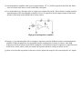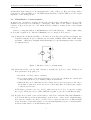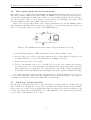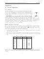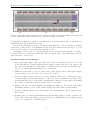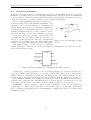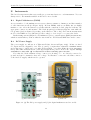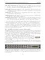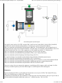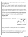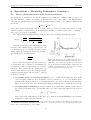
1
20.309 Schedule for Fall 2008
LAB
Lecture 1: Course Overview
Thurs, September 4
Electronics
Fri, September 5
Lecture 2: Voltage dividers and electrical impedance
Reading: H&H p. 3-24
0. Intro to
Lecture 3: Capacitors and RC circuits
Tues, September 9
Electronics
Reading: H&H p. 32-35 and 6.002 notes p. 703-718, 993-1004
Thurs, September 11
|
Lecture 4: Transfer Functions and RC filters
|
Reading: H&H p. 37-40, 46-53 6.002 notes p. 1004-1012, 1030-1054
|
Lecture 5: Thermodynamics of DNA melting
Fri, September 12
Reading: SantaLucia, p. 1460-1462
1. DNA
Lecture 6: Feedback and Amplifiers I
Quiz #1
Tues, September 16
Melting
Reading: H&H p. 163-176 and 6.002 notes p. 1185-1191 HW #1 Due
|
Lecture 7: Feedback and Amplifiers II
Thurs, September 18
|
Reading: 6.002 notes p. 1191-1220
|
Lecture 8: The Reality of Amplifiers
Fri, September 19
|
Reading: TBA
Signals and Systems
|
Lecture 9: Intro to Fourier Analysis
Quiz #2
Tues, September 23
|
Reading: Strang p. 263-275, 309-315
HW #2 Due
Thurs, September 25
|
Lecture 10: Power Spectral Density, Noise and Bandwidth
|
Reading: Press p. 496-500 (on PSD)
|
Lecture 11: Sampling and Discrete Analysis
Fri, September 26
|
Reading: Tutorial and Press p. 500-504 and
|
Lecture 12: Convolution
Tues, September 30
|
Reading: Seung notes (except Sections 3,5,7,8)
HW #3 Due
|
Lecture 13: Application of Convolution Theorem
Thurs, October 2
|
Reading: none
|
DEMO: Thermal Measurement Laboratory
Fri, October 3
Reading: Lab Module #2
2. Thermal
Lecture 14: Mechanical Systems
Quiz #3
Tues, October 7
Measurement
Reading: Strang p. 316-320
HW #4 Due
Thurs, October 9
|
Lecture 15: Ultimate limits of force and position detection
|
Reading: none
|
Student presentations 1
Lab #1 Due
Fri, October 10
|
Laser Safety, Student presentation 2
Tue, October 14
|
HW #5 Due
|
Lecture 16: Optics and Microscopy I
Thurs, October 16
|
Reading: Hecht 2.1-2.9, 4.1-4.5, 5.1-5.3
|
Lecture 17: Optics and Microscopy II
Fri, October 17
|
Reading: Hecht 7.1, 7.3, 9.1, 9.3
Tues, October 21
3.
Lecture 18: Optics and Microscopy III
Fluorescence
Reading: Hecht 10.1, 10.2.1, 10.2.5, 10.2.6
Microscopy
HW #6 Due
|
Lecture 19: Optoelectronics I
Quiz #4
Thurs, October 23
|
Reading: Hecht 13.1-13.1.4
|
Optical Construction; Student presentation 3
Lab #2 Due
Fri, October 24
|
Lecture 20: Optoelectronics II
Tue, October 28
|
Reading: Masters & So 12.1-12.5.7
HW #7 Due
|
|
|
|
|
|
|
|
|
|
4. Project
Labs
|
|
|
|
|
|
|
|
|
|
|
|
Lecture 21: Image Processing I
Quiz #5
Thurs, October 30
Reading: Gonzalas & Wood 4.1-4.4, 8.4.1-8.4.2
Lecture 22: Image Processing II
Fri, October 31
Reading: Gonzalas & Wood 7
Lecture 23: Fluorescence spectroscopy I
Quiz #6
Tue, November 4
Reading: Cantor & Schimel 8.2, p.433-444, Lakowicz, 1.1-1.6
HW #8 Due
Lecture 24: Fluorescence spectroscopy II
Thur, November 6
Reading: Cantor & Schimel 8.2, p.444-465
Final project presentation
Fri, November 7
Lecture 26: Optical trap & Biomechanics
Quiz #7
Thur, November 13
Reading:
HW #9 Due
Student Presentation 4
Lab #3 Due
Fri, November 14
Tue, November 18
Lecture 27: Advanced Fluroescence Microscopy I: Resolution
Reading: Hell, N.Bio, 2003, Rust, N.. Meth. 2006
HW #10 Due
Student Presentation 5
Thur, November 20
Lecture 28: Advanced Fluroescence Microscopy II: Biochemistry
Fri, November 21
Reading: Kim, Nat. Meth. 2007, Jares-Erijman, Nat. Biotech., 2003
Student Presentation 6
Fri, November 25
Lecture 30: 3D Microscopy I: Confocal
Quiz #8
Tue, December 2
Reading: Pawley, 1
Thurs, December 4
Lecture 31: 3D Microscopy II: Multiphoton
Reading: So, Ann Rev 2000, p.400-410, 414-418
Lecture 32: 3D Microscopy III: Demo
Fri, December 5
Student Presentation 7
Tue, December 9
Lab #4 Due
Fri, December 19
20.309 / 2.673 / MAS.402
Biological Instrumentation and Measurement, Fall 2008
Department of Biological Engineering
Massachusetts Institute of Technology
Problem Set #1
Due: Tuesday, September 16
(see Wiki version on the 20.309 website to access on-line links)
1. Wheatstone Bridge The resistor network shown below is known as a Wheatstone bridge. This is a common
circuit used to measure an unknown resistance. Rx is the component being measured, and R3 is a variable
resistor (often called a potentiometer or just a pot for no sensible reason).
a) The bridge is balanced when Vab is zero. Assuming R3 is set so the bridge is balanced, derive an
expression for Rx in terms of R1, R2 and R3.
b) Now let R3 also be a fixed resistor. Suppose that Rx varies in a way that makes Vab nonzero. Derive an
expression for the current that would flow if you connected an ammeter from a to b. Assume the
ammeter has zero internal resistance.
2. Measuring Physical Quantities with a Wheatstone Bridge A thermistor is a resistor whose value varies
with temperature. Thermistors are specified by a zero power resistance, R0, at a given temperature and a
temperature coefficient, α. As shown below, a small person inside the thermistor observes the temperature on a
thermometer and adjusts a variable resistor so that R=R0+αT, where T is the temperature.
Mister Thermistor (with apologies to Horowitz and Hill)
Now imagine a Wheatstone bridge made out of four identical thermistors, as shown in below. One of the
thermistors (R4) is attached to an odd-looking blue apparatus that varies in temperature. The other three are
maintained at a constant 20°C.
Wheatstone Bridge consisting of four thermistors
a) Derive an expression for Vab as a function of temperature.
b) What if both R1 and R4 are attached to the apparatus? Which configuration is more sensitive to
temperature variations?
3. Photodiode I-V Characteristics Using the data that you collected in the lab for the photodiode, generate
three to four i-v curves for a photodiode at different light levels (including in darkness). Plot these on the same
graph to see how incident light affects diode i-v characteristics. Give a brief (qualitative) explanation for why
photodiodes are best used in reverse bias?
4. Unknown transfer functions For the black boxes that you measured in the lab, determine what kind of
circuit/filter each one is (two of them will look similar, but have an important difference - what is it?).
Determine a transfer function that can model the circuit, and fit the model to the data to see whether the model
makes sense. Of the four boxes, "D" is required, and you should choose one of either "A" or "C". You can fit
"B" for bonus credit.
5. Power in a voltage divider Referring to the circuit shown below, what value of RL (in terms of R1 and R2)
will result in the maximum power being dissipated in the load?
Hint: this is much easier to do if you first remove the load, and calculate the equivalent Thevenin output
resistance RT of the divider looking into the node labeled Vout. Then express RL for maximal power transfer in
terms of RT.
A voltage divider formed by R1 and R2 driving a resistive load RL.
20.309 / 2.673 / MAS.402
Biological Instrumentation and Measurement, Fall 2008
Department of Biological Engineering
Massachusetts Institute of Technology
Due: Tuesday, September 23
Problem Set #2
1. Simulation of DNA Melting Lab Refer to instructions located at the class wiki:
http://scripts.mit.edu/~20.309/wiki/index.php?title=Matlab:Simulating_DNA_melting
2. Transimpedence Amplifier Lab Module 0 introduced this op-amp circuit:
Inverting Voltage Amplifier
(a) Calculate the gain of this circuit, Vo/Vi in terms of the input voltage and the two resistor values.
(b) In the DNA melting lab, fluorescence intensity will be determined by measuring the output current of a
photodiode. The schematic below shows a circuit called a transimpedance amplifier that converts a current
to a voltage.
Transimpedence Amplifier
Derive an expression for the output voltage of the circuit produced by a DC current input at iin. (At DC, you
can ignore the affect of the capacitor.) Express your answer in the form of a transfer function, Vout / Iin.
(c) What is the high frequency gain of the transimpedence amplifier? Remember that a capacitor acts like an
open circuit at low frequencies and a short circuit at high frequencies.
(d) A transimpedence amplifier with a gain of approximately 108 V/A will be required for the DNA lab. What
value of resistor in the above circuit would achieve this gain?
(e) It is undesirable to use the large value of resistor you computed in part (d). Shown below is another possible
implementation of the transimpedence amplifier. Derive an expression for the output voltage of this circuit
in terms of the input current and the three resistor values.
High gain transimpedance amplifier
(f) In part (c), you determined the effect of putting a capacitor across the feedback resistor in a transimpedence
amplifier. High gain amplifiers are susceptible to noise coupling from a variety of sources. Since high
frequencies are not of interest in the DNA melting lab, it is beneficial to insert a capacitor to reduce the noise.
In the above circuit, where would you connect the capacitor and how would you choose its size?
(g) Now write down the expression for this new circuit's output with respect to the current input for AC signals.
20.309 / 2.673 / MAS.402
Biological Instrumentation and Measurement, Fall 2008
Department of Biological Engineering
Massachusetts Institute of Technology
Due: Tuesday, September 30
Problem Set #3
(adapted version of problems from Prof Seung, MIT)
1. Fourier series for a sawtooth Define the sawtooth function by s(t) = t / π for –π < t < π
a) In the Fourier series for the sawtooth,
∞
f (t ) = ao + ∑ (an cos ωnt + bn sin ωnt )
n =1
What values does ωn take on? Find the coefficients ao, an, and bn by computing the integrals
T 2
1
ao =
dt. f (t )
T −T∫ 2
T 2
2
an =
dt. f (t ) cos ωnt
T −T∫ 2
T 2
bn =
2
dt. f (t ) sin ωnt
T −T∫ 2
where T = 2 π is the length of the interval (-π, π).
b) Write MATLAB code to sum the first 50 terms of the Fourier series and graph the result in order to verify
that you did the integrals correctly.
2. The Fourier modes as an orthonormal basis Define the inner product of two functions f and g on the
interval [-T/2, T/2] as
2 T2
f , g = ∫ dt. f (t ) g (t )
T −T 2
Show that the Fourier modes 1/√2, cos ωnt, and sin ωnt for ωn = 2πn / T constitute an orthonormal set of functions,
where n ranges over all integers from -∞ to ∞. In other words, verify that the inner product of each function with itself is
unity, and that the inner product of each function with a different function vanishes.
This is why the Fourier modes can be regard as a set of perpendicular axes in the infinite-dimensional space of functions
on the interval [-T/2, T/2]. The formulas for the Fourier coefficients are just projections onto the Fourier modes
(projection is just the term for inner product).
3. Chirp Generate a five second long chirp at a frequency that decays exponentially from an initial value of
1000 Hz with a time constant of τ = 5 seconds,
ν (t ) = 1000e − t / τ
The chirp itself is given by
x(t ) = cos(2πν (t )t )
Use a sampling frequency of 22,050 Hz. Listen to the chirp for fun. Type specgram(x,8192,22050) to
display the spectrogram. If you generated the chirp right, you should see the exponential decay of the frequency
starting from 1000 Hz.
4. Power Spectral Density (PSD) Here we will look at power spectral density in MATLAB using the command
pwelch. To begin, enter help pwelch and become familiar with its parameters. Next, generate a signal
composed of two pure tones with frequencies ν1 = 1000 Hz and ν2 = 1100 Hz:
f (t ) = cos( 2πν 1t ) + cos(2πν 2 t )
using a sampling frequency of fs = 22050 and an interval of 100 μs.
(a) Graph f(t) versus time and then run the commands:
[Pff, freq] = pwelch(f,[],[],[],22050);
loglog(freq,Pff)
Why is there only a single peak?
(b) Play around with the parameters nfft and window until you find a way to make the peaks at 1000 Hz
and 1100 Hz visible. Note that [] denotes the default value.
(c) Now display the spectrum of the square of the signal, f 2. Use the same parameters in the pwelch
command so that all the peaks are visible. You should see that f 2 contains frequencies that were not
present in the original signal. This a mark of a nonlinear system and is called harmonic and
intermodulation distortion by audiophiles. They avoid nonlinearity like the plague.
(d) Find a formula that expresses f2 as a sum of sinusoids. You can think about it as a Fourier series, or just
use trig identities. Use your formula to explain the peaks in the PSD of f2.
(e) In lecture, we used Parseval’s Theorem to show that the mean square average, <f(t)2> is related to the
PSD by
∞
f (t )
2
= ∫ S f (ω )dω
0
where Sf(ω) is the PSD of f(t). Verify that this is the case for f(t) given in this problem. MATLAB’s var
and sum functions will be useful here. Remember that you’re effectively computing the area beneath
the PSD plot so make sure the units match up (pwelch give us you the PSD in units2/Hz).
20.309 / 2.673 / MAS.402
Biological Instrumentation and Measurement, Fall 2008
Department of Biological Engineering
Massachusetts Institute of Technology
Problem Set #4
Due: Tuesday, October 7
1. Discrete convolution Compute the discrete convolution of the two sequences gn and hn given by
gi = [1 1 1 1] (i = 0..3), gi = 0 (else)
hi = [1 1 1 1] (i = 0..3), hi = 0 (else)
a) Do this in MATLAB by shifting, multiplying and adding the appropriate vectors. You may also use the
graphical procedure outlined at the end of this problem set.
b) Check your result using the conv function. Consult the online help (help conv) to find out how to
use this function. Make a stem plot of your result (using stem(…)), and label the x-axis with the
appropriate indices.
2. Convolution theorem applied to NMR This problem uses Nuclear Magnetic Resonance (NMR) signals as
an example to explore some frequently used techniques in measurement and noise analysis.
In NMR one measures the precession of atomic nuclei around and externally applied magnetic field. In
equilibrium, the nuclear spins orient themselves parallel and anti-parallel to the field lines, with a slight
preference towards the parallel orientation. At the beginning of an experiment, an electromagnetic impulse flips
the spins away from their equilibrium orientation, so that their precession induces a time-varying voltage in an
adjacent receiver coil:
The resulting signal has the form
∗
⎧1 ( t ≥ 0)
V (t ) = V0 cos(ω p t )⋅ e −t T u (t ) where u (t ) = ⎨
⎩0 (t < 0)
where ωp = γB0 is called the Larmor frequency (γ = 42 MHz / T for hydrogen). The exponential term accounts
for the fact that the precessing spins rapidly loose their coherence, so that the net signal decays with a
characteristic time constant T* ~ 100ms.
a) Sketch the magnitude of the Fourier transform of V(t) (only qualitatively).
Hint: Use the convolution theorem and the Fourier transforms:
cos(ωpt) → π⋅(δ(ω+ωp) + δ(ω-ωp))
e-t/T*u(t) → (iω+1/T*)-1
You should be able to do this without calculations. Indicate the approximate width of the peaks.
b) The amplitude of the NMR signal is measured by lock-in detection. This means that the rapidly varying
voltage from the receiver coil is multiplied by a frequency and phase matched reference signal Vr(t) and
then low-pass filtered:
Sketch the magnitude of the Fourier transform of the intermediate signal x1 and the output signal x. (Use
graphical convolution or trigonometric identities. There should be three separate peaks in the spectrum).
Copy the transfer function of the low-pass filter shown above to your sketch. What is the purpose of the
low-pass filter?
c) Now we will consider the influence of various noise sources on the measurement. The electrical
resistance R of the receiver coil generates white thermal noise SR. The amplifier contributes some 1/f
noise SA:
Sketch the power spectrum of the output x qualitatively. Assume a cutoff frequency ωLP = ωp/10 for the
low-pass filter. Would the 1/f noise SA be a concern if ωC ~ 1 kHz and B0 = 10 T? Why?
Hint: Since the system is linear, you can first sketch the contributions of V(t), SR, and SA to the power
spectrum of x individually and then add them together.
Graphical approach for taking the convolution of two vectors
The discrete time convolution of the two sequences gn and hn can be found “by inspection” using the following
method:
Draw a stem plot of the two sequences. The x-axis represents the index:
To find the kth point of the convolution (g*h) k (Always leave gn fixed):
1. Mirror the sequence hn about n = 0
2. Shift the mirrored hn to the right by k points e.g. for
3. Multiply the original gn with the modified hn from step 2 point by point, and add the results. For k=2,
this would give you (g*h)2 = 3
20.309 / 2.673 / MAS.402
Biological Instrumentation and Measurement, Fall 2008
Department of Biological Engineering
Massachusetts Institute of Technology
Problem Set #5
Due: Tuesday, October 14
Introduction and Motivation
Force sensors such as the optical tweezers and atomic force microscope (AFM) provide a unique means for
investigating single biomolecules. Examples include the real-time monitoring of enzymatic activity with the
optical tweezers and the direct measurement of forces required to unfold individual protein domains with the
AFM. At the heart of these force sensors is an ultrasensitive displacement detector that resolves the position of
compliant structure (i.e. microcantilever or optically trapped mircobead) with nanometer, or in some cases, subnanometer resolution. The performance of the force sensor is determined by the mechanical properties of the
structure (spring constant, resonant frequency, damping, etc) and the resolution of the displacement detector.
When designing a force sensor for a particular application, it generally desirable to achieve a performance
metric that is thermally limited. In this limit, the noise level of the sensor is governed by kbT.
The goal of this section of the course is to i) understand how the thermal limit of detection is related to the
mechanical properties of the force sensor, and ii) experimentally determine if a force sensor is thermally
limited. The lectures and homework will focus on the first goal while the lab module will focus on the second
one.
As we will see from lectures, the power spectral density (PSD) is a useful function to calculate and measure for
a given sensor. Since we will model the mechanical properties of the force sensor a simple harmonic oscillator
with spring constant k and RMS displacement <x2>, the Equipartition Theorem,
1
1
k bT = k x 2
2
2
tells us that the integral of the position PSD, Sx(f), is directly related to Boltzmann’s constant by
∞
x 2 = ∫ S x ( f )df =
0
T
kb
k
Thus, by measuring the PSD, one can essentially “measure” kb and thereby determine if a force sensor is
thermally limited by comparing it to the known value of 1.38 x 10⁻²³ J/K. This assumes that the temperature
and spring constant are known. Conversely, if a force sensor is known to be thermally limited, one can
determine its mechanical properties by measuring the thermal noise.
Problem
(a) As discussed in the lecture, a harmonic oscillator model for a cantilever can be described by the
differential equation
&x& + 2γx& + ω 02 x = 0 .
Solve for x(t) by assuming the solution is of the form
x(t ) = Ae s1t + Be s2t
where s1 and s2 are roots to the polynomial
s 2 + 2γs + ω 02 = 0
The initial conditions are x(0) = 0 and dx/dt(0) = vo.
(b) The initial conditions can be realized experimentally by accelerating the end of the cantilever with a
very short impulse, vo·δ(t):
h&& + 2γh& + ω 02 h = vo ⋅ δ (t )
where h = h(t) is the impulse response. What is h(t)?
(c) Find the frequency response of the system, ĥ(ω), by taking the Fourier transform of the differential
equation for h(t).
For the remainder of this problem, assume that the cantilever has the following mechanical properties:
Resonant frequency, fo: 10 kHz
Quality factor, Q: 20
Spring constant, k: 0.04 N/m
(d) Plot the magnitude of the frequency response ĥ(ω) on a log-log scale for vo = 0.01 m/s. Make sure to
label your axes with the correct units.
(e) Plot the impulse response, h(t) for a time interval of 10 μs, sampled at a rate of 100 kHz. Again, label
the axes with the appropriate units.
(f) Now assume that the cantilever has an effective mass of m = 10-9 kg and is being driven by a Gaussian
distributed random force F(t) of zero mean and standard deviation <F(t)2>½. Use MATLAB to generate a
25,000 point random vector that represents the acceleration, F(t) / m:
m = 1e-9;
F = randn(25000,1)*1e-6;
g = F/m;
Plot F(t) versus over a time interval of 10 μs, sampled at a rate of 100 kHz.
Verify that F(t) is a white noise signal by plotting the square root of its power spectral density:
fs=1e5;
[PSD,freq] = pwelch(F,[],[],[],fs);
loglog(freq, sqrt(PSD));
xlabel (‘Frequency [Hz]’);
ylabel (‘Power Spectral Density [N / sqrt(Hz)]’);
(g) Find the cantilever response, x(t), by convolving the random noise vector g with the impulse response h.
You may use the conv command to calculate at the convolution integral. Since each discrete point
represents a time interval of 1/fs, you will need to multiply the result of the conv command by 10-5 to
get the correct scaling. Truncate x to the length of the original vector g. Plot the resulting vector x[t]
and the square root of its power spectral density. Use a log-log scale for the PSD.
(h) Now assume the cantilever is thermally driven (ambient temperature is 300 K). Write down the
expression for the PSD of x(t) and plot it on a log-log scale with units Å/√Hz .
(i) Write down an approximate expression for the PSD of x(t) by assuming your measurement bandwidth,
B, is much less than the resonant frequency, fo. Using an ideal position detector (no noise), x(t) is
measured for 1 second and then averaged. What is the smallest change in deflection that could
measured over this interval? What is the minimum detectable force? Give some examples of biological
forces that could be measured with this resultion.
(j) Perhaps the two most useful expressions for the mechanical of beam are the spring constant,
Ewt 3
k=
4L3
where E is the Young’s modulus, t thickness, w width, and L length, and the resonant frequency,
t
E
fo =
2
2πL ρ
where ρ is the mass density. Using these expressions, determine how the minimum detectable force
depends on the microcantilever geometry. This expression is used for designing ultrasensitive force
sensors.
(k) Carefully read Module 2: Atomic Force Microscope with the exception of sections on imaging and
elastic modulus (Sections 3.3.2, 3.3.4, 4, and 5).
20.309 / 2.673 / MAS.402
Biological Instrumentation and Measurement, Fall 2008
Department of Biological Engineering
Massachusetts Institute of Technology
Due: Tuesday, October 24
Lab Assignment #1
Data Analysis
Use Matlab to convert your raw data to fraction hybridized and temperature. Filter the data to remove noise.
This can involve smoothing the data from individual experimental runs as well as combining data from multiple
runs. Plot relative fluorescence versus temperature comparing:
•
•
•
20 bp oligos in solutions of varying ionic strength
Perfect match, single mismatch, and complete mismatch (unknown) 20 bp oligos
40 bp versus 20 bp perfect match oligos
In some cases, it may be helpful to include multiple melting curves on the same plot. Make a table of the
melting temperature Tm for each of these experiments. To accomplish this, you may process the data how you
wish, however a useful command in Matlab is resample. This function can not only resample data, as the name
implies, but will also apply a low-pass filter (decreasing the high-frequency noise). A larger vector of filter
coefficients or number of samples on each side of the current sample will smooth the data more. Using this
command, pay attention to the resulting length of your new data, as well as any inaccuracies at the ends
(consider what resample assumes for the data points before and after your data). Derivatives may require
filtering as well.
Model vs. reality
In class, we derived an expression that relates the melting temperature to the enthalpy change ΔH° and entropy
change ΔS° of the hybridization reaction:
.
Here, f is the fraction of DNA strands hybridized (dimerized) at a particular temperature (at Tm, this is 1/2), and
CT is the total concentration of single-strand oligonucleotides (or 2X the dsDNA concentration when all strands
are hybridized). Choose one of the perfect-match sequences that you measured, and use Matlab to fit the
model to your measured data, which will allow you to extract the ΔH° and ΔS° parameters. To perform the fit,
you will need a Matlab function that will evaluate T(f) given an input const for the ΔH° and ΔS° parameters.
The function will be something like this:
function Tf = melt(const, f)
R=8.3;
C_T=33e-6;
dH = const(1);
dS = const(2);
Tf = dH./(dS - R*log(2*f./(C_T*(1-f).^2)));
You can then invoke matlab's lsqcurvefit routine to do the fit, which will return the best values for ΔH° and
ΔS°.
FitVals = lsqcurvefit(@melt, [dH_guess, dS_guess], frac_vector, temp_vector)
Short questions (please do not use more than two pages for this section)
- What practical problems did you run into?
- Briefly describe (in recipe format) how you processed the raw data. Include the expressions that you use to
make this conversion.
- Do the shapes of your melting curves make sense? (It may be helpful to compare your results to others in the
class)
- Can you identify the unknown samples?
- What factors affect the DNA melting temperature and the sharpness of the melting transition?
Bonus (optional):
Calculate ΔH° and ΔS° for one of the perfet match sequences using the nearest-neighbor model from class.
Compare the calculated values to the best fit parameters. What might explain the differences? What factors
affect ΔH° and ΔS°?
External references (see wiki for links)
•
•
•
National Instruments data acquisition card user manual
SYBR Green I datasheet
LM317 datasheet
20.309 / 2.673 / MAS.402
Biological Instrumentation and Measurement, Fall 2008
Department of Biological Engineering
Massachusetts Institute of Technology
Due: Tuesday, October 24
Lab Assignment #2
Introduction and Motivation
Force sensors such as the optical tweezers and atomic force microscope (AFM) provide a unique means for
investigating single biomolecules. Examples include the real-time monitoring of enzymatic activity with the
optical tweezers and the direct measurement of forces required to unfold individual protein domains with the
AFM. At the heart of these force sensors is an ultrasensitive displacement detector that resolves the position of
compliant structure (i.e. microcantilever or optically trapped mircobead) with nanometer, or in some cases, subnanometer resolution. The performance of the force sensor is determined by the mechanical properties of the
structure (spring constant, resonant frequency, damping, etc) and the resolution of the displacement detector.
When designing a force sensor for a particular application, it generally desirable to achieve a performance
metric that is thermally limited. In this limit, the noise level of the sensor is governed by kbT.
The goal of this section of the course is to i) understand how the thermal limit of detection is related to the
mechanical properties of the force sensor, and ii) experimentally determine if a force sensor is thermally
limited. The lectures and homework will focus on the first goal while the lab module will focus on the second
one.
As we will see from lectures, the power spectral density (PSD) is a useful function to calculate and measure for
a given sensor. Since we will model the mechanical properties of the force sensor a simple harmonic oscillator
with spring constant k and RMS displacement <x2>, the Equipartition Theorem,
1
1
k bT = k x 2
2
2
tells us that the integral of the position PSD, Sx(f), is directly related to Boltzmann’s constant by
∞
x
2
= ∫ S x ( f )df =
0
T
kb
k
Thus, by measuring the PSD, one can essentially “measure” kb and thereby determine if a force sensor is
thermally limited by comparing it to the known value of 1.38 x 10⁻²³ J/K. This assumes that the temperature
and spring constant are known. Conversely, if a force sensor is known to be thermally limited, one can
determine its mechanical properties by measuring the thermal noise.
Lab module requirements
1. Measure the biased z-mod response for the 275 μm and 350 μm cantilevers. Plot the output voltage of
the photodiode as a function as the voltage to the z-mod scanner. Make sure to normalize your data for
any gain applied to your signal downstream of the photodiode output. Include the appropriate units on
your plot.
2. Using the diffraction equation in Section 3.1.2 and accounting for the correction factor described in
Section 3.2.6, plot your data with the abscissa in nanometers (instead of the z-mod scanner voltage).
What is the distance of adjacent minima and maxima? How does this compare to the wavelength of the
illumination?
3. Measure the thermally excited motion for the 275 μm and 350 μm cantilevers. Following the
description in Sections 6.2 and 6.3, plot the Power Spectral Density (PSD) of each cantilever on the
same graph using a log-log scale and units of Angstroms per √Hz for the ordinate. From this plot,
estimate the Quality factor Q and resonant frequency fo of each cantilever.
4. As described in Section 6.1, estimate the spring constant k and the low frequency limit of the
thermomechanical noise, δ, by using the known value of 1.38 x 10⁻²³ J/K for kb. Sketch the magnitude
of δ on your PSD from Part 3 for each cantilever. Does your measurement agree with the low frequency
limit δ? Note that it is common to see ‘1/f’ noise at low frequencies (typically below a few hundred
Hertz for our system) so you will want to make the comparison above this corner point yet below the
resonant frequency.
5. (OPTIONAL) Following the guidelines in Section 6.4, fit the analytical expression of the
thermomechanical noise (without the low frequency approximation) in order to determine Q, fo, and k.
6. For each cantilever, estimate the spring constant (as described in item 3 of Section 6.1) and use your
measured low frequency limit of the PSD (above the 1/f corner and below the resonant frequency) with
the expression of δ to estimate kb.
20.309: Biological Instrumentation andMeasurement Laboratory
Fall 2006
Module 0: Introduction to Electronics
Contents
1 Objectives and Learning Goals
1
2 Roadmap and Milestones
2
3 Lab
3.1
3.2
3.3
3.4
3.5
2
2
4
5
6
6
Procedures
DC measurements . . . . . . . . . . . . . .
Impedance and load . . . . . . . . . . . . .
Photodiode i-v characteristics . . . . . . . .
Time-varying signals and AC measurements
“Black-box” transfer functions . . . . . . .
A Circuit Components
A.1 Resistors . . . . . . . .
A.2 Capacitors . . . . . . .
A.3 Diodes . . . . . . . . .
A.4 Breadboards . . . . . .
A.5 Operational Amplifiers
.
.
.
.
.
.
.
.
.
.
.
.
.
.
.
.
.
.
.
.
.
.
.
.
.
.
.
.
.
.
.
.
.
.
.
B Instruments
B.1 Digital Multimeter (DMM) . . . .
B.2 DC Power Supply . . . . . . . . . .
B.3 Function Generator . . . . . . . . .
B.4 Oscilloscope . . . . . . . . . . . . .
B.5 LabVIEW and the data acquisition
1
.
.
.
.
.
.
.
.
.
.
.
.
.
.
.
.
.
.
.
.
.
.
.
.
.
.
.
.
.
.
.
.
.
.
.
.
.
.
.
.
.
.
.
.
.
.
.
.
.
.
.
.
.
.
.
.
.
.
.
.
.
.
.
.
.
.
.
.
.
.
.
.
.
.
.
.
.
.
.
.
.
.
.
.
.
.
.
.
.
.
.
.
.
.
.
.
.
.
.
.
.
.
.
.
.
.
.
.
.
.
.
.
.
.
.
.
.
.
.
.
.
.
.
.
.
.
.
.
.
.
.
.
.
.
.
.
.
.
.
.
.
.
.
.
.
.
.
.
.
.
.
.
.
.
.
.
.
.
.
.
.
.
.
.
.
.
.
.
.
.
.
.
.
.
.
.
.
.
.
.
.
.
.
.
.
.
.
.
.
.
.
.
.
.
.
.
.
.
.
.
.
.
.
.
.
.
.
.
.
.
.
.
.
.
.
.
.
.
.
.
.
.
.
.
.
7
. 7
. 8
. 8
. 8
. 10
. . . . . . . . .
. . . . . . . . .
. . . . . . . . .
. . . . . . . . .
(DAQ) system
.
.
.
.
.
.
.
.
.
.
.
.
.
.
.
.
.
.
.
.
.
.
.
.
.
.
.
.
.
.
.
.
.
.
.
.
.
.
.
.
.
.
.
.
.
.
.
.
.
.
.
.
.
.
.
.
.
.
.
.
.
.
.
.
.
.
.
.
.
.
.
.
.
.
.
.
.
.
.
.
.
.
.
.
.
.
.
.
.
.
.
.
.
.
.
.
.
.
.
.
.
.
.
.
.
.
.
.
.
.
.
.
.
.
.
.
.
.
.
.
11
11
11
12
12
13
Objectives and Learning Goals
1. Familiarize yourself with standard lab electronics and some common circuit elements: linear
and nonlinear, passive and active.
2. Understand fundamental electronics concepts, including:
• current/voltage dividers
• impedance & load
• frequency response & transfer functions
3. Analyze and build several circuits, which will be of use later.
This module is an extended lab orientation of sorts. Take this time to explore electronic circuits
and really get to know all the features of our lab’s instrumentation. It will pay off later. What you
learn and do this week will underpin many of the experiments during the rest of the semester.
Since you are mainly concerned with understanding your toolset and learning its uses and
limitations, no formal write-up is necessary. However, many parts of this module work hand-inhand with questions on Problem Set 1, so you will still want to record data for completing them.
1
20.309: Biological Instrumentation andMeasurement Laboratory
2
Fall 2006
Roadmap and Milestones
1. Practice making DC and AC signal measurements.
2. Measure circuit input and output impedances and observe loading effects.
3. Study the nonlinear characteristics of a diode, and learn how a photodiode responds to incident light.
4. Test several unknown circuits to determine their transfer functions
3
Lab Procedures
3.1
DC measurements
The simplest type of circuit is the direct current (DC) situation. This means simply that the
applied voltage does not vary in time. Alternating current (AC) is discussed in Sec. 3.4. Most
often, we separate complex signals into their DC and AC components (e.g. a sine wave with a
constant offset) to make analysis simpler.
To get started, wire the circuit shown in Figure 1 on your breadboard, where R1 =330Ω and
R2 =150Ω. Using the power supply, set Vin to 5V. We’ll make a few measurements of the behavior
of R2 in the circuit. We want to know the voltage across it and the current through it.
Figure 1: Resistive voltage divider circuit.
Measuring Voltage with the DMM:
1. First switch the DMM to voltage mode. Note: Make sure that the DMM test leads are
plugged into the right connections. Remember, the correct configurations for current and for
voltage/resistance measurements are different. See Sec. B.1
2. Place the two leads across the terminals of R2 so that it is in parallel as shown in Figure 2.
3. In voltage mode, the DMM has a very large equivalent resistance (ideally infinite) so that
when placed in parallel with the circuit you are measuring, it will have minimum effect on
the circuit under test.
To prove this:
(a) Assume first that the effective resistance of the DMM is small, such as 100Ω. What is
the combined resistance of the parallel combination of R2 and the DMM?
(b) Now assume the DMM’s resistance is something very large, like 10MΩ. Now what is the
resistance of the parallel combination of R2 and the DMM?
2
20.309: Biological Instrumentation andMeasurement Laboratory
Fall 2006
Figure 2: Measuring voltage across R2 .
Why would a DMM in voltage mode with low input resistance be poor for voltage measurements? Hint: think about how it affects the voltage divider circuit in this case.
Measuring current with the DMM:
1. Switch the DMM to current mode.
2. Place the leads of the DMM in series with a device in the path that you want to measure,
shown in Figure 3. For this type of measurement you actually need to break the circuit and
insert the DMM.
Figure 3: Measuring current through R2 .
3. What would you expect to happen if you reverse the leads of the DMM? Reverse the leads
and see if you were correct.
4. The input resistance of the DMM in current mode is very small, ideally zero. Why is it
important for the effective resistance of the DMM to be small in current mode? Again think
about the effect on the circuit under test.
Calculate the resistance of R2 using Ohm’s law and the current and voltage you measured. Also
determine the error in the nominal resistance value:
error = 100 ×
Rexp − Rmeas
.
Rexp
Is this within the tolerance value indicated by the color bands on the resistor?
3
20.309: Biological Instrumentation andMeasurement Laboratory
Fall 2006
Measuring resistance with the DMM:
1. Turn off power to the circuit, and disconnect the resistor you want to measure. This is
important both in order to protect the DMM and because other parts of the circuit will affect
the resistance you measure for one particular branch.
2. Switch the DMM to resistance mode.
3. Place the leads in parallel with the resistor of interest (in this case R2 ), as you did for the
voltage measurement in Figure 2. Does this match your calculated resistance?
Resistor i-v characteristics
The current-voltage (i-v ) curve of a circuit element is simply a plot of the current through it as a
function of applied voltage. In your lab notebook, sketch the i-v curve of the resistor you measured.
What is the slope of this curve? (Ohm’s law should make this very easy).
3.2
Impedance and load
From the previous section you already have a sense of the importance of considering the equivalent
impedances of your instruments – when making voltage or current measurements (or connecting
any two circuits together) we must always keep in mind the relative output and input impedance of
these components.
An easily observable example: Suppose you have a 5V power
source, and need to drive an LED with approximately 2 volts. A
voltage divider may seem straightforward to use for this purpose,
but one must be careful when designing the circuit. To see why,
wire up the circuit in Fig. 4, first using relatively small resistors
(50-500Ω range), then do it using resistors that are 100× larger.
• Why does the brightness of the LED change so drastically?
• Measure the voltage at the + node of the LED, before hooking it up, and after. Also, measure the current through the
LED in each case. Does this help you understand what’s
going on?
Figure 4: A voltage divider
• Calculate the output impedance of the driving voltage di- driving an LED.
viders in the two varieties you built.
A brief discussion:
Impedance is a generalization of resistance (including capacitance and inductance), and we use the terms somewhat interchangeably here, but you should know
that they are not strictly speaking the same.
A load is a general way of referring to any part of a circuit that has a signal delivered to it,
such as a measurement device, or a particular component. What is considered the “load” depends
entirely on how the parts of the circuit are being considered. In the case of the circuit in Fig. 4
the LED is the load for the voltage divider.
The output impedance of a circuit or device is seen “looking into” the output port of a circuit (i.e.
between the output signal node and ground). Likewise, the input impedance of a device/circuit is
the impedance seen between the input node and ground. The agent doing the “seeing” is whatever
connects to the circuit in question – e.g. if an oscilloscope is hooked up to a circuit to do a
4
20.309: Biological Instrumentation andMeasurement Laboratory
Fall 2006
measurement, that circuit “sees” the input impedance of the oscilloscope. Here, the voltage divider
being used to drive the LED “sees” the LED’s input impedance, and the LED “sees” the output
impedance of the driving circuit.
3.3
Photodiode i-v characteristics
In this section, our aim is to measure and plot the current-voltage relationship for a diode in the
transition region from non-conducting to conducting. After that, we also want to measure the
behavior of photodiodes (see Sec. A.3, which we’ll use a number of times in the course as light
detectors.
Start by covering the window of an FDS100 photodiode with black tape — with no light coming
in, it is just a regular diode. Then we’ll illuminate it to see its photodiode action.
(A) Construct the circuit shown in Fig. 5. You have at your disposal your DC power supply, and
a variable resistance R (we recommend you use values of 100kΩ, 27kΩ, 8.2kΩ, 4.7kΩ, 2.2kΩ,
and 820Ω — this is more straightforward than using a pot and measuring its value every time
you turn the knob).
Figure 5: Circuit for diode i-v measurements.
(B) Given this circuit, come up with a scheme to measure the diode’s i-v curve. Think about
these questions to help guide you:
• Is current or voltage easier to measure?
• For a given setting of VS and R in Figure 5, how can you calculate the current and
voltage through the diode by making a single measurement?
• What should you do differently for the forward and reverse bias regions of the curve?
From what you know about diodes, how does their impedance in forward bias compare
to that in reverse bias?
You’ll want to generate a set of ID and VD values in your notebook to be used for creating
the i-v plot. Then put a plot together using the program of your choice (MS Excel is fine).
(C) For photodiode behavior, uncover the window of the device, and aim a Fiber-Lite illuminator
at it. You should repeat the measurements you made at two or three levels of light intensity.
You can now combine your data to produce four i-v curves for this diode at different light
levels. Plot these on the same graph to see how incident light affects diode i-v characteristics.
You’ll need this data for your first Homework Set.
5
20.309: Biological Instrumentation andMeasurement Laboratory
3.4
Fall 2006
Time-varying signals and AC measurements
Generally, we refer to signals that vary with time as AC signals (alternating current, as opposed to
DC - direct current). When we leave DC behind, the DMM we’ve used so far is no longer enough to
observe what is happening. At this point, you’ll need to get acquainted with the function generator
(Sec. B.3) and the oscilloscope (Sec. B.4), to generate and record AC signals, respectively. We’ll
also start making extensive use of BNC cables and connectors.
First, let’s look at how the resistive voltage divider with which you’re already familiar behaves
with AC signals. Build the divider circuit as you did in Sec. 3.1, but use the function generator in
place of Vin , and the oscilloscope in place of the DMM (Figure 6).
Figure 6: The familiar divider circuit, with a voltage measurement across R2 .
1. Set the FG503 frequency to 5kHz, and the waveform to sinusoid with no offset.
2. Set the voltage to 3V peak-to-peak (often written as 3Vpp ). Verify that the voltage is set as
you intend with the scope, since the FG503 has no markings on its knob.
3. Connect the waveform to your circuit.
4. Use the other channel of the scope to measure Vpp across R2 . Also measure the frequency
across R2 on the scope. You can display both the input and output waveforms at the same
time by using the scope’s dual mode. Does this resistive voltage divider behave any differently
at AC than it did at DC? What’s the relationship between the output and input waveforms?
Now replace R2 with a capacitor in the 0.05-0.1 µF range. Again use dual mode on the scope
to see both the input and output waveforms. Qualitatively observe what happens to the output as
you change the frequency of the input. What kind of circuit is this?
3.5
“Black-box” transfer functions
For this part, you’ll find prepared for you several metal boxes with “mystery” circuits wired up
inside, labelled “A” through “D.” Your goal is to determine their transfer functions. To streamline
the process, we’ve provided a program that will output a frequency-sweep function, which you can
feed into the circuit. The program will then record the amplitude of the output, and plot the data
for you. Ask your lab instructor how to use it.
6
20.309: Biological Instrumentation andMeasurement Laboratory
Fall 2006
Appendices
A
Circuit Components
A.1
Resistors
The important things to know about resistors are: (1) value, (2) tolerance,
and (3) power rating. The power rating indicates the maximum amount of
power a resistor can withstand, e.g. 1/4 watt, 1/2 W, etc. The value and the
tolerance of the resistor is printed on the package in the form of a color-band
code (see below).
Potentiometers (or “pots”) are variable resistors with three leads. The
top half of Figure 7 shows a full schematic, but the lower picture is usually
used for compactness. The arm at lead #2 is called the wiper, and turning
the potentiometer knob controls its position. While the resistance between
#1 and #3 always remains the same, the knob varies the resistance between
leads #1 and #2 (and between #2 and #3). Another way to think of this is
as a variable voltage divider. The value between either #1 and #2 or #2 and
#3 can be varied from zero to the pot’s full value.
Figure 7:
Two
ways potentiometers are shown on
schematics.
Reading the Resistor Color Code
We provide this table here for your convenience, but you can always easily look this information
up on the web. For instance, http://www.elexp.com/tips/clr code.gif contains a good table
of 4-band and 5-band resistor color codes, while this URL does it in an interactive clickable Java
applet: http://samengstrom.com/elec/resistor/index.html.
1. Orient the resistor so that the band that is most separated from the rest is on the right
(typically this is gold or silver).
2. On a four-band resistor, form the number from the first and second band by placing them as
the tens and ones place respectively (e.g. from the left a blue band then a green band means
65).
Color
Black
Brown
Red
Orange
Yellow
Green
Blue
Violet
Gray
White
Gold
Silver
First or Second
Band (digit)
0
1
2
3
4
5
6
7
8
9
Third Band
(multiplier)
1
101
102
103
104
105
106
107
108
109
0.1
0.01
Fourth Band
(tolerance)
1%
2%
0.5%
0.25%
0.10%
0.05%
5%
10%
Table 1: Table of 4-band resistor colors. For a five-band resistor, the first band becomes the 100s
digit, the second band is the tens the third the ones, the fourth is the multiplier, and the fifth the
tolerance.
7
20.309: Biological Instrumentation andMeasurement Laboratory
Fall 2006
3. Multiply the resulting number by the multiplier from the third band (e.g. blue-green-red =
65 × 100 = 6.5kΩ).
4. The most common types of resistors are 5% and 1%, so for quick designation the bodies of
these resistors are often color coded (brown – 5% and blue – 1%).
A.2
Capacitors
Capacitors immediately make for much more interesting types of circuits than simple resistive
networks, because (1) they can store energy and (2) their behavior is time-dependent.
An intuitive way to think about capacitor behavior is that they are reservoirs for electrical
charge, which take time to fill up or empty out. The size of the reservoir (the capacitance C) is
one of the factors that determines how quickly or slowly. Because of this, circuits with capacitors
in them have time-dependent and frequency-dependent behavior. Capacitors act like open circuits
at DC or very low frequencies, and like short circuits at very high frequencies.
A.3
Diodes
This is one of the simplest non-linear electronic devices, and is remarkably versatile. It can function
as an electronic “valve”, as a light-emitter (LED) or a light-detector (photodiode). Fig. 8 shows
how they appear on schematics.
A diode as an electrical “valve.” In the simplest model, we can imagine
a diode as a one-way electrical valve - it behaves almost as a short circuit (wire)
when a positive voltage is applied across it (called forward bias – shown in Fig. 8)
and as an open circuit with a negative voltage (reverse bias). As you might guess,
this is not the whole story, and is only true for relatively large voltages. You will Figure 8: The
explore diode behavior in more detail, especially around the critical transition diode symbol
region near 0 volts.
on a schematic.
Photodiodes are optimized to work as a light detector by capturing photons
and converting them to electrical signals. This happens when photons absorbed in the semiconductor generate electron-hole pairs. Run in reverse bias, the current out of the photodiode is linearly
proportional to the light power striking the device.
Light-emitting diodes (LEDs) are designed to output light when current passes through
them. In this case, we have recombination of electron-hole pairs producing photons in the semiconductor. Light is emitted in forward bias, and power output depends on the current flowing through
the device (what’s the relationship? linear? quadratic?).
A.4
Breadboards
Breadboards are a platform that allows for easily building prototype circuits without the need
for soldering. Their advantage is that parts can be added, swapped in and out, and different
configurations tested very easily and quickly. However, breadboards are bulky, pick up significant
excess noise from the environment, have large parasitic capacitance, as well as other limitations.
Once a circuit design is finalized, it’s typically made in a printed circuit board (PCB).
Figure 9 is an example of a breadboard, where each square represents a hole in which a wire
lead can be placed. The lines drawn over the board represent the basic connectivity. The two
outermost lines on each side represent power “buses” that are connected across all rows. In the
very center of the board is a divider that separates columns A-E and F-J. Each row is connected:
i.e. 1A-E are all connected to each other, as are 1F-J. However, A-E are electrically isolated from
8
20.309: Biological Instrumentation andMeasurement Laboratory
Fall 2006
Figure 9: A typical breadboard layout. Some breadboards have several panels such as these adjacent
to each other, with banana cable jacks for power and ground connections.
F-J. Finally, rows that are not in the power rail are also electrically isolated (these connections are
explicitly shown only in the first five rows).
Of course, if connectivity is unclear, you can use the multimeter to test for electrical continuity
between two points on the board. Multimeter leads often don’t fit in the holes directly, so you can
use a wire as a connector between the meter and the board.
An example of how to place a component in the breadboard is shown in the figure. A resistor
is depicted as a red box with two metal leads. There are many ways to place this resistor, and the
figure shows two of these ways.
Breadboard Tips and Techniques
1. Choose the right length of wire and clip leads to keep components and wires close to the
board. This has two benefits: (1) It makes debugging a circuit easier if you can easily see all
the connections and (2) It prevents pick-up of additional noise from the environment, since
big loops of conducting material make for good antennas.
2. Utilize the power rails, e.g. use one each for the positive supply voltage and negative supply
voltage (referred to as +Vcc and −Vcc ), and one for ground.
3. Create a common ground. If you use a power supply for DC power, a function generator
for an AC supply, and measure using the oscilloscope, then you will have four independent
grounds that may not be at the same potential unless connected together (the four grounds
are: circuit ground, FG ground, PS ground, and scope ground).
4. Always turn off power when building and making any changes to the circuit. Also, when
measuring resistance, power off the circuit and disconnect the resistor being measured.
5. As a rule of thumb, always connect the ground lead of an instrument to the circuit first before
the live lead.
6. In future labs, we will work with Integrated Circuit (IC) packages. Static electricity can
destroy ICs. To prevent damage, ground yourself before handling them by touching a metal
object, e.g. a metal case or metal bench top.
9
20.309: Biological Instrumentation andMeasurement Laboratory
A.5
Fall 2006
Operational Amplifiers
In the upcoming lab module we will start using integrated circuits (ICs) known as operational
amplifiers, or op-amps. They are an enormously versatile circuit component, and come in hundreds
of special varieties, built to have particular characteristics and trade-offs. We will use some very
common general-purpose op-amp, of which a typical example is the LM741.
Every op-amp manufacturer provides a datasheet for every IC they make, and you should always familiarize yourself with it. It provides information on everything from
pin and signal connections, to special features, limitations,
or applications of a particular IC. We have copies of the
datasheets available in the lab for the op-amps we are using, and you’ll want to refer to them regularly as you work.
As you’ll see in lecture, a typical op-amp circuit looks
something like Fig. 10. This is called the inverting configuration, because the input is connected to the inverting
(–) input. As you might guess, the output signal is the Figure 10: A basic inverting op-amp
negative of the input, times a gain factor set by the circuit. circuit.
The LM741 package of course does not look like the
triangle drawn above. Instead it looks more like Figure 11. Plugged into a breadboard, the two
rows of pins straddle a trough.
Figure 11: The pin assignments of the LM741 in a DIP-8 package.
Besides the (–) and (+) (inverting and non-inverting) inputs, an op-amp needs DC power
connections, which is what enables it to be an active circuit element. These power connections are
usually omitted on a schematic (as in Fig. 10), but always shown on the datasheet (in Fig. 11 they
are pins 4 and 7). Typically ±15 volts is used, but you should check the datasheet to be sure.
Every IC has a marking on the package to indicate Pin 1, and the datasheet shows the relative
positions of the other pins. On your LM741 there is a dot near Pin 1 (or a semi-circle on one end
of the chip, as in the figure to the right). nc on the datasheet stands for No Connection.
Important:
ICs are sensitive to static electricity discharges. Your body can easily store
enough charge to damage an IC, especially on a dry winter day. To prevent this, always make
sure to touch the grounded metal case of an instrument to dissipate the charge. Use caution when
handling the chips.
10
20.309: Biological Instrumentation andMeasurement Laboratory
B
Fall 2006
Instruments
The brief descriptions in this section will give you an introduction to each instrument. You can
always refer to the manuals available in the lab for more details.
B.1
Digital Multimeter (DMM)
A very versatile tool, the multimeter serves as a voltmeter, ammeter, ohmmeter, and has a number
of other functions as well (see Figure 12(b)). Modern DMMs, such as our Fluke 111, are highly
intuitive to use: select the function you want with the central mode dial, plug the leads into the
appropriate connectors, and measure. The black (negative) lead always plugs into com while the
red (positive) lead is adjusted depending on the function. The voltage and current measurement
modes of the DMM are very different (you’ll see why), so don’t forget to reconnect the leads.
In alternating current (AC) mode, the multimeter gives root-mean-square (RMS) measurements,
which are useful when you know what the waveforms are. We’ll discuss RMS later in the course.
B.2
DC Power Supply
The power supply we will use is a Tektronix PS503, shown in Figure 12(a). It has one fixed
5V output and two adjustable ones. The (+) and (–) outputs have adjustable current limits
and voltages up to ±20V can be set either independently, or together (using the dual tracking
knob). The white output button on the upper right allows power to flow to the outputs: always
remember to turn this off or disconnect it when rewiring your circuits.
Note that the black common voltage connector is “floating,” i.e. not directly connected to
ground, and can’t be assumed to have zero voltage. You’ll want to connect it to the white connector
of the fixed 5V supply, which is tied to ground.
(a) Tektronix PS503A.
(b) Fluke 111.
Figure 12: (a) The DC power supply and (b) the digital multimeter used in our lab
11
20.309: Biological Instrumentation andMeasurement Laboratory
B.3
Fall 2006
Function Generator
A function generator does what its name says — generates signal waveforms for standard functions: sinusoids, triangles, square waves. The FG503 is very
basic. Its frequency range is about 0.1Hz to 300kHz,
and amplitude range from about ±0.35V to ±10.0V.
It can output waveforms with and without offset. The
large central dial in Figure 13 is the main frequency
knob, which sets the output frequency together with
the multiplier knob (labeled). Be warned that the
large dial’s markings can be fairly inaccurate – always verify the actual output frequency with an oscilloscope or spectrum analyzer.
Note that higher-end function generators, such as
the DS-345 from Stanford Research Systems, have
much more precise controls for waveform frequency,
amplitude, and offset, and may have other advanced Figure 13: An FG503 function generator.
features like sweeping frequency, generating nonstan- (In this image, the BNC signal connectors
dard or arbitrary waveforms, and modulation.
are capped.)
B.4
Oscilloscope
An oscilloscope is designed for observing signal waveforms that change faster than can be usefully
seen on a DMM. Most often, the signals observed are periodic, and the scope is effectively a “time
magnifier” letting you stretch and compress the timebase (as well as the waveform magnitude) for
convenient viewing.
Ours is an OS-5020 model made by EZ Digital, the front panel of which is shown in Figure 14.
It’s about as basic as a two-channel analog scope can be. Below is a brief description of the most
important controls:
Figure 14: The OS-5020 oscilloscope.
12
20.309: Biological Instrumentation andMeasurement Laboratory
Fall 2006
CH1, CH2: channel inputs (2) - Signals connect to these via BNC cables. Above each input
is a three-position input coupling switch (ac - gnd - dc). Understanding the three settings
is crucial to knowing how the scope is measuring incoming signals.
VOLTS/DIV: channel gain knobs (2) - Set the “magnification” of the waveform in the vertical axis. The scale around the knob tells you how many volts each square of the grid represents
at a given magnification.
MODE select - Choose whether the scope is displaying the signal on Ch. 1, Ch. 2, both simultaneously (dual), or their sum (add).
POSITION knobs (2 vert., 1 horiz.) - Set the zero-position of the trace for each channel, and
the time-trace to enable accurate measurements.
TIME/DIV: timebase selector - Like channel gain, but for the horizontal (time) axis, this sets
how much time each square of the grid represents. In its rightmost position, it selects “X-Y
mode”, which plots the two input channels one vs. the other, with no time dependence.
Most of the other controls deal with triggering, which refers to synchronizing the scan of the
display with the input waveform. You will get a feel for these as you use the instrument in lab.
You’ll notice that the scope only measures voltages – there are no modes for directly measuring current or resistance. It’s also important to remember that scope measurements are always
referenced to ground. The shield (black lead when using grabber wires) of the BNC connector is
hard-wired to ground. This means you can’t use just one channel of a scope to measure the voltage
between two non-ground nodes in a circuit.
B.5
LabVIEW and the data acquisition (DAQ) system
LabVIEW is a software and hardware system designed to perform the functions of many standard
bench-top measurement devices. The hardware provides signal input and output for the PC (see
Fig. 16, while the software runs what are called “virtual instruments” (VIs), resulting in a very
general-purpose data collection and processing platform. In addition to collecting data, LabVIEW
can be used to control instruments, for example via a GPIB interface.
You will use a number of different VIs throughout the course that have been
written for you. While they will all perform different functions, they all have
common run/stop controls in the upper left hand corner, as shown in Fig. 15.
The arrow at the left is used to start each VI, and the red ”stop” button will halt
Figure 15:
it once it is running.
The great advantage of LabVIEW is its breadth and flexibility. The major disadvantage is that
when performance is important (high speed, low noise, high precision, etc.) dedicated instruments
quickly outperform it.
Figure 16: The data acquisition (DAQ) connection board, used for signal input and output with
LabVIEW. The analog input channels are in two rows, labeled ach0 through ach7, and ach8
through ach15. The two output channels are to their right, labeled dac0out and dac1out, one
above the other.
13
20.309:Measuring DNA Melting Curves - OpenWetWare
1 of 12
http://www.openwetware.org/wiki/20.309:Measuring_DNA_Melting_C...
20.309:Measuring DNA Melting Curves
From OpenWetWare
Contents
1 Introduction
1.1 Overview of the apparatus
1.2 Objectives and learning goals
2 Lab procedure
2.1 Roadmap
2.2 Optical system
2.2.1 Illumination
2.2.2 Fluorescence detection
2.3 Electrical System
2.4 LED driver
2.5 Temperature
2.6 Fluorescence intensity
2.6.1 Amplification circuit
2.6.2 Offset circuit
2.7 Practical matters
2.8 PC Data Acquisition System
2.8.1 LabVIEW VI
2.9 Debugging the apparatus
3 Experimental procedure
3.1 Prepare your apparatus
3.2 Make a sample
3.3 Heat up the sample
3.4 Transfer the sample to your apparatus
and take data
4 Report Requirements
4.1 Data Analysis
4.2 Model vs. reality
4.3 Discussion
5 External references
DNA Melting Apparatus
Introduction
8/13/2008 9:34 AM
20.309:Measuring DNA Melting Curves - OpenWetWare
2 of 12
http://www.openwetware.org/wiki/20.309:Measuring_DNA_Melting_C...
Example DNA melting curves showing the
effect of varying ionic strength. The data
has been filtered to reduce noise.
Differentiating the melting curve simplifie
finding Tm.
In this lab, you will measure the melting temperature of several DNA samples to determine the effect of sequence
length, ionic strength and complementarity. A common application of this technique exploits the length dependence o
DNA melting temperatures to examine PCR products in order to determine whether a desired sequence was
successfully amplified.
The measurement technique utilizes a fluorescent dye that binds preferentially to double stranded DNA (dsDNA). Thi
characteristic of the dye allows the relative concentration of dsDNA to be determined by measuring the intensity of
fluorescent light given off by an excited sample.
The DNA melting apparatus you will construct consists of four major subsystems: excitation, fluorescence
measurement, temperature sensing, and data acquisition. You will build these subsystems out of an LED, a photodiode
a resistance temperature detector (RTD), and a PC data acquisition system.
The goal of your time in the lab will be to measure fluorescence intensity versus temperature for each of the samples
over a range of about 90°C to room temperature. This will provide a basis for estimating the melting temperature, Tm
of each sample. (Tm is defined as the temperature where half of the DNA in the sample remains hybridized.)
Three of the samples will be unknown. All the unknowns will have the same length, but different degrees of
complementarity: complete match, single mismatch, and complete mismatch. Using the data you gather, you will
attempt to identify these three samples.
8/13/2008 9:34 AM
20.309:Measuring DNA Melting Curves - OpenWetWare
3 of 12
http://www.openwetware.org/wiki/20.309:Measuring_DNA_Melting_C...
Overview of the apparatus
In most DNA melting apparatuses, the temperature of the sample is ramped up at a controlled rate and the concentratio
of dsDNA recorded. In our homebrew setup, however, we will first heat up the sample in a bath. That way, natural
cooling will provide the range of temperature conditions needed. As the sample cools, a PC data acquisition card will
record the photodiode and RTD outputs over time. During data analysis, you will convert these voltages to temperatur
and relative dsDNA concentration. The melting temperature, Tm can be estimated from a graph of this data or its
derivative.
SYBR Green I (http://www.sigmaaldrich.com/sigma-aldrich/datasheet/s9430dat.pdf) is most sensitive to blue light wi
a wavelength of 498 nm. The dye emits green light with a wavelength of 522 nm. You can easily observe this – a
room-temperature sample of dsDNA and SYBR green looks yellow from the combination of blue excitation and green
fluorescence. At higher temperatures, when there is no dsDNA to bind to, the sample will appear blue or clear.
As shown in the diagram, an aluminum heating
block holds a cuvette containing the sample
under test. The sample is a combination of
DNA and a fluorescent dye called SYBR
Green. In addition to being a convenient
holder, the block gives the setup enough
thermal inertia to facilitate a measurement from
natural cooling. (Without the block, the sample
would cool too quickly.)
Blue light from an LED illuminates one side of
the cuvette. An optical filter shapes the output
spectrum of the LED so that only the desired
wavelengths of light fall on the sample.
A photodiode placed at 90 degrees to the LED
source detects the green light emitted by bound
SYBR Green. The photodiode is placed behind
an optical filter to ensure that only the
fluorescent light given off by the sample is
detected.
The DNA melting apparatus includes excitation, fluorescence
measurement, temperature sensing, and data acquisition functions.
Since photodiodes produce only a very small
amount of current, it will be necessary to build a very high gain transimpedence amplifier to produce a signal that is
measurable by the PC data acquisition cards. Photodiode amplifiers are particularly challenging because many of the
non-ideal characteristics of op amps become apparent at high gain.
An RTD attached to the heating block and wired to a voltage divider provides an indication of temperature. The
temperature of the heating block will be a proxy for the sample temperature. Unfortunately, the block cools faster whe
it is hot than when it is near room temperature. You will have to get the heating block set up in your apparatus quickly
after you remove it from the heating block.
A PC data acquisition card digitizes the amplified photodiode and RTD signals. A LabVIEW virtual instrument (VI)
records the signals over time. Data from the DNA melting VI can be saved to a file. The file can be loaded into Matlab
for analysis.
Objectives and learning goals
8/13/2008 9:34 AM
20.309:Measuring DNA Melting Curves - OpenWetWare
4 of 12
http://www.openwetware.org/wiki/20.309:Measuring_DNA_Melting_C...
Measure temperature with an RTD.
Implement a high gain transimpedence amplifier for photodiode current multiplication.
Measure light intensity with a photodiode.
Build an optical system for exciting the sample with blue light and gathering the fluorescence output on the
photodiode.
Record dsDNA concentration versus temperature curves for several samples.
Estimate Tm from your data.
Compare the measured curves with theoretical models.
Identify unknown DNA samples.
Lab procedure
Roadmap
1.
2.
3.
4.
5.
6.
7.
Build an optical system containing the LED, heating block, sample, photodiode, filters, and lenses.
Hook up a three terminal voltage regulator to create an electrical power supply for the LED.
Build, test, and calibrate the temperature-sensing circuit.
Build an amplification/offset circuit for the DNA fluorescence signal.
Troubleshoot and optimize your system.
Heat a samples of DNA with SYBR Green dye and record DNA melting curves as the samples cool.
Analyze the data. Identify the three unknown samples. Compare your observations to theoretical models.
Optical system
8/13/2008 9:34 AM
20.309:Measuring DNA Melting Curves - OpenWetWare
5 of 12
http://www.openwetware.org/wiki/20.309:Measuring_DNA_Melting_C...
DNA Melting Optical System Diagram
The optical system consists of an LED, excitation filter, sample cuvette, heating block, emission filter, photodiode,
optional lenses, and associated mounting hardware. Construct your system on an optical breadboard
(http://www.thorlabs.com/thorProduct.cfm?partNumber=MB1224) . The breadboard has a grid of tapped holes for
mounting all kinds of optical and mechanical hardware. ThorLabs (http://www.thorlabs.com) manufactures most of th
hardware stocked in the lab. A few of the components you will certainly use include: 1/2" diameter posts
(http://www.thorlabs.com/newgrouppage9.cfm?objectgroup_id=1266) , CP02 cage plates
(http://www.thorlabs.com/thorProduct.cfm?partNumber=CP02) , and 1” diameter lens tubes
(http://www.thorlabs.com/NewGroupPage9.cfm?ObjectGroup_ID=1521) .
Use optical rails (http://www.thorlabs.com/thorProduct.cfm?partNumber=RLA0300) and rail carriers
(http://www.thorlabs.com/thorProduct.cfm?partNumber=RC1) or optical bases
(http://www.thorlabs.com/NewGroupPage9.cfm?ObjectGroup_ID=47) to mount 1/2” posts on the breadboard. RA90
(http://www.thorlabs.com/thorProduct.cfm?partNumber=RA90) right angle post clamps and post holders
(http://www.thorlabs.com/thorProduct.cfm?partNumber=PH2-ST) can also be useful.
There are a variety of ways to construct the apparatus. A good design will be compact, stable, and simple. It will be
necessary to shield the optical system from ambient light, so a small footprint will be advantageous.
Illumination
Begin by mounting the LED on your breadboard. Note that there are two styles of LEDs. The Lamina LED Array
(http://www.laminaceramics.com/docs/BL_2_Blue.pdf)
is mounted on an aluminum heat sink and bolted to a CP02 cage plate. The CP02 attaches to the top of a post. It has an
SM1 threaded hole through the middle that connects to 1” diameter lens tubes. The Cree LEDs
8/13/2008 9:34 AM
20.309:Measuring DNA Melting Curves - OpenWetWare
6 of 12
http://www.openwetware.org/wiki/20.309:Measuring_DNA_Melting_C...
(http://www.allelectronics.com/spec/LED-112.pdf) are already mounted in a 1” lens tube.
Both styles of LED emit a range of wavelengths with a peak at 475 nm. A Chroma Technology D470
(http://web.mit.edu/~20.309/Students/Datasheets/Chroma%20D470-40.pdf) filter eliminates unwanted parts of the
spectrum that might interfere with detection of the fluorescence signal. The filters have exposed, delicate coatings and
must be handled carefully (http://www.chroma.com/index.php?option=com_content&task=view&id=56&Itemid=65)
In addition, the filter works better in one direction than the other
(http://www.chroma.com/index.php?option=com_content&task=view&id=57&Itemid=66) .
Light from both kinds of LEDs diverges in a cone with an angle of about 100 degrees, so place the device close to the
sample. You can also use a lens to concentrate the LED's output. Several lenses are available in the lab:
f=25.4mm (http://www.thorlabs.com/thorProduct.cfm?partNumber=LA1951)
f=50mm (http://www.thorlabs.com/thorProduct.cfm?partNumber=LA1131)
f=100mm (http://www.thorlabs.com/thorProduct.cfm?partNumber=LA1509)
f=200mm (http://www.thorlabs.com/thorProduct.cfm?partNumber=LA1708)
Fluorescence detection
The SM05PD1A (http://www.thorlabs.com/Thorcat/8700/8770-D02.pdf) photodiode is mounted in a short tube with
SM05 threads. Use a SM1A6 (http://www.thorlabs.com/thorProduct.cfm?partNumber=SM1A6) adapter to mount the
photodiode in a CP02 cage plate. Mount the photodiode assembly to the breadboard at 90 degrees to the LED. Build a
system to hold the Chroma E515LPV2 (http://web.mit.edu/~20.309/Students/Datasheets/Chroma%20E515lpv2.pdf)
emission filter in front of the photodiode. You can use a lens to focus light from the sample on to the detector to
improve performance, if you like.
Put an optical quick connect at the end of the photodiode assembly to facilitate easy attachment of the heating block
during experimental runs. The other half of the quick connect goes into the CP02 cage plate mounted on the heating
block.
Electrical System
LED driver
Or: how to make a current source
Drive the LED array with an LM317T
(http://www.national.com/ds/LM/LM117.pdf) variable voltage regulator as
Current feedback to the adjust pin of the
LM317T variable voltage regulator
provides a steady source of illumination.
(Note that 4.2Ω should read 4.3Ω)
shown. The LM317T has a feedback circuit that strives to maintain 1.25 volts between its output and adjustment pins.
Thus, in the circuit shown, the LM317T sources a constant current of approximately .29A through the load (and the
feedback resistor).
8/13/2008 9:34 AM
20.309:Measuring DNA Melting Curves - OpenWetWare
7 of 12
http://www.openwetware.org/wiki/20.309:Measuring_DNA_Melting_C...
It is possible to drive an LED with a voltage source; however, the steepness of a diode's I-V curve results in large
current swings for small changes in supply voltage. LED brightness is proportional to current. A current source will
provide a more stable light output.
The LM317T and 4.3Ω resistor both dissipate quite a bit of power in this connection. They will become toasty. Use a
heat sink on the LM317T. Double check your wiring before connecting the LED array. The array can be damaged by
excessive current. Remember the rule of finger: if you can't keep your finger on a component indefinitely, it is too hot
Use a larger feedback resistor to keep the electronics cooler (at the expense of light output), but never a smaller one.
Temperature
The electrical resistance of most materials varies with temperature. An RTD is a special resistor (usually made out of
platinum) that exhibits a nearly linear change in its value with temperature. An RTD may be used to accurately measu
temperature by including it as an element in a voltage divider. As the resistance of the RTD changes, so will the voltag
across it.
A PPG102A1 RTD (http://www.ussensor.com/prod_rtds_thin_film.htm) has been pre-mounted to the DNA heating
block. This RTD has a nominal resistance of 1 KΩ and its value increses with temperature. Note that the maximum
current carrying capacity of this device is 1 ma. Hook up the RTD in a voltage divider. Make sure the divider has no
more than 1 mA flowing through it. Use freeze spray or heat the block on the warmer to test the circuit.
Fluorescence intensity
Amplification circuit
The photodiode produces only a tiny current – on the order of nanoamps. Its output must be amplified and converted t
Schematic diagram of a high gain transimpedence
amplifier.
a voltage measurable by the PC data acquisition system. A transimpedance amplifier (sometimes called a
current-to-voltage converter) with a gain of approximately 108 V/A will be required. The circuit considered in
Homework 1
is capable of providing this gain. (Optional question: why not simply use a resistor, and omit the op-amp?)
Photodiode amplifiers can be fiddly under the best of circumstances. At such high gain, many of the non-ideal
behaviors of op amps become apparent. It will be important to keep your wiring short and neat. The amplifier and
witing will also be susceptible to physical movement, so prevent things from getting bumped during experimental run
In addition select an op amp that has a very low input bias current as possible. (Why?) Op amps with JFET inputs like
the LF411 (http://www.ortodoxism.ro/datasheets/nationalsemiconductor/DS005655.PDF) and LF351
(http://www.ortodoxism.ro/datasheets/nationalsemiconductor/DS005648.PDF) generally have the lowest input current
8/13/2008 9:34 AM
20.309:Measuring DNA Melting Curves - OpenWetWare
8 of 12
http://www.openwetware.org/wiki/20.309:Measuring_DNA_Melting_C...
Offset circuit
The positive and negative input channels of an op amp cannot be perfectly matched during manufacturing. Because th
open loop gain of an op amp is huge — usually 105
or more — even a slight mismatch will cause a non-ieal behavior called input offset voltage. (In other words, if you
apply a zero voltage to the across the plus and minus pins by shorting them together, the output will probably saturate
at the full positive or negative output limit.) Vos
is the voltage that must be applied across the inputs to achieve a zero output. Most op amp datasheets specify a
maximum value for Vos. In terms of the ideal circuit elements, input offset acts like a small voltage source connected i
series with one of the input pins. As a real world example, the maximum specified offset voltage of the LF411 is 2.0
mV.
In the lab, you will find it useful to be able to adjust the quiescent output level of the photodiode amplifier. Many op
amps provide a means for externally balancing the mismatch between plus and minus inputs. Pins 1 and 5 of both the
LF351 and the LF411 are connected to the current sources that drive the differential input stage. As suggested by the
name, these balance pins allow slight changes in the balance of current flowing through each side of the input stage. A
potentiometer with both ends hooked across these pins and the wiper hooked to the negative supply voltage allows Vos
to be virtually eliminated with a single adjustment. See the Typical Connection schematic diagram on page 1 of the
LF411 (http://www.ortodoxism.ro/datasheets/nationalsemiconductor/DS005655.PDF) datasheet.
Although the primary intent of the balance pins is to null out Vos, they will also work quite nicely as an output level
adjustment. Use a 10 turn pot so that you can get the output to settle where you want it. Adjust the dark output of the
amplifier to be approximately zero.
Unfortunately, input offset voltage varies with temperature. (The LF411, for example, specifies a maximum
temperature coefficient of 20μV/°C.) This sensitivity is one of the chief causes of output drift in the high gain
amplifier, which you will undoubtedly notice in the lab. Try spraying a little freeze spray on the op amp to observe the
effect. (Don’t freeze your op amp right before you do an experimental run — it takes quite a while to stabilize.)
Practical matters
As with most amplifiers, care should be taken with lead dress, component placement and supply
decoupling in order to ensure stability.
—LF411 Datasheet (http://www.ortodoxism.ro/datasheets/nationalsemiconductor/DS005655.PDF)
In theory, there is no difference between theory and practice. But, in practice, there is.
—Jan L. A. van de Snepscheut (http://en.wikiquote.org/wiki/Jan_L._A._van_de_Snepscheut) /Yogi Berra
(http://en.wikiquote.org/wiki/Yogi_Berra)
The universe is rife with electrical noise. Keeping the noise out of sensitive electronic instruments requires a great dea
of care. Unfortunately, electronic breadboards are a poor environment in which to construct high gain amplifiers. A fe
simple tricks can improve things.
Strap the ground of your breadboard to the optical table by connecting it with a short wire to a screw in the table
Use power supply bypass capacitors. Connect a large capacitor between all supply voltges and ground. Large,
electrolytic capacitors of at least 0.1 μFd work well for this purpose. Electrolytic capacitors are polarized. Make
sure to put them in the right direction.
What happens when the shield of a BNC cable touches the optical table? If you notice an effect, take precaution
to prevent this from happening during an experimental run.
Move your hands around dfferent parts of the circuit. What effects do you see?
8/13/2008 9:34 AM
20.309:Measuring DNA Melting Curves - OpenWetWare
9 of 12
http://www.openwetware.org/wiki/20.309:Measuring_DNA_Melting_C...
PC Data Acquisition System
Each lab PC is equipped with a PCI-MIO-16E-1 (http://www.ni.com/pdf/manuals/370503k.pdf) data acquisition
(DAQ) card. (National Instruments (http://www.ni.com) renamed the PCI-MIO-16E-1 to PCI6070E.)
The PCI-MIO-16E-1 is a PCI card that has a single, 12-bit analog to digital converter with a maximum sample rate of
1.25 MHz. A multiplexer selects from among 16 single-ended or 8 differentail input signals. In addition, the card
includes an instrumentation amplifier with a programmable gain of 0.5 to 100. The card also supports two 12 bit analo
output channels, 8 digital input and output lines, and two 24-bit counter/timers with a maximum clock rate of 20 MHz
A 10 meter cable runs from the DAQ card to a BNC-2090 (http://www.ni.com/pdf/manuals/321183a.pdf) signal
breakout box. The BNC-2090 provides BNC type connectors for each of the DAQ board’s analog inputs and outputs.
LabVIEW VI
The DNA Melting LabVIEW VI is located in the Students/Labs/DNA Melting folder of the course locker. Double
click to launch the VI. (The current version is R1.0)
Click the run arrow or select Operate->Run from the menu to start the VI. The top two charts show the digitized
voltage at the RTD and diode inputs over time. Use the range settings to get a good view of the signal.
Press Start Recording
to begin taking data. The sample rate for recorded data can be set in increments of 0.1 seconds. Press Stop Recording
at the end of an experimental run and use the Write Data
button to save the most recent result in a comma delimited file that can be read into Matlab or Excel.
Debugging the apparatus
1. Use freeze spray and the heat gun to make sure the temperature circuit is working properly.
2. Cover and uncover the photodiode to verify operation of the fluorescence measurement system.
3. Use a box and a piece of black cloth to shield your apparatus from ambient light. Can you measure the differenc
between a cuvette filed with water and one with DNA and SYBR Green?
4. Observe every electrical signal node with the oscilloscope. Are any signals noisy? Is there a way to improve the
quality of poor signals?
5. Watch the fluorescence readout over time. Is it stable or does it drift?
Experimental procedure
Once your instrument is running to your satisfaction, measure melting curves each of the 5 conditions:
40bp perfect match
3 unknown 20 bp sequences (perfect match, single mismatch, and complete mismatch)
20 bp perfect match at different ionic strength
If you have time, you can run additional experiments. For example, you could gather additional ionic strength data
points.
The DNA melting apparatus will generate the best data when both the amplifier circuit and LED have been on for a
while and all the components have reached their steady state temperature. Make sure the outupts of the system are
stable before you begin taking data. Turn your apparatus on and measure the difference between a cool DNA sample
and water. Run the DNA melting LabVIEW VI in the DNAMelting directory of the course locker. Adjust the range
8/13/2008 9:34 AM
20.309:Measuring DNA Melting Curves - OpenWetWare
10 of 12
http://www.openwetware.org/wiki/20.309:Measuring_DNA_Melting_C...
controls for each channel to provide the greatest measurement resolution.
The steps for each experimental run are:
1.
2.
3.
4.
5.
Heat up the sample on the hot plate
Quickly transfer the sample to your setup
Cover the apparatus to block out ambient light
Start recording RTD and photodiode output with the LabVIEW VI.
Wait for the block to cool to below 40°C
Prepare your apparatus
Use the potentiometer to adjust the amplifier voltage offset until it reads close to 0 Volts in the dark. Make sure your
apparatus has reached the steady state and the fluorescence readout is stable.
Make a sample
SYBR Green I in DMSO is readily absorbed through skin. Synthetic oligonucleotides may be harmful by
inhalation, ingestion, or skin absorption. Wear gloves when handling samples. Wear safety goggles if there
is a danger of liquid splashing into your eyes. Do not create aerosols. The health effects of SYBR Green I
have not been thoroughly investigated. See the SYBR Green I and synthetic oligonucleotide MSDS in the
couse locker for more information.
Pipet 500μl of DNA plus dye solution into a disposable plastic cuvette. Pipet 20μl of mineral oil on top of the sample
help prevent evaporation. Put a top on the cuvette and mark it with a permanent marker. Keep the sample vertical to
make sure the oil stays on top. You should be able to use the same sample for many heating/cooling cycles. Only
discard it if you lose significant volume due to evaporation. If you need to leave the sample overnight, store it in the la
refrigerator. If you finish with a sample and it is still in good shape, pass it on to another group.
Heat up the sample
Place your heating block and sample in the hot water bath. You can use a DVM to monitor the temperature of the
holder. It takes longer than you think to reach equilibrium. The block will cool down a bit while you transfer it to your
setup, so heat it to a temperature well above where the DNA melts (at least 85°C, preferably 90°C). The double boiler
arrangement will not allow the sample to boil.
Transfer the sample to your apparatus and take data
Use tongs to remove the heating block from the bath. Remember to keep everything upright. Set the block down on a
paper towel. Use leather gloves to pick up the sample and connect it optically and electrically to your apparatus. Once
everything is hooked up, press the Start Recording button on the LabView DNA Melting VI.
Discard pipette tips with DNA sample residue in the Biohazard Sharps container. Do not pour synthetic
oligonucleotides or SYBR Green down the drain. Empty the liquid into the waste container provided.
Dispose of plastic cuvettes in the Biohazard container.
8/13/2008 9:34 AM
20.309: Biological Instrumentation and Measurement Laboratory
Fall 2006
Module 2: Atomic Force Microscope
Contents
1 Objectives and Learning Goals
2
2 Roadmap and Milestones
2
3 The 20.309 AFM System
3.1 Hardware . . . . . . . . . . . . . . . . . . . . . . .
3.1.1 Motion control system . . . . . . . . . . . .
3.1.2 Optical system . . . . . . . . . . . . . . . .
3.1.3 Cantilever probes for imaging . . . . . . . .
3.1.4 Cantilevers for thermal noise measurements
3.2 Major operational steps . . . . . . . . . . . . . . .
3.2.1 Power-on . . . . . . . . . . . . . . . . . . .
3.2.2 Signal connections and data flow . . . . . .
3.2.3 Laser alignment and diffractive modes . . .
3.2.4 Sample loading and positioning . . . . . . .
3.2.5 Engaging the tip . . . . . . . . . . . . . . .
3.2.6 Calibration and biasing . . . . . . . . . . .
3.3 Software . . . . . . . . . . . . . . . . . . . . . . . .
3.3.1 Controls overview . . . . . . . . . . . . . .
3.3.2 Image mode operation . . . . . . . . . . . .
3.3.3 Z-mod (force spectroscopy) operation . . .
3.3.4 Saving AFM data . . . . . . . . . . . . . .
3.4 Additional instrumentation . . . . . . . . . . . . .
3.4.1 Differential amplifier . . . . . . . . . . . . .
3.4.2 LabVIEW VIs for signal capture . . . . . .
.
.
.
.
.
.
.
.
.
.
.
.
.
.
.
.
.
.
.
.
.
.
.
.
.
.
.
.
.
.
.
.
.
.
.
.
.
.
.
.
.
.
.
.
.
.
.
.
.
.
.
.
.
.
.
.
.
.
.
.
.
.
.
.
.
.
.
.
.
.
.
.
.
.
.
.
.
.
.
.
.
.
.
.
.
.
.
.
.
.
.
.
.
.
.
.
.
.
.
.
.
.
.
.
.
.
.
.
.
.
.
.
.
.
.
.
.
.
.
.
.
.
.
.
.
.
.
.
.
.
.
.
.
.
.
.
.
.
.
.
.
.
.
.
.
.
.
.
.
.
.
.
.
.
.
.
.
.
.
.
.
.
.
.
.
.
.
.
.
.
.
.
.
.
.
.
.
.
.
.
.
.
.
.
.
.
.
.
.
.
.
.
.
.
.
.
.
.
.
.
.
.
.
.
.
.
.
.
.
.
.
.
.
.
.
.
.
.
.
.
.
.
.
.
.
.
.
.
.
.
.
.
.
.
.
.
.
.
.
.
.
.
.
.
.
.
.
.
.
.
.
.
.
.
.
.
.
.
.
.
.
.
.
.
.
.
.
.
.
.
.
.
.
.
.
.
.
.
.
.
.
.
.
.
.
.
.
.
.
.
.
.
.
.
.
.
.
.
.
.
.
.
.
.
.
.
.
.
.
.
.
.
.
.
.
.
.
.
.
.
.
.
.
.
.
.
.
.
.
.
.
.
.
.
.
.
.
.
.
.
.
.
.
.
.
.
.
.
.
.
.
.
.
.
.
.
.
.
.
.
.
.
.
.
.
.
.
.
.
.
.
.
.
.
.
.
.
.
.
.
2
3
3
4
5
6
7
7
7
7
8
8
8
10
11
11
11
11
12
12
13
4 Experiment 1: Imaging
14
4.1 AFM resolution limit . . . . . . . . . . . . . . . . . . . . . . . . . . . . . . . . . . . . 14
4.2 Measuring Image Dimensions . . . . . . . . . . . . . . . . . . . . . . . . . . . . . . . 14
5 Experiment 2: Elastic Modulus
15
5.1 Data Analysis . . . . . . . . . . . . . . . . . . . . . . . . . . . . . . . . . . . . . . . . 16
6 Experiment 3: Measuring Boltzmann’s Constant kB
6.1 Theory: thermomechanical noise in microcantilevers .
6.2 Calibration and biasing . . . . . . . . . . . . . . . . .
6.3 Recording thermomechanical noise spectra . . . . . . .
6.4 Data analysis in MATLAB . . . . . . . . . . . . . . .
7 Report Requirements
7.1 Calibration and noise . . . . . . .
7.2 Imaging . . . . . . . . . . . . . .
7.3 Elastic modulus . . . . . . . . . .
7.4 Measuring Boltzmann’s constant
.
.
.
.
.
.
.
.
.
.
.
.
.
.
.
.
8 Useful References
.
.
.
.
.
.
.
.
.
.
.
.
.
.
.
.
.
.
.
.
.
.
.
.
.
.
.
.
.
.
.
.
.
.
.
.
.
.
.
.
.
.
.
.
.
.
.
.
.
.
.
.
.
.
.
.
.
.
.
.
.
.
.
.
.
.
.
.
.
.
.
.
.
.
.
.
.
.
.
.
.
.
.
.
.
.
.
.
.
.
.
.
.
.
.
.
.
.
.
.
.
.
.
.
.
.
.
.
.
.
.
.
.
.
.
.
.
.
.
.
.
.
.
.
.
.
.
.
.
.
.
.
.
.
.
.
.
.
.
.
.
.
.
.
.
.
.
.
.
.
.
.
.
.
.
.
.
.
.
.
.
.
.
.
17
17
18
19
19
.
.
.
.
21
21
21
21
21
23
1
20.309: Biological Instrumentation and Measurement Laboratory
1
Fall 2006
Objectives and Learning Goals
• Learn the function of the 20.309 AFM and the relationships between its components.
• Understand how to extract quantitative information from this tool.
• Use the AFM to take images, probe sample stiffness, and estimate the value of a fundamental
physical constant.
• Analyze the sources of uncertainty and noise in the system that limit the accuracy of measurements.
2
Roadmap and Milestones
The AFM will be the basis of three weeks’ worth of experiments, and the roadmap below is subdivided into weeks to help you gauge your progress.
Week 1:
1. Learn the signal paths and connections of the system.
2. Practice aligning the AFM optics.
3. Learn how to calibrate the AFM to extract useful physical data.
4. Measure the vibrational noise floor in the AFM system.
5. Set up and prepare the AFM for imaging.
Week 2:
1. Image several different samples with the AFM and measure the physical dimensions of imaged
features (Experimment 1).
2. Use the AFM to measure the elastic modulus and surface adhesion force of several different
samples (Experiment 2).
Week 3:
1. Use your knowledge of the AFM system and associated instrumentation to record the vibrational noise spectrum of a cantilever probe (Experiment 3).
2. Calculate the value of Boltzmann’s Constant kB from the vibrational spectrum.
3
The 20.309 AFM System
This section describes the various components of the AFM you will use in the lab, and particularly
how they differ in operation from a commercial AFM. In lecture we will discuss the operational
principles of a commercial AFM. You may also find it helpful to review some of the References in
Section 8 at the end of this module.
2
20.309: Biological Instrumentation and Measurement Laboratory
Fall 2006
Figure 1: The AFM setup, with major components indicated.
3.1
Hardware
A photo of our AFM setup is provided in Figure 1 for you to refer to as you learn about the
instrument. Start by physically examining the setup and identifying all the parts described below.
3.1.1
Motion control system
To be useful for imaging, an AFM needs to scan its probe over the sample surface. Our microscopes
are designed with a fixed probe and a movable sample (also true of some, but not all, commercial
AFM systems). Whenever we talk about moving the tip relative to the sample, in 20.309 we
will always only move the sample. The sample is actuated for scanning and force spectroscopy
measurements by a simple piezo disk, shown in Figure 2. The piezo disk is controlled from the
3
20.309: Biological Instrumentation and Measurement Laboratory
Fall 2006
Figure 2: Schematic of the piezo disk used to actuate the AFM’s sample stage. The circular electrode is
divided into quadrants as shown in (a) to enable 3-axis actuation. When the same voltage is applied to all
quadrants, the disk flexes as shown in (b), giving z-axis motion. Differential voltages applied to opposite
quadrants, produce the flexing shown in (c), which moves the stage along the x- and y-axes, with the help
of the offset post, represented here by the vertical green line.
matlab scanning software, which is described in Section 3.3.
For vertical motion along the z-axis, there are
three regimes of motion:
Manual (coarse): turning the knob on the
red picomotor with your hand (clockwise moves
the stage up).
Picomotor (medium): using the joystick
to drive the picomotor (pushing the joystick forward moves the stage upward).
Piezo-disk (fine): actuating the piezo disk
over a few hundred nanometers using the matlab software.
For x- and y-axis positioning (in the sample plane), coarse movements are accomplished
with the stage micrometers, and fine (several
µm) movements are also attained using the
piezo disk.
3.1.2
Optical system
Our microscopes use a somewhat different optical readout from a standard AFM to sense cantilever deflection. Rather than detecting the position of a laser beam that reflects off the back
surface of the cantilever, we measure the intensity of a diffracted beam. To do this, a diode
laser with wavelength λ = 635nm is focused
onto the interdigitated (ID) “finger” structure,
and we observe the brightness of one of the reflected spots (referred to as “modes”) using a
photodiode. This gives us information about
the relative displacement of one set of fingers
relative to the other — this is useful if one set
is attached to the cantilever, and the other to
some reference surface.
Figure 3: A sketch of the interdigitated (ID) interferometric fingers, with the detection laser shown incident from the top of the figure. When the finger
sets are aligned, as in the left box above, the evennumbered modes are brightest, and odd modes are
darkest. When they displace relative to each other by
a distance of a quarter of the laser wavelength λ, the
situation reverses, shown on the right. This repeats
every λ/4 in either direction.
4
20.309: Biological Instrumentation and Measurement Laboratory
Fall 2006
As the cantilever deflects, and the out-of-plane spacing between the ID fingers changes, the
reflected diffractive modes change their brightness, as shown in Figure 3. However, a complication
of using this system is the non-linear output characteristic of the mode intensities. As the out-ofplane deflection of the fingers increases, each mode grows alternately brighter and dimmer. The
intensity I of odd order modes vs. finger deflection ∆z has the form
µ
I ∝ sin2
¶
2π
∆z ,
λ
and for odd modes, the sine is replaced by a cosine. The plot in Figure 4(a) shows graphically the
intensity of two adjacent modes as a function of displacement.
This nonlinearity makes the sensor’s sensitivity depend critically on the operating point along
this curve at which a measurement is done. To make useful measurements, the ID interferometer
therefore needs to be biased to a spot on the sin2 curve where the function’s slope is greatest midway between the maximum and minimum, as sketched in Figure 4(b).
Due to residual strain in the silicon nitride from which the cantilevers are fabricated, the relative
planar alignment of the two finger sets varies slightly over the area of the grating. This variation
is typically a few hundred nanometers in the lateral direction. Therefore, the bias point of the
detector’s output can be adjusted along the sin2 curve by moving the incident laser spot side to
side on the diffraction grating.
(a) The non-linear intensities of the 0th and 1st order modes as a function of cantilever displacement
(from Yaralioglu, et al., J. Appl. Phys., 1998).
(b) The desired operating point for maximum deflection sensitivity is sketched here on the sin2
output characteristic of the ID fingers.
Figure 4: The characteristic output of the ID interferometric sensor.
3.1.3
Cantilever probes for imaging
A few words about probe breakage: you will break at least a few probes – this is a normal part
of learning to use the tool. We have a large, but not infinite supply of replacement probes. The
cost of an individual AFM probe is not large, and the greater problem with breaking them is the
time lost to replacing the probe and realigning the laser.
5
20.309: Biological Instrumentation and Measurement Laboratory
Fall 2006
Exercise caution when moving the sample up and down, but don’t
let this prevent you from getting comfortable moving the sample
around. Under most conditions, the cantilevers are surprisingly flexible and robust. They are most often broken by running them into
the sample (especially sideways) – avoid “crashing” the tip into the
surface, or worse bumping the stage into the die or fluid cell. Make
sure you’re familiar with the motion control system (Sec. 3.1.1).
The probes we use for imaging are shown in Figure 5 with relevant
dimensions. The central beam has a tip at its end, which scans the
surface. The shorter side beams to either side have no tips and remain
out of contact. The side beams provide a reference against which the
deflection of the central beam is measured; the ID grating on either
side may be used. When calibrating the detector output to relate
voltage to tip deflection, remember to include a correction factor to
account for the ID finger position far away from the tip.
3.1.4
(a)
Cantilevers for thermal noise measurements
For noise measurement purposes, we’d like a clean vibrational noise
spectrum, which is best achieved using a matched pair of identical
cantilevers. The configuration with a central long beam and reference
side-beams has extra resonance peaks in the spectrum that make it
harder to interpret. With the geometry shown in Figure 6 the beams
have identical spectra which overlap and reinforce each other. Using
a pair of identical beams also helps to minimize any common drift
effects from air movements or thermal gradients.
There are two sizes of cantilever pairs available. For the long
devices, L = 350µm and the finger grating starts 140µm and ends
250µm from the cantilever base. For the short devices, L = 275µm,
and the finger gratings begin 93µm and end 175µm from the base.
The width and thickness of all of the cantilevers is b = 50µm and
h = 0.8µm, respectively.
(a)
(b)
Figure 5: (a) Plan view and
(b) SEM image of the imaging cantilever geometry. The
central (imaging) beam dimensions are length L = 400µm,
and width b = 60µm. The finger gratings begin 117µm and
end 200µm from the base.
(b)
Figure 6: (a) Plan view and (b) SEM image of the geometry of a differential cantilever pair. Because the
beams are fabricated so close together, we assume that their material properties and dimensions are identical.
6
20.309: Biological Instrumentation and Measurement Laboratory
3.2
3.2.1
Fall 2006
Major operational steps
Power-on
For our AFMs to run, you must turn on three things: (1) the detection laser, (2) the photodetector,
and (3) piezo-driver power supply. The photodetector has a battery that provides reverse bias, and
the others have dedicated power supplies (refer to Figure 1 for where these switches are located).
When you finish using the AFM, don’t forget to turn off the three switches you turned on at the
beginning.
3.2.2
Signal connections and data flow
The first key step to using the instrument is
properly connecting all of the components together. Figure 7 will help to guide you.
The AFM itself requires two signal inputs
(Xin and Yin ) to drive the piezo actuator,
which connect to the electronics board on the
back of the headplate. They are provided by
the computer’s digital signal outputs (dac0out
and dac1out). The computer also needs to
read these signals in, together with the AFM
signal output, so these become the three DAQ
inputs.
The output from the AFM’s photodetector
is a current signal proportional to the brightness
of the laser spot, which needs to be converted to
a voltage (a 100 kΩ resistor to ground is sufficient). It’s good to be able to amplify and offset
this voltage at our convenience, so run this signal through an AM502 amplifier before it enters
Figure 7: Schematic of signal connections.
the DAQ.
Finally, during calibration, it’s very useful to watch the detector signal as a function of stage
movement in realtime, on the oscilloscope screen, so run those signals to the scope as well.
3.2.3
Laser alignment and diffractive modes
To get a cantilever position readout, the laser needs to be well focused on the interdigitated fingers
of the cantilever. Use the white light source and stereo-microscope to look at the cantilever in its
holder. The laser spot should be visible as a red dot (there may be other reflections or scattered
laser light, but the spot itself is a small bright dot). Adjust its position using the knobs on the
kinematic laser mount, until it hits the interdigitated fingers (use the cantilever schematics in
Figures 5 and 6 as a reference).
When the laser is focused in approximately the right position, the white “screen” around the
slit on the photodetector will allow you to see the diffraction pattern coming out of the beam
splitter. Observe the spot pattern on this screen while adjusting the laser position until you see
several evenly spaced “modes.” Make sure you aren’t misled by reflections from other parts of the
apparatus — some may look similar to the diffraction pattern, but aren’t what you’re looking for.
When you see the proper diffraction pattern is on the detector, adjust the detector’s position
such that only one mode passes through the slit. Typically the 0th mode gives the largest difference
between bright and dark.
7
20.309: Biological Instrumentation and Measurement Laboratory
3.2.4
Fall 2006
Sample loading and positioning
Correctly mounting a sample in the AFM is a key part of obtaining quality images. Our samples
are always mounted on disks, which are magnetically held to the piezo actuator offset post. The
AFM can image only a small area near the center of the opening in the metal cantilever holder, so
be sure that the area of interest for imaging ends up there.
(a) A photo of the underside of the cantilever mount, with the sample disk
lowered for changing samples.
(b) A close-up view of the opening into
which the sample rises, showing the cantilever die and sample disk.
When changing or inserting a sample disk, the 3-axis stage must be lowered far enough for
the disk to clear the bottom opening of the cantilever mount, as shown in the figures above. This
requires a large travel distance, so exercise caution when bringing the sample back up to the
cantilever, and take care not to crash the tip.
In addition, as you change samples, it is critical to reposition the offset post as nearly centered
as possible on the actuator disk, to ensure true horizontal motion in the x-y plane (Centering the
sample disk at the top of the offset post is not critical; rather, it’s the position of the bottom end
of the post on the piezo scanner disk. For instance, in figure 8(b) above the sample disk is
visibly off-center, which is not a problem).
3.2.5
Engaging the tip
The process of bringing the probe tip to the sample surface so we can scan images and measure
forces is called “engaging.” The aim is to get the tip in close proximity so it is just barely coming
into contact, and bending only slightly. If the probe does not touch the surface, it is obviously
useless, but if it’s bent too much against the surface, it is equally useless.
Before engaging, start the piezo z-modulation scan in the matlab software (see Sec. 3.3.3). Be
sure the mode switch on the AFM electronics board is flipped down to “force spec. mode,” and
make sure to turn on the piezo power supply. Carefully bring the tip near the surface, first turning
the red motor knob by hand, then very slowly with the joystick. When you make contact, you will
see the modes on the photodetector fluctuate in brightness. Because of the device geometry, only
the central long cantilever with the tip will make contact with the sample surface.
3.2.6
Calibration and biasing
At this point, it’s worth pausing to review the definition of calibration, as well as the distinction
between sensitivity and resolution – terms which will often used frequently in this context, but
8
20.309: Biological Instrumentation and Measurement Laboratory
Fall 2006
whose precise meaning isn’t always made explicit. Be sure you’re clear on the differences between
them.
Calibration - finding the relationship between the output of your instrument to the physical
quantity you are measuring like distance or force; in our case, relating the mode brightness
measured by the photodiode to cantilever tip deflections
Sensitivity - a numerical expression for the calibration, the “slope” of a transducer output e.g.
mV/N, W/Å, or in our case nm/V
Resolution - the minimal measurement or change in signal that an instrument can detect; depends
completely on the noise and the frequency and bandwidth of the measurement
It’s a good idea to run a calibration before performing any measurement, because they varies
from AFM to AFM, and may be thrown off by drifts or disturbances. We calibrate our AFM in
force spectroscopy (or z-modulation) mode, in which the sample is only moved straight up and
down (see Section 3.3.3 for details).
Watching the AFM signal on the oscilloscope in x-y mode, (with detector output on the y-axis,
and the stage actuation signal on the x-axis) you should see something like the plots shown in
Figure 9: a flat line that breaks into a sin2 function at a certain x-value (whether it starts upward
or downward depends on the mode you choose). The flat line is the cantilever out of contact, and
the oscillating section is the cantilever bending, after making contact with the sample.
If necessary, use the offset on the voltage amplifier to position the sin2 so that it is centered
around zero. Then, set the out-of-contact bias point by moving the position of the laser focus on
the fingers until the flat section of your force spec. curve is approximately at zero volts, halfway
between the maximum and minimum, as in Figure 9(c).
(a) Bias too high.
(b) Bias too low.
(c) Bias set to optimal sensitivity for
out-of-contact.
Figure 9: Proper setting of the bias point.
The goal of this calibration process is to relate the detector’s voltage signal to physical tip
deflection – i.e. how many nm is the cantilever tip bending for every volt of signal. We can take
advantage of the fact that a mode’s brightness goes from fully bright to fully dim (peak to trough
on the sin2 ) as the fingers deflect through a distance of λ/4 (≈ 160 nm). This should allow you to
calculate the relationship between deflection and y-axis voltage in nm/V.
Finally, you will also need to multiply the calibration by a correction factor Acorr to account
for the location of the diffraction fingers with respect to the tip of the cantilever. Acorr can be
estimated most simply by assuming a quadratic shape for the bent cantilever Acorr = 1/m2ID , where
mID = LID /LT is the ratio of the distance of the ID fingers from the cantilever base to the total
cantilever length. A more precise expression is Acorr = 2/(3m2ID − m3ID ) (derived from the equation
for the shape of a simple rectangular beam, with an applied end-load).
9
20.309: Biological Instrumentation and Measurement Laboratory
3.3
Fall 2006
Software
The software that interfaces with the AFM is an application that runs in matlab. Its graphcial
user interface (GUI) is launched by typing ‘scannergui’ in the matlab command window. Its
main function is to systematically scan the probe tip back-and-forth across the sample, recording
the cantilever deflection information at each point, line by line, and assembling that data into an
image. Figure 10 shows a screen capture of the scanner control window, and an overview of its
operation is provided below.
Figure 10: The Scanner GUI window. The AFM is scanning a 12 × 12µm area, at a rate of one line per
second, and is currently near the bottom of the image.
10
20.309: Biological Instrumentation and Measurement Laboratory
3.3.1
Fall 2006
Controls overview
Many of these are self-explanatory, such as the start imaging and stop buttons, as well as the
image area in the lower right, which displays the image currently being scanned. Some notes are
given below on features that are not immediately obvious.
To begin with, it’s easiest to simply use the default settings on all these controls, and to
experiment with changing them as you become more familiar with the tool.
Scan Parameters - The Scan size sets the length and width of the image in nanometers (always
a square shape), but its accuracy depends on having the correct value for Scan sensitivity
(which should already be set for you, but may require calibration). The Scan frequency (lines
per second) sets the speed of the tip across the surface, and together with the Number of lines
affects the amount of detail you will see in the image. Setting the Y-scan direction tells the
scanner whether to start at the top or the bottom of an image, and the trace/retrace selector
determines whether each line is recorded as the tip scans to the left or to the right.
Scope View - As the tip scans back and forth, this plots the tip deflection data for each line.
Useful for quantitative feature height measurements.
Scanner Waveforms - Shows the voltage waveforms driving the piezo scanner, for each scan line
that is taken. Helpful for knowing where in the image the current scan line is located, and
the output level of the waveforms driving the scanner.
Z-mod Controls - These are only active during a z-mod scan, and have no effect when taking an
image. For more on this mode, see Section 3.3.3.
3.3.2
Image mode operation
This is the primary operating regime of the AFM, and provides a continuous display of the surface
being scanned, as the probe is rastered up and down the image area. To use this mode, the switch
on the back of the AFM must be flipped upward. Remember that the maximum scan area is
only abut 15 µm square, and adjusting the position of the sample under the tip requires only the
smallest movements of the stage micrometers. Finally, keep in mind that there is always a delay
after pressing start imaging before the scan begins, as the actuator drive signals are buffered to
the I/O hardware.
3.3.3
Z-mod (force spectroscopy) operation
In this mode, the piezo moves the sample only along the z-axis – i.e. straight up and down (hence
z-mod, short for z-modulation). To use this mode, the switch on the back of the AFM must be
flipped downward. The default frequency and amplitude of 2 Hz and 8 V provide a nice force curve.
Besides being critical for calibrating and biasing the readout, this mode is used to perform force
spectroscopy experiments, in which tip-sample forces can be measured as the tip comes into and
out of contact with the sample.
(Note that the red stop button is also used to stop a z-mod scan).
3.3.4
Saving AFM data
The software allows you to save the raw data of both images as well as force curves. Unsurprisingly the “Save Image” and “Save Force Curve” buttons do this. In both cases an instantaneous
“snapshot” of the current image or force curve is written to the file location specified in the entry
box at the bottom of the window.
11
20.309: Biological Instrumentation and Measurement Laboratory
Fall 2006
An image is written to a files as a square matrix (interpolated to have the same number of rows
and columns), with the value at each point representing height data. Force curve data is saved as
two columns: x-axis (stage deflection) data in column one, y-axis (mode intensity) in column two.
If you intend to save an image, it is best to set the filename before starting the scan – the
filename box behaves . . . elusively while the scanner is running due to some peculiarities of the
software.
As a final note, a “quick and dirty” way to save an image is by simply doing a screen capture
while the AFM is scanning (press “Print Screen” on the keyboard). The captured image can then
be pasted into MS Paint (Programs → Accessories → Paint) and cropped to leave only the scanned
AFM image. These images can be imported into matlab for analysis/processing (we’ll do this in
later parts of the course).
3.4
3.4.1
Additional instrumentation
Differential amplifier
The Tektronix AM502 is a differential amp, so it
amplifies the voltage difference between the two input signals. Both inputs have DC, AC, and GND
input coupling, like the scopes. The amp can be
used single-ended if the (–) input is left unconnected
and ground-coupled. The gain (amplification factor) ranges from 1 to 10,000, and is set by the red
knob together with the “÷100” button above it.
The instrument also has high- and low-pass filters. These are somewhat confusingly labeled “HF3dB” and “LF-3dB” (see Figure 11). This doesn’t
mean “high-pass” and “low-pass,” but refers to the
“high [cutoff] frequency” of a LPF and the “low
[cutoff] frequency” of a HPF. Therefore, HF-3dB
is the low-pass filter, and LF-3dB is the high-pass
filter.
Both filters are considered “off” when the lowpass is turned all the way up, and the high-pass all Figure 11: An AM502 differential amplifier. The
the way down.
gain is determined by the central red knob, toFinally, the lower (high-pass) filter knob also gether with the ÷100 button in the center above
has two settings for controlling output signal DC it.
level: dc and dc offset. When set to dc, the
amp outputs the actual DC level of the input signal, multiplied by the gain. Set to dc offset,
you can manually adjust the DC level using the knob at the upper right of the AM502. In both
cases, the AC component is simply added on top.
12
20.309: Biological Instrumentation and Measurement Laboratory
3.4.2
Fall 2006
LabVIEW VIs for signal capture
The spectrum analyzer
Figure 12: The LabVIEW Spectrum Analyzer VI runs continuously until the stop button is pressed. Each
PSD is averaged with all the data that precedes it, so the spectrum gets cleaner the longer you acquire.
Note that the “PSD controls” (Nfft, downsampling) can be changed on the fly, but to change the sampling
rate you must stop and re-start the VI. Pressing “Stop and Save Data” pops up a window in which you can
choose a file name to store the spectrum currently displayed.
Time-domain signal capture
Figure 13: The LabVIEW Waveform Acquisition VI does a “one-shot” waveform capture in the time domain.
Pre-set your desired parameters, including sampling rate, length of captured waveform, and filename to save
to, then press the Run (arrow) button to do the data capture. What you’ve captured appears in the waveform
plot.
13
20.309: Biological Instrumentation and Measurement Laboratory
4
Fall 2006
Experiment 1: Imaging
The general approach to imaging is to (1) set the overall output signal range and offset while in the
z-mod regime, (2) stop the z-mod scan and engage the probe with the surface, and (3) carefully
adjust the cantilever deflection to give the desired bias point, and (4) start the image scan.
Correct biasing is key to obtaining good images. If you are not yet comfortable with choosing
and setting an appropriate bias point for the cantilever’s optical readout, it is worth reviewing that
material from Section 3.2.6.
For imaging, maximum out of contact sensitivity is not the goal. Instead, the sensitivity should
be greatest when the probe is engaged, and exerting a small force on the surface. The more force
the probe applies to the surface, the more wear and damage to the probe and surface can result.
The samples available for imaging are calibration gratings, various integrated circuit chips,
and E. coli bacteria on a silicon dioxide surface. With the latter two, you may need to navigate
around the surface in order to find interesting features to image. Unfortunately, unlike commercial
instruments, our AFMs do not have an integrated optical viewing system, so when positioning the
sample it is difficult to determine exactly what spot on the sample the probe tip will scan. Use the
stereo-microscope (at moderate magnification) and a fiber-light to observe the tip and position it
as well as you can. Temporarily turning off the sensing laser will make it easier to see. You can
move the sample “on the fly”, as you’re imaging, but it takes some practice to make small enough
stage movements. You will also likely have to readjust the bias point (also fine to do on the fly).
4.1
AFM resolution limit
Researchers using the AFM always need to know their noise-limited resolution. Therefore, we will
characterize the noise floor of the system, so we know what performance to expect.
The simplest way to do this is to look at the root-mean-square (RMS) noise, which represents the
average fluctuations that will obscure features in AFM images. RMS noise data is easily obtained
by recording a length of the output signal in the time domain (using the VI from Sec. 3.4.2), and
analyzing the data in matlab.
You should capture and calculate the RMS noise of the AFM both out of contact and in
contact with the sample surface. Make sure you don’t lose your calibration, especially when you
bring the AFM into contact – it’s easy to move to a different point on the output curve.
You may also find it instructive to look at the noise output signal using a Spectrum Analyzer
(LabVIEW VI in Sec. 3.4.2) to see whether the noise is concentrated in particular spectral regions.
4.2
Measuring Image Dimensions
When it’s necessary to determine the size of imaged features, the Scan size control is most helpful.
This gives the size of the image square, which can be related to imaged feature dimensions.
NOTE: the Scan sensitivity is pre-calibrated to 900nm/V, but if you would like more precise
lateral feature measurements, it’s worth verifying this. This can be done by scanning a reference
with precisely known feature sizes (such as a calibration grating), and adjusting the Scan sensitivity
until the actual image size matches the Scan size setting.
Finally, feature height (z-axis) measurements can be made by observing the Scope View of
the AFM software. The waveform display shows the feature height dimensions as voltages – the
calculated calibration factor then gives corresponding feature sizes.
14
20.309: Biological Instrumentation and Measurement Laboratory
5
Fall 2006
Experiment 2: Elastic Modulus
[For these measurements, we’ll use the shortest and stiffest cantilevers available to us, which will
give the best signal. These have very similar geometry to the long cantilevers in Figure 5, but have
a length of 250µm, and a width of 50µm. The fingers begin 43µm from the base and end 125µm
from it. Ask your lab instructor to provide you with a short cantilever when you are ready.]
As you know, some of the most useful applications of AFMs in biology take advantage of their
ability to measure very small forces. We’ll use this capability to measure the elastic moduli of
some soft samples, to simulate mapping cell wall elastic properties, similarly to the 2003 paper by
Touhami et al.1
As seen in this paper, when using the optical lever sensor, samples with different elastic moduli
change the slope of the in-contact portion of the force curve. For our non-linear ID sensor, the
equivalent of changing the slope is a changing period for the sin2 function. Just as softer samples
cause lower slope with the optical lever, softer samples give the output function of the ID sensor a
longer period, with greater spacing between the peaks (see figure 14(a) below).
(a) Force curves for samples of varying hardness. The green (solid) curve is for a hard
sample, the red (dashes) curve is softer, and
blue (dots) curve is softest.
(b) Preferred biasing and calibration on a hard
surface for measuring elastic modulus, and
corresponding physical stage movement
The approach for measuring modulus is to first take a force curve on a reference sample, considered to have infinite hardness. We will use a bare silicon nitride surface. This allows us to
determine how the x-axis signal corresponds to stage movements.
You’ll want to bias this measurement similarly to measuring noise – the output should be at
the middle of the output range when out of contact (See Fig. 14(b)).
After your measurement of the hard sample, switch to the more compliant PDMS elastomer
samples, and run force curves on them.
Make sure to save these force curves for later analysis, described in Section 5.1.
To get good force curves:
1. Don’t change the biasing or laser position between samples – if you do, the force curves you
get can’t be compared one to another.
2. Careful initial biasing at the middle of output range is worth it — this will make a big
difference in ease of data analysis.
1
A. Touhami, B. Nysten, and Y. F. Dufrêne, “Nanoscale Mapping of the Elasticity of Microbial Cells by Atomic
Force Microscopy,” Langmuir 19(11), 4539-43 (2003).
15
20.309: Biological Instrumentation and Measurement Laboratory
Fall 2006
3. After you’ve brought each sample into contact and are satisfied with the Z-modulation range,
run the scan at slow speed (e.g. 0.5Hz) for the cleanest force curves.
5.1
Data Analysis
According to Touhami et al., the depth δ of an indentation made by a conical tip (approximately
true for ours) is related to the applied force F by
µ
F =
¶
E
2
tan α
δ2 ,
π
1 − ν2
where α is the half-angle of the conical tip, and E and ν are the elastic (Young’s) modulus and the
Poisson’s ratio of the substrate material, respectively.
Substituting in appropriate values for α (35.3◦ ) and ν (0.25), we are left with
F = 0.60Eδ 2 ,
in which we need only the force and indentation δ values to calculate modulus.
The force F is calculated by treating the cantilever as a Hookian spring, which obeys the law
F = −kz, where k is the spring constant and z the tip deflection. For the 250 µm long cantilever,
assume a spring constant of 0.118 N/m.
Finally, all that remains is to calculate indentation depths for the soft materials from the
difference in the period of the sin2 output between their force curves and the one for the hard
sample. Corresponding forces are derived from the cantilever deflection. Don’t forget at all points
to include the factor that relates cantilever tip deflection to finger deflection.
16
20.309: Biological Instrumentation and Measurement Laboratory
6
Fall 2006
Experiment 3: Measuring Boltzmann’s Constant kB
6.1
Theory: thermomechanical noise in microcantilevers
For simplicity of analysis, we model the cantilever as a harmonic oscillator with one degree of
freedom, similar to a mass on a spring, as discussed in lecture. According to the Equipartition
Theorem, the thermal energy present in the system is simply related to the cantilever fluctuations
as follows:
E
1
1 D
kB T = k ∆z 2 ,
2
2
where h∆z 2 i is the mean-square deflection of the cantilever, T is the absolute temperature, k is the
cantilever spring constant, and kB is Boltzmann’s Constant (yes, this notation can be confusing –
take care to keep these ks straight).
The characteristic transfer function of the second-order resonant system has the form
s
|G(ω)| =
v
u
4kB T u
u³
Qkω0 t 1 −
1
ω2
ω02
´2
+
1 ω2
Q2 ω02
,
in whichω0 and Q are the (angular) resonant
frequency and quality factor, respectively.2 At
low frequencies, (ω ¿ ω0 ) this expression yields
what’s called the “thermomechanical noise limit”
(see Figure 14 for an illustration):
s
δ=
4kB T
.
Qkω0
Figure 14: A data plot of a cantilever’s noise spec-
These relations suggest several possible approaches that can be taken for determining kB ,
for which you will need the values of several parameters. These include (1) the quality factor Q
and resonant frequency ω0 of the resonator (2) the
cantilever’s mean-square deflection h∆z 2 i, and (3)
its spring constant k.
trum, with an ideal transfer function G(ω) fit on top
(dark line). Note that G(ω) is flat at low frequencies, at the thermomechanical limit, as indicated. In
contrast, real data has more 1/f -type noise present
at lower frequencies (see Section 6.3).
1. The quality factor and resonant frequency can be obtained from taking the noise PSD
of the vibrating cantilever. If your intuitive sense for them is good, you can estimate these
quantities directly from the plot, or determine them more precisely by fitting an ideal transfer
function to the noise data, and extracting the fitting parameters (more on this in Section 6.4).
2. The mean-square deflection is readily available from either time-domain or PSD data of
the cantilever thermal noise. Recall that these are related through Parseval’s theorem as
follows:
D
E Z ∞
∆z 2 =
S(ω)dω ,
0
where S(ω) is the PSD function of ∆z. By now, you know enough MATLAB spectral analysis
techniques to make these caculations.
2
If you’d like to understand how this function is derived in greater detail, see M. Shusteff, T. P. Burg, and
S. R. Manalis, ”Measuring Boltzmann’s constant with a low-cost atomic force microscope: An undergraduate experiment,” Am. J. Phys. 74(10), pp. 873-9, (2006).
17
20.309: Biological Instrumentation and Measurement Laboratory
Fall 2006
You will likely find that simply using the mean-square noise value and Parseval’s theorem
will not give you a good result (why?). Instead, the approach in Section 6.4 will work much
better.
3. The spring constant (stiffness) can be analytically calculated from geometrical parameters
in two ways (see Section 3.1.4 and Figs. 5 and 6 for cantilever dimensions). From basic
mechanical beam-bending analysis of a rectangular cantilever the stiffness k can be expressed
as
Ebh3
k=
,
4L3
in which E is the elastic (Young’s) modulus of the beam material, and L, b and h are the
length, width, and thickness of the beam, respectively (b is used for the width to avoid
confusion with angular frequency ω).
This method, however, does not always yield accurate results — can you suggest why? Another analytical model for the spring constant was devised by Sader and coworkers3 , and it
relies on measuring the cantilever’s resonant frequency:
2
k = 0.2427ρc hbLωvac
,
where ρc is the mass density of the material, L, b, and h are the same geometrical parameters
as above, and ωvac is the cantilever’s resonant frequency in vacuum. For the purposes of these
calculations, you can assume that the resonant frequency that you will measure in air ωair
is 2% lower than ωvac . (remember the factor of 2π when interconverting between ω and f in
your equations).
Suitable material parameters to use for the low-stress silicon nitride (Six N), out of which
these cantilevers are made are ρc = 3400kg/m3 , and E = 250GPa. Dimensions are given in
Section 3.1.4
6.2
Calibration and biasing
For the accuracy of this measurement, it’s especially
important that the signal be biased at the maximumslope position along the output curve when it’s not in
contact with the surface.
By now you’re familiar with aligning, calibrating,
and biasing your AFM. The major difference in this
case is how you’ll actually perform the z-modulation
scan for the calibration.
Because this device is a pair of identical cantilevers,
simply bringing it down to a surface will deflect both Figure 15: Using the edge of a sample to bend
beams equally. A z-mod scan will show approximately only one beam of a differential cantilever pair.
zero deflection of one beam relative to the other. Instead, we want to bend only one of the beams, while keeping the other unbent.
To do this, you’ll use a sample with a sharp step edge. The goal is to position the cantilever
pair above this edge such that one of the beams will be on the surface, and the other will hang in
free space (sketched in Fig. 15). A z-mod scan should then deflect only one of the beams, giving
us the calibration curve we want. (Note: reflections of the laser from the edge of the substrate can
3
J. E. Sader, et al, “Calibration of rectangular atomic force microscope cantilevers,” Review of Scientific Instruments, 70(10):3967-3969, 1999.
18
20.309: Biological Instrumentation and Measurement Laboratory
Fall 2006
interfere with the diffractive modes. If this is the case, try repositioning the sample edge, perhaps
using only the corner to bend one of the cantilevers, until the sin2 shape improves.)
6.3
Recording thermomechanical noise spectra
[Of the two cantilever sizes available, choose either size to make your measurement, and work on
the second size time permitting. If you do not have enough time to do both, exchange data with a
group that measured the other size, and note in your notebook and report with whom you shared
data.]
Once you’re satisfied with your calibration and bias point, withdraw the lever’s tip from the
surface, making sure that the bias point stays where you set it. Gain up the signal using the AM502
voltage amp, and use the LabVIEW spectrum analyzer to record the thermal noise signal coming
from the freely vibrating cantilever. Once you are happy with how the spectrum looks, save it to
a .txt file of your choise.
You only need to measure the noise spectrum down to about 50-100 Hz. Below this frequency,
1/f -type or “pink” noise dominates. You are welcome to measure this if you are interested, but
it is of limited use for determining kB . For very low-frequency measurements, anti-aliasing and
proper input coupling becomes very important. If you are interested in this, your lab instructor
can provide guidance.
Some guidelines for getting a good noise spectrum:
• Choose a sampling frequency at least 2× higher than the highest frequency of interest, or
about 10× higher than the first resonance peak of the cantilever.
• Use AC coupling on your voltage amplifier, and use a gain of 100-1000.
• If necessary, add a low-pass anti-aliasing filter (recall Module 1) at an appropriate frequency
to eliminate high-frequency components being “folded” over into the frequency region of
interest.
• Recall from the previous lab that, if you prefer, you can also measure the time-domain signal
directly, and later calculate its PSD in MATLAB. You can decide which technique you prefer.
6.4
Data analysis in MATLAB
Once you bring your saved PSD data from LabVIEW into matlab ([Fvec,PSDvec]=load(‘filename’)
is the syntax you want), you can manipulate it as you wish. To fit the second-order transfer function
G(ω) to the noise data, we’ll use the lsqcurvefit routine from matlab’s optimization toolbox.
We’re aiming to do something similar to what you see in Figure 14, where an ideal function is
overlaid on real noise data.
To make the fit converge easily, we’ll separate the nonlinear f0 and Q parameters from the
linear scaling factor. When doing the fitting, it is helpful not to use the whole frequency range
of your data. Instead, crop your PSD data to a suitable range around the resonant peak – the
vectors xdata and ydata used below are cropped PSD frequency and magnitude data, respectively,
extracted from Fvec and PSDvec.
First, you’ll need a matlab function transfunc to generate the unscaled transfer function (i.e.
the thermomechanical noise scaling factor is 1 here – refer to the equations in Sec. 6.1):
1
|G(ω)| = r³
1−
19
ω2
ω02
´2
.
+
1 ω2
Q2 ω02
20.309: Biological Instrumentation and Measurement Laboratory
Fall 2006
The function takes the f0 (note that this is real frequency in Hz, and not angular frequency in
rad/sec) and Q parameters as input, with a vector of frequencies, and outputs corresponding PSD
magnitude data:
function [output]= transfunc(params,xdata)
% params [f_0 Q]
x=xdata/params(1); % x-matrix to contain freq. points normalized to f/f_0
output=sqrt(1./((1-x.^2).^2 + (x/params(2)).^2));
Then, create a function scaling to do the linear scaling, and calculate the thermomechanical
noise level (the left-divide operation actually does a least-squares fit):
function [y]=scaling(params,xdata,ydata)
unscaled=transfunc(params,xdata);
A=unscaled\ydata; % note the left-divide here!
y=unscaled*A;
Finally, use the lsqcurvefit routine, supplying an appropriate initial guess for f0 and Q:
options=optimset(‘TolFun’,1e-50,‘tolX’,1e-30);
p=lsqcurvefit(‘scaling’,[f_guess Q_guess], xdata, ydata, [ ], [ ], options, ydata);
This will return the best f0 (again in Hz, not in rad/sec) and Q parameters after the fit as a twoelement vector p. Now you just need the scaling pre-factor, which you can get by left-dividing the
full-range fit function by the PSD magnitude data (the left-divide again gives you a least-squares
fit “for free”):
A=(transfunc(p,full_xdata))\full_ydata;
Here full xdata and full ydata are the full-range frequency and magnitude PSD vectors,
rather than just the cropped sections used for the fit algorithm. You can now see how well the fit
worked, by plotting it on top of the original PSD data:
Gfit = A*transfunc(p,full_xdata);
loglog (full_xdata, Gfit);
20
20.309: Biological Instrumentation and Measurement Laboratory
8
Fall 2006
Useful References
AFM basic operating principles
a. A website with a basic description:
http://www.weizmann.ac.il/Chemical_Research_Support/surflab/peter/afmworks
b. One with some more detail:
http://saf.chem.ox.ac.uk/Instruments/AFM/SPMoptprin.html
c. If these really stimulate your interest, this is a more comprehensive site on Scanning Probe
Microscopy (SPM), of which AFM is a subset:
http://www.mobot.org/jwcross/spm/
The paper that started it all. G. Binnig, C. F. Quate, Ch. Gerber, “Atomic Force Microscope”
Physical Review Letters 56(3):930-933, 1986.
Using interferometric ID fingers for position detection
a. The original paper:
S. R. Manalis, S. C. Minne, A. Atalar, C. F. Quate, “Interdigitatal cantilevers for atomic
force microscopy,” Applied Physics Letters 69(25):3944-3946, 1996.
b. A more thorough treatment:
G. G. Yaralioglu, S. R. Manalis, A. Atalar, C. F. Quate, “Analysis and design of an interdigital
cantilever as a displacement sensor,” Journal of Applied Physics, 83(12):7405-7415, 1998.
A nice review of using the AFM in boiology
D. Fotiadis, S. Scheuring, S. A. Müller, A. Engel, D. J. Müller, “Imaging and manipulation of
biological structures with the AFM,” Micron, 33(4):385-397, 2002.
23