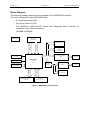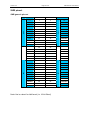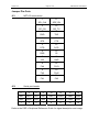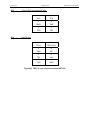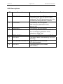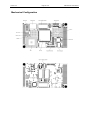
1
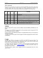
SMT363XC2
User Manual
User Manual (QCF42); Version 3.0, 8/11/00; © Sundance Multiprocessor Technology Ltd. 1999
Version 2.2
Page 2 of 27
SMT363XC2 User Manual
Revision History
Date
Comments
Engineer
Version
14/11/03
First release
JPA
1.0.0
02/12/03
Added addressing mode section (LED Setting)
JPA
1.0.1
JPA
1.0.2
Updated ComPort section
20/10/04
Updated block diagram.
Removed endianess section
Updated LED section
Replaced Timer and interrupt section by
Interrupt section
07/06/05
Added: power consumption
SM
1.0.3
09/08/05
Update: Support the firmware V1.1
SM
2.0
05/12/05
Updated LED descriptions.
GP
2.1
29/11/07
Removed HPI connection from block diagram.
GP
2.2
Version 2.2
Page 3 of 27
SMT363XC2 User Manual
Table of Contents
Revision History.......................................................................................................... 2
Table of Contents ....................................................................................................... 3
Contacting Sundance ................................................................................................. 5
Notational Conventions .............................................................................................. 6
DSP ........................................................................................................................ 6
SDB ........................................................................................................................ 6
SHB ........................................................................................................................ 6
Register Descriptions .............................................................................................. 6
Outline Description ..................................................................................................... 7
Intended Audience...................................................................................................... 7
Block Diagram ............................................................................................................ 8
Architecture Description ............................................................................................. 9
NET+50 ...................................................................................................................... 9
DSP ............................................................................................................................ 9
Boot Mode............................................................................................................... 9
DPRAM ................................................................................................................. 10
EMIF Control Registers......................................................................................... 10
CE1 - IO Control ................................................................................................... 11
SDRAM..................................................................................................................... 11
FLASH ...................................................................................................................... 11
RS232 ...................................................................................................................... 12
Serial ports ............................................................................................................... 12
FPGA........................................................................................................................ 12
Version control ...................................................................................................... 12
Firmware versions .................................................................................................... 12
Reprogramming the firmware and boot code............................................................ 12
Comports .................................................................................................................. 13
SHB .......................................................................................................................... 13
Architecture........................................................................................................... 13
Global bus ................................................................................................................ 13
Version 2.2
Page 4 of 27
SMT363XC2 User Manual
LED Setting .............................................................................................................. 14
LED Register......................................................................................................... 14
CONFIG & NMI......................................................................................................... 15
Config Register ..................................................................................................... 15
Timer ........................................................................................................................ 16
Timer Control Register .......................................................................................... 16
IIOF interrupt ............................................................................................................ 17
Code Composer ....................................................................................................... 18
Application Development .......................................................................................... 18
SMT6400 .............................................................................................................. 18
SMT6060 .............................................................................................................. 18
3L Diamond........................................................................................................... 18
SMT6500 .............................................................................................................. 18
FPGA Memory Map.................................................................................................. 19
SHB pinout ............................................................................................................... 20
SHB generic pin-out .............................................................................................. 20
Jumper Pin-Outs....................................................................................................... 21
JP1
- NET+50 connections ............................................................................ 21
JP2
- Serial port header ................................................................................. 21
JP3
- Xilinx CPLD programming port. ............................................................ 22
JP4
- NetICE port........................................................................................... 22
LED Descriptions...................................................................................................... 23
Mechanical Configuration ......................................................................................... 24
Operating Conditions................................................................................................ 25
Safety.................................................................................................................... 25
EMC ...................................................................................................................... 25
General Requirements .......................................................................................... 25
Power Consumption.............................................................................................. 25
Bibliography.............................................................................................................. 26
INDEX ...................................................................................................................... 27
Version 2.2
Page 5 of 27
SMT363XC2 User Manual
Contacting Sundance
You can contact Sundance for additional information by login onto the Sundance
support forum. Please note that first users have to register first.
Version 2.2
Page 6 of 27
SMT363XC2 User Manual
Notational Conventions
DSP
The terms DSP, C6713 and TMS320C6713 will be used interchangeably throughout
this document.
SDB
The term SDB will be used throughout this document to refer to the Sundance Digital
Bus interface.
SHB
The term SHB will be used throughout this document to refer to the Sundance Highspeed Bus interface.
Register Descriptions
The format of registers is described using diagrams of the following form:
31–24
23–16
15–8
7–0
R,00000000
R,10000000
OFLAGLEVEL
R,00000000
RW,10000000
The digits at the top of the diagram indicate bit positions within the register and the
central section names bits or bit fields. The bottom row describes what may be done
to the field and its value after reset. Shaded fields are reserved and should only ever
be written with zeroes.
R
Readable by the CPU
W
Writeable by the CPU
RW
Readable and writeable by the CPU
Binary digits indicate the value of the field after reset
Version 2.2
Page 7 of 27
SMT363XC2 User Manual
Outline Description
The SMT363XC2 is an Ethernet module, size 1 TIM offering the following features:
NetSilicon ARM-chip Net+50
TMS320C6713 processor running at 225MHz
Six Comports
64MB of SDRAM
8MB Flash ROM
Global Bus connector
High bandwidth data I/O via 2 Sundance Digital Buses (SDB)
Intended Audience
There are two existing versions of the firmware for the SMT363XC2. These two
versions differ by the number and the type of communication resources (comport and
SDB interfaces) provided.
For each of the versions of the different firmware is loaded in the FPGA:
-
Firmware version 1.0 or
-
Firmware version 1.1
This user manual covers the version 1.1 of the firmware for the SMT363XC2
implemented with the model described in the SMT6500 help file.
The changes between the firmware version 1.0 and version 1.1 are described in the
section Firmware versions.
Version 2.2
Page 8 of 27
SMT363XC2 User Manual
Block Diagram
The following drawing shows the block diagram of the SMT363XC2 module.
The main components of the SMT363XC2 are:
-
A Texas Instruments DSP
-
One Xilinx Virtex-II FPGA
-
One NetSilicon ARM Net+50 device with integrated MAC controller for
connection to an Ethernet network.
-
16/64MB of SDRAM
DSP and
FPGA PSU
J1 Top Primary TIM
Connector
Comm-Port 3
Timer,& Control
15 I/O pins
2x Comm-Ports/SDL
24 I/O pins
8M bytes Flash
4 LEDs &
4 I/O pins
16/64M bytes
SDRAM
2 x (4/16M x 16)
32-bit EMIF
'C6211/6711/6713
DSP
McBSP,
GPIO, LEDs
Xilinx FPGA
Virtex-II
JTAG Header
1.5V
Dual Port
RAM
J3 Global Expansion
Connector
4x Comm-Port/SDL
48 I/O pins
Global Bus
74 I/O pins
Sundance High-speed
Bus
60-way Samtec
J2 Bottom Primary TIM
Connector
Comm-Port 1, 2, 4
Figure 1: SMT363XC2 block diagram
NET+50
16M bytes SDRAM
2 x (4M x 16)
RJ45, RS232,
LEDs
Version 2.2
Page 9 of 27
SMT363XC2 User Manual
Architecture Description
NET+50
The NET+50 is a cost-effective, high-performance 32-bit network attached
microprocessor developed especially for high-bandwidth applications in Intelligent
Networked Devices. Based on ARM's architecture, it integrates 10/100Base-T
Ethernet MAC with an MII interface, a distributed 10-channel linking DMA controller
and a memory controller supporting all of the popular memory devices in use today.
This device is connected directly to an Intel LXT971 PHY device, which provides an
IEEE 802.3 compatible 10Base-T and 100Base-T physical layer interface.
Also, directly connected to the NET+50 are 16Mbytes of SDRAM, an RS232 level
converter and a 128KB Dual Port RAM (DPRAM).
LEDs 4 and 4 are controlled via PORTA bits 0 and 1.
DSP
The Texas Instruments DSP can run at up to 225MHz. The DSP is doted of 16MB
(optional 64MB) of SDRAM.
The DSP is a TMS320C6713 type.
An on-board 37.5MHz crystal oscillator provides the clock used for the DSP which
then multiplies this by for input to the DSP. DSP internally multiplies this up to the
required frequency, using a PLL.
Boot Mode
The DSP is connected to the on-board flash ROM that contains the Sundance
bootloader and the FPGA bitstream.
Following reset, the DSP will automatically load the data from the flash ROM into its
internal program memory at address 0 and then start executing from there. All this
code is the Sundance bootloader, and it is made up of three parts: FPGA
configuration, processor configuration and the Comport boot procedure. FPGA
configuration uses data in the ROM to configure the FPGA. A processor configuration
sets the processor into a standard state, copies its comport boot procedure into a
dual-port RAM (DPRAM) implemented in the FPGA, and releases the NET+50 chip
from reset. The Net+50 chip is configured to boot from this DPRAM.
The bootloader is executed. It will continually check the six comports until data
appears on one of them. This will next load a program in boot format from this
comport. Note that the bootloader will not read data arriving on other comports.
Finally the control is passed to the loaded DSP application.
It is safest to wait for the configuration to complete. Note that comports will appear to
be "not ready" until the FPGA has been configured.
The FPGA programming algorithm is not described here. It can be found in the boot
code.
Version 2.2
Page 10 of 27
SMT363XC2 User Manual
DPRAM
The DPRAM in the FPGA is only intended to be used during this boot process; more
general use is not recommended.
A 128KB memory is directly connected to both the DSP and the NET+50 devices.
Each can access the memory independently and at their respective maximum data
rates.
The DPRAM is decoded as the boot ROM in the NET+50’s memory space.
The DPRAM supports the generation of interrupts to either of its ports. This
functionality is achieved by the DSP writing to a specific DPRAM address, which in
turn generates an interrupt to the NET+50 (PINT2* pin). Similarly, the NET+50 can
write to a specific address which generates an interrupt which can be routed to the
DSP.
EMIF Control Registers
The DSP has a single external memory interface (EMIF) which is 32 bits wide.
A full description of the registers used to control the EMIF can be found in the DSP
C6000 Peripherals Reference GuideError! Reference source not found.Error!
Reference source not found..
The standard bootstrap will initialise these registers to use the following resources:
Memory space
Resource
Address range
CE0
SDRAM
0x80000000 - 0x83FFFFFF
CE1
Flash / IO Control
0x90000000 - 0x903FFFFF
CE2
DPRAM
0xA0000000 - 0xA7FFFFFF
CE3
Virtex
0xB0000000 - 0xB0FFFFFF
(EMIF)
The power on (and reset) state for the semaphore enable (DPRAM related) is
disabled. This bit determines whether the flash or DPRAM-semaphore registers are
accessed on CE1.
Version 2.2
Page 11 of 27
SMT363XC2 User Manual
CE1 - IO Control
Several I/O connections are required to control the NET+50 reset signal, upper flash
address signals, and the control signals for FPGA programming. These are all
accessed via the CE1 memory space and defined settings for some data lines.
D31
D30
D29
D0
Function
0
0
0
X
Flash write
0
0
1
N
NET+50 reset control. Reset(active low)=N
0
1
0
N
Flash address A20 control. A20=N
0
1
1
N
Flash address A21 control. A21=N
1
0
0
N
FPGA PROG pin control. PROG(active low)=N
1
0
1
X
FPGA CCLK pin control. Generates pulse on CCLK
1
1
0
N
DPRAM semaphore enable when N=1
SDRAM
Memory space CE0 is used to access 16MB (or optional 64MB) of SDRAM over the
EMIF.
The speed of the SDRAM is dependent on the processor variant. Using the C6713,
the SDRAM will operate at 100MHz.
Using the C6713, the SDRAM operates at a programmable rate up to the maximum
allowed on the EMIF.
The EMIF CE0 memory space control register should be programmed with the value
0x00000030.
FLASH
An 8MB Flash ROM is connected to the DSP in the EMIF CE1 memory space. The
ROM holds boot code for the DSP, configuration data for the FPGA, the boot code
for the Net+50 chip and optional user-defined code.
A software protection algorithm is in place to prevent programs accidentally altering
the ROM’s contents. Please contact Sundance for further information about reprogramming this device.
The CE1 memory space control register should be programmed with the value
0xFFFFFF23.
Version 2.2
Page 12 of 27
SMT363XC2 User Manual
RS232
A single RS-232 channel is provided at true RS232 levels. The signals provided are
TBD and are presented on wire-wrap posts.
Serial ports
The DSP provides two serial ports, which are connected to a pin header on the
SMT363XC2 module. Additionally, some of the serial port signals are connected to
the Virtex2 FPGA in order to provide extra signals, which can be used for external
interrupts.
FPGA
The FPGA (Field Programmable Gate Array) is a Xilinx Virtex-II XC2V1000 device.
It implements the following communication resources:
•
Six comport interfaces
•
Two 16-bit Sundance Digital Bus interfaces
•
One global bus interface
Version control
Revision numbers for both the boot code and FPGA firmware are stored in the Flash
ROM during programming as zero-terminated ASCII strings.
The SMT6001 utility can be used to display the version numbers of the bootloader
and the FPGA data.
Firmware versions
The SMT6001 utility includes the latest version of the bootloader and the latest
version of the FPGA data that implements the FPGA architecture described in the
SMT6500 help file.
Note that the new firmware supports two more comports. Customers who wish to use
the old firmware that supported only 4 comports options can obtain it from our
support web forum.
Reprogramming the firmware and boot code
The contents of the flash ROM are managed using the SMT6001 utility. This includes
the latest firmware and bootloader along with complete documentation on how to
reprogram the ROM. The utility assumes that you have Code Composer Studio
installed and that it has been configured correctly for the installed TIMs. The
Sundance Wizard can help you with this.
To confirm that the ROM has been programmed correctly, you should run the
confidence test in the BoardInfo utility (SMT6300).
Version 2.2
Page 13 of 27
SMT363XC2 User Manual
Comports
The DSP has 6 comports, numbered 0 to 5.
The addresses of the Comport registers are shown in the Error! Reference source
not found., and are described in the SMT6400 help file.
SHB
The SMT363XC2 provides one SHB connector, which is connected to the DSP to
give two 16-bit SDB interfaces. These interfaces operate with a fixed clock rate of
100MHz.
Architecture
SDB0 and SDB1 on the DSP are presented on the TIM's SHB connector, SDBA and
SDBB respectively.
SDBB
SDBA
The addresses of the SDB registers are shown in the Virtex Memory Map, and are
described in the SMT6400 help file.
Global bus
The SMT363XC2 provides a single global bus interface. This is only accessible from
the DSP. The addresses of the global bus registers are shown in the Virtex Memory
Map, and are described in the SMT6400 help file.
Version 2.2
Page 14 of 27
SMT363XC2 User Manual
LED Setting
The SMT363XC2 has 8 LEDs.
LED D1 always displays the state of the FPGA DONE pin. This LED is off when the
FPGA is configured (DONE=1) and on when it is not configured (DONE=0).
This LED should go on when the board is first powered up and go off when the FPGA
has been successfully programmed (this is the standard operation of the boot code
resident in the flash memory device). If the LED does not light at power-on, check
that you have the mounting pillars and screws fitted properly. If it stays on, the DSP
is not booting correctly, or is set to boot in a non-standard way.
Two of the LEDs (D2-3) can be controlled with the LED register. Writing 1 will
illuminate the LED; writing 0 will turn it off.
LED Register
(0xB00D0000)
31–4
3
2
1
0
-
-
LED
D3
LED
D2
RW,0
RW,1
RW,0
RW,0
Despite LED register bit 2 is writable; user should not change the value of this bit.
When SMT363XC2 embeds 16MB of SDRAM, the DSP is configured to access
SDRAM with 8 column address bits and 12 row address bits, whereas when
SMT363XC2 embeds 64MB SDRAM, it’s configured with 10 column address bits and
13 row address bits (EMIF SDRAM Control register).
It results that FPGA’s is moved in the DSP’s memory space.
Writing a value to this bit changes the way the FPGA decodes the address, and
therefore it's location in the EMIF memory space.
This bit should be set to ‘1’ when 64MB of SDRAM are fitted on-board; otherwise it
should be set to ‘0’ when 16MB of SDRAM are fitted on-board.
Version 2.2
Page 15 of 27
SMT363XC2 User Manual
CONFIG & NMI
The TIM specification describes the operation of an open-collector type signal
CONFIG that is driven low after reset.
This signal, on a standard C4x based TIM, is connected to the processor’s IIOF3 pin.
On the SMT365, the CONFIG signal is asserted after power on, and can be released
by writing the value (1<<6) to the config register. Conversely, CONFIG may be reasserted by writing 0 to this bit. It is not possible for software to read the state of the
CONFIG signal.
The NMI signal from the TIM connector can be routed to the DSP NMI pin.
WARNING: Several software components include code sequences that assume
setting GIE=0 in the DSP CSR will inhibit all interrupts; NMI violates that assumption.
If an NMI occurs during such code sequences it may not be safe to return from the
interrupt. This may be particularly significant if you are using the compiler’s software
pipelining facility.
Config Register
31–8
Field
CONFIG
NMI
7
6
NMI
CONFIG
Description
0
drive CONFIG low
1
tri-state CONFIG
0
Disconnect NMI from the DSP
1
Connect NMI from TIM to the DSP.
Config and NMI DSP lines are described in the SMT6400 help file.
5–0
Version 2.2
Page 16 of 27
SMT363XC2 User Manual
Timer
The TIM TCLK0 and TCLK1 signals can be routed to the DSP’s TOUT/TINP pins.
The signal direction must be specified, together with the routing information in the
timer control register.
Timer Control Register
Field
31–6
5
4
3–0
Reserved
TCLK1
TCLK0
Reserved
Description
TCLK0
TCLK1
0
TIM TCLK0 is an input
1
Enable TIM TCLK0 as an output
0
TIM TCLK1 is an input
1
Enable TIM TCLK1 as an output
If the TIM TCLKx pin is selected as an output, the DSP TOUTx signal will be used to
drive it. The TIM TCLKx pin will always drive the DSP TINPx input.
TCLK0EN
C6x
TOUT0
TINP0
TCLK0
FPGA
The Timer control register is described in the SMT6400 help file.
Version 2.2
Page 17 of 27
SMT363XC2 User Manual
IIOF interrupt
The firmware can generate pulses on the external interrupt lines of the TIM.
Only the interrupt line IIOF1 and IIOF2 are connected from/to the DSP and the
HOST.
•
IIOF1 is connected from the DSP side to the HOST side: so, the DSP
interrupts the HOST
•
IIOF2 is connected from the HOST side to the DSP side: so, the HOST
interrupts the DSP
The IIOF interrupt lines are described in the SMT6400 help file.
Version 2.2
Page 18 of 27
SMT363XC2 User Manual
Code Composer
This module is fully compatible with the Code Composer Studio debug and
development environment. This extends to both the software and JTAG debugging
hardware. The driver to use is the tixds6x1x_11.dvr. CCS version 3.0 or later is
required as the reprogramming utility (SMT6001) requires it.
Troubleshooting
Our Knowledge data base and FAQ sections may help you to resolve some known
issues.
Application Development
Depending on the complexity of your application, you can develop code for
SMT363XC2 modules in several ways.
SMT6400
For simple applications, the Sundance SMT6400 software support package (project
examples) and its associated header files (SmtTim.h and ModSup.h) can suffice.
The SMT6400 product is installed by the Sundance Wizard and it is free of charge.
SMT6060
SMT6060-FTP is a utility that allows and easy and cost-effective integration of the Net+50 ARM chip
and the DSP that can be found on SMT363. It is ready to use and provide a TCI/IP interface to a host.
SMT6060-TCPIP is a software package that provides Ethernet connectivity via the industry standard
Berkeley sockets interface to a 3L/Diamond network of DSP processors. The package is typically used
when there is at least one SMT363 present in the system; however, using a feature of the SMT6025
software package, it also provides seamless connectivity via the HOST PC’s (Winsock 2.2) Ethernet
hardware. The software is ready-to-use and provides sockets connectivity to any Sundance DSP
processor.
3L Diamond
This module is fully supported by 3L Diamond, which Sundance recommends for all
but the simplest of applications. An SMT363XC2 has to be declared as appropriate in
configuration files as one processors of type:
•
SMT363XC2_1 (16MB SDRAM)
•
SMT363XC2_2 (64MB SDRAM)
SMT6500
This is the support package for the FPGA. It may be used to develop your application
in the FPGA of the module.
Version 2.2
Page 19 of 27
SMT363XC2 User Manual
FPGA Memory Map
volatile unsigned *SMT363CP0
=(unsigned *)0xB0000000;
volatile unsigned *SMT363CP1
=(unsigned *)0xB0008000;
volatile unsigned *SMT363CP2
=(unsigned *)0xB0010000;
volatile unsigned *SMT363CP3
=(unsigned *)0xB0018000;
volatile unsigned *SMT363CP4
=(unsigned *)0xB0020000;
volatile unsigned *SMT363CP5
=(unsigned *)0xB0028000;
volatile unsigned *SMT363CP0_STAT
=(unsigned *)0xB0004000;
volatile unsigned *SMT363CP1_STAT
=(unsigned *)0xB000C000;
volatile unsigned *SMT363CP2_STAT
=(unsigned *)0xB0014000;
volatile unsigned *SMT363CP3_STAT
=(unsigned *)0xB001C000;
volatile unsigned *SMT363CP4_STAT
=(unsigned *)0xB0024000;
volatile unsigned *SMT363CP5_STAT
=(unsigned *)0xB002C000;
volatile unsigned *SMT363STAT
=(unsigned *)0xB003C000;
volatile unsigned *SMT363SDBA
=(unsigned *)0xB0040000;
volatile unsigned *SMT363SDBB
=(unsigned *)0xB0050000;
volatile unsigned *SMT363SDBA_STAT
=(unsigned *)0xB0048000;
volatile unsigned *SMT363SDBB_STAT
=(unsigned *)0xB0058000;
volatile unsigned *SMT363SDBA_FLAG
=(unsigned *)0xB004C000;
volatile unsigned *SMT363SDBB_FLAG
=(unsigned *)0xB005C000;
volatile unsigned *GLOBAL_BUS
=(unsigned *)0xB00A0000;
volatile unsigned *GLOBAL_BUS_CTRL
=(unsigned *)0xB0080000;
volatile unsigned *GLOBAL_BUS_START
=(unsigned *)0xB0088000;
volatile unsigned *GLOBAL_BUS_LENGTH
=(unsigned *)0xB0090000;
volatile unsigned *SMT363TCLK
=(unsigned *)0xB00C0000;
volatile unsigned *SMT363TIMCONFIG
=(unsigned *)0xB00C8000;
volatile unsigned *SMT363LED
=(unsigned *)0xB00D0000;
volatile unsigned *SMT363INTCTRL4
=(unsigned *)0xB00E0000;
volatile unsigned *SMT363INTCTRL4_EXT
=(unsigned *)0xB00E4000;
volatile unsigned *SMT363INTCTRL5
=(unsigned *)0xB00E8000;
volatile unsigned *SMT363INTCTRL4_EXT
=(unsigned *)0xB00Ec000;
volatile unsigned *SMT363INTCTRL6
=(unsigned *)0xB00F0000;
volatile unsigned *SMT363INTCTRL4_EXT
=(unsigned *)0xB00f4000;
volatile unsigned *SMT363INTCTRL7
=(unsigned *)0xB00F8000;
volatile unsigned *SMT363INTCTRL4_EXT
=(unsigned *)0xB00fc000;
Version 2.2
Page 20 of 27
SMT363XC2 User Manual
SHB pinout
SHB generic pin-out
QSH Pin number
CLK
1
2
D0
D1
3
4
D2
D3
5
6
D4
D5
7
8
D6
D7
9
10
D8
D9
11
12
D10
D11
13
14
D13
15
16
D14
D15
17
18
USERDEF0
USERDEF1
19
20
USERDEF2
USERDEF3
21
22
WEN
REQ
23
24
ACK
25
26
27
28
29
30
31
32
33
34
35
36
CLK
37
38
D0
D1
39
40
D2
D3
41
42
D4
D5
43
44
D6
D7
45
46
D8
D9
47
48
D10
D11
49
50
D13
51
52
D14
D15
53
54
USERDEF0
USERDEF1
55
56
USERDEF2
USERDEF3
57
58
WEN
REQ
59
60
ACK
Note: Hw is a short for Half-word (i.e. 16-bit Word)
Hw
Hw0
QSH Pin number
Hw1
Hw1
Hw0
Hw
D12
D12
Version 2.2
Page 21 of 27
SMT363XC2 User Manual
Jumper Pin-Outs
JP1
JP2
-
NET+50 connections
-
1
11
SPI_CLK
SPE_EN
2
12
SPI_RX
SPI_TX
3
13
RXD
TXD
4
14
RTS
CTS
5
15
DTR
DCD
6
16
DSR
RI
7
17
V33
GND
8
18
FA6
FA78
9
19
FA3
FA45
10
20
FA1
FA2
Serial port header
2
4
6
8
10
12
14
16
FSX1
FSR1
DX1
DR1
CLKX1
CLKR1
CLKS1
GND
FSX2
FSR2
DX2
DR2
CLKX2
CLKR2
CLKS2
GND
1
3
5
7
9
11
13
15
Refer to the DSP’s Peripheral Reference Guide for signal description and usage.
Version 2.2
JP3
JP4
-
-
Page 22 of 27
SMT363XC2 User Manual
Xilinx CPLD programming port.
1
2
V33
TCK
3
4
GND
TMS
5
6
TDO
TDI
1
2
TCLK
TRST (NC)
3
4
TMS
NC
5
6
TDI
V33
7
8
TDO
GND
NetICE port
Typically, TRST is not connected to the NET+50.
Version 2.2
Page 23 of 27
SMT363XC2 User Manual
LED Descriptions
LED
Connection
Function
1
FPGA.DONE
Shows the state of the FPGA’s configuration.
If this LED is ON, then the FPGA is NOT
configured. This LED should power up in the
ON state and extinguish after a second.
2
FPGA.LED0
Controlled by the LED register.
DSP Heartbeat (SMT6060-TCPIP,
rpcproxy.tsk)
3
FPGA.LED1
Controlled by the LED register.
4
NET50.PORTA0
Controlled by PORTA bit 0 of the NET+50.
Net+50 Heartbeat (SMT6060-TCPIP,
netsocksvr_v0p5p7.dat)
5
NET50.PORTA1
Controlled by PORTA bit 1 of the NET+50.
6
PHY.LED3
Link receive status (ON=receiving, OFF=not
receiving)
7
PHY.LED2/NET50.PORTC6
Link up status (ON=connected,
OFF=disconnected)
8
PHY.LED1
Link speed status (ON=100Mbit,
OFF=10Mbit)
Version 2.2
Mechanical Configuration
Page 24 of 27
SMT363XC2 User Manual
Version 2.2
Page 25 of 27
SMT363XC2 User Manual
Operating Conditions
Safety
The module presents no hazard to the user.
EMC
The module is designed to operate within an enclosed host system that provides
adequate EMC shielding. Operation within the EU EMC guidelines is only guaranteed
when the module is installed within an appropriate host system.
The module is protected from damage by fast voltage transients introduced along
output cables from outside the host system.
Short-circuiting any output to ground does not cause the host PC system to lock up
or reboot.
General Requirements
The module must be fixed to a TIM40-compliant carrier board.
The SMT363XC2 TIM is in a range of modules that must be supplied with a 3.3V
power source. In addition to the 5V supply specified in the TIM specification, these
new generation modules require an additional 3.3V supply to be presented on the
two diagonally-opposite TIM mounting holes. The lack of this 3.3V power supply
should not damage the module, although it will obviously be inoperable; prolonged
operation under these circumstances is not recommended.
The SMT363XC2 is compatible with all Sundance TIM carrier boards. It is a 5V
tolerant module, and as such, it may be used in mixed systems with older TIM
modules, carrier boards and I/O modules.
Use of the TIM on SMT327 (cPCI) motherboards may require a firmware upgrade. If
LED D6 on the SMT363XC2 remains illuminated once the TIM is plugged in and
powered up, the SMT327 needs the upgrade. The latest firmware is supplied with all
new boards shipped. Please contact Sundance directly if you have an older board
and need the upgrade.
The external ambient temperature must remain between 0°C and 40°C, and the
relative humidity must not exceed 95% (non-condensing).
Power Consumption
The power consumption of this TIM is dependent on the operating conditions in terms
of core activity and I/O activity. The SMT363XC2 module consumes about 3.18
Watts.
Bibliography
1. Sundance Help file
2. SMT6400 help file (DSP support package) and SMT6500 help file (FPGA support package)
3. SMT6060 user manual (Ethernet support package)
4. NET+50 Microprocessor
5. TMS320C6000 Peripherals Reference Guide (literature number SPRU190)
It describes common peripherals available on the TMS320C6000 digital signal processors. This
book includes information on the internal data and program memories, the external memory
interface (EMIF), the host port, multichannel-buffered serial ports, direct memory access (DMA),
clocking and phase-locked loop (PLL), and the power-down modes.
6. TIM-40 MODULE SPECIFICATION Including TMS320C44 Addendum
7. SDB Technical Specification
8. SHB Technical Specification
9. TMS320C4x User's Guide (literature number SPRU063)
It describes the C4x 32-bit floating-point processor, developed for digital signal processing as well
as parallel processing applications. Covered are its architecture, internal register structure,
instruction set, pipeline, specifications, and operation of its six DMA channels and six
communication ports. Software and hardware applications are included.
10. Xilinx Virtex-II datasheet
11. TMSC6713 datasheet
User Manual (QCF42); Version 3.0, 8/11/00; © Sundance Multiprocessor Technology Ltd. 1999
Version 2.2
Page 27 of 27
SMT363XC2 User Manual
INDEX
A
M
Application Development · 18
memory space (CE0 to CE3) · 10
B
N
Bibliography · 26
Notational Conventions · 6
C
O
Code Composer · 18
CONFIG & NMI · 15
Contacting Sundance · 5
Operating Conditions · 25
E
email address · 5
F
Firmware versions · 12
I
IIOF lines · 17
L
LEDs · 14
FPGA DONE pin · 14
LED register · 14
P
Power consumption · 25
R
Register Descriptions · 6
S
SDB · 13
SHB pinout · 20
SMT6400 · 18
SMT6500 · 18
T
Timer · 16
V
Version Control · 12