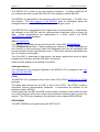
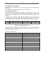
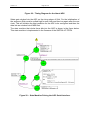
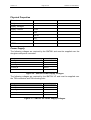
1
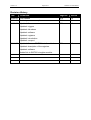
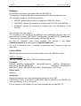
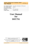
SMT391-VP
User Manual
Version 1.3
Page 2 of 41
SMT391-VP User Manual
Revision History
Date
Comments
Engineer
Version
25/04/05
First release
JPA
1.0
07/06/05
Added: power consumption
SM
1.1
16/08/05
Updated: firmware
JPA
1.2
JPA
1.3
Updated: triggers
Updated: ddr sdram
Updated: software
Updated: registers
Updated: introduction
Updated: comport
22/11/05
Updated: firmware/SMT391 interface block
Updated: description of the registers
Updated: software
Added link to SMT391 daughter module.
Version 1.3
Page 3 of 41
SMT391-VP User Manual
Table of Contents
Revision History.......................................................................................................... 2
Table of Contents ....................................................................................................... 3
Introduction................................................................................................................. 6
Overview ................................................................................................................. 6
Module Features ..................................................................................................... 6
Possible Applications .............................................................................................. 6
Related Documents ................................................................................................ 7
Hardware overview..................................................................................................... 8
Block diagram ......................................................................................................... 8
ADC AT84AD001B ................................................................................................. 9
Analogue features................................................................................................... 9
FPGA ...................................................................................................................... 9
DDR SDRAM .......................................................................................................... 9
SLB ....................................................................................................................... 10
SDB ...................................................................................................................... 10
RSL ....................................................................................................................... 10
Comport ................................................................................................................ 10
LED ....................................................................................................................... 10
External triggers.................................................................................................... 10
Clocks generation ................................................................................................. 11
Firmware................................................................................................................... 11
Block diagram ....................................................................................................... 11
SMT391 interface block ........................................................................................ 11
ADC data interface ............................................................................................ 12
ADC 3-wire interface ......................................................................................... 12
PLL - VCO (LMX2330U) interface ..................................................................... 12
Clock synthesiser (SY89430) interface.............................................................. 12
External clocks .................................................................................................. 12
Triggers ............................................................................................................. 12
Registers block ..................................................................................................... 14
SDB ...................................................................................................................... 14
Version 1.3
Page 4 of 41
SMT391-VP User Manual
RSL ....................................................................................................................... 14
Comport ................................................................................................................ 14
MPS430 block....................................................................................................... 14
Design Resource Usage ....................................................................................... 14
Software ................................................................................................................... 16
Library SMT391 .................................................................................................... 16
SMT391_Config() .............................................................................................. 16
SMT391_Adc_Init()............................................................................................ 17
Config_LMX2330U().......................................................................................... 17
Library LMX2330U ................................................................................................ 17
LMX2330U_Parameters().................................................................................. 17
Library SY89430V................................................................................................. 18
SY89430V_Parameters() .................................................................................. 18
Description of the registers ....................................................................................... 19
Accessing the registers ......................................................................................... 19
Memory map ......................................................................................................... 21
Register Descriptions ............................................................................................ 23
Reset Register................................................................................................... 23
Firmware Version Register (Read Add 0x000) .................................................. 24
Temperature Registers (Read Add 0x020, 0x021, 0x028, 0x029)..................... 24
Serial Number Registers (Read Add 0x022 - 0x025 and 0x02A - 0x02D) ......... 25
ADC Clock Source Registers (Write Add 0x801)............................................... 26
Clock Synthesizer Setup Register (Write Add 0x800) ....................................... 26
PLL Setup Registers (Write Add 0x802 – 0x809) .............................................. 27
ADC Setup Registers (Write Add 0x80B, 0x80C).............................................. 29
Trigger register (0x042) ..................................................................................... 29
Installation ................................................................................................................ 30
How to connect your SMT391 to your SMT338-VP? ............................................ 30
Configuring the FPGA ........................................................................................... 33
Appendix................................................................................................................... 33
PLL (LMX2330U) interface.................................................................................... 33
Clock synthesiser interface ................................................................................... 35
ADC interface........................................................................................................ 37
Version 1.3
Page 5 of 41
SMT391-VP User Manual
Physical Properties................................................................................................... 40
Power Supply........................................................................................................ 40
Power consumption .............................................................................................. 41
Module Dimensions .............................................................................................. 41
Version 1.3
Page 6 of 41
SMT391-VP User Manual
Introduction
Overview
The SMT391-VP is a single width TIM module. It is capable of sampling two analog
inputs at 1 GSPS with a resolution of 8 bits. An Atmel dual channel ADC
(AT84AD001) performs the analogue to digital conversion.
Digital data is output to a Xilinx Virtex-II Pro FPGA (XC2VP30-6 - FF896 package).
Data samples from the ADC are transferred onto the RocketIO Serial Links on the
module (RSL) for real time applications.
It is also possible to capture a frame of data and transfer it over the Sundance Highspeed Bus (SHB). This interface is compatible with a wide range of Sundance
processor and I/O modules.
Module Features
The main features of the SMT391-VP are listed underneath:
•
Dual channel ADC (Ideal for I & Q channel applications)
•
1GHz sampling frequency
•
8 Bit data resolution
•
128 Mbytes DDR SDRAM for sample captures1
•
Custom trigger inputs via external connectors
•
Two Standard Sundance Comports
•
Two SHB interfaces for easy interconnection to Sundance products (interfaces
for data sample and non-real-time processing)
•
RSL interface for data streaming applications
•
On-board MSP430 microprocessor
Possible Applications
The SMT391-VP can be used for the following applications (this non-exhaustive list
should be taken as an example):
1
•
Broadband cable modem head-end systems
•
3G Radio transceivers
•
High-data-rate point-to-point radios
•
Medical imaging systems
•
Spectrum analyzers
The memory is available on the board but isn’t supported by the firmware
Version 1.3
Page 7 of 41
SMT391-VP User Manual
Related Documents
[1] Sundance High-speed Bus (SHB) specifications – Sundance.
ftp://ftp2.sundance.com/Pub/documentation/pdffiles/SHB_Technical_Specification_v1_0.pdf
[2] RocketIO Serial Links (RSL) specifications – Sundance.
ftp://ftp2.sundance.com/Pub/documentation/pdffiles/RSL_Technical_Specification_v1_0.pdf
[3] TIM specifications.
ftp://ftp2.sundance.com/Pub/documentation/pdf-files/tim_spec_v1.01.pdf
[4] Sundance LVDS Bus (SLB) specifications – Sundance.
http://www.sundance.com/docs/SLB%20-%20Technical%20Specifications.pdf
[5] Virtex-II Pro FPGA datasheet - Xilinx.
http://direct.xilinx.com/bvdocs/publications/ds083.pdf
[6] Dual 8-bit ADC datasheet - Atmel.
http://www.atmel.com/dyn/resources/prod_documents/doc2153.pdf
[7] Comport specification – Texas Instruments.
http://focus.ti.com/lit/ug/spru63c.pdf
[8] SMT391 daughter module user manual.
Channel B
Signal
Conditioning
LVPECL
Trigger
Dist ribution
Channel B
Input
Connector
Trigger
Input
Connector
Notes:
Channel A
Signal
Conditioning
Channel A
Input
Connector
Vin B
(1d)
Vin A
(1d)
Debug IOs
and LEDs
Dual 8Bit
1GSPS ADC
AT84AD001-A
Clock (2d)
The numbers in brackes denote
the amount of FPGA IO pins
requires. 'd' is used for differential
pairs. 1d Will thus requre 2 IOs
Power
LVPECL
Clock
Generation and
Dist ribution
Clock
Input
Connector
Low Jitter
Local Oscillator
Dat a (21)
Control (4)
Trigger (1d)
512MBit for
Channel B
ChB Data, Clock
and Control (18d)
ChA Data, Clock
and Control (18d)
Clock (1d)
Control (4)
Control (6)
512MBit for
Channel A
256MBit
DDR SDRAM
256MBit
DDR SDRAM
Data, Clock and
Control (93)
256MBit
DDR SDRAM
508 / 556 IOs
FF896 Package
Virtex-II Pro
XC2VP30
Data, Clock and
Control (93)
256MBit
DDR SDRAM
ChB Dat a, Clock
and Control (60)
DataTx (4d)
DataRx (4d)
ComPorts and
Control (59)
DataTx (4d)
DataRx (4d)
ChA Dat a, Clock
and Control (60)
SHB for Channel B
4 RocketIO
Links for Channel A
(1GByte/s effective
Data throughput)
Top and Bott om TIM
Connect ors
4 RocketIO
Links for Channel A
(1GByte/s effective
Data throughput)
SHB for Channel A
Version 1.3
Page 8 of 41
SMT391-VP User Manual
Hardware overview
Block diagram
The following diagram represents the architecture of the SMT391-VP module.
Version 1.3
Page 9 of 41
SMT391-VP User Manual
The SMT391-VP is made of two sub-modules combined. To make a SMT391-VP
you combine the base module SMT338-VP to the daughter module SMT391.
The SMT391 is responsible for the analogue side of the functionality. The ADC is on
this module. The user manual of the SMT391 gives all information about the
analogue features of the SMT391 (performances, analogue inputs, …)
The SMT338-VP is responsible for the digital side of the functionality. It implements
the interface to the SMT391 and the communication interfaces used to output the
data. These functionalities are implemented in a Xilinx Virtex-II Pro FPGA
(XC2VP30-6 in FF896 package).
ADC AT84AD001B
The SMT391-VP is based on the Atmel dual 8-bit 1 Gsps ADC AT84AD001B .
The AT84AD001B provides 1 Gsps sampling per channel or 2 Gsps sampling from
one channel (in the interleaving mode) and integrates dual on-chip track/holds that
provide excellent dynamic performance over 1.5 GHz input frequency bandwidth with
low 1.4 W power consumption.
This Dual ADC is dedicated to high speed, low power applications such as digital
sampling oscilloscopes and direct RF down-conversion.
Refer to Atmel website for the details of this ADC.
Analogue features
The description of the analogue features of the SMT391-VP is available in the user
manual of the SMT391.
FPGA
The SMT391-VP is populated with a Xilinx Virtex-II Pro FPGA (XC2VP30-6 in FF896
package).
The digital data coming from the ADC is sent to the FPGA. The FPGA is used to
implement various communication interfaces. It implements the interface to the
daughter module SMT391.
It also implements the RSL and SDB communication interfaces used to send the data
out of the module as well as the comport communication interface used to control the
module. The FPGA also implement the interface to the on-board DDR SDRAM.
DDR SDRAM
The DDR SDRAM is not supported by the SMT391-VP.
Version 1.3
Page 10 of 41
SMT391-VP User Manual
SLB
The SMT391-VP is composed of the SMT391 module plugged on the base module
SMT338-VP. Both modules communicate via the SLB.
SDB
The SMT391-VP comes with two SHB connectors. A 32-bits SDB interface is
mapped on each of the SHB to output the data stored in the DDR SDRAM.
RSL
The SMT391-VP comes with 8 RSL that can carry the data stream coming from the
ADC at up to 1GB/s. RSL are used for real time applications.
Refer to RSL specification for a complete description.
Comport
The SMT391-VP provides two comports: comport 0 and comport 3. The comport 3 is
used to control the module.
The FPGA is configured at power-up over Comport 3. The configuration process is
controlled by a microprocessor (a Texas Instruments MSP430 family microprocessor)
which shared the comport with the FPGA. Once the FPGA is configured the
configuration Comport is used for configuring control registers in the FPGA to control
the functions of the FPGA.
LED
Refer to the SMT338-VP user guide for the description of the LEDs.
External triggers
Two external triggers are available with the SMT391-VP. They are used to start the
acquisition of the analogue signal.
The external trigger input is received by a LVPECL input buffer on the SMT391. The
buffered signal is passed down as a differential LVPECL to the FPGA on the
SMT338-VP. For compatibility reasons with other daughter card modules there are
no ECL termination resistors mounted on the SMT338-VP. For this reason the pulse
width of the input trigger must be at least 1uS before the FPGA will register it.
As this might be a problem for some applications this issue has been resolved on the
newer SMT338-VP modules and appropriate termination resistors are provided to
improve the response time of the FPGA to an external trigger.
For most systems it is likely that there will be a system host (DSP Module). For this
reason it is also possible to send a software trigger to the SMT391-VP over Comport
3. There will however be latency from the time that the command is sent to the time
that data are acquired.
Version 1.3
Page 11 of 41
SMT391-VP User Manual
Clocks generation
The sampling clock of the ADC can be generated by an on-board VCO or an onboard clock synthesiser. Inputs for external clocks are available on the board but not
supported by the FPGA design.
Refer to the SMT391 user manual for further information.
Firmware
Block diagram
The following diagram represents the internal architecture of the FPGA of the
SMT391-VP.
Buffer
64 bits
SMT391
interface
block
SDB
RSL
64 bits
RSL
Buffer
SDB
Registers
Comport
SMT391 interface block
The following diagram shows the various blocks constituting the SMT391 block.
The SMT391 interface block implements the interface to the SMT391 daughter
module.
It receives the 1Gsps data stream coming from the ADC and provides it to the rest of
the design.
The data sampled by the ADC are output by this block, 8 samples at a time (64 bits)
at a 1/8 of the sampling clock of the ADC.
The firmware of the SMT391-VP supports one clock input for the ADC.
The ADC must be configured using the following clock selection mode:
-
CLKI Æ ADCI
Version 1.3
-
Page 12 of 41
SMT391-VP User Manual
CLKI Æ ADCQ
Any other configuration isn’t supported by the SMT391-VP. For example the
interlacing mode of the ADC is not supported by the default firmware of the
SMT391-VP.
The SMT391 block also includes the 3-wires interface used to configure the ADC as
well as the interfaces used to configure the clocks of the SMT391 daughter module.
Refer to the SMT391 user manual for more information about the clocks generation
feature of the SMT391-VP module.
ADC data interface
Support for a sub-set of the command controllable features of the Atmel ADC is
implemented in the firmware of the SMT391-VP. The ADC should be configured as
follow:
•
Data Demux 1:2 mode
•
Output Clock Fs/4
ADC 3-wire interface
The settings stored in the register block of the SMT391-VP are sent to the ADC via
this interface.
Refer to the appendix for more information about this interface.
PLL - VCO (LMX2330U) interface
A three wire uni-directional control interface is implemented between the FPGA and
the PLL on the daughter card. This PLL sets and controls the voltage for the VCO
that generates the main clock.
Refer to the LMX2330U user guide for the detailed description of the PLL.
Clock synthesiser (SY89430) interface
A three wire uni-directional controls interface is implemented between the FPGA and
the Micrel clock synthesizer on the daughter card. The clock synthesizer can
generate a variable 50 – 950 MHz clock. The jitter on this clock is higher than on the
main PLL+VCO clock, but it is convenient for testing.
External clocks
The external clocks are not supported by the SMT391-VP.
Triggers
There are two main sources for the trigger. The first is an LVPECL trigger received
over the MMBX connector. The second is a trigger command. The trigger command
is received over the Comport interface.
Version 1.3
Page 13 of 41
SMT391-VP User Manual
When the SMT391-VP receives a trigger, the SMT391 interface block gets activated
and starts capturing the samples sent by the ADC.
Connector J9 should be used to externally trigger the acquisition of both channels I
and Q.
Connector J10 should be left unconnected.
The following diagram is a graphical representation of the trigger structure and
sources on the SMT391-VP:
External Trigger
FPGA
External Trigger Input
(MMBX)
ComPort Interface
ComPort Rx Cmd
State Machine
LVPECL
Buffer
Trigger Generation
Trigger
Distribution
Trigger Setup
Register
Figure 1 – Module Trigger Structure.
Version 1.3
Page 14 of 41
SMT391-VP User Manual
Registers block
This block implements the registers of the SMT391-VP. The complete description of
the registers is available in the section “Description of the registers”. The registers
are updated via the comport 3 of the SMT391-VP.
The register block can not be reset to its default value. User must set each individual
register to the requested value.
SDB
The SMT391-VP implements two 32-bits SDB interfaces. Refer to the SMT6500 for
the complete description of the SDB.
The SDBs are clocked at 62.5 Mhz.
RSL
The SMT391-VP implements two groups of four RSL. There is one group of four
RSL per ADC channel.
The RSL makes used by default of a 10/8 encoding style which allow a data rate of
125 MB/sec per RSL. The main part of the data sent on the RSL is the ADC data.
However some control command is also part of the data stream, reducing slightly the
data rate below 1 GB/sec.
Comport
The SMT391-VP implements one comport interface.
Only the comport 3 is implemented.
Refer to the SMT6500 for the complete description of the comport.
MPS430 block
The SMT391-VP implements the interface to the micro-controller MPS430. The
FPGA can receive information such as the temperature of the ADC via this interface.
Design Resource Usage
The following table is a summary of the FPGA resources used by the demo design
that comes with the SMT391-VP (compiled for a VP30 device).
Resource
Number of External DIFFMs
Utilization
37 out of 276
Percentage
13%
Number of External DIFFSs
37 out of 276
13%
Number of External IOBs
244 out of 556
47%
244 out of 244
100%
Number of LOCed External IOBs
Version 1.3
Page 15 of 41
SMT391-VP User Manual
Number of RAMB16s
14 out of 136
10%
Number of SLICEs
4169 out of 13696
30%
Number of BUFGMUXs
10 out of 16
62%
Number of DCMs
4 out of 8
50%
Figure 2 – Virtex-II Pro Device Utilization Summary (non contractual values).
Version 1.3
Page 16 of 41
SMT391-VP User Manual
Software
An example is provided to get started with the SMT391-VP.
The example configures the module and generates files with the data acquired.
The example is based on the following libraries:
•
SMT391: gathers the functions to configure the SMT391 module
•
LMX2330U: gathers the functions to configure the PLL/VCO of the SMT391.
•
SY89430V: gathers the functions to configure the clock synthesiser of the
SMT391.
All the libraries are stand alone.
The functions of the smt391.lib, lmx2330U.lib and sy89430v.lib libraries take as a
parameter two functions SMT338VP_WriteRegister and SMT338VP_ReadRegister.
These functions are used to communicate with the SMT391-VP.
For the 3L Diamond users these functions are defined
DspDiamondLib.h and implemented in DspDiamondLib.lib.
in
the
library
For non 3L Diamond user, it possible to generate these functions using the
SMT6400.
Library SMT391
SMT391.lib gives access to the functions used to set up the SMT391 module.
SMT391_Config()
SMT391_Config configures the SMT391 daughter module.
Prototype
UINT32 SMT391_Config(UINT32 SamplingFrequency, UINT32 ClockSource,
SMT338VP_WRITE_REGISTER
SMT338VP_WriteRegister,
SMT338VP_READ_REGISTER SMT338VP_ReadRegister, UINT32 cp);
Return value
Always 0.
Parameters
SamplingFrequency: the requested sampling frequency of the ADC.
ClockSource: select if the source of the ADC clock is internal to the SMT391-VP
(clock synthesiser or PLL) or external.
Cp: the number of the comport to use to communicate with the SMT391-VP.
Version 1.3
Page 17 of 41
SMT391-VP User Manual
SMT391_Adc_Init()
SMT391_Adc_Init configure the ADC’s internal registers.
Prototype
void SMT391_Adc_Init(AT84AD001B_reg
SMT338VP_WriteRegister,
SMT338VP_ReadRegister,UINT32 cp);
r,
SMT338VP_WRITE_REGISTER
SMT338VP_READ_REGISTER
Return value
None.
Parameters
R: this structure reproduces the internal registers of the ADC. Refer to the data
sheet of the ADC for the description of the internal registers.
Cp: the number of the comport to use to communicate with the SMT391-VP.
Config_LMX2330U()
This function configures the LMX2330U.
Prototype
void Config_LMX2330U(UINT32 if_r, UINT32 if_n, UINT32 rf_r, UINT32 rf_n, UINT32
cp);
Return value
None.
Parameters
If_r, if_n, rf_r, rf_n: the values being written in the registers of the LMX2330U.
These values can be obtained using the function LMX2330U_Parameters().
Cp: the number of the comport to use to communicate with the SMT391-VP.
Library LMX2330U
LMX2330U_Parameters()
This function generates the value to program in the registers of the LMX2330U PLLVCO to generate the specified frequency.
Prototype
unsigned int LMX2330U_Parameters (unsigned int rf_frequency, unsigned int
if_frequency, unsigned int *if_r, unsigned int *if_n, unsigned int *rf_r, unsigned int
*rf_n);
Return value
0 always.
Parameters
Version 1.3
Page 18 of 41
Rf_Frequency: the frequency of the RF part of the PLL.
frequency of the ADC.
SMT391-VP User Manual
This is the sampling
If_Frequency: the frequency of the IF part of the PLL. This parameter must be zero.
*if_r, *if_n, *rf_r, *rf_n: the calculated values are returned into these variables. Refer
to the LMX2330U user guide for the details of the registers.
Library SY89430V
SY89430V_Parameters()
This function generated the parameters to use to configure the SY89430V
component for the requested frequency.
Prototype
unsigned int SY89430V_Parameters (unsigned int frequency);
Return value
The value to use the configure the SY89430V for the specified frequency. The value
returned should be written in the clock synthesiser setup register
(SMT391_ADJ_CLK_CNTRL_REG).
Parameters
Frequency: the requested frequency.
Version 1.3
Page 19 of 41
SMT391-VP User Manual
Description of the registers
The registers in the SMT391-VP firmware control the complete functionality of the
SMT391-VP.
These registers are configured via the comport 3 of the module.
Accessing the registers
It is possible to read and to write the registers of the SMT391-VP. When a write
access occurs the received data is stored into the selected register. When a read
access occurs, the SMT391-VP sends the content of the selected register to the
comport 3.
The data sent to the comport 3 of the SMT391-VP follows a certain format used to
specify the type of access requested and the address of the access. The data is mad
of a command, an address and a data. The following figure describes this format:
31 .. 28
Command
27 .. 24
23 .. 20
19 .. 16
15 .. 12
Address
11 .. 8
7 .. 4
Data MSB
3 .. 0
Data LSB
Figure 3 – Setup Packet Structure.
All maximum size of registers that can be written to or read is 16 Bits. When
performing a read bits 31 downto 16 will reflect the command and address. The lower
16 bits will contain the actual data.
The defined commands are:
Command Value
Command Description
0x0
Reserved
0x1
FGPA Write
0x2
FPGA Read
0x3
Reserved
0x4
Reserved
0x5
Reserved
0x6
Reserved
0x7
Reserved
0x8
Reserved
0x9
Reserved
0xA
Reserved
0xB
Reserved
0xC
Reserved
0xD
Reserved
0xE
Reserved
Version 1.3
0xF
Page 20 of 41
SMT391-VP User Manual
Reserved
Figure 4 – Packet Structure – Defined Commands.
Example 1:
Sending 0x1001FFFF over Comport3 from the Host to the SMT391-VP will Write, to
Address 0x001, Data FFFF
Example 2:
Sending 0x2801xxxx over Comport3 from the Host to the SMT391-VP will request a
Read, from Address 0x801. Once this command is received by the SMT391-VP, the
requested data will automatically be transmitted back over Comport 3, following the
same packet structure.
Version 1.3
Page 21 of 41
SMT391-VP User Manual
Memory map
The write packets must contain the address where the data must be written to and
the read packets must contain the address where the required data must be read.
The following figure shows the memory map for the writable and readable Control
Registers on the SMT391-VP:
Write Side
Address
Register
Read Side
Address
Register
0x000
Reserved
0x000
FirmwareVersion
0x001
ComInScratchReg0
0x001
ComOutScratchReg0
0x002
ComInScratchReg1
0x002
ComOutScratchReg1
0x003
Reserved
0x003
Reserved
0x004
Reserved
0x004
Reserved
0x005
Reserved
0x005
Reserved
0x006
Reserved
0x006
Reserved
0x007
Reserved
0x007
Reserved
0x008
Reserved
0x008
Reserved
0x009
Reserved
0x009
Reserved
0x00A
Reserved
0x00A
Reserved
0x00B
Reserved
0x00B
Reserved
0x00C
Reserved
0x00C
Reserved
0x00D
Reserved
0x00D
Reserved
0x00E
DdrACPCntrlReg
0x00E
DdrACPStatusReg
0x00F
DdrBCPCntrlReg
0x00F
DdrBCPStatusReg
0x010
Reserved
0x010
Reserved
0x011
Reserved
0x011
Reserved
0x012
Reserved
0x012
Reserved
0x013
Reserved
0x013
Reserved
0x014
DdrACPData0In
0x014
DdrACPData0Out
0x015
DdrACPData1In
0x015
DdrACPData1Out
0x016
DdrACPData2In
0x016
DdrACPData2Out
0x017
DdrACPData3In *
0x017
DdrACPData3Out +
0x018
DdrBCPCommand0In
0x018
Reserved
0x019
DdrBCPCommand1In
0x019
Reserved
0x01A
DdrBCPCommand2In
0x01A
Reserved
0x01B
DdrBCPCommand3In *
0x01B
Reserved
0x01C
DdrBCPData0In
0x01C
DdrBCPData0Out
0x01D
DdrBCPData1In
0x01D
DdrBCPData1Out
0x01E
DdrBCPData2In
0x01E
DdrBCPData2Out
0x01F
DdrBCPData3In *
0x01F
DdrBCPData3Out +
0x020
Reserved
0x020
Smt338AirTempReg
0x021
Reserved
0x021
Smt338DiodeTempReg
Version 1.3
Page 22 of 41
SMT391-VP User Manual
0x022
Reserved
0x022
Smt338SerialNoA
0x023
Reserved
0x023
Smt338SerialNoB
0x024
Reserved
0x024
Smt338SerialNoC
0x025
Reserved
0x025
Smt338SerialNoD
0x026
Reserved
0x026
Reserved
0x027
Reserved
0x027
Reserved
0x028
Reserved
0x028
DaughterCardAirTempReg
0x029
Reserved
0x029
DaughterCardDiodeTempReg
0x02A
Reserved
0x02A
DaughterCardSerialNoA
0x02B
Reserved
0x02B
DaughterCardSerialNoB
0x02C
Reserved
0x02C
DaughterCardSerialNoC
0x02D
Reserved
0x02D
DaughterCardSerialNoD
0x02E
Reserved
0x02E
Reserved
0x02F
Reserved
0x02F
Reserved
0x030
AdcDataCaptureCntrl
0x030
Reserved
0x031
Reserved
0x031
AdcADataOut (Fifo, will auto Rd Next after
a read)
0x032
Reserved
0x032
AdcBDataOut (Fifo, will auto Rd Next after
a read)
0x033
AdcResetReg
0x033
Reserved
0x034
AdcModeReg
0x034
Reserved
0x035
Reserved
0x035
Reserved
0x036
Reserved
0x036
Reserved
0x037
Reserved
0x038
Reserved
0x039
Reserved
0x03A
Reserved
0x03B
Reserved
0x03C
Reserved
0x03D
Reserved
0x03E
Reserved
0x03F
Reserved
0x040
Reserved
0x041
Reserved
0x042
TriggerReg
ADC Module Specific
ADC Module Specific
0x800
Smt391AdjClkCntrlReg *
0x800
Reserved
0x801
Smt391ClockSourceSelect
0x801
Reserved
0x802
Smt391Pll_IfR_Reg1
0x802
Reserved
0x803
Smt391Pll_IfR_Reg2
0x803
Reserved
0x804
Smt391Pll_IfN_Reg1
0x804
Reserved
Version 1.3
Page 23 of 41
SMT391-VP User Manual
0x805
Smt391Pll_IfN_Reg2
0x805
Reserved
0x806
Smt391Pll_RfR_Reg1
0x806
Reserved
0x807
Smt391Pll_RfR_Reg2
0x807
Reserved
0x808
Smt391Pll_RfN_Reg1
0x808
Reserved
0x809
Smt391Pll_RfN_Reg2 *
0x809
Reserved
0x80A
Smt391AdcCntrlReg
0x80A
Reserved
0x80B
Smt391AdcCntrlAddress
0x80B
Reserved
0x80C
Smt391AdcCntrlData *
0x80C
Reserved
0x80D
Reserved
0x80D
Reserved
0x80E
Reserved
0x80E
Reserved
0x80F
Reserved
0x80F
Reserved
* Write Data Valid pulse is generated when this register is written to.
+ A pre-read is generated on the first read. A second read is required to read the real
data.
Figure 5 – Register Memory Map.
For registers larger than 16 bits with an LSB and MSB part always write the LSB part
first and then the MSB.
Register Descriptions
Reset Register
The reset register is used to reset the various blocks constituting the FPGA.
Writing a ‘1’ will put the selected block in the reset state. Writing a ‘0’ will release the
reset.
15 .. 9
8 .. 0
Command
31 .. 28
27 .. 24
23 .. 20
Address
19 .. 16
Data MSB
Data LSB
1
0x000
Reserved
Reset command
Figure 6 – Reset Register (Write Only).
Reset command:
Bit 0: global reset of the FPGA. Reset all the logic in the FPGA except the comport
and the register block.
Bit 1: ADC interface channel Q reset (do not use).
Bit 2: ADC interface channel I reset.
Bit 3: SDB A reset.
Version 1.3
Page 24 of 41
SMT391-VP User Manual
Bit 4: SDB B reset.
Bit 5: RSL A reset.
Bit 6: RSL B reset.
Bit 7: Trigger logic reset channel Q (do not use).
Bit 8: Trigger logic reset channel I.
Firmware Version Register (Read Add 0x000)
A read from address 0x000 will display the firmware version register. The value of
this register is hard coded during VHDL compiles and must be stepped for each new
version of the firmware. Even though 32 bits are read over the Comport, the firmware
version register is a 16 bit register (16 least significant bits of the returned value).
Read Request Format:
31 .. 28
27 .. 24
23 .. 20
19 .. 16
15 .. 12
11 .. 8
7 .. 4
3 .. 0
Command
Address
Data MSB
Data LSB
0x2
0x000
xx
xx
Read Response Format:
31 .. 28
27 .. 24
23 .. 20
19 .. 16
15 .. 12
11 .. 8
7 .. 4
3 .. 0
Command
Address
Data MSB
Data LSB
0x2
0x000
Firmware Version
Firmware Version
Figure 7 – Firmware Version Register (Read Only).
Temperature Registers (Read Add 0x020, 0x021, 0x028, 0x029)
There are four temperature registers. Each register is 16 bits long. When the bit
value of the register is converted to a decimal number, that number is the
temperature in degrees Celsius.
Read Request Format:
31 .. 28
27 .. 24
Command
23 .. 20
19 .. 16
15 .. 12
11 .. 8
7 .. 4
3 .. 0
Address
Data MSB
Data LSB
0x2
0x020 (Smt338AirTempReg) (1)
xx
xx
0x2
0x021 (Smt338DiodeTempReg) (2)
xx
xx
0x2
0x028 (DaughterCardAirTempReg) (3)
xx
xx
0x2
0x029 (DaughterCardDiodeTempReg) (4)
xx
xx
(1)
- SMT338-VP Air Temperature on Top of PCB
Version 1.3
Page 25 of 41
SMT391-VP User Manual
(2)
– SMT338-VP FPGA temperature on Bottom of PCB
(3)
– SMT391 Air Temperature on Bottom of PCB
(4)
– SMT391 ADC temperature on Top of PCB (Not implemented)
Read Response Format:
31 .. 28
27 .. 24
23 .. 20
19 .. 16
15 .. 12
11 .. 8
7 .. 4
3 .. 0
Command
Address
Data MSB
Data LSB
0x2
0x020
SMT338-VP
Air Temperature
0x2
0x021
SMT338-VP
Diode Temperature
0x2
0x028
SMT391
Air Temperature
0x2
0x029
SMT391
Diode Temperature
Figure 8 – Temperature Registers (Read Only).
Serial Number Registers (Read Add 0x022 - 0x025 and 0x02A - 0x02D)
There is a unique silicon serial number IC on both the SMT338-VP and the SMT391.
Each serial number is 64 bits long and is thus requires four 16 bit registers to store
the value.
Read Request Format:
31 .. 28
27 .. 24
23 .. 20
19 .. 16
15 .. 12
11 .. 8
7 .. 4
3 .. 0
Command
Address
Data MSB
Data LSB
0x2
0x022 (Smt338SerialNoA)
xx
xx
0x2
0x023 (Smt338SerialNoB)
xx
xx
0x2
0x024 (Smt338SerialNoC)
xx
xx
0x2
0x025 (Smt338SerialNoD)
xx
xx
0x2
0x02A (DaughterCardSerialNoA)
xx
xx
0x2
0x02B (DaughterCardSerialNoB)
xx
xx
0x2
0x02C (DaughterCardSerialNoC)
xx
xx
0x2
0x02D (DaughterCardSerialNoD)
xx
xx
Figure 9 – Serial Number Registers (Read Only).
Read Response Format:
31 .. 28
Command
27 .. 24
23 .. 20
Address
19 .. 16
15 .. 12
Data MSB
11 .. 8
7 .. 4
3 .. 0
Data LSB
Version 1.3
Page 26 of 41
SMT391-VP User Manual
0x2
0x022
SMT338-VP Serial No
Byte A
0x2
0x023
SMT338-VP Serial No
Byte B
0x2
0x024
SMT338-VP Serial No
Byte C
0x2
0x025
SMT338-VP Serial No
Byte D
0x2
0x02A
SMT391 Serial No
Byte A
0x2
0x02B
SMT391 Serial No
Byte B
0x2
0x02C
SMT391 Serial No
Byte C
0x2
0x02D
SMT391 Serial No
Byte D
Figure 10 – Serial Number Registers Cont. (Read Only).
ADC Clock Source Registers (Write Add 0x801)
The ADC can receive a clock from the on-board VCO or the on-board clock
synthesizer. The following table shows the different combinations for setting up the
SMT391 clock tree.
Register
Value
ADC Clock Source
0x0000
On-board VCO
0x0001
On-board Clock Synthesizer
Figure 11 – Clock Source Selection Table (Write Only).
31 .. 28
27 .. 24
23 .. 20
19 .. 16
15 .. 12
11 .. 8
7 .. 4
3 .. 0
Command
Address
Data MSB
Data LSB
0x1
0x801
0x00
Clock Register Value
Figure 12 – Clock Source Register (Write Only).
Clock Synthesizer Setup Register (Write Add 0x800)
This register sets up the frequency of the clock synthesizer on the SMT391. Any write
operation to this register will trigger the clock synthesizer interface control logic to
initialize the clock synthesizer with its new value.
31 .. 28
27 .. 24
23 .. 20
19 .. 16
15 .. 12
11 .. 8
7 .. 4
3 .. 0
Version 1.3
Page 27 of 41
SMT391-VP User Manual
Command
Address
Data MSB
Data LSB
0x1
0x800
Data
Data
Figure 13 – Clock Synthesizer Setup Register (Write Only).
The data is arranged as follow:
Clock Control Register
Byte
1
Bit 7
Bit 6
Bit 5
Do Not Care
Bit 4
Bit 3
Bit 2
Test Bits
0
Bit 1
Output Division
Bit 0
M Count
M Count
Refer to the appendix for more details.
PLL Setup Registers (Write Add 0x802 – 0x809)
These registers set up the frequency of the PLL circuit on the SMT391. There are
two sets of registers – one set for setting up the IF side of the PLL, and the other set
for setting up the RF side of the PLL. The IF side is connected to a 200 – 350 MHz
VCO circuit and the RF side is connected to a 600 – 1000 MHz VCO circuit. All
registers must be initialized, and only when writing to the final register will both the IF
and RF side be configured to their new values.
31 .. 28
27 .. 24
23 .. 20
19 .. 16
15 .. 12
11 .. 8
7 .. 4
Data MSB
3 .. 0
Command
Address
Data LSB
0x1
0x802
Smt391Pll_IfR_Reg1
Smt391Pll_IfR_Reg1
0x1
0x803
Smt391Pll_IfR_Reg2
Smt391Pll_IfR_Reg2
0x1
0x804
Smt391Pll_IfN_Reg1
Smt391Pll_IfN_Reg1
0x1
0x805
Smt391Pll_IfN_Reg2
Smt391Pll_IfN_Reg2
0x1
0x806
Smt391Pll_RfR_Reg1
Smt391Pll_RfR_Reg1
0x1
0x807
Smt391Pll_RfR_Reg2
Smt391Pll_RfR_Reg2
0x1
0x808
Smt391Pll_RfN_Reg1
Smt391Pll_RfN_Reg1
0x1
0x809
Smt391Pll_RfN_Reg2
Smt391Pll_RfN_Reg2
Figure 14 – PLL Setup Registers (Write Only).
The data in the registers is arranged as follow:
Smt391Pll_IfR_Reg1 - Smt391Pll_RfR_Reg1
Byte
1
0
Bit 7
Bit 6
Bit 5
Bit 4
Bit 3
R_CNTRL (5 .. 0)
R_CNTRL (13 .. 6)
Bit 2
Bit 1
Bit 0
Address field
Version 1.3
Page 28 of 41
SMT391-VP User Manual
Smt391Pll_IfR_Reg2 - Smt391Pll_RfR_Reg2
Byte
Bit 7
Bit 6
Bit 5
Bit 4
Bit 3
Bit 2
Bit 1
Bit 0
1
Reserved
Reserved
FoLD0
FoLD2
TRI_STATE
IDo
IDo
PD_POL
IF
R_CNTRL
(14)
0
Reserved
Smt391Pll_IfN_Reg1 - Smt391Pll_RfN_Reg1
Byte
Bit 7
Bit 6
1
Bit 5
Bit 4
Bit 3
Bit 2
N_CNTRA (5 .. 0)
0
Bit 1
Bit 0
Address field
N_CNTRB (6 .. 0)
N_CNTRA
(6)
Smt391Pll_IfN_Reg2 - Smt391Pll_RfN_Reg2
Byte
Bit 7
Bit 6
1
Reserved
Reserved
0
Bit 5
PWDN
Bit 4
Bit 3
PRE
Bit 2
Bit 1
Bit 0
N_CNTRB (10 .. 7)
Reserved
Refer to the LMX2330U user guide for the detailed description of the registers.
Version 1.3
Page 29 of 41
SMT391-VP User Manual
ADC Setup Registers (Write Add 0x80B, 0x80C)
These registers configure the internal functionality of the ADC on the SMT391. There
are two registers – a data register and an address registers. The address register
must be set up before the data register. Once the data register is written to the data
and address information contained in the two registers will be transferred to the ADC
over a serial interface.
31 .. 28
27 .. 24
23 .. 20
19 .. 16
15 .. 12
11 .. 8
7 .. 4
Data MSB
3 .. 0
Command
Address
Data LSB
0x1
0x80B
Smt391AdcCntrlAddress
Smt391AdcCntrlAddress
0x1
0x80C
Smt391AdcCntrlData
Smt391AdcCntrlData
Figure 15 – ADC Setup Registers (Write Only).
The addresses to use when accessing Smt391AdcCntrlAddress register is the are
described in the ADC data sheet along with the matching data to write in the
Smt391AdcCntrlData.
For more details about the ADC configuration refer to the appendix section.
Trigger register (0x042)
It is possible to trigger the acquisition of the data coming form the ADC using an
external trigger signal. This register allows configuring the SMT391-VP to use this
trigger.
31 .. 28
27 .. 24
23 .. 20
Command
Address
0x1
0x042
19 .. 16
9
Reserved
8
7 .. 2
Reserved
Reserved
1
0
external
trigger
level
external
trigger
enable /
disable
TRIGGER_REG
Bit 0: ‘1’ enable the external trigger. The acquisition will start only when a trigger is
received.
‘0’ disable the external trigger. The acquisition will start as soon as the ADC
interface is removed from reset (bit 1 of the reset register)
Bit 1: specify the level at which the trigger is active.
‘0’: trigger active low.
‘1’: trigger active high.
Version 1.3
Page 30 of 41
SMT391-VP User Manual
Installation
How to connect your SMT391 to your SMT338-VP?
The following diagram shows both the SMT338-VP and the SMT391 (together they
form the SMT391-VP). There are four mounting holes on each board. The two larger
holes on the SMT338-VP are the TIM mounting holes and provide the SMT338-VP
with 3.3V. The two smaller holes add extra stability when the SMT391 is plugged
onto the SMT338-VP (One of these holes on the SMT338-VP carries 1.5V and the
other one 2.5V. These voltages are however not used on the SMT391-VP. For this
reason it is thus safer to use Nylon screws).
Figure 16 – SMT391 to SMT338-VP Interconnection.
The following fixings are required to connect the SMT391 to the SMT338-VP:
Version 1.3
Page 31 of 41
SMT391-VP User Manual
Figure 17 – Components Used to Connect the SMT391 to the SMT338-VP.
1) First fit two Nylon screws (M2 x 10), pointing out (the head of the screws on
the bottom side of the SMT338-VP).
2) Then fit four M2 nuts on each screw.
3) Place the SMT338-VP on the second TIM site (TIM 1 is for the Host) of a
Sundance carrier (like the SMT310Q)
4) Fit the two metal pillars to the TIM mounting holes to give the SMT338-VP
3.3V from the carrier.
5) Place the SMT391-VP on top of the SMT338-VP and make sure that both
modules fit firmly (the SMT391 does not need 3.3V of it’s mounting hole).
6) Fit two M2 nuts on the Nylon screws and two M3x4 screws in the 3.3V pillars.
7) Connect Comport3 of the SMT391-VP to an available Comport on the Host
module (eg Comport 0).
Version 1.3
Page 32 of 41
SMT391-VP User Manual
Figure 18 – Fitting of Nylon Screws and Nuts to the SMT338-VP.
Figure 19 – Securing the SMT338-VP onto a Sundance Carrier
Version 1.3
Page 33 of 41
SMT391-VP User Manual
Figure 20 – Connecting the SMT391 to the SMT338-VP
Configuring the FPGA
A microcontroller MSP430 is connected to the comport 3 of the SMT391-VP. The
MSP430 received the bitstream of the FPGA from the comport 3 and then configures
the FPGA with it.
Refer to the SMT6500 user guide for the details of the configuration of the FPGA.
Appendix
PLL (LMX2330U) interface
The PLL 22-bit shift register is loaded via a microwire interface. This interface
consists of 3 wires. The shift register consists of a 20-bit Data[19:0] Field and a 2-bit
Address[1:0] Field. The Address Field is used to decode the internal control register
address. When LE transitions HIGH, data stored in the shift register is loaded into
one of 4 control registers depending on the state of the address bits. The MSB of
Data is loaded in first. The register is shown in the following figure.
Figure 21 – Register Setup for PLL.
Version 1.3
Page 34 of 41
SMT391-VP User Manual
First off the LE line is pulled low and then the MSB of data is loaded onto the Data
line. The Clock line is then driven high and low and a new Data line value is clocked
into the Pll on each rising edge of the Clock line. The Data line is driven with the
registers setup and the Clock line driven high and low until the Data line has reached
the LSB. To end the sequence the LE line is pulled high.
There are two ways to operate the LE line as also shown in the figure below. The
figure also explains how to configure the device.
Figure 22 – PLL Configuration Sequence.
The figure below explains the state diagram residing in the firmware design
(SMT338-VP’s Fpga). This design ultimately executes the procedures explained in
the previous figures and paragraph.
Version 1.3
Page 35 of 41
SMT391-VP User Manual
Figure 23 – State Machine Driving the PLL Serial Interface.
Clock synthesiser interface
A three wire uni-directional control interface is implemented between the FPGA of the
SMT338-VP and the clock synthesizer present on the SMT391.
One 16 bit register in the SMT338-VP firmware is used for the setup of the clock
synthesizer. The data word needed for the setup of the synthesizer is only 14 bits
long - thus the 16 bit register is sufficient to receive data from the Comport in one
write cycle from the Host. When the Comport receives the data for the clock
synthesizer register it configures the internal firmware register accordingly and
asserts the enable pin on the Clock Synthesizer State Machine.
The Clock Synthesizer State Machine generates the handshaking signals to clock
data into the synthesizer. The synthesizer then generates an output clock depending
on the setup given by the user. The output of the Synthesizer is a LVPECL signal.
Version 1.3
Page 36 of 41
SMT391-VP User Manual
The Clock Synthesizer register (present on the SMT338-VP firmware side) is used for
the setup of the clock synthesizer on the SMT391. The table below shows the setup
of this register:
Clock Control Register
Byte
1
0
Bit 7
Bit 6
Do Not Care
Bit 5
Bit 4
Bit 3
Test Bits
Bit 2
Bit 1
Output Division
Bit 0
M Count
M Count
Figure 24 – Clock Synthesizer Register.
As the Comport bit-stream is 16 bits long both bytes are written simultaneously. The
most significant byte (Byte 1) contains the test bits, output division bits and one M
count bit. The test bits selects between various internal node values and is controlled
by the T[2:0] bits in the serial data stream (This feature is can be set up by the
FPGA, but the value of the Test output is not read by the FPGA). The node values
are shown in the table below.
Figure 25 – Clock Synthesizer Test Output.
Output division on the clock synthesizer is achieved by the two output division bits
found in the first byte of the clock control register. These configurations are
underneath:
Version 1.3
Page 37 of 41
SMT391-VP User Manual
Figure 26 – Clock Synthesizer Division Setup.
The M count bits are used to configure the clock output frequency given all the
constraints set by the hardware and the clock setup bits. The nine bits can be
programmed with any value from 200 – 475. All the setup bits are then used to
calculate the output with the following equation.
FXTAL = 16MHz (external oscillator)
N = Value in decimal, set up by the division bits.
M = Value in decimal, set up by the M count bits.
Figure 27 – Clock Synthesizer Frequency Calculation.
For more information refer to the Micrel datasheets of this part.
ADC interface
The 3-wire serial interface gives write-only access to as many as 8 different internal
registers of up to 16 bits each (registers in the ADC). The ADC input format is always
fixed with 3 bits of register address followed by 16 bits of data. The data and address
are entered with the Most Significant Bit (MSB) first.
The following figure shows the timing diagram for the 3 wire setup interface of the
ADC. The three wires are labelled 1 – 3.
Version 1.3
Page 38 of 41
SMT391-VP User Manual
Figure 28 – Timing Diagram for the Atmel ADC.
Sdata gets clocked into the ADC on the rising edges of Sclk. For the initialisation of
the sequence Sldn must be pulled high for one clock and then low again after the one
clock. This will initialize the start condition for the ADC to be configured and then the
data bits are clocked into it MSB first.
The state machine that clocks these bits into the ADC is shown in the figure below.
This state machine is implemented in the firmware of the SMT338-VP FPGA.
Figure 29 – State Machine Driving the ADC Serial Interface.
Version 1.3
Page 39 of 41
SMT391-VP User Manual
The state machine waits for the AdcFlag to go high before it switches to the Initialize
state. In this state the InternalDataRegister is built up using the data and address
input registers and then clocked out during the following two states - ClockLow and
ClockHigh. After the counter is finished counting all the bits clocked out in these two
states it jumps to LastClockLow which sends the first of the termination sequence
and then jumps to the state Load which finalizes the configuration by pulling AdcSLd
high.
Version 1.3
Page 40 of 41
SMT391-VP User Manual
Physical Properties
Dimensions
Weight
Supply Voltages
Supply Current
+12V
+5V
+3.3V
-5V
-12V
MTBF
Power Supply
The following voltages are required by the SMT391 and must be supplied over the
daughter card power connector.
Voltage
D+3V3_IN
Current Required
2.0 A
D+5V0_IN
500 mA
D+12V0_IN
250 mA
D-12V0_IN
250 mA
DGND
Figure 30 – SMT391 Power Supply Voltages.
The following voltages are required by the SMT391-VP and must be supplied over
the TIM connectors and TIM mounting hole
Voltage
D+3V3_IN
Current Required
4.0 – 6.0 A
D+5V0_IN
4.0 A
D+12V0_IN
500 mA
D-12V0_IN
500 mA
DGND
Figure 31 – SMT391-VP Power Supply Voltages.
Version 1.3
Page 41 of 41
SMT391-VP User Manual
The following table lists the internal SMT391 voltages that are derived from the
voltages that are provided over the daughter card power connector.
Voltage
D+3V3
D+2V25
A+3V3
VCO+5V0
VCO+12V0
ECL-5V2
AGND
Description
Derived from D+3V3_IN
Derived from D+3V3 on SMT391
Derived from D+3V3_IN
Derived from D+5V0_IN
Derived from D+12V0_IN
Derived from D-12V0_IN
Derived from DGND
Figure 32 – Internal Power Supply Voltages.
Power consumption
The SMT391-VP consumes about 9.83 Watts in idle state and after the FPGA
configuration. It consumes about 20.5 Watts with a data acquisition running.
Module Dimensions
The following table lists the dimensions for the SMT391 and the SMT391-VP.
Description
Module Dimensions (Only SMT391)
Module Dimensions (SMT391-VP)
Weight
Value
Width: 63.5 mm
Length: 106.68 mm
Height: 21mm (Maximum)
Width: 63.5 mm
Length: 106.68 mm
Height: 21mm (Maximum)
TBD Grams (including heat sinks)
Figure 33 – SMT391-VP Dimensions.