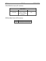
1
SMT365E
User Manual
User Manual (QCF42); Version 3.0, 5/2/01; © Sundance Multiprocessor Technology Ltd. 2001
Version 2.1
Page 2 of 26
SMT365e User Manual
Revision History
Date
Comments
Engineer
Version
18/07/02
First rev, based on 361
GP
1.0.0
06/01/03
User manual updated, 2 SHBs
YC
1.0.1
16/01/03
Changed flash to 4Mbyte
GP
1.0.2
20/01/03
Added FPGA pin-out
GP
1.0.3
31/01/03
Changed CPLD hdr pin-out.
GP
1.0.4
Set DSP clk=600, emif clk=100
24/02/03
No more SDBs clock selection
JPA
1.0.5
17/03/03
Added location of SDBs on the board.
JPA
1.0.6
Updated FPGA memory mapping.
24/04/03
Updated Data Sheets (Hyperlinks) section
JPA
1.0.7
19/09/03
Updated Data Sheets (Hyperlinks) section
JPA
1.0.8
Updated Reprogramming chapter
09/08/05
Update: the user manual supports the new
firmware implementation V3.0 (XC2V6000)
and the firmware V1.0 (XC2V8000)
SM
2.0
25/01/06
Errata: Flash ROM access
SM
2.1
16/02/06
Update: the user manual supports the new
firmware implementation for 2xSDBs, 32bits
V3.12 (XC2V6000)
AL
2.2
Version 2.1
Page 3 of 26
SMT365e User Manual
Table of Contents
Revision History ....................................................................................................... 2
Contacting Sundance............................................................................................... 4
Notational Conventions ........................................................................................... 5
DSP ........................................................................................................................ 5
SDB ........................................................................................................................ 5
SHB ........................................................................................................................ 5
Register Descriptions .............................................................................................. 5
Outline Description .................................................................................................. 6
Intended Audience ................................................................................................... 6
Block Diagram .......................................................................................................... 7
Architecture Description.......................................................................................... 8
DSP ............................................................................................................................ 8
Boot Mode............................................................................................................... 8
EMIF Control Registers........................................................................................... 9
SDRAM ................................................................................................................... 9
FLASH .................................................................................................................. 10
Virtex FPGA............................................................................................................. 11
Version control ...................................................................................................... 11
Firmware versions.................................................................................................. 11
Reprogramming the firmware and boot code ...................................................... 11
Comports................................................................................................................. 12
SHB .......................................................................................................................... 12
Global bus ............................................................................................................... 12
LED Setting ............................................................................................................. 13
LED Register......................................................................................................... 13
CONFIG & NMI ........................................................................................................ 14
Config Register ..................................................................................................... 14
Timer........................................................................................................................ 15
Timer Control Register .......................................................................................... 15
IIOF interrupt........................................................................................................... 16
Code Composer...................................................................................................... 17
Version 2.1
Page 4 of 26
SMT365e User Manual
Application Development....................................................................................... 17
SMT6400 .............................................................................................................. 17
3L Diamond........................................................................................................... 17
SMT6500 .............................................................................................................. 17
Operating Conditions ............................................................................................. 18
Safety.................................................................................................................... 18
EMC ...................................................................................................................... 18
General Requirements .......................................................................................... 18
Power Consumption.............................................................................................. 18
Connector Positions .............................................................................................. 19
Serial Ports & Other C60 I/O .................................................................................. 20
FPGA and CPLD JTAG ........................................................................................... 20
Virtex Memory Map................................................................................................. 21
SHB pin-out........................................................................................................... 23
SHB generic pin-out .............................................................................................. 23
FPGA PROG Pin Control (JP7 connector)............................................................ 24
DSP Boot Mode Control (JP6 connector).............................................................. 24
Bibliography............................................................................................................ 25
INDEX ...................................................................................................................... 26
Contacting Sundance
You can contact Sundance for additional information by login onto the Sundance
support forum.
Version 2.1
Page 5 of 26
SMT365e User Manual
Notational Conventions
DSP
The terms DSP, C64xx and TMS320C64xx will be used interchangeably throughout
this document.
SDB
The term SDB will be used throughout this document to refer to the Sundance Digital
Bus interface.
SHB
The term SHB will be used throughout this document to refer to the Sundance Highspeed Bus interface.
Register Descriptions
The format of registers is described using diagrams of the following form:
31–24
23–16
15–8
7–0
R,00000000
R,10000000
OFLAGLEVEL
R,00000000
RW,10000000
The digits at the top of the diagram indicate bit positions within the register and the
central section names bits or bit fields. The bottom row describes what may be done
to the field and its value after reset. Shaded fields are reserved and should only ever
be written with zeroes.
R
Readable by the CPU
W
Writeable by the CPU
RW
Readable and writeable by the CPU
Binary digits indicate the value of the field after reset
Version 2.1
Page 6 of 26
SMT365e User Manual
Outline Description
The SMT365 is a DSP module, size 2 TIM offering the following features:
TMS320C6416 processor running at 600MHz
Six comports
256MB of SDRAM (100MHz)
4MB of Flash ROM
Global Bus connector
6 SHB connectors for high-speed data transfer
Intended Audience
There are two existing versions of the firmware for the SMT365e.
For each of the versions of the different firmware is loaded in the FPGA:
-
Firmware version 1.1 or
-
Firmware version 1.2
This user manual covers the version 1.2 of the firmware for the SMT365e
implemented with the model described in the SMT6500 help file.
Refer to section Firmware versions.
Version 2.1
Page 7 of 26
SMT365e User Manual
Block Diagram
The following drawing shows the block diagram of the SMT365e module.
The main components of the SMT365e are:
-
A Texas Instruments DSP
-
One Xilinx FPGA Virtex-II device
-
256MB of SDRAM
2x Comm-Ports/SDL
26 I/O pins
JTAG Header
X-Checker Header
4 LEDs &
4 I/O pins
McBSP/Utopia/
GPIO
FPGA Controller
171 pins
'C6416
DSP
525 pins
256Mbytes SDRAM
4x Comm-Port/SDL
52 I/O pins
360 pins
Virtex-II, FF1152
824 I/O pins - Used 776
XC2V6000
1.5V
Global Bus
74 I/O pins
Sundance High-speed Bus
60-way Samtec x 6
Timer,& Control
15 I/O pins
J1 Top Primary TIM
Connector
Comm-Port 0 & 3
DC-DC Converters for DSP
and FPGA cores
J3 Global
Expansion
Connector
J2 Bottom Primary
TIM Connector
Comm-Port 1;2;5;4
Flash
4 LEDs
+ GPIO
Oscillator
Version 2.1
Page 8 of 26
SMT365e User Manual
Architecture Description
DSP
The Texas Instruments DSP can run at up to 600MHz. The DSP is doted of 256MB
of Synchronous DRAM (SDRAM).
The DSP is a TMS320C6416 type.
This is a fixed-point digital signal processor provided by Texas Instruments. The
processor will run with zero wait states from internal SRAM. The internal memory is
1MB in size and can be partitioned between normal SRAM and L2 cache.
An on-board crystal oscillator provides the clock used for the DSP which them
multiplies this by twelve internally.
Boot Mode
The DSP is connected to the on-board flash ROM that contains the Sundance
bootloader and the FPGA bitstream.
Following reset, the DSP will automatically load the data from the flash ROM into its
internal program memory at address 0 and then start executing from there. All this
code is the Sundance bootloader, and it is made up of two parts: FPGA configuration
and processor configuration. FPGA configuration uses data in the ROM to configure
the FPGA. A processor configuration sets the processor into a standard state by
writing into the DSP internal registers of the EMIF. Then it configures the FPGA from
the data held in the flash ROM.
The bootloader is executed. It will continually check the six comports until data
appears on one of them. This will next load a program in boot format from this
comport. Note that the bootloader will not read data arriving on other comports.
Finally the control is passed to the loaded DSP application.
The DSP will take approximately about 46s to configure the FPGA following reset,
assuming a 600MHz clock. The external devices implemented in the FPGA (such as
comports) must not be used during this configuration.
It is safest to wait for the configuration to complete. Note that comports will appear to
be "not ready" until the FPGA has been configured.
The FPGA programming algorithm is not described here. It can be found in the boot
code.
Version 2.1
Page 9 of 26
SMT365e User Manual
EMIF Control Registers
The DSP has two external memory interfaces (EMIF) which are 64 bits wide and 16
bits wide.
The DSP contains several registers that control the external memory interface
(EMIF). A full description of these registers can be found in the DSP C6000
Peripherals Reference Guide.
The standard bootstrap will initialise these registers to use the following resources:
Memory space
Resource
Address range
(EMIFA)
Internal program memory 0x00000000 - 0x000FFFFF
(1MB)
CE0
SDRAM
0x80000000 - 0x8FFFFFFF
CE1
Virtex
0x90000000 - 0x9FFFFFFF
Memory space
Resource
Address range
(EMIFB)
CE0
Flash paging control
0x60000000 – 0x60000200
CE1
4MB Flash (1st half)
0x64000000 – 0x640FFFFF
CE2
4MB Flash (2nd half)
0x68000000 – 0x680FFFFF
CE3
FPGA Configuration control
0x6C000000 – 0x6C000002
SDRAM
Memory space CE0 is used to access 256MB of SDRAM over EMIFA.
The speed of the SDRAM is dependent on the processor variant. Using the C6416,
the SDRAM will operate at 133MHz maximum. It operates at one sixth of the core
clock speed.
The EMIFA CE0 memory space control register should be programmed with the
value 0x000000D0 (64 bits SDRAM).
Version 2.1
Page 10 of 26
SMT365e User Manual
FLASH
A 4MB of Flash ROM is connected to the DSP in the EMIFB CE1 & CE2 memory
spaces. The ROM holds boot code for the DSP, configuration data for the FPGA, and
optional user-defined code.
The EMIFB CE1 and CE2 space control registers should be programmed with the
values 0x00000030 and 0xFFFFFF23 respectively.
As the DSP only provides 20 address lines on its EMIFB, both CE1 & CE2 are used
to access this device. This in itself allows the direct access to 2MB. A paging
mechanism is used to select which half of the 4MB device is visible in this 2MB
window.
As the EMIFB CE1 & CE2 memory spaces alias throughout the available range, the
flash device can be accessed using the address range 0x67E00000-0x681FFFFF.
This gives a 2MB continuous memory space.
Selecting the visible flash memory page (2 pages of 2MB) involves writing to the
following addresses as shown (the data written is irrelevant):
Address
Flash page selected
0x60000000
Page 0
0x60000100
Page 1
The EMIFB CE0 memory space control register should be programmed with the
value 0xFFF0C003.
Version 2.1
Page 11 of 26
SMT365e User Manual
Virtex FPGA
The FPGA (Field Programmable Gate Array) is a Xilinx Virtex-II device XC2V6000.
It implements the following communication resources:
•
Six Comport interfaces
•
Four 16-bit Sundance Digital Bus interfaces
•
One Global Bus interface
Version control
Revision numbers for both the boot code and FPGA firmware are stored in the Flash
ROM during programming as zero-terminated ASCII strings.
The SMT6001 utility can be used to display the version numbers of the bootloader
and the FPGA data.
Firmware versions
The SMT6001 utility includes the latest version of the bootloader and the latest
version of the FPGA data that implements the FPGA architecture described in the
SMT6500 help file.
Customers who wish to use the old firmware can obtain it from our support web
forum.
Reprogramming the firmware and boot code
The contents of the flash ROM are managed using the SMT6001 utility. This includes
the latest firmware and bootloader along with complete documentation on how to
reprogram the ROM. The utility assumes that you have Code Composer Studio
installed and that it has been configured correctly for the installed TIMs. The
Sundance Wizard can help you with this.
To confirm that the ROM has been programmed correctly, you should run the
confidence test in the BoardInfo utility (SMT6300).
Version 2.1
Page 12 of 26
SMT365e User Manual
Comports
The DSP has six comports, numbered 0 to 5.
The addresses of the Comport registers are described in the SMT6400 help file.
SHB
The SMT365e has six SHB connectors, all of which are connected to the DSP to give
16-bit/32-bit SDB interfaces on two SHB connectors. These interfaces operate with a
fixed clock rate of 100MHz.
Note that the four other SHB connectors are not used.
The following figure shows their localisation on the board:
SDB2
SHB_B
SDB3
SDB0
SHB_A
SDB1
Global bus
The SMT365e provides a single global bus interface. This is only accessible from the
DSP. The addresses of the global bus registers are shown in the Virtex Memory Map,
and are described in the SMT6400 help file.
Version 2.1
Page 13 of 26
SMT365e User Manual
LED Setting
The SMT365e has 13 LEDs. One shows the FPGA configuration status and the other
4 are under DSP control.
LED D6 always displays the state of the FPGA DONE pin. This LED is off when the
FPGA is configured (DONE=1) and on when it is not configured (DONE=0).
This LED should go on when the board is first powered up and go off when the FPGA
has been successfully programmed (this is the standard operation of the boot code
resident in the flash memory device). If the LED does not light at power-on, check
that you have the mounting pillars and screws fitted properly. If it stays on, the DSP
is not booting correctly, or is set to boot in a non-standard way.
Four of the remaining LEDs can be controlled with the LED register (D11, D12, D13,
D14). Writing 1 will illuminate the LED; writing 0 will turn it off.
Note that the LEDs D7-D10 are not used.
LED Register
(0x900D0000)
31–4
7
RW,0
6
RW,0
5
RW,0
4
RW,0
3
2
1
0
LED
D11
LED
D12
LED
D13
LED
D14
RW,0
RW,0
RW,0
RW,0
The four remaining LEDs (D2-5) are connected to the C60’s GPIO pins 12-15.
Version 2.1
Page 14 of 26
SMT365e User Manual
CONFIG & NMI
The TIM specification describes the operation of an open-collector type signal
CONFIG that is driven low after reset.
This signal, on a standard C4x based TIM, is connected to the processor’s IIOF3 pin.
On the SMT365, the CONFIG signal is asserted after power on, and can be released
by writing the value (1<<6) to the config register. Conversely, CONFIG may be reasserted by writing 0 to this bit. It is not possible for software to read the state of the
CONFIG signal.
The NMI signal from the TIM connector can be routed to the DSP NMI pin.
WARNING: Several software components include code sequences that assume
setting GIE=0 in the DSP CSR will inhibit all interrupts; NMI violates that assumption.
If an NMI occurs during such code sequences it may not be safe to return from the
interrupt. This may be particularly significant if you are using the compiler’s software
pipelining facility.
Config Register
31–8
Field
CONFIG
NMI
7
6
NMI
CONFIG
Description
0
drive CONFIG low
1
tri-state CONFIG
0
Disconnect NMI from the DSP
1
Connect NMI from TIM to the DSP.
Config and NMI DSP lines are described in the SMT6400 help file.
5–0
Version 2.1
Page 15 of 26
SMT365e User Manual
Timer
The TIM TCLK0 and TCLK1 signals can be routed to the DSP’s TOUT/TINP pins.
The signal direction must be specified, together with the routing information in the
timer control register.
Timer Control Register
Field
31–6
5
4
3–0
Reserved
TCLK1
TCLK0
Reserved
Description
TCLK0
TCLK1
0
TIM TCLK0 is an input
1
Enable TIM TCLK0 as an output
0
TIM TCLK1 is an input
1
Enable TIM TCLK1 as an output
If the TIM TCLKx pin is selected as an output, the DSP TOUTx signal will be used to
drive it. The TIM TCLKx pin will always drive the DSP TINPx input.
TCLK0EN
C6x
TOUT0
TINP0
TCLK0
FPGA
The Timer control register is described in the SMT6400 help file.
Version 2.1
Page 16 of 26
SMT365e User Manual
IIOF interrupt
The firmware can generate pulses on the external interrupt lines of the TIM.
Only the interrupt line IIOF1 and IIOF2 are connected from/to the DSP and the
HOST.
•
IIOF1 is connected from the DSP side to the HOST side: so, the DSP
interrupts the HOST
•
IIOF2 is connected from the HOST side to the DSP side: so, the HOST
interrupts the DSP
The IIOF interrupt lines are described in the SMT6400 help file.
Version 2.1
Page 17 of 26
SMT365e User Manual
Code Composer
This module is fully compatible with the Code Composer Studio debug and
development environment. This extends to both the software and JTAG debugging
hardware. The driver to use is the tixds64xx_11.dvr. CCS version 3.0 or later is
required as the reprogramming utility (SMT6001) requires it.
Troubleshooting
Our Knowledge data base and FAQ sections may help you to resolve some known
issues.
Application Development
Depending on the complexity of your application, you can develop code for SMT365
modules in several ways.
SMT6400
For simple applications, the Sundance SMT6400 software support package (project
examples) and its associated header files (SmtTim.h and ModSup.h) can suffice.
The SMT6400 product is installed by the Sundance Wizard and it is free of charge.
3L Diamond
This module is fully supported by 3L Diamond, which Sundance recommends for all
but the simplest of applications. A SMT365e has to be declared as appropriate in
configuration files as one processor of type:
•
SMT365E
SMT6500
This is the support package for the FPGA. It may be used to develop your application
in the FPGA of the module.
Version 2.1
Page 18 of 26
SMT365e User Manual
Operating Conditions
Safety
The module presents no hazard to the user.
EMC
The module is designed to operate within an enclosed host system that provides
adequate EMC shielding. Operation within the EU EMC guidelines is only guaranteed
when the module is installed within an appropriate host system.
The module is protected from damage by fast voltage transients introduced along
output cables from outside the host system.
Short-circuiting any output to ground does not cause the host PC system to lock up
or reboot.
General Requirements
The module must be fixed to a TIM40-compliant carrier board.
The SMT365e TIM is in a range of modules that must be supplied with a 3.3V power
source. In addition to the 5V supply specified in the TIM specification, these new
generation modules require an additional 3.3V supply to be presented on the two
diagonally-opposite TIM mounting holes. The lack of this 3.3V power supply should
not damage the module, although it will obviously be inoperable; prolonged operation
under these circumstances is not recommended.
The SMT365e is compatible with all Sundance TIM carrier boards. It is a 5V tolerant
module, and as such, it may be used in mixed systems with older TIM modules,
carrier boards and I/O modules.
Use of the TIM on SMT327 (cPCI) motherboards may require a firmware upgrade. If
LED D6 on the SMT365e remains illuminated once the TIM is plugged in and
powered up, the SMT327 needs the upgrade. The latest firmware is supplied with all
new boards shipped. Please contact Sundance directly if you have an older board
and need the upgrade.
The external ambient temperature must remain between 0°C and 40°C, and the
relative humidity must not exceed 95% (non-condensing).
Power Consumption
The power consumption of this TIM is dependent on the operating conditions in terms
of core activity and I/O activity. The maximum power consumption is 10W.
Version 2.1
Connector Positions
Page 19 of 26
SMT365e User Manual
Version 2.1
Page 20 of 26
SMT365e User Manual
Serial Ports & Other C60 I/O
The C60 contains various I/O ports. These signals are connected to a 0.1” pitch DIL
pin header. The pin-out of this connector is shown here:
P
DR0
FSR0
DX0
FSX0
CLKR0
CLKX0
CLKS0
CLKS1
CLKX1
CLKR1
URA3
URA4
URA2
CLKS2
DX1
FSX1
GPIO8
UXA4
O
L
DR2
FSR2
DX2
FSX2
CLKR2
CLKX2
A
R
URA1
URA0
FSR1
DR1
UXA0
UXA3
UXA2
UXA1
URD0
URD1
URD2
URD3
URD4
URD5
URD6
URD7
URCLK
URENB
URCLAV
URSOC
UXD0
UXD1
UXD2
UXD3
UXD4
UXD5
UXD6
UXD7
UXCLK
UXENB
UXCLAV
UXSOC
NC
GPIO9
GPIO10
GPIO11
GPIO12
GPIO13
GPIO14
GPIO15
V33
V33
TTL2
TTL3
GPIO0
GPIO1
GPIO2
GPIO3
GPIO4
GPIO5
GPIO6
GPIO7
GND
GND
TTL0
TTL1
I
S
A
T
I
O
N
FPGA and CPLD JTAG
The following shows the pin-outs for JP2 (CPLD) and JP3 (FPGA) JTAG connectors:
Signal
Pin
Pin
Signal
V33
1
4
TMS
TCK
2
5
TDO
GND
3
6
TDI
Version 2.1
Page 21 of 26
SMT365e User Manual
Virtex Memory Map
#define SMT365eCP0
(volatile unsigned int *)0x90000000
#define SMT365eCP1
(volatile unsigned int *)0x90008000
#define SMT365eCP2
(volatile unsigned int *)0x90010000
#define SMT365eCP3
(volatile unsigned int *)0x90018000
#define SMT365eCP4
(volatile unsigned int *)0x90020000
#define SMT365eCP5
(volatile unsigned int *)0x90028000
#define SMT365eCP0_STAT
(volatile unsigned int *)0x90004000
#define SMT365eCP1_STAT
(volatile unsigned int *)0x9000C000
#define SMT365eCP2_STAT
(volatile unsigned int *)0x90014000
#define SMT365eCP3_STAT
(volatile unsigned int *)0x9001C000
#define SMT365eCP4_STAT
(volatile unsigned int *)0x90024000
#define SMT365eCP5_STAT
(volatile unsigned int *)0x9002C000
#define SMT365eGB_STAT
(volatile unsigned int *)0x90034000
#define SMT365eSDB_STAT
(volatile unsigned int *)0x90038000
#define SMT365eSTAT
(volatile unsigned int *)0x9003C000
#define SMT365eSDBA
(volatile unsigned int *)0x90040000
#define SMT365eSDBB
(volatile unsigned int *)0x90050000
#define SMT365eSDBC
(volatile unsigned int *)0x90060000
#define SMT365eSDBD
(volatile unsigned int *)0x90070000
#define SMT365eSDBA_STAT
(volatile unsigned int *)0x90048000
#define SMT365eSDBB_STAT
(volatile unsigned int *)0x90058000
#define SMT365eSDBC_STAT
(volatile unsigned int *)0x90068000
#define SMT365eSDBD_STAT
(volatile unsigned int *)0x90078000
#define SMT365eSDBA_INPUTFLAG
(volatile unsigned int *)0x90044000
#define SMT365eSDBB_INPUTFLAG
(volatile unsigned int *)0x90054000
#define SMT365eSDBC_INPUTFLAG
(volatile unsigned int *)0x90064000
#define SMT365eSDBD_INPUTFLAG
(volatile unsigned int *)0x90074000
#define SMT365eSDBA_OUTPUTFLAG
(volatile unsigned int *)0x9004C000
#define SMT365eSDBB_OUTPUTFLAG
(volatile unsigned int *)0x9005C000
#define SMT365eSDBC_OUTPUTFLAG
(volatile unsigned int *)0x9006C000
#define SMT365eSDBD_OUTPUTFLAG
(volatile unsigned int *)0x9007C000
#define GLOBAL_BUS
(volatile unsigned int *)0x900A0000
#define GLOBAL_BUS_CTRL
(volatile unsigned int *)0x90080000
#define GLOBAL_BUS_START
(volatile unsigned int *)0x90088000
#define GLOBAL_BUS_LENGTH
(volatile unsigned int *)0x90090000
Version 2.1
Page 22 of 26
SMT365e User Manual
#define SMT365eTCLK
(volatile unsigned int *)0x900C0000
#define SMT365eTIMCONFIG
(volatile unsigned int *)0x900C8000
#define SMT365eLED
(volatile unsigned int *)0x900D0000
#define SMT365eINTCTRL4
(volatile unsigned int *)0x900E0000
#define SMT365eINTCTRL4_EXT
(volatile unsigned int *)0x900E4000
#define SMT365eINTCTRL5
(volatile unsigned int *)0x900E8000
#define SMT365eINTCTRL5_EXT
(volatile unsigned int *)0x900EC000
#define SMT365eINTCTRL6
(volatile unsigned int *)0x900F0000
#define SMT365eINTCTRL6_EXT
(volatile unsigned int *)0x900F4000
#define SMT365eINTCTRL7
(volatile unsigned int *)0x900F8000
#define SMT365eINTCTRL7_EXT
(volatile unsigned int *)0x900FC000
Version 2.1
Page 23 of 26
SMT365e User Manual
SHB pin-out
SHB generic pin-out
QSH Pin number
Hw
CLK
1
2
D0
D1
3
4
D2
D3
5
6
D4
D5
7
8
D6
D7
9
10
D8
D9
11
12
D10
D11
13
14
D13
15
16
D14
D15
17
18
USERDEF0
USERDEF1
19
20
USERDEF2
USERDEF3
21
22
WEN
REQ
23
24
ACK
25
26
27
28
29
30
31
32
33
34
35
36
CLK
37
38
D0
D1
39
40
D2
D3
41
42
D4
D5
43
44
D6
D7
45
46
D8
D9
47
48
D10
D11
49
50
D13
51
52
D14
D15
53
54
USERDEF0
USERDEF1
55
56
USERDEF2
USERDEF3
57
58
WEN
REQ
59
60
ACK
Hw0
QSH Pin number
Hw1
Hw1
Hw0
Hw
D12
D12
Note: Hw is a short for Half-word (i.e. 16-bit Word)
This standard is implemented using SAMTEC QSTRIP 0.50mm Hi-speed connectors.
Version 2.1
Page 24 of 26
SMT365e User Manual
FPGA PROG Pin Control (JP7 connector)
Jumper Position
1-2
2-3
Out
PROG asserted
continuously
PROG asserted for the
duration of RESET.
PROG under control of
DSP
Can also be controlled
by the DSP.
DSP Boot Mode Control (JP6 connector)
In
DSP will boot from flash
Out
DSP will be set to boot from HPI
Version 2.1
Page 25 of 26
SMT365e User Manual
Bibliography
1. Sundance Help file
2. SMT6400 help file (DSP support package) and SMT6500 help file (FPGA support package)
3. TMS320C6000 Peripherals Reference Guide (literature number SPRU190)
It describes common peripherals available on the TMS320C6000 digital signal processors. This
book includes information on the internal data and program memories, the external memory
interface (EMIF), the host port, multichannel-buffered serial ports, direct memory access (DMA),
clocking and phase-locked loop (PLL), and the power-down modes.
4. TIM-40 MODULE SPECIFICATION Including TMS320C44 Addendum
5. SDB Technical Specification
6. SHB Technical Specification
7. TMS320C4x User's Guide (literature number SPRU063)
It describes the C4x 32-bit fixed-point processor, developed for digital signal processing as well as
parallel processing applications. Covered are its architecture, internal register structure, instruction
set, pipeline, specifications, and operation of its six DMA channels and six communication ports.
Software and hardware applications are included.
8. Xilinx Virtex-II datasheet
9. TMSC6416 datasheet
Version 2.1
Page 26 of 26
SMT365e User Manual
INDEX
LED register · 13
A
N
Application Development · 17
Architecture Description · 8
Notational Conventions · 5
B
O
Bibliography · 25
Block Diagram · 7
Boot Mode · 8
Operating Conditions · 18
P
C
Power consumption · 18
Code Composer · 17
Comport · 12
CONFIG & NMI · 14
R
Register Descriptions · 5
E
EMIF Control Registers · 9
F
Firmware Reprogramming · 11
Firmware versions · 11
Flash · 10
S
SDRAM · 9
Serial Ports · 20
SHB · 12
SMT6400 · 17
SMT6500 · 17
T
I
Timer · 15
IIOF lines · 16
V
L
LEDs · 13
Version Control · 11
Virtex
memory map · 21