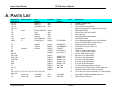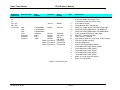
1
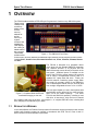
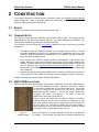
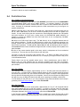
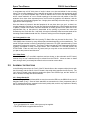
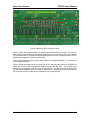
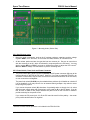
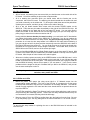
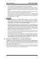
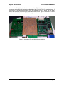
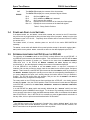
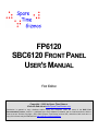
FP6120 SBC6120 FRONT PANEL USER'S MANUAL First Edition Copyright 2003 by Spare Time Gizmos. Visit our web site at www.SpareTimeGizmos.com Permission is granted to copy, distribute and/or modify this document under the terms of the GNU Free Documentation License, Version 1.1 published by the Free Software Foundation; with no invariant sections; with the front cover text “Portions Copyright 2001-2003 by Spare Time Gizmos” and our URL, and with no back cover text. A copy of this license may be obtained from http://www.gnu.org/licenses/fdl.txt. CONTENTS 1 OVERVIEW ................................................................................................................................. 1 1.1 REGULATORY WARNING ...................................................................................................... 1 1.2 WARRANTY ......................................................................................................................... 2 2 CONSTRUCTION .......................................................................................................................... 3 2.1 ERRATA .............................................................................................................................. 3 2.2 FIRMWARE NOTES ............................................................................................................... 3 2.3 SBC6120 MODIFICATIONS .................................................................................................. 3 2.4 PARTS SELECTION............................................................................................................... 4 2.5 ASSEMBLY INSTRUCTIONS.................................................................................................... 5 2.6 INSTALLING THE SBC6120 AND OTHER DAUGHTER BOARDS ................................................. 9 3 OPERATION .............................................................................................................................. 12 3.1 INDICATORS ...................................................................................................................... 12 3.2 SWITCHES ......................................................................................................................... 12 3.3 ROTARY SWITCH ............................................................................................................... 13 3.4 POWER AND PANEL LOCK SWITCHES.................................................................................. 14 3.5 DIFFERENCES BETWEEN THE FP6120 AND THE PDP-8/E.................................................... 14 A. PARTS LIST .......................................................................................................................... 16 Page i Spare Time Gizmos FP6120 User's Manual 1 OVERVIEW The FP6120 adds a traditional PDP-8/E style Programmer’s Console to any SBC6120 system. Twenty seven LEDS provide continuous display of the current memory address as well as memory or register contents, and a additional LED displays the running or halted state of the processor. Twelve data Figure 1 - The SBC6120 Front Panel switches allow for direct entry of binary data and an additional eight switches provide program control functions including BOOT, ADDRESS LOAD, EXTENDED ADDRESS LOAD, CLEAR, CONTINUE, EXAMINE, DEPOSIT and HALT. The FP6120 is designed as a peripheral device which plugs into the standard SBC6120 expansion bus, however because of its physical size the SBC6120 actually mounts directly to the back of the front panel. Additional space is available on the back of the FP6120 to mount another I/O board as well as either a CompactFlash memory card or a standard 2½” laptop hard disk drive. Finally, the FP6120 contains a switching power supply which can supply all necessary power for the SBC6120, one or two daughter boards, and the FP6120 itself from a single unregulated source of +9 to +12VDC. The front panel façade you see in these photos was professionally screen printed in five colors and then Figure 2 - Complete SBC6120/FP6120 laser cut for the switch openings. The entire combination hanging on the wall FP6120 and SBC6120 assembly, including a hard disk drive, is less than 2” thick and can be framed like a painting and hung on the wall. Just imagine it – a complete PDP-8/E clone, including disk drive, hanging on the wall above your desk! 1.1 REGULATORY WARNING In the United States, the Federal Communications Commission requires that devices that use and radiate radio frequency energy be certified in accordance with CFR Title 47, Parts 2 and 15. Other countries will have different requirements. 10/24/2003 8:39 PM Page 1 Spare Time Gizmos FP6120 User's Manual The FP6120 design is not in finished product form and has NOT been approved by the FCC or any other regulatory agency worldwide. The user understands that approvals may be required prior to the operation of the FP6120, and agrees to utilize the FP6120 in keeping with all laws governing its operation in the country of use. 1.2 WARRANTY SPARE TIME GIZMOS OFFERS NO WARRANTY, EXPRESS OR IMPLIED, AS TO THE RELIABILITY OR ACCURACY OF THE FP6120 DESIGN. SPARE TIME GIZMOS OFFERS NO WARRANTY, EXPRESS OR IMPLIED, AS TO THE ACCURACY OF THE INFORMATION PRESENTED IN THIS DOCUMENT. SPARE TIME GIZMOS OFFERS NO WARRANTY, EXPRESS OR IMPLIED, AS TO THE SUITABILITY OR CORRECTNESS OF ANY SOFTWARE OR FIRMWARE SUPPLIED IN CONJUNCTION WITH THE FP6120. SPARE TIME GIZMOS MAKES NO REPRESENTATIONS AS TO THE SUITABILITY OF THE FP6120 FOR ANY APPLICATION. IT IS SOLELY AND EXCLUSIVELY YOUR RESPONSIBILITY TO EVALUATE THE ACCURACY, COMPLETENESS, AND USEFULNESS OF THE FP6120 AND ALL RELATED DESIGNS, SOFTWARE, AND OTHER INFORMATION PROVIDED BY SPARE TIME GIZMOS. THE ENTIRE RISK AS TO THE USE AND PERFORMANCE OF THE FP6120 IS ASSUMED SOLELY BY YOU. NO REPRESENTATION OR OTHER AFFIRMATION OF FACT, INCLUDING, BUT NOT LIMITED TO, STATEMENTS REGARDING CAPACITY, PERFORMANCE OF PRODUCTS, OR SUITABILITY FOR USE, WHETHER MADE BY SPARE TIME GIZMOS EMPLOYEES OR OTHERWISE, WILL BE DEEMED TO BE A WARRANTY FOR ANY PURPOSE, OR GIVE RISE TO ANY LIABILITY ON THE PART OF SPARE TIME GIZMOS. THE WARRANTIES AND CORRESPONDING REMEDIES AS STATED IN THIS SECTION ARE EXCLUSIVE AND IN LIEU OF ALL OTHERS, WRITTEN OR ORAL. SOME JURISDICTIONS DO NOT ALLOW THE EXCLUSION OF IMPLIED WARRANTIES, SO THE ABOVE EXCLUSION MAY NOT APPLY TO YOU. THE LIMITED WARRANTIES AND CONDITION REFERENCED ABOVE GIVE YOU SPECIFIC LEGAL RIGHTS. YOU MAY HAVE OTHERS, WHICH VARY FROM JURISDICTION TO JURISDICTION. IN NO EVENT SHALL SPARE TIME GIZMOS OR ITS EMPLOYEES BE LIABLE FOR ANY COSTS OR DIRECT, INDIRECT, PUNITIVE, INCIDENTAL, SPECIAL, CONSEQUENTIAL DAMAGES OR ANY OTHER DAMAGES WHATSOEVER INCLUDING, WITHOUT LIMITATION, DAMAGES FOR COSTS OF PROCUREMENT OF SUBSTITUTE GOODS OR SERVICES, LOST PROFITS, LOSS OF DATA, INTERRUPTION OF BUSINESS, OR LOSS OF USE, ARISING OUT OF OR IN ANY WAY CONNECTED WITH THE USE OR PERFORMANCE OF THE FP6120 OR YOUR RELIANCE ON THE FP6120 OR RESULTS FROM MISTAKES, OMISSIONS, INTERRUPTIONS, DELETION OF FILES, ERRORS, DEFECTS, DELAYS IN OPERATION OR TRANSMISSION, OR ANY FAILURE OF PERFORMANCE WHETHER BASED ON CONTRACT, TORT, STRICT LIABILITY OR OTHERWISE, EVEN IF SPARE TIME GIZMOS HAS BEEN ADVISED OF THE POSSIBILITY OF DAMAGES. BECAUSE SOME STATES/JURISDICTIONS DO NOT ALLOW THE EXCLUSION OR LIMITATION OF LIABILITY FOR CONSEQUENTIAL OR INCIDENTAL DAMAGES, THE ABOVE LIMITATION MAY NOT APPLY TO YOU. IN NO EVENT SHALL SPARE TIME GIZMOS' LIABILITY, IN THE AGGREGATE, EXCEED THE SUMS ACTUALLY PAID BY YOU TO SPARE TIME GIZMOS AND ACCEPTED BY SPARE TIME GIZMOS FOR THE USE OF THE FP6120. 10/24/2003 8:39 PM Page 2 Spare Time Gizmos FP6120 User's Manual 2 CONSTRUCTION If you haven’t already, then please read the “Assembly” section of the SBC6120 User’s Manual before reading this. Many of the points made there, particularly the section on “Sockets and Soldering” apply equally well to the FP6120! 2.1 ERRATA There are no known errors in Revision D of the FP6120 board. 2.2 FIRMWARE NOTES The FP6120 requires that your SBC6120 have BTS6120 v266 or later. This version may be downloaded from the Spare Time Gizmos web site if you need to upgrade your EPROMs. The FP6120 does not require any changes to the SBC6120 PLDs. If you intend to use the FP6120 with Jim Kearney's IOB6120, there are more issues you should be aware of: • The IOB6120 requires a hardware upgrade to work reliably with the FP6120. The last few IOBs assembled and sold by Jim already had this modification, and if your IOB contains a 74HC373 part then yours should be OK. If it contains a 74ACT373, however, talk to Jim about the details of a fix. • Early versions of the FPGA bit stream include an implementation of the PDP-8 switch register which will conflict with the FP6120 and prevent the front panel switches from working. The latest version of the FPGA bit stream has the switch register removed and can be obtained from http://www.jkearney.com/sbc6120/iob6120.htm. Follow the instructions in Jim’s IOB6120 manual for downloading new FPGA bits to the Flash ROM on the IOB6120. • Although the FP6120 works with any SBC6120 PLD version, the IOB requires revision B or later of the IOT1 PLD. Spare Time Gizmos is currently shipping revision C of this part. Contact Jim directly for more information on these IOB updates. 2.3 SBC6120 MODIFICATIONS SBC6120 Revision D PC boards require that a jumper be added to connect the LXMAR signal to pin 22 of the expansion connector. Revision E and later PC boards incorporate this change and do not require modification. The revision of your PC board can be found in the etch on the solder side underneath the IDE connector – look for the words “SBC6120-2x Copyright 200? Spare Time Gizmos”. The letter “x” after the SBC6120-2 is the revision of your board. Figure 3 shows the proper way to modify a revision D PC board. Carefully count the pins on the bus connector to locate pin 22, and then count down four more pins to locate the trace that connects U8 pin 23 to U5 pin 34. This trace is LXMAR, and you need to solder a short jumper from it to pin 22 of the bus connector. Since pin 22 was previously unused, no other traces need to be cut. Figure 3 LXMAR Jumper Spare Time Gizmos is currently shipping Revision E of the SBC6120 PC boards. These boards, and later ones, already incorporate this 10/24/2003 8:39 PM Page 3 Spare Time Gizmos FP6120 User's Manual connection and do not require modification. 2.4 PARTS SELECTION 2.4.1 Finding Comp atible Switches The FP6120 is designed to use C&K P/N 7101J60V6BE1 (ON-NONE-ON) and 7108J60V6BE1 (ON-NONE-MOM) SPDT PCB mount paddle switches. It’s certainly possibly to find exact matches for these part numbers, however there are a number of other switches that can also be used. It's handy to understand something about the C&K nomenclature so you can figure out possible substitutions. J60 is the actuator style, in this case a 0.460" wide lever. Other styles in the same width, such as the J1, J15 or J50 rockers, will fit the PC board but probably won't work with the plastic front facade. It’s also worth nothing that the actuators are interchangeable between the C&K paddle and rocker switches, so if you have a cheap source for ON-NONE-ON paddle switches, it’s possible to remove the paddles from them and install them on the corresponding ON-NON(MOM) rocker switches. V6 refers to the PCB mount frame used. The V61 frame is for our purposes identical and will work without problems. The V3 and V31 frames are similar but with different mounting hole spacing, however the FP6120 PC board contains extra holes so that the V3 and V31 frames will also fit without problems. The V2 and V21, V4 and V41, V7, V8, and V9 frames will all fit the PC board however these frames are different heights and will not mate properly with the plastic front panel faceplate. B refers to the contact material (gold in this case), which is unimportant as far as mechanical concerns go. The only other one you're likely to see is Q, silver. The final 1 at the end of the P/N is the actuator color. 1 is White, 2 is Black, and 3 is Red. Naturally this makes to mechanical difference, but, for example, you might not like the way a row of all red switches looks! Finally, C&K is not the only possible switch source. Other manufacturers, such as NKK, ESwitch, CTS, etc. make switches that are generally compatible with their C&K counterparts. These manufacturers usually have some sort of cross reference guide to help you find equivalent part numbers. 2.4.2 The LED Bar The LED Bar is a piece of plastic, approximately 12.4"x1.1" and 5/8" thick with holes drilled in it for every LED. It mounts solder in swage standoffs placed on the PC board with #4-40 screws and serves two purposes. First, the LED bar serves as an "aligner" to keep the LEDs straight and lined up with the corresponding holes in the faceplate. Second, the bar isolates the LEDs so that the light from, say, the MA3 LED doesn't also leak out the opening for the MA2 or MA4 LEDs. You can build your own LED bar, or you can purchase a nicely milled and drilled one all ready to go directly from Spare Time Gizmos, part number FP6120-LBK. 2.4.3 The Faceplate The faceplate is a piece of 3/16” acrylic plastic, approximately 8 ½” by 15”, silk screened with the front panel graphics and cut to clear the switches. It mounts to the front panel PC board with eight #4-40 by 5/8” standoffs which are permanently attached to the faceplate. You can purchase a faceplate separately from Spare Time Gizmos, part number FP6120-FPK. In the faceplate supplied by Spare Time Gizmos the graphics are screen printed, with no less than five colors and five separate printing steps, onto a 15 mil (that's 0.015"!) polycarbonate film. 10/24/2003 8:39 PM Page 4 Spare Time Gizmos FP6120 User's Manual In a separate step a 3/16" thick piece of acrylic is laser cut to size and drilled for the mounting holes. The mounting hardware is then attached to the back of this panel and permanently glued into place. In yet a third separate step, a sheet of adhesive film is cut to size and then stamped with a custom made die to cut out circular openings in the exact size and position of the LED windows. Now, those three separate pieces, the film with the graphics, the adhesive, and the 3/16" panel are all laminated together into a single piece and finally the entire thing is laser cut again for the switch openings. One nice feature of process is that the faceplate is all one piece when you get it, so there's no complex assembly required on your part (like aligning and sandwiching a film between two sheets of plastic). Another nice feature is that the silkscreen is actually printed on the back side of the polycarbonate film, so that when it's assembled all the printing is protected from wear and scratches by the 15 mil thick film. And finally, this style of assembly hides leaves the heads of the mounting screws hidden beneath the film, so there’s nothing to mar the faceplate graphics. 2.4.4 Integrated Cir cuits Either the 74HC366 or 74HC368 Hex Inverting Tri-State buffer may be used in this circuit.1 The 7555 CMOS timer is known by many different part numbers depending on the manufacturer. The actual 7555 part number is used by Harris/Intersil, however the TLC555 (manufactured by Texas Instruments) is also quite common. The Power Trends (now part of Texas Instruments) switching regulator is available in either a 2A/10W version, the PT78HT205H or a 3A/15W version, the PT78HT305H. Either one will fit the PC board, and you may wish to use the 3A/15W device if you plan to also power a hard disk drive.2 2.4.5 Other Parts C2 and C7 are 0.01 µF monolithic capacitors and are shown on the schematic and PC board, however they are not needed and may be omitted from the FP6120. It does no harm to install them, though, and if you already have then there’s no need to remove them. 2.5 ASSEMBLY INSTRUCTIONS In the following instructions, the "front" of the PC board refers to the component side (the one with the silk screen) and the "back" of the PC board is the solder side (opposite the silk screen). The "top" of the PC board is the edge that contains the Spare Time Gizmos logo, and the "bottom" of the PC board is the edge with all the switches. 2.5.1 Swage Stand offs Solder in, swage, ⅛” by #4-40 standoffs are used to mount the LED bar, the SBC6120 and an I/O daughter board (if any). Some of these standoffs are mounted on the front (component) side of the PC board and some are mounted on the back (solder) side, and it’s very important to identify the correct holes for each standoff. 1 If you purchased the kit version, either part may be supplied. 2 The PT78HT205H is supplied with the full kit. 10/24/2003 8:39 PM Page 5 Spare Time Gizmos FP6120 User's Manual Figure 4 -Mounting Holes (Component Side) Figure 4 shows the component side of a partially assembled FP6120 PC board. The outline of the LED bar is shown and the seven swage standoffs used for mounting the LED bar are circled. These standoffs are all mounted with their threaded parts on the front (component) side of the PC board and are soldered on the back (solder) side. Figure 4 also shows the eight mounting holes used by the faceplate assembly. These holes do not use swage standoffs! Figure 5 shows the solder side of the same FP6120 PC board and the outlines of the SBC6120 board, the I/O board, the CompactFlash adapter, and the IDE disk drive. The colored circles indicate the corresponding mounting holes for each device. The SBC6120 and I/O board each use five swage standoffs, and in this case the standoffs are installed with their threaded part on the solder side of the PC board and are soldered on the component side. 10/24/2003 8:39 PM Page 6 Spare Time Gizmos FP6120 User's Manual Figure 5 - Mounting Holes (Solder Side) 2.5.2 Small Compo nents 9 Mount the small components, such as the IC sockets, resistors, capacitors, and the voltage regulator REG1, next. Above all, do not mount the LEDs, switches, or connectors now. 9 All the resistor packs used are the type that has one common pin. Be sure to mount them with the common pin as #1, which is indicated by a square pad on the PC board. You may wish to socket RP1 thru RP4 if you want to change them later to adjust the LED current3. RP5 thru RP8 are always 4.7K and there's no point in socketing them. 2.5.3 Power Switch , Panel Lock and Power Connector 9 The power switch (S1), panel lock switch (PLOCK) and DC power connector (J3) may all be mounted directly to the PF6120 PC board. However, if you plan to install the FP6120 in an enclosure of some kind it may be more convenient to mount these switches off the PC board, or even remove them all together. The panel lock switch (PLOCK) may be omitted without problems (it will default to unlocked if it is not installed) or you may connect it to an external switch (perhaps a key switch or some kind) using wire jumpers. If you mount the power switch (S1) elsewhere it’s probably easier to simply wire it in series with the power supply rather than connecting it to the pads for S1 on the PC board. If you do this, be sure to solder a wire jumper between the pads for S1 on the FP6120 PC board to provide continuity for the power circuit! If you mount the DC power jack, J1, off the PC board be careful of the polarity – the center pin is positive and the sleeve is negative! 3 Sockets for these resistor packs are not included in the FP6120 full kit. 10/24/2003 8:39 PM Page 7 Spare Time Gizmos FP6120 User's Manual 2.5.4 Bus Connect ors 9 J2 is a female, non-stacking bus connector which you should mount on the solder side of the PC board. You will be soldering its pins on the component side. 9 J1 is a stacking bus connector which you should mount with the female part on the component side of the PC board. The stacking pins should extend thru the solder side, and you solder it normally, on the solder side. Try to keep the solder down around the pads when soldering this connector, and don't get any solder on the ends of the pins. 9 J5 is a two pin female header which mates with the console CPREQ header on the SBC6120. That’s the two pin header immediately to the right of the HD6120 CPU chip. J5 should be installed on the back side of the front panel PC board. You may also need to replace the header on the SBC6120 with one that has longer pins (the wire wrap style are plenty long) to ensure that it makes connection with J54. Having said that, be sure that the pins aren't too long - you could crack the PC board when you tighten the mounting screws on the SBC6120! In particular, if you do you replace the header on the SBC6120 with a wire wrap version, the pins will be way too long! The best procedure is to insert the wire wrap header in the SBC6120 PC board without soldering it (you can use tape to hold it in place) and then temporarily mount the SBC6120 on the back of the FP6120 PC board (see section 0). You can push the pins on the wire wrap header thru the SBC6120 PC board until the correct length is achieved. Then solder them, remove the SBC6120 from the FP6120, and cut off the excess pin length. Don't confuse J5 with JP2 (the SLU Break Enable jumper) on the front panel PC board. JP2 is closer to the resistor and is a standard two pin header installed on the top of the front panel PC board. J5 is the pair of holes closest to the switch register. 9 J4 serves a similar purpose connecting to the CPREQ header on the IOB6120 board. In this case you should have installed a female header on the back side of your IOB and the male header on the back side of the front panel. This arrangement allows you to plug the IOB6120 into the SBC6120 directly, without a front panel, if you ever want to. You’ll have the same problems with the length for this pair of headers that you did for the SBC6120, and you can use the same techniques to solve it. At this point you should have all electronic components mounted EXCEPT the toggle switches, rotary switch and LEDs. 2.5.5 LED Bar and LEDs 9 Mount the plastic LED spacer bar using seven #4-40 x ⅝” flathead screws into the corresponding swage standoffs. The front of the LED bar is countersunk to fit the screw heads and the back side of the LED bar is recessed to fit the swage standoffs. The LED bar should fit snugly against the PC board and the screw heads should not protrude above the top of the LED bar. The LED Bar supplied by Spare Time Gizmos has five extra holes which are used to secure the piece during the machining process. These holes are easily identified because they are not countersunk or recessed, and they should be left empty. 9 Mount a group of five or six LEDs by pushing them thru the light bar from the front, Be sure to get the polarity right - the long lead goes to the hole marked with a + on the silk screen, 4 A two pin wire wrap header for replacing the one on the SBC6120 board is included in the FP6120 full kit. 10/24/2003 8:39 PM Page 8 Spare Time Gizmos FP6120 User's Manual After you've installed a few LEDs, carefully (so that they don't fall out!) flip the PC board over and lay it upside down on the workbench so that it is resting on the LED bar.. From the solder side, push the LEDs down until the LED face is pressing against the bench this will ensure that the face of each LED is exactly flush with the surface of the bar. Solder one lead on each LED, flip the assembly over and double check that everything is positioned properly. When you're satisfied with the LED position solder the other leads, and then repeat this procedure for another group of LEDs. Continue until all 26 are installed. Figure ?? shows a picture of the FP6120 with the LED bar, LEDs and other small components installed. Notice that the LEDs are flush with the LED bar – be especially careful that the LEDs do not protrude beyond the face of the LED bar, because they might crack the plastic faceplate when it is installed. 2.5.6 Switches 9 Install the paddle switches next – SR0 thru SR11 and HALT are "snap action", ON-NONEON switches and the rest are all momentary. The momentary switches should be installed so that their toggles point upward in the rest position; that is, you should push their levers down to activate them. The sole exception to this rule is the DEP switch which, by tradition, is installed "upside down" so that you have to lift the paddle to activate it. 9 Before installing the rotary switch you will need to cut the shaft to a length of approximately 0.400"??, as measured from the top of the threaded sleeve. To improve the front panel clearance, remove the lock washer from the shaft of the rotary switch. Do not remove the tang washer (that’s the washer with the little finger on it) and be sure to replace the nut after removing the lock washer; it prevents the tang washer from falling out. The tang washer limits the rotation of the switch to four positions, so if you do accidentally remove the tang washer, be sure to replace it with the finger in the hole marked #4. Notice that the rotary switch has a small round plastic "post" on the top surface that serves as a key. This key is shown on the PC board silk screen and should be about the 2 o'clock position when the switch is correctly installed. Clearance for the rotary switch is limited, so be sure it is absolutely flat against the PC board when you install it. At first solder only two terminals on opposite sides of the switch, and then use your soldering iron to re-melt the solder on those two terminals while you press the switch down against the PC board with your other hand. Visually inspect it to make sure that it is snug against the PC board before soldering the other terminals. 2.6 INSTALLING THE SBC6120 AND OTHER DAUGHTER BOARDS The SBC6120, and any I/O daughter board such as the IOB6120 mount to the back (solder) side of the FP6120 using #4-40 ½” nylon spacers inserted in the swage standoffs soldered to the PC board. The ½” length of the spacer plus the ⅛” length of the swage gives exactly the correct 0.625” height for these boards that will allow the bus connectors to mate properly. #-4-40 ⅜” nylon screws are used to complete the job. When installing either the SBC6120 or the IOB6120, be certain that the CPREQ headers mate correctly – the pins should line up with the corresponding female header and the pins must not be too long or too short. See section 2.5.4 for a complete description. 10/24/2003 8:39 PM Page 9 Spare Time Gizmos FP6120 User's Manual Note that the SBC6120 is installed in the center of the FP6120 “face down” – that is, with the component of the SBC6120 facing the solder side of the FP6120. The I/O expansion board, if any, installs on the right side of the back of the FP6120 “back to back” – that is, with the solder side of the expansion board facing the solder side of the FP6120. Figure 6 illustrates the correct installation of the SBC6120 and an IOB6120 daughter card. Figure 6 - Assembled FP6120, SBC6120 and IOB6120 10/24/2003 8:39 PM Page 10 Spare Time Gizmos FP6120 User's Manual 3 OPERATION 3.1 INDICATORS The FP6120 contains a total of twenty eight LED indicators. These indicators provide a continuous display of the memory address, memory data and the contents of several internal processor registers, as described in table Table 1. MEMORY ADDRESS Displays the currently addressed memory location while the processor is running, the contents of the program counter when the processor stops, and the address of the location corresponding to the memory data displayed when the rotary switch is set to the MD position. EMA These LEDs are unused in conjunction with the MEMORY ADDRESS LEDs to display a full fifteen bit memory address. DATA These twelve LEDs can display either the contents of the memory location indicated by the MEMORY ADDRESS and EMA LEDs, or the contents of the internal processor accumulator or multiplier quotient registers, or the processor status flags, as selected by the position of the rotary switch. RUN This LED is ON when the processor is executing a main memory program and it is OFF when BTS6120 has control. Table 1 - Front Panel Indicators 3.2 SWITCHES The FP6120 contains a total of twenty paddle switches for memory modification, program control and data entry functions. Most switches are effective only when the RUN LED is OFF (i.e. BTS6120 is in control) and only the switch register, SR0..SR11, the rotary switch, and the HALT switch are enabled when the RUN LED is ON. Table 2 describes the function of each switch. SR0 … SR11 These switches can be used to enter twelve bits of data directly into the PDP8 program. They may be read by the standard OSR or LAS instructions. These switches are also used in conjunction with other front panel switches to load memory addresses, data, or flags. BOOT Pressing this switch twice executes the default bootstrap which searches for a valid boot block on the ID and VM devices. This action is exactly equivalent to typing the BTS6120 B command without arguments. NOTE The BOOT switch must be pressed twice, without any other intervening switch or command, to take effect. ADDR LOAD Pressing the ADDRess LOAD switch loads the contents of the switch register into the program counter. The address is displayed on the MEMORY ADDRESS LEDs and, if the rotary switch is set to the MD position, the contents of the corresponding memory location is displayed on the DATA LEDs. 10/24/2003 8:39 PM Page 12 Spare Time Gizmos FP6120 User's Manual EXTD ADDR LOAD Pressing the EXTendedD ADDRess LOAD switch loads the contents of switch register bits 6..8 into the instruction field register and switch register bits 9..11 into the data field register. The remaining bits of the switch register are ignored. The EMA LEDs will display the new instruction field and, if the rotary switch is set to the MD position, the contents of the corresponding memory location is displayed on the DATA LEDs. CLEAR Pressing the CLEAR switch clears the internal processor registers including the AC, MQ, IF, DF, LINK, SP1 and SP2. It also initializes all peripheral devices by executing the equivalent of a CAF (Clear All Flags) instruction. Note that the CLEAR switch does not change the contents of the program counter. CONT Pressing the CONTinue switch starts the main memory program running at the location contained in the program counter. All processor registers retain their original contents. This switch is exactly equivalent to the BTS6120 C command. The RUN LED is turned on by this switch. EXAM Pressing the EXAMine switch increments the program counter and then displays the new address on the MEMORY ADDRESS LEDs. If the rotary switch is set to the MD position then the contents of this location will be displayed on the DATA LEDs. NOTE The EXAMine switch always increments the PC regardless of the rotary switch setting, however the memory data can be displayed only if the rotary switch is set to MD. HALT Flipping the HALT switch down causes the main memory program to stop execution and control returns to BTS6120. The RUN LED is turned off. Flipping the HALT switch up allows the main memory program to continue, however it does not actually start the main memory program running until the CONTinue switch is pressed. Pressing the CONTinue switch while the HALT switch is down executes a single instruction each time the CONTinue switch is pressed. This action is equivalent to the BTS6120 TR or SI commands. DEP Lifting the DEPosit switch (it is "upside down" from the other spring loaded switches) will deposit the contents of the switch register into the memory location addressed by the program counter. After the data is deposited the program counter is incremented, the MEMORY ADDRESS LEDs are updated and, if the rotary switch is set to the MD position, the contents of the new location are displayed. Table 2 - Front Panel Switches 3.3 ROTARY SWITCH This four position rotary switch designates which of four possible registers are displayed on the adjacent twelve DATA LEDs. MD The DATA LEDs display the contents of the memory location indicated by the MEMORY ADDRESS and EMA displays. MQ The DATA LEDs display the contents of the Multiplier-Quotient register. 10/24/2003 8:39 PM Page 13 Spare Time Gizmos AC FLAGS FP6120 User's Manual The DATA LEDs display the contents of the Accumulator. The DATA LEDs display the current processor flags as follows: Bit 0 Bit 2 Bit 4 Bits 6..8 Bits 9..11 ON if the LINK bit is set ON if an INTerrupt REQuest is asserted ON if interrupts are enabled Displays the current contents of the instruction field register Displays the current contents of the data field register Table 3 - Rotary Switch Positions 3.4 POWER AND PANEL LOCK SWITCHES If the Power switch, S1, and Panel Lock switch, PLOCK, are mounted on the PC board then they will be two tiny toggle switches along the lower edge of the front panel. Power is on the right and Panel Lock is on the left. Frequently these switches will be mounted off the PC board; see section 2.5.3. The Power switch, of course, switches power on and off for the entire SBC6120/FP6120 assembly. The Panel Lock switch will disable all front panel switches except for the switch register (SR0 .. SR11) and the rotary switch. Panel Lock has no effect on the data displayed by the LEDs. 3.5 DIFFERENCES BETWEEN THE FP6120 AND THE PDP-8/E The operation of the EXAMine switch on the FP6120 is subtly different from a real PDP-8/E. A real PDP-8/E post-increments the address register. This means that on a real PDP-8/E the DATA LEDs display the contents of location (n), however at the same time the MEMORY ADDRESS LEDs show n+1! In the FP6120 the MEMORY ADDRESS and DATA displays are always synchronized; i.e. the data displayed is always the contents of the address displayed. In a real PDP-8/E it's not possible to use the EXAMine switch to step thru a sequence of locations, find one that you want to change, load the new data into the switch register, and press DEPosit. That's because a real PDP-8/E post-increments after the EXAMine switch is pressed and the MEMORY ADDRESS displayed is actually one more than the corresponding data displayed. If you press DEPosit at this point you'll actually change the location after the one you wanted to change! The FP6120 doesn't have this problem, and you can mix the EXAMine and DEPosit switches without any unexpected consequences. The rotary switch on the FP6120 has two fewer positions than a PDP-8/E – the missing options are BUS and STATE. Also, the FLAGS position of the FP6120 omits a few bits that are displayed on the PDP-8/E; in particular, the USER MODE, INTERRUPT INHIBIT and GREATER THAN FLAG bits are absent. In a real PDP-8/E the BOOT switch was actually labeled SW (the “SWITCH” switch!) and was intended as a generic OMNIBUS control signal. To the best of my knowledge it was never used for any purpose other than to trigger the MI8E bootstrap loader, which is consistent with the BOOT label on the FP6120. Also, in the FP6120 it is necessary to press the BOOT switch twice before it has any effect; this is to prevent an accidental activation of this switch.5 5 The PDP-8/A (not the /E!) Programmer’s Console has a button labeled “BOOT” which has exactly the same effect as the SW switch on the 8/E. In the case of the PDP-8/A, however, the BOOT button also must be pressed twice before it has any effect. 10/24/2003 8:39 PM Page 14 Spare Time Gizmos FP6120 User's Manual The PDP-8/E front panel also had a SINGle STEP switch which would execute a single memory cycle. The SBC6120 has no equivalent function, however note that the PDP-8/E SINGle STEP switch did not execute a single instruction! In the PDP-8/E a single instruction was executed by leaving the HALT switch down while pressing CONTinue, which is exactly the same method used by the SBC6120/FP6120. Because of the missing key switch and SINGle STEP switch, the switches on the FP6120 have been re-arranged slightly to keep the panel “balanced”. In particular, the LOAD ADDRess and EXTendeD ADDRess LOAD switches have been moved from the right side of the switch register to the left. 10/24/2003 8:39 PM Page 15 Spare Time Gizmos FP6120 User's Manual A. PARTS LIST REFERENCE DESIGNATOR U1, U2 U3, U4 U5, U6, U9, U10 U7 U8 U11 U12 U13 REG1 MANUFACTURER Atmel Atmel TI PART NUMBER 74HC373 74HC174 74HC366 or 368 SUPPLIER JDR JDR JDR 2 2 4 ATF22V10B15PC 7555 74HC74 74HC05 ATF16V8B15PC PT78HT205H Arrow JDR JDR JDR Arrow Digikey PT78HT205H 1 1 1 1 1 1 Digikey Digikey Digikey Digikey Digikey 1N5820GICT 1N5339BMSCT F1204CT BC10.0KXCT BC17.4KYCT Digikey Digikey Digikey Digikey Digikey Digikey Digikey Digikey 4310R-1-561 4308R-1-561 4308R-1-472 4310R-1-472 4306R-1-472 399-1429 399-1906 STG STG 1184-50G2 1185-50G D1 1N5820 D2 1N5339 F1 Littelfuse 473.003 R1 R2 R3, R4 RP1, RP2 RP3, RP4 RP5, RP6 RP7 RP8 C1 C2, C7 C8 C9, C10, C11, C12, C13, C14, C15, C16, C18, C19, C20, C21 J1 Comm Con 1184-50G2 J2 Comm Con 1185-50G 10/24/2003 8:39 PM STOCK NUMBER QTY 1 1 1 1 1 2 2 2 2 1 1 1 2 1 12 1 1 Page 16 DESCRIPTION Octal D Tri-State Latch Hex D flip-flop Hex Tri-State Inverting Buffer (either the 74HC366 or 74HC368 may be used!) CMOS PLD (Flash) CMOS Timer (may be TLC555) Dual D flip-flop Hex Open Drain Inverting Buffer CMOS PLD (Flash) 5V 2A Switching Regulator 3 pin SIP Horizontal (Can use PT78HT305H for extra current) Schottky Diode 3A 20V DO-201 Zener Diode 5.6V 5% 5.0W T-18 3A picofuse 10.0K 1% 1/8W carbon resistor 17.4K 1% 1/8W carbon resistor 10K 5% 1/8W carbon resistor 560 ohm 10 Pin SIP Resistor 560 ohm 8 Pin SIP Resistor 4.7K ohm 8 Pin SIP Resistor 4.7K ohm 10 pin SIP Resistor 4.7K ohm 6 pin SIP Resistor 1uF 25V radial lead tantalum capacitor Unused (0.01uF 10VDC Mono ceramic capacitor) 100uf 25V radial lead aluminum electrolytic 0.1uF 50V mono ceramic capacitor (0.1" lead spacing) 50 pin Male / Female Stackable connector 50 pin Female connector Spare Time Gizmos REFERENCE DESIGNATOR J3 J4 J5 JP1, JP2 FB1, FB2 S1, PLOCK MANUFACTURER CUI Stack C&K C&K C&K Lorlin Kingbright Keystone Keystone FP6120 User's Manual PART NUMBER PJ-102AH SUPPLIER Digikey STOCK NUMBER PJ-102AH Jameco SMH02 T101MH9ABE Digikey 7101J60V6BE1 7108J60V6BE1 10WA346 Mouser L53ID Mouser 8555 Digikey 1560A Mouser Spare Time Gizmos Spare Time Gizmos Spare Time Gizmos CKN1067 10WA346 604-L53ID 8555K 534-1560A FP6120-1D FP6120-FPK FP6120-LBK QTY 1 2 2 2 13 7 1 28 1 20 1 1 1 1 3 6 2 1 5 5 Table 4 – FP6120 Parts List 10/24/2003 8:39 PM Page 17 DESCRIPTION PCB Mount Jack 2.1 x 5.5mm High Current 2 pin male header (see section 2.5.4) 2 pin female header (see section 2.5.4) 2 pin header (Jumper) Ferrite Bead (0.400" Lead spacing) SPDT Tiny Toggle Switch, PCB Mount Right Angle SPDT PCB mount paddle switch, ON-NONE-ON SPDT PCB mount paddle switch, ON-NONE-MOM 3 pole 4 position PCB mount rotary switch Red LED, T1-3/4 high efficiency Knob, round 0.7" diameter 4-40 solder in stand offs, 0.125" high, 0.250" diameter FP6120 PC board, revision E FP6120 Faceplate Kit FP6120 LED Aligner/Spacer Bar Kit 24 Pin Machined Pin DIP Socket (0.300") 20 Pin Machined Pin DIP Socket 16 Pin Machined Pin DIP Socket 14 Pin Machined Pin DIP Socket 8 Pin Machined Pin DIP Socket #4-40 1/2" round nylon M/F spacers #4-40 1/4" nylon screws