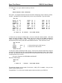
1
SBC6120 USER'S MANUAL Third Edition Copyright 2001-2003 by Spare Time Gizmos. Visit our web site at www.SpareTimeGizmos.com Permission is granted to copy, distribute and/or modify this document under the terms of the GNU Free Documentation License, Version 1.1 published by the Free Software Foundation; with no invariant sections; with the front cover text “Portions Copyright 2001-2003 by Spare Time Gizmos” and our URL, and with no back cover text. A copy of this license may be obtained from http://www.gnu.org/licenses/fdl.txt. CONTENTS 1 OVERVIEW ................................................................................................................................. 1 1.1 REGULATORY WARNING ...................................................................................................... 2 1.2 SAFETY WARNING ............................................................................................................... 2 1.3 WARRANTY ......................................................................................................................... 2 2 ASSEMBLY ................................................................................................................................. 3 2.1 ERRATA .............................................................................................................................. 3 2.2 PART SELECTION ................................................................................................................ 3 2.3 SOCKETS AND SOLDERING ................................................................................................... 4 2.4 ASSEMBLY HINTS ................................................................................................................ 6 2.5 FINAL CHECKOUT ................................................................................................................ 6 2.6 CONNECTORS ..................................................................................................................... 6 2.7 JUMPERS ............................................................................................................................ 9 2.8 TEST POINTS ...................................................................................................................... 9 3 HARDWARE DESCRIPTION ......................................................................................................... 11 3.1 PROCESSOR ..................................................................................................................... 11 3.2 MEMORY MANAGEMENT..................................................................................................... 12 3.3 CONSOLE TERMINAL .......................................................................................................... 13 3.4 RAM DISK ........................................................................................................................ 13 3.5 IDE INTERFACE ................................................................................................................. 14 3.6 POST CODE DISPLAY ....................................................................................................... 15 4 SOFTWARE DESCRIPTION ......................................................................................................... 17 4.1 POST............................................................................................................................... 17 4.2 RAM DISK SUPPORT ......................................................................................................... 18 4.3 ATA DISK SUPPORT .......................................................................................................... 18 4.4 OS/8 BOOTSTRAP ............................................................................................................. 20 4.5 LOADING OS/8 ONTO THE SBC6120.................................................................................. 21 5 COMMAND REFERENCE ............................................................................................................ 25 5.1 SPECIAL CHARACTERS ...................................................................................................... 25 5.2 MEMORY COMMANDS ........................................................................................................ 26 5.3 REGISTER COMMANDS ...................................................................................................... 29 5.4 BREAKPOINT COMMANDS ................................................................................................... 30 5.5 CONTROL COMMANDS ....................................................................................................... 31 5.6 TERMINAL COMMANDS ....................................................................................................... 32 5.7 LOAD/DUMP COMMANDS ................................................................................................... 33 5.8 IDE AND RAM DISK COMMANDS ........................................................................................ 33 5.9 MISCELLANEOUS COMMANDS............................................................................................. 36 5.10 ERROR MESSAGES ........................................................................................................ 36 6 ROM FUNCTION CALLS ............................................................................................................ 39 6.1 GET ROM VERSION .......................................................................................................... 39 6.2 READ/WRITE RAM DISK .................................................................................................... 39 6.3 GET RAM DISK SIZE ......................................................................................................... 40 6.4 GET RAM DISK BATTERY STATUS...................................................................................... 40 6.5 READ/WRITE IDE DISK ...................................................................................................... 40 6.6 GET IDE DISK SIZE ........................................................................................................... 41 6.7 SET IDE DISK PARTITION MAPPING .................................................................................... 41 6.8 GET IDE DISK PARTITION MAPPING ................................................................................... 41 6.9 COPY MEMORY ................................................................................................................. 41 6.10 COPY MEMORY EXTENDED............................................................................................. 42 6.11 LIGHTS .......................................................................................................................... 42 A. BUILDING OS/8 FOR THE SBC6120 ...................................................................................... 43 B. PARTS LIST .......................................................................................................................... 47 C. SILK SCREEN........................................................................................................................ 49 D. IOT REFERENCE ................................................................................................................... 51 Page i Spare Time Gizmos SBC6120 User's Manual 1 OVERVIEW The SBC6120 is a conventional single board computer with the typical complement of RAM, EPROM, and interfaces. What makes it unique is that the CPU is the Harris HD-6120 “PDP-8 on a chip.” Yes, a real PDP-8! The 6120 is the second generation of single chip PDP-8 compatible microprocessors, and was used in Digital’s DECmate-I, II, III and III+ “personal” computers. The SBC6120 can run all standard DEC paper tape software, such as FOCAL-69, with no changes what so ever. Simply use the ROM firmware on the SBC6120 to download FOCAL69.BIN from a PC connected to the console port (or use a real ASR-33 and read the real FOCAL-69 paper tape, if you’re so inclined!), start at 00200, and you’re running. OS/278, OS/78 and, yes - OS/8 V3D or V3S - can all booted and run on the SBC6120 using either RAM disk or IDE disk as mass storage devices. Since the console interface in the SBC6120 is KL8E compatible and does not use a HD-6121, there is no particular need to use OS/278 and real OS/8 V3D runs perfectly well. Of course, you must still avoid using the KT8A extensions in the OS/8 DEVEXT kit as the KT8A IOTs conflict with the 6120 stack instructions. Figure 1 – The SBC6120 4/22/2004 8:26 AM Page 1 Spare Time Gizmos 1.1 SBC6120 User's Manual REGULATORY WARNING In the United States, the Federal Communications Commission requires that devices that use and radiate radio frequency energy be certified in accordance with CFR Title 47, Parts 2 and 15. Other countries will have different requirements. The SBC6120 design is not in finished product form and has NOT been approved by the FCC or any other regulatory agency worldwide. The user understands that approvals may be required prior to the operation of the SBC6120, and agrees to utilize the SBC6120 in keeping with all laws governing its operation in the country of use. 1.2 SAFETY WARNING The RAMDISK board uses two Lithium coin cell batteries. There is a danger of explosion if this type of battery is incorrectly replaced. Replace with only the same or equivalent type recommended by the manufacturer. Dispose of used batteries only in accordance with the manufacturer's instructions. 1.3 WARRANTY SPARE TIME GIZMOS OFFERS NO WARRANTY, EXPRESS OR IMPLIED, AS TO THE RELIABILITY OR ACCURACY OF THE SBC6120 DESIGN. SPARE TIME GIZMOS OFFERS NO WARRANTY, EXPRESS OR IMPLIED, AS TO THE ACCURACY OF THE INFORMATION PRESENTED IN THIS DOCUMENT. SPARE TIME GIZMOS OFFERS NO WARRANTY, EXPRESS OR IMPLIED, AS TO THE SUITABILITY OR CORRECTNESS OF ANY SOFTWARE OR FIRMWARE SUPPLIED IN CONJUNCTION WITH THE SBC6120. SPARE TIME GIZMOS MAKES NO REPRESENTATIONS AS TO THE SUITABILITY OF THE SBC6120 FOR ANY APPLICATION. IT IS SOLELY AND EXCLUSIVELY YOUR RESPONSIBILITY TO EVALUATE THE ACCURACY, COMPLETENESS, AND USEFULNESS OF THE SBC6120 AND ALL RELATED DESIGNS, SOFTWARE, AND OTHER INFORMATION PROVIDED BY SPARE TIME GIZMOS. THE ENTIRE RISK AS TO THE USE AND PERFORMANCE OF THE SBC6120 IS ASSUMED SOLELY BY YOU. NO REPRESENTATION OR OTHER AFFIRMATION OF FACT, INCLUDING, BUT NOT LIMITED TO, STATEMENTS REGARDING CAPACITY, PERFORMANCE OF PRODUCTS, OR SUITABILITY FOR USE, WHETHER MADE BY SPARE TIME GIZMOS EMPLOYEES OR OTHERWISE, WILL BE DEEMED TO BE A WARRANTY FOR ANY PURPOSE, OR GIVE RISE TO ANY LIABILITY ON THE PART OF SPARE TIME GIZMOS. THE WARRANTIES AND CORRESPONDING REMEDIES AS STATED IN THIS SECTION ARE EXCLUSIVE AND IN LIEU OF ALL OTHERS, WRITTEN OR ORAL. SOME JURISDICTIONS DO NOT ALLOW THE EXCLUSION OF IMPLIED WARRANTIES, SO THE ABOVE EXCLUSION MAY NOT APPLY TO YOU. THE LIMITED WARRANTIES AND CONDITION REFERENCED ABOVE GIVE YOU SPECIFIC LEGAL RIGHTS. YOU MAY HAVE OTHERS, WHICH VARY FROM JURISDICTION TO JURISDICTION. IN NO EVENT SHALL SPARE TIME GIZMOS OR ITS EMPLOYEES BE LIABLE FOR ANY COSTS OR DIRECT, INDIRECT, PUNITIVE, INCIDENTAL, SPECIAL, CONSEQUENTIAL DAMAGES OR ANY OTHER DAMAGES WHATSOEVER INCLUDING, WITHOUT LIMITATION, DAMAGES FOR COSTS OF PROCUREMENT OF SUBSTITUTE GOODS OR SERVICES, LOST PROFITS, LOSS OF DATA, INTERRUPTION OF BUSINESS, OR LOSS OF USE, ARISING OUT OF OR IN ANY WAY CONNECTED WITH THE USE OR PERFORMANCE OF THE SBC6120 OR YOUR RELIANCE ON THE SBC6120 OR RESULTS FROM MISTAKES, OMISSIONS, INTERRUPTIONS, DELETION OF FILES, ERRORS, DEFECTS, DELAYS IN OPERATION OR TRANSMISSION, OR ANY FAILURE OF PERFORMANCE WHETHER BASED ON CONTRACT, TORT, STRICT LIABILITY OR OTHERWISE, EVEN IF SPARE TIME GIZMOS HAS BEEN ADVISED OF THE POSSIBILITY OF DAMAGES. BECAUSE SOME STATES/JURISDICTIONS DO NOT ALLOW THE EXCLUSION OR LIMITATION OF LIABILITY FOR CONSEQUENTIAL OR INCIDENTAL DAMAGES, THE ABOVE LIMITATION MAY NOT APPLY TO YOU. IN NO EVENT SHALL SPARE TIME GIZMOS' LIABILITY, IN THE AGGREGATE, EXCEED THE SUMS ACTUALLY PAID BY YOU TO SPARE TIME GIZMOS AND ACCEPTED BY SPARE TIME GIZMOS FOR THE USE OF THE SBC6120. 4/22/2004 8:26 AM Page 2 Spare Time Gizmos SBC6120 User's Manual 2 ASSEMBLY Many thanks to Steve Loboyko, Paul Schmidt, John Wren, Jim Kearney and the other SBC6120 builders who contributed their experiences and suggestions to this chapter. 2.1 ERRATA There are no known errors in Revision D of the SBC6120 board. 2.2 PART SELECTION The complete parts list for the SBC6120 is contained in Appendix B and, with the exception of the HD6120 CPU, all parts are common, modern, devices that should be readily available. Most part values are non-critical and substitutions should not be a problem, however when changing connectors or switches use care that the replacements will fit the footprint on the PC board. The SBC6120 is intended to use all CMOS devices. Be sure to use 74HC parts for all 74xx logic, CMOS 22V10 and 16V8 GALs, 27C64 or 27C256 CMOS EPROMs, and a CMOS 82C55 PPI. Be particularly careful of the latter, since NMOS 8255s are very common. 2.2.1 SRAMs The HM6208 SRAMs used in the SBC6120 were originally intended for use as cache memories with Intel 486 processors and are available in 25, 35 and 45 ns speeds. All of these are ridiculously fast by HD-6120 standards, and any version of the HM6208 may be used. 2.2.2 EPROMs Two EPROMs are used to hold the BTS6120 ROM monitor and bootstrap. Either 8K byte, 27C64 style, or 32K byte, 27C256 style, EPROMs may be used without any circuit changes or jumper settings, however be warned that not all 27C64 EPROMs will work in this circuit! Those which define Vpp as a “don’t care” during read will work fine, however those which require that Vpp be held at Vcc during reading will not work. In particular, AMD AM27C64 EPROMs work fine; National NM27C64 EPROMs do not. This problem applies only to 8K EPROMs – all makes of 32K 27C256 EPROMs should work without difficulty. 2.2.3 GALs Three GALs are used in the SBC6120 – two 22V10 types for IOT decoding and one 16V8 type for memory decoding. Atmel ATF22V10 and ATF16V8 parts were used in the SBC6120 prototype because these devices are flash memory based and may be erased and reprogrammed any number of times; however any GALs with the appropriate organization will work. 2.2.4 EconoReset The DS1233 EconoReset comes in two versions – one with a 5% Vcc tolerance and another with a 10% tolerance. The 10% version is recommended as the 5% version has a tendency to cause spurious RESETs whenever there is a slight drop in the Vcc. This situation is exacerbated by the picofuse, which has sufficient internal resistance to drop 0.2 to 0.3 volts at the 300mA draw of the SBC6120. It will be made worse if you are using a 2.5” laptop style hard disk, since these drives use +5V to power the motor. Even though the disk isn’t powered from the SBC6120, if you power both from the same supply it can cause a deep enough drop in Vcc to reset the DS1233 when the drive spins up. The 10% version of the DS1233 provides a wide enough tolerance to avoid these problems. 4/22/2004 8:26 AM Page 3 Spare Time Gizmos SBC6120 User's Manual 2.2.5 82C55 PPI You must use at least the 5 MHz version of the 82C55 (as indicated by an A5, or -5 suffix); slower parts will not work. 2.2.6 LED display Please be aware that the quad LED display specified for D2 has internal dropping resistors. Be sure you do not accidentally substitute a part without these resistors! 2.2.7 Fuse The picofuse (F1) and the zener diode (D1) are there to protect you against accidental over voltage or reverse polarity of the power supply. Yes, it will work without them, but they're cheap insurance1 and I strongly recommend you use them. If you decide to omit the fuse, remember that you must replace it with a wire jumper; you can’t simply leave it open! 2.2.8 Oscillators The SBC6120 uses two TTL oscillators, one to generate the baud rate clock for the console UART and another to generate the CPU clock. The baud rate generator, U23, must always be exactly 4.9152 MHz if we are to generate standard baud rates. U1 generates the CPU clock and should nominally be 5.0 MHz. These oscillators come in two versions – one with an ENABLE pin and one without – and either version may be used in the SBC6120. Harris specified the HD-6120 to work up to a maximum clock frequency of 5.1MHz, however DEC actually ran the DECmates at 8 MHz. Whether they were using specially selected parts or all 6120s would go this fast I have no way of knowing, but I have regularly run my SBC6120 at 8 MHz without problems. This can easily be changed by substituting an 8 MHz oscillator for U1. 2.3 SOCKETS AND SOLDERING Every kit that I have ever built, all the way from the legendary Heathkit2 on down, has always said that 90% of the kits that don’t work after they’re assembled fail because of the soldering. This is especially true of the SBC6120 – it is not an easy project to solder. The four layer PC board has internal power plans; this makes it difficult to solder power pins because the internal planes act as a heat sink and draw the heat away. The PC board was laid out with “8 and 8” design rules, which means that the traces are only 8 mils (that’s 0.008 inches!) wide and, in some places, there is only 8 mils of “air gap” between adjacent traces or pads. The SBC6120 is definitely not a “learn to solder” project – if you’ve never soldered a board like this before, then it’d be a good idea to find something cheaper to practice on! When it comes to soldering, having the proper tools makes all the difference. A temperature controlled soldering station with a 30 mil tip will can be purchased for about $100 and will make the job much more pleasant. The right solder is important too – “63/37” solder is preferable to the traditional “60/40” because it has a slightly lower melting point and requires less heat. You should not be using anything larger than 31 mil (0.031 inch) diameter solder. And finally, you’ll want a nice pair of wire cutters for trimming the leads on components after you’ve soldered them. Get the kind that’s made for trimming wires on PC boards – they have a special cutting face that cuts flush with the PC board without leaving any wire “stubs” sticking up. 1 On more than one occasion I have accidentally connected +12V to the +5 input on the SBC6120 and, although I wish I could say that I was just testing and I did it on purpose, in truth it was simple stupidity. I have blown several of the fuses but never fried a chip 2 Yes, I’m old enough to have built one or two. I missed their golden years, though. 4/22/2004 8:26 AM Page 4 Spare Time Gizmos SBC6120 User's Manual You’ll want to wash the bare PC board before you start soldering to remove any grease or oils from fingerprints. If you don’t wash them off, these oils will make the solder take longer to “flow” and will require more heat and flux to get a good solder joint. I prefer to use a mildly abrasive cleaner such as a Brillo pad, or Comet cleanser with a sponge, for cleaning. They do a better job removing oils, but remember to rub lightly – heavy scrubbing will remove the plating or the silkscreen! Lastly and most importantly, make sure the board is completely dry before you start soldering. Even a tiny amount of water left in a hole will turn to steam when soldering heat is applied and blow the solder right out of the hole! If you have it, compressed air or canned air is ideal for removing water from the holes and can be used to accelerate the drying process. Use care avoid solder bridges to adjacent traces and pads. There are a few pins where vias come up close to a pad and these are especially likely candidates for shorts. A few to watch out for are U18 pin 1, U16 pin 27, U15 pin 11, U13 pin 9, and there are several places inside J4. There are other places have traces running close to pins; some of these are U5 pin 35 to trace running below pin, U3 pin 1 to trace running above pin, and U18 pin 1 to trace to right of the pin. Some of the bypass caps are also very close to traces and, when you nip the leads on these, check that your cutters cut cleanly and don’t cause shorts. And finally, be careful not to use too much solder on the pins; excessive solder can “wick” up the pin to the top side of the board and cause invisible (because they’re hidden under the IC socket) shorts there. I strongly advise using good, high machined pin sockets for all ICs3. These sockets are admittedly expensive; a 16 pin DIP socket might cost 50 cents and a 40 pin DIP more than dollar, but they’re worth it if you ever need to replace an IC. Some people may object to the idea of putting a 25 cent 74HC74 IC into a 50 cent socket, but it’s not the IC you are protecting – it’s the PC board. If you ever fry that 74HC74 (and a single slip of the scope probe is all it takes!) then it will require significant skill and equipment to unsolder that dead IC without damaging the board. With a socket it takes only a few seconds to pop out the dead one a pop in a new one. The only possible exceptions to the “socket everything” rule are the two crystal oscillators. These may be socketed if you wish, but because of their height they will extend far above the other ICs and because of their metal cans they may short to any daughter boards mounted on the expansion connector. If you do decide to socket them, put a piece of electrical tape over them for insulation. When soldering IC sockets and connectors, especially the larger ones, start by holding the part tightly to the board and then soldering only two pins on diagonal corners. This will hold the part in place temporarily while you turn the board over and make sure the part is flush against the PC board. If it isn’t, then apply pressure to the part while using your iron to re-melt the solder on the closest pin. The worst thing is to solder all 40 pins on a connector only to turn it over and find that it’s all skewed. It’s pretty much impossible to desolder all those pins and repair the error at that point. Lastly, clean the board again after you’re finished soldering by using a commercial flux remover or, if you’ve used a solder with water soluble flux, by washing with a toothbrush and warm water. Some water soluble fluxes are corrosive in the long term and should not be left on the board. Traditional rosin fluxes won't actually hurt anything, but the residue obscures the traces and makes it harder to find shorts. Make sure everything is completely dry before you begin installing parts in the sockets; once again, compressed air can be used to accelerate the drying process. 3 Please don’t solder your only 6120 chip to the board! 4/22/2004 8:26 AM Page 5 Spare Time Gizmos 2.4 SBC6120 User's Manual ASSEMBLY HINTS Don’t install any ICs until you’ve read the next section, and when you do install the ICs notice that they are all oriented with pin one to the top or right, except IOT2 (U11, a 22V10). This one had to be oriented “backwards” to improve the trace routing. Many people have had difficulty getting the correct EPROM into the correct socket. It does no harm to reverse them, but it won’t work either! Remember that the PDP-8 numbers its bits “backward” from the usual convention, so the EPROM containing bits DX0..5 is the “HIGH” EPROM and bits DX6..11 are the “LOW” EPROM. In the silk screen (see Appendix C) U9, the one closest to the RESET push button, is the HIGH EPROM and U10 is the LOW, Seven 10K ohm resistors and one 4.7K resistor are used in the SBC6120; the lone 4.7K resistor is the one located between the UART and the IOT2 GAL. Don’t waste your time looking for R7 and R9 – they do not exist in this revision of the SBC6120. Twenty-two 0.1µF 50VDC monolithic bypass capacitors are used in the SBC6120. These are not identified in the silk screen, however their positions are shown in red in Appendix C. Capacitors C29, C30, C31 and C32 (1µF 25V tantalum) and C37 (47 1µF tantalum) are polarized devices and must be installed correctly. The polarization is shown on the silk screen of Revision E and later PC boards. 2.5 FINAL CHECKOUT After you finish assembly, apply power before installing any ICs. Check that the power LED lights; that +5 is present on the power pins of the IC sockets, and (if you soldered them in) that the oscillators are running. Next, install all the chips except the precious 6120 and measure the +5V current. It should be around 250mA - if it's more than 300mA, you have a problem somewhere that you should fix before risking your CPU. Lastly install the CPU, being careful to disconnect the power first and careful to take precautions against static damage to the 6120! Verify that you have set your baud rate correctly (refer to section 2.7.2); connect a terminal; apply power and you should see the LEDs count down in the binary sequence 7 6 5 .. 1. When the LEDs reach 1 you should see the BTS6120 sign on message: SBC6120 ROM Monitor V211 Checksum 3525 6642 12-JUN-01 19:50:01 Copyright (C) 1983-2001 Spare Time Gizmos. All rights reserved. RAM: 0KB - Battery FAIL IDE: Not detected The POST will pause for a moment on 4 - that's the memory test and it's normal for it to take a few seconds. Also note that the POST will fail on the console UART test (#2) if you've forgotten to install one of the baud rate jumpers (J11 .. J14). 2.6 CONNECTORS 2.6.1 Power J1 is the main power connector, and is compatible with a standard PC floppy/hard disk power cable. The following illustration shows the pin out of the power connector if you hold the SBC6120 board with the component side up and the rear connectors facing you. 4/22/2004 8:26 AM Page 6 Spare Time Gizmos SBC6120 User's Manual +12 VDC Ground Ground +5 VDC Figure 2 - Connector J1 Power consumption for the SBC6120 is less than one watt, approximately 175 mA at 5V. Fuse F1 and Zener diode D1 protect the SBC6120 from reverse polarity and over voltage on the +5V supply. The SBC6120 does not use +12V and it is unconnected on the board. WARNING! The power connector on the SBC6120 is “upside down” compared to the usual IDE disk drive. That is, +5 is on the outside of the PC board and +12 is on the inside. Do not attempt to force the plug in the wrong way! 2.6.2 IDE J2 is used to connect an IDE hard disk and, like J1, its configuration is compatible with the PC equivalent. A standard 40 pin IDE ribbon cable may be used to connect this connector to the hard disk. If a hard disk is not to be used with the SBC6120 then J2 may be used as a general purpose, twenty four bit, parallel I/O interface. Pins 1, 23, 25, 37 and 38 are inverted by the 74HC04 on the SBC6120 and can be used only as outputs, but the remaining pins may configured for either input or output by programming the 8255 PPI appropriately. Pin 1 3 5 7 9 11 13 15 17 19 21 23 25 27 29 31 33 35 37 39 Signal DRESET L DD7 DD6 DD5 DD4 DD3 DD2 DD1 DD0 GND N/C DIOW L DIOR L N/C N/C N/C DA1 DA0 CS1FX L DASP L4 PPI PC5 PB7 PB6 PB5 PB4 PB3 PB2 PB1 PB0 PC4 PC3 PC1 PC0 PC6 Pin 2 4 6 8 10 12 14 16 18 20 22 24 26 28 30 32 34 36 38 40 Signal GND DD8 DD9 DD10 DD11 DD12 DD13 DD14 DD15 N/C GND GND GND N/C GND N/C N/C DA2 CS3FX L GND PPI PA0 PA1 PA2 PA3 PA4 PA5 PA6 PA7 PC2 PC7 Table 1 - Connector J2 4 This signal is not connected to the PPI, however it may be tested by the SDASP (64118) IOT. 4/22/2004 8:26 AM Page 7 Spare Time Gizmos SBC6120 User's Manual 2.6.3 Console J3 is a ten pin header which connects to the console terminal and is intended to be used with a standard PC DB9 (or DB25, if you prefer) cable. Note that only TXD, RXD, and ground are connected. Pin 5 3 9 Signal TXD RXD GND Table 2 - Connector J3 J3 has exactly the same pin out as a PC, and therefore if you intended to connect the SBC6120 to a PC’s COM port you will want to use a null modem serial cable with female DB9 (or DB25) connectors on both ends. Be warned that there are actually two different types of serial cables used on PCs, and each type has a 10 pin IDC female header on one end and a DB9 on the other. One type, the “one-to-one” variety, is wired so that pin 1 of the header is connected to pin 1 of the DB9, pin 2 of the header to pin 2 of the DB9, and so on, up to pin 9 of the header connected to pin 9 of the DB9. This sounds like the logical way to do it, but it’s actually fairly awkward to wire this way using ribbon cable. Also, this is not the wiring that an IDC DB9 connector gives. The other way of wiring the cable, the “interleaved” way, has pin 1 of the header connected to pin 1 of the DB9, but pin 2 of the header connects to pin 6 of the DB9 (which is located below and between pins 1 and 2), pin 3 of the header connects to pin 2 of the DB9, pin 4 of the header connects to pin 7 of the DB9, and so on. This is the “natural” way to wire with ribbon cable and is also the wiring that an IDC type DB9 connector gives. The SBC6120 is intended to be used with this type of cable; the “one-to-one” type will give strange results. If you have any doubts about which type you have, pry off the shell of the DB9 and take a look – it’s pretty obvious upon inspection. 2.6.4 Expansion J4 is a general purpose expansion connector which can be used for the RAM disk daughter board or other I/O expansion options. If you design your own expansion board to fit this connector then use care to minimize loading since these signals are not buffered on the SBC6120. In particular, it would probably not be a good idea to connect a long ribbon cable to this connector! Pin 1 3 5 7 9 11 13 15 17 19 Signal VCC RD SR L SKIP L C0 L INTREQ L READ L WRITE L LOAD DAR H GND N/C Type PWR O5 OD6 OD OD O O O PWR Pin 2 4 6 8 10 12 14 16 18 20 Signal VCC WR SR L BYTE READ L C1 L INTGNT L IOCLR L LXDAR L DISK CE L GND N/C 5 Output (driven by the SBC6120). 6 Open drain input with a 10K pull up located on the SBC6120. 4/22/2004 8:26 AM Type PWR O OD OD O O O O PWR Page 8 Spare Time Gizmos Pin 21 23 25 27 29 31 33 35 37 39 41 43 45 47 49 Signal EMA2 MA4 MA5 MA6 MA7 MA8 MA9 EMA0 MA10 MA11 EMA1 DX5 DX6 DX7 GND SBC6120 User's Manual Type O O O O O O O O O O O B B B PWR Pin 22 24 26 28 30 32 34 36 38 40 42 44 46 48 50 Signal N/C N/C MA3 MA2 MA0 MA1 DX0 DX1 DX2 DX3 DX4 DX11 DX10 DX9 DX8 Type O O O O B7 B B B B B B B B Table 3 - Connector J4 2.7 JUMPERS 2.7.1 Break Enable J10 causes the 6120’s CPREQ input to be asserted whenever a framing error is detected on the console port. This allows you to break into the SBC6120 ROM monitor at any time simply by pressing the BREAK key on the console terminal. To disable this feature, remove J10. 2.7.2 Baud Rate Jumpers J11 through J14 select the console baud rate according to this table: Jumper J11 J12 J13 J14 Baud 38,400 9,600 1,200 300 Table 4 - Baud Rate Jumpers WARNING! Only one of these jumpers should be installed at any time! 2.8 TEST POINTS Test point TP1 is connected to RESET L. If you mount your SBC6120 in a box, you can connect this point to a second RESET push button on the front panel. The other side of the push button should be connected to ground. This test point can also be used with an EPROM emulator to allow the system to be reset when new code is downloaded. Test point TP3 is connected to ground and TP2 is connected to VCC (+5V). They are convenient places to connect the ground lead of your scope probe or the power leads of your logic probe. 7 Bi-directional (Tristate). 4/22/2004 8:26 AM Page 9 Spare Time Gizmos SBC6120 User's Manual 3 HARDWARE DESCRIPTION Besides the HD-6120 CPU, the SBC6120 has: ¾ 64KW (that's 64K twelve bit words) of RAM - 32KW for panel memory and 32KW for conventional memory. ¾ 8KW of EPROM which contains the BTS6120 firmware. Up to 32KW of EPROM can be supported by the SBC6120, however the firmware currently uses only 8K. ¾ Up to 2Mb (real eight bit bytes this time) of battery backed up, non-volatile SRAM which is bank switched and mapped into 6120 panel memory space. This memory is normally used as a RAM disk for OS/8, two megabytes being roughly equivalent to one RK05 disk pack! ¾ An elaborate memory management system that controls the mapping of RAM, EPROM and RAM disk into panel memory. ¾ A real, straight-8 compatible console terminal interface. The logic for this interface is implemented in a GAL - no 6121 is used and no software emulation is required8. ¾ An IDE/ATA disk interface implemented with an 8255 PPI and programmed I/O. ¾ Four LEDs, used to show POST error codes. Memory Map CPU 6120 RAM EPROM 64K x 12 8K x 12 Daughter Board RAM Disk 2M x 8 DAR MA[0:11], EMA[0:2] DX[0:11] UART POST Display 6402 PPI 8255 Console ATA Disk Figure 3 - SBC6120 Block Diagram 3.1 PROCESSOR The HD-6120 is a general purpose, high speed, CMOS 12 bit microprocessor designed to recognize the instruction set of Digital Equipment Corporation’s PDP-8/E minicomputer. Many 8 Mistakes that caused endless software compatibility problems in all models of the DECmate. 4/22/2004 8:26 AM Page 11 Spare Time Gizmos SBC6120 User's Manual architectural, functional and processing enhancements have been designed into the 6120 such that it can provide much higher system performance than its predecessor, the Intersil IM6100. The HD-6120 features include: ¾ ¾ ¾ ¾ ¾ A completely PDP-8/E compatible instruction set Built in KM8E compatible memory management A separate control panel memory for a bootstrap/monitor Two on-chip stack pointers A 2.75µs add cycle time with a 5.1MHz clock 3.2 MEMORY MANAGEMENT The SBC6120 has three memory subsystems - 64K words of twelve bit RAM, 8K words of 12 bit EPROM9, and up to 2Mb of 8 bit of SRAM with a battery backup for a RAM disk. The HD-6120 on the other hand, has only two memory spaces - panel memory and main memory, and each of these is limited to 32K words. The EPROM is a further problem because the PDP-8 instruction set makes it difficult, if not impossible, to get by without some read/write memory in every 4K field. The SBC6120 implements a simple memory mapping scheme to allow all three memory subsystems to fit in the available address space. The memory map in use is selected by four IOT instructions, MM0, MM1, MM2 and (what else?) MM3. Memory map changes take place immediately with the next instruction fetch - there's no delay until the next JMP the way there is with a CIF instruction. MM0 MM1 MM2 MM3 IOT 6400 6401 6402 6403 Function Select memory map 0 Select memory map 1 Select memory map 2 Select memory map 3 Table 5 - Memory Mapping IOTs The four memory maps implemented by the SBC6120 are: • Map 0 uses the EPROM for all direct memory accesses, including instruction fetch, and uses the RAM for all indirect memory accesses. This is the mapping mode selected by the hardware after power on or a reset. • Map 1 uses the RAM for all direct memory accesses, including instruction fetch, and uses the EPROM for all indirect memory references. This mode is the "complement" of map 0, and it's used by the ROM firmware initialization code to copy the EPROM contents to RAM. • Map 2 uses the RAM for all memory accesses and the EPROM is not used. This is the normal mapping mode used after the ROM firmware initialization. • Map 3 is the same as map 2, except that the RAM disk memory is enabled for all indirect accesses. RAM disk memory is only eight bits wide and reads and writes to this memory space only store and return the lower byte of a twelve bit word. This mode is used only while we're accessing the RAM disk. IMPORTANT! The memory mapping mode affects only HD-6120 control panel memory accesses. Main memory is always mapped to RAM regardless of the mapping mode selected. 9 The EPROM is actually 16 bits wide, but the hardware simply throws away the extra four bits. 4/22/2004 8:26 AM Page 12 Spare Time Gizmos 3.3 SBC6120 User's Manual CONSOLE TERMINAL The console terminal interface of the SBC6120 is software compatible with the traditional PDP-8 interface, and is a proper subset of the KL8E. The only difference between the SBC6120 and the KL8E are that the KCF, TFL, KIE and TSK10 instructions are omitted from the SBC6120. Console interrupts are permanently enabled, as they were in the original PDP-8. IOT KSF KCC KRS KRB TSF TCF TPC TLS 6031 6032 6034 6036 6041 6042 6044 6046 Function Skip if the console receive flag is set Clear the receive flag and AC OR AC with the receive buffer but don’t clear the flag Read the receive buffer into AC and clear the flag Skip if the console transmit flag is set Clear transmit flag, but not the AC Load AC into transmit buffer, but don't clear flag Load AC into transmit buffer and clear the flag Table 6 - Console Terminal IOTs The console interface in the SBC6120 does not use a 6121, and there'll be none of the “skip-onflag-and-clear-it” nonsense with KSF or TSF that plagued the DECmate family! If a daughter board is to be installed which will replace the standard PDP-8 console (e.g. a VT52 video terminal emulator), then SBC6120 onboard serial port must be disabled to prevent any conflicts. The SBC6120 implements two special IOTs which allow the device codes used by the onboard serial port to be changed. IOT SSLUCM 6412 SSLUSM 6413 Function Select SLU console mode (device codes 03/04) Select SLU secondary mode (device codes 36/37) Table 7 – Onboard Serial Port Mode IOTs Executing the SSLUSM IOT would cause the SBC6120 onboard serial port to respond to device codes 36/37 (e.g. KSF would become 6361; TLS would be 6476, etc), which allows an external device on the expansion bus to respond to the standard console 03/04 IOTs. Executing the SSLUCM IOT would return the onboard serial port to its normal console, 03/04, assignment. A normal program would ordinarily never worry about this – BTS6120 automatically detects, at startup, whether a secondary console device is present and configures the SBC6120 onboard serial port accordingly. The SSLUCM and SSLUSM IOTs were first implemented in revision B of the IOT2 PLD. The original version of the SBC6120 did not have these instructions; the onboard SLU device codes were fixed at 03/04. The software can easily determine which version of the PLD is installed by setting the AC to a non-zero value and then executing either SSLUCM or SSLUSM. On the original SBC6120 both these IOTs are NOPs which will leave the AC unchanged, however with the revision B PLD the AC will be cleared. 3.4 RAM DISK A daughter board is available which plugs into the SBC6120 expansion header and contains a DS1221 SRAM controller, one or two Lithium backup batteries and sockets for up to four, byte wide, low power CMOS SRAM chips. Each socket can contain a 512Kb SRAM, a 128Kb SRAM, 10 Or SPI, depending on which manual you read. 4/22/2004 8:26 AM Page 13 Spare Time Gizmos SBC6120 User's Manual or nothing. The maximum capacity of the RAM disk array is thus 2Mb - a respectably sized disk11 for OS/8. Figure 4 - RAM disk daughter board The SBC6120 maps these RAM chips into panel memory via the memory decode GAL and, when memory map 3 (see 3.2) is enabled, all indirect references to panel memory will access the RAM disk array. Since the RAM disk is only a byte wide, write operations discard the upper four bits of a twelve bit word, and when reading these bits are undefined and should be masked off by the software. Addressing the RAM disk is a little tricky, since a 2Mb memory requires a total of 21 address bits - quite a bit more than a PDP-8 can manage. RAM disk address bits 0..11 (the low order bits, contrary to the PDP-8 convention) are supplied by the HD-6120 MA11-0. The remaining 7 bits needed by each 512K SRAM come from a special register, the Disk Address Register, which can be loaded via the LDAR IOT. The final two bits needed by the DS1221 to select one of the four SRAM chips come from the HD-6120 EMA0 and EMA1 (EMA2 is not used at the moment). Put more simply, the data field selects the SRAM chip used, the DAR selects the 4K byte "bank" within the chip, and the normal memory address selects the individual byte within the bank. LDAR IOT 6410 Function Load RAM disk address register Table 8 - RAM Disk IOTs 3.5 IDE INTERFACE In the SBC6120 the IDE interface is implemented by a standard 8255 PPI, which gives us 24 bits of general purpose parallel I/O. PPI port A is connected the high byte (DD8..DD15) of the IDE data bus and port B is connected to the low byte (DD0..DD7). Port C supplies IDE control signals according to the following table. 11 Almost as big as a RK05J! 4/22/2004 8:26 AM Page 14 Spare Time Gizmos PPI C0..C2 C3 12 C4 12 C5 12 C6 12 C7 12 IDE DA0..2 DIOR DIOW RESET CS1Fx CS3Fx SBC6120 User's Manual Device address select I/O read I/O write Chip select for the 1Fx register space Chip select for the 3Fx register space Table 9 - IDE Control Signals One nice feature of the 8255 is that it allows bits in port C to be individually set or reset simply by writing the correct command word to the control register - it's not necessary to read the port, do an AND or OR, and write it back. We can use this feature to easily toggle the DIOR and DIOW lines with a single PWCR IOT. The HD-6120 can access the 8255 PPI by standard IOTs. PRPA PRPB PRPC PWPA PWPB PWPC PWCR IOT 6470 6471 6472 6474 6475 6476 6477 Function Read PPI Port A Read PPI Port B Read PPI Port C Write PPI Port A and clear the AC Write PPI Port B and clear the AC Write PPI Port C and clear the AC Write the PPI control register and clear the AC Table 10 - 8255 PPI IOTs 3.6 POST CODE DISPLAY The SBC6120 contains a row of four LEDs next to the RESET switch. The leftmost of these LEDs is a power indicator, and is always lighted as long as +5V is applied. The remaining three LEDs may be turned on and off by the software via the POST IOT, and are used to display the results of the Power On Self Test (see section 4.1). Power P0 P1 P2 Figure 5 - POST Code LEDs POST IOT 644n Function Display POST code n13 Table 11 - POST Display IOTs 12 These signals are inverted in the hardware so that writing a 1 bit to the register asserts the signal. 13 The POST bits are numbered according to the PDP-8 tradition so, for example, IOT 6444 would light LED P0. 4/22/2004 8:26 AM Page 15 Spare Time Gizmos SBC6120 User's Manual 4 SOFTWARE DESCRIPTION The 8KW EPROM contains the BTS6120 firmware, which has these features: ¾ A power on self test (POST) of the SBC6120 hardware, including the CPU, a memory test for EPROM, RAM and RAM disk, and a test of all peripheral devices. ¾ Commands to examine and change main memory or panel memory, plus commands to clear memory, move memory blocks, compute checksums, perform word searches, etc. ¾ Commands to examine and modify all 6120 registers. ¾ The ability to set break points in main memory programs, and to execute single instructions and generate instruction traces. ¾ A BIN format loader for loading paper tape images through the console port. ¾ RAM disk I/O functions to assist the OS/8 VM01 handler. ¾ IDE disk I/O functions to assist the OS/8 ID01 handler. ¾ Commands to upload and download both RAM and IDE disk over the serial port. ¾ An OS/8 bootstrap for both RAM and IDE disk. USER Applications OS/8 Keyboard Monitor Command Decoder VM01 Handler ID01 Handler Command Line Interpreter PR0 Function Calls Debugger BTS6120 Hardware Startup POST RAM Disk ATA Disk LEDs NV SRAMs 8255 PPI Upload Download Bootstrap Figure 6 - SBC6120 Software Architecture 4.1 POST If some part of the SBC6120 isn't working, say, for example, the RAM, BTS6120 would like to provide some diagnostic information before it ends up lost forever. The minimum set of system components that BTS6120 monitor needs to have working before it can print a prompt and execute commands is the CPU, the EPROM, the RAM, and the console terminal. The SBC6120 has a three bit LED display (see section 3.6) that can be set by the POST IOT. After power on or a reset BTS6120 tests each critical system component, and before each test it sets this LED display to a particular value. If that test fails and BTS6120 crashes or halts, the display remains at the last value set and indicates the cause of the failure. The POST codes and their associated failure modes are shown in Table 12. 4/22/2004 8:26 AM Page 17 Spare Time Gizmos P0 On On On On Off Off Off Off P1 On On Off Off On On Off Off P2 On Off On Off On Off On Off Code 7 6 5 4 3 2 1 0 SBC6120 User's Manual Failure CPU failure, or CPU is not a HD6120 Panel RAM bootstrap failure ROM checksum failure Memory test failure unused (reserved for future hardware) Console terminal failure Panel monitor (BTS6120) running (success!) Main memory program running Table 12 – POST Codes 4.2 RAM DISK SUPPORT As described in section 3.4, the SBC6120 RAM disk hardware divides the address space of each SRAM chip up into “banks” of 4K bytes. The BTS6120 firmware can fit 21 pages of 128 twelve bit words, packed using the standard OS/8 "three for two" scheme, into each 4K bank. A 512K SRAM chip holds 128 of these 4K banks, for a total capacity of 268810 PDP-8 pages or 134410 OS/8 blocks. A 128K SRAM would contain only 32 banks, for a total of 67210 PDP-8 pages or 33610 OS/8 blocks. Sixty-four bytes are wasted in each bank by this packing scheme, which works out to about 21 OS/8 blocks lost in each 512K SRAM. More clever software could reclaim these, but it would require that the three-for-two packing algorithm split PDP-8 pages across RAM disk banks. 4.2.1 VM01 Handler A standard OS/8 handler known as the VM01 is available for the SBC6120 RAM disk. Since the RAM disk can be mapped into panel memory space only, the VM01 handler uses the HD-6120 PR0 instruction to invoke BTS6120 functions that transfer data between RAM disk and main memory (see section 6.2). The VM01 handler implements four units, VMA0 through VMA3, corresponding to the four SRAM chips. The SRAM chips are completely independent, and if one or more are not installed then the corresponding VM01 units are simply treated as “off-line” and return I/O errors when accessed. By setting a conditional assembly switch, the VM01 handler may be built as a system, VMSY, or a non-system, VMNS, device. The system handler version of the VM01 contains a secondary bootstrap which can be booted by the BTS6120 B (BOOT) command (see section 5.8.3). 4.3 ATA DISK SUPPORT BTS6120 supports any standard ATA hard disk connected to the SBC6120 IDE interface. Nearly all hard disks with IDE interfaces are ATA; conversely, nearly all non-hard disk devices14 with IDE interfaces are actually ATAPI and not ATA. ATAPI requires a completely different protocol, which BTS6120 does not support, and BTS6120 will simply ignore any ATAPI devices connected to the IDE interface. BTS6120 supports only a single physical drive, which must be set up as the IDE master, and any IDE slave device will be ignored. Since BTS6120 does not support cylinder/head/sector (C/H/S) addressing, the hard disk used must support logical block addressing (LBA) instead. All modern IDE/ATA drives support LBA, as do most drives manufactured in the last five or six years, however some very old drives may not. If BTS6120 detects an ATA drive that does not support LBA it will display the message “IDE: Not supported” during startup and there after ignore the drive. 14 CD-ROMs, ZIP drives, LS120 drives, etc. 4/22/2004 8:26 AM Page 18 Spare Time Gizmos SBC6120 User's Manual All IDE devices, regardless of vintage, transfer data in sixteen bit words and each sector on an ATA disk contains 512 bytes, or 256 sixteen bit words. When writing to the disk, BTS6120 converts twelve bit PDP-8 words to sixteen bits by adding four extra zero bits to the left and, when reading from the disk, BTS6120 converts sixteen bit words to twelve bits by simply discarding the most significant four bits. No packing is done. This conveniently means that each ATA sector holds 256 PDP-8 words, or exactly one OS/8 block. It also means that one quarter of the disk space is wasted; in this era of multi-gigabyte disks that hardly seems like an issue. 4.3.1 Partitioning OS/8 handlers and the OS/8 file system use a single twelve bit word to hold block numbers, which means that OS/8 mass storage devices are limited to a maximum of 4096 blocks15. Using the BTS6120 non-packing scheme for storing data, 4096 PDP-8 blocks are exactly 2Mb. Clearly, if a single OS/8 device corresponds to an entire hard disk then nearly all of the disk space would be wasted. The normal solution is to partition the hard disk into many OS/8 units, with each unit representing only a part of the entire disk. Since OS/8 cannot support a single unit larger than 2Mb there isn’t any point in allowing partitions to be larger than that, and since the smallest drives available today can hold hundreds if not thousands of 2Mb partitions, there isn’t much point in allowing a partition to be smaller than that, either. Because of this, BTS6120 supports only fixed size partitions of 2Mb each. This greatly simplifies the software since a twenty four bit disk sector number can now be calculated simply by concatenating a twelve bit partition number with the twelve bit OS/8 relative block number (RBN). No “super block” with a partition table is needed to keep track of the sizes and positions of each partition, and the OS/8 handler is simplified since each disk partition is always the same size. A twenty four bit sector address permits disks of up to 8 GB to be fully used, which seems more than enough for a PDP-8. Once again, in BTS6120 the partition number simply refers to the most significant twelve bits of a twenty-four bit disk address, and the OS/8 block number is the least significant twelve bits. It’s no more complicated than that. 4.3.2 ID01 Handler The ID01 is the OS/8 handler for the SBC6120 IDE/ATA disk. It supports eight units, IDA0 through IDA7, in a single page and may be assembled as either a system (IDSY) or non-system (IDNS) handler. The system handler version of the ID01 contains a secondary bootstrap that can be booted by the BTS6120 Boot command (see section 5.8.3). The ID01 is a simple handler that uses HD-6120 PR0 instruction to invoke BTS6120 functions for low level IDE disk access and data transfer (see section 6.5). BTS6120 implements a partition map which defines the partition number corresponding to each OS/8 ID01 unit, and when an OS/8 program accesses an ID01 unit BTS6120 uses this table to determine the upper twelve bits of the LBA. At power on or after a MR command (section 0), BTS6120 initializes this partition map so that unit 0 accesses partition 0, unit 1 accesses partition 1, and so on up through unit 7 and partition 7. This mapping remains in effect until it is changed by either the PM command (section 5.8.5), or the Set IDE Disk Partition Mapping PR0 function (section 6.7). 4.3.3 OS/8 PART Program The largest mass storage device supported by OS/8 is actually only 4095 blocks, not 4096, and so the last block of every 2Mb partition is never used by OS/8. This block can, however, be accessed via the Read/Write IDE disk PR0 function (section 6.5), and it can be used to store the 15 More correctly, the actual OS/8 limit is 4095 blocks, but there’ll be more on that later. 4/22/2004 8:26 AM Page 19 Spare Time Gizmos SBC6120 User's Manual name, creation date, and other information about that partition. The OS/8 PART program uses this to allow partitions to be mounted on ID01 logical units by name rather than partition number. Named partitions are strictly a function of the OS/8 PART program and BTS6120 knows nothing about them. 4.4 OS/8 BOOTSTRAP BTS6120 contains a primary bootstrap for both the RAM disk and IDE disk devices, and the OS/8 handlers for these devices, VM01 and ID01, contain a secondary bootstrap for OS/8. There is lots of documentation on how to write a device handler, even a system handler, for OS/8 but a description of how to make a bootable device is not easy to find. Here’s a brief summary: • The primary bootstrap for a device16 normally loads cylinder 0, head 0, sector 0 (which is the equivalent to OS/8 logical block zero) into memory page zero field zero. This contains the secondary bootstrap which is then started in some device specific way; usually the primary bootstrap is overwritten by this data and the CPU just "ends up" there. • The secondary bootstrap is defined in the header of the system device handler and OS/8 BUILD copies this code from the handler to block zero when it builds the system device. The second half of block zero contains the system handler (that is, what's resident in page 7600 while OS/8 is running), plus some device independent OS/8 resident code that BUILD wraps around it. All of the second half of block zero must be loaded into page 7600, field 0 by the secondary bootstrap. • The remainder of the first half of block zero, the part after the secondary bootstrap, contains the OS/8 resident code for field 1. This starts at offset 478 and needs to be loaded into the corresponding locations of page 7600, field 1. The remaining words in page 7600, field 1 (i.e. those that occupy the same space as the secondary bootstrap) are used by OS/8 for tables and their initial values are unimportant. Most devices simply copy the entire first half of block zero to page 7600, field 1. • All this discussion presupposes a single page system handler, as we have for both the VM01 and ID01. For a two page system handler BUILD will put the second handler page in the first half of block 66 and the secondary bootstrap is also responsible for moving it from here into memory page 7600, field 2. • Once everything has been loaded, the secondary bootstrap can simply jump to location 7600, field 0, to load the OS/8 keyboard monitor. 4.4.1 ID01 and VM01 Primary Bootstrap The primary bootstrap for the SBC6120 RAM and IDE disks are six words loaded in locations 0 through 5: 0000/ 0001/ 0002/ 0003/ 0004/ 0005/ 6206 0001 0100 0000 0000 7402 PR0 1 0100 0000 0000 HLT / execute a panel request / 1 for RAM disk, 4 for IDE disk / read one page into field zero / location zero / from page/block zero of the device / should never get here If all goes well, the HLT in location 5 is never executed - it is over written by the secondary bootstrap code before BTS6120 returns from the PR0 function. Either device can be booted by depositing these six instructions in main memory with the D command (section 5.2.3) and then 16 The one which you have to toggle in with the switches! 4/22/2004 8:26 AM Page 20 Spare Time Gizmos SBC6120 User's Manual starting at location zero with the ST command (section 5.5.1), but it normally such heroics are not necessary. The SBC6120 B command (section 5.8.3) does the same job with much less work. 4.4.2 Boot Key The B (section 5.8.3) command in BTS6120 actually bypasses the primary bootstrap step and simply reads block zero of the boot device into page zero, field zero directly. The VM01 and ID01 secondary bootstraps all contain a special "key" in words 0 through 5, the ones which would normally overwrite the primary bootstrap, and BTS6120 looks for this key to identify a bootable volume. If the key is found, then BTS6120 simply jumps to main memory location 5 to start the secondary bootstrap and finish loading OS/8. This system should also work for any other, non-OS/8, system provided that it uses the same primary bootstrap shown above and that its secondary boot contains the special key in the first five words. As long as the secondary bootstrap starts at offset 5, the remainder of its code is unimportant to BTS6120 and it can do anything it likes. What’s the magic key? The letters “BOOT”, in eight bit ASCII one character per word, in locations 0 to 4, and a zero in location 5. 4.5 LOADING OS/8 ONTO THE SBC6120 Now that you've built your SBC6120 you're probably wondering how to get OS/8 loaded on it. After all, you can't very well put in your RX01 floppy or your RK05 disk pack and boot it up. There are at least four ways to get OS/8 onto the SBC6120: ¾ Use a PC to build an IDE disk with a bootable OS/8 image on it ¾ Download a bootable OS/8 image to the SBC6120 over the serial port ¾ Program an EPROM for the RAM disk board with a bootable OS/8 image ¾ Use the BTS6120 BU (Build) command to build bootable media All of these options will require that you have some form of PDP-8 emulator running on a PC. The emulator must be able to run OS/8 and it must support emulation of the SBC6120 ID01 IDE and/or VM01 RAM disk devices. Not surprisingly, the Spare Time Gizmos WinEight emulator fills all these requirements nicely. Other emulators, such as Bob Supnik's, could undoubtedly be used if someone is willing to write the necessary code for ID01 and VM01 emulation. The general plan is to use the emulator to boot OS/8 from standard media (e.g. RX01, RK05, RL01, etc.), load and compile the SBC6120 ID01 and VM01 device drivers, and then use the OS/8 BUILD program to build a bootable IDE or RAM disk image file. If you have no idea how to go about using BUILD to configure an OS/8 system, then you should read Appendix A for a brief summary of the procedure. Once you have a bootable ID01 or VM01 image, you can use the emulator to transfer whatever OS/8 CUSPS you like from your OS/8 system to the SBC6120 boot image. After that, the only tricky part is to transfer the RAM disk or IDE disk image from your PC to the SBC6120. NOTE The copyright for OS/8 is still held by Digital Equipment Corporation17 and Spare Time Gizmos cannot supply OS/8 software for your SBC6120. DEC has kindly granted permission to use OS/8 on Bob Supnik's PDP-8 emulator, however the legal status of using OS/8 on home built hardware is uncertain. 17 subsequently Compaq Computer, and subsequently to that, Hewlett-Packard. 4/22/2004 8:26 AM Page 21 Spare Time Gizmos SBC6120 User's Manual That said, it isn't hard to find copies of OS/8 on the Internet, and a little surfing should lead you to what you need. 4.5.1 Building a bootable IDE disk on the PC Once you've built a bootable OS/8 ID01 disk image file on your PC, you can take your SBC6120's IDE disk and physically connect it to the PC, and then use the MKID01 program to transfer the image file to the disk. Most likely you will want to connect your SBC6120's IDE disk to the PC as a slave drive since you'll still want another master IDE disk containing Windows (or at least DOS) for booting the PC. It's conceivable that the SBC6120's disk could be the only IDE disk on the PC and the PC booted from either a floppy or a SCSI disk, but that's left as an exercise for the reader. After you've temporarily connected the SBC6120's IDE disk to a PC, you can use the MKID01 program to write an ID01 disk image from the PDP-8 emulator to the physical drive. For example: MKID01 -u1 -w0 os8.id1 The -u1 option tells MKID01 to use IDE unit #1 (the primary slave) as the target drive, -w0 instructs it to write SBC6120 partition 0, and os8.id1 is the name of the ID01 image file from the emulator. The PDP-8 emulator must write the image file in exactly the same format that the SBC6120 uses (WinEight does) as MKID01 simply copies the entire file, verbatim, to the IDE disk. The Spare Time Gizmos FLX8 program is also able access a physical IDE disk in the SBC6120 OS/8 format, and it knows how to transfer files between DOS and OS/8 file systems. If you have other files you want to copy to your SBC6120 (source files, games, whatever!), now is a convenient time to use FLX8 to initialize one or more other partitions on the SBC6120's IDE disk and load them with files from the PC. You can now disconnect the IDE disk from your PC and reconnect it to the SBC6120. If you changed the disk to a slave drive be sure to change it back to a master before reconnecting it, since BTS6120 will not recognize a slave drive. If all is well you should be able to power up the SBC6120 and use the B ID command to boot OS/8 from the IDE disk. 4.5.2 Download a bootable OS/8 image over the serial port It is also possible to take an ID01 or VM01 image file on the PC, convert it to ASCII text, and then download that text to the SBC6120 over the console serial port. The BTS6120 firmware contains two commands, RL and DL, for just this purpose. The disadvantage to this scheme, naturally, is that it is slow. An image of a 512kb RAM disk requires approximately 2199k bytes in ASCII and takes about forty-five minutes to download; an IDE disk partition would take about three hours. The MKDLTXT program will convert either a VM01 or ID01 disk image to ASCII text in a format suitable for BTS6120. For example: MKDLTXT system.vm1 >system.txt will convert the file VM01 image system.vm1 to ASCII text and write the result to standard output, which is redirected to the file system.txt. The same command is used to convert an ID01 image to text - MKDLTXT automatically determines the input type by the file extension. The converted text files include a checksum for each disk block which BTS6120 uses to guard against transmission errors, however BTS6120 does not implement any special protocol or handshaking (e.g. X-Modem or Kermit) for transferring the text. The PC software must be careful, therefore, not to send data faster than the SBC6120 can process it. BTS6120 prompts for each new record with a ":" character, and the PC terminal emulation software should wait for this prompt before transmitting each line. 4/22/2004 8:26 AM Page 22 Spare Time Gizmos SBC6120 User's Manual The typical Kermit commands used to download a disk image to the SBC6120 are: set port com1 set modem type direct set baud 9600 set flow none set handshake none set carrier-watch off set file type text set transmit prompt 58 transmit system.txt Other PC communications programs will no doubt work equally well; it's just a matter of figuring out the appropriate settings for your favorite one. 4.5.3 Program an EPROM for the RAM disk board The SBC6120 RAM disk daughter board will allow either a 27C010 (128k x 8) or 27C040 (512k x 8) EPROM to be used in place of any SRAM chip, and the BTS6120 firmware simply treats the corresponding OS/8 VM01 device as "write protected". BTS6120 contains some special processing in the VM01 assist firmware which allows OS/8 to run from a write protected system device by using spare panel RAM to store system scratch blocks. Programming an EPROM for the SBC6120 RAM disk couldn't be easier - the VM01 image files produced by the WinEight emulator are exact images of what the real SBC6120 and BTS6120 would store in a SRAM chip. You can simply take a .VM1 file and program it, byte-for-byte, into a suitable EPROM. No preprocessing is necessary. 4.5.4 Use the BTS6120 BU (Build) The SBC6120 contains 32K twelve-bit words of EPROM to store the BTS6120 firmware, however BTS6120 actually uses only 8K of this. The remaining 24K words can be used to hold two very abbreviated OS/8 system images, one for RAM disk and the other for IDE disk. The BTS6120 BU command uses these images to build a bootable system on either type device. Because of the limited space available, only the OS/8 system head can be stored in the SBC6120 EPROM. No CUSPS or other programs fit in the EPROM, and an OS/8 system built this way will have an empty directory for SYS. This is just the absolute minimum amount necessary to have OS/8 boot, print a ".", and nothing more - probably it's not too useful in the real world! Because of copyright concerns, the SBC6120 EPROMs supplied by Spare Time Gizmos contain only BTS6120 and DO NOT contain any OS/8 boot images. If you want to use this feature on your SBC6120, you'll have to build your own EPROMs. To do this, you'll first need to build bootable images for both VM01 and ID01 devices. Remember that only the OS/8 system head is preserved by this process, so only the OS/8 kernel itself and the device handlers matter. Don't waste time loading any CUSPs or other files on to either image, because they will simply be lost. The MKSBCROM program is used to combine the BTS6120 firmware with the two disk images. The result is two .HEX files, one for the high order six bits and the other for the low six bits, which can be programmed into two 27C256 EPROMs and then installed on the SBC6120. MKSBCROM high.hex low.hex bts6120.bin [system.id1 system.vm1] 4/22/2004 8:26 AM Page 23 Spare Time Gizmos SBC6120 User's Manual 5 COMMAND REFERENCE A large part of BTS6120 is a user interface with an extensive set of commands for poking through memory and registers, setting break points, uploading and downloading memory and disk images over the console serial port, and booting an operating system. BTS6120 commands consist of a one or two letter command, possibly followed by some arguments. In most cases some or all arguments are optional and will have appropriate default values if they are not specified. BTS6120 is case insensitive and both commands and arguments may be given in either upper or lower case. BTS6120 commands that access memory will accept either full fifteen bit, 5 octal digit, addresses that include a field, or twelve bit, 4 octal digit, addresses without the field. If a twelve bit address is used then the command will always apply a default field value. Usually the default field will be the data field from the main memory program’s PS register, but a few commands that implicitly reference code (e.g. the BP command) will use the instruction field instead. Generally this is useful, however occasionally it can lead to unexpected results18 and it’s always safest to give a full, five digit, address. 5.1 SPECIAL CHARACTERS 5.1.1 Command Editing Control Characters While entering commands, BTS6120 recognizes several control characters for command editing: CHARACTER Control-H (Backspace) RUBOUT (Delete) Control-R Control-U Control-M (Return) FUNCTION Delete the last character entered (echoes as backspace, space, backspace). Delete the last character entered (echoes the character deleted) Retype the current command line, including all corrections. Cancel the current command line and start another Ends entry of the current command and starts interpreting it Table 13 - Command Editing Control Characters 5.1.2 Output Control Characters BTS6120 recognizes three special characters to control terminal output: CHARACTER Control-S (XOFF) Control-Q (XON) Control-O FUNCTION Suspend output until an XON is received Resume output after an XOFF Suppress output (acts as a toggle) Table 14 - Output Control Characters 5.1.3 Control-C The Control-C character may be used at any time to interrupt the current command and return to the BTS6120 prompt. 18 For example, “E 1234” and “E 01234” don’t necessary refer to the same location! 4/22/2004 8:26 AM Page 25 Spare Time Gizmos SBC6120 User's Manual 5.1.4 BREAK If jumper J10 is installed (see 2.7.1) then a framing error on the console port, caused when the terminal sends a BREAK, will immediately enter control panel mode. SBC6120 will print a message similar to this one: %Break at 01211 PC>1211 PS>5000 AC>0000 MQ>0000 SP1>0000 SP2>0000 > If you pressed BREAK by accident, you can usually use the C command to continue at this point and no harm will be done. 5.1.5 ; (Command Separator) The semicolon, “;”, character may be used as a separator between multiple commands on the same line. Format >aa; bb; cc; dd [; …] 5.1.6 ! (Comment) The exclamation, “!”, may be used as a comment character. Any text after the exclamation up to the end of the line is ignored. Format >!any text… 5.2 MEMORY COMMANDS 5.2.1 E (Examine Main Memory) The E command allows the user to examine the contents of main memory in octal, either one word at a time or an entire range of addresses at once. In the latter case, a memory dump is printed with eight PDP-8 words per line. Formats >E >E >E >E faaaa aaaa aaaaa-bbbbb aaaaa, bbbbb, ccccc, … ⇒ examine location aaaa, field f. ⇒ examine location aaaa of the current data field ⇒ examine locations aaaaa to bbbbb ⇒ examine several memory locations at once Examples >E 1234 31234/ 3145 >E 01234 01234/ 2213 >E 71000-72000 71000/ 7602 7105 6040 5100 1500 7777 7657 1777 … output deleted … 71770/ 7170 1717 7172 1737 7147 7715 7671 7177 72000/ 0200 2010 0202 2030 0240 0025 0602 0207 4/22/2004 8:26 AM Page 26 Spare Time Gizmos SBC6120 User's Manual 5.2.2 EP (Examine Panel Memory) The EP command is identical to E, except that panel memory is examined rather than main memory. 5.2.3 D (Deposit Main Memory) The D command allows the user to deposit one or more words in memory. The first argument specifies the memory address to be modified and the second argument is the value to be stored. Any number of values may be deposited into consecutive locations if they are separated by commas. Formats >D aaaa bbbb >D faaaa bbbb >D faaaa bbbb, cccc, dddd, … ⇒ deposit bbbb in location aaaa of the current data field ⇒ deposit bbbb in location aaaa, field f ⇒ deposit numbers bbbb, cccc, dddd, etc. in consecutive memory locations starting at faaaa Examples >D 0123 4567; E 0123 60123/ 4567 >D 40000 1,2,3,4 >E 40000-40007 40000/ 0001 0002 0003 0004 7704 0705 4371 6607 5.2.4 DP (Deposit Panel Memory) The DP command is identical to D, except that panel memory is changed rather than main memory. WARNING! There is no protection against corrupting BTS6120 when using this command! 5.2.5 BM (Block Move Memory) The BM command is used to move blocks of memory words from one location to another. It has three parameters - the source address range (two 15 bit numbers), and the destination address (a single 15 bit number). All words from the starting source address to the ending source address are transferred to the corresponding words starting at the destination address. Transfers may cross a field boundary and any number of fields may be copied at one time. This command operates only on main memory and there is no corresponding block move command for panel memory! Format >BM aaaaa-bbbbb ddddd ⇒ move the block of memory from addresses aaaaa to bbbbb to the block starting at address ddddd Examples >BM 00000-37777 40000 ! copy fields 0 through 3 to fields 4 through 7 >BM 0-7777 10000 ! copy all of field 0 to field 1 >BM 200-377 400 ! copy page 1 in the current data field to page 2 4/22/2004 8:26 AM Page 27 Spare Time Gizmos SBC6120 User's Manual 5.2.6 CK (Checksum Memory) This command will compute the checksum of all memory locations between the two addresses specified and the resulting twelve bit value is then printed on the terminal. This is useful for testing memory, comparing blocks of memory, and so on. The checksum algorithm used rotates the accumulator one bit between each word, so blocks of memory with identical contents in different orders will give different results. This command operates only on main memory and there is no corresponding command for panel memory. Format >CK aaaaa-bbbbb ⇒ checksum locations aaaaa through bbbbb Example >CK 10000-10177 Checksum = 0135 ! checksum all of page 0, field 1 5.2.7 WS (Word Search Memory) The WS command searches memory for a specific bit pattern. It accepts up to 4 operands: (1) the value to search for, (2) the starting search address,(3) the final search address, and (4) a search mask. All values except the first are optional and have appropriate defaults. Any location in the specified range that matches the given value after being masked is typed out along with its address. This command operates only on main memory and there is no equivalent for panel memory. Formats >WS vvvv >WS vvvv aaaaa-bbbbb >WS vvvv aaaaa-bbbbb mmmm Examples >WS 6031 01045/ 6031 01207/ 6031 >WS 6031 30000-33777 ?Search fails ⇒ search all of memory for the word vvvv ⇒ search for vvvv between aaaaa and bbbbb ⇒ search for the word vvvv between locations aaaaa and bbbbb using mmmm as search mask ! search all of memory for KSF instructions ! search words 0..3377 of field 3 for KSFs >WS 6030 0-77777 7770 ! search memory for any keyboard IOTs 01042/ 6034 01045/ 6031 01106/ 6032 01207/ 6031 01212/ 6034 01214/ 6032 07616/ 6034 07621/ 6031 5.2.8 FM (Fill Memory) The FM command fills a range of memory locations with a constant. This command operates only on main memory and there is no corresponding command for panel memory. Formats >FM vvvv 4/22/2004 8:26 AM ⇒ fill all of memory with the constant vvvv Page 28 Spare Time Gizmos SBC6120 User's Manual >FM vvvv aaaaa-bbbbb ⇒ fill all locations from aaaaa to bbbbb with vvvv Examples >FM 7402 0-7777 ! fill all of field zero with HLT instructions >E 1000-1001 01000/ 7402 7402 7402 7402 7402 7402 7402 7402 >FM 7777 0-77777 ! fill all of memory with –1 >E 11000-11007 11000/ 7777 7777 7777 7777 7777 7777 7777 7777 5.2.9 CM (Clear Memory) Th CM command will clear a block of memory. exception that the fill value is always zero. It is identical to the FM command with the Formats >CM >CM aaaaa-bbbbb Example >CM >CK 0-77777 Checksum = 0000 5.3 ⇒ clear all of memory ⇒ clear all locations from aaaaa to bbbbb ! clear all of memory REGISTER COMMANDS 5.3.1 ER (Examine Register) The ER command examines either a single register, when the register name is given as an argument, or all registers when no argument is given. Remember that this command is really examining the state of the main memory program that was saved when panel mode was last entered, and not the actual contents of the BTS6120 registers now. Formats >ER xx >ER ⇒ print register xx - xx can be AC, MQ, PC, SR, or PS ⇒ print all registers Examples >ER PC PC>1211 >ER PC>1211 PS>5000 AC>0000 MQ>0000 SP1>0000 SP2>0000 5.3.2 DR (Deposit Register) The DR command deposits a value in a register, and both a register name and an octal value are required arguments. Like the ER command, this is really changing the saved state of the main memory program and not the current BTS6120 registers. Any register values set with this command will be used after the next P, C, TR or SI command. 4/22/2004 8:26 AM Page 29 Spare Time Gizmos SBC6120 User's Manual Format ⇒ deposit yyyy into register xx >DR xx yyyy 5.4 BREAKPOINT COMMANDS 5.4.1 BL (List Breakpoints) This command will list all the breakpoints that are currently set. It has no operands. Format ⇒ list all the currently set breakpoints >BL 5.4.2 BP (Break Point) The BP command sets a breakpoint in the main memory program. It requires a single argument giving the 15 bit address where the breakpoint is to be set. WARNING! It is not possible to set a breakpoint at location zero in any field. BTS6120 uses zero as a marker for an unused breakpoint table entry. Formats >BP faaaa >BP aaaa ⇒ set a breakpoint at location faaaa ⇒ set breakpoint at aaaa in the current instruction field Examples >BP 07605 ! set a breakpoint at location 7605, field 0 >BP 7605 ! IF = 1 >BL 07605/ 0000 17605/ 0000 5.4.3 BR (Remove Breakpoint) The BR command removes a breakpoint at a specific address or, if no argument is given, removes all breakpoints. Formats >BR >BR aaaaa ⇒ remove all breakpoints ⇒ remove only the breakpoint at location aaaaa Examples >BR 17605 ! remove the breakpoint at location 7605, field 1 >BL 07605/ 0000 >BR >BL ?None set ! remove all breakpoints regardless of address 5.4.4 P (Proceed) The P command is used to proceed after the main memory program has stopped at a breakpoint. You can't simply continue at this point because the PC points to the location of the breakpoint, 4/22/2004 8:26 AM Page 30 Spare Time Gizmos SBC6120 User's Manual and the C (Continue) command would simply break again, instantly. The P (Proceed) command gets around this problem by first executing a single instruction, and then continuing normally. Format ⇒ proceed past a breakpoint >P 5.5 CONTROL COMMANDS 5.5.1 ST (Start) The start command initializes the CPU registers and all I/O devices and then transfers control to a main memory program. A single, optional, argument may be given to specify the start address of the main memory program. If the start address is omitted, then the default is location 7777 of field 0 (this is a little strange by PDP-8 standards, but it's the typical reset vector for 6100 and 6120 devices). Formats >ST >ST aaaaa ⇒ start the program at location 77777 ⇒ start the program at location aaaaa 5.5.2 C (Continue) The C command will restore all saved main memory registers and resume execution of the main memory program at the location indicated by the PC. Format ⇒ restore the main memory registers and continue >C 5.5.3 SI (Single Instruction) The SI command will execute a single instruction of the main memory program and then return control to BTS6120. It is the same as the TR command, except that no registers are printed. Format >SI ⇒ execute a single instruction with no register printout Example >RP 3; SI; E 10 00010/ 2222 00010/ 2223 00010/ 2224 ! single step 3 times and watch location 10 change 5.5.4 TR (Trace) The TR command will execute one instruction of the main memory program and then print the registers. It always executes one instruction, but it may be combined with the RP command to execute multiple instructions. Format >TR ⇒ execute a single instruction, then print the instruction and registers 4/22/2004 8:26 AM Page 31 Spare Time Gizmos Example >RP 10; IR>1123 IR>6034 IR>3034 IR>6032 IR>4322 IR>1722 IR>2322 IR>7450 IR>1034 IR>7650 SBC6120 User's Manual TR ! execute 10 instructions and watch the registers PC>1212 PS>5000 AC>0200 MQ>0000 SP1>0000 SP2>0000 PC>1213 PS>4000 AC>0215 MQ>0000 SP1>0000 SP2>0000 PC>1214 PS>4000 AC>0000 MQ>0000 SP1>0000 SP2>0000 PC>1215 PS>4000 AC>0000 MQ>0000 SP1>0000 SP2>0000 PC>1323 PS>4000 AC>0000 MQ>0000 SP1>0000 SP2>0000 PC>1324 PS>4000 AC>7553 MQ>0000 SP1>0000 SP2>0000 PC>1325 PS>4000 AC>7553 MQ>0000 SP1>0000 SP2>0000 PC>1327 PS>4000 AC>7553 MQ>0000 SP1>0000 SP2>0000 PC>1330 PS>4000 AC>7770 MQ>0000 SP1>0000 SP2>0000 PC>1332 PS>4000 AC>0000 MQ>0000 SP1>0000 SP2>0000 5.5.5 EX (Execute IOT) The EX command allows a user to type in and execute an IOT instruction directly from the terminal, which can be very useful for testing peripheral devices. The first argument is the octal code of the IOT to be executed, and the second (which is optional) is a value to be placed in the AC before the IOT is executed. If it is omitted, zero is placed in the AC. After the instruction is executed, the word SKIP is typed if the instruction skipped, along with the new contents of the AC. WARNING! Some care must be exercised with this command, since executing the wrong IOT can crash BTS6120! Formats >EX 6xxx >EX 6xxx yyyy ⇒ execute IOT 6xxx instruction and print the results ⇒ put yyyy in the AC and then execute IOT 6xxx Examples >EX 6471 AC>0002 ! execute IOT 6741 >EX 6474 1176 Skip AC>0000 ! put 1176 in the AC and execute IOT 6474 5.5.6 MR (Master Reset) The MR command executes a CAF instruction which asserts IOCLR L and initializes all external I/O devices. It then it resets the saved state of the main memory program to the default values, re-initializes the IDE disk and finally resets the disk partition map. From the point of view of an I/O device or a main memory program, this is equivalent to pressing the RESET button. This command does not have any effect on the contents of main memory. Format >MR ⇒ perform a master reset 5.6 TERMINAL COMMANDS 5.6.1 TW (Terminal Width) The TW command sets the terminal screen width to the value of its argument, which is a decimal number and must be in the range 32 to 255. BTS6120 will generate an automatic carriage return whenever an input or output line reaches the screen width. 4/22/2004 8:26 AM Page 32 Spare Time Gizmos SBC6120 User's Manual Format >TW nn ⇒ set the terminal width to nn (decimal) 5.6.2 TP (Terminal Page) The TP command sets the terminal page size to the value of its argument, in decimal, which must be in the range 12 to 48, or zero. BTS6120 will automatically pause terminal output whenever the specified number of lines is reached; output will resume when the user presses Control-Q (see section 5.1.2). A page size of zero disables the automatic XOFF function. Format >TP nn 5.7 ⇒ set the console screen size to nn (decimal) LOAD/DUMP COMMANDS 5.7.1 LP (Load Paper tape) The LP command loads a "paper tape" from the console terminal in standard PDP-8 BIN loader format. If your console is actually an ASR-33 and you have a real PDP-8 paper tape then this will probably even work, but a more likely situation is that you're using a PC with a terminal emulator and in that case the paper tape image can be downloaded from the PC's disk. The loader accepts all standard BIN data frames, including field changes, and correctly calculates and verifies the tape checksum. If the checksum matches then the number of words loaded is printed, but otherwise a checksum error message is generated. When initially started, this command ignores all input until two consecutive leader codes (octal 200) are found, which allows us to ignore any extra ASCII characters from the terminal emulator (such as carriage returns, spaces, etc). Since we're using the real console, the same one that you're typing commands on, for input we have a problem in that we need some way to terminate loading. Control-C won't work since the BIN loader eats all eight bit characters. A hardware reset isn't a good idea, since the POST memory test will erase everything we've loaded. Instead, the BIN loader has a timeout and if approximately five seconds pass without input, the loader is terminated. Format >LP 5.8 ⇒ load a BIN format paper tape from the console IDE AND RAM DISK COMMANDS 5.8.1 RD (RAM Disk Dump) and DD (IDE Disk Dump) These commands dump one or more disk records, in octal, to the console. What you get from DD or RD is exactly how the OS/8 device driver sees the disk data. Each command accepts one, two or three parameters. The first is unit number for RAM Disk (RD) commands or the partition number for IDE Disk (DD) commands. The second parameter is the number of the block to be dumped, in octal. If this number is omitted then the entire disk will be dumped which, although legal, will take quite a while! The third parameter is the count of pages (for RAM disk) or blocks (for IDE disk) to be dumped and, if omitted, this defaults to 1. For each IDE disk block dumped the output format consists of 33 lines of data, where the first 32 lines all have this format: block “.” offset “/” data data data data data data data data 4/22/2004 8:26 AM Page 33 Spare Time Gizmos SBC6120 User's Manual The block and offset values give the physical position19 of the first data word on the line, and are followed by exactly 8 words of data, all in octal. The 33rd line contains just a single octal number, a checksum of all 256 words in the block. The format for RAM disk data is the same, with the exception that 128 word RAM disk pages only require 16 lines of data. This format is the input that's accepted by the DL and RL commands, which allows you to capture the output of a disk dump on a PC terminal emulator and then download the same data later to a different disk. This is the primary motivation for the checksum - it isn't too useful to humans, but it will guard against errors in the upload/download procedure. Formats >RD >DD >RD >DD u pppp cccc p bbbb cccc u pppp p Example >! Dump page 0 (the >RD 0 0 0000.000/ 0302 0317 0000.010/ 7600 0001 0000.020/ 0000 7630 … output deleted … 0000.150/ 0000 0000 0000.160/ 4430 4430 0000.170/ 4440 4440 2001 ⇒ dump cccc pages of RAM disk unit u starting at page pppp ⇒ dump cccc blocks of IDE partition p starting at block bbbb ⇒ dump page pppp of RAM disk unit u ⇒ dump all of IDE partition p (4095 blocks!) boot block) of RAM disk unit 0 0317 0324 0000 6206 0001 0100 7630 7402 6206 0001 0110 7600 7402 6203 5425 7600 0000 0000 0000 0000 0000 0000 0000 0000 0000 2220 0240 4430 4430 4440 4440 4440 4440 4440 4440 0000 5.8.2 RL (RAM Disk Load) and DL (IDE Disk Load) The DL and RL commands allow a disk to be downloaded over the console serial port. The format of the data expected is identical that that generated by the RD and DD commands, which makes it possible to upload a disk image to the PC and then later download the same image back to the SBC6120. Since all the data is simple printing ASCII text, any terminal emulator program that can capture and replay the data will suffice. These commands prompt for each line of data with a ":". Terminal emulator programs for the PC can be set to look for this prompting character before transmitting the next line, which eliminates the need to insert fixed delays to avoid overrunning the SBC6120. Since only printing ASCII characters are used in this protocol, a download can be aborted at any time simply by typing a Control-C. There's no need for a timeout the way there is with loading paper tape images. Formats >RL u >DL pppp ⇒ download data to RAM disk unit u ⇒ download data to IDE disk partition pppp 5.8.3 RF (Format RAM Disk) and DF (Format IDE Disk) The DF and RF commands will "format" an IDE disk partition or a RAM disk unit. The names are a misnomer because there's nothing about either disk that needs formatting in the way a floppy does, but this command does write and then read back every single block with a test pattern. This serves the very useful function of testing the disk. 19 For example, "0122.160" is word 1608 of block 1228 . 4/22/2004 8:26 AM Page 34 Spare Time Gizmos SBC6120 User's Manual It works in two passes. Pass one of the formatter writes every block with a simple test pattern consisting of alternating words filled with the block number and its complement, and pass two reads back every block and verifies that the test pattern written is still there. If any block doesn't contain the data we expect, then a "?Verification error" message will be printed along with the failing page/block number. Although it's not too creative, this pattern does do two things - it guarantees that each block is unique (so we can make sure the disk addressing is working!) and it does ensure that every bit gets tested with a zero and a one (so we can make sure the data lines are working). WARNING! This command erases everything on the selected RAM disk unit or IDE disk partition. Since this command is little on the dangerous, it goes to the extraordinary length of asking for confirmation before doing anything. Confirmation is nothing more than a single character (it doesn't wait for a carriage return) - "Y" continues with the format and anything else, including ^C, aborts. Format >RF u >DF pppp ⇒ format RAM disk unit u ⇒ format IDE disk partition pppp 5.8.4 B (Boot) The B command boots, or at least tries to, either RAM or IDE disk. It can be used with an argument to specify the device to be booted, or without to ask BTS6120 to search for a bootable volume. If no valid bootstrap can be found, then the message "?Not bootable" is printed. NOTE It is currently only possible to bootstrap from unit zero for RAM disk, or partition zero in the case of IDE disk. Format >B dd ⇒ attempt to boot device dd - dd may be either VM or ID Example >! Search VMA0, then IDA0, for a bootstrap >B -IDA0 .DIR SYS: K12MIT.SV 33 FORLIB.RL 265 … output deleted … ABSLDR.SV VMNS .BN 6 1 FOTP VM01 .SV .PA 8 31 5.8.5 PM (Partition Map) The PM command allows the default mapping of OS/8 units to IDE disk partitions to be changed. Refer to section 4.3.1 for a detailed description of what disk partitioning is and how is used in BTS6120 and the ID01 OS/8 device driver. PM accepts two arguments, both of which are optional. The first argument is the OS/8 logical unit number, and the second argument a partition number, in octal. Used without any arguments, the PM command will display a list of all eight OS/8 units and their current mappings. With one argument, PM will display only the mapping for that unit, and with two arguments PM will change the mapping of that unit. 4/22/2004 8:26 AM Page 35 Spare Time Gizmos SBC6120 User's Manual Formats >PM u pppp >PM u >PM ⇒ map OS/8 ID01 unit u to IDE partition pppp ⇒ display the mapping for unit u ⇒ display the mapping for all units 5.8.6 PC (Partition Copy) The PC command copies every block from one partition to another thus making the destination partition an identical copy of the source. It is a convenient way to create backups of OS/8 partitions, but use it carefully since everything in the destination partition will be over written. Formats >PC ssss dddd 5.9 ⇒ copy partition ssss to partition dddd MISCELLANEOUS COMMANDS 5.9.1 H (Help) The H command generates a simple list of all monitor commands and a brief, one line, help message for each. The whole list is quite long, and it may be useful to set the terminal page size (see TP, section 5.6.2) first. Format >H 5.9.2 RP (Repeat) This command repeats the remainder of the command line, and it accepts an optional argument that specifies the number of times to repeat, in decimal. The range for this argument is 1 to 2047 and, if omitted, it defaults to 2047. Any error or a Control-C will terminate the repetition prematurely. WARNING! Repeat commands may not be nested. Formats >RP nn; aa; bb; … ⇒ repeat commands aa, bb, … nn10 times >RP; aa; bb; … ⇒ repeat commands aa, bb, … until interrupted by a Control-C 5.9.3 VE (Version) The VE command types the name, version number, checksum and copyright notice for BTS6120. Example >VE SBC6120 ROM Monitor V173 Checksum 0164 1744 14-FEB-01 21:18:54 Copyright (C) 1983-2001 Spare Time Gizmos. All rights reserved. 5.10 ERROR MESSAGES ?xxxxxxx? BTS6120 cannot understand the command xxxxxxxx. This is usually a syntax error of some kind. 4/22/2004 8:26 AM Page 36 Spare Time Gizmos SBC6120 User's Manual %Breakpoint at fpppp The main memory program has stopped at a breakpoint. Since BTS6120 uses PR3 as a breakpoint trap, this same message will occur if you inadvertently use this instruction in your program. ?Memory error at fpppp BTS6120 commands that modify memory (e.g. D, FM, BM, LP, etc.) read back each memory location after it is written to verify that the hardware works correctly. This message indicates that the memory at location fpppp failed this verification. ?Illegal value The argument to a command (e.g. TP, TW, EX, etc) is outside the legal range. ?Search fails The WS command failed to find any matching words. ?Halted at fpppp The main memory program has executed a HLT (7402) instruction at location fpppp. ?Unknown trap at fpppp Control panel mode has been entered and BTS6120 is unable to determine the reason. %Break at fpppp The BREAK key has been pressed on the console terminal, which forces entry to BTS6120. ?Panel trap at fpppp An unused panel trap instruction, either PR1 or PR2, was executed by the main memory program at location fpppp. ?None set No breakpoints are set for the BL command. ?Not set No breakpoint is set at the address given in the BR command. ?Already set A breakpoint is already set at the address given in the BP command. ?Table full The breakpoint table is full. A maximum of eight breakpoints can be set at one time. ?Wrong order The arguments given to the command are in the wrong order (e.g. “E 7000-4000”). ?Wrap around A BM command attempted to increment past address 77777. ?I/O Error An I/O error occurred during a RD, DD, RL or DL command. This can be caused by an invalid page/block number, or it could indicate a hardware problem. 4/22/2004 8:26 AM Page 37 Spare Time Gizmos SBC6120 User's Manual ?Checksum error The checksum of the data downloaded in a RL or DL command doesn’t match. ?No bootstrap The B command could not find a secondary bootstrap (see section 4.4). IDE: Not supported The attached IDE disk cannot be supported by BTS6120 (see section 4.3). IDE: Not detected No ATA disk was found on the IDE interface. RAM: Battery FAIL Both backup batteries for the RAM disk have failed and the RAM disk contents may be corrupted. ?Illegal PR0 function at fpppp The main memory program has executed a PR0 instruction with an invalid function code (see section 6). 4/22/2004 8:26 AM Page 38 Spare Time Gizmos SBC6120 User's Manual 6 ROM FUNCTION CALLS The HD-6120 has four special instructions, PR0 through PR3 which, when executed from a main memory program, cause a trap to panel memory. PR3 is used as a break point trap by BTS6120 and this instruction should not be used in programs. PR1 and PR2 are unused, and will cause an BTS6120 to print the message “?Unknown trap at …” if one is executed. BTS6120 uses PR0 as a general purpose way for main memory programs to invoke special functions within the BTS6120 ROM firmware. The convention is that PR0 is immediately followed by a function code, and then zero or more arguments depending on the specific function. PR0 PR1 PR2 PR3 Trap 6206 6216 6226 6236 Operation Call SBC6120 ROM function Unused Unused Break point trap Table 15 - Panel Trap Instructions 6.1 GET ROM VERSION PR0 function 0 returns the version of the BTS6120 ROM firmware. PR0 / call the SBC6120 ROM firmware 0 / function code for Get Version <return with ROM version number in the AC> The BTS6120 version is treated as a single octal number and, as of this writing, the latest version is 2708. 6.2 READ/WRITE RAM DISK PR0 function 1 is used to read or write the SBC6120 RAM disk. PR0 / call the SBC6120 ROM firmware 1 / function code for RAM disk I/O <arg1> / R/W bit, page count, buffer field and unit <arg2> / buffer address <arg3> / starting page number (not block number!) <return with the LINK set if an error occurs> The argument list for this function, including the definition of arg1, is nearly identical to a standard OS/8 device handler call. The sole exception is arg3, which gives the RAM disk address as a page number, rather than an OS/8 block number. Contrary to the usual OS/8 convention for handlers, all RAM disk I/O and addressing is in terms of 128 word pages rather than 256 word blocks. If this function fails, then the LINK will be set upon return and an error code contained in the AC. AC 0001 0002 Error Invalid unit number or SRAM chip not installed Page number too large Table 16 - Read/Write RAM Disk Error Codes 4/22/2004 8:26 AM Page 39 Spare Time Gizmos 6.3 SBC6120 User's Manual GET RAM DISK SIZE PR0 function 2 will return the size of a RAM disk chip. TAD (<unit> / load the desired RAM disk unit, 0..3 PR0 / call the SBC6120 ROM firmware 2 / function code for Get RAM Disk Size <return with the RAM disk size in the AC> The desired RAM disk unit, from 0 to 3, should be passed in the AC, and the usable size of the corresponding SRAM chip, in 128 word pages, is returned in the AC. A 512K SRAM would, for example, return 268810 in the AC. If there is no SRAM chip installed for the selected unit then zero will be returned in the AC - this is not considered an error condition and the LINK will not be set in this instance. If the unit number passed in the AC is greater than three, then the LINK will be set to indicate an error and the AC cleared on return. 6.4 GET RAM DISK BATTERY STATUS PR0 function 3 will return the status of the RAM disk Lithium backup battery. PR0 / call the SBC6120 ROM firmware 3 / function code for Get RAM disk battery status <return with AC == -1 if batteries are OK> As long as either battery has sufficient voltage, -1 will be return in the AC. If both batteries have failed, then zero is returned. This call has no error return. The backup battery status is tested by BTS6120 once, immediately after power up, and the result stored in a word of panel memory. This call simply returns the value of that stored flag and does not cause the batteries to be tested again. It isn't possible to monitor the battery status in real time! 6.5 READ/WRITE IDE DISK PR0 function 4 is used to read or write the SBC6120 IDE disk. PR0 / call the SBC6120 ROM firmware 4 / function code for IDE disk I/O <arg1> / R/W bit, page count, buffer field and unit <arg2> / buffer address <arg3> / starting block number <return with the LINK set if an error occurs> The argument list for this function, including the definition of arg1, is identical to a standard OS/8 device handler call. Except for arg3, which specifies the disk address in blocks rather than pages, the argument list for this function is also identical to PR0 function 1, Read/Write RAM Disk. If this function fails, then on return the LINK will be set and the contents of the drive’s error register are in the AC. If no IDE drive is attached to the SBC6120, then this call will always give the error return with the LINK set and 03778 in the AC. A program can also test to see if an IDE drive is attached using the next function, Get IDE Disk Size. 4/22/2004 8:26 AM Page 40 Spare Time Gizmos 6.6 SBC6120 User's Manual GET IDE DISK SIZE PR0 function 5 will return the size of the IDE disk. PR0 / call SBC6120 ROM firmware 5 / function code for Get IDE disk size <return with disk size, in megabytes, in AC> The size of the IDE disk, in megabytes, is returned in the AC. Zero will be returned in the AC if no IDE disk is attached. This function has no error return. 6.7 SET IDE DISK PARTITION MAPPING PR0 function 6 will set the IDE disk partition that is mapped to an OS/8 unit number. TAD (<part> PR0 6 <unit> <return> / / / / load the partition number into the AC call SBC6120 ROM firmware function code for Set IDE disk partition OS/8 unit to be changed, 0..7 After executing this function, the Read/Write IDE Disk function will reference the selected partition whenever this unit is accessed. See section 4.3, ATA Disk Support, for more information. IMPORTANT! If OS/8 has been booted from the IDE disk, use care when re-mapping unit zero! This function will return with the LINK set if the unit number is greater than 7. No range checking is done on the partition number to ensure that it fits within the disk size - if it does not I/O errors will occur when the unit is accessed. 6.8 GET IDE DISK PARTITION MAPPING PR0 function 7 will return the IDE disk partition that is mapped to an OS/8 unit number. PR0 / call SBC6120 ROM firmware 7 / function code for Get IDE disk partition <unit> / OS/8 unit, 0..7 <return with partition number in the AC> The number of IDE disk partition associated with the selected unit number will be returned in the AC. If the unit number is greater than 7, then the LINK will be set and the AC cleared on return. 6.9 COPY MEMORY PR0 function 108 will copy up to 4K of memory any location in main or panel memory to any other location in main or panel memory. PR0 10 <s0n0> <address> <s0n0> <address> <word count> <return> / / / / / / / call SBC6120 ROM firmware function code for copy memory source field and memory space source address destination field and memory space destination address number of words to be transferred The first and third arguments to this function specify a field number, from 0 to 7, in bits 6 to 8 of the word and memory space flag in bit 0. This flag should be set to reference panel memory, and 4/22/2004 8:26 AM Page 41 Spare Time Gizmos SBC6120 User's Manual cleared for main memory. For example, a value of 40508 would reference field 5 of panel memory, where as 00108 would reference field 1 of main memory. The second and fourth arguments define a specific starting memory address for the source and destination, and argument five gives the total number of words to copy. A word count of zero copies a full 4K field. IMPORTANT! If the word count plus the starting address exceeds 4K, then this function will wrap around within the same field. It will not roll over to the next field! This function has no error return. 6.10 COPY MEMORY EXTENDED PR0 function 118 is similar to the Copy Memory function, 108, however this function allows the RAM disk memory space to be addressed. PR0 11 <pddf> <pddf> <address> <address> <word count> <return> / / / / / / / call SBC6120 ROM firmware function code for copy memory extended source DAR or field, and memory space destination DAR or field, and memory space source address destination address number of words to be transferred If bit 0 of the source or destination field words (pddf) contains a 1 then the descriptor refers to RAM disk space and bits 1..8 of the word contain the RAM disk bank select (DAR) contents. If bit 0 of pddf is zero but bit 1 of this word is a 1, then the descriptor refers to panel memory and bits 9..11 contain a field number. If both bits 0 and 1 are zero, then the descriptor refers to main memory and once again, bits 9..11 contain a field number. 6.11 LIGHTS PR0 function 12 allows a program to have explicit control over the DATA LEDs on the FP6120 front panel. Invoking this function will cause the setting of the front panel rotary switch (AC, MQ, MD, FLAGS) to be ignored until this function is invoked with arg1 set to zero, or until the next ST or MR command, or until the FP6120 CLEAR key is pressed, or the SBC6120 is reset. Note that this function only affects the DATA display – the ADDRESS display cannot be changed by the program. TAD (data PR0 12 <arg1> <return> / / / / / / / desired data for the display call SBC6120 ROM firmware LIGHTS function code 1 to put the DATA display under program control 0 to return the display to normal use if no FP6120 is present or <arg1> is not 0 or 1, then the LINK will be set on return. Note that a program can determine whether an FP6120 is present without changing anything simply by invoking this function with arg1 set to 0. If no display is present, the LINK will be set on return. 4/22/2004 8:26 AM Page 42 Spare Time Gizmos SBC6120 User's Manual A. BUILDING OS/8 FOR THE SBC6120 This appendix describes the procedure used to install the SBC6120 ID01 device handler into a standard OS/8 system and build a bootable disk image. In this example we will start with an OS/8 V3Q image that was originally built with RX01 and RK05 support. All of the activities described in this appendix take place on a PC using a PDP-8 emulator such as WinEight, and the result is an ID01 image which can then be downloaded to the SBC6120 (refer to section 4.5). Although this Appendix does not discuss it, the technique for building a VM01 system is essentially the same, after making the obvious changes to the device handler names. 1. Edit your copy of the ID01.PA file to ensure that the line which reads SYS=1 is not commented out. The "/" is the comment character in PAL8, so if the line appears as “/SYS=1” then you will need to edit out the slash character.20 2. Create a copy of the OS8V3Q system disk and use FLX8 to copy the ID01.PA file to it. Unfortunately there isn't enough room on the original OS8V3Q diskette, so we'll have to delete some files that we won't be using. C:\>REM BE SURE TO USE COPY /B HERE! C:\>COPY /B OS8V3Q.RX1 SBC6120.RX1 1 file(s) copied. C:\>FLX8 FLX8>MOUNT SBC6120.RX1/VIRTUAL/RX01 %FLX8-I, mounted virtual diskette on file sbc6120.rx1 FLX8>DELETE BASIC.*, BLOAD.SV, BRTS.SV, BCOMP.SV, EABRTS.BN %FLX8-I, deleted file BASIC.AF %FLX8-I, deleted file BASIC.FF %FLX8-I, deleted file BASIC.SF %FLX8-I, deleted file BASIC.SV %FLX8-I, deleted file BASIC.UF %FLX8-I, deleted file BLOAD.SV %FLX8-I, deleted file BRTS.SV %FLX8-I, deleted file BCOMP.SV %FLX8-I, deleted file EABRTS.BN FLX8>DELETE PT8E.BN, RESEQ.BA, RKLFMT.SV, IDS.SV %FLX8-I, deleted file PT8E.BN %FLX8-I, deleted file RESEQ.BA %FLX8-I, deleted file RKLFMT.SV %FLX8-I, deleted file IDS.SV FLX8>WRITE/ASCII ID01.PA %FLX8-I, wrote ID01.PA to ID01.PA FLX8>DIR Directory of SBC6120.RX BUILD.SV 33 (none) ABSLDR.SV 5 1-JUN-93 BITMAP.SV 5 (none) BOOT.SV 5 (none) CCL.SV 18 (none) CREF.SV 13 (none) DIRECT.SV 7 (none) 20 (0070) (0131) (0136) (0143) (0150) (0172) (0207) If you are very brave, you can wait and do this step under OS/8 using TECO! 4/22/2004 8:26 AM Page 43 Spare Time Gizmos EDIT.SV EPIC.SV FBOOT.SV FOTP.SV HELP.HL HELP.SV PAL8.SV PIP.SV RESORC.SV RXCOPY.SV SABR.SV TECO.SV ID01.PA ECHO.SV SET.SV BATCH.SV FUTIL.SV 10 14 2 8 55 8 19 11 10 6 24 22 33 2 14 10 26 SBC6120 User's Manual 9-JUN-89 (none) 28-MAR-92 (none) (none) (none) (none) (none) (none) (none) (none) (none) 26-FEB-87 (none) (none) (none) 15-FEB-87 (0216) (0230) (0246) (0250) (0260) (0347) (0357) (0402) (0416) (0430) (0436) (0466) (0514) (0653) (0666) (0704) (0716) Total of 360 blocks in 24 files. FLX8>EXIT %FLX8-I, dismounting diskette SBC6120.RX1 3. Now run WinEight, choose File >> Boot from the WinEight menus, and browse to the SBC6120 RX01 image you just created. Select this file to boot it, and you should see the OS/8 “.” prompt appear in the window. 4. In the WinEight window, type these OS/8 commands: .PAL ID01 ERRORS DETECTED: 0 LINKS GENERATED: 0 ⇒ Assemble the ID01 system handler .RUN SYS BUILD $UN PT8E $UN RX8E $UN RK8E $UN RK05 $UN LS8E $LO ID01 $IN ID01:SYS,IDA1-7 $DSK=ID01:IDA1 $PR ⇒ Run the OS/8 configuration utility ⇒ Delete the paper tape handler ⇒ Delete the RX8E system handler ⇒ Delete the RK8E system handler ⇒ Delete the RK05 non-system handler ⇒ Delete the LS8E line printer handler ⇒ Load the ID01 system handler ⇒ Install the ID01 system handler and IDA1 .. IDA7 ⇒ Set the default work area (DSK:) to IDA1 ⇒ Print the current system configuration RX01: *RXA0 *RXA1 KL8E: *TTY ID01: *SYS *IDA1 *IDA2 *IDA3 *IDA4 *IDA5 *IDA6 *IDA7 DSK=ID01:IDA1 5. Now click on the WinEight File menu, select Open and then type the name SBC6120.IDE into the File Name box. Be sure to type the extension, .IDE, since that tells WinEight what type of emulated device you want to attach. Click the Open button and a dialog will appear that reads: ID01 image file D:\PDP8\SBC6120\SBC6120.IDE will now be created. Click OK to proceed or CANCEL to abort. Click the OK button and the WinEight status bar should display the messages 4/22/2004 8:26 AM Page 44 Spare Time Gizmos SBC6120 User's Manual Device ID01 SBC6120 IDE Disk installed at base address 47 ID01 Unit 0 Attached to D:\PDP8\SBC6120\SBC6120.IDE Finally, click the CPU choice in the WinEight menu bar and select Properties. In the CPU Properties dialog, set the CPU Type to HD6120, check the box that reads Enable BTS6120 Emulation, and click the OK button. Return to the main, OS/8 part of the WinEight window and type: $BO WRITE ZERO DIRECT?Y SYS BUILT ⇒ Instruct BUILD to create a new system disk ⇒ Answer Y to initialize the new system’s directory . SAVE SYS BUILD . ⇒ Save this copy of BUILD for later use 6. Congratulations! You have now successfully built a bootable OS/8 ID01 image. Unfortunately it contains only one file – the copy of BUILD.SV which you just saved there. Before it can be useful, we need to copy the remaining files from the old RX01 OS8 V3Q system diskette to the new ID01 system. Remember that the OS8 V3Q diskette is still mounted in WinEight on RX01 unit 0 (it’s been mounted there since we booted it back way back in step 3) and we purposefully left the RX01 handler in our new system in step 4, so it’s easy to copy files from the old system to the new with these commands: .RUN RXA0 FOTP ⇒ Run the File Transfer Program from the old system *SYS:<RXA0:BUILD.SV/V/L ⇒ Copy all files except for BUILD.SV ! ABSLDR.SV BITMAP.SV BOOT.SV CCL.SV CREF.SV DIRECT.SV EDIT.SV EPIC.SV FBOOT.SV FOTP.SV HELP.HL HELP.SV PAL8.SV PIP.SV RESORC.SV RXCOPY.SV SABR.SV TECO.SV ID01.PA ID01.BN ECHO.SV SET.SV BATCH.SV FUTIL.SV *^C 7. None of the CCL commands (e.g. DIRECTORY, COPY, etc) will work until you issue the command: .R CCL . 4/22/2004 8:26 AM Page 45 Spare Time Gizmos SBC6120 User's Manual 8. At this point, if you type a DIR command you will see: .DIR ERROR READING INPUT DIRECTORY . Don’t panic – this happens because the DIR command is attempting to list the directory of DSK:, not SYS:, and DSK is the device IDA1 which you have not yet initialized! Type this instead: .DIR SYS: BUILD .SV ABSLDR.SV BITMAP.SV BOOT .SV CCL .SV CREF .SV DIRECT.SV EDIT .SV EPIC .SV 33 5 5 5 18 13 7 10 14 25 FILES IN FBOOT .SV FOTP .SV HELP .HL HELP .SV PAL8 .SV PIP .SV RESORC.SV RXCOPY.SV 2 8 55 8 19 11 10 6 SABR TECO ID01 ID01 ECHO SET BATCH FUTIL .SV .SV .PA .BN .SV .SV .SV .SV 24 22 33 1 2 14 10 26 361 BLOCKS - 3678 FREE BLOCKS . 9. Before we can attempt to initialize DSK:, we have to deal with another problem. OS/8 PIP doesn't recognize the VM01 or ID01 devices, and so we cannot use the ZERO command to initialize an empty file system on IDA1. Fortunately this is a common problem and it was well documented by DEC how to patch PIP to add additional devices. That's what we'll do next: .GET SYS PIP .ODT 13643/ 5300 13644/ 1 13645/ ^C .SAVE SYS PIP ^J ^J ⇒ Set the default size for VM01 devices ⇒ Set the size for ID01 devices 10. Now we’re ready to initialize the DSK: device. First we have to attach another ID01 image file to the IDA1 device by clicking File on the WinEight menu bar and selecting Open. Enter another file name, e.g. DSK.IDE, and you should go thru the same sequence that you first saw in step 5 except that this time you will see ID01 Unit 1 Attached to D:\PDP8\SBC6120\DSK.IDE Return to OS/8 and type: .ZERO DSK: .DIR 0 FILES IN 0 BLOCKS - 4088 FREE BLOCKS . Pay particular attention to the number of free blocks – 4088 (1337 for a VM01) – then you have made a mistake patching PIP. Congratulations! You now have a bootable system ready to transfer to your SBC6120. 4/22/2004 8:26 AM Page 46 Spare Time Gizmos SBC6120 User's Manual B. PARTS LIST REFERENCE MANUFACTURER DESIGNATOR Atmel U4 Atmel U12, U11 Comm Con J4 CTS Reeves U1 CTS Reeves U23 Dialight D2 3M J3 3M J2 Littelfuse F1 U9, U10 U16 Maxim U17 U18 D1 C&K S1 C37 C32, C31, C30, C29 Molex J1 J14, J13, J12, J11, J10 U3, U2 U13 U14 U15 U19 4/22/2004 8:26 AM PART NUMBER ATF16V8B15PC ATF22V10B15PC 1184-50G2 MXO45HS-5000 MXO45HS-4915 555-4403 2510-5002 2540-5002 473.500 27C64 HD6402 MAX232CPE 82C55A 1N4734 TP11-SH8-ABE 15-24-4041 74HC373 74HC365 74HC245 74HC4040 74HC05 SUPPLIER Arrow Arrow Comm Con Digi-Key Digi-Key Digi-Key Digi-Key Digi-Key Digi-Key Jameco Jameco Jameco Jameco Jameco Jameco Jameco Jameco Jameco Jameco Jameco Jameco Jameco Jameco JDR JDR JDR JDR JDR STOCK NUMBER CTX157 CTX156 350-1371 MHD10K MHD40K F1200CT 39845 43158 24811 52425 178790 71642 94123 154860 117567 39386 38623 40328 41136 108337 DESCRIPTION CMOS PLD (Flash) CMOS PLD (Flash) 50 pin female header 5.0000 MHz half size clock oscillator 4.9152 MHz half size clock oscillator Quad LED indicator with integral resistors 10 pin low profile right angle shrouded header 40 pin low profile right angle shrouded header 0.5A picofuse 8K x 8 CMOS EPROM (250ns) CMOS UART Dual +5V only RS-232 transmitter/receiver CMOS Programmable Peripheral Interface (5MHz) 5.6V 1W DO-41 Zener diode PC mount right angle push button switch 47uF 25V radial lead tantalum capacitor 1uF 25V radial lead tantalum capacitor 4 pin right angle header Machined pin DIP sockets (22V10) Machined pin DIP socket (16V8) Machined pin DIP sockets (27C64) Machined pin DIP socket (HD-6120) 2 pin header (jumper) Octal D latch Hex tri-state buffer Octal tri-state buffer 12 stage binary ripple counter Hex inverter with open drain outputs Page 47 Spare Time Gizmos REFERENCE DESIGNATOR U22, U20 U21 U24 U99 U5 U8, U7, U6 SBC6120 User's Manual MANUFACTURER PART NUMBER 74HC74 74HC175 74HC04 Dallas Semi DS1233D-10 Harris HD6120 Hitachi HM6208HP Spare Time Gizmos SBC6120-2D C22, C21, C20, C19, C18, C17, C16, C15, C14, C13, C12, C11, C10, C9, C8, C7, C6, C5, C4, C3, C2, C1 R10, R6, R5, R4, R3, R2, R1 R8 SUPPLIER STOCK NUMBER JDR JDR JDR JDR DESCRIPTION Dual D flip-flop Hex D flip-flop Hex inverter 5V EconoReset 12 bit microprocessor 64K x 4 static RAM SBC6120 REV D PC Board 0.1uF 50V mono ceramic capacitor (0.1" lead spacing) PCB Express 10K 5% 1/8W carbon resistor 4.7K 5% 1/8W carbon resistor Table 17 – SBC6120 Parts List REFERENCE DESIGNATOR J1 B1, B2 U2, U3, U4, U5 U6 U1 MANUFACTURER Comm Con Comm Con Keystone Panasonic PART NUMBER 1185-50G HW-PC600P-1X 10³ CR-2025 628512LP 74HC373 Dallas Semi DS1221 Spare Time Gizmos RAMDISK-1A SUPPLIER Comm Con Comm Con Digi-Key Digi-Key Jameco Jameco JDR Newark PCB Express STOCK NUMBER 103K-ND P188-ND 157358 105380 06F4235 C1, C2, C3, C4, C5 DESCRIPTION 50 pin male/female stackable connector Nylon standoffs Coin cell battery holder, 20mm 20mm Lithium coin cell battery 512K x 8 low power CMOS SRAM Machined pin DIP socket (628512) Octal D latch Nonvolatile SRAM controller RAMDISK-1 REV A PC Board 0.1uF 50V mono ceramic capacitor (0.1" lead spacing) Table 18 – RAMDISK Parts List 4/22/2004 8:26 AM Page 48 Spare Time Gizmos SBC6120 User's Manual C. SILK SCREEN 4/22/2004 8:26 AM Page 49 Spare Time Gizmos SBC6120 User's Manual D. IOT REFERENCE IOT OPCODE G1 21 G2 C0 22 C1 CONSOLE TERMINAL KSF KCC KRS KRB TSF TCF TPC TLS 6031 6032 6034 6036 6041 6042 6044 6046 PRPA PRPB PRPC PWPA PWPB PWPC PWCR 6470 6471 6472 6474 6475 6476 6477 21 • • • • SKIP BYTE 24 • 25 • • • • • 26 • • • • IDE INTERFACE (8255 PPI) • • • • • • • • • • • • • • • 23 DESCRIPTION Skip if console receive flag is set (section 3.3) Clear console receive flag and AC OR AC with console receive buffer Read receive buffer into AC and clear the flag Skip if console transmit flag is set Clear transmit flag, but not the AC Load AC into transmit buffer, but don't clear flag Load AC into transmit buffer and clear the flag Read PPI port A (section 3.5) Read PPI port B Read PPI port C Write PPI port A and clear the AC Write PPI port B and clear the AC Write PPI port C and clear the AC Write PPI Control Register and clear the AC G1 and G2 refer to the IOT GROUP 1 L and IOT GROUP 2 L signals exchanged between the IOT1 GAL and the IOT2 GAL. 22 This table shows the logical state of the C0 L, C1 L, SKIP L and BYTE READ L signals, however remember that these are active low. Thus a signal which is TRUE (asserted) in this table will be low. 23 This refers to the signal BYTE READ L, which forces the four most significant DX bits to zero during an I/O read from an 8 bit device. 24 The KL8E IOTs 6030 (KCC), 6035 (KIE), 6040 (SPF), and 6045 (SPI) are not implemented by the SBC6120. The IOTs 6033, 6037, 6043, and 6047 are not implemented by either the SBC6120 or the KL8E. All these IOTs function as no-ops. 25 KEYBOARD FLAG H 26 PRINTER FLAG H 4/22/2004 8:26 AM Page 51 Spare Time Gizmos IOT OPCODE SBC6120 User's Manual G1 21 G2 C0 22 C1 SKIP BYTE 23 DESCRIPTION SYSTEM MM0 MM1 MM2 MM3 LDAR27 SDASP PRISLU SECSLU SBBLO 6400 6401 6402 6403 6410 6411 6412 6413 6415 CCPR SHSW SPLK SCPT RFNS RLOF RLON OSR WSR 6430 6431 6432 6433 6434 6435 6437 7404 6246 • • • • • • 28 • • • •29 • FRONT PANEL • • • • Select ROM/RAM memory map (section 3.2) Select RAM/ROM memory map Select RAM only memory map Select RAM/RAM disk memory map Load RAM disk address register and clear the AC Skip on IDE disk active (section 3.5) Select SLU console mode (device codes 03/04) Select SLU secondary mode (device codes 36/37) Skip on RAM disk backup battery low Clear control panel request flags Skip on HALT SWITCH request Skip on PANEL LOCK Skip on Control Panel Timer request Read function switches RUN LED off RUN LED on OR with switch register Write data LEDs (rotary switch != MD) 27 If the RAM disk daughter board is not installed then this IOT is a no-op which clears the AC. 28 DASP L 29 BACKUP BATTERY LOW L (was SPARE SKIP H) 4/22/2004 8:26 AM Page 52