1
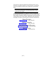
OPERATING AND MAINTENANCE
INSTRUCTION MANUAL
DAVID-III
MODEL 718
FM-STEREO PROCESSOR / GENERATOR
USER S RECORD
Model 718
--
Serial No. ____________
Date Purchased __________________
Warranty Card Mailed?
o
OPERATING AND MAINTENANCE
INSTRUCTION MANUAL
DAVID-III
-
MODEL 718
FM-STEREO PROCESSOR / GENERATOR
June, 2004
1305 Fair Avenue Santa Cruz, CA 95060
TEL: (831) 458-0552
FAX: (831) 458-0554
Visit our Website: www.inovon.com
TABLE OF CONTENTS
Section I - INTRODUCTION
MODEL 718 PRODUCT DESCRIPTION ................................................................... 3
History
Features
MODEL 718 TECHNICAL SPECIFICATIONS ........................................................... 4
BLOCK DIAGRAM .................................................................................................... 5
Section II - INSTALLATION
UNPACKING AND INSPECTION .............................................................................. 6
MOUNTING .............................................................................................................. 6
Rack Requirement
Heat Dissipation
AC (MAINS) POWER ................................................................................................ 7
Fuseholder
Mains Voltage Selector
Power Cord
RADIO FREQUENCY INTERFERENCE (R F I) ......................................................... 7
Location
Ground Loops
LINE INPUT AND RANGE SELECTION .................................................................... 8
Input Connections Unbalanced Inputs
Input Grain Range Gain Jumpers
PRE-EMPHASIS SELECTION................................................................................... 9
COMPOSITE/MPX OUTPUT ..................................................................................... 9
Section III - SETUP AND OPERATION
PANEL CONTROLS AND INDICATORS ................................................................. 10
NORMAL SETUP PROCEDURE ............................................................................. 12
INPUT GAIN Calibration
MPX LEVEL Adjustment
TRIBAND PROCESSING SETUP GUIDELINES ...................................................... 14
AGC Section Notes
MASTER DRIVE
BASS and BRILLIANCE
FINAL PEAK CONTROL ........................................................................................ 16
PIPP* LIMITER
COMP. CLIPPING
HOW DOES IT SOUND? ....................................................................................... 17
Section IV - CIRCUIT DESCRIPTIONS
INTRODUCTION..................................................................................................... 18
Component Annotation
A PWM PRIMER ..................................................................................................... 18
PWM Gain Control Feedforward Processing
Soft Knee
The PWM Ramp Waveform
1
PWM RAMP CIRCUITS ...........................................................................................20
Master Clock
Compressor/Limiter Ramp
AGC Ramp
SIGNAL PATH CIRCUITRY .....................................................................................21
INPUT STAGES ......................................................................................................21
Line Input Balancing INPUT LEVEL Control AGC Stages
AGC Gating AGC Metering Pre-Emphasis Program Pre-Clipping
TRIBAND PROCESSING ........................................................................................23
Band Division Band Rectifiers Midband Time Constants
Bass Processing Brilliance Processing PWM Comparators
Gain Reduction Indicators Combining Amplifier
THE PIPP* LIMITER ...............................................................................................27
LOW-PASS FILTER ................................................................................................28
Filter Overshoots Overshoot Compensation
The Low-Pass Filter
PILOT AND SUBCARRIER SYNTHESIS .................................................................29
Clock
Pilot Generation Center Sampling Subcarrier Generation
Composite Clipper Combining Amplifier Output Filter
Output Phase and Equalization Trimmers
POWER SUPPLY.....................................................................................................31
YOUR NOTES AND DOODLES...............................................................................31
Section V - APPENDIX
EXPLANATION OF PARTS LISTINGS ....................................................................34
PARTS LISTINGS ...................................................................................................34
PARTS SUPPLIERS.................................................................................................36
SCHEMATIC DIAGRAMS .......................................................................................38
INOVONICS WARRANTY ........................................................ (INSIDE BACK COVER)
2
Section I
INTRODUCTION
MODEL 718 PRODUCT DESCRIPTION
History
Inovonics introduced the first DAVID (as in David vs. Goliath) FMStereo Processor / Stereo Generator in 1992. The original Model
715 was the hallmark of simplicity, having been developed to
address the more basic of FM radio broadcasting needs.
The next generation DAVID-II came out in 1995. It included a
redesigned pulse-width-modulation audio processing section, which
helped to expand the applicability of this updated product to
broadcast situations where perceived loudness and modulation
density were considered germane to the broadcaster s success.
This third-generation DAVID-III brings even more features and
functionality to the modestly priced DAVID series, along with a
bigger, bolder and brighter sound. Wider AGC capture, multiband
processing, equalization adjustments and a proprietary final limiting
system make the DAVID-III the rival of far more expensive
alternatives.
Features
Leading features of the DAVID-III include:
•
Comprehensive PWM audio processing with gainriding AGC, three bands of compression and
limiting, and adjustable bass and brilliance EQ.
•
Inovonics unique PIPP* final limiter, which
assures full carrier modulation with all types of
program material.
•
A stereo-generator section that utilizes digitalsynthesis techniques for best stereo separation and
rock-stable operation.
•
A built-in, user-adjustable composite clipper.
•
A product that is simple to install and very easy to
use, the DAVID-III is built with easy-to-find
generic components for easy servicing anywhere
in the world.
3
MODEL 718 TECHNICAL SPECIFICATIONS
Processing Control:
Master processing drive is adjustable between 0dB and more than
12dB, equating to a corresponding
reduction in program dynamics and
apparent loudness increase.
Frequency Response (through an
appropriate de-emphasis network):
±0.5dB, 20Hz-15kHz; 60dB or
better at 19kHz.
Noise:
Better than 70dB below 100%
modulation in demodulated L/R
audio, 20Hz-16kHz. Individual
digital noise components above
54kHz are 70dB or better.
Equalization:
Adjustment range relative to
original program balance:
BASS: 3dB to +9dB
BRILLIANCE: 3dB to +6dB
(See Figure 4, Page 15.)
Distortion:
<0.5% THD in baseband and
subcarrier at 95% modulation with
PIPP* limiter defeated; <1.5% at
any level of modulation with PIPP*
limiter engaged.
PIPP* Final L/R Limiter:
Patented Polarity-Independent
Peak Processing circuitry assures
full modulation of the FM carrier
despite abnormalities in the
program waveform geometry.
Stereo Separation (LàR or RàL):
>55dB, 20Hz-16kHz.
Digital Synthesis Sampling Rate:
608kHz (16X subcarrier
oversampling).
Crosstalk (MàS or SàM):
Nonlinear crosstalk is better than
50dB, 50Hz-15kHz. Linear
crosstalk (through processing and
filters) is better than 40dB.
Composite Processor:
Adjustable from 0dB to 3dB clipping
of the 100%-modulated multiplex
waveform prior to pilot injection.
L/R Program Line Inputs:
Active-balanced/bridging XLR
inputs accept nominal program line
levels between 15dBu and
+10dBu.
Stereo Pilot:
19kHz, ±1Hz; injection level
adjustable between 6% and 12%,
relative to 100% modulation.
AGC Amplifier:
Unobtrusive, average-weighted
correction for long-term input level
variations; ±15dB capture range.
Composite (Multiplex) Output:
Adjustable between 1V p-p and
8V p-p; 75-ohm source impedance.
Pre-emphasis:
75µs or 50µs selected by circuit
board jumpers.
Power Requirements:
105 130VAC or 210 255VAC,
50/60Hz; 15 watts.
3-Band Processing:
Tight peak control in three asymmetrical frequency bands with
secondary platform time constants
to compress program dynamics with
average-value weighting. Crossover
frequencies at 100Hz and 4kHz.
(See Figure 7, Page 24.)
Size and Weight:
1¾ H x 19 W x 8 D (1U);
8 lbs (shipping).
4
BLOCK DIAGRAM
Figure 1, below, is a simplified Block Diagram of the DAVID-III. A
full set of schematic diagrams appears in the Appendix, Section V.
Figure 1 - Block Diagram, DAVID-III
5
Model 718
Section II
INSTALLATION
UNPACKING AND INSPECTION
As soon as the equipment is received, inspect carefully for any
shipping damage. If damage is suspected, notify the carrier at once,
and then contact Inovonics.
We recommend that you retain the original shipping carton and
packing materials, just in case return or reshipment becomes
necessary. In the event of return for Warranty repair, shipping
damage sustained as a result of improper packing for return may
invalidate the Warranty!
IT IS VERY IMPORTANT that the Warranty Registration Card found at the front of this Manual be completed
and returned. Not only does this assure coverage of the
equipment under terms of the Warranty and provide a
means of tracing lost or stolen gear, but also the user will
automatically receive specific SERVICE OR MODIFICATION INSTRUCTIONS should the factory issue them.
MOUNTING
Rack
Requirement
Heat Dissipation
The DAVID-III mounts in a standard 19-inch equipment rack and
requires only 1¾ inches (1U) of vertical rack space. The use of
plastic washers is recommended to protect the painted finish around
the mounting holes.
Consuming about the same power as a couple of night-lights, the
718 itself generates negligible heat. The unit is specified for
operation within an ambient temperature range extending from
freezing to 120°F/50°C. But because adjacent, less efficient
equipment may radiate substantial second-hand heat, be sure that
the equipment rack is adequately ventilated to keep its internal
temperature below the specified maximum ambient.
6
AC (MAINS) POWER
Fuseholder
The fuseholder is at the far left of the front panel. Apply downward
pressure and pull the cap outward to access the 5mm mains fuse.
Note that the cap has space for a spare fuse as well, though a spare
has not been included due to our ongoing diligence in keeping costs
low. The cap is reseated by reversing the removal process. This
fuse also serves as a front-panel emergency power disconnect for the
DAVID-III.
Mains Voltage
Selector
Unless specifically ordered for export shipment, the DAVID-III is set
at the factory for operation from 115V, 50/60Hz AC mains. This can
be confirmed by checking the designation beneath the mains
connector on the rear panel. The inappropriate voltage and fuse
value will have been crossed out at the factory with an indelible felt
marker.
To change the mains voltage, first remove the top cover of the unit.
A clearly marked slide switch is next to the AC mains connector on
the circuit board. With power disconnected, use a small screwdriver
to set the switch for 115VAC or 230VAC operation.
Be sure to install the appropriate fuse listed on the rear panel. You
can remove the factory strikethrough with a carcinogenic solvent
and then cross out the inappropriate marking with an indelible felt
pen.
Power Cord
The detachable IEC-type power cord supplied with the encoder is
fitted with a North-American-standard male plug. The individual
cord conductors may be color-coded in either of two ways:
1) In accordance with US standards:
BLACK = AC HOT
WHITE = AC NEUTRAL
GREEN = EARTH GROUND
2) To European CEE standards:
BROWN = AC HOT
BLUE = AC NEUTRAL
GRN/YEL = EARTH GROUND
RADIO FREQUENCY INTERFERENCE ( R F I )
Location
Ground Loops
Although it is natural for the DAVID-III to be installed alongside
high-power transmitters, please practice reasonable care and
common sense in locating the unit away from abnormally high RF
fields.
Because the unbalanced COMPOSITE/MPX OUT connector of the
DAVID-III is referenced to chassis ground, a mains frequency or RF
ground loop could be formed between output cable shield ground
and the AC power cord ground. A ground-lifting AC adapter may
well remedy such a situation, though the chassis somehow must be
returned to earth ground for safety. Generally, being screwed-down
in the equipment rack will satisfy the safety requirement.
7
LINE INPUT AND RANGE SELECTION
Input
Connections
The DAVID-III has electronically-balanced (transformerless) leftand right-channel PROGRAM LINE INPUTS. These appear as XLR
female connectors on the rear panel. As these are bridging, high
impedance inputs, they provide no termination for the console or
other equipment that feeds the DAVID-III. Most professional
equipment nowadays has low output impedances and high input
impedances. The concept of 600-ohm line matching dates from
the age of transformer coupling and is rooted in ancient telephone
practices. With few exceptions, audio line impedance matching is
ridiculed by today s hip broadcasters (you) and equipment
manufacturers (us).
Unbalanced
Inputs
The DAVID-III may be fed from gear with unbalanced outputs.
Disco mixers have proven perfectly serviceable for an installation on
a tight budget. For unbalanced lines, the single center conductor of
the shielded input lead should be connected to Pin 2 of the XLR
connector, and the shield connected both to Pin 1 and to Pin 3.
Input Gain
Range
The DAVID-III can accommodate line-level program inputs with a
nominal Zero-VU level between 15dBu and +10dBu. This 25dB
range is divided into two more manageable, overlapping gain ranges
that are selected by a series of four internal jumpers.
As shipped, the DAVID-III is set up for professional level inputs that
lie in the 0dBu to +10dBu range. Most console and STL receiver
outputs will fall into this range; +4dBu and +8dBu are typical
program line levels.
Lower levels, between 15dBu and 0dBu, may be encountered when
interfacing with semi-pro gear or with feeds from lossy studiotransmitter telephone line circuits. Extra gain for the low level
range is enabled by changing jumpers beneath the top cover.
Gain Jumpers
Under the top cover and just behind the left channel input connector
you will find four, 3-pin jumper strips. These are identified as JP2
through JP5 in the circuit board legend, and each has a push-on
jumper shunt. LO and HI designations identify the jumper
position for low-level and high-level inputs, respectively, and all four
jumpers must be set identically. This is shown in Figure 2, below.
Jumpers for HIGH LEVEL Inputs
Jumpers for LOW LEVEL Inputs
Figure 2 - Input Gain Range Jumpering
8
PRE-EMPHASIS SELECTION
The DAVID-III supports both the 75-microsecond FM broadcasting
pre-emphasis standard common to the Western Hemisphere and
parts of the Orient, and the 50-microsecond standard used in Europe
and Asia. Pre-emphasis appropriate to the delivery destination is
set at the factory, but this can be changed if necessary.
Beneath the top cover, locate the two, three-pin jumper strips
labeled JP1 and JP6. These are located in the rows of components
behind the left channel XLR connector and just either side of IC49.
The push-on jumper shunts may be moved between the 50 and 75
positions, and both jumpers must be set identically as shown in
Figure 3, below.
Jumpers for 75µs
Jumpers for 50µs
Figure 3 - Pre-Emphasis Jumpering
COMPOSITE/MPX OUTPUT
The unbalanced COMPOSITE/MPX OUT BNC connector on the rear
panel of the DAVID-III has a resistive source impedance of 75 ohms.
This allows cable runs of moderate length (to about 50 feet) to the
exciter or microwave link input. If the cable is more than just a few
feet, the cable itself should have a 75-ohm characteristic impedance
and be terminated in 75 ohms at the far end.
A Stereo Generator must always be connected to an exciter or link
(STL) input specifically intended for multiplex stereo. This is a
wideband, flat input, not a monaural program line input with its
own pre-emphasis network. Program signal pre-emphasis is
imparted by the DAVID-III.
9
Section III
SETUP AND OPERATION
PANEL CONTROLS AND INDICATORS
A brief description of the front-panel controls and indicators follows.
Explanations are arranged right-to-left, which is the order of the
signal path through the DAVID-III. Please at least skim over this
section to verify that our terminology agrees with your
understanding. More detailed notes on DAVID-III operation follow
this initial descriptive information.
The screwdriver-adjusted, front-panel multiturn trim controls
require fifteen to twenty complete rotations of the adjusting screw to
cover their total operating range. Depending on the manufacturer,
the end of the range may, or may not, be identified by a click-click
sound or other audible/tactile sensation.
INPUT
GAIN
A single control adjusts input sensitivity for both the left
and the right program channel inputs. The single
control makes DAVID-III setup easier, but provides no
means of correcting for channel imbalance. Stereo
imbalance should be addressed at the source of this
problem.
The INPUT GAIN control has a 12dB range, which is
extended by the input gain range jumpering options
described on Page 8. INPUT GAIN is adjusted using
normal program material to maintain the indicated AGC
gain in the center of its operating region.
GATE
OPEN
DAVID-III AGC is gated, meaning that during brief
pauses in the program the gain is locked to prevent
background sounds from slowly increasing to unnatural
proportions. The green GATE OPEN indicator will
remain continuously lighted during most music
programming, but will blink off during pauses in speech.
A.G.C.
GAIN
This series of seven LEDs displays the amount of
correction in effect for long-term variations in the
program level. The AGC circuit is average-responding
and is left/right correlated; that is, the overall circuit
gain is controlled by the greater of the left or the right
channel signals. This measure is incorporated to
preserve the program s stereo image.
AGC correction rate is intentionally quite slow. With a
conscientious operator at the console, the indicated A.G.C.
GAIN should always hover near the 0dB indicator.
10
The safe operating zone of the AGC circuit is within the
central three green LEDs. Consistent operation at +10dB
or 10dB suggests that the INPUT GAIN control should be
readjusted. If either the +15dB or the 15dB indicator
becomes lighted to full brightness, the input program
signal is definitely out of limits and the reason should be
found and corrected at once.
MASTER DRIVE
G/R
This is the first adjustment for audio signature in the
processing chain. It represents the input level control to
the Triband Processing section of the DAVID-III. As
well as adjusting the program level, this control also
affects dynamic compression release characteristics,
which become more aggressive as the control is rotated
clockwise. Additional details are presented under
TRIBAND PROCESSING SETUP GUIDELINES on Page
14.
The three sets of G/R (Gain Reduction) LEDs provide a
visual display of the approximate amount of peak-plusaverage gain reduction in effect in each of the three
processing bands, as well as giving an indication of the
compression release characteristic.
The green 0dB indicator remains lighted at full brilliance
with full gain (no processing) in the attendant band.
When the 12dB LED is lighted fully, 12dB or more
limiting and compression is in effect. Equal brightness in
both LEDs would suggest about 6dB of gain reduction.
With a little practice it should not be difficult to visually
interpolate for intermediate G/R values, as well as to
differentiate the fast limiter release from the slower
compression platform timing characteristic.
BASS
and
BRILLIANCE
PIPP* LIMITER
Because the effect of these two controls is largely
dependent on dynamics of the program source, they
cannot be thought of as simple EQ (equalization)
adjustments. What these afford is leverage over the
relative amount of total energy at the frequency
extremes of the program audio spectrum. Refer to the
more detailed discussion under the TRIBAND PROCESSING SETUP GUIDELINES on Page 14.
PIPP* is an acronym for Polarity-Independent Peak
Processing. In a nutshell, positive and negative program
peaks are limited independently of one another. This
ensures full modulation of the FM carrier and an audible
increase in program perceived loudness. Refer to the
more detailed discussion under the FINAL PEAK
CONTROL subhead on Page 16.
11
COMP. CLIPPING
MODE
In the fully counterclockwise OUT position of this
control, an output safety clipper catches only those
occasional, very fast peaks or overshoots that sneak by
the earlier protection circuitry in the signal path. As
COMP. CLIPPING is rotated clockwise, the level applied
to this safety clipper is increased by the dB value shown
by the panel markings.
MODE simply switches the operation of the DAVID-III
between normal multiplex stereo transmission and
forced-monaural operation. In the MONO mode, both
the 19kHz stereo pilot and the 38kHz subcarrier are
turned off, and left and right program channels are
summed.
FUSE / DISCONNECT
The front-panel fuseholder also provides a means of
disconnecting AC mains power in an emergency. Push
the fuseholder cap down and pull it away from the panel
to interrupt power.
NORMAL SETUP PROCEDURE
This setup procedure presupposes a normal installation with the
DAVID-III PROGRAM LINE INPUT fed directly from the output of
the audio console, and with a direct connection from the
COMPOSITE/MPX OUTPUT to the wideband input of a transmitter
exciter. Variations from these conditions, such as an intermediate
STL (or other link) in either the input or the output path of the
DAVID-III may call for considerations not addressed here.
At this point the DAVID-III should be installed in the program chain
with power applied. The MODE switch should be in STEREO and
the PIPP* LIMITER switched ON.
INPUT GAIN
Calibration
The single INPUT GAIN adjustment controls both stereo channels
simultaneously. It is set simply to center the AGC operating range
with a nominal Zero-VU program line input of typical program
material. If this procedure shows control range to be outside
adjustment limits, recheck circuit board jumpering for Line Input
Range Selection as described on Page 8.
With program from the console or link receiver feeding the DAVIDIII, adjust the front-panel INPUT GAIN control so that the A.G.C.
RANGE indicator hovers around the 0dB mark most of the time.
If this procedure is performed properly, and if the operator pays
reasonable attention to console metering, the AGC GAIN indicators
should normally hover around 0dB, and always remain in the safe
operating zone between 10dB and +10dB.
MPX LEVEL
Adjustments
This part of the procedure is performed on-air under normal
operating conditions and using typical program material. You must
have access to the station s Modulation Monitor. An RDS or SCA
subcarrier should not be connected until Step 6.
12
PLEASE be certain that you understand operation of the ModMonitor, and that it is properly calibrated and connected to the
correct transmitter RF sample point or has a solid off-air signal.
1. Put the Mod-Monitor in its Total Peak Modulation
measurement mode with peak flasher(s) set to 100%.
2. Just for this calibration procedure, turn the MASTER DRIVE and
COMP. CLIPPING controls fully clockwise (maximum).
3. With normal program fed to the DAVID-III (at a level that
maintains A.G.C. GAIN in the center of its range), adjust the
MPX LEVEL control for a Mod-Monitor indication of frequent
100%-modulation peaks.
4. Back-down the MPX LEVEL control slightly, so that the 100%
peak flasher(s) light only occasionally.
5. Switch the Modulation Monitor to display the injection level of
the 19kHz stereo pilot.
6. Adjust the PILOT INJ. control for a 9% Mod-Monitor reading of
pilot injection.
7. OPTIONAL: If an RDS or an SCA subcarrier is to be
transmitted, connect it to the proper combining point at this
time. Using the Mod-Monitor or other means of reading the
auxiliary subcarrier injection level, adjust the subcarrier level
control for the proper injection. This is normally about 4% for
an RDS subcarrier and 10% for an audio SCA.
8. Put the Mod-Monitor back into its Total Peak Modulation
measurement mode and, if necessary, trim the MPX LEVEL
control so that the peak flasher(s) indicate only occasional 100%
peaks.
9. NOTE: Depending on current operating rules and practices,
total peak carrier deviation may be permitted to exceed the
customary 100%-modulation figure when SCA and RDS
subcarriers are broadcast,. The station (or consulting) engineer
should be aware of legal guidelines in effect and assume
responsibility for any adjustment that results in a total
modulation reading in excess of 100%.
10. Decrease the COMP. CLIPPING and MASTER DRIVE controls to
their normal operating values. As a starting point, set COMP.
CLIPPING to 1dB and MASTER DRIVE to +6dB.
13
TRIBAND PROCESSING SETUP GUIDELINES
Processor setup is obviously very subjective and will depend entirely
on the station s format, the desired sonic signature, and the needs,
wants and whims of various station personnel. A few hints are
provided here, some of which are redundant to information that has
already been given with the identification of the various front-panel
appointments.
AGC Section
Notes
The slow, gain-riding AGC action of the DAVID-III departs from
earlier versions in this series of processors. The response to
program material is average-responding rather than peakresponding. The rationale behind our about-face on this issue has to
do with the tendency toward greater and greater processing of music
source material. Although the popular CD is only a consumer music
format, it is nonetheless capable of a full 90dB dynamic range.
Sadly, a statistical analysis of most CDs on the market will show
total dynamics of 20dB or less, except for fade-ins and -outs.
An averaging response to program dynamics encourages the
downstream Triband Processing section of the DAVID-III to work
harder on source material with a greater dynamic range as indeed
it should. Under our previous position, pre-squashed music would
get just as much compression and peak processing as wide-dynamics
live announce certainly more than it needs. This would constitute
a case of overprocessing of the musical content of the program.
The correction rate of the AGC stage has been speeded-up from
previous DAVID versions by a factor of four. The present value is
about 2dB/second, just a bit slower than would result in audible
dynamic alteration of the program, given the averaging response to
music and speech.
MASTER DRIVE
This sets the amount of overall processing. When set at 0dB, there
is little-if-any dynamic gain reduction ever in effect, except with
program material having a high average-to-peak ratio; an
unprocessed announce-microphone channel, for instance.
Normal MASTER DRIVE range extends from 0dB to +12dB. These
figures reflect the approximate amount of program dynamics
compression called into play, and to a subjective extent the amount
of increase in loudness. Loudness increase will depend largely on
the dynamic range of the unprocessed program material. Obviously
if the source CD is already highly compressed there s not much that
can be done to further decrease the average-to-peak ratio.
The designation MAX will be noted at full clockwise rotation of the
MASTER DRIVE control. Between +12dB and MAX, Triband
Processing release timing is jumped-up to its fastest rate. This nth
degree adjustment can yield a loudness increase, but at the expense
of audible artifacts with some program material, notably solo voice.
Please use discretion with this maximum setting.
A good starting point for MASTER DRIVE is +6dB. Listening tests
with a variety of program material may suggest an alternative
14
setting. Also, adjustment of BASS and BRILLIANCE may dictate a
change in the MASTER DRIVE setting.
BASS and
BRILLIANCE
Circuit action of BASS and BRILLIANCE is threefold. First, the
setting dictates to what extent midband gain reduction
simultaneously controls the amount of reduction at the frequency
extremes; that is, the amount of coupling between the bands.
Secondly, as BASS and BRILLIANCE are rotated clockwise, not only
do these bands decouple from the midband section, but they also are
allowed to release beyond the final midband release point. Thirdly,
clockwise rotation of these controls speeds up the release timing in
the subject band. These three functions work together to create
what we call Spectral Loading, best defined as an artificial buildup
of energy at either or both of the frequency extremes. This is quite
different from static (fixed) equalization.
When BASS and BRILLIANCE are set to 0dB, the Triband Processing
section works almost like a single-band compressor. Tonal balance
will be much the same as the unprocessed program input, though
the program dynamic range will be restricted based on how MASTER
DRIVE has been set. Rotating BASS and BRILLIANCE toward -3dB
will cause a reduction of energy at the ends of the spectrum.
The BASS control gives up to 9dB of low-end Spectral Loading.
BRILLIANCE, however, affords only a maximum 6dB. BRILLIANCE is
purposely restricted because of FM broadcast system pre-emphasis.
With high frequencies already accentuated by 10dB or more,
attempts to create additional top-end sparkle or crispness in the
program runs the risk of causing a sound that is either brittle
(clipped) or mushy (excessively HF-limited). Exercise discretion
with extremes in Spectral Loading, particularly at the top end.
Figure 4, below, illustrates the frequency range and leverage of the
BASS and BRILLIANCE controls. Keep in mind that Spectral
Loading is a dynamic function, and that maximum effect will depend
largely on the tonal balance of the program material.
Figure 4 - Spectral Loading Range and Leverage
Note in Figure 4 that the BASS control shows a second-order
Chebychev filter characteristic with the expected dip prior to boost
and a peak prior to cut. This is a product of the band-splitting
15
architecture that actually gives an advantage in the DAVID-III.
Note that the dip falls in the lower voice range. Thus when bass is
boosted voices won t tend to become tubby.
FINAL PEAK CONTROL
PIPP* LIMITER
As previously defined, PIPP* is an acronym for PolarityIndependent Peak Processing. This function separates the gain
control action between the positive and negative excursions of the
program waveform, with the zero-volt DC baseline of the incoming
signal as the point of reference.
This elementary explanation will undoubtedly elicit a horrified
response of, But that adds distortion! Well, yes and no. The only
truly undistorted waveform that we can measure, or perceive as a
pure tone by ear, is a textbook sinewave. Because a sinewave is
perfectly symmetrical, the PIPP* limiter acts equally on both the
positive and the negative excursions and thus does not distort the
wave shape in the slightest.
An asymmetrical waveform, on the other hand, most notably a solo
musical instrument or speech, will have asymmetry and peakiness
removed by the PIPP* limiter. Does this imply that the waveform,
by definition already full of harmonics (ie: distortion!) will further
be distorted ? Technically, yes. A saxophone may sound more
saxophone-like and speech will definitely have a different quality.
But, after all, we are talking audio processing here, and sonic
modification is par for the course.
Another possible concern might be that mucking-about with
waveform symmetry could introduce a sufficient DC component to
the program that the exciter frequency-reference PLL would unlock.
Take comfort in the fact that audio program material is constantly
changing, and DC offsets are short-lived. Not to worry.
The primary advantage of the PIPP* concept is full negative and
positive deviation of the carrier with all types of program material.
This adds up to a louder sound with a special added bonus of
beefier bass. Now, if the PIPP* concept worries or offends you, or
if you think it doesn t sound quite right, we have provided a little
switch to disable the feature quickly and easily.
The two LEDs associated with the PIPP* limiter show circuit action
in the separate and independent left and right channel limiters. The
resting state of the LEDs is yellow. When positive excursions are
being limited the LED goes red; when negative excursions are
limited the LED turns green.
It is interesting to watch the constant color change of the two PIPP*
LEDs as the program is worked-on, and especially to observe the
symmetry difference between stereo channels. By operating on each
channel independently, the PIPP* limiter actually introduces a
16
small additional amount of stereo difference information. This gives
a little bit of stereo enhancement at no extra charge.
Further discussion of the PIPP* limiting concept can be found in a
white paper on the Inovonics Website: www.inovon.com. PIPP*
limiting is protected by US Patent No. 6,658,120.
COMP.
CLIPPING
Composite clipping has traditionally been the tool used to squeeze
the very last bit of loudness from the processed FM program signal.
Too much clipping of the multiplex signal can generate spurious
harmonic products that clutter the baseband spectrum, interfering
with the 19kHz pilot and compromising performance of RDS and
SCA subcarriers.
In the DAVID-III the multiplex waveform is clipped prior to the
point at which the 19kHz stereo pilot is inserted. This ensures that
the pilot is not directly modulated, though the pilot is not protected
from harmonic products that are generated as the program
waveform is clipped at fractional intervals (mostly one-third and
one-fifth) of the pilot frequency. The following tabulation is an
approximation of the SGTM (Spectral Garbage) generated by
composite clipping:
COMPOSITE
PROCESSING
PEAK VALUE OF
CLIPPING PRODUCTS
OUT
1dB
2dB
3dB
>60dB below 100% Mod.
50dB below 100% Mod.
45dB below 100% Mod.
40dB below 100% Mod.
Keep clearly in mind that crosstalk of program audio harmonic
components into the RDS or SCA subcarrier region is exacerbated
by composite clipping, so use this feature sparingly! Generally, 1dB
of COMP. CLIPPING can be tolerated without harmful effect.
HOW DOES IT SOUND?
The foregoing overview of processor setup is intended only as a
guide. Final decisions must be made based on extensive listening
and not on the basis of numbers. The dB markings around the
front-panel controls correlate well with what s going on inside the
DAVID-III, but not necessarily with what you may expect to hear.
Please make every effort to arrive at a setup that sounds good to you
and to other station personnel for the majority of program content
and over the long term. Resist the temptation to change settings
because of how one or two specific music tracks sound; some songs
simply sound awful with any processing or without it, for that
matter.
17
Section IV
CIRCUIT DESCRIPTIONS
INTRODUCTION
This Section details the circuitry of the Inovonics DAVID-III.
Circuit descriptions refer to the six sheets of Schematic Diagrams
contained in the Appendix, Section V, Pages 38 to 43.
Component
Annotation
DAVID-III schematics may appear to have component reference
designations assigned in a haphazard manner. Rather than to
annotate the schematic in a logical sequence, we have instead chosen
to designate the components on the circuit board in a logical top-tobottom and left-to-right manner, following the physical placement of
the parts in their neat little rows. It is our expectation that this
practice will make any necessary troubleshooting easier, as a
component can physically be located quickly following analysis of
the schematic.
A PWM PRIMER
PWM Gain
Control
The DAVID-III utilizes Pulse-Width Modulation techniques rather
than VCAs (voltage-controlled amplifiers). This technology, as
applied to broadcast audio processing, was pioneered by Inovonics in
the early 1980s and has been refined over the years. PWM is a
simple, colorless, quasi-digital method of linear gain control that
avoids several hassles associated with more expensive and possibly
single-sourced VCA integrated circuits. Our implementation of
PWM utilizes the popular 4000-series CMOS parts that are dirt
cheap and available in any civilized area.
PWM sets the gain of an analog circuit simply by sampling, or
chopping, the analog signal; that is, turning it on and off at a rapid
rate. Consider an audio program signal which can be turned on and
off with a toggle switch. When the switch is on, attenuation is zero.
When off, attenuation is infinite. If we satisfy Dr. Nyquist s axiom
and toggle this switch at a rate at least twice that of the highest
audio frequency, linear signal attenuation becomes directly
proportional to the OFF time as depicted in the chart at the top of
the next page.
The DAVID-III sampling rate is 152kHz, about ten times the highest
program audio frequency. Since this is well above the Nyquist rate,
anti-aliasing and reconstruction filters can be simple and gentle.
18
PWM GAIN CONTROL ACTION
Switch ON
Switch OFF
Attenuation
100%
0%
0dB
50%
50%
6dB
25%
75%
12dB
10%
90%
20dB
1%
99%
40dB
Feedforward
Processing
The Triband Processing section of the DAVID-III operates in a
feedforward mode, rather than using the more traditional feedback
method. The amplitude of the input signal establishes circuit gain
to hold the output constant at a 100%-modulation ceiling value.
Feedforward limiting necessitates a conversion factor to give one dB
of output attenuation for each dB that the input signal increases.
Put into linear (voltage), rather than log (dB) terms, this function is
expressed as x=1/y. Figure 5 graphs this function. x represents the
circuit gain needed to hold the output at a constant 1-volt value,
with an input, y, that increases from 1 volt to 10 volts. This
technique becomes a bit precarious at small duty cycles (attenuations of 40dB or more), but in the 0 to 30dB range typically required
for audio processing, PWM is easily implemented, perfectly
predictable, and without sonic coloration.
Figure 5
Voltage Transfer
Function
Assuming a linear relationship between PWM on/off time and signal
gain reduction, the 1/y expression translates directly to the duty
cycle; that is, 0.1 is a 10% ON time, and 1.0 a 100% ON time.
Soft Knee
In the example above, 1 volt represents a threshold level, below
which gain will remain at full value. In practice, the threshold is
adjusted to conform to what has become known as a soft knee
characteristic. This means that the program signal eases gently into
compression and limiting to avoid the abrupt change from a linear
19
compression and limiting to avoid the abrupt change from a linear
to a limited state that characterizes traditional feedback topology.
The soft knee is normal behavior for feedforward gain control, and
is credited for the smoother, less fatiguing sound attributed to this
method.
The PWM
Ramp
Waveform
Figure 6 shows the waveform that is generated by the DAVID-III to
affect the desired feedforward transfer characteristic. Note the
similarity between this waveform and Figure 5, but with the
addition of an extended droop to the right. This droop gives the
soft knee compression/limiting threshold. A negative-going
pedestal has also been added to keep the CMOS analog switches
active, even when no gain reduction is in effect.
Figure 6
DAVID-III PWM
Ramp Waveform
V=2V/div.
H=1µs/div.
This ramp runs continuously at a 152kHz rate. It is applied to one
input of a comparator, and a DC voltage derived from the input
signal is fed to the other comparator input. The comparator output
is the duty-cycle-modulated squarewave that chops the program
audio signal.
PWM RAMP CIRCUITS
Master Clock
Referring to the Sheet 6 of the Schematic on Page 43, IC3D is the
DAVID-III master clock running at 1.216MHz, which is 64 times the
stereo pilot frequency. IC3C is a buffer, and binary dividers IC21A,
IC43A and IC43B derive the 152kHz PWM switching frequency.
This is the PROC CLOCK that is picked up on Sheet 3 of the
Schematic, Page 40.
Compressor/
Limiter Ramp
The 152kHz PROC CLOCK is buffered by IC44D. The squarewave
differentiated by C107 and R302 creates a 200 nanosecond pulse at
the output of IC44C. The positive-going edge of the pulse turns on
Q25, which brute-forces the pedestal portion of the PWM ramp
waveform.
20
The negative-going edge of the 200ns pulse is inverted by IC44A and
differentiated by C93 and R267. The output of IC44B is a 100ns
negative pulse that turns on Q24 to charge C95 instantaneously to
about +6 volts.
C95 has a complex discharge path calculated to create the precise
PWM reference ramp waveform. The initial fast discharge is
through R272 and diodes CR44, CR45 and CR46. After an initial
discharge period, CR46 is biased out of the equation and discharge
continues through R273. When the voltage level falls below the
turn-on point of CR44 and CR45, the remaining discharge path is
through R271. The action just described produces the ramp
waveform of Figure 6, which is repetitive at the 152kHz rate. The
ramp is presented to one input of the three comparators that create
the PWM switching squarewave.
AGC Ramp
The 200ns negative-going pulse from IC44A, labeled AGC CLOCK,
may also be picked up on Sheet 1 of the Schematic, Page 38. This
pulse turns on Q26 to charge C109. This capacitor discharges
through R304 and R305 to create a separate, second ramp waveform
for the AGC stage. This discharge shape is a simple R/C function.
As the AGC stage works in a feedback mode, the R/C ramp gives a
constant dB-per-second control rate over the 30dB AGC range.
SIGNAL PATH CIRCUITRY
NOTE: Left and right program channel circuits are identical, so
only the left channel will be described in detail. A skilled technical
professional should be able to extrapolate the circuit descriptions for
the right channel.
INPUT STAGES
Line Input
Balancing
INPUT LEVEL
Control
Leafing to Page 38, IC48B is the program line input balancing
amplifier. JP2 and JP3 short-circuit resistors R358 and R359,
respectively, to give IC48B additional gain for low-level program
inputs.
A single multiturn potentiometer, R326, sets the DAVID-III input
sensitivity for both stereo channels. IC54B and IC55A include both
positive and negative feedback to create constant-current sources for
the left- and right-channel program signals feeding the two ends of
R326.
Despite appearances, INPUT GAIN control R326 does not operate as
an arm of a voltage divider. Constant-current feeds to the two ends
of this pot makes its attenuation of the program signal directly
proportional to the resistance to the grounded wiper. This means
that as the left channel signal decreases, the right channel level
increases, and vice-versa. But the backward-level-controlled right
channel program is combined out-of-phase with the raw right
21
channel input by IC54A, causing the right channel to track the left
channel output of IC54B. Many thanks to W. Stephen Woodward
and Electronic Design magazine s Ideas section for this clever one!
AGC Stages
The AGC amplifier is made up of two identical cascaded stages.
IC53B and IC51B are configured as second-order, low-pass filters
with gain. There is a CMOS analog switch at the input of each
stage, part of the 4-section IC52. The duty cycle, or on-versus-off
time, of this switch determines the gain of the circuit as tabulated at
the top of Page 19.
The AGC output is inverted by IC50B to afford full-wave
rectification by CR56 and CR57. The cathodes of these diodes are
common to those in the right channel to make AGC action
dependent on the greater of the two channels, thus preserving the
stereo image.
The rectified AGC output is integrated by R277 and C96, the output
of IC45B representing the average value of the program signal. This
derived DC voltage is identified as PGM AVG and is also employed
in the pre-emphasis stages.
IC45C compares the average program level with a DC reference
from the R310/R311 divider. When the program level exceeds the
reference, the output of IC45 goes high, charging C97 through R298
and R299. When the program level is below the reference, CR51 is
reverse-biased and C97 discharges through R299 and R297.
Integration by R299 and C97 determine the AGC correction rate.
DC buffered by IC45D is presented to one input of a comparator
comprised of Q27, Q28 and Q29. The AGC ramp is fed to the other
comparator input, and the output from Q29 is the PWM control for
the four IC52 analog switch sections.
AGC Gating
AGC in the DAVID-III is gated, meaning that gain does not slowly
increase out of proportion when no valid input signal is present.
R356 and R357 sum the left and right channels into IC46A. This
stage is also a first-order band-pass filter that favors voice
frequencies and desensitizes the gating circuit to air-conditioner
rumble and squeaky chairs. The L/R sum is full-wave rectified by
CR49, CR50 and IC46D. A short time constant of this rectifier is set
by R313, R314, C110 and C111.
When the input is low, below the gating threshold, the output of
IC46D goes positive. CR53 biases the DC reference for the AGC out
of the picture, and CR52 sets a fixed DC bias through R309, R298
and R297 that corresponds to the AGC 0dB resting point. Thus
when there s a pause in the program, AGC gain slowly returns to
zero. When the program is active, the output of IC46D goes
negative. This lights the GATE OPEN indicator, reverse-biases CR52
and CR53, and enables normal AGC action.
22
AGC Metering
Six op-amp sections monitor the output of IC45D and drive the
seven front-panel A.G.C. GAIN indicators. Each op-amp section has
gain and fixed-bias values to ensure that the seven A.G.C. GAIN
LEDs fade evenly over the 5dB indicated steps of gain.
Pre-Emphasis
Jumping down to Page 39, IC49B has integration in its feedback
path to effect proper program pre-emphasis. Jumper strip JP6
selects either the 75µs or the 50µs characteristic. Pre-emphasis
selection is described on Page 9.
Program
Pre-Clipping
The feedback path of IC49B also includes transistors Q32 and Q33.
These serve as hard clippers for program signal peaks, the clipping
point determined by DC bias applied to the transistor bases.
Program pre-clipping is keyed to the average value of the program
signal. This L+R program average value is derived from the output
of the AGC amplifier by IC45B. Time constants of R277 and C96
are relatively quick, so the PGM AVG voltage closely follows the
envelope of the L+R program signal.
The gain of IC45B maintains the PGM AVG DC voltage level at a
point 10dB to 12dB above the actual program audio level at the
output of IC49B. This means that when program dynamics exceed
an average-to-peak ratio typical of music and speech, program peaks
are hard-clipped.
The effect of clipping at this point is seldom ever audible. In the
first place, sadly few CD music tracks contain peaks more than 10dB
above the true-average level of the music. Secondly, clipping is in
the pre-emphasized domain. This means that clipping artifacts are
attenuated by receiver de-emphasis. Finally, the program-derived
DC value is a simple average and not based on an r.m.s. average of
the program signal. Repetitive peaks add to the average value
further to help bias the clippers out of the program.
For the most part, only transient, non-repetitive program peaks are
pre-clipped. Nonetheless, this action is quite effective in reducing
unnecessary Triband Processing action.
TRIBAND PROCESSING
Band Division
The DAVID-III works on the program audio signal in three
frequency bands. These are nominally BASS, MASTER (midband)
and BRILLIANCE. A graphic representation of band-splitting is
shown in Figure 7 on the next page.
Band division is obviously asymmetric. The three bands certainly
don t look as though they would recombine properly to give flat
overall response, but they do. Here s why.
IC35A is a second-order low-pass filter with rolloff beginning at
about 100Hz. The output of this stage is the bass band. This
output is subtracted from the program input by IC36A, which also
has a second-order low-pass function starting at about 4kHz. The
output of IC36A has the midband band-pass response shown in
23
Figure 7, including the 1dB hump at 175Hz. Note that the highpass characteristic of the midband is only first-order, even though it
was derived from a second-order subtraction. But wait, that s not
all!
Figure 7 - DAVID-III Triband Frequency Division
IC37A is yet a third subtraction stage. It subtracts both the
midband and the BASS band from the program input, and its output
is the brilliance band.
Now, as all three of the frequency bands were derived by subtraction
from the full-range program signal, there is no way that they can t
add back up to flat response and they certainly do. Moreover, not
only is the recombined amplitude response as flat as the proverbial
pancake, but the phase response is linear as well. Even as the gain
of a particular band is changed through Triband Processing action,
this circuit architecture is distinctly free of phase funnies and
amplitude peaks at the crossover frequencies.
Band Rectifiers
Midband Time
Constants
Each of the three band-splitting stages has a companion phase
inverter to provide full-wave rectification of each band output. DC
control voltages from each band are common to both the left and the
right channels to preserve stereo imaging. The DC control voltages
are identified in the schematic as BASS RECT, MSTR RECT and
BRILL RECT.
Flipping over to Page 40, C55 charges to the instantaneous peak
value of the midband program signal through R202. This peakderived DC is fed directly to the PWM comparator, Q17, Q16 and
Q15. The ramp waveform of Figure 6 is presented to the other
input of the comparator. The output of the comparator is a
squarewave, labeled MSTR PWM on the schematic. The duty cycle
of this squarewave is inversely proportional to the gain reduction
needed to maintain midband program level at a constant value.
This describes the feedforward gain control action.
C55 discharges through R162 into C54, and both capacitors
discharge through R164 to ground. The purpose of C54 is to provide
a release platform, which is defined as: 1) a secondary level to
which fast peak reduction can release quickly, and: 2) a level
representing the average value of gain reduction that can release
24
more slowly. This dual time constant separates the peak-limiting
and average-compression functions of DAVID-III processing.
C55 is never allowed to discharge completely to ground, however.
R174 and R175 provide a fixed bias, which is delivered to C55
through CR30. This bias maintains about 9dB of gain reduction in
the midband section at all times, an essential requirement of the
Spectral Loading feature.
The MASTER DRIVE control also factors into the equation. At full
counterclockwise (0dB) an additional amount of fixed DC bias is fed
to C55 through CR26 and R161; about another 12dB worth of gain
reduction, in fact. This serves to further reduce midband and, as we
shall see, overall gain through the system. This gain spoiling is
about equal to the average-to-peak ratio established by the preclipper ahead of the Triband Processing section. This means that at
the 0dB setting the average-responding AGC is largely responsible
for overall program signal leveling. Expected program peaks 10dB
to 12dB above the average program level will just drive transmitter
modulation to 100%. With the MASTER DRIVE pot at 0dB, there will
be very little if any processing of the incoming program aside from
gain-riding AGC.
As MASTER DRIVE is rotated clockwise, less and less of the gainspoiling voltage is applied to C55. As a result, program peaks
become more and more subject to processing in this section. When
MASTER DRIVE is at +12, only the quiescent 10dB worth of gain
spoiling from R174 is in effect, and processing is at maximum, so far
as levels are concerned.
As MASTER DRIVE is turned further clockwise, from +12 to MAX,
something else happens. The wiper of R183 begins to go negative
because of bias through R181. This has two effects. First, the
quiescent gain-spoiling voltage through R174 is reduced somewhat,
which has the effect of further increasing midband processing.
Secondly, the midband gain-reduction release platform developed by
the charge on C54 is eliminated because of negative bias through
CR27 and R163. This causes a fast release over the entire midband
gain-reduction range, which gives an apparent loudness increase
with some types of programming, but at the risk of some material
sounding choppy.
Midband gain-reduction voltage is integrated by R165 and C57. The
voltage across C57 represents the long-term average of gain
reduction in effect. This voltage is buffered by IC34A, which has
about a 3dB DC gain. This voltage, G/R+3dB, is connected to the
top of the BASS and BRILLIANCE adjustments.
Bass
Processing
C65 integrates the DC peak value of the rectified bass channel input
(BASS RECT), though integration is not instantaneous because of
series resistor R213. This resistor does not have the expected effect
of slowing down the bass limiter attack time, as the rectified input is
fed directly to the bass band PWM comparator, Q23, Q22 and Q21.
The charging of C65 is delayed, to be sure, which causes selfmodulation for the first few cycles of the bass waveform. This
imparts a delightfully gutsy quality to the attack of bass
25
imparts a delightfully gutsy quality to the attack of bass
instruments, making the bass sound phatter.
BASS control, R142, delivers variable amounts of gain-spoiling DC
bias to the gain-reduction circuitry. When set at 3, an amount of
DC equal to average midband gain reduction, plus an additional 3dB
due to gain in IC34A, becomes the reference for bass band gainreduction release. Bass peaks exceeding midband program energy
will be limited independently, but gain in the bass band will be
spoiled by the additional 3dB even at full release.
Set at 0dB, the wiper of R142 is at the same DC level as average
midband gain reduction. Bass peaks are independently limited as
required, but this section releases back only to the midband average
release level. At this setting the bass band is coupled, or slaved, to
midband gain reduction.
As BASS is turned progressively clockwise, the bass band is allowed
to release to a DC resting point that is actually lower than the
release point of the midband section. This brings Spectral Loading
into play, which increases the overall energy in the bass band. As
the midband has a full-release level that is spoiled by 9dB, program
bass can actually be enhanced by this same figure at full clockwise
rotation of the BASS control.
Primary bass band release is through R203, and is realized when the
BASS control is at +9. As gain-spoiling bias is introduced through
CR25, release slows down.
Brilliance
Processing
Because the brilliance band involves frequencies of 4kHz and up,
gain control action can afford to be very fast. Attack is near
instantaneous as C75 charges through R208. The integrated DC is
applied directly to PWM comparator Q20, Q19 and Q18.
Spectral Loading for the brilliance band is identical to that described
above for the bass band. The only difference is R214 inserted in the
clockwise leg of BRILLIANCE control R243. This limits the amount
of Spectral Loading to +6dB for the top end of the audio spectrum, a
figure in keeping with restraints imposed by FM transmission
system pre-emphasis.
PWM
Comparators
Gain Reduction
Indicators
Why in the world would anyone build a comparator from discrete
transistors instead of using an integrated circuit? For a couple of
reasons, actually. Most fast comparator ICs do not have sufficient
input dynamic range for DAVID-III applications; many have a
pathetic 5-volt restriction on the differential input range.
Comparators that have sufficient differential and common-mode
specifications aren t fast enough, and those that are speedy tend to
oscillate if you look at them wrong. Finally, three transistors cost a
fraction of what the one or two, single-sourced ICs cost that we
could have used in these spots.
G/R (gain-reduction) indicators utilize a simple differential amplifier
driving a pair of LEDs. In each of the three bands, the DC control
voltage is fed to one input of the differential amp and the compressor/limiter release level is fed to the other. Gain and offset of the
stages is such that the green LED glows at full brightness with no
26
stages is such that the green LED glows at full brightness with no
reduction in effect, fading to full-brightness of the red LED with
12dB of reduction. Midway through the display range, both LEDs
should be lit about halfway.
Combining
Amplifier
Back on Page 39, IC33B is a current-summing combining amplifier
and low-pass filter. The three frequency bands are summed through
resistors R235, R234 and R233, with a CMOS analog switch sections
in series with each.
Gain-control PWM drives the analog switches, the duty cycle
effectively multiplying the 3k series resistor. When the duty cycle is
50% in the bass band, R235 looks like 6k. At 10%, the effective
resistance is 30k. The current-summing configuration of IC33B
eliminates interaction between the bands, and the low-pass response
removes the 152kHz switching frequency.
THE PIPP* LIMITER
The operating theory of the PIPP* Limiter is detailed on Page 16.
Though the subject US Patent covers various analog and digital
implementations of the fundamental concept, the configuration used
in the DAVID-III is absurdly simple.
On Page 41, the program audio signal from the Triband Processor
section is routed to IC32B through R199 and R198. C68 and C69
turn this stage into a unity-gain low-pass filter.
The bases of Q11 and Q12 are connected to the junction of R199 and
R198. The emitters of these transistors are clamped at DC levels
representing the absolute output ceiling of the DAVID-III. Thus
Q11 and Q12 will always serve as hard clippers for program peaks
that exceed the assigned ceiling value. But each of these two
transistors is part of a voltage amplifier as well.
Using the Q12 side of the circuit for an illustration, as the program
signal approaches the final clipping point Q12 begins to conduct,
which turns on Q14 to begin charging C40. Voltage developed at the
top of C40 turns on Q5, which is connected to the program signal
path through R102 and CR18. As Q5 conducts, positive waveform
excursions are maintained at the clipping threshold, which becomes
the final-limiting point. This action describes a closed-loop,
feedback peak limiter for positive program peaks. CR18 ensures
that this part of the circuit has no effect over the negative-going
program components.
The emitter of Q5 is biased to a DC level that cancels the forward
drop of CR18 and the saturation voltage of Q5. A small amount of
program signal current is applied to the base of Q5 to linearize the
transistor s dynamic conduction resistance over the range of the
collector voltage swing.
27
Q11, Q13 and Q6 serve the same function for negative program
peaks. Control voltage for the positive and negative limiters is
summed by IC27D, which, with the help of its companion inverter,
drives a bi-color LED to indicate PIPP* Limiter action.
When the PIPP* Limiter is turned off by S3, R103 is switched into
the circuit. This attenuates the program signal by an amount equal
to the typical value of PIPP* Limiter gain reduction so that the
incoming program signal will not be clipped excessively by Q12 and
Q11 when the PIPP* circuit is not enabled.
LOW-PASS FILTER
Filter Overshoots
All low-pass filters exhibit a certain amount of overshoot and
ringing when presented with complex input waveforms. Generally,
the sharper the cutoff, the more pronounced the effect. Overshoots
result from the elimination of higher-order input signal components.
Prior to filtering, these components helped to define the signal peak
amplitude. Even a fully phase-corrected filter will exhibit
overshoots, and the 7-pole elliptic filter used in the DAVID-III can
overshoot 3dB or more!
Other systems of overshoot control permit the primary low-pass
filter to overshoot, then isolate and re-introduce the overshoots to
cancel themselves in the signal path. The patented overshoot
compensator in the DAVID-III, on the other hand, pre-conditions
the limited program signal ahead of the filter so that there is little
tendency for the filter to generate overshoots.
Overshoot
Compensation
Thumbing to Page 42, IC31B includes a phase-lag network that
displaces the fast leading and trailing edges of steep waveforms in
time. This means that the primary time-domain characteristic of a
program waveform that would normally excite filter overshoots is
instead added to the waveform amplitude. CR29 and CR28 are
biased to the limited/clipped level of the input program signal and
strip these displaced-and-added components from the phaselagged program waveform. IC29B is a differential stage that
compares the input and output of the stripper to recover the
stripped-off components. As these components contain much of the
program harmonic (high frequency) information, we cannot afford
simply to throw them away. By recombining these stripped-off
program components out of phase with the stripped program signal,
the spectral integrity of the program is maintained. This 180-degree
displacement of certain program overtones is not discernible to the
listener, but is most effective in inhibiting filter overshoots.
The Low-Pass
Filter
The 7-pole, elliptic-function (Cauer) low-pass filter is an active
version of the classic L-C designs worked-out in Germany during the
late 1940s (probably with a slide rule!). The particular active
configuration used in the DAVID-III is sometimes called the
FDNR because each of the legs to ground simulates a FrequencyDependent Negative Resistance. Referring back to the classic L-C
design, resistors in series with the signal replace series inductors,
28
design, resistors in series with the signal replace series inductors,
and each of the active circuits to ground replaces an
inductor/capacitor series-resonant element.
Components in the left channel filter have fixed values. The
resonant frequency of each of the right channel legs is variable over
a small range so that the two channels may be precisely matched in
amplitude and phase response.
A great cookbook with this and other filter circuits that might prove
valuable to the broadcaster is the Electronic Filter Design Handbook
by Arthur B. Williams, published by McGraw-Hill. The reader is
kindly directed to this source for a more informed discussion of how
the FDNR circuit works than we could possibly muddle-through
here.
IC14B buffers the output of the low-pass filter and includes gain,
both to compensate for the 6dB filter loss and to present the proper
amplitude to the digital synthesis circuitry.
PILOT AND SUBCARRIER SYNTHESIS
Clock
Turn, if you will please, to the last sheet of the Schematic on Page
43. As previously described in the PWM discussion, IC3D is a
crystal-controlled oscillator at 1.216Mhz. IC3C buffers the clock,
and IC21A, the first binary divider, furnishes the 608kHz digital
synthesis sampling frequency.
Pilot Generation
IC10 is an up/down BCD counter clocked at the 608kHz sampling
frequency. 1-of-10 decoder IC9, OR gate IC8B, and binary divider
IC7A work together to keep IC10 continually counting from zero to
8, back down to zero, etc. Counting logic is decoded by a 1-of-9 demultiplexer (IC18 and IC20A) that samples a resistor string with
sine-weighted values. This generates one-half a sinewave for each
counting cycle. IC21B reverses the DC polarity applied to the top of
the resistor string for every-other up/down count, forming the
complete 19kHz pilot sinewave from 32 discrete steps. R68
introduces an offset to compensate for any difference between the
power supply rails. This is adjusted to null the 38kHz second
harmonic component. The segmented Stereo Pilot is buffered by
IC17B.
Center
Sampling
Analog switch IC20C is controlled directly by the 1.216MHz clock.
It turns on for one-half of one clock cycle precisely at the center of
each stepped pilot waveform sample. This charges C27 to the
sample voltage value, which is held by buffer stage IC17A until the
next center sample is taken. Center sampling eliminates integration
of switching noise that is concurrent with leading and trailing edges
of the waveform steps.
Subcarrier
Generation
The FM-multiplex waveform consists of a main channel, conveying
the L+R stereo sum in its normal audible frequency range, and a
sub channel with L R stereo difference information in the form of
a 38kHz double-sideband, suppressed-carrier subcarrier. The
29
a 38kHz double-sideband, suppressed-carrier subcarrier. The
19kHz pilot is added to enable stereo receivers to reconstruct and reintroduce the 38kHz carrier for difference signal demodulation.
Digital synthesis of the composite waveform is similar to the
generation of the stereo pilot previously discussed, but with
sinusoidal commutation between the left and the right stereo
program channels at a 38kHz rate.
Up/down counter IC6 is clocked at the 608kHz sampling rate. The
output is decoded by IC5 and, with gating provided by IC8D, CR11,
and IC7B, IC6 counts continuously from zero to 8, back to zero, etc.
A Pulse from IC8A presets the counter to its center position (count
of 4) each time the pilot reaches the proper phase relationship. This
ensures proper and constant synchronization between pilot and
subcarrier.
IC15 and IC20D also decode the count, sequentially sampling each
tap of the resistor divider string which bridges the left and right
program audio signals. Sampled program audio is buffered by
IC16B, center-sampled by IC20B, and held between samples by C26
and buffer IC18A. The stereo multiplex signal consists of 16
discrete, sine-value-weighted steps.
When the front-panel MODE switch, S2, is set to MONO, the
counting sequence is halted with the counter preset at the center
position (count of 4). This stops the subcarrier generation, and L+R
audio appears at the DAVID-III output. S2 also stops the stereo
pilot in the MONO mode.
Composite
Clipper
Diodes CR12 and CR13 are biased to the same 100%-modulation
level established by the PIPP* Limiter and overshoot compensation
circuits. The buffered composite signal, less the stereo pilot, is presented to this clipper through front-panel COMP. CLIPPING control
R36. When R36 is set to its fully counterclockwise position (OUT),
the two diodes catch only the occasional program peak, which
somehow has eluded the earlier processing and clipping stages. As
R36 is cautiously turned clockwise, program peaks at the 100%modulation value may be subjected to as much as 3dB clipping.
Even though the composite waveform is clipped prior to pilot
injection, good broadcasting practice demands judicious use of this
feature. (See Page 17.)
Combining
Amplifier
Output Filter
IC11B is a combining stage for the main/sub portion of the
composite signal and for the 19kHz stereo pilot. The front-panel
MPX LEVEL control, R41, is in the feedback path of IC11B, affording
adjustment over the composite level delivered to the exciter.
Since all components of the composite output are digitally
synthesized at a 608kHz rate, only a simple filter is required to
eliminate the sampling frequency from the DAVID-III output. L2,
L1, C21 and C20 form a 4-pole filter with quasi-Butterworth
response. This filter is exceptionally flat to about 100kHz, but
effectively attenuates higher-order digital noise components in the
DAVID-III output.
30
Output
Phase and
Equalization
Trimmers
The output amplifier consists of IC11A, IC4B, and transistors Q1
and Q2. R19 affords variable high frequency tip-up, and R13 varies
the phase response. These two controls are factory-adjusted to
optimize stereo separation.
POWER SUPPLY
DAVID-III circuitry operates from the bipolar 9-volt supply
diagrammed on Page 42. The two supplies are regulated by linear
three-terminal IC voltage regulators: IC1 for the +9-volt supply,
IC2 for the 9-volt supply. The power transformer has dual primary
windings that may be switched in parallel or in series for 115V or
230V mains, respectively.
YOUR NOTES AND DOODLES
are welcome here and on the following page.
31
32
Section V
APPENDIX
This section of the DAVID-III Manual contains
Parts Listings, Schematic Diagrams and an
explanation of Inovonics Generous and
Liberal Warranty Policy.
33
PARTS LIST
EXPLANATION OF PARTS LISTINGS
This section contains listings of component parts used in the
Inovonics DAVID-III. Not all components are listed by schematic
reference designation; those that are considered generic may have
qualification notations, however.
Descriptions may or may not specify a particular manufacturer.
When no manufacturer is called out, the term (open) advises that
any manufacturer s product carrying the given part number (or the
same description in the case of a generic part) is acceptable.
If a part is not listed at all, this means that we do not consider it a
typical replacement item. Should you need to order an unlisted
part, call, write, fax or e-mail the factory with a brief description of
what it is that you need. We ll then do our very best to figure out
what to send you.
Components with reference designations below 500 are contained on
the main printed circuit board, and those in the 600s are chassismounted components.
PARTS LISTINGS
Unless specifically noted by component reference designation,
capacitors are specified as follows:
a: Under 100pF are general-purpose disc ceramic capacitors with
no specific technical specification. The letter
following the
value indicates picofarads.
b: 100pF to 0.47µF are of the metallized Mylar or polyester
variety. Whole number (XXp) values are picofarads, decimal
values are microfarads. All capacitors in this category have 5%
tolerance and are rated at 50VDC or better. The style used in
the DAVID-III is the minibox package with lead spacing of 0.2
inch. The preferred manufacturer is WIMA, their FKS-2 or
MKS-2 series. Possible alternates are the CSF-Thompson IRD
series or the Vishay-Roederstein KE-1808 or KT-1817 series.
c: 1.0µF and above are general-purpose aluminum electrolytics
with radial leads. A safe voltage rating for any electrolytic in the
DAVID-III would be 25V, but because of size and other
considerations a replacement capacitor should always carry the
same rating as the one being replaced.
34
C1,2
C5
C8,9
C14-16,28,29,31-35,
41-44,50,51,60,61,
70,71,81,91
C114,130
CR1-6
CR7-57
F1
FB1
I1
I2,19
I3
I4,5
I6,8,10,12,18
I7,9,11,14,15,16
I13,17
IC1
IC2
IC3,44
IC4,12,13,14,16,
17,22-25,28-33,
35-40,48-55
IC5,9
IC8
IC15,18
IC19
IC26,41,52
IC27,34,45,46
J1
J2,3
J501
JMP1-6
L1
L2
Q1
Q2
Capacitor, Y-class Ceramic Disc, .0047µF, 440VAC;
Murata/Erie DE7150 F 472M VA1-KC
Capacitor, Variable, 5-50pF; Mouser 24AA024
Capacitor, Electrolytic, axial leads, 1000uF, 35V; (open)
Capacitor, High-Q Polypropylene, 0.0033µF, 2.5%,
100VDC; WIMA MKP-2 series
Capacitor, Non-Polar Electrolytic, 22µF, 25V; (open)
Diode, Silicon Rectifier; (open) 1N4005
Diode, Silicon Signal; (open) 1N4151
Fuseholder; Littlefuse 0286067 (The fuse itself is a 5mm
normal fast blow type; the value should match the
specification stated on the rear panel.)
Ferrite Bead; Amidon 73-801
T1 Red LED; Kingbright L934ID
T1 Green LED; Kingbright L934GD
T1 Yellow LED; Kingbright L934YD
T1¾ Bi-Color LED; Mouser 512-MV5437
T1¾ Red LED; Kingbright L53ID
T1¾ Green LED; Kingbright L53GD
T1¾ Yellow LED; Kingbright L53YD
Integrated Cct.; (open) LM317-T
Integrated Cct.; (open) LM337-T
Integrated Cct.; (open) CD4011
Integrated Cct.; (open) LF353N
Integrated Cct.; (open) CD4028B
Integrated Cct.; (open) CD4071B
Integrated Cct.; (open) CD4051B
Integrated Cct.; (open) CD4081B
Integrated Cct., (open) CD4066B
Integrated Cct.; (open) LM324N
Connector, AC Mains; Switchcraft EAC303
Connector, XLR Female; Mouser 568-NC3FAH-0
Connector, BNC chassis-mounting male;
Mouser 523-31-221-75RFX
Shorting Shunt for 0.1-inch header strips; (open)
Inductor, 560µH Molded; Inductors, Inc. CTS3-561J
Inductor, 220µH Molded; Inductors, Inc. CTS2-221K
Transistor, NPN; (open) MJE340
Transistor, PNP; (open) MJE350
35
Q3,5,8,9,12,
13,25,30,33
Q4,6,7,10,11,14,15,18,
21,24,26,29,31,32
Q16,17,19,20,22,
23,27,28
Transistor, NPN; (open) 2N3904
Transistor, PNP; (open) 2N3906
Transistor, NPN; (open) 2N5088
Except at noted by reference designation, all resistors used in the
DAVID-III are the value specified on the schematic, qualified per the
following:
a: Fixed Resistors with values carried to decimal places implying
a 1% tolerance (example: 232, 3.01K, 10.0K, 301K) are ¼-watt,
1% metal film type.
b: Fixed Resistors with values typical of a 5% tolerance (example:
220, 3.3K, 10K, 270K) are ¼-watt, 5% carbon film type.
c: Single-Turn Trimming Potentiometers (circuit board) are
Tocos GF063U1 series.
d: Multi-Turn Trimming Potentiometers (front-panel
adjustable) are Tocos RJC097P series, or equivalent cermet
types.
R36,142,183,243
S1
S2,3
T1
Y1
Potentiometer, 10K; Piher PT10MH01-103A2020 with
Figure 15 spindle. Inovonics P/N 0580
Switch, Voltage-Selector; ITW 18-000-0022
Switch, SPDT Toggle; C&K 7101-M-D9-A-B-E
Transformer, Power; Signal LP 20-600 (or direct
cross-ref.)
Crystal, 1.216MHz; Inovonics P/N 1242.
PARTS SUPPLIERS
Inovonics strives to maintain factory stock of all parts used in the
products we manufacture. A large proportion of the components in
the DAVID-III is generic and may be obtained from a wide variety
of sources.
A few parts can be more-or-less proprietary. These either may be
manufactured specifically for Inovonics or purchased directly from a
manufacturer that sells only in production quantities.
Inovonics does not depend on parts sales to fatten our coffers. Nor
do we impose a minimum charge for parts. In some cases we will
elect to supply nuisance parts at no charge, rather than generate
the necessary paperwork. Always check with the factory, we may
well prove the best source for your replacement component needs.
36
The electronic component distributors listed below have proven
themselves reputable suppliers for small quantities of component
parts for broadcasters and for other commercial or professional
users.
With all due-diligence, please avoid the temptation to use
cross-referenced hobbyist or TV/VCR Repair Shop direct
replacement (ha!) parts.
Nearly any semiconductor, IC, capacitor, resistor or connector used
in the DAVID-III will be available from one or more of these firms.
Each supplier maintains a Website and publishes a full-line printed
catalog, which is free for the asking. Minimum-order restrictions
may apply, and export orders may prove somewhat problematical.
Mouser Electronics
www.mouser.com
1(800) 346-6873
Digi-Key Corporation
www.digikey.com
1-(800) 344-4539
Future-Active Industrial Electronics
www.future-active.com
1-(800) 655-0006
Allied Electronics
www.alliedelec.com
1-(800) 433-5700
37
38
39
40
41
42
43
44
INOVONICS WARRANTY
I
TERMS OF SALE: Inovonics products are sold with an understanding of full satisfaction ; that is, full credit or refund will be issued for products sold as new if returned to the point of purchase
within 30 days following their receipt, provided that they are returned
complete and in an as received condition.
II
CONDITIONS OF WARRANTY: The following terms apply unless
amended in writing by Inovonics, Inc.
A. The Warranty Registration Card supplied with this product must
be completed and returned to Inovonics within 10 days of
delivery.
B. This Warranty applies only to products sold as new.
It is
extended only to the original end-user and may not be transferred or assigned without prior written approval by Inovonics.
C. This Warranty does not apply to damage caused by misuse,
abuse, accident or neglect.
This Warranty is voided by
unauthorized attempts at repair or modification, or if the serial
identification label has been removed or altered.
III
TERMS OF WARRANTY: Inovonics, Inc. products are warranted to
be free from defects in materials and workmanship.
A. Any discrepancies noted within ONE YEAR of the date of
delivery will be repaired free of charge, or the equipment will be
replaced with a new or remanufactured product at Inovonics
option.
B. Parts and labor for factory repair required after the one-year
Warranty period will be billed at prevailing prices and rates.
IV
RETURNING GOODS FOR FACTORY REPAIR:
A. Equipment will not be accepted for Warranty or other repair
without a Return Authorization (RA) number issued by Inovonics
prior to its return. An RA number may be obtained by calling the
factory. The number should be prominently marked on the outside of the shipping carton.
B. Equipment must be shipped prepaid to Inovonics. Shipping
charges will be reimbursed for valid Warranty claims. Damage
sustained as a result of improper packing for return to the
factory is not covered under terms of the Warranty and may
occasion additional charges.
Revised Feb. 2003