1
#"
!
Important User Information
Because of the variety of uses for the products described in this
publication, those responsible for the application and use of this
equipment must satisfy themselves that all necessary steps have been
taken to assure that each application and use meets all performance
and safety requirements, including any applicable laws, regulations,
codes and standards.
In no event will the Allen-Bradley Company be responsible or liable
for indirect or consequential damages resulting from the use or
application of this equipment.
The examples and diagrams in this manual are included solely for
illustrative purposes. Because of the many variables and
requirements associated with any particular installation, the
Allen-Bradley Company cannot assume responsibility or liability for
actual use based on the examples and diagrams.
Allen-Bradley publication SGI-1.1, “Safety Guidelines for the
Application, Installation and Maintenance of Solid State Controls”
describes some important differences between solid state equipment
and hard–wired electromechanical devices that should be taken into
consideration when applying products such as those described in this
publication.
Reproduction of the contents of this manual, in whole or in part,
without written permission of the Allen-Bradley Company is
prohibited.
Throughout this document we use notes to make you aware of safety
considerations.
WARNING
!
Identifies information about practices or
circumstances that can cause an explosion in a
hazardous environment, which may lead to personal
injury or death, property damage, or economic loss.
Attentions help you:
• identify a hazard
• avoid the hazard
• recognize the consequences
ATTENTION Identifies information about practices or
!
circumstances that may lead to personal injury or
death, property damage, or economic loss.
Microsoft is a registered trademark of the Microsoft Corporation.
Windows is a trademark of the Microsoft Corporation.
FLEX I/O and PLC-5 are trademarks of the Allen-Bradley Company, Inc.
PROFIBUS is a trademark of the PROFIBUS User Organization
Identifies information that is critical for
IMPORTANT successful application and understanding of the
product.
ATTENTION
!
Environment and Enclosure
This equipment is intended for use in a Pollution
Degree 2 industrial environment, in overvoltage
Category II applications (as defined in IEC
publication 60664–1), at altitudes up to 2000
meters without derating.
This equipment is considered Group 1, Class A
industrial equipment according to IEC/CISPR
Publication 11. Without appropriate precautions,
there may be potential difficulties ensuring
electromagnetic compatibility in other
environments due to conducted as well as radiated
disturbance.
This equipment is supplied as “open type”
equipment. It must be mounted within an
enclosure that is suitably designed for those
specific environmental conditions that will be
present, and appropriately designed to prevent
personal injury resulting from accessibility to live
parts. The interior of the enclosure must be
accessible only by the use of a tool. Subsequent
sections of this publication may contain additional
information regarding specific enclosure type
ratings that are required to comply with certain
product safety certifications.
See NEMA Standards publication 250 and IEC
publication 60529, as applicable, for explanations
of the degrees of protection provided by different
types of enclosures. Also, see the appropriate
sections in this publication, as well as the
Allen–Bradley publication 1770–4.1, (“Industrial
Automation Wiring and Grounding Guidelines”),
for additional installation requirements pertaining
to this equipment.
–3
Preface
Purpose
Use this manual to install and configure your FLEX I/OTM
PROFIBUS Adapter, cat. no. 1794-APB Series B.
Vocabulary
In this manual, we refer to:
• the FLEX I/O PROFIBUS adapter module as the “adapter”
• the programmable controller as the “processor”
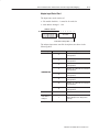
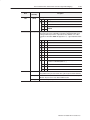
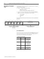
What this Manual Contains
The following table shows what each chapter of this manual
describes:
Chapter
Title
Describes
7(37,(8 1) " $0' #163
! '$25(3
18 1//60,&$5,10 $-(4 .$&(
$0' $22,0*
$&-2.$0( &1//60,&$5,10 %(58((0 5+( /1'6.(4
$0' 5+( $'$25(3 $0' +18 '$5$ ,4 /$22(' ,051 5+(
,/$*( 5$%.(
100(&5 5+( '$25(3 51 5+(
! (5813-
+( 2+:4,&$. .$:(3 +18 51 4(.(&5 5+( .,0( 5:2(
:16 4+16.' 64( $0' +18 51 &100(&5 51 $0'
5(3/,0$5( 5+( 0(5813-
10),*63( 5+( '$25(3 )13
$45(3.$7( 1//60,&$5,10
18 51 &10),*63( 5+( $'$25(3 )13 /$45(34.$7(
&1//60,&$5,10
316%.(4+115,0*
+( " 4:45(/ $0' ! $'$25(3
18 51 64( 5+( ,0',&$5134 )13 5316%.(4+115,0*
22(0',9 2(&,),&$5,104
'$25(3 42(&,),&$5,104
22(0',9 (7,&( $5$ $4( ,.(
(7,&( $5$ $4( ,.(
22(0',9 $;$3'164 1&$5,104
'(05,),&$5,10 1) +$;$3'164 3$5,0*4
6%.,&$5,10 <! 17(/%(3 P–2
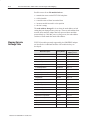
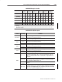
About this User Manual
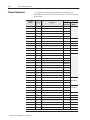
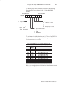
Related Publications
For additional information on planning and installing your
PROFIBUS system using FLEX I/O modules, refer to the following
publications:
Catalog
Number
Publications
Voltage
Description
# (&*/+&$- $5$
Installation
Instructions
User
Manual
9 9
" '&
0/530-(5 '$15(3
9
9
" '&
('6/'$/5 ('+$ 0/530-(5 '$15(3
9
9
" '&
0/530-(5 '$15(3
9
9
" '&
('6/'$/5 ('+$ 0/530-(5 '$15(3
9
9
" '&
(7+&((5 '$15(3
9
9!
9 " '&
(.05( '$15(3
9
9
9
" '&
(.05( '$15(3
9
9!
9
" '&
9-05 (.05( '$15(3
9
9!
9
" '&
! '$15(3
9
9
9
" '&
! '$15(3
9
9!
9
" '&
+/, /165 0'6-(
9
9
" '&
063&( 65165 0'6-(
9
9
" '&
+/, /165 0'6-(
9
9
" '&
+/, /165 0'6-(
9
9
" '&
063&( 65165 0'6-(
9
9"
" '&
063&( /165 0'6-(
9
9"
" '&
+/, 65165 0'6-(
9
9
" '&
-(&530/+&$--8 64(' 65165 0'6-(
9
9
" '&
(/403 /165 0'6-(
9#
" '&
/165 65165 0'6-(
9
9
" '&
(-(&5$%-( /$-0) /165 0'6-(
9
9
" '&
(-(&5$%-( /$-0) 65165 0'6-(
9
9
#
" '&
/165 65165 /$-0) 0'6-(
9
9
" '&
65165 40-$5(' /$-0) 0'6-(
9
9
" '&
/165 40-$5(' /$-0) 0'6-(
9
9#
" '&
/165 65165 40-$5(' /$-0) 0'6-(
9
9
" '&
/165 /$-0) 0'6-(
9
9!
9 " '&
*(3.0&061-( /165 0'6-(
9
9!
9 " '&
*(3.0&061-( /165 0'6-(
9
9!
9
" '&
3(26(/&8 /165 0'6-(
9
9!
9
" '&
*$//(- 3(26(/&8 /165 0'6-(
9
9!
9
" '&
*$//(- 6-4( 06/5(3 0'6-(
9
9!
9"
" '&
+)* 1((' 06/5(3 0'6-(
9
9!
Table continued on next page
6%-+&$5+0/ 9! 07(.%(3 9
9!
9!
About this User Manual
Publications
Catalog
Number
Voltage
5
#"
#" *,0/ +#0($
5
5
#"
#" 0/,0/ +#0($
5
5
"
*,0/ +#0($
5
5
"
0/,0/ +#0($
5
5
"
.+( /$# *,0/ +#0($
5
5
"
.+( /$# 0/,0/ +#0($
5
5
"
*,0/ +#0($
5
5
"
0/,0/ +#0($
5
5
"#"
*,0/ +#0($
5
"#"
0/,0/ +#0($
Description
Installation
Instructions
5
52'-$ $-)'* ( .$
52'-$ $-)'* ( .$
5
5
$-)'* ( .$ *'/
5
5
0.$# $-)'* ( .$ *'/
5
5
$),$- /0-$ $-)'* ( .$ *'/
5
5
,-'*& ( ), $-)'* ( .$ *'/
5
5
,-'*& ( ), $),$- /0-$ .$ *'/
5
5
$-)'* ( .$ *'/
5
5
,-'*& ( ), $-)'* ( .$ *'/
5
3/$*#$- !($.
5
+0*/'*& '/
5
5
User
Manual
5
5
5
5 5
P–3
5
#"
+2$- 0,,(4
5
5
#"
+2$- 0,,(4
5
5
#"
+2$- 0,,(4
5
To order these publications, contact your local Allen-Bradley
representative.
Conventions
+-$ *%+-) /'+*
This icon appears when more information is available in related
documentation.
0!('" /'+* 5 +1$)!$- P–4
About this User Manual
Table of Contents
Overview of FLEX I/O and
Your PROFIBUS Adapter
Module
Chapter 1
How Communication Takes
Place and I/O Image Table
Mapping
Chapter 2
#,%6 6,-5 ,%36)4 216%-15 ,) $ :56)0 2716 %1( )028) :274 :56)0 %5-/: 36-21%/ '')5524-)5 2716-1+ -6 ; 74325) 2* 6,) ; $ (%36)4 ! (%36)4 20321)165 -%+1256-' 1(-'%6245 )6924. 211)'624 )66-1+ 6,) 2() ((4)55 9-6',)5 29)4 #-4-1+ #,%6 6,-5 ,%36)4 216%-15 20071-'%6-21 8)4 6,) %'.3/%1) 2//)( 647'674) (%36)4 1376 6%675 #24( %33-1+ %6% -162 6,) 0%+) %&/) ; ;32-16 -+-6%/ 1376 2(7/) 0%+) %&/) %33-1+ ; )024: %3 ; ;32-16 -+-6%/ 1376 2(7/) 0%+) %&/) %33-1+ ; )024: %3 ; ;32-16 -5'4)6) 76376 2(7/) 0%+) %&/) %33-1+
; )024: %3 ; ;32-16 -5'4)6) 76376 2(7/) 0%+)
%&/) %33-1+ ; )024: %3 ;32-16 274') 1376 2(7/) 0%+) %&/) %33-1+ ;"
)024: %3 2* ;2-16 1376 2(7/) 0%+) %&/) ;" 1376 -/6)4 -0)5 *24 6,) ;" 1376 2(7/) ;32-16 -+-6%/ -1. 76376 2(7/) 0%+) %&/) %33-1+ ;" )024: %3 2* ;2-16 -+-6%/ -1. 76376 2(7/) 0%+) %&/) ;" ; ;32-16 -5'4)6) )1524 1376 2(7/) 0%+)
%&/) %33-1+ ; )024: %3 ; ;32-16 -5'4)6) 426)'6)( 76376 2(7/) 0%+) %&/)
%33-1+ ;32-16 -+-6%/ 137676376 2(7/) 0%+) %&/) %33-1+ ;$ 7&/-'%6-21 ! 28)0&)4 Table of Contents
(/138 $2 1) 91,05 ,*,5$. 026565265 1'6.( /$*( $%.( 9" 9 921,05 ,4&3(5( 0265 1'6.( /$*( $%.( $22,0* 9 (/138 $2 9 921,05 ,4&3(5( 65265 1'6.( /$*( $%.( $22,0* 9 (/138 $2 9! 921,05 ,4&3(5( (.$8 65265 1'6.( /$*(
$%.( $22,0* 9! (/138 $2 9 (3,(4 0265 0$.1* 1'6.( 9 (/138 $2 9 $0*( (.(&5,10 ,54 9 !13',5 (4&3,25,104 9 (3,(4 65265 0$.1* 1'6.( /$*(
$%.( $22,0* 9 (/138 $2 9 $0*( (.(&5,10 ,54 !3,5( !13' 9 !13',5 (4&3,25,104 9" (3,(4 0$.1* 1/%1 1'6.( /$*(
$%.( $22,0* 9" (/138 $2 9" $0*( (.(&5,10 ,54 9" !13',5 (4&3,25,104 9 0265 0$.1* 1'6.( /$*( $%.( $22,0* 9 ($' 9 !13',5 (4&3,25,104 9 +(3/1&162.( 0265 1'6.( /$*( $%.( $22,0* 9 ($' $0' !3,5( !13'4 9 !13',5 (4&3,25,104 +(3/1&162.( 0265 1'6.( 9 /$*(
$%.( $22,0* +(3/1&162.(/ 0265 1'6.( 9 ($' !13'4 ,5!13' (),0,5,104 )13 5+( .1&- 3$04)(3 !13'4 )13 5+( /
0265 1'6.( 0265 41.$5(' 0$.1* 1'6.( $5 1 9 /$*(
$%.( $22,0* 41.$5(' 0$.1* 0265 1'6.( 9 ($' (55,0* 5+( 0265 ,.5(3 10),*63,0* #163 0265 +$00(. !13',5 (4&3,25,104 )13 5+( 9 41.$5(' 0$.1*
0265 1'6.( 65265 41.$5(' 0$.1* 1'6.( 9 /$*(
$%.( $22,0* 41.$5(' 0$.1* 65265 1'6.( 9 ($' 10),*63,0* #163 652654 )13 5+( 9 41.$5(' 65265 1'6.( !13',5 (4&3,25,104 )13 5+( 9 41.$5(' 0$.1* 65265
1'6.( 6%.,&$5,10 17(/%(3 Table of Contents
630%7)( 2%03+ 31&3 3(80) ;# )5-)6 1%+)
%&0) %44-2+ 630%7)( 2%03+ 31&3 3(80) ;# )%( 32*-+85-2+ $385 2487 ,%22)06 )77-2+ 7,) 2487 -07)56 "35(-7 )6'5-47-326 *35 7,) ;# 2%03+
31&3 3(80) 2'5)1)27%0 2'3()5 3(80) ; 1%+) %&0) %44-2+ -7"35( )*-2-7-326 *35 03'/ 5%26*)5 )%( "35(6 *35 7,)
806) 3827)5 3(80) 806) 3827)5 3(80) ; 1%+) %&0) %44-2+ 03'/ 5%26*)5 "35( 66-+21)276 *35 7,) 806) 3827)5 3(80)
; -7"35( )*-2-7-326 *35 7,) 806) 3827)5 3(80) ; 4357 3(80) 1%+) %&0) %44-2+ 322)'7-32 7%786 "35( )*-2-7-32 3+-' 7%7862%03+ ))(&%'/ )*-2-7-32 322)'7-32 2%&0) "35( )*-2-7-32 3+-' 311%2(2%03+ )*)5)2') )*-2-7-32 Connect the Adapter to the
PROFIBUS DP Network
Chapter 3
Configure the Adapter for
Master/Slave Communication
Chapter 4
",%7 7,-6 ,%47)5 327%-26 %&0)6 ;.82'7-32 322)'7356 )51-2%7-32 03'/6 86 322)'735 %&0)6 ;.82'7-32 322)'7356 )51-2%7-32 03'/6 86 322)'735 322)'7 7,) (%47)5 73 7,) )7:35/ 322)'7 73 7,) (%47)5 )51-2%7) 7,) )7:35/ )51-2%7) %7 7,) (%47)5 !6-2+ -2) )51-2%7) %7 7,) (%47)5 !6-2+ -2) ",%7 7,-6 ,%47)5 327%-26 3: %67)50%9) 31182-'%7-32 %/)6 0%') 27)5-2+ !6)5 %5%1)7)5 %7% !6)5 %5%1)7)5 %7% 27)5-2+ ,)'/ 32*-+85%7-32 %7% )%( 32*-+85%7-32 )64326) %7% toc-iii
8&0-'%7-32 ! 39)1&)5 toc-iv
Table of Contents
Troubleshooting
Chapter 5
$- -$%, $*-!+ )(-%(, +).&!,$))-%(# 0%-$ -$! ( %-)+, %!0%(# --., "+)' -$! ,-!+, )("%#.+-%)( )"-0+! Specifications
Appendix A
*!%"%-%)(, Device Data Base File
.&%-%)( )/!'!+ Appendix C
1+ )., )-%)(, Glossary
Appendix B
!/%! - ,! %&! $- -$%, $*-!+ )(-%(, Hazardous Locations
Overview of FLEX I/O and Your
PROFIBUS Adapter Module
What this Chapter Contains
The FLEX I/O System
This chapter describes:
• what the FLEX I/O system is and what it contains
• how to mount and remove your system easily
• optional accessories
• mounting dimensions and spacing requirements
• the 1794-APB FLEX I/O PROFIBUS Adapter
• adapter components
• how to connect power wiring
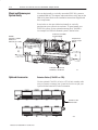
FLEX I/O is a small, modular I/O system for distributed
applications that performs all of the functions of rack-based I/O. The
FLEX I/O system contains the following components:
Terminal Base
Adapter
I/O Module
• PROFIBUS adapter/power supply – powers the internal logic for
as many as eight I/O modules
• terminal base – contains a terminal strip to terminate wiring for
two- or three-wire devices
• I/O module – contains the bus interface and circuitry needed to
perform specific functions related to your application
For information on how communication occurs over the FLEX I/O
system backplane, refer to Chapter 2.
1–2
Overview of FLEX I/O and Your PROFIBUS Adapter Module
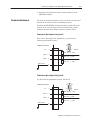
Mount and Remove your
System Easily
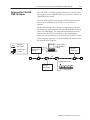
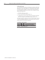
You can horizontally or vertically mount the FLEX I/O system on
a standard DIN rail. The adapter and terminal base easily snap on the
DIN rail by hand. Refer to the installation instructions shipped with
these components.
Screw holes are also provided to horizontally or vertically
panel-mount your system in an enclosure. To panel-mount your
FLEX I/O system, use the optional mounting kit (1794-NM1).
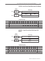
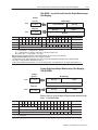
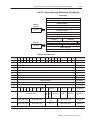
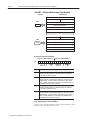
An example of a DIN rail-mounted system is shown below.
$&
2 *+- () 2
2
1 ''
+ 0 #)& , + /$&&
!)+ *( &2').(-$("
)'*)( (-, +
,&)-- -) *- +$&
)%$(" - )(( -)+ #)&,
- +'$(& , )(-) +$&
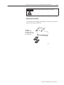
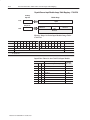
Optional Accessories
Extender Cables (1794ĆCE1 or ĆCE3)
Use the optional 1794-CE1 (0.3m) or -CE3 (0.9m) extender cable
(one per system) to arrange your system in two rows or split your
system into horizontal and vertical orientation.
2 )+ 2
1- ( + &
.&$-$)( 2 )/ ' + Overview of FLEX I/O and Your PROFIBUS Adapter Module
1–3
ATTENTION Do not use more than one cable per system.
!
Mounting Kit (1794ĆNM1)
Use the optional 1794-NM1 mounting kit to mount your system on a
panel or wall without a DIN rail.
(
%$ $ '$
#"'# #"'# "
$ !$" #"'#
" %
%$ (
&" 1–4
Overview of FLEX I/O and Your PROFIBUS Adapter Module
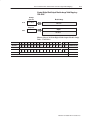
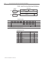
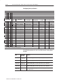
Mounting Dimensions
and Spacing Requirements
Inches
(Millimeters)
1794ĆAPB
6 6 6 6 A
/2).-!+
.3-2)-'
)2
1794ĆTB2, ĆTB3
6 6 6 6 !)+
C
%!130% (%0% &.0
4%02)#!+ ,.3-2)-'
/.1)2).- 5)2(
!$!/2%0 3/
B
%!130% (%0% &.0 (.0)8.-2!+
,.3.-2)-' /.1)2).-
Secure DIN Rail every 200mm.
.3-2)-' (.+% $),%-1).-1 &.0 ./2).-!+ ,.3-2)-' *)2 0!)+
/%0!2)-' 2%,/%0!230% "%+.5 %!#( ,.$3+% 5(%- ,.3-2%$ )- !-7 /.1)2).- -.2 2. %6#%%$ . .
3"+)#!2).- 9 .4%,"%0 //0.6),!2%+7
&.0
#!"+% .0
&.0
#!"+%
&0., 3//%0 #.--%#2.0
Overview of FLEX I/O and Your PROFIBUS Adapter Module
Purpose of the 1794ĆAPB
FLEX I/O Adapter
1–5
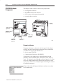
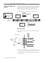
The 1794-APB is a FLEX I/O adapter that interacts with the FLEX
I/O backplane and any PROFIBUS DP master/scanner controller on
a PROFIBUS DP network.
The 1794-APB module is a slave device to the DP master/scanner,
and is a master controller of the FLEX I/O system where it is
installed.
The I/O data exchange occurs as follows: Output data is sent from
the DP master/scanner controller across the PROFIBUS DP network
to the 1794-APB adapter. The adapter then automatically transfers
the data across the FLEX I/O backplane to the output modules.
Inputs from the input modules are collected by the FLEX I/O adapter
via the backplane and sent across the PROFIBUS DP network to the
DP master/scanner controller.
.,- )"
1/ "$*"+0
".*&+0&,+ ), (
'1+ 0&,+
/0". ++".
,+0.,))".
"./,+) ,*-10".
3&0% ,+#&$1.0&,+
,#03."
5
0%". !-0".)2"
5 !-0". )2"
0%". !-0".)2"
4/0"*
1)& 0&,+ 5
,2"*". 1–6
Overview of FLEX I/O and Your PROFIBUS Adapter Module
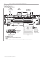
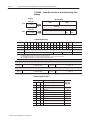
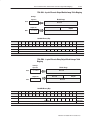
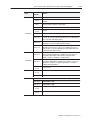
PROFIBUS Adapter
Components
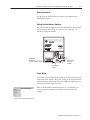
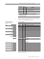
The adapter module consists of the following components:
•
•
•
•
two diagnostic indicators
PROFIBUS DP network connector
24V dc power wiring connection terminals
two node address switches
)#3 0.
,++#!/, '+"'!/,%-##+-#"
'+"'!/,%-##+-#"
"! 2'-'+%
,++#!/',+
#-*'+).
#/2,-(
,++#!/,-
,"# ""-#..
2'/!&#.
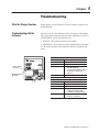
Diagnostic Indicators
Diagnostic indicators are located on the front panel of the adapter
module. They show both normal operation and error conditions in
your FLEX I/O system. The indicators are:
• Device status (STATUS)
• Communication link status (PROFIBUS)
Upon power-up, the adapter goes to an initialization state and
performs a self-test (memory check, data memory clear, CRC on
code). The indicators also go through a self-test sequence. If a failure
occurs, the adapter transitions to a faulted state and waits for reset
(cycle power). Otherwise, the adapter begins monitoring the network
(run state) for messages.
,-# +$,-*/',+
0 )'!/',+ 4 ,1#* #- Chapter 5 describes the diagnostic indicators and how to use them
for troubleshooting.
Overview of FLEX I/O and Your PROFIBUS Adapter Module
1–7
Network Connector
Use the 9-pin D-shell connector to connect your adapter to the
PROFIBUS network.
Setting the Node Address Switches
Set the node address using the 2-position thumbwheel switch. Valid
settings range from 01 to 99. Use a pen to press either the + or –
buttons to change the number.
24V DC
Adapter
1794-APB/B
!.1*,&
*))!.*, 2+%) 2-$!''
1%,%)#
*))!.%*)
!,(%)'* ! ,!-1%.$!-
Power Wiring
Connections are provided for connecting the required 24V dc power
to the front of the module. The power wiring can be daisy-chained to
the terminal base unit located next to the adapter to supply power to
the module installed in that base unit.
*,! )"*,(.%*)
Refer to the Installation Instructions (pub. no. 1794-IN040) you
received with your adapter to learn how to install and wire the
adapter.
/'%.%*) 2
*0!(!, 1–8
Overview of FLEX I/O and Your PROFIBUS Adapter Module
Chapter
2
How Communication Takes
Place and I/O Image Table
Mapping
What this Chapter Contains
Communication Over
the I/O Backplane
In this chapter, you will learn about:
• communication over the FLEX I/O backplane (between the
PROFIBUS adapter and the I/O modules)
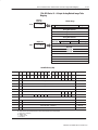
• how data is mapped into the I/O image table
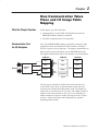
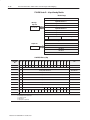
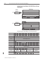
One 1794-APB PROFIBUS adapter can interface with up to eight
terminal base units with installed FLEX I/O modules, forming a
FLEX I/O system of up to eight slots. The adapter communicates to
other network system components over the PROFIBUS network.
The adapter communicates with its I/O modules over the backplane.
I/O Module
"$('&
Network
$'%
%'
I/O Module
#%&
''(&
('$('&
#"(%'#"
Slot 1
%'
#%&
I/O Module
"$('&
"$('&
''(&
''(&
('$('&
('$('&
#"(%'#"
#"(%'#"
Slot 2
Slot 8
The I/O map for a module is divided into read words and write
words. Read words consist of input and status words, and write
words consist of output and configuration words. The number of
read words or write words can be 0 or more. The length of each I/O
module’s read words and write words vary in size depending on
module complexity. Each I/O module will support at least 1 input
word or 1 output word. Status and configuration are optional,
depending on the module.
( '#" * #)!% 2–2
How Communication Takes Place and I/O Image Table Mapping
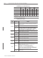
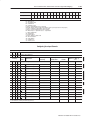
For example, a 16 point discrete input module will have up to 2 read
words and 1 write word.
I/O Image
Input Size
$& $&'
,%$ #( '&( #%)( $)!
Output Size
$& $&
Module Image
Inputs
Not used
Not used
!+
"
!+
"
Check the I/O map for each module for the exact mapping.
Polled I/O Structure
The first word of output data received by the adapter is the Adapter
Status Word. Output data is received by the adapter in the order of
the installed I/O modules. The Output data for Slot 1 is received
first, followed by the Output data for Slot 2, and so on up to slot 8.
All bits in the output status word are reserved
The first word of input data sent by the adapter is the Adapter Status
Word. This is followed by the input data from each slot, in the order
of the installed I/O modules. The Input data from Slot 1 is first after
the status word, followed by Input data from Slot 2, and so on up to
slot 8.
PROFIBUS Adapter
Read Data
%(& (()'
!$( #%)( (
Network READ
!$( #%)( (
!$( #%)( (
Write Data
& (
%(& (()'
Network WRITE
!$( )(%)( (
!$( )(%)( (
!$( )(%)( (
)! ( $# ,
$*"& I/O Module I/O Module
Slot 1
Slot 2
I/O Module
Slot 8
How Communication Takes Place and I/O Image Table Mapping
2–3
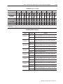
Adapter Input Status Word
The input status word consists of:
• I/O module fault bits – 1 status bit for each slot
• node address changed – 1 bit
+#0($ 0(/ '/.
(+/
(+/
(+/
(+/
(+/
(+/
(+/
(+/
'/
$.$-1$#
+#$ ##-$.. & *%$# '/
The adapter input status word bit descriptions are shown in the
following table.
Bit Description
Bit
Explanation
&'. !'/ '. .$/ 2&$* * $--+- '. #$/$"/$#
'* .(+/ ,+.'/'+* &'. !'/ '. .$/ 2&$* * $--+- '. #$/$"/$#
'* .(+/ ,+.'/'+* &'. !'/ '. .$/ 2&$* * $--+- '. #$/$"/$#
'* .(+/ ,+.'/'+* &'. !'/ '. .$/ 2&$* * $--+- '. #$/$"/$#
'* .(+/ ,+.'/'+* &'. !'/ '. .$/ 2&$* * $--+- '. #$/$"/$#
'* .(+/ ,+.'/'+* &'. !'/ '. .$/ 2&$* * $--+- '. #$/$"/$#
'* .(+/ ,+.'/'+* &'. !'/ '. .$/ 2&$* * $--+- '. #$/$"/$#
'* .(+/ ,+.'/'+* &'. !'/ '. .$/ 2&$* * $--+- '. #$/$"/$#
'* .(+/ ,+.'/'+* $.$-1$#
+#0($ 0(/
$.$-1$#
+#$ ##-$..
& *%$#
&'. !'/ '. .$/ 2&$* /&$ *+#$ ##-$..
.2'/"& .$//'*% & . !$$* "& *%$# .'*"$
,+2$- 0,
0!('" /'+* 3 +1$)!$- 2–4
How Communication Takes Place and I/O Image Table Mapping
Possible causes for an I/O module fault are:
•
•
•
•
•
transmission errors on the FLEX I/O backplane
a failed module
a module removed from its terminal base
incorrect module inserted in a slot position
the slot is empty
The node address changed bit is set when the node address switch
setting has been changed since power up. The new node address does
not take effect until the adapter has been powered down and then
powered back up. Until this power cycling occurs, the node address
switches will not match the actual node address.
Mapping Data into
the Image Table
FLEX I/O modules presently supported by the PROFIBUS adapter
are listed below. Additional modules will be added as they are
developed.
Module Description
1!)'" 0',+ 4 ,2$*!$. Catalog Number
For image table
mapping, refer to:
'+( +-10 ,#1)$
4
- %$ '+( +-10 ,#1)$
4
- %$ ,1."$ 10-10 ,#1)$
4
- %$ ,1."$ 10-10 ,#1)$
4
- %$ ,1."$ +-10 ,#1)$
4
- %$ '+( 10-10 ,#1)$
4
- %$ $+/,. +-10 ,#1)$
4
- %$ )$"0.,+'" ))3 1/$# 10-10 ,#1)$
4
- %$ +-10
10-10 ,#1)$
4
- %$ +-10 ,#1)$
4
- %$ 10-10 ,#1)$
4
- %$ $) 3 10-10 ,#1)$
4
- %$ +-10 + ),% ,#1)$
4
- %$ 10-10 + ),% ,#1)$
4
- %$ '+ ,10 + ),% ,*!, ,#1)$
4
- %$ +-10 + ),% ,#1)$
4
- %$ +-10 &$.*,",1-)$ ,#1)$
4
- %$ +-10 &$.*,",1-)$* ,#1)$
4
- %$ +-10 1)/$ ,1+0$. ,#1)$
- %$ +-10 +",#$. ,1+0$. ,#1)$
- %$ -,.0 ,#1)$
4
- %$ How Communication Takes Place and I/O Image Table Mapping
2–5
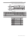
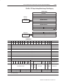
1794ĆIB8 - 8Ćpoint Digital Input Module Image Table Mapping
I/O Image
Module Image
Input Size
Read
Not used
)+ )+!,
Inputs
Not used
Output Size
Write
%&-"+
%'"
Not used
)+ )+!
1794ĆIB8 Memory Map
Decimal Bit
15
14
13
12
11
10
09
08
07
06
05
04
03
02
01
00
Size
Octal Bit
17
16
15
14
13
12
11
10
07
06
05
04
03
02
01
00
Read Words
"! )+! )- .,"!
Not used
"! )+! Not used
$"+"
+%-" )+! (*.- - )++",*)(!, -) %(*.- )++",*)(!, -) %(*.- "- (*.- %&-"+ %'" )++",*)(!, -) %(*.-, -$+. 1794ĆIB8 Input Filter Times
Bits
Description
Selected
Filter Time
02
01
00
Filter Time for Inputs 00-07
%&-"+ %'" !"#.&-
%&-"+ %'" ',
%&-"+ %'" ',
%&-"+ %'" ',
%&-"+ %'" ',
%&-"+ %'" ',
%&-"+ %'" ',
%&-"+ %'" ',
µ,
.&% -%)( 0 )/"'"+ 2–6
How Communication Takes Place and I/O Image Table Mapping
1794ĆIB16 - 16Ćpoint Digital Input Module Image Table Mapping
I/O Image
Module Image
Input Size
Read
Inputs
*, *,"-
Not used
Output Size
Write
&'.#,
&(#
Not used
*, *,"
&'.#,
&(#
1794ĆIB16 Memory Map
Decimal Bit
15
14
13
12
11
10
09
08
07
06
05
04
03
02
01
00
Size
Octal Bit
17
16
15
14
13
12
11
10
07
06
05
04
03
02
01
00
Read Words
#" *," Not used
#" *," Not used
%#,#
)+/. . !*,,#-+*)"- .* &)+/. !*,,#-+*)"- .* &)+/. #.!
)+/. &'.#, &(# !*,,#-+*)"- .* &)+/.- .%,/ !*,,#-+*)"- .* &)+/.- .%,/ 1794ĆIB16 Input Delay Times
Bits
/ '&!.&*) 1 *0#( #, Description
S
Selected
Filter Time
02
01
00
Filter Time for Inputs 00-11
05
04
03
Filter Time for Inputs 12-15
&'.#, &(# "#$/'.
&'.#, &(# (-
&'.#, &(# (-
&'.#, &(# (-
&'.#, &(# (-
&'.#, &(# (-
&'.#, &(# (-
&'.#, &(# (-
µ-
,&.# *," How Communication Takes Place and I/O Image Table Mapping
2–7
1794ĆOB8 - 8Ćpoint Discrete Output Module Image Table Mapping
I/O Image
Input Size
Read
Module Image
%' %'
Not used
Output Size
Not used
Outputs
%' %'(
Write
Not used
1794ĆOB8 Memory Map
Decimal Bit
15
14
13
12
11
10
09
08
07
06
05
04
03
02
01
00
Octal. Bit
17
16
15
14
13
12
11
10
07
06
05
04
03
02
01
00
Size
Read Words
Not used
%) *(
%' Not used
'
'!) %' '!) %' *)&*) +"* %''(&%$( )% %*)&*) %''(&%$( )% %*)&*) )
1794ĆOB16 - 16Ćpoint Discrete Output Module Image Table
Mapping
I/O Image
Input Size
Read
Module Image
%' %'
Not used
Output Size
Outputs
%' %'(
Write
Not used
1794ĆOB16 Memory Map
Dec. Bit
15
14
13
12
11
10
09
08
07
06
05
04
03
02
01
00
Size
Oct. Bit
17
16
15
14
13
12
11
10
07
06
05
04
03
02
01
00
Read/Write Words
Not used
Not used
'
%' '!) %' '!) %' *)&*) +"* %''(&%$( )% %*)&*) %''(&%$( )% %*)&*) )
*"!)!%$ , %+#' 2–8
How Communication Takes Place and I/O Image Table Mapping
16Ćpoint Source Input Module Image Table Mapping - 1794ĆIV16
I/O Image
Input Size
Read
Module Image
') ')
Inputs
Output Size
Write
$/
#%
Not used
Not used
') ')*
Not used
Memory Map of 16-Point Input Module Image Table –
1794-IV16
Dec. Bits
Oct. Bits
15
14
13
12
11
10
09
08
07
06
05
04
03
02
01
00
Size
17
16
15
14
13
12
11
10
07
06
05
04
03
02
01
00
Read/Write Words
.') Not used
!') $$ "&& $*
Not used
Not used
" )
)#+ .') )#+ .') &(,+ +
&(,+ !#$+ ) #%
Input Filter Times for the 1794-IV16 Input Module
Bits
,$#+#'& 0
'- % ) Description
Selected
Filter Time
10
09
08
Filter Time for Inputs 00-15 (00-17)
#$+ ) #% !,$+
µ*
#$+ ) #% µ*
#$+ ) #% %*
#$+ ) #% %*
#$+ ) #% %*
#$+ ) #% %*
#$+ ) #% %*
#$+ ) #% %*
How Communication Takes Place and I/O Image Table Mapping
2–9
16Ćpoint Digital Sink Output Module Image Table Mapping 1794ĆOV16
I/O Image
Input Size
Read
Module Image
!# !#
Not used
Output Size
Outputs
!# !#$
Write
Not used
Memory Map of 16-Point Digital Sink Output Module Image
Table – 1794-OV16
Dec. Bits
15
14
13
12
11
10
09
08
07
06
05
04
03
02
01
00
Size
Oct. Bits
17
16
15
14
13
12
11
10
07
06
05
04
03
02
01
00
Read/Write Words
(!# !% &$
!% &$
#
#% (!# #% (!# &%"&% '&
&%! )
!'# 2–10
How Communication Takes Place and I/O Image Table Mapping
1794ĆIB8S - 8Ćpoint Discrete Sensor Input Module Image Table
Mapping
I/O Image
Module Image
Input Size
Read
Status
,. ,.#/
Inputs
Not used
Output Size
Write
$) 4
(*$
Not used
,. ,.#
$) 4
(*$
1794ĆIB8S Memory Map
Decimal Bit
15
14
13
12
11
10
09
08
07
06
05
04
03
02
01
00
Size
Octal Bit
17
16
15
14
13
12
11
10
07
06
05
04
03
02
01
00
Read Words
$ # ,.# Not used
$ # ,.# Not used
'$.$
0 01/ ,% (+-10 3'$.$ ",..$/-,+#/ 0, 0'$ #( &+,/0(" !(0 %,. (+-10 ",..$/-,+#/ 0, 0'$ #( &+,/0(" !(0 %,. (+-10 $0"
+-10 0 3'$.$ ",..$/-,+#/ 0, (+-10 ",..$/-,+#/ 0, (+-10 $0"
+-10 $) 4 (*$ 3'$.$ ",..$/-,+#/ 0, (+-10/ 0'.1 ",..$/-,+#/ 0, (+-10/ 0'.1 Make certain that the delay time for 00-11 is the same as the delay time for 12-15.
Smart Sensor
(0/
( &+,/0(" # 0 1)0 -.$/$+0 * .0
,.* ) +, $..,./
(0/
+-10 # 0
$+/,. ,+
$+/,. ,%%
( &+,/0("/ +,0 #(/ !)$#
,.* ) (/ !)$#
(0/
+-10 # 0
$+/,. ,+
$+/,. ,%%
Standard Sensor
(0/
( &+,/0(" # 0 1794ĆIB8S Input Delay Times
Bits
1!)(" 0(,+ 5 ,2$*!$. Description
S
Selected
Delayy Time
02
01
00
Delay Time for Inputs 00-11
05
04
03
Delay Time for Inputs 12-15
$) 4 (*$ #$% 1)0
$) 4 (*$ */
$) 4 (*$ */
$) 4 (*$ */
$) 4 (*$ */
$) 4 (*$ */
$) 4 (*$ */
$) 4 (*$ */
µ/
.(0$ ,.# How Communication Takes Place and I/O Image Table Mapping
2–11
1794ĆOB8EP - 8Ćpoint Discrete Protected Output Module Image
Table Mapping
I/O Image
Input Size
Read
Module Image
.0 !.0%
Overload Fault Bits
Output Size
Not used
Outputs
.0 !.0%1
Write
Not used
Not used
Dec. Bits
15
14
13
12
11
10
09
08
07
06
05
04
03
02
01
00
Size
Oct. Bits
17
16
15
14
13
12
11
10
07
06
05
04
03
02
01
00
Read/Write Words
.2 31&%
&1&04&%
&1&04&% 1&& -.2&
&"% !0*2& !0*2& !)&0&
.4&0+."% '"3+2 #*21 '"3+2 /0&1&-2 -. '"3+2
.32/32 %"2" $.00&1/.-%1 2. .32/32 $.00&1/.-%1 2. .32/32 &2$
'"3+2 0&1&2 #*2 0&1&2 .32/32 -. $)"-(&
Note: )& 3-31&% +.5&0 #72& *- 0&"% 5.0% '+."21 %30*-( ./&0"2*.- . -.2 31& 2)*1 #72& '.0 '"3+2 12"231
Using the Fault Reset Button !)&- 7.3 /0&11 2)& ,"-3"+ 0&1&2 #322.-
2)& '"3+2 *-%*$"2.0 '.0 2)& '"3+2&% .32/32 230-1 .'' '.0 "#.32 1 2)& '"3+2&% .32/32 5*++ -.2 "22&,/2 2. 230- .- %30*-( 2)*1 %&+"7
"'2&0 2)& 1 %&+"7 2)& '"3+2&% .32/32 "22&,/21 2. 230- .
*' 2)& &62&0-"+ $.-%*2*.- $"31*-( 2)& '"3+2 *1 $.00&$2&% 2)& .32/32 0&,"*-1 .- 2)& '"3+2 *-%*$"2.0 *1 .'' "-% 2)& 12"231 *-%*$"2.0 *1 .-
16Ćpoint Digital Input/Output Module Image Table Mapping 1794ĆIB10XOB6
I/O Image
Module Image
Input Size
Not used
.0 !.0%1
Read
Inputs
Not used
Output Size
Write
Not used
.0 !.0%
Outputs
Memory Map of 16-Point Digital Input/Output Module Image
Table – 1794-IB10XOB6
Dec. Bits
15
14
13
12
11
10
09
08
07
06
05
04
03
02
01
00
Size
Oct. Bits
17
16
15
14
13
12
11
10
07
06
05
04
03
02
01
00
Read/Write Words
&"% 5.0% .2 31&%
Not used
.2 31&%
!)&0&
&"% 5.0% !0*2& 5.0% -/32 )"--&+
32/32 )"--&+
3#+*$"2*.- 8 .4&,#&0 2–12
How Communication Takes Place and I/O Image Table Mapping
1794ĆIA8 - 8Ćpoint Discrete Input Module Image Table Mapping
Module Image
I/O Image
Input Size
Read
Not used
)+ )+!,
Inputs
Not used
Output Size
Write
%&-"+
%'"
Not used
)+ )+!
1794ĆIA8 Memory Map
Decimal Bit
15
14
13
Octal Bit
17
16
15
12
11
10
09
08
14
13
12
11
10
Not used
07
06
05
04
03
02
01
00
07
06
05
04
03
02
01
00
Read Words
"! )+! Not used
"! )+! Not used
$"+"
Size
+%-" )+! (*.- - 0$"+" )++",*)(!, -) %(*.- )++",*)(!, -) %(*.- "- (*.- %&-"+ %'" 0$"+" )++",*)(!, -) %(*.-, -$+. 1794ĆIA8 Input Filter Times
Bits
.&% -%)( 1 )/"'"+ Description
02
01
00
Filter Time for Inputs 00-07
%&-"+ %'" !"#.&-
%&-"+ %'" Maximum Filter Time
Off to On
On to Off
',
',
',
',
%&-"+ %'" ',
',
%&-"+ %'" ',
',
%&-"+ %'" ',
',
%&-"+ %'" ',
',
%&-"+ %'" ',
',
%&-"+ %'" ',
',
How Communication Takes Place and I/O Image Table Mapping
2–13
1794ĆOA8 - 8Ćpoint Discrete Output Module Image Table Mapping
I/O Image
Module Image
Input Size
') ')
Read
Not used
Output Size
Write
Not used
') ')*
Outputs
Not used
1794ĆOA8 Memory Map
Decimal Bit
15
14
13
12
11
10
09
08
07
06
05
04
03
02
01
00
Oct. Bit
17
16
15
14
13
12
11
10
07
06
05
04
03
02
01
00
Not used
'+ ,* Read Words
') Not used
" )
Size
)#+ ') )#+ ') ,+(,+ -$, ." ) ')) *('&* +' ',+(,+ ')) *('&* +' ',+(,+ +
1794ĆOW8 - 8Ćpoint Discrete Relay Output Module Image Table
Mapping
I/O Image
Read
Input Size
Module Image
') ')
Not used
Output Size
Not used
Outputs
') ')*
Write
Not used
1794ĆOW8 Memory Map
Decimal Bit
15
14
13
12
11
10
09
08
07
06
05
04
03
02
01
00
Size
Oct. Bit
17
16
15
14
13
12
11
10
07
06
05
04
03
02
01
00
Read Words
Not used
'+ ,* ') Not used
" )
)#+ ') )#+ ') ,+(,+ -$, ." ) ')) *('&* +' ',+(,+ ')) *('&* +' ',+(,+ + & ." & #+ +" ',+(,+ #* '!! ." & #+ +" ',+(,+ #* '&
,$#+#'& / '- % ) 2–14
How Communication Takes Place and I/O Image Table Mapping
1794ĆIE8 Series B - 8 Input Analog Module
Module Image
Input Data Channel 0
Input Data Channel 1
I/O Image
Input Data Channel 2
Input Size
Input Data Channel 3
Input Data Channel 4
0, ,.#/
Input Data Channel 5
Input Data Channel 6
Input Data Channel 7
Underrange
PU
Configure select
Not used
Output Size
Not used
,. ,.#
Not used
Not used
Not used
1794ĆIE8/B Memory Map
Decimal
Bit
15
14
13
12
11
10
09
08
07
06
05
04
03
02
01
00
Size
Oct. Bit
17
16
15
14
13
12
11
10
07
06
05
04
03
02
01
00
Read/Write Words
+ ),& )1$ ' ++$) $ # ,.# + ),& )1$ ' ++$) $ # ,.# + ),& )1$ ' ++$) $ # ,.# + ),& )1$ ' ++$) $ # ,.# + ),& )1$ ' ++$) $ # ,.# + ),& )1$ ' ++$) $ # ,.# + ),& )1$ ' ++$) $ # ,.# + ),& )1$ ' ++$) $ # ,.# ,0 1/$# /$0 0, 5$.,
$ # ,.# .(0$ ,.# ,0 1/$# /$0 0, '$.$
,3$. 1- !(0 (+")1#$# (+ /$.($/ *,#1)$/ ,+)4
+#$.. +&$ !(0/ %,. 6* (+-10/
,+%(&1.$ /$)$"0 !(0
1)) . +&$ !(0
/(&+ !(0 (+ / ",*-)$*$+0
1!)(" 0(,+ 6 ,2$*!$. .(0$ ,.# 0'.1 How Communication Takes Place and I/O Image Table Mapping
2–15
1794ĆIE8/B Range Selection Bits
Channel No.
Channel 0
Channel 1
Channel 2
Channel 3
Channel 4
Channel 5
Channel 6
Channel 7
F0
C0
F1
C1
F2
C2
F3
C3
F4
C4
F5
C5
F6
C6
F7
C7
Decimal Bits
(Octal Bits)
00
08
(10)
01
09
(11)
02
10
(12)
03
11
(13)
04
12
(14)
05
13
(15)
06
14
(16)
07
15
(17)
! &%
.
.
9 40 ! &%
((
0/(+)52' 3'-'%4 $+4
5-- 2#/)' $+4
"*'/ %0/(+)52'& 40 0(( +/&+6+&5#- %*#//'-3 7+-- 2'452/ 0/ '2+'3 .0&5-'3 #/& 40 . 0/ '2+'3 .0&5-'3
1794ĆIE8 Word/Bit Descriptions
Word
'#& "02& Decimal Bit
Definition
+43 Channel 0 analog data 9$+4 -'(4 ,534+(+'& 4703 %0.1-'.'/4
/5.$'2 5/53'& -07'2 $+43 #2' 8'20 9
. 53'3 #-- $+43
+43 '#& "02& +43 +43 '#& "02& +43 +43 '#& "02& +43 +43 '#& "02& +43 +43 '#& "02& +43 +43 '#& "02& +43 +43 '#& "02& +43 +43 *#//'- #/#-0) # 3+)/ $+4
Channel 1 analog data 9$+4 -'(4 ,534+(+'& 4703 %0.1-'.'/4
/5.$'2 5/53'& -07'2 $+43 #2' 8'20 9
. 53'3 #-- $+43
*#//'- #/#-0) # 3+)/ $+4
Channel 2 analog data 9$+4 -'(4 ,534+(+'& 4703 %0.1-'.'/4
/5.$'2 5/53'& -07'2 $+43 #2' 8'20 9
. 53'3 #-- $+43
*#//'- #/#-0) # 3+)/ $+4
Channel 3 analog data 9$+4 -'(4 ,534+(+'& 4703 %0.1-'.'/4
/5.$'2 5/53'& -07'2 $+43 #2' 8'20 9
. 53'3 #-- $+43
*#//'- #/#-0) # 3+)/ $+4
Channel 4 analog data 9$+4 -'(4 ,534+(+'& 4703 %0.1-'.'/4
/5.$'2 5/53'& -07'2 $+43 #2' 8'20 9
. 53'3 #-- $+43
*#//'- #/#-0) # 3+)/ $+4
Channel 5 analog data 9$+4 -'(4 ,534+(+'& 4703 %0.1-'.'/4
/5.$'2 5/53'& -07'2 $+43 #2' 8'20 9
. 53'3 #-- $+43
*#//'- #/#-0) # 3+)/ $+4
Channel 6 analog data 9$+4 -'(4 ,534+(+'& 4703 %0.1-'.'/4
/5.$'2 5/53'& -07'2 $+43 #2' 8'20 9
. 53'3 #-- $+43
*#//'- #/#-0) # 3+)/ $+4
Channel 7 analog data 9$+4 -'(4 ,534+(+'& 4703 %0.1-'.'/4
/5.$'2 5/53'& -07'2 $+43 #2' 8'20 9
. 53'3 #-- $+43
*#//'- #/#-0) # 3+)/ $+4
5$-+%#4+0/ 9 06'.$'2 2–16
How Communication Takes Place and I/O Image Table Mapping
Word
(* Decimal Bit
Definition
#,+ Underrange bits (U) (* #'#.#-% "''%+ (4Ć20mA current
input only) #, (**+)('+ ,( #')-, "''% #, (**+)('+ ,( #')-, "''% ' +( (' "' +, #'#,+ #,"* *($' (* ()' #')-, /#* (* #')-, -**',
%(/ 2&
#,+ 2
(, -+ +, ,( #, Power Up bit - included in series B modules only. This bit
is 0 in series A modules. This bit is set to 1 when all bits in
the configuration register are 0 (unconfigured state). "
(' #!-*,#(' *!#+,* ' %* 0 #,"* ( ," *+,
#')-,+ (* 0 ," -+* /*#,#'! %% 1*(+ ,( #,
#,+ Full range bits (F) (* #'#.#-% "''%+ #, (**+)('+
,( #')-, "''% #, (**+)('+ ,( #')-, "''% '
+( (' * ,( *'! +%,#(' (.
#,+ Configure select bits (C) (* #'#.#-% "''%+ #, (**+)('+ ,( #')-, "''% #, (**+)('+ ,( #')-,
"''% ' +( (' * ,( *'! +%,#(' (.
*#, (* #,+ (, -+ +, ,( *#, (* #,+ (, -+ +, ,( *#, (* #,+ (, -+ +, ,( *#, (* #,+ (, -+ +, ,( *#, (* #,+ (, -+ +, ,( *#, (* -%#,#(' 2 (.&* How Communication Takes Place and I/O Image Table Mapping
2–17
1794ĆOE4 Series B - 4 Output Analog Module Image Table
Mapping
I/O Image
Input Size
Module Image
-/ -/#
Read
PU
Diagnostics
Not used
Analog Data Channel 0
Analog Data Channel 1
Analog Data Channel 2
Analog Data Channel 3
Not used
Output Size
Write
MC
Full Range
Config. Select
Not used
Not used
Not used
-/ -/#0
Not used
Not used
Not used
Safe State Value - Channel 0
Safe State Value - Channel 1
Safe State Value - Channel 2
Safe State Value - Channel 3
1794ĆOE4 Memory Map
Dec. Bit
15
14
13
12
11
10
09
08
07
06
05
04
03
02
01
00
Size
Octal Bit
17
16
15
14
13
12
11
10
07
06
05
04
03
02
01
00
Read/Write Words
$ # -/# -1 20$# 0$1 1- 7$/-
, *-& 1 ' ,,$* /(1$ -/# , *-& 1 ' ,,$* -/# , *-& 1 ' ,,$* -/# , *-& 1 ' ,,$* -/# -1 20$# 0$1 1- -1 20$# 0$1 1- -1 20$# 0$1 1- -1 20$# 0$1 1- '$/$
-/# -/# -/# 1'/2 %$ 1 1$ *2$ ' ,,$* -/# %$ 1 1$ *2$ ' ,,$* -/# %$ 1 1$ *2$ ' ,,$* -/# %$ 1 1$ *2$ ' ,,$* -/# -4$/ 2. !(1 (,"*2#$# (, 0$/($0 +-#2*$0 -,*6
( &,-01(" !(10 %-/ "2//$,1 -21.21 4(/$ !/-)$, -/ *- # /$0(01 ,"$ '(&' -1 20$# -, 3-*1 &$ -21.210
(&, !(1 (, 0 "-+.*$+$,1
2*1(.*$5 "-,1/-*
-,%(&2/$ 0$*$"1 !(1
2** / ,&$ !(1
2!*(" 1(-, 8 -3$+!$/ 2–18
How Communication Takes Place and I/O Image Table Mapping
1794ĆOE4/B Range Selection Bits (Write Word 6)
Channel No.
Channel 0
Channel 1
Channel 2
Channel 3
F0
C0
F1
C1
F2
C2
F3
C3
Decimal Bit
00
08
01
09
02
10
03
11
/
! &%
/
;
51 ! &%
((
10(+)63' 4'.'%5 $+5
6.. 3#0)' $+5
"*'0 %10(+)63'& 51 1(( +0&+7+&6#. %*#00'.4 8+.. 3'5630 !
1794ĆOE4 Word/Bit Descriptions
Word
Decimal Bit
(Octal Bit)
Definition
+54 ;
633'05 1652654 10.9 "*'0 4'5 5*' 8+3' 10 5*' 165265 +4 $31-'0 13 5*' .1#&
3'4+45#0%' +4 511 *+)* +5 %133'4210&4 51 %*#00'. $+5 %133'4210&4 51
%*#00'. #0& 41 10
+54 ;
15 64'& 4'5 51 +5 Power Up bit - included in series B modules only. This bit is always 0 in
series A modules. This bit is set to 1 when all bits in the configuration
register (write word 5) are 0 (unconfigured state). *' %10(+)63#5+10 3')+45'3
%#0 $' %.'#3'& $9 '+5*'3 # 3'4'5 13 $9 5*' 64'3 83+5+0) #.. :'31'4 51 +5
+54 Channel 0 analog data ;$+5 .'(5 ,645+(+'& 5814 %1/2.'/'05 06/$'3 6064'&
.18'3 $+54 #3' :'31 ;
/ 64'4 #.. $+54
+54 Channel 0 analog data sign bit.
+54 Channel 1 analog data ;$+5 .'(5 ,645+(+'& 5814 %1/2.'/'05 06/$'3 6064'&
.18'3 $+54 #3' :'31 ;
/ 64'4 #.. $+54
+54 Channel 1 analog data sign bit.
+54 Channel 2 analog data ;$+5 .'(5 ,645+(+'& 5814 %1/2.'/'05 06/$'3 6064'&
.18'3 $+54 #3' :'31 ;
/ 64'4 #.. $+54
+54 Channel 2 analog data sign bit.
+54 Channel 3 analog data ;$+5 .'(5 ,645+(+'& 5814 %1/2.'/'05 06/$'3 6064'&
.18'3 $+54 #3' :'31 ;
/ 64'4 #.. $+54
+54 Channel 3 analog data sign bit.
+54 Multiplex control bits (M (13 +0&+7+&6#. %*#00'.4 *'4' $+54 %10531. 5*' 4#('
45#5' #0#.1) 1652654 +5 %133'4210&4 51 165265 %*#00'. $+5 %133'4210&4 51 165265 %*#00'. #0& 41 10
64' 813&4 13 #4 &+3'%5'& $9 %*#00'. 06/$'3 0
64' 813&4 13 #4 &+3'%5'& $9 %*#00'. 06/$'3 0
"*'0 $+54 ;
#3' #.. %.'#3'& 4+/6.5#0'164.9 $9 # %1//60+%#5+10 '3313 13
64'3 %*1+%' 5*36 5*' 231)3#//#$.' %10531..'3 231)3#/ 813& (6.. 3#0)' #0&
%10(+)63' 4'.'%5 $+54 #3' 23'4'37'& #5 5*'+3 .#45 4'55+0)
+54 ;
;
15 64'& 4'5 51 '#& "13& "3+5' "13& "13& "13& "13& "13& 6$.+%#5+10 ; 17'/$'3 How Communication Takes Place and I/O Image Table Mapping
2–19
Decimal Bit
(Octal Bit)
Definition
"+* Full range bits (F) ') "&"-",$ !&&$* "+ '))*('&* +' ',+(,+ !&&$
"+ '))*('&* +' ',+(,+ !&&$ & *' '&
"+* 0
'+ ,* *+ +' "+* 0
Configure select bits (C) ') "&"-",$ !&&$* "+ '))*('&* +' ',+(,+
!&&$ "+ '))*('&* +' ',+(,+ !&&$ & *' '&
"+* 0
0
'+ ,* *+ +' ')* +!),
"+* '+ ,* *+ +' ') "+* Channel 0 Safe State analog value 0"+ $ + #,*+" " +.'* '%($%&+
&,%) ,&,* $'.) "+* ) /)' 0
% ,** $$ "+*
"+* Channel 0 Safe State analog data sign bit.
"+* Channel 1 Safe State analog value 0"+ $ + #,*+" " +.'* '%($%&+
&,%) ,&,* $'.) "+* ) /)' 0
% ,** $$ "+*
"+* Channel 1 Safe State analog data sign bit.
"+* Channel 2 Safe State analog value 0"+ $ + #,*+" " +.'* '%($%&+
&,%) ,&,* $'.) "+* ) /)' 0
% ,** $$ "+*
"+* Channel 2 Safe State analog data sign bit.
"+* Channel 3 Safe State analog value 0"+ $ + #,*+" " +.'* '%($%&+
&,%) ,&,* $'.) "+* ) /)' 0
% ,** $$ "+*
"+* Channel 3 Safe State analog data sign bit.
Word
') ') ') ') ,$"+"'& 0 '-%) 2–20
How Communication Takes Place and I/O Image Table Mapping
1794ĆIE4XOE2 Series B - Analog Combo Module Image Table
Mapping
Module Image
I/O Image
Input Data Channel 0
Input Size
Input Data Channel 1
40 "02&3
Read
Input Data Channel 2
Input Data Channel 3
Underrange & Diag.
PU
Output Data Channel 0
Output Data Channel 1
M1 M0
Not used
Not used
Output Size
Write
Full Range and Configure Select
Not used
40 "02&3
Not used
Output Channel 0 Safe State
Output Channel 1 Safe State
Not used
Not used
1794ĆIE4XOE2 Memory Map
Dec. Bit
15
14
13
12
11
10
09
08
07
06
05
04
03
02
01
00
Size
Oct. Bit
17
16
15
14
13
12
11
10
07
06
05
04
03
02
01
00
Read/Write Words
/#-0) !#-5' /154 *#//'- '#& "02& /#-0) !#-5' /154 *#//'- '#& "02& /#-0) !#-5' /154 *#//'- '#& "02& /#-0) !#-5' /154 *#//'- '#& "02& 04 53'& 3'4 40 "
"
'#& "02& /#-0) #4# 54154 *#//'- "2+4' "02& /#-0) #4# 54154 *#//'- "2+4' "02& 04 53'& 3'4 40 04 53'&
04 53'& 3'4 40 "2+4' "02& "2+4' "02& "2+4' "02& #/& #(' 4#4' !#-5' 54154 *#//'- "2+4' "02& #(' 4#4' !#-5' 54154 *#//'- "2+4' "02& 04 53'& 3'4 40 "*'2'
3+)/ $+4 +/ 3 %0.1-'.'/4
" +#)/034+% $+43 (02 %522'/4 054154 7+2' $20,'/ 02 -0#& 2'3+34#/%' *+)* 04 53'& 0/ 60-4#)' 0541543
/&'22#/)' $+43 (02 :. +/1543
07'2 51 $+4 07'2 51 $+4 +/%-5&'& +/ 3'2+'3 .0&5-'3 0/-9
5-4+1-'8 %0/420- $+43
0/(+)52' 3'-'%4 $+4
5-- 2#/)' $+4
5$-+%#4+0/ : 06'.$'2 "2+4' "02& #/& How Communication Takes Place and I/O Image Table Mapping
2–21
1794ĆIE4XOE2 Range Selection Bits
Channel No.
Input
Channel 0
Input
Channel 1
Input
Channel 2
Input
Channel 3
Output
Channel 0
Output
Channel 1
F0
C0
F1
C1
F2
C2
F3
C3
F4
C4
F5
C5
Decimal Bits
(Octal Bits)
00
08
(10)
01
09
(11)
02
10
(12)
03
11
(13)
04
12
(14)
05
13
(15)
0
" '&
0
<
62 " '&
))
21),*74( 5(/(&6 %,6
7// 4$1*( %,6
#+(1 &21),*74(' 62 2)) ,1',8,'7$/ &+$11(/5 9,// 4(6741 24 5(1' (,6+(4 " 24 0 21 (4,(5 02'7/(5 1 (4,(5 02'7/(5 " 24 0 ,5 276376
716,/ 6+( 02'7/( ,5 &21),*74('
1794ĆIE4XOE2 Word/Bit Descriptions
Word
($' #24' #24' #24' #24' Decimal Bit
(Octal Bit)
Definition
,65 Channel 0 analog data <%,6 /()6 -756,),(' 6925 &203/(0(16 170%(4 7175('
/29(4 %,65 $4( ;(42 <
0 75(5 $// %,65
,65 Channel 0 analog data sign bit.
,65 Channel 1 analog data <%,6 /()6 -756,),(' 6925 &203/(0(16 170%(4 7175('
/29(4 %,65 $4( ;(42 <
0 75(5 $// %,65
,65 Channel 1 analog data sign bit.
,65 Channel 2 analog data <%,6 /()6 -756,),(' 6925 &203/(0(16 170%(4 7175('
/29(4 %,65 $4( ;(42 <
0 75(5 $// %,65
,65 Channel 2 analog data sign bit.
,65 Channel 3 analog data <%,6 /()6 -756,),(' 6925 &203/(0(16 170%(4 7175('
/29(4 %,65 $4( ;(42 <
0 75(5 $// %,65
,65 Channel 3 analog data sign bit.
,65 Underrange bits (U) )24 ,1',8,'7$/ &+$11(/5 (4Ć20mA current inputs only) ,6 &244(5321'5 62 ,1376 &+$11(/ %,6 &244(5321'5 62 ,1376 &+$11(/ $1' 52 21
#+(1 5(6 ,1',&$6(5 (,6+(4 $ %42.(1 24 23(1 ,1376 9,4( 24 ,1376 &744(16 ,5 $6 24
%(/29 0
,65 <
Wire Off bits (W) 744(16 2763765 21/: #+(1 5(6 6+( 9,4( 21 6+( &744(16
276376 ,5 %42.(1 24 6+( /2$' 4(5,56$1&( ,5 622 +,*+ ,6 &244(5321'5 62 &+$11(/ %,6 &244(5321'5 62 &+$11(/ $1' 52 21
,65 26 75('
,6 Power Up bit - included in series B modules only. This bit is always 0 in series
A modules. This bit is set to 1 when all bits in the configuration register (write
word 3) are 0 (unconfigured state). +( &21),*74$6,21 4(*,56(4 &$1 %( &/($4(' %:
(,6+(4 $ 4(5(6 24 %: 6+( 75(4 94,6,1* $// ;(42(5 62 ,6
#24' 7%/,&$6,21 <!
28(0%(4 2–22
How Communication Takes Place and I/O Image Table Mapping
Word
Write Word 1
,." Decimal Bit
(Octal Bit)
'0/ '0/ '0/ '0/ Channel 0 analog data sign bit.
Channel 1 analog data 6 '0 )#$0 (1/0'$'#" 03,/ !,*-)#*#+0 +1* #. 1+1/#"
),3#. '0/ .# 5#., 6
* 1/#/ )) '0/
Channel 1 analog data sign bit.
'0/ '0/ ,0 1/#" /#0 0, '0/ Full range bits (F) $,. '+"'2'"1) !&++#)/ '0 !,..#/-,+"/ 0, '+-10 !&++#) '0 !,..#/-,+"/ 0, '+-10 !&++#) '0 !,..#/-,+"/ 0, '+-10 !&++#) '0 !,..#/-,+"/ 0, '+-10 !&++#) '0 !,..#/-,+"/ 0, ,10-10 !&++#) +" '0 !,..#/-,+"/ 0, ,10-10 !&++#) #$#. 0, +%# '0 #)#!0',+/
'0/ 6
,0 1/#" /#0 0, '0/ 6
Configure select bits (C) $,. '+"'2'"1) !&++#)/ '0 !,..#/-,+"/ 0, '+-10
!&++#) '0 !,..#/-,+"/ 0, '+-10 !&++#) '0 !,..#/-,+"/ 0,
'+-10 !&++#) '0 !,..#/-,+"/ 0, '+-10 !&++#) '0 !,..#/-,+"/
0, ,10-10 !&++#) +" '0 !,..#/-,+"/ 0, ,10-10 !&++#) #$#. 0, +%#
'0 #)#!0',+/
'0/ 6
6
,0 1/#" /#0 0, ,." ,."/ +"
,." Channel 0 analog data 6 '0 )#$0 (1/0'$'#" 03,/ !,*-)#*#+0 +1* #. 1+1/#"
),3#. '0/ .# 5#., 6
* 1/#/ )) '0/
Multiplex control bits (M $,. '+"'2'"1) !&++#)/ &#/# '0/ !,+0.,) 0&# /$# /00#
+),% ,10-10/ '0 !,..#/-,+"/ 0, ,10-10 !&++#) +" '0 !,..#/-,+"/ 0,
,10-10 !&++#) 1/# 3,."/ +" +),% 2)1# / "'.#!0#" 4 !&++#) +1* #. +
1/# 3,."/ +" /$# /00# +),% 2)1# / "'.#!0#" 4 !&++#) +1* #. +
&#+ '0/ 6 .# )) !)#.#" /'*1)0+#,1/)4 4 !,**1+'!0',+ #..,. ,. 1/#.
!&,'!# 0&.1 0&# -.,%.** )# !,+0.,))#. -.,%.* 3,." $1)) .+%# +" !,+$'%1.#
/#)#!0 '0/ .# -.#/#.2#" 0 0&#'. )/0 /#00'+%
,." ,." Definition
,0 1/#" /#0 0, '0/ Channel 0 Safe State analog value 6 '0 )#$0 (1/0'$'#" 03,/ !,*-)#*#+0 +1* #.
1+1/#" ),3#. '0/ .# 5#., 6
* 1/#/ )) '0/
'0/ Channel 0 Safe State analog data sign bit.
'0/ Channel 1 Safe State analog value 6 '0 )#$0 (1/0'$'#" 03,/ !,*-)#*#+0 +1* #.
1+1/#" ),3#. '0/ .# 5#., 6
* 1/#/ )) '0/
'0/ Channel 1 Safe State analog data sign bit.
1 )'!0',+ 6 ,2#* #. How Communication Takes Place and I/O Image Table Mapping
2–23
1794ĆIR8 - RTD Input Analog Module Image Table Mapping
Module Image
Reserved
Input Data Channel 0
Input Data Channel 1
I/O Image
Input Data Channel 2
Input Size
Input Data Channel 3
Input Data Channel 4
1- -/#0
Input Data Channel 5
Input Data Channel 6
Input Data Channel 7
Overrange
Underrange
Calibration Status
Configuration
Calibration Mask
Output Size
RTD Type
1- -/#0
RTD Type
1794ĆIR8 Read
Dec. Bit
15
14
13
12
11
10
09
08
07
06
05
04
03
02
01
00
Size
Oct. Bit
17
16
15
14
13
12
11
10
07
06
05
04
03
02
01
00
Read/Write Words
$0$/3$#
$ # -/# ' ,,$* ,.21 1
$ # -/# ' ,,$* ,.21 1
$ # -/# ' ,,$* ,.21 1
$ # -/# ' ,,$* ,.21 1
$ # -/# ' ,,$* ,.21 1
$ # -/# ' ,,$* ,.21 1
$ # -/# ' ,,$* ,.21 1
$ # -/# ' ,,$* ,.21 1
$ # -/# 3$// ,&$ (10
#
*
,#$// ,&$ (10
*
-,$
6!(1 *(!/ 1(-, 0)
'$/$
*
,&$
*
*)
( &,-01(" 1 120 (10
*
(
*
-
(*1$/ 21-%%
4/
.
$ # -/# ,'
$ # -/# /(1$ -/# 5.$
5.$
5.$
5.$
/(1$ -/# 5.$
5.$
5.$
5.$
/(1$ -/# ,' ,' ,"$#
-#2*$ 1 5.$
2!*(" 1(-, 6
-3$+!$/ 2–24
How Communication Takes Place and I/O Image Table Mapping
1794ĆIR8 Word/Bit Descriptions
Word
Dec. Bits
(Octal Bits)
Description
(* + *. (* #'' % ')-, ,
(* #'' % ')-, ,
(* #'' % ')-, ,
(* #'' % ')-, ,
(* #'' % ')-, ,
(* #'' % ')-, ,
(* #'' % ')-, ,
(* #'' % ')-, ,
(* (* Underrange bits - ,# + $,+ * + , $! ,# $')-, +$"'% $+ %(/ ,# $')-, #'' %+ &$'$&-& *'" Overrange bits - ,# + $,+ * + , $! ,# $')-, +$"'% $+ (. ,# $')-, #'' %+ &0$&-&
*'" (* ' () ' , ,(* $+ , , (, -+ + , ,( + *. Powerup bit - ,#$+ $, $+ + , -',$% ('!$"-*,$(' , $+ * $. 1 ,# &(-% Critical Error bits - ! ,# + $,+ * '1,#$'" (,# * ,#' %% 2 *( + * ,-*' ,# &(-% ,( ,# !,(*1
!(* * )$*
'-+ + , ,( Calibration Range bit - + , ,( $! * ! * ' +$"'% $+ (-, (! *'" -*$'" %$*,$('
Calibration Done bit - + , ,( !, * ' $'$,$, %$*,$(' 1% $+ (&)% , Calibration Bad bit - + , ,( $! ,# #'' % #+ '(, # .%$ %$*,$('
'-+ + , ,( -%$,$(' 3 (. & * How Communication Takes Place and I/O Image Table Mapping
Word
Write word 1
Dec. Bits
(Octal Bits)
Description
Module Data Type
Bit
01
00
+
+
&,+(- +0*/. . ("! "/2""* *! *&,+(- +0*/. . ("! "/2""* *! !"#0(/
Enhanced mode select - )".0-". 1+(/$" !-+, -+.. ,-" &.&+* -".&./+- &* /%" )+!0(" /+
+),-" 2&/% /%" 0*'*+2* &*,0/
A/D Filter First Notch Frequency
Bit
05
04
03
Definition
4 !"#0(/
4
4
4
4
4
4
%
Calibration High/Low bit - %&. &/ &. ."/ !0-&*$ $&* (&-/&+* -"."/ !0-&*$ +##."/ (&-/&+*
Calibration clock - /%&. &/ )0./ " ."/ /+ /+ ,-",-" #+- (&-/&+* 3 (" /%"* -"."/ /+ /+
&*&/&/" (&-/&+*
2–25
Calibration mask - %" %**"( +- %**"(. /+ " (&-/"! 2&(( %1" /%" +--" / ).' &/ ."/
&/ +--".,+*!. /+ %**"( &/ /+ %**"( *! .+ +*
0(& /&+* 5 +1")"- 2–26
Word
-&/# +-" How Communication Takes Place and I/O Image Table Mapping
Dec. Bits
(Octal Bits)
Description
%**#( 3,#
Bit
03
02
01
00
RTD Type - Range
#.&./*!# "#$0(/
+ .#*.+- !+**#!/#" "+ *+/ .!*
+%) / α 0-+ /+ +
+%) / α /+ +
+%) / α /+ +
+%) / α /+ +
#.#-1#"
+%) +,,#- /+ +
+%) &!'#( /+ +
+%) &!'#( /+ +
+%) &!'#( /+ +
+%) &!'#( /+ +
+"0(# "/ /&)# ./),
/+ #.#-1#"
-&/# +-" %**#( 3,# .## &/. %**#( 3,# .## &/. %**#( 3,# .## &/. %**#( 3,# .## 2-&/# 2+-" &/. %**#( 3,# .## 2-&/# 2+-" &/. %**#( 3,# .## 2-&/# 2+-" &/. %**#( 3,# .## 2-&/# 2+-" &/. 0 (&!/&+* 4 +1#) #- How Communication Takes Place and I/O Image Table Mapping
2–27
1794ĆIT8 - Thermocouple Input Module Image Table Mapping
Module Image
Reserved
Input Data Channel 0
Input Data Channel 1
I/O Image
Input Data Channel 2
Input Size
Input Data Channel 3
0, ,."/
Input Data Channel 4
Input Data Channel 5
Input Data Channel 6
Input Data Channel 7
Overrange
Underrange
Calibration Status
Output Size
Configuration
Calibration Mask
0, ,."/
Thermocouple Type
Thermocouple Type
1794ĆIT8 Read and Write Words
Dec. Bit
15
14
13
12
11
10
09
08
07
06
05
04
03
02
01
00
Size
Octal Bit
17
16
15
14
13
12
11
10
07
06
05
04
03
02
01
00
Read/Write Words
#/#.2#"
#" ,." &++#) +-10 0
#" ,." &++#) +-10 0
#" ,." &++#) +-10 0
#" ,." &++#) +-10 0
#" ,." &++#) +-10 0
#" ,." &++#) +-10 0
#" ,." &++#) +-10 0
#" ,." &++#) +-10 0
#" ,." 2#..+%# '0/
"
)
+"#..+%# '0/
)
,+#
)
+%#
6'0 )' .0',+ /(
&#.#
)
)(
'%+,/0'!/
)
&'
)
),
3.
-
')0#. 10,$$
"
0.1!01.#
#" ,." ,2#.
+"#.
0 5-#
#" ,." .'0# ,." &#.*,!,1-)# 5-#
&#.*,!,1-)# 5-#
&#.*,!,1-)# 5-#
&#.*,!,1-)# 5-#
.'0# ,." &#.*,!,1-)# 5-#
&#.*,!,1-)# 5-#
&#.*,!,1-)# 5-#
&#.*,!,1-)# 5-#
.'0# ,." $'4#" "'%'0) $')0#. '0
1 )'!0',+ 6
,2#* #. 2–28
How Communication Takes Place and I/O Image Table Mapping
1794ĆIT8 Word/Bit Descriptions
Word
Decimal Bit
(Octal Bit)
Description
! *, !-!,0!
! *, $))!' )+/. .
! *, $))!' )+/. .
! *, $))!' )+/. .
! *, $))!' )+/. .
! *, $))!' )+/. .
! *, $))!' )+/. .
! *, $))!' )+/. .
! *, $))!' )+/. .
! *, Underrange bits - .$!-! %.- ,! -!. %" .$! %)+/. -%#)' %- !'*1 .$! %)+/. $))!'- (%)%(/( ,)#!
Overrange bits - .$!-! %.- ,! -!. %" .$! %)+/. -%#)' %- *0! .$! %)+/. $))!'- (2%(/( ,)#!
*, ) *+!) !.!.*, %- !.!.! ! *, *' /).%*) -!)-*, /) !,,)#! %. .$%- %. %- -!. %" .$! *' &/).%*) .!(+!,./,! %- !'*1 *
*' /).%*) -!)-*, *0!,,)#! %. .$%- %. %- -!. %" .$! *' &/).%*) .!(+!,./,! %- *0! *
Bad Structure - .$%- %. %- -!. %" .$!,! %- ) %)0'% .$!,(**/+'! .3+! -!'!.! Powerup bit - .$%- %. %- -!. /).%' *)"%#/,.%*) . %- ,!!%0! 3 .$! (* /'!
Critical Fault bits - " .$!-! %.- ,! )3.$%)# *.$!, .$) 4!,* ,!./,) .$! (* /'! .* .$! ".*,3 "*, ,!+%,
)/-! -!. .* Calibration Range bit - -!. .* %" ,!"!,!)! -%#)' %- */. *" ,)#! /,%)# '%,.%*)
Calibration Done bit - -!. .* ".!, ) %)%.%.! '%,.%*) 3'! %- *(+'!.!
Calibration Bad bit - -!. .* %" .$! $))!' $- )*. $ 0'% '%,.%*)
)/-! -!. .* /'%.%*) 5 *0!(!, How Communication Takes Place and I/O Image Table Mapping
Word
0)2% .0$ Decimal Bit
(Octal Bit)
Description
Module Data Type
Bit
)2 2–29
01
00
Definition
.
.
)/.+!0 #.3-21 1#!+%$ "%25%%- !-$ -)/.+!0 #.3-21 1#!+%$ "%25%%- !-$ $%&!3+2
Fixed Digital Filter - (%- 2()1 ")2 )1 1%2 ! 1.&25!0% $)')2!+ &)+2%0 )1 %-!"+%$ ()1 &)+2%0 1%22+%1 2.
.& ! 3++ #!+% 12%/ )-/32 )- 1#!-1
A/D Filter First Notch Frequency
Bit
05
04
03
Definition
7 $%&!3+2
7
7
7
7
7
7
(
Calibration High/Low bit - ()1 ")2 )1 1%2 $30)-' '!)- #!+)"0!2).- 0%1%2 $30)-' .&&1%2 #!+)"0!2).-
Calibration clock - 2()1 ")2 ,312 "% 1%2 2. 2. /0%/!0% &.0 ! #!+)"0!2).- #6#+% 2(%- 0%1%2 2. 2. )-)2)!2%
#!+)"0!2).-
Calibration mask - (% #(!--%+ .0 #(!--%+1 2. "% #!+)"0!2%$ 5)++ (!4% 2(% #.00%#2 ,!1* ")2 1%2 )2 #.00%1/.-$1 2. #(!--%+ ")2 2. #(!--%+ !-$ 1. .-
3"+)#!2).- 8 .4%,"%0 2–30
Word
/(1% -/$ How Communication Takes Place and I/O Image Table Mapping
Decimal Bit
(Octal Bit)
Description
'!,,%* '%/+-#-2.*% 5.%
Bit
/(1% -/$ 03
02
01
00
Thermocouple Type - Range
(**(3-*10 $%&!2*1
1- -
1- - 1- -
1- - 1- -
1- -
1- -
1- -
1- -
1- -
1- -
1- -
1- -
1- -
1- -
1- - 1- -
1- -
-$2*% $!1! 1(+% 01!+.
-$2*% /%.-/10 #-*$ )2,#1(-, 0%,0-/ 1%+.%/!12/% &-/
#'!,,%*0 -$2*% /%.-/10 #-*$ )2,#1(-, 0%,0-/ 1%+.%/!12/% &-/
#'!,,%*0 %0%/3%$
- (,.21 $%3(#% #-,,%#1%$ $- ,-1 0#!,
'!,,%* '%/+-#-2.*% 5.% 0%% "(10 '!,,%* '%/+-#-2.*% 5.% 0%% "(10 '!,,%* '%/+-#-2.*% 5.% 0%% "(10 '!,,%* '%/+-#-2.*% 5.% 0%% 4-/$ "(10 '!,,%* '%/+-#-2.*% 5.% 0%% 4-/$ "(10 '!,,%* '%/+-#-2.*% 5.% 0%% 4-/$ "(10 '!,,%* '%/+-#-2.*% 5.% 0%% 4-/$ "(10 2"*(#!1(-, 6 -3%+"%/ 1- -
1- -
How Communication Takes Place and I/O Image Table Mapping
2–31
Thermocouple/RTD Input Module (1794ĆIRT8) Image Table
Mapping
Module Image
Input Data Channel 0
Input Data Channel 1
I/O Image
Input Data Channel 2
Input Size
Input Data Channel 3
40 #02'3
Input Data Channel 4
Input Data Channel 5
Input Data Channel 6
Input Data Channel 7
Overrange
Underrange
Channel Faults
RFlg
CJC
Diagnostics
EDT command and response
Output Size
Data Format
40 #02'3
FM Reference Jct Filter Cut
TC/RTD Mode Sensor Type
TC/RTD Mode Sensor Type
RTD Offsets for each channel
CFlg
EDT command and data
Thermocouple/RTD/mV Input Module (1794-IRT8) Read Words
15
14
13
12
11
10
09
08
07
06
05
04
03
02
01
00
Size
17
16
15
14
13
12
11
10
07
06
05
04
03
02
01
00
Read/Write Words
+$//(- /154 $4$
($' +$//(- /154 $4$
($' +$//(- /154 $4$
($' +$//(- /154 $4$
($' +$//(- /154 $4$
($' +$//(- /154 $4$
($' +$//(- /154 $4$
($' +$//(- /154 $4$
($' 6(22$/*( -$2. ,43 &+$//(- %,4 (4&
+
$5-4
+
$5-4
+
$5-4
+
$5-4
+
$5-4
+
$5-4
+
$5-4
"/'(22$/*( -$2. ,43 &+$//(- %,4 (4&
+
$5-4
$5-4 $5-4
! &0..$/' 2(310/3(
04 53('
!!
+ 7
(/302 0'(
+ 7
$4$ 02.$4
(/302 0'( + 7
,$*/034,& 4$453
! 2(310/3( '$4$
-4
0'(
+
7
-4
0'(
+
7
!! +
7
()(2(/&( &4
(/302
0'(
+ 7
($' ($' ($' ,-4(2 540))
#2,4( (/302 0'( +
7
#2,4( 5%-,&$4,0/ 7" 06(.%(2 2–32
How Communication Takes Place and I/O Image Table Mapping
15
14
13
12
11
10
09
08
07
06
05
04
03
02
01
00
Size
17
16
15
14
13
12
11
10
07
06
05
04
03
02
01
00
Read/Write Words
''3&4
) ''3&4
) ''3&4 )
''3&4 )
''3&4 )
$0.."/%
''3&4
) ''3&4
) ''3&4
) $0.."/% %"4"
!2*4& !2*4& Bit/Word Definitions for the Block Transfer Words for the TC/RTD/mV
Input Module
Word
Dec. Bits
(Octal Bits)
Description
&"% !02% )"//&- /154 %"4"
&"% !02% )"//&- /154 %"4"
&"% !02% )"//&- /154 %"4"
&"% !02% )"//&- /154 %"4"
&"% !02% )"//&- /154 %"4"
&"% !02% )"//&- /154 %"4"
&"% !02% )"//&- /154 %"4"
&"% !02% )"//&- /154 %"4"
&"% !02% Underrange bits - 4)&3& #*43 "2& 3&4 *' 4)& */154 3*(/"- *3 #&-07 4)& */154 $)"//&-3
.*/*.5. 2"/(& *4 $022&310/%3 40 $)"//&- #*4 $022&310/%3 40 $)"//&- &4$
Overrange bits - 4)&3& #*43 "2& 3&4 *' 4)& */154 3*(/"- *3 "#06& 4)& */154 $)"//&-3
."8*.5. 2"/(& 02 "/ 01&/ %&4&$402 *3 %&4&$4&% *4 $022&310/%3 40
$)"//&- #*4 $022&310/%3 40 $)"//&- &4$
&"% !02% Diagnostic bits - 2&12&3&/4 .0%5-& $0/'*(52"4*0/ "/%02 )"2%7"2& &22023
*4
&3&26&% '02 '"$4029 53&
.1201&2 .0%5-& $0/'*(52"4*0/
'"5-4
'"5-4
"/% 4)25 &3&26&% '02 '"$4029 53&
&"% !02% 5#-*$"4*0/ : 06&.#&2 04 53&%
Cold junction compensation alarm bits - )&3& #*43 "2& 3&4 7)&/ 4)&
$022&310/%*/( $0-% +5/$4*0/ $0.1&/3"402 -&"% *3 #20,&/ 5/"44"$)&% 02 3)024&% *4 $022&310/%3 40 "/% #*4 40 04 53&%
Fault alarm bits - / "-"2. #*4 *3 3&4 7)&/ "/ */%*6*%5"- */154 -&"% 01&/3 #20,&/
%*3$0//&$4&% ' 4)& "-"2. *3 &/"#-&% 4)& $)"//&- 2&"%3 ."8*.5. 6"-5& *4 $022&310/%3 40 */154 $)"//&- #*4 40 $)"//&- &4$
Extended data table command response data bits - )&3& #*43 &$)0 4)& $0.."/% %"4" 72*44&/ 40 4)& .0%5-& %52*/( $"-*#2"4*0/
Extended data table command response bits - )&3& #*43 &$)0 4)& $0.."/%
72*44&/ 40 4)& .0%5-& %52*/( $"-*#2"4*0/
&3&26&% '02 '"$4029 53&
How Communication Takes Place and I/O Image Table Mapping
Word
Dec. Bits
(Octal Bits)
"3,5( "13' Description
Input Filter Cutoff bits
,5
,54 ,.5(3 ,/( 1045$054 $&56$. ),.5(3,0* '(2(0'4 10 5+( /1'6.(4
/1'( 1) 12(3$5,10
$3'8$3( ),.5(3,0* 10.: '()$6.5 ),.5(3,0*
/4
/4
/4
/4
4
4
4
Reference Junction 64(' 8+(0 ,0265 5:2( ,4 4(5 51 5+(3/1&162.( $0' 4(0413 /1'(
,4 4(5 51 ,05(30$. &1/2(04$5,10 (54 $ ),9(' 3()(3(0&( -60&5,10 51 &1/2(04$5( $..
5+(3/1&162.( &+$00(.4
,5
"3,5( "13' 105,/6('
2–33
Reference Junction
1
1
1
1
1
1
1
1
,54 Fault Mode bits - 8+(0 $ %,5 ,4 4(5 )$6.5 /1'( ,4 (0$%.(' )13 5+$5 &+$00(. ,5 &133(4210'4 51 &+$00(.4 %,5 &133(4210'4 51 &+$00(.4 ',4$%.('
(0$%.( 8,3(;1)) '(5(&5,10
,54 Data format /1'6.( '()$6.54 51 51 ,0 /,..,71.5 /1'( $0' 51 ,0
1+/4 /1'( 8,5+ ,/2.,(' '(&,/$. 21,054 ,( Ω
,5
$5$ 5:2( )13 &+$00(.4 1 ,/2.,(' '(&,/$. 21,05 #####
1
,/2.,(' '(&,/$. 21,05 #####
1 ,/2.,(' '(&,/$. 21,05 #####
51 51 5+316*+ 015 64('
,54 15 64('
6%.,&$5,10 ;! 17(/%(3 2–34
How Communication Takes Place and I/O Image Table Mapping
Word
Dec. Bits
(Octal Bits)
"3,5( "13' ,54 Description
Sensor Type (Thermocouple or RTD)
RTD Type
,5
(0413 582( )13 &+$00(.4 5+316*+ (4,45$0&( '()$6.5
1+/ 5 α 631 51 1
1+/ 5 α 631 51 1
1+/ 5 α 51 1
1+/ 5 α 51 1
1+/ ,&-(. 51 1
1+/ ,&-(. 51 1
1+/ ,&-(. 51 1
1+/ 122(3 51 1
5+316*+ 015 64('
"3,5( "13' 105,06('
,54 Thermocouple Type
,5
(0413 582( )13 &+$00(.4 5+316*+ /! '()$6.5
51 1 51 1
51 1 51 1
51 1 51 1
51 1 51 1
## 9
51 1
51 1 51 1
51 1 51 1
51 1 51 1
51 1 51 1
5+316*+ 015 64('
6%.,&$5,10 9 17(/%(3 9
51 1
How Communication Takes Place and I/O Image Table Mapping
Word
Dec. Bits
(Octal Bits)
$-, 2–35
Description
Sensor Mode Select bits
$-
!(,)+ ') ! ,!&!- ")+ #((!&, Thermocouple
1-!+(& )'*!(,-$)( .,!, )& %.(-$)( ,!(,)+,
(-!+(& )'*!(,-$)( .,!, -#! /&.! ,!&!-! ")+
3+!"!+!(! %.(-$)( ,!&!-$)(
) )'*!(,-$)( - $, +!"!+!(! -) )
$""!+!(-$& '!,.+!'!(- !-0!!( #((!&, 40$+! () )'*!(,-$)(
40$+! 0$-# .,!+ ,!&!-! )'*!(,-$)(
40$+! 40$+! RTD
$-, Input Type Select
$-
(*.- -2*! ,!&!-$)( ")+ #((!&, #!+')).*&!
)- .,!
.&$-$)( 4 )/!'!+ 2–36
How Communication Takes Place and I/O Image Table Mapping
Word
Dec. Bits
(Octal Bits)
$6.8* $46) (438 (438
.87 Description
Sensor Type (Thermocouple or RTD)
RTD Type
.8
*3746 8=5* +46 (-&33*17 8-649,- *7.78&3(* )*+&918
4-2 8 α 964 84 4
4-2 8 α 964 84 4
4-2 8 α " 84 4
4-2 8 α " 84 4
4-2 .(0*1 84 4
4-2 .(0*1 84 4
4-2 .(0*1 84 4
4-2 455*6 84 4
8-649,- 348 97*)
Thermocouple Type
.8
*3746 8=5* +46 (-&33*17 8-649,- 2# )*+&918
84 4 84 4
84 4 84 4
84 4 84 4
84 4 84 4
!%%
84 4 84 4
84 4 84 4
>
84 4
>
84 4
84 4 84 4
!
84 4 84 4
8-649,- 348 97*)
.87 Sensor Mode Select bits
.8
*3746 24)* 7*1*(8 +46 (-&33*17 Thermocouple
<8*63&1 (425*37&8.43 97*7 (41) /93(8.43 7*3746
38*63&1 (425*37&8.43 97*7 8-* :&19* 7*1*(8*) +46 6*+*6*3(* /93(8.43
4 (425*37&8.43 &8& .7 6*+*6*3(*) 84 4
.++*6*38.&1 2*&796*2*38 '*8;**3 (-&33*17
>;.6* ! 34 (425*37&8.43
>;.6* ! ;.8- 1445 6*7.78&3(* (425*37&8.43
>;.6* !
>;.6* !
RTD
9'1.(&8.43 >" 4:*2'*6 How Communication Takes Place and I/O Image Table Mapping
Word
Dec. Bits
(Octal Bits)
,&." *,! *).
*).
&.- ,&." *,! ,&." *,! 2–37
Description
Input Type Select
&.
)+/. .3+" -"'" .&*) #*, %))"'- %",(* */+'"
*. /-"!
RTD loop resistance offset select bits - /-"! 1%") &)+/. .3+" &- -". .* )!
-")-*, (*!" -"'" . &- -". .* 41&," 1&.% '**+ ,"-&-.) " *(+")-.&*) ''*1- 3*/ .*
-". .%" .3+" *# '**+ ,"-&-.) " *(+")-.&*) /-"! #*, '' - *, *)" *# .%,""
#&2"! 0'/"- #*, '' %))"'- NOTE: *. ++'& '" .* Ω *++", 1%& % !"#/'..* Ω
&.
%))"' &.
%))"' &.
%))"' &.
%))"' &.
%))"' &.
%))"' &.
%))"' &.
%))"' -" %))"' '**+ *(+")-.&*) 0'/" -.*,"! !/,&)$ '&,.&*)
+,* "!/," #*, 41&," !"#/'. Ω
Ω
Ω
Ω
Extended data table command data bits - %"-" &.- ," 1,&..") .* .%" (*!/'"
!/,&)$ '&,.&*) %"3 ," /-"! .* !"#&)" *##-". $&) )! $")",' %))"' '&,.&*)
Extended data table command bits - %"-" &.- ," 1,&..") .* .%" (*!/'" !/,&)$
'&,.&*) %"3 ," /-"! .* -"'" . %))"' '&,.&*) .&*)
"-",0"! #*, # .*,3 /-" *)'3
/'& .&*) 4 *0"(", 2–38
How Communication Takes Place and I/O Image Table Mapping
4 Input Isolated Analog Module (Cat. No. 1794ĆIF4I) Image Table
Mapping
Module Image
Input Data Channel 0
I/O Image
Input Data Channel 1
Input Size
Input Data Channel 2
1- -/$0
Input Data Channel 3
Real Time Sample
PU FP CF
BD DN
Underrange
Overrange
Output Size
EN
1- -/$
Set to 0
Channel Filters
Channel Configuration
Real Time Sample Programmed Interval
IC 1 TR IT
Channel #
RV QK CK GO
Not used
Not used
Not used
Isolated Analog Input Module (1794-IF4I) Read
Dec. Bit
15
14
13
12
11
10
09
08
07
06
05
04
03
02
01
00
Size
Octal Bit
17
16
15
14
13
12
11
10
07
06
05
04
03
02
01
00
Read/Write Words
,!*-' !*2% (!,,%* %!$
-/$ ,!*-' !*2% (!,,%* -/$ ,!*-' !*2% (!,,%* -/$ ,!*-' !*2% (!,,%* -/$ %!* )+% !+.*%
-/$ %0%/3%$
-/$ -/$ /)1% -/$ (,* )*1%/
(,* )*1%/
(,* )*1%/
(,* )*1%/
-/$ (,* -,&)'2/!1)-,
(,* -,&)'2/!1)-,
(,* -,&)'2/!1)-,
(,* -,&)'2/!1)-,
-/$ %!* )+% !+.*% /-'/!++%$ ,1%/3!*
2"*)#!1)-, 4
-3%+"%/ -/$ (!,,%* 2+"%/
-/$ -1 20%$
-/$ -1 20%$
-/$ How Communication Takes Place and I/O Image Table Mapping
Dec. Bit
15
14
13
12
11
10
09
08
07
06
05
04
03
02
01
00
Size
Octal Bit
17
16
15
14
13
12
11
10
07
06
05
04
03
02
01
00
Read/Write Words
Word 8
Where:
Not used
2–39
Word 8
PU = Power up unconfigured state
FP = Field power off
CF = In configuration mode
BD = Calibration bad
DN = Calibration accepted
U = Under range for specified channel
V = Overrange for specified channel
EN = Enable outputs; 0 = output follows S1/S0, 1 = output enabled
IC = Initiate configuration bit
TR = Transparent bit
IT = Interrupt toggle bit
RV = Revert to defaults bit
QK = Quick calibration
CK = Calibration clock
GO = Gain offset select
Setting the Input Filter
Bits
Channel
03
02
01
00
Input 0
07
06
05
04
Input 1
11
10
09
08
Input 2
15
14
13
12
Input 3
A/D Conversion Rate
Low Pass Filter
0
0
0
0
1200Hz
No low pass
0
0
0
1
1200Hz
100ms low pass
0
0
1
0
1200Hz
500ms low pass
0
0
1
1
1200Hz
1000ms low pass
0
1
0
0
600Hz
No low pass
0
1
0
1
600Hz
100ms low pass
0
1
1
0
600Hz
500ms low pass
0
1
1
1
600Hz
1000ms low pass
1
0
0
0
300Hz
No low pass
1
0
0
1
300Hz
100ms low pass
1
0
1
0
300Hz
500ms low pass
1
0
1
1
300Hz
1000ms low pass
1
1
0
0
150Hz
No low pass
1
1
0
1
150Hz
100ms low pass
1
1
1
0
150Hz
500ms low pass
1
1
1
1
150Hz
1000ms low pass
Publication 1794ĆUM057B-EN-P - November 2001
2–40
How Communication Takes Place and I/O Image Table Mapping
Configuring Your Input Channel
Input Channel Configuration
03
02
01
00
Set these bits for Channel 0
07
06
05
04
Set these bits for Channel 1
11
10
09
08
Set these bits for Channel 2
15
14
13
12
Set these bits for Channel 3
Input
Values
Bit Settings
% Underrange/
% Overrange
Data Format
Input Range2
Hexadecimal
Decimal
Module Update Rate
(RTSI = 0) (RTSI = 0), IT=1
0
0
0
0
Channel not configured
0
0
0
1
4-20mA
signed 2's complement
4% Under; 4% Over
<0000-7878>
<0000-30840>
7.5ms
5.0ms
0
0
1
0
+10V
signed 2's complement
2% Under, 2% Over
<831F-7CE1>
<-31969-31969>
2.5ms
2.5ms
0
0
1
1
+5V
signed 2's complement
4% Under, 4% Over
<8618-79E8>
<-31208-31208>
2.5ms
2.5ms
0
1
0
0
0-20mA
signed 2's complement %
0% Under, 4% Over
0-2710>
0-10000>
7.5ms
5.0ms
0
1
0
1
4Ć20mA
signed 2's complement %
4% Under, 4% Over
<0-2710>
<0-10000>
7.5ms
5.0ms
0
1
1
0
0-10V
signed 2's complement %
0% Under, 2% Over
0-2710>
0-10000>
5.0ms
5.0ms
0
1
1
1
+10V
signed 2's complement %
2% Under, 2% Over
<-D8F0-2710>
<-10000-10000>
5.0ms
5.0ms
1
0
0
0
0-20mA
binary
0% Under, 4% Over
0000-F3CF>
0000-62415>
2.5ms
2.5ms
1
0
0
1
4-20mA1
binary
4% Under, 4% Over
0000-F0F1>
0000-61681>
7.5ms
5.0ms
1
0
1
0
0-10V
binary
0% Under, 2% Over
0000-F9C2>
0000-63938>
2.5ms
2.5ms
1
0
1
1
0-5V
binary
0% Under, 4% Over
0000-F3CF>
0000-62415>
2.5ms
2.5ms
1
1
0
0
+20mA
offset binary, 8000H = 0mA
4% Under, 4% Over
<0618-F9E8>
<1560-63976>
2.5ms
2.5ms
1
1
0
1
4-20mA
offset binary, 8000H = 4mA
4% Under, 4% Over
<8000-F878>
<32768-63608>
7.5ms
5.0ms
1
1
1
0
+10V
offset binary, 8000H = 0V
2% Under, 2% Over
<031F-FCE1>
<799-64737>
2.5ms
2.5ms
1
1
1
1
+5V
offset binary, 8000H = 0V
4% Under, 4% Over
<0618-F9E8>
<1560-63976>
2.5ms
2.5ms
1 Underrange for 4Ć20mA occurs in the blind area below 0 (3.2mA).
2 < and > indicate the overrun beyond actual range (about 5%).
Word/Bit Descriptions for the 1794-IF4I Isolated Analog Input
Module
Word
Decimal Bit
(Octal Bit)
Definition
Read Word 1
Bits 00-15
(00-17)
Channel 0 analog data - Real time input data per your configuration
Read Word 2
Bits 00-15
(00-17)
Channel 1 analog data - Real time input data per your configuration
Read Word 3
Bits 00-15
(00-17)
Channel 2 analog data - Real time input data per your configuration
Read Word 4
Bits 00-15
(00-17)
Channel 3 analog data - Real time input data per your configuration
Read Word 5
Bits 00-15
(00-17)
Real Time Sample. The elapsed time in increments programmed by the real
time sample interval.
Publication 1794ĆUM057B-EN-P - November 2001
How Communication Takes Place and I/O Image Table Mapping
Word
$ # -/# $ # -/# /(1$ -/# /(1$ -/# Decimal Bit
(Octal Bit)
2–41
Definition
(10 $0$/3$#
(10 Calibration Done bit (DN). '(0 !(1 (0 0$1 1- %1$/ " *(!/ 1(-, "5"*$ (0
"-+.*$1$#
(1 Calibration Bad bit (BD). '(0 !(1 (0 0$1 1- (% 1'$ "' ,,$* " *(!/ 1(-,
"-$%%("($,10 " ,,-1 !$ 0 3$# -/ !$ /$ # ./-.$/*5
(10 $1 1- (10 $0$/3$#
(1 $1 1- (1 Configuration mode bit (CF) '(0 !(1 (0 0$1 4'$, 1'$ " *(!/ 1(-, +-#$
(0 0$*$"1$# !(1 4-/# (, 1'$ !*-") 1/ ,0%$/ 4/(1$ 0$1 1- '$, 1'(0 !(1 (0
0$1 1'$ +-#2*$ 01 120 (,#(" 1-/ %* 0'$0
(1 Field Power Off bit (FP) '(0 !(1 (0 0$1 4'$, 1'$ %($*# .-4$/ % (*0
'$, 1'(0 !(1 (0 0$1 1'$ +-#2*$ 01 120 (,#(" 1-/ %* 0'$0
(1 Power Up (unconfigured state) bit (PU). '(0 !(1 (0 0$1 4'$, 1'$
"-,%(&2/ 1(-, 4-/# (0 ** 6$/-$0 #2$ 1- /$0$1 # .1$/ .-4$/ "5"*$ -/
+-#2*$ (,0$/1(-, -/ "*$ /$# "-,%(&2/ 1(-, 4-/# ** '$, 1'(0 !(1 (0 0$1
1'$ +-#2*$ 01 120 (,#(" 1-/ %* 0'$0
(10 Underrange bits (U). '$0$ !(10 /$ 0$1 4'$, 1'$ (,.21 "' ,,$* (0
!$*-4 ./$0$1 *(+(1 0 #$%(,$# !5 1'$ "-,%(&2/ 1(-, 0$*$"1$# !(1 "-//$0.-,#0 1- (,.21 "' ,,$* ,# !(1 "-//$0.-,#0 1- (,.21
"' ,,$* $1" $%$/ 1- -,%(&2/(,& -2/ ,.21 ' ,,$*0
(10 Overrange bits (V). '$0$ !(10 /$ 0$1 4'$, 1'$ (,.21 "' ,,$* (0 !-3$
./$0$1 *(+(1 0 #$%(,$# !5 1'$ "-,%(&2/ 1(-, 0$*$"1$# (1 "-//$0.-,#0 1(,.21 "' ,,$* ,# !(1 "-//$0.-,#0 1- (,.21 "' ,,$* $1" $%$/ 1-,%(&2/(,& -2/ ,.21 ' ,,$*0
(10 -1 20$# $1 1- (10 -1 20$# $1 1-
(1 Output enable bit (EN). -1 20$# (, 1'$ 7 +-#2*$
Channels 0 through 3 Filter Selections (refer to Setting the Input Filter )
(10 Channel 0 Filter Setting
(10 Channel 1 Filter Setting
(10 Channel 2 Filter Setting
(10 Channel 3 Filter Setting
2!*(" 1(-, 7 -3$+!$/ 2–42
How Communication Takes Place and I/O Image Table Mapping
Word
Decimal Bit
(Octal Bit)
1)3% .1$ Channel Configuration (refer to Configuring Your Input Channel )
1)3% .1$ 1)3% .1$ 4"+)#!3).- ; .5%,"%1 Definition
)32 Channel 0 Configuration
)32 Channel 1 Configuration
)32 Channel 2 Configuration
)32 Channel 3 Configuration
)32 Real Time Sample Interval - 1.'1!,2 3(% )-3%15!+ .& 3(% 1%!+ 3),% 2!,/+%
!- "% 5!1)%$ &1., 3. 2%#.-$2 $%#),!+ %2.+43).- )2 )- ,2 6)3(
'1!-4+!1)38 )- ,2 23%/2
)3 .3 42%$ %3 3. )3 Channel calibration selection bit. (%- 3()2 ")3 )2 2%3 3(% #(!--%+ #!"% #!+)"1!3%$ 42)-' 3(% #!+)"1!3).- #+.#* ")3 )3 #.11%2/.-$2 3. )-/43
#(!--%+ ")3 #.11%2/.-$2 3. )-/43 #(!--%+ )3 #.11%2/.-$2 3. )-/43
#(!--%+ ")3 #.11%2/.-$2 3. )-/43 #(!--%+ )3 Gain/Offset selection bit (GO). (%- 3()2 ")3 )2 #+%!1%$ ! 3. 3. 31!-2)3).- .& 3(% ")3 /%1&.1,2 .- .&&2%3 #!+)"1!3).- (%- 3()2 ")3 )2 3(%
,.$4+% )2 $)1%#3%$ 3. $. ! '!)- #!+)"1!3).-
)3 Calibration clock bit (CK). (%- 3()2 ")3 )2 2%3 3. #!+)"1!3).- ,.$% 3(%
#!+)"1!3).- #.%&&))#)%-3 &.1 3(% 2%+%#3%$ #(!--%+2 )2 !##%/3%$ (%- 3()2 ")3 )2
1%2%3 3(% !##%/3%$ #!+)"1!3).- #.%&&)#)%-32 &.1 3(% 2%+%#3%$ #(!--%+2 !1%
23.1%$ !//+)%$ !-$ 3(% #!+)"1!3).- ,.$% %7)3%$ .-)3.1 23!342 ")32 !-$
&.1 24##%2&4+ #!+)"1!3).-
)3 Quick Calibration bit (QK). .1,!++8 1%2%3 (%- 3()2 ")3 )2 2%3 $41)-' ! #!+)"1!3).- 2%04%-#% 3(% #!+)"1!3).- #.%&&)#)%-3 )2 23.1%$ 3. !++
1%+!3%$ #.-&)'41!3).-2 &.1 3(% 2%+%#3%$ #(!--%+2 NOTE: ()2 ,%3(.$ .&
#!+)"1!3).- 04)#*+8 #!+)"1!3%2 3(% 2%+%#3%$ #(!--%+2 (.6%5%1 8.4 6)++ -.3 "%
6)3()- 3(% 1!3%$ !##41!#8 .& 3(% ,.$4+%
)3 Revert to defaults bit (RV). .1,!++8 1%2%3 (%- 2%3 $41)-' !
#!+)"1!3).- /1.#%$41% $%&!4+3 5!+4%2 &.1 2%+%#3%$ #(!--%+2 !1% 42%$ &.1 3(%
#!+)"1!3).- #.%&&)#)%-3NOTE: .4 6)++ -.3 "% 6)3()- 3(% 1!3%$ !##41!#8 .& 3(%
,.$4+%
)3 .3 42%$ %3 3. )3 Interrupt Toggle bit (IT) ()2 ")3 6(%- 2%3 /%1,)32 )-3%1+%!5)-' .&
,.$4+% )-3%114/32 %-241)-' %7#(!-'% .& #1)3)#!+ $!3! 6(%- #(!--%+2 !1%
#.-&)'41%$ &.1 3(%)1 &!23%23 4/$!3% 3),%2 !-$ :-. +.6 /!22 &)+3%1 ,423
"% )- .1$%1 &.1 3(% ,.$4+% 3. 1%#.'-)9% 3()2 &%!341% ()2 '1.4/2 $!3!
4/$!3% 1!3%2 &.1 !++ #(!--%+2 3. 3(% 2+.6%23 #.-&)'41!3).- 2%33)-' .& !-8 .& 3(%
#(!--%+2 - !$$)3).- #(!--%+ 4/$!3% 1!3%2 &.1 !++ #(!--%+2 6)3( ! ,2
4/$!3% 1!3% !1% 1%$4#%$ 3. ,2 (%- 1%2%3 1%!+ 3),% 2!,/+)-' !-$
&)+3%1 &%!341%2 !1% %-!"+%$
How Communication Takes Place and I/O Image Table Mapping
Decimal Bit
(Octal Bit)
Word
0(2$ -0# 0(2$ -0#1 ,# 2–43
Definition
(2 Transparent bit (TR). '(1 !(2 5'$, 1$2 2- .$0+(21 "-,%(&30 2(-, 2- !$
"' ,&$# 5(2'-32 31(,& 2'$ !(2
(2 $2 2- (2 Initiate Configuration bit (IC). '$, 1$2 (,1203"21 2'$ +-#3*$ 2- $,2$0
"-,%(&30 2(-, +-#$ 0$1$,2 "-,%(&30 2(-, # 2 .0(-0 2- -0 "-(,"(#$,2 5(2' !$(,& 1$2 ,"$ 0$230,1 2- 2'$ "-,%(&30 2(-, (1 ..*($# ,# ,6 13!/3$,2
"-,%(&30 2(-, (,%-0+ 2(-, (1 (&,-0$# 3,2(* (1 2-&&*$#
(21 -2 31$#
4 Output Isolated Analog Module (1794ĆOF4I) Image Table
Mapping
Module Image
Read Back Channel 0
I/O Image
Read Back Channel 1
Input Size
Read Back Channel 2
2- -0#1
Read Back Channel 3
PU FP CF
BD DN
Hold Outputs
WireĆoff
Output Size
EN S1 S0
2- -0#1
Set to 0
Output Data Channel 0
Output Data Channel 1
Output Data Channel 2
Output Data Channel 3
Channel Configuration
IC
1 TR IT Q3 Q2 Q1 Q0 RV QK CK GO
Channel #
Not Used
Not Used
Isolated Analog Output Module (1794-OF4I) Read
Word/Dec. Bit
15
14
13
12
11
10
09
08
07
06
05
04
03
02
01
00
Word/Octal Bit
17
16
15
14
13
12
11
10
07
06
05
04
03
02
01
00
$ # -0# $ # ") ' ,,$* -0# $ # ") ' ,,$* -0# $ # ") ' ,,$* -0# $ # ") ' ,,$* -0# $1$04$#
3!*(" 2(-, 7 -4$+!$0 2–44
How Communication Takes Place and I/O Image Table Mapping
Word/Dec. Bit
15
14
13
12
11
10
09
08
07
06
05
04
03
02
01
00
Word/Octal Bit
17
16
15
14
13
12
11
10
07
06
05
04
03
02
01
00
Word 6
0
0
0
0
P3
P2
P1
P0
0
0
0
0
W3
W2
W1
W0
Write word 1
EN
S1
S0
0
0
0
0
0
0
0
0
0
0
0
0
0
Word 2
Output Data - Channel 0
Word 3
Output Data - Channel 1
Word 4
Output Data - Channel 2
Word 5
Output Data - Channel 3
Output Chnl 3
Configuration
Word 6
Word 7
IC
1
TR
Output Chnl 2
Configuration
IT
Q3
Q2
Words 8 and 9
Where:
Q1
Input Chnl 1
Configuration
Q0
RV
QK
CK
Input Chnl 0
Configuration
GO
Channel Number
Not used
PU = Power up unconfigured state
FP = Field power off
CF = In configuration mode
BD = Calibration bad
OR = Reference calibration signal is out of range
P0 thru P3 = Outjput holding in response to Q0 thru Q3
W0 thru W3 = Wire off current loop status for channels 0 thru 3 respectively. (Not used on voltage outputs.)
EN = Enable outputs; 0 = output follows S1/S0, 1 = output enabled
IC = Initiate configuration bit
TR = Transparent bit
IT = Interrupt toggle bit
Q0-3 = Request for outputs to hold
RV = Revert to defaults bit
QK = Quick calibration
CK = Calibration clock
GO = Gain offset select
Configuring Your Outputs for the 1794ĆOF4I Isolated Output Module
Configuration Bits
MSD
LSD
1
Nominal
Range
Data Type
Output Values1
Hexadecimal
Decimal
Update
Rate
0
0
0
1
4Ć20mA
2's complement
<0000-7878>
<0000-30840>
5.0ms
0
0
1
0
+10V
2's complement
<831F-79E8>
<-31208-31208>
2.5ms
0
0
1
1
+5V
2's complement
<8618-79E8>
<-31208-31208>
2.5ms
0
1
0
0
0Ć20mA
2's complement %
0-2710>
0-10000>
5.0ms
0
1
0
1
4Ć20mA
2's complement %
<0-2710>
<0-10000>
5.0ms
0
1
1
0
0Ć10V
2's complement %
0-2710>
0-10000>
5.0ms
0
1
1
1
+10V
2's complement
<-D8F0-2710>
<-10000-10000>
5.0ms
1
0
0
0
0Ć20mA
binary
0000-F3CF>
0000-62415>
2.5ms
1
0
0
1
4Ć20mA
binary
0000-F0F1>
0000-61681>
5.0ms
1
0
1
0
0Ć10V
binary
0000-F3CF>
0000-62415>
2.5ms
1
0
1
1
0Ć5V
binary
0000-F3CF>
0000-62415>
2.5ms
1
1
0
0
+20mA
offset binary
<8000-F9E8>
32768-63976>
2.5ms
1
1
0
1
4Ć20mA
offset binary
<8000-F878>
<32768-63608>
5.0ms
1
1
1
0
+10V
offset binary
<0618-F9E8>
<1560-63976>
2.5ms
1
1
1
1
+5V
offset binary
<0618-F9E8>
<1560-63976>
2.5ms
< and > indicate the overrun beyond actual range (about 5%).
Publication 1794ĆUM057B-EN-P - November 2001
How Communication Takes Place and I/O Image Table Mapping
2–45
Word/Bit Descriptions for the 1794-OF4I Isolated Analog
Output Module
Read Words
Decimal Bit
(Octal Bit)
Definition
,." '0/ Read Back Channel 0 1.'+% +,.*) ,-#.0',+ '0 '/ !,-4 ,$ 0&# ,10-10 ,$
!&++#) 1.'+% + 0.+/'0',+ '0 '/ 0&# !,+"'0',+ ,$ 0&# ,10-10 /
"#0#.*'+#" 4 +" #" !( '/ + '*%# ,$ 3&0 0&# 1/#. &/ /#+0
/ ,10-10 0, 0&# *,"1)# +, !&#!(/ .# -#.$,.*#" ,+ 0&# "0
,." '0/ Read Back Channel 1 1.'+% +,.*) ,-#.0',+ '0 '/ !,-4 ,$ 0&# ,10-10 ,$
!&++#) 1.'+% + 0.+/'0',+ '0 '/ 0&# !,+"'0',+ ,$ 0&# ,10-10 /
"#0#.*'+#" 4 +" #" !( '/ + '*%# ,$ 3&0 0&# 1/#. &/ /#+0
/ ,10-10 0, 0&# *,"1)# +, !&#!(/ .# -#.$,.*#" ,+ 0&# "0
,." '0/ Read Back Channel 2 1.'+% +,.*) ,-#.0',+ '0 '/ !,-4 ,$ 0&# ,10-10 ,$
!&++#) 1.'+% + 0.+/'0',+ '0 '/ 0&# !,+"'0',+ ,$ 0&# ,10-10 /
"#0#.*'+#" 4 +" #" !( '/ + '*%# ,$ 3&0 0&# 1/#. &/ /#+0
/ ,10-10 0, 0&# *,"1)# +, !&#!(/ .# -#.$,.*#" ,+ 0&# "0
,." '0/ Read Back Channel 3 1.'+% +,.*) ,-#.0',+ '0 '/ !,-4 ,$ 0&# ,10-10 ,$
!&++#) 1.'+% + 0.+/'0',+ '0 '/ 0&# !,+"'0',+ ,$ 0&# ,10-10 /
"#0#.*'+#" 4 +" #" !( '/ + '*%# ,$ 3&0 0&# 1/#. &/ /#+0
/ ,10-10 0, 0&# *,"1)# +, !&#!(/ .# -#.$,.*#" ,+ 0&# "0
,." ,." '0/ #/#.2#"
'0/ Calibration Done bit (DN). &'/ '0 '/ /#0 0, $0#. !)' .0',+ !4!)# '/
!,*-)#0#"
'0 Calibration Bad bit (BD). &'/ '0 '/ /#0 0, '$ 0&# !&++#) !)' .0',+
!,#$$'!'#+0/ !++,0 # /2#" ,. .#" -.,-#.)4
'0/ #0 0, '0/ #/#.2#"
'0 #0 0, '0 Configuration mode bit (CF) &'/ '0 '/ /#0 3&#+ 0&# !,+$'%1.0',+
*,"# '/ /#)#!0#" '0 3,." '+ 0&# ),!( 0.+/$#. 3.'0# /#0 0, &#+
0&'/ '0 '/ /#0 0&# *,"1)# /001/ '+"'!0,. $)/&#/
'0 Field Power Off bit (FP) &'/ '0 '/ /#0 3&#+ 0&# $'#)" -,3#. $')/
&#+ 0&'/ '0 '/ /#0 0&# *,"1)# /001/ '+"'!0,. $)/&#/
'0 Power Up (unconfigured state) bit (PU). &'/ '0 '/ /#0 3&#+ 0&#
!,+$'%1.0',+ 3,." '/ )) 5#.,#/ "1# 0, .#/#0 "-0#. -,3#. !4!)# ,.
*,"1)# '+/#.0',+ ,. !)#.#" !,+$'%1.0',+ 3,." )) &#+ 0&'/ '0 '/ /#0
0&# *,"1)# /001/ '+"'!0,. $)/&#/
'0/ WireĆOff status bits. (W). &#/# '0/ 3&#+ /#0 '+"'!0# 0&#
!,..#/-,+"'+% !1..#+0 ,10-10 !&++#) '/ ,-#+ !,..#/-,+"/ 0, !&++#) !,..#/-,+"/ 0, !&++#) #0!
'0/ #0 0, '0/ Hold output bits (P). &#/# '0/ .# /#0 '+ .#/-,+/# 0, ,. +" 0.+/'0',+ ,$ 0&# '0 &#+ ,. '/ /#0 0 '+"'!0# 0&0 0&# ,10-10
'/ &,)"'+% 0 0&# )#2#) '+ 0&# .#" !( "0 $,. 0&# .#/-#!0'2# !&++#) &#/#
'0/ .#01.+ 0, 3&#+ 0&# ,10-10 "0 *0!&#/ 0&# .#" !( ,10-10 "0
'0/ #0 0, 1 )'!0',+ 6 ,2#* #. 2–46
How Communication Takes Place and I/O Image Table Mapping
Write Words
Decimal Bit
(Octal Bit)
Definition
*21 .2 31&%
*2 Safe State Source bits (S1/S0). !)&- *1 2)&1& #*21 %&1*(-"2& 2)&
1.30$& .' 2)& 1"'& 12"2& %"2"
*2 #*2 0&1&2 .32/321 2. , 31&% 5*2) 7
*2 #*2 ).+% .32/32 "2 *21 $300&-2 +&4&+ 31&% 5*2) 7
*2 #*2 "'& 12"2& %"2" *1 *- .32/32 %"2" 5.0%1
*2 Output enable bit (EN). !)&- 1&2 2)& .32/321 "0& &-"#+&% )*1 #*2
,312 #& 1&2 *- .0%&0 '.0 2)& 0&"+ 2*,& %"2" 2. "//&"0 "2 2)& .32/321 ' 2)*1 #*2
*1 -.2 1&2 2)& .32/321 5*++ #& %&2&0,*-&% #6 !.0% *21 Channel 0 output data. )& .32/32 %"2" *1 0&"+ 2*,& %"2" '.0,"22&% 2. 2)&
1&+&$2&% $.-'*(30"2*.- )*1 %"2" *1 "+1. 1"'& 12"2& %"2" 5)&- %*0&$2&% #6 "-% !.0% *21 Channel 1 output data. )& .32/32 %"2" *1 0&"+ 2*,& %"2" '.0,"22&% 2. 2)&
1&+&$2&% $.-'*(30"2*.- )*1 %"2" *1 "+1. 1"'& 12"2& %"2" 5)&- %*0&$2&% #6 "-% !.0% *21 Channel 2 output data. )& .32/32 %"2" *1 0&"+ 2*,& %"2" '.0,"22&% 2. 2)&
1&+&$2&% $.-'*(30"2*.- )*1 %"2" *1 "+1. 1"'& 12"2& %"2" 5)&- %*0&$2&% #6 "-% !.0% *21 Channel 3 output data. )& .32/32 %"2" *1 0&"+ 2*,& %"2" '.0,"22&% 2. 2)&
1&+&$2&% $.-'*(30"2*.- )*1 %"2" *1 "+1. 1"'& 12"2& %"2" 5)&- %*0&$2&% #6 "-% !0*2& !.0% !.0% Channel Configuration (refer to Configuring Your Outputs)
*21 Channel 0 Configuration
*21 Channel 0 Configuration
*21 Channel 0 Configuration
*21 Channel 0 Configuration
3#+*$"2*.- 7 .4&,#&0 How Communication Takes Place and I/O Image Table Mapping
Write Words
Word 7
Decimal Bit
(Octal Bit)
Bit 00-03
Words 8 and 9
Definition
Channel calibration selection bit. When this bit is set (1), the channel can
be calibrated using the calibration clock bit (CK). Bit 00 corresponds to output
channel 0, bit 01 corresponds to output channel 1, it 02 corresponds to output
channel 3, bit 03 corresponds to output channel 4
Bit 04
Gain/Offset selection bit (GO). - When this bit is cleared, a 0 to 1 to 0
transition of the CK bit performs on offset calibration. When this bit is 1, the
module is directed to do a gain calibration.
Bit 05
Calibration clock bit (CK). - When this bit is set to 1 (calibration mode), the
calibration coeffiicient for the selected channels is accepted. When this bit is
reset (0), the accepted calibration coefficients for the selected channels are
stored, applied, and the calibration mode exited. Monitor status bits DN and
BD for succesful calibration.
Bit 06
Quick Calibration bit (QK). - Normally reset (0). When this bit is set (1)
during a calibration sequence, the calibration coefficient is stored to all
related configurations for the selected channels. NOTE: Although this method
of calibration quickly calibrates the selected channels, they will not be within
the rated accuracy of the module.
Bit 07
Revert to defaults bit (RV). - Normally reset (0). When set (1) during a
calibration procedure, default values for selected channels are used for the
calibration coefficient. NOTE: They will not be within the rated accuracy of the
module.
Bits 08-11
(10-13)
2–47
Request for hold outputs (Q). - Channel request bits that instruct an output
to hold its output level when EN transitions from 1 to 0 to 1. When EN is 0,
outputs go to a safe state dictated by S1/S0. When EN returns to 1, the
outputs will hold their level until the output data equals the output level.
P0-P3 indicates channels holding. Output read back data shows what level is
being held. Q0 = bit 08 (10) = channel 0; Q1 = bit 08 (10) = channel 1, etc.
Bit 12 (14)
Interrupt Toggle bit (IT) - This bit, when set (1), permits interleaving of
module interrupts ensuring exchange of critical data when channels are
configured for their fastest update times. RTSI and no low pass filter" must
be 0 in order for the module to recognize this feature. This groups data
update rates for all channels to the slowest configuration setting of any of the
channels. In addition, channel update rates for all channels with a 7.5ms
update rate are reduced to 5.0ms. When reset (0), real time sampling and
filter features are enabled.
Bit 13 (15)
Transparent bit (TR). - This bit, when set to 1, permits configuration to be
changed without using the IC bit.
Bit 14 (16)
Set to 1
Bit 15 (17)
Initiate Configuration bit (IC). - When set (1), instructs the module to enter
configuration mode. Present configuration data prior to or coincident with IC
being set. Once IC returns to 0, the configuration is applied and any subquent
configuration information is ignored until IC is toggled.
Bits 00-15
(00-17)
Not used
Publication 1794ĆUM057B-EN-P - November 2001
2–48
How Communication Takes Place and I/O Image Table Mapping
Isolated Analog Combo Module (1794ĆIF2XOF2I Series B) Image
Table Mapping
Module Image
I/O Image
Input Data Channel 0
Input Size
Input Data Channel 1
0, ,."/
Read
Read Back Output Data Channel 0
Read Back Output Data Channel 1
Real Time Sample
PU FP CF
BD DN
P1 P0
EN S1 S0
Output Size
Write
V1 V0 W1 W0 U1 U0
Set to 0
Output Data Channel 0
0, ,."/
Output Data Channel 1
Channel Filters
Channel Configuration
Real Time Sample Programmed Interval
IC 1
TR IT Q1 Q0
RV QK CK GO
Channel #
Isolated Analog Combo Module (1794-IF2XOF2I) Read
Word/Dec. Bit
15
14
13
12
11
10
09
08
07
06
05
04
03
02
01
00
Word/Octal Bit
17
16
15
14
13
12
11
10
07
06
05
04
03
02
01
00
#" ,." +-10 0 &++#) ,." +-10 0 &++#) ,." #" !( 10-10 &++#) ,." #" !( 10-10 &++#) ,." #) '*# *-)#
,." ,." .'0# ,." #/#.2#"
,." 10-10 0 &++#) ,." 10-10 0 &++#) ,." 10-10 &++#) ,+$'%1.0',+
,." ,." ,." 1 )'!0',+ 3
,2#* #. +-10 &++#) ')0#.
+-10 &++#) ')0#.
+-10 &++#) ,+$'%1.0',+
+-10 &++#) ,+$'%1.0',+
10-10 &++#) ,+$'%1.0',+
#) '*# *-)# .,%.**#" +0#.2)
&++#) 1* #.
How Communication Takes Place and I/O Image Table Mapping
2–49
Word/Dec. Bit
15
14
13
12
11
10
09
08
07
06
05
04
03
02
01
00
Word/Octal Bit
17
16
15
14
13
12
11
10
07
06
05
04
03
02
01
00
Word 8
Where:
Not Used
PU = Power up unconfigured state
FP = Field power off
CF = In configuration mode
BD = Calibration bad
DN = Calibration accepted.
P0 and P1 = Output holding in response to Q0 thru Q1
W0 and W1 = Wire off current loop status for input channels 0 and 1 respectively. (Not used on voltage outputs.)
U0 and U1 = Underrange for input channels o and 1 respectively.
V0 and V1 = Overrange for input channels 0 and 1 respectively.
EN = Enable outputs; 0 = output follows S1/S0, 1 = output enabled
IC = Initiate configuration bit
TR = Transparent bit
IT = Interrupt toggle bit
Q0 and Q1 = Request for outputs to hold
RV = Revert to defaults bit
QK = Quick calibration
CK = Calibration clock
GO = Gain offset select
Configuring Your Input Channels
Input Channel Configuration
03
02
01
00
Set these bits for Channel 0
07
06
05
04
Set these bits for Channel 1
Input
Values
Bit Settings
Data Format
% Underrange/
% Overrange
Input Range2
Hexadecimal
Decimal
Module Update Rate
(RTSI = 0) (RTSI = 0),
IT = 1
0
0
0
0
Channel not configured
0
0
0
1
4-20mA
signed 2's complement
4% Under; 4% Over
<0000-7878>
<0000-30840>
7.5ms
5.0ms
0
0
1
0
+10V
signed 2's complement
2% Under, 2% Over
<831F-7CE1>
<-31969-31969>
2.5ms
2.5ms
0
0
1
1
+5V
signed 2's complement
4% Under, 4% Over
<8618-79E8>
<-31208-31208>
2.5ms
2.5ms
0
1
0
0
0-20mA
signed 2's complement %
0% Under, 4% Over
0-2710>
0-10000>
7.5ms
5.0ms
0
1
0
1
4Ć20mA
signed 2's complement %
4% Under, 4% Over
<0-2710>
<0-10000>
7.5ms
5.0ms
0
1
1
0
0-10V
signed 2's complement %
0% Under, 2% Over
0-2710>
0-10000>
5.0ms
5.0ms
0
1
1
1
+10V
signed 2's complement %
2% Under, 2% Over
<-D8F0-2710>
<-10000-10000>
5.0ms
5.0ms
1
0
0
0
0-20mA
binary
0% Under, 4% Over
0000-F3CF>
0000-62415>
2.5ms
2.5ms
binary
4% Under, 4% Over
0000-F0F1>
0000-61681>
7.5ms
5.0ms
binary
0% Under, 2% Over
0000-F9C2>
0000-63938>
2.5ms
2.5ms
1
0
0
1
4-20mA1
1
0
1
0
0-10V
1
0
1
1
0-5V
binary
0% Under, 4% Over
0000-F3CF>
0000-62415>
2.5ms
2.5ms
1
1
0
0
+20mA
offset binary, 8000H = 0mA
4% Under, 4% Over
<0618-F9E8>
<1560-63976>
2.5ms
2.5ms
1
1
0
1
4-20mA
offset binary, 8000H = 4mA
4% Under, 4% Over
<8000-F878>
<32768-63608>
7.5ms
5.0ms
1
1
1
0
+10V
offset binary, 8000H = 0V
2% Under, 2% Over
<031F-FCE1>
<799-64737>
2.5ms
2.5ms
1
1
1
1
+5V
offset binary, 8000H = 0V
4% Under, 4% Over
<0618-F9E8>
<1560-63976>
2.5ms
2.5ms
1
Underrange for 4Ć20mA occurs in the blind area below 0 (3.2mA).
2 < and > indicate the overrun beyond actual range (about 5%).
Publication 1794ĆUM057B-EN-P - November 2001
2–50
How Communication Takes Place and I/O Image Table Mapping
Setting the Input Filters
Bits
$
! Channel
03
02
01
00
Input Channel 0
07
06
05
04
Input Channel 1
A/D Conversion Rate
Low Pass Filter
#
" #
" #
" #
" #
" #
" #
" #
" #
" #
" #
" #
" #
" #
" #
" #
" How Communication Takes Place and I/O Image Table Mapping
2–51
Table 2.A
Configuring Your Outputs for the 1794ĆIF2XOF2I Analog Combo
Module
Configuration Bits
MSD
LSD
Nominal
Range
Data Type
Output Values
Hexadecimal
Decimal
Update
Rate
;
/
'1/2.)/)05
/4
#
'1/2.)/)05
/4
#
'1/2.)/)05
/4
;
/
'1/2.)/)05 /4
;
/
'1/2.)/)05 /4
;
#
'1/2.)/)05 /4
#
'1/2.)/)05
/4
;
/
&-0%3:
/4
;
/
&-0%3:
/4
;
#
&-0%3:
/4
;#
&-0%3:
/4
;
/
1**4)5 &-0%3:
/4
/
1**4)5 &-0%3:
/4
#
1**4)5 &-0%3:
/4
#
1**4)5 &-0%3:
/4
Word/Bit Descriptions for the 1794-IF2XOF2I Analog Combo
Module
Decimal Bit
(Octal Bit)
Word
Definition
$13( -54 Input Channel 0 input data ;&-5 60-21.%3 ;&-5 2.64 4-+0 &-21.%3
$13( -54 Input Channel 1 input data ;&-5 60-21.%3 ;&-5 2.64 4-+0 &-21.%3
$13( -54 Read Back Output Channel 0 63-0+ 013/%. 12)3%5-10 -5 -4 % '12: 1* 5,) 165265 1*
',%00). 63-0+ %0 53%04-5-10 -5 -4 5,) '10(-5-10 1* 5,) 165265 %4 ()5)3/-0)( &:
%0( $13( -54 Read Back Output Channel 1 63-0+ 013/%. 12)3%5-10 -5 -4 % '12: 1* 5,) 165265 1*
',%00). 63-0+ %0 53%04-5-10 -5 -4 5,) '10(-5-10 1* 5,) 165265 %4 ()5)3/-0)( &:
%0( $13( -54 Real Time Sample !,) *-9)( 5-/) 2)3-1( :16 4)5 5)..-0+ 5,) /1(6.) 8,)0 51 2317-()
(%5% 51 5,) 231')4413
6&.-'%5-10 ;"
17)/&)3 2–52
How Communication Takes Place and I/O Image Table Mapping
Decimal Bit
(Octal Bit)
Word
.0$ Definition
)21 %1%04%$
)21 Calibration Done bit (DN). ()1 ")2 )1 1%2 2. !&2%0 ! #!+)"0!2).- #6#+% )1 #.,/+%2%$
)2 Calibration Bad bit (BD). ()1 ")2 )1 1%2 2. )& 2(% #(!--%+ #!+)"0!2).-- #.%&&)#)%-21
#!--.2 "% 1!4%$ .0 "% 0%!$ /0./%0+6
)21 %2 2. )21 %1%04%$
)2 %2 2. )2 Configuration mode bit (CF) ()1 ")2 )1 1%2 5(%- 2(% #!+)"0!2).- ,.$% )1
1%+%#2%$ ")2 5.0$ )- 2(% "+.#* 20!-1&%0 50)2% 1%2 2. )2 Field Power Off bit (FP) ()1 ")2 )1 1%2 5(%- 2(% &)%+$ /.5%0 &!)+1
2()1 ")2 )1 1%2 2(% ,.$3+% 12!231 )-$)#!2.0 &+!1(%1
)2 Power Up (unconfigured state) bit (PU). ()1 ")2 )1 1%2 5(%- 2(% #.-&)'30!2).5.0$ )1 !++ 7%0.%1 $3% 2. ! 0%1%2 !$!/2%0 /.5%0 #6#+% .0 ,.$3+% )-1%02).- .0 !
#+%!0%$ #.-&)'30!2).- 5.0$ !++ )21 Underrange bits (U). (%1% ")21 !0% 1%2 5(%- 2(% )-/32 #(!--%+ )1 "%+.5 !
/0%1%2 +),)2 !1 $%&)-%$ "6 2(% #.-&)'30!2).- 1%+%#2%$ ")2 #.00%1/.-$1 2. )-/32
#(!--%+ !-$ ")2 #.00%1/.-$1 2. )-/32 #(!--%+
)21 WireĆOff status bits. (W). (%1% ")21 5(%- 1%2 )-$)#!2% 2(% #.00%1/.-$)-'
#300%-2 .32/32 #(!--%+ )1 ./%- ")2 #.00%1/.-$1 2. #(!--%+ !-$ ")2 #.00%1/.-$1 2. #(!--%+ )21 Overrange bits (V). (%1% ")21 !0% 1%2 5(%- 2(% )-/32 #(!--%+ )1 !".4% !
/0%1%2 +),)2 !1 $%&)-%$ "6 2(% #.-&)'30!2).- 1%+%#2%$ )2 #.00%1/.-$1 2. )-/32
#(!--%+ !-$ ")2 #.00%1/.-$1 2. )-/32 #(!--%+ )21 .2 31%$ %2 2. )21 Hold output bits (P). (%1% ")21 !0% 1%2 )- 0%1/.-1% 2. .0 !-$ !
20!-1)2).- .& 2(% ")2 (%- .0 )1 1%2 2(%6 )-$)#!2% 2(!2 2(% .32/32 )1
(.+$)-' !2 2(% +%4%+ )- 2(% 0%!$"!#* $!2! &.0 2(% 0%1/%#2)4% #(!--%+ (%1% ")21 0%2302. 5(%- 2(% .32/32 $!2! ,!2#(%1 2(% 0%!$"!#* .32/32 $!2!
)21 .2 31%$ %2 2. .0$ (%-
)21 .2 31%$
)2 Safe State Source bits (S1/S0). (%- )1 2(%1% ")21 $%1)'-!2% 2(% 1.30#% .&
2(% 1!&% 12!2% $!2!
)2 ")2 0%1%2 .32/321 2. ,
)2 ")2 (.+$ 2(% .32/32 !2 )21 #300%-2 +%4%+
)2 Output enable bit (EN). (%- 1%2 2(% .32/321 !0% %-!"+%$ ()1 ")2 ,312 "%
1%2 )- .0$%0 &.0 2(% 0%!+ 2),% $!2! 2. !//%!0 !2 2(% .32/321 & 2()1 ")2 )1 -.2 1%2 2(%
.32/321 5)++ "% $%2%0,)-%$ "6 .0$ )21 Output Channel 0 data. %&%0 2. !"+%
.0$ )21 Output Channel 1 data. %&%0 2. !"+%
0)2% .0$ 3"+)#!2).- 8 .4%,"%0 How Communication Takes Place and I/O Image Table Mapping
Word
Decimal Bit
(Octal Bit)
,/" Input Channels 0 and 1 Filter Selections #$#/ 1, Setting the Input Filters
,/" ,/" ,/" ,/" Definition
'10 Channel 0 Filter Setting
'10 Channel 1 Filter Setting
'1 2–53
#1 1, Channel Configuration
'10 Input Channel 0 Configuration #$#/ 1, Configuring Your Input Channels
'10 Input Channel 1 Configuration #$#/ 1, Configuring Your Input Channels
'10 Output Channel 0 Configuration #$#/ 1, Configuring Your Input Channels
'10 Output Channel 1 Configuration #$#/ 1, Configuring Your Input Channels
'10 Real Time Sample Interval - /,%/*0 1&# '+1#/3) ,$ 1&# /#) 1'*# 0*-)# + #
3/'#" $/,* 1, 0#!,+"0 "#!'*) #0,)21',+ '0 '+ *0 4'1& %/+2)/'16 '+
*0 01#-0
'1 #1 1, '1 Channel calibration selection bit. &#+ 1&'0 '1 '0 0#1 1&# !&++#) !+ #
!)' /1#" 20'+% 1&# '+'1'1# !)' /1',+ '1 '1 !,//#0-,+"0 1, '+-21 !&++#) '1 !,//#0-,+"0 1, '+-21 !&++#) '1 !,//#0-,+"0 1, ,21-21 !&++#) '1 !,//#0-,+"0 1, ,21-21 !&++#) '1 Gain/Offset selection bit (GO). &#+ 1&'0 '1 '0 0#1 /#0#1 0#1 /#0#1
-11#/+ ,$ 1&# !)' /1',+ !),!( '1 !20#0 gain !)' /1',+ 1, ,!!2/ &#+
1&'0 '1 '0 0#1 1, /#0#1 0#1 /#0#1 -11#/+ ,$ 1&# !)' /1',+ !),!( '1 !20#0 + offset !)' /1',+ 1, ,!!2/
'1 Calibration clock bit (CK). &#+ 1&'0 '1 '0 0#1 1, !)' /1',+ *,"# 1&#
!)' /1',+ !,#$$''!'#+1 $,/ 1&# 0#)#!1#" !&++#)0 '0 !!#-1#" &#+ 1&'0 '1 '0 /#0#1
1&# !!#-1#" !)' /1',+ !,#$$'!'#+10 /# 01,/#" '+ 1&# 0#)#!1#" !&++#)0 --)'#"
+" 1&# !)' /1',+ *,"# #5'1#" ,+'1,/ 01120 '10 +" $,/ 02!!#0$2)
!)' /1',+
'1 Quick Calibration bit (QK). ,/*))6 /#0#1 &#+ 1&'0 '1 '0 0#1 "2/'+% !)' /1',+ 0#.2#+!# 1&# !)' /1',+ !,#$$'!'#+1 '0 01,/#" 1, )) /#)1#" !,+$'%2/1',+0
$,/ 1&# 0#)#!1#" !&++#)0 NOTE: &'0 *#1&," ,$ !)' /1',+ .2'!()6 !)' /1#0 1&#
0#)#!1#" !&++#)0 6,2 4')) +,1 # 4'1&'+ 1&# /1#" !!2/!6 ,$ 1&# *,"2)#
'1 Revert to defaults bit (RV). ,/*))6 /#0#1 &#+ 0#1 "2/'+% !)' /1',+
-/,!#"2/# "#$2)1 3)2#0 $,/ 0#)#!1#" !&++#)0 /# 20#" $,/ 1&# !)' /1',+
!,#$$'!'#+1
'10 ,1 20#" #1 1, 2 )'!1',+ 7 ,3#* #/ 2–54
How Communication Takes Place and I/O Image Table Mapping
Word
Decimal Bit
(Octal Bit)
"03& %0/5+/6'&
+54 "03& Definition
Request for hold outputs (Q). *#//'- 3'26'45 $+54 5*#5 +/4536%5 #/ 065165 50 *0-&
+54 065165 -'7'- 8*'/ 53#/4+5+0/4 (30. 50 50 "*'/ +4 0651654 )0 50 #
4#(' 45#5' &+%5#5'& $: "*'/ 3'563/4 50 5*' 0651654 8+-- *0-& 5*'+3 -'7'6/5+- 5*' 065165 # '26#-4 5*' 065165 -'7'- +/&+%#5'4 %*#//'-4 *0-&+/)
65165 3'#& $#%, # 4*084 8*#5 -'7'- +4 $'+/) *'-& $+5 %*#//'- $+5 %*#//'- '5%
+5 Interrupt Toggle bit (IT) *+4 $+5 8*'/ 4'5 1'3.+54 +/5'3-'#7+/) 0( .0&6-'
+/5'336154 '/463+/) '9%*#/)' 0( %3+5+%#- # 8*'/ %*#//'-4 #3' %0/(+)63'& (03 5*'+3
(#45'45 61' 5+.'4 #/& </0 -08 1#44 (+-5'3 .645 $' +/ 03&'3 (03 5*' .0&6-'
50 3'%0)/+;' 5*+4 ('#563' *+4 )30614 # 61' 3#5'4 (03 #-- %*#//'-4 50 5*'
4-08'45 %0/(+)63#5+0/ 4'55+/) 0( #/: 0( 5*' %*#//'-4 / #&&+5+0/ %*#//'- 61' 3#5'4
(03 #-- %*#//'-4 8+5* # .4 61' 3#5' #3' 3'&6%'& 50 .4 "*'/ 3'4'5 3'#5+.' 4#.1-+/) #/& (+-5'3 ('#563'4 #3' '/#$-'&
+5 Transparent bit (TR). *+4 $+5 8*'/ 4'5 50 1'3.+54 %0/(+)63#5+0/ 50 $' %*#/)'&
8+5*065 64+/) 5*' $+5
+5 '5 50 +5 Initiate Configuration bit (IC). "*'/ 4'5 +/4536%54 5*' .0&6-' 50 '/5'3
%0/(+)63#5+0/ .0&' 3'4'/5 %0/(+)63#5+0/ # 13+03 50 03 %0+/%+&'/5 8+5* $'+/)
4'5 /%' 3'563/4 50 #&&+5+0/#- %0/(+)63#5+0/ +/(03.#5+0/ +4 +)/03'&
+54 05 64'&
6$-+%#5+0/ =! 07'.$'3 How Communication Takes Place and I/O Image Table Mapping
2–55
Incremental Encoder Module (1794ĆID2) Image Table Mapping
Module Image
I/O Image
R
PD1 PD0 S1
S0
C1
C0
G1
Z1
B1
A1
G0
Z0
Input Size
Store 0 - Saved Counter Value on channel 0
,( (* +
Store 1 - Saved Counter Value on channel 1
B0
A0
Channel 0 - current counter value on channel 0
Channel 1 - current counter value on channel 1
Channel 0 - Counter word readback
Channel 1 - Counter word readback
Code for identification of software version
Channel 0 Control Word- sets the function of counter 0
Channel 1 Control Word - sets the function of counter 1
Output Size
Channel 0 Preset - value to load or compare with counter 0
,( (* +
Channel 1 Preset - value to load or compare with counter 1
Control Word 2 - Sets filter function for both channels
Not used
Not used
Bit/Word Definitions for Block Transfer Read Words for the
Pulse Counter Module
Word
Bit
Definition
!
(* $, Status for input A )-%+! ,*'+&$,,!* #$+ $, /#!' +!, $' $,!+ +$"'% , $, Status for input B )-%+! ,*'+&$,,!* #$+ $, /#!' +!, $' $,!+ +$"'% , $, Status for input Z )-%+! ,*'+&$,,!* #$+ $, /#!' +!, $' $,!+ +$"'% , $, Status for input G )-%+! ,*'+&$,,!* #$+ $, /#!' +!, $' $,!+ +$"'% , $, Status for input A )-%+! ,*'+&$,,!* #$+ $, /#!' +!, $' $,!+ +$"'% , $, Status for input B )-%+! ,*'+&$,,!* #$+ $, /#!' +!, $' $,!+ +$"'% , $, Status for input Z )-%+! ,*'+&$,,!* #$+ $, /#!' +!, $' $,!+ +$"'% , -%$,$(' 0 (.!&!* 2–56
How Communication Takes Place and I/O Image Table Mapping
Word
Bit
"!
+.! +*0!
&0 Definition
Status for input G ,1(/" 0.*/)&00". %&/ &0 3%"* /"0 &*!& 0"/ /&$*( 0 &0 Cal 0 %&/ &0 3%"* /"0 &*!& 0"/ 0%0 +1*0". %/ ""* (&.0"! %&/ &0 &/ ."/"0 4 ("/"0
&0 Cal 1 %&/ &0 3%"* /"0 &*!& 0"/ 0%0 +1*0". %/ ""* (&.0"! %&/ &0 &/ ."/"0 4 ("/"0
&0 Store 0 %&/ &0 3%"* /"0 &*!& 0"/ +1*0". 2(1" &/ /2"! &* /0+." %&/ &0 &/ ."/"0 4 0+.""/"0
&0 Store 1 %&/ &0 3%"* /"0 &*!& 0"/ +1*0". 2(1" &/ /2"! &* /0+." %&/ &0 &/ ."/"0 4 0+.""/"0
&0 Preset Reached 0 (PR0) %"* 0%&/ &0 &/ /"0 &* (( +*#&$1.0&+* )+!"/ 0%" +1*0". 2(1" "-1(/ 0%"
,."/"0 2(1" "&0%". &* ,+/&0&2" +. *"$0&2" !&." 0&+* %&/ &0 &/ ."/"0 4 ."/"0"/"0 *! * +*(4 " /"0
$&* #0". 0 ("/0 )+." ,1(/"
&0 Preset Reached 1 (PR1) %"* 0%&/ &0 &/ /"0 &* (( +*#&$1.0&+* )+!"/ 0%" +1*0". 2(1" "-1(/ 0%"
,."/"0 2(1" "&0%". &* ,+/&0&2" +. *"$0&2" !&." 0&+* %&/ &0 &/ ."/"0 4 ."/"0"/"0 *! * +*(4 " /"0
$&* #0". 0 ("/0 )+." ,1(/"
&0 +0 1/"! /"0 0+ "!
+.! &0/ Store 0 2"! +1*0". 2(1" +* %**"( "!
+.! &0/ Store 1 2"! +1*0". 2(1" +* %**"( "!
+.! &0/ Channel 0 Current Counter Value 1.."*0 2(1" &* +1*0". "!
+.! &0/ Channel 1 Current Counter Value 1.."*0 2(1" &* +1*0". "!
+.! &0/ Counter 0 Readback +1*0". 3+.! ."! ' (/0 2(1" 3.&00"* 0+ 3.&0" 3+.! "!
+.! &0/ Counter 1 Readback +1*0". 3+.! ."! ' (/0 2(1" 3.&00"* 0+ 3.&0" 3+.! "!
+.! &0/ Revision Read &!"*0&#& 0&+* +# (0"/0 /+#03." 2"./&+* +!"
1(& 0&+* 5 +2")". How Communication Takes Place and I/O Image Table Mapping
2–57
Word
Bit
Definition
&81:&68, 65:863 65:863 =68, .68 9-::15/ :0- .;5+:165 6. +6;5:-8 1:9 6,- #-3-+:165 *1:9
6;5:15/ 65 7691:1<- 81915/ -,/- 6. 157;: 91/5)3 %7,=5 +6;5:15/ ,-:-8415-, *? !;),8):;8- -5+6,-8 '
!;),8):;8- -5+6,-8 '
!;),8):;8- -5+6,-8 '
6;5:15/ ;7 65 :0- 7691:1<- -,/- 6. 157;: 91/5)3 )5, ,6=5 65 7691:1<- -,/- 6. 157;: 91/5)3 6 +6;5: .;5+:165
6 +6;5: .;5+:165
6 +6;5: .;5+:165
1: Preset (Reset) bit - 7691:1<- -,/- 65 :019 *1: 46<-9 :0- <)3;- 15 8-9-: ' :6 6;5:-8 ' 15,-7-5,-5: 6. 8-9-:
5)*3- $ $6 ;9- 8-9-: )9 "-9-: ;9- ) +6;5: <)3;- 6. 15 :0- 8-9-: <)3;- =68,
1: Enable Z Preset bit - &0-5 :019 *1: 19 9-: ) 7691:1<- -,/- 65 ( 78-36),9 6;5:-8 ' 8-9-: ' 15,-7-5,-5: 6.
)3 5)*3- $ . ( 19 +65.1/;8-, :6 ,6 #:68- )5, 8-9-: "-9-: :0- #:68- =133 6++;8 .189:
1: Count Enable bit - &0-5 :019 19 9-: :0- 15+8-4-5:)3 -5+6,-8 19 -5)*3-,
1:9 1:9 1:9 Calibration Control bits - *1:9 )5, Enable bit - &0-5 :019 *1: 19 9-: :0- +6;5:-8 +)5 *- +)31*8):-,
Direction bit - &0-5 :019 *1: 9-: +)31*8):165 19 7-8.684-, 15 ) 5-/):1<- ,18-+:165 =0-5 8-9-: +)31*8):165 19 7-8.684-, 15 ) 7691:1<- ,18-+:165
Reset bit - )31*8):165 19 )+256=3-,/-, )5, ) 5-= +)31*8):165 19 -5)*3-, 65 ) 7691:1<- -,/- 65 :019 *1:
Gate Control bits
6 /):- .;5+:165 65 157;: 6;5:15/ 653? 1. 19 01/0 )+:1<-
6;5:15/ 653? 1. 19 36= 15)+:1<-
$0- +6;5:-8 +)5 *- +)31*8):-, =0-5 19 01/0 )+:1<-
Store Control bits
#)<- :0- +6;5:-8 <)3;- 65 :0- 7691:1<- -,/- 6. ( 1. #:68-, ' #)<- :0- +6;5:-8 <)3;- 65 :0- 7691:1<- -,/- 6. 1. #:68-, ' #)<- :0- +6;5:-8 <)3;- 65 :0- 5-/):1<- -,/- 6. 1. #:68-, ' #)<- :0- +6;5:-8 <)3;- 65 :0- 7691:1<- -,/- )5, 5-/):1<- -,/- 6. 1. #:68-, ' 1: Rollover bit - &0-5 9-: :0- +6;5:-8 +6;5:9 ;7 :6 :0- 78-9-: )5, :0-5 8-9:)8:9 ): . :019 *1: 19 8-9-: 56:
86336<-8 :0- 86336<-8 78-9-: <)3;- 0-> ,-+14)3
1: Store Reset bit - 7691:1<- -,/- 65 :019 *1: 8-9-:9 #:68-, ' 15 #1/5)39
1: Preset Reset bit - 7691:1<- -,/- 65 :019 *1: 8-9-:9 8-9-: -:-+:-, 15 #1/5)39
;*31+):165 @% 6<-4*-8 2–58
Word
$6/8+
$46* How Communication Takes Place and I/O Image Table Mapping
Bit
Definition
Channel 1 Control Word 438641 ;46* ,46 7+88/3- 8.+ ,93)8/43 4, )4938+6 /87 /8
Mode Selection bits
4938/3- 43 547/8/:+ 6/7/3- +*-+ 4, /3598 7/-3'1 "5*;3 )4938/3- *+8+62/3+* (= 9'*6'896+ +3)4*+6 %
9'*6'896+ +3)4*+6 %
9'*6'896+ +3)4*+6 %
4938/3- 95 43 8.+ 547/8/:+ +*-+ 4, /3598 7/-3'1 '3* *4;3 43 547/8/:+ +*-+ 4, /3598
7/-3'1 4 )4938 ,93)8/43
4 )4938 ,93)8/43
4 )4938 ,93)8/43
/8 Preset bit - 547/8/:+ +*-+ 43 8./7 (/8 24:+7 8.+ :'19+ /3 6+7+8 % 84 4938+6 % /3*+5+3*+38 4, 6+7+8 3'(1+
/8 Preset Enable bit - $.+3 8./7 (/8 /7 7+8 ' 547/8/:+ +*-+ 43 & 56+14'*7 4938+6 % 6+7+8 % /3*+5+3*+38 4,
'1 3'(1+
/8 Count Enable bit - $.+3 8./7 /7 7+8 8.+ /3)6+2+38'1 +3)4*+6 /7 )4938/3-
/87 /87 /87 Calibration Control bits - (/87 '3* Enable bit - $.+3 8./7 (/8 /7 7+8 8.+ )4938+6 )'3 (+ )'1/(6'8+*
Direction bit - $.+3 8./7 (/8 7+8 )'1/(6'8/43 /7 5+6,462+* /3 ' 3+-'8/:+ */6+)8/43 ;.+3 6+7+8 )'1/(6'8/43 /7 5+6,462+* /3 ' 547/8/:+ */6+)8/43
Reset bit - '1/(6'8/43 /7 ')034;1+*-+* '3* ' 3+; )'1/(6'8/43 /7 +3'(1+* 43 ' 547/8/:+ +*-+ 43 8./7 (/8
Gate Control bits
4 -'8+ ,93)8/43 43 /3598 4938/3- 431= /, /7 ./-. ')8/:+
4938/3- 431= /, /7 14; /3')8/:+
'1/(6'8/43 /, /7 ./-. ')8/:+ '3* Latch Control bits
!':+ 8.+ )4938+6 :'19+ 43 8.+ 547/8/:+ +*-+ 4, & /, !846+* % !':+ 8.+ )4938+6 :'19+ 43 8.+ 547/8/:+ +*-+ 4, /, !846+* % !':+ 8.+ )4938+6 :'19+ 43 8.+ 3+-'8/:+ +*-+ 4, /, !846+* % !':+ 8.+ )4938+6 :'19+ 43 8.+ 547/8/:+ +*-+ '3* 3+-'8/:+ +*-+ 4, /, !846+* % /8 Rollover bit - $.+3 7+8 8.+ )4938+6 )49387 95 84 8.+ 56+7+8 '3* 8.+3 6+78'687 '8 , 8./7 (/8 /7 6+7+8 348
64114:+6 8.+ 64114:+6 56+7+8 :'19+ .+< *+)/2'1
/8 Store Reset bit - 547/8/:+ +*-+ 43 8./7 (/8 6+7+87 !846+* % /3 !/-3'17
/8 Store Reset bit - 547/8/:+ +*-+ 43 8./7 (/8 6+7+87 6+7+8 +').+* /3 !/-3'17
$6/8+
$46* /87 Preset 0 #'19+ 84 14'* 46 )425'6+ ;/8. )4938+6 $6/8+
$46* /87 Preset 1 #'19+ 84 14'* 46 )425'6+ ;/8. )4938+6 9(1/)'8/43 >" 4:+2(+6 How Communication Takes Place and I/O Image Table Mapping
Word
)+ +$)+,
Bit
2–59
Definition
Filter Selection
$- Filter A0 enable - # ( -#$, $- $, , - ( ).(- + $, $( ') *.&, ).(-$(" ,$"(& $, !$&- + 1
$"$-& &)0 *,, !$&- + 0$-# , & -& !$&- + )(,-(-
$- Filter A1 enable - # ( -#$, $- $, , - ( ).(- + $, $( ') *.&, ).(-$(" ,$"(& $, !$&- + 1
$"$-& &)0 *,, !$&- + 0$-# , & -& !$&- + )(,-(-
$- 3
(., $-, 3
3
Filter Constant bits - #$, )(,-(- $, )'')( -) )-# ).(- +,
% )+ '$($'.' ', *.&, 0$-#
%2 )+ '$($'.' ', *.&, 0$-#
%2 )+ '$($'.' ', *.&, 0$-#
%2 )+ '$($'.' ', *.&, 0$-#
$-, )- ., , - -) .&$-$)( 3 )/ ' + 2–60
How Communication Takes Place and I/O Image Table Mapping
Pulse Counter Module (1794ĆIP4) Image Table Mapping
Module Image
I/O Image
Counter 00 - 16-bit period measurement or low word of 32Ćbit period measurement for channel 0
Input Size
Counter 01 - pulse counter for channel 0 or high word of 32Ćbit period measurement
($ $&'
Counter 10 - 16-bit period measurement or low word of 32Ćbit period measurement for channel 1
Counter 11 - pulse counter for channel 1 or high word of 32Ćbit period measurement
Counter 20 - 16-bit period measurement or low word of 32Ćbit period measurement for channel 2
Counter 21 - pulse counter for channel 2 or high word of 32Ćbit period measurement
Counter 30 - 16-bit period measurement or low word of 32Ćbit period measurement for channel 3
Counter 31 - pulse counter for channel 3 or high word of 32Ćbit period measurement
Readback of Control word 2 or
Reserved
RD3 RD2 RD1 RD0 M3
M2 M1 M0
Code for identification of software version
Output Size
Control Word 0 - Sets the measure function
($ $&'
Control Word 1 - Sets the clock frequency and period multiple
Control Word 2 - sets the start of a new measurement
Reserved
Reserved
Block Transfer Word Assignments for the Pulse Counter Module
(1794-IP4)
(Octal Bit⇒)
17
16
15
14
13
12
11
10
07
06
05
04
03
02
01
00
Dec. Bit ⇒
15
14
13
12
11
10
09
08
07
06
05
04
03
02
01
00
Word⇓
Read
$)#(& ( %&$ "')&"#( $& !$+ +$& $ ,( %&$ "')&"#( $& ##! $)#(& %)!' $)#(& $& +$& $ ,( %&$ "')&"#( $& ##! $)#(& ( %&$ "')&"#( $& !$+ +$& $ ,( %&$ "')&"#( $& ##! $)#(& %)!' $)#(& $& +$& $ ,( %&$ "')&"#( $& ##! $)#(& ( %&$ "')&"#( $& !$+ +$& $ ,( %&$ "')&"#( $& ##! $)#(& %)!' $)#(& $& +$& $ ,( %&$ "')&"#( $& ##! $)#(& ( %&$ "')&"#( $& !$+ +$& $ ,( %&$ "')&"#( $& ##! $)#(& %)!' $)#(& $& +$& $ ,( %&$ "')&"#( $& ##! $ $#(&$! $& '&*
)!($# ,
$*"& *'$# & '$(+& *&'$# $
How Communication Takes Place and I/O Image Table Mapping
2–61
(Octal Bit⇒)
17
16
15
14
13
12
11
10
07
06
05
04
03
02
01
00
Dec. Bit ⇒
15
14
13
12
11
10
09
08
07
06
05
04
03
02
01
00
Word⇓
Write
)(.,)& ), - & .- .# ' -/, !/(.$)(
)(.,)& ), - .- .# &)% !, +/ (2 ( * ,$) '/&.$*&
)(.,)& ), - .- .# -.,. )! ( 1 ' -/, ' (.
- ,0 # , *)-$.$0 " ' -/, ' (. , 2 !), .# , -* .$0 #(( &
- . )( !), , -* .$0 #(( &
Bit/Word Definitions for the Pulse Counter Module
Word
Bit
), $.- ), $.- ), $.- ), $.- ), $.- ), $.- ), $.- ), $.- ), ), Definition
Store Counter 00 $. * ,$) ' -/, ' (. ), &)1 1), )! 3$. * ,$) ' -/, ' (. !), #(( & Counter 01 */&- )/(. , ), #$"# 1), )! 3$. * ,$) ' -/, ' (. !), #(( & Counter 10 $. * ,$) ' -/, ' (. ), &)1 1), )! 3$. * ,$) ' -/, ' (. !), #(( & Counter 11 */&- )/(. , ), #$"# 1), )! 3$. * ,$) ' -/, ' (. !), #(( & Counter 20 $. * ,$) ' -/, ' (. ), &)1 1), )! 3$. * ,$) ' -/, ' (. !), #(( & Counter 21 */&- )/(. , ), #$"# 1), )! 3$. * ,$) ' -/, ' (. !), #(( & Counter 30 $. * ,$) ' -/, ' (. ), &)1 1), )! 3$. * ,$) ' -/, ' (. !), #(( & Counter 31 */&- )/(. , ), #$"# 1), )! 3$. * ,$) ' -/, ' (. !), #(( & Readback of Control Word 2
$. Positive edge - Channel 0 ' -/, ' (. , 2
$. Positive edge - Channel 1 ' -/, ' (. , 2
$. Positive edge - Channel 2 ' -/, ' (. , 2
$. Positive edge - Channel 3 ' -/, ' (. , 2
$. Reset Done, Channel 0 - *)-$.$0
" )( .#$- $. $($. - )/(. , , - . )(
$. Reset Done, Channel 1 - *)-$.$0
" )( .#$- $. $($. - )/(. , , - . )(
$. Reset Done, Channel 2 - *)-$.$0
" )( .#$- $. $($. - )/(. , , - . )(
$. Reset Done, Channel 3 - *)-$.$0
" )( .#$- $. $($. - )/(. , , - . )(
$. - ,0 !), !.),2 /-
$.- Software revision 0 ,-$)( ) )! -)!.1, $(-.&& /&$.$)( 3 )0 ' , 2–62
Word
+$)+ How Communication Takes Place and I/O Image Table Mapping
Bit
Control Word 0 - )(-+)& 0)+ !)+ , --$(" -# !.(-$)( )! ).(- + $-, Pulse counting and period time measurement selection for Channel 0 *.&, ).(-$(" ( * +$) -$' ' ,.+ ' (- , & - * +$) -$' ' ,.+ ' (- , & - $-, Pulse counting and period time measurement selection for Channel 1 *.&, ).(-$(" ( * +$) -$' ' ,.+ ' (- , & - * +$) -$' ' ,.+ ' (- , & - $-, Pulse counting and period time measurement selection for Channel 2 *.&, ).(-$(" ( * +$) -$' ' ,.+ ' (- , & - * +$) -$' ' ,.+ ' (- , & - $-, Pulse counting and period time measurement selection for Channel 3 *.&, ).(-$(" ( * +$) -$' ' ,.+ ' (- , & - * +$) -$' ' ,.+ ' (- , & - $-, +$)+ Definition
$- $-, $- , +/ Clock frequency for period time measurement - Channel 0 * +$) -$' ' ,.+ ' (- 0$-# 1 $(- +(& &)% , & - * +$) -$' ' ,.+ ' (- 0$-# 1 $(- +(& &)% , & - .' + )! * +$), !)+ ' ,.+ ' (- #(( & * +$)
* +$),
* +$),
* +$),
* +$),
* +$),
* +$),
* +$),
Clock frequency for period time measurement - Channel 1 + ! + -) $- $-, & -$)( )! .' + )! * +$), !)+ ' ,.+ ' (- #(( & ,
$- Clock frequency for period time measurement - Channel 2 + ! + -) $- $-, & -$)( )! .' + )! * +$), !)+ ' ,.+ ' (- #(( & ,
$- Clock frequency for period time measurement - Channel 1 + ! + -) $- $-, & -$)( )! .' + )! * +$), !)+ ' ,.+ ' (- #(( & ,
.&$-$)( 2 )/ ' + $-, )/
$-, )/
$-, )/
How Communication Takes Place and I/O Image Table Mapping
Word
Bit
%'
#% ' Start new measurement bit - Channel 0 *" &' &'%' "* !&(%!"' #" $#&') ' Start new measurement bit - Channel 1 *" &' &'%' "* !&(%!"' #" $#&') ' Start new measurement bit - Channel 2 *" &' &'%' "* !&(%!"' #" $#&') ' Start new measurement bit - Channel 3 *" &' &'%' "* !&(%!"' #" $#&') ' Reset Counter, Channel 0 - $#&') #" '& ' %&'& #("'% ' Reset Counter, Channel 1 - $#&') #" '& ' %&'& #("'% ' Reset Counter, Channel 2 - $#&') #" '& ' %&'& #("'% ' Reset Counter, Channel 3 - $#&') #" '& ' %&'& #("'% %'
#%& " 2–63
Definition
' &%)
' &%)
( '#" + #)!% 2–64
How Communication Takes Place and I/O Image Table Mapping
1203ĆFM1 - SCANport Module Image Table Mapping
I/O Image
Module Image
0//'%4+0/ 4#453*#//'- 0//'%4+0/ 4#453 *#//'- Read
0)+% 4#453 *#//'- "02&3
/#-0) ''&$#%, *#//'- 0)+% 4#453 *#//'- /#-0) ''&$#%, *#//'- "02&
0//'%4+0/ /#$-' *#//'- Write
0//'%4+0/ /#$-' *#//'- 0)+% 0..#/& *#//'- /#-0) '('2'/%' *#//'- "02&3
0)+% 0..#/& *#//'- /#-0) '('2'/%' *#//'- 04 3'&
Connection Status Word Definition
Connection Status Channel 2
+4
04 3'& !
Connection Status Channel 1
04 3'&
!
Description
!
1024 %*#//'- 6#-+& # $+4 "*'/ *+)* 4*' 0)+% 4#453
#/& /#-0) ''&$#%, 6#-5'3 #2' 6#-+& #/& %#/ $' 53'& "*'/ -07
4*' 6#-5'3 3*05-& /04 $' 53'&
1024 %*#//'- %0//'%4'& 1'2+1*'2#- 1024 /5.$'2 *+3 4*2''
$+4 (+'-& %0/4#+/3 4*' 1024 /5.$'2 4*#4 %*#//'- +3 %0//'%4'& 40 0/ 4*'
1024 &'6+%' 4 3*05-& %0/4#+/ # 6#-5' $'47''/ #/& ( 4*+3
(+'-& +3 4*'/ 4*' %*#//'- +3 /04 %0//'%4'& 40 4*' 1024 &'6+%' 02
4*' 1024 &'6+%' .#8 /04 $' 107'2'&
Logic Status/Analog Feedback Definition
The Logic Status and Analog Feedback values are defined within the product
manuals of the connected SCANport device(s).
5$-+%#4+0/ 9 06'.$'2 How Communication Takes Place and I/O Image Table Mapping
2–65
Connection Enable Word Definition
Connection Enable Channel 2
*3
/3 2&%
Connection Enable Channel 1
/3 2&%
Description
0/13 $)"..&, &."#,& #*3 )&. 2&3 3/ 3)& -/%4,& 6*,,
"33&-03 3/ $/..&$3 3/ 3)& 0/13 %&5*$& )&. 1&2&3 3/ 3)&
-/%4,& 23/02 $/--4.*$"3*.( 6*3) 3)& $/..&$3&% 0/13 %&5*$&
)*2 424",,7 $"42&2 3)& %&5*$& 3/ '"4,3
0/13 $)"..&, &."#,& #*3 )&. 2&3 3/ 3)& -/%4,& 6*,,
"33&-03 3/ $/..&$3 3/ 3)& 0/13 %&5*$& )&. 1&2&3 3/ 3)&
-/%4,& 23/02 $/--4.*$"3*.( 6*3) 3)& $/..&$3&% 0/13 %&5*$&
)*2 424",,7 $"42&2 3)& %&5*$& 3/ '"4,3
Logic Command/Analog Reference Definition
The Logic Command and Analog Reference values are defined within the product
manuals of the connected SCANport device(s).
Defaults
Each I/O module has default values associated with it. At default,
each module will generate inputs/status and expect
outputs/configuration.
Module Defaults for:
Adapter Defaults
Optimal Sizes
Catalog
Number
Description
Input
Default
Output
Default
Input
Default
Output
Default
8
803 %$ *.+ .043
8
803 %$ /41$& 43043
8
803 %$ *.+ .043
8
803 %$ /41$& 43043
8
803 %$ /41$& .043
8
803 %$ *.+ 43043
&.2/1 .043 /%4,&
,&$ 1/3 43043 /%4,&
!
. 43 /-#/ /%4,&
8
803 "$ .043
8
803 "$ 43043
8
803 %$ &.2/1 .043
8 803 &,"7 43043
8
803 .",/( .043
8
803 .",/( 43043
8
!
*. /43 .",/( /-#/
8
803 .",/( .043
8
803 )&1-/$/40,& .043
4#,*$"3*/. 8 /5&-#&1 2–66
How Communication Takes Place and I/O Image Table Mapping
Module Defaults for:
Adapter Defaults
Optimal Sizes
Catalog
Number
Description
Input
Default
Output
Default
Input
Default
Output
Default
& ("-%#
+(%,#" ')-, ("-%#
+(%,#" -,)-, ("-%#
+(%,#" (& ( ("-%#
'!*#&#',% '!("#* ("-%#
-%+# (-',#* ("-%#
/
)(*, ("-%#
The default values reflect the maximum number of read/write words.
You can change the I/O data size for a module by reducing the
number of words mapped into the adapter module, as shown in
optimal sizes.
Optimal sizes are the settings that provide optimal data to and from
the I/O module. You need a software configuration tool to change the
size. Make sure the FLEX I/O adapter is compatible with the
configuration tool you choose.
The optimal settings provide the fastest network time by only
mapping read and write words used by the I/O modules. If you
reduce your data sizes to only include optimal data, you can only
change your configuration data with a software tool. If you need to
change configuration information on an optimal basis, your data size
must be large enough to include the necessary words.
- %$!,$(' / (.#& #* Chapter
3
Connect the Adapter to the
PROFIBUS DP Network
What this Chapter Contains
The DP Physical Layer
This chapter describes:
• the DP physical layer
• using line types A and B
• equipment you need
• how to connect the adapter to the network
• how to terminate the network
The PROFIBUS network media is a balanced transmission line
corresponding to the standard EIA RS-485, terminated at both ends.
Both line A and line B types are available, depending on your system
requirements.
Specifications and guidelines for DP media:
• linear bus, terminated at both ends
• drop cables (preferably no longer than .30m), no branches
• shielded twisted pair
• max. line length between 100 and 1200m (depending on baudrate
and cable type)
• number of stations: 32
• DP baudrates: 9.6, 19.2, 93.75, 187.5, 500 Kbit/s and 1.5M bit/s
Use the following table to determine what line type will best meet
your needs.
Characteristic
/2('$0&(
$2$&,5:
(4,45$0&(
#,3( $6*(
10'6&513 3($
$9,/6/ (0*5+
8,5+ $ $6' $5(
%,544 1)
Bus Segments and Drop Cables
Line A Requirements
Line B Requirements
;
2/
-/
//
//
/
/
/
/
/
) -;
2/
//
//
/
/
/
/
Total Capacity of
all Drop Cables
0
0
0
0
0
15 22.,&$%.(
) 64,0* $ &1/%,0$5,10 1) %15+ .,0( 5:2(4 ',7,'( 5+( .(0*5+4 4+180 %: 581
!+,4 ,4 5+( 46/ 1) $.. %64 4(*/(05 $0' '312 &$%.( .(0*5+4
6%.,&$5,10 <" 17(/%(3 3–2
Connect the Adapter to the PROFIBUS DP Network
Cabling and Equipment
Required for Line A Type
Line A cabling can support baudrates as high as 1.5M bits/s.
Cables
You need a shielded twisted pair cable for your cabling (bus
segments or drop cables). Any line A cable available on the market
can be used to connect your adapter to a PROFIBUS network.
TĆjunction Connectors
You need t-junction connectors to connect your droplines to bus
segments. You can use any t-junctions available on the market.
Termination Blocks
Termination blocks are only needed if the devices on the end of the
network do not have built-in terminating resistors. If you need
termination blocks, you can use any termination blocks available on
the market.
Bus Connector
Connect your adapter to the PROFIBUS DP network by attaching a
bus connector to the female 9 pin D-Sub connector on the front of
the module.
For detailed information on the topology and
IMPORTANT cabling for line A, see the PROFIBUS Standard
(DIN 19245 Parts 1 & 3, Issue 1994).
Connect the Adapter to the PROFIBUS DP Network
Cabling and Equipment
Required for Line B Type
3–3
Line B cabling can support baudrates as high as 500k bits/s.
Cables
You need a shielded twisted pair cable for your cabling (bus
segments or drop cables). Any shielded twisted pair cables available
on the market can be used to connect your adapter to a PROFIBUS
network, however, bus segment cables must contain wire for data
ground and a cable braid shield. We recommend Sprecher+Schuh
cable as shown in the table below.
TĆjunction Connectors
You need t-junction connectors to connect your droplines to bus
segments. You can use any t-junctions available on the market,
however, we recommend Sprecher+Schuh connectors as shown in
the table below.
Termination Blocks
Termination blocks are only needed if the devices on the end of the
network do not have built-in terminating resistors. If you need to use
termination blocks, any termination blocks available on the market
can be used, however, we recommend Sprecher+Schuh termination
blocks as shown in the table below.
Bus Connector
Connect your adapter to the PROFIBUS DP network by attaching a
bus connector to the female 9 pin D-Sub connector on the front of
the module.
)+ ( )+'-#)(
For detailed information on the topology and
IMPORTANT cabling for line B, see the PROFIBUS Standard
(DIN 19245 Parts 1 & 3, Issue 1994).
Equipment
+)* &
0$.(-#)( )((-)+
., ,!'(- &
., ,!'(- '
)((-)+
+'#(-#)( &)%
Type
*+"+ "."
*+"+ "."
*+"+ "."
*+"+ "."
*+"+ "."
*+"+ "."
Catalog Number
0 0
)+ 0
0
()(
0
()(
0
Part Number
0
0
0
0
0
.&#-#)( 0 )/'+ 3–4
Connect the Adapter to the PROFIBUS DP Network
Connect the Adapter to the
Network
For line A or B connections, use bus segments with t-junctions and
termination blocks to form the PROFIBUS media (trunk cable). Use
termination blocks to terminate the line at each end of the trunk
cable. Use drop cables to connect devices to the network.
The maximum number of stations on the same network is 32.
0./ !+$
31 $&,$-2
$01.- + .,/32$0
5(2' .-%(&30 2(..%25 0$
12$0" --$0
.-20.++$0
$0,(- 2(.- +."*
)3-"2(.-
2'$0 # /2$0+ 4$
$#(
203-* " !+$
8 # /2$0 + 4$
2'$0 # /2$0+ 4$
+$6 712$,
Connect to the Adapter
Connect your drop cable (using either line A or B) to the adapter as
shown below:
•
µ
#"
Shield
1MΩ
02' 0.3-#
Pin #1
Signal + Pin #3
Signal – Pin #8
1
6
.
.
.
.
5
9
DROP CABLE
RCV/ Xmit Data +
RCV/ Xmit Data –
Pin #5
+ 5V
Pin #6
2 0.3-#
1. Connect the cable shield to Pin #1. The shield is connected to the
FLEX I/O chassis ground through an RC circuit as shown above.
2. Connect the data signal pins on both ends (Signal + Pin #3 and
Signal – Pin#8).
3!+(" 2(.- 8 .4$,!$0 Connect the Adapter to the PROFIBUS DP Network
3–5
3. Insert the wired connector into the mating connector on the
PROFIBUS adapter.
Terminate the Network
You must use termination blocks only if your devices on the end of
the network do not have built-in terminating resistors.
Terminate the PROFIBUS media (trunk cable) at both ends of the
network. If you are not using a connector with built-in resistors,
terminate the cable at the adapter connector as shown below.
Terminate at the Adapter Using Line A
Since Line A has a higher line impedance, you must use the
following termination resistors:
+ 5V
9
.
.
6
6
5
.
.
1
CABLE
390Ω (2%, 1/4W)
Signal + 3
220Ω (2%, 1/4W)
Signal - 8
390Ω (2%, 1/4W)
Data Ground
5
Terminate at the Adapter Using Line B
Use the following termination resistors with line B:
+ 5V
6
9
.
.
6
5
.
.
1
CABLE
390Ω (2%, 1/4W)
Signal + 3
150Ω (2%, 1/4W)
Signal - 8
390Ω (2%, 1/4W)
Data Ground
5
#" % $! 3–6
Connect the Adapter to the PROFIBUS DP Network
Chapter
4
Configure the Adapter for
Master/Slave Communication
What this Chapter Contains
In this chapter, we describe:
For Information on:
See Page
!( $%#$' !& %! %$ "
How Master/Slave
Communication Takes
Place
!(
%# &$# "#%# %
%# ! &#%! %
! &#%! #$"! $ %
A data exchange between the master and slave cannot be performed
until check configuration and send parameter data are issued. Each
time you power-up the network, the master sends check
configuration and send parameter data to the slave (FLEX I/O
adapter).
Check configuration data determines or checks the number of input
and output words used by each FLEX I/O module.
Send parameter data contains device-specific parameters you
define for each FLEX I/O module.
You need a software configuration tool to set the values associated
with these parameters. Since the FLEX I/O adapter is compatible
with any master, you can use any compatible configuration tool
available.
The device database (GSD) file is included on the software diskette
you received with your shipment of the FLEX I/O adapter. The GSD
file is used by your configuration tool to help you set up your
system. Your configuration tool automatically reads the GSD file and
extracts defaults used in the data exchange.
The file is in ASCII format and you can view it with any text editor.
A printed copy of your GSD file appears in Appendix B of this user
manual.
The user parameter data fields are not defined in the GSD file.
Depending on the format you choose, you may have to manually edit
these values with your configuration tool.
For more information on how you define and enter these user
parameter values, refer to the documentation associated with your
master and software configuration tool.
&%! ) !'# 4–2
Configure the Adapter for Master/Slave Communication
Entering User Parameter
Data
Send parameter data is comprised of a string of octets (1–32) that
contain 244 bytes of data:
• octets 1–7 contain data specific to the:
– PROFIBUS standard
– defaults contained in the database (GSD) file
• octets 8–32 are user configurable and contain user parameter
data. User parameter data consists of these formats:
– auto configure
– condensed
– full
The following illustration shows the structure of the send parameter
data table.
'5)5 5%5-10
5%564
'5)5 '5)5 #%5',(1+ #%5',(1+
10531.
10531.
'5)5 '5)54 -0-/6/
()05
5%5-10
6/&)3
).%9
'5)5 '5)54 3162
()05
!4)3 %3%/)5)3 %5%
,)4) 7%.6)4 %3) ()*-0)( &9 5,) !
45%0(%3( ,) ()*%6.54 %3) 2317-()( &9
5,) *-.)
$16 '10*-+63) 5,)4) 7%.6)4 64-0+ 9163
41*58%3) '10*-+63%5-10 511.
User Parameter Data
The first byte of the user parameter data is the flags byte. This byte
selects the appropriate format and also specifies adapter behavior.
The flags byte is defined in the following table:
Send Parameter Data Flags Byte
Bit Position
Name
Description
13/%5 ).)'5-10
%6.5 '5-10
651 10*-+63)
)4)37)(
10()04)(
6..
)4)5 51 :)31
1.( %45 5%5)
!4) %*) 5%5)
)4)37)(
)4)5 -02654 51
:)31
1.( %45 "%.6)
)4)37)( &-54 /645
&) :)31
6&.-'%5-10 ;!
17)/&)3 13/%5 ).)'5-10
)4)37)(
Configure the Adapter for Master/Slave Communication
4–3
If the send parameter data is received with no user parameter data,
the flags byte is set to zero which selects:
• auto configure
• reset outputs to zero on fault
• reset inputs to zero on fault
The reserved bits must be set to zero to prevent undesired firmware
update behavior. This is the default behavior of the module as
defined in the GSD file.
The descriptions in this chapter use the following example FLEX I/O
configuration to explain the information required for each of these
functions:
4 ",/#- (1#
4
4
4
4
(#2 3./#)
+"0(# & & &
&
Auto Configure Format
The Auto Configure format allows you to change modules without
affecting the User Parameter or Check Configuration data. This
format provides no keying from the master on the I/O modules
installed in the FLEX I/O system. The installed module at power-up
is taken as the key.
If you change a module while it is being controlled by a master, a
minor recoverable fault will occur. To recover from this fault, you
must replace the module with an identical module type.
User Parameter Example
Name
!/#/ Value
&
Description
0/+ +*$'%0-# +-)/ #.#/ /+ #-+ +* 0(/
0 ('!/'+* 4
+1#) #- 4–4
Configure the Adapter for Master/Slave Communication
Condensed Format
The condensed format consists of the flags byte and the module key
parameter for each of the eight slots. This parameter dictates which
I/O module must be installed. If at any time the actual module ID
does not match this module key, the slot will be considered in fault
and the following occurs:
• STATUS LED flashes red/off
• an error bit in the poll response data is set
• a diagnostic bit in the Ext_Diag_Data field returned in the Read
DP–Slave Diagnostic Information message response is set
All eight slots must be configured. The size for this format is always
17 bytes (including the flags byte). The condensed format structure
must be repeated for each of the eight slots.
Data format for Condensed Format
Name
Size
Description
&+# / &+# * * $+)* !%)*##
%#/ !*) ( +) !*) $+)* 0(& .'* - % "/!%
% $'*/
)#&* - ( !) +)
+#!*!&% 1
&,$( Configure the Adapter for Master/Slave Communication
4–5
The following table shows the identification numbers for current
FLEX I/O modules.
FLEX I/O Module
Catalog Number
Module Identification
Number (module key)
*.+20*+# *#.'$,
2
%
2
%
2
%
2
%
2
%
2
%
2
%
2
%
2
%
2
%
2
%
&1-$$)20*+# *#.'$,
2
%
2
%
2
%
2
%
2
%
2
%
2
%
2
%
2
%
2
%
2
%
2
%
2
%
.!'&" -&*) 2 */$(!$+ 4–6
Configure the Adapter for Master/Slave Communication
When you use the condensed format, no safe state data can be
defined, thus the safe state data is left at the power up default of all
zeroes. Setting the Fault Action in the byte to Use Safe State with
this format is the equivalent of setting Reset to Zero.
User Parameter Example
Name
Value
** !
** ** ** ** ** ** ** ** !
!
!
!
!
!
!
!
Description
&%%) &($* )* *& (& &% +#*
)* %'+*) *& (&
.
.'&"%* ")(* "%'+* $&+#
.
.'&"%* ")(* &+*'+* $&+#
. .'&"%* %#& "%'+* $&+#
. .'&"%* %#& &+*'+* $&+#
$'*$'*$'*$'*-
Refer to your configuration tool publications for information on how
and where to enter this data.
Full Format
The full format consists of the flags byte and four parameters for
each of the eight slots. The module key parameter is the same for the
full format as defined by the condensed format, but adds three more
parameters for each slot.
Use the full format to:
• provide Safe State values for output points
• send FLEX I/O module configurations once (when you send
parameters) instead of every poll
• configure data sizes to reduce the size of data required during run
mode
You must configure all eight slots. The minimum size is 25 bytes (no
slots have FLEX I/O module configuration or safe state data). The
maximum size is 237 bytes (the size of the PROFIBUS user
parameter area).
+#"*"&% . &,$( Configure the Adapter for Master/Slave Communication
4–7
Data format for Full Format
Name
Size
Description
Module Key
WORD Module ID that must be installed1
Module Data
BYTE Bits 0-3 Safe State Size (in words)
Sizes2
Bits 4-7 Config Size (in words)
Safe State Data
ARRAY Output Safe States. Word array of size Safe State Size.
Module
ARRAY FLEX Module Configuration. Word array of size Config
Configuration Data
Size.
1
Only bits 0-12 are used. Bits 13-15 must be zero except when keying an
empty slot where 0FFFFh is used.
2
Each of the two sizes can range from 0-15 words but when combined
cannot exceed 15 words total.
There are some possible configurations of FLEX I/O modules that
would exceed the user parameter area of 237 bytes. Be aware of the
totals of the words and modules you are using.
The data format is repeated for
each Flex I/O slot. and all slots
are configured, even when
empty.
Slot #1
Slot #2
Slot #3
Slot #4
Flags byte
Module Key
Module Data Sizes
Module Configuration Data
Module Key
Module Data Sizes
Safe State Data
Module Key
Module Data Sizes
Module Configuration Data
Module Key
Module Data Sizes
Module Configuration Data
Safe State Data
Slot #5
Slot #6
Slot #7
Slot #8
Module Key
Module Data Sizes
Module Key
Module Data Sizes
Module Key
Module Data Sizes
Module Key
Module Data Sizes
User Parameter Example
Name
Value
Description
Octet 8:
Octet 9-10:
Octet 11:
Octet 12-13:
Octet 14-15:
Octet 16:
Octet 17-18:
Octet 19-20:
Octet 21:
Octet 22-23:
Octet 24-25:
Octet 26:
Octet 27-28:
02h
0281h
10h
0000h
0191h
01h
0000h
1920h
10h
0000h
5121h
24h
0000h
Full Format, Reset to Zero on Fault
Slot 1 Module Key 1794ĆIB16 16Ćpoint discrete input module
Slot 1 config size 1 word, safe state size 0 words
1 config word, input delay times
Slot 2 Module Key 1794ĆOB16 16Ćpoint discrete output module
Slot 2 config size 0 words, safe state size 1 word
1 safe state data word, safe state value for output points
Slot 3 Module Key 1794ĆIE8 8Ćpoint analog input module
Slot 3 config size 1 word, safe state size 0 words
1 config word, channel selection
Slot 4 Module Key 1794ĆOE4 4Ćpoint analog output module
Slot 4 config size 2 words, safe state size 4 words
2 config words - channel selection and
Octet 29-30:
0000h
output enable
Octet 31-32:
0000h
4 safe state data words - safe state value for output point 1
Octet 33-34:
0000h
output point 2
Octet 35-36:
0000h
output point 3
Octet 37-38:
0000h
output point 4
Octet 39-40:
Octet 41:
Octet 42-43:
Octet 44:
Octet 45-46:
Octet 47:
Octet 48-49:
Octet 50:
0FFFFh
00h
0FFFFh
00h
0FFFFh
00h
0FFFFh
00h
Slot 5 empty
Slot 5 all sizes zero
Slot 6 empty
Slot 6 all sizes zero
Slot 7 empty
Slot 7 all sizes zero
Slot 8 Empty
Slot 8 all sizes zero
Refer to your configuration tool publications for information on how
and where to enter this data.
Publication 1794ĆUM057B-EN-P - November 2001
4–8
Configure the Adapter for Master/Slave Communication
Entering Check
Configuration Data
On a PROFIBUS DP network, the I/O data exchanged between the
PROFIBUS DP master and a DP slave is encapsulated into logical
modules. The total I/O data exchanged between a PROFIBUS DP
master and a DP slave device comprises a set of logical modules
which is defined in the check configuration data.
Each physical slot of the FLEX I/O system is represented by two
logical modules (one input and one output). When the FLEX I/O
adapter is powered-up, the check configuration message configures
the module format (input and output words) and defines the size of
the modules within the device. When the sizes are configured, the
I/O data can be optimized to remove unused data from the data
stream.
Both input and output sizes can be configured. If a slot is empty, or if
either the input or output module is zero length, the specific
identifier for an empty module (free place) must be used.
If the end of the identifiers is reached before all slots have been
configured, the remaining slots are configured as empty.
The first two modules allocated are for the adapter itself, and must
always be a 1 word input module and a 1 word output module,
regardless of what parameter format you choose. The adapter uses
these words for adapter status information. Modules for each of the
individual slots (FLEX I/O modules) must also follow these word
assignments.
The format of the adapter status word is defined in the following
table:
Adapter Status Word
Input Status Word
Bit Position
Name
Description
##/$00 ' ,&$
'(0 !(1 (0 0$1 4'$, 1'$ -#$ ##/$00 04(1"' (0
"' ,&$# 0(,"$ .-4$/ 2.
$,1 0 6$/-$0
'(0 !(1 (0 0$1 4'$, , $//-/ (0 #$1$"1$# (, 0*-1
.-0(1(-, !(10 /$%$/ 1- 0*-10 $0$/3$#
-#2*$
2*1
Output Status Word
Bit Position
Name
Description
$0$/3$#
$,1 0 6$/-$0
-#2*$ 2*10 /$ " 20$# !5
• 1/ ,0+(00(-, $//-/0 -, 1'$ ! ").* ,$
• ! # +-#2*$
• /$+-3$# +-#2*$
• (,"-//$"1 +-#2*$ (,0$/1$#
The adapter expects the identifier area for each of the eight FLEX
I/O slots to be 2 bytes. The DP input/output identifier and all specific
DP identifiers (except the empty module) are not supported.
2!*(" 1(-, 7 -3$+!$/ Configure the Adapter for Master/Slave Communication
4–9
The identifier byte and its format are described in the following
illustration. This byte is defined in Part 3 of the PROFIBUS
standard.
-12 )',)&)#!,2 )2
)2 3+"%0
%!12 )',)&)#!,2 )2
#-,#)12%,#6 -4%0
"62% -0 5-0$
5(-*% *%,'2(
*%,'2(
"62%
5-0$
&-0+!2
"62% 1203#230%
5-0$ 1203#230%
%,'2( -& $!2!
"62% 0%1. 5-0$
•
•
•
"62% 0%1. 5-0$1
),.32-32.32
1.%#)&)# )$%,2)&)%0 &-0+!21
),.32
-32.32
),.32-32.32
The maximum size of this identifier area is 17 bytes. If no FLEX I/O
modules are installed in the upper slots, the length may be less.
Consistency must be over a word.
Check Configuration Example
Name
#2%2 #2%2 #2%2 #2%2 #2%2 #2%2 #2%2 #2%2 #2%2 #2%2 Identifier
Description
Byte
(
,.32 2!231 -0$ ),.32 5-0$
(
32.32 2!231 -0$ -32.32 5-0$
(
*-2 ),.32 +-$3*% 5-0$1
(
*-2 -32.32 +-$3*% 5-0$
(
*-2 ),.32 +-$3*% %+.26
(
*-2 -32.32 +-$3*% 5-0$
(
*-2 ),.32 +-$3*% 5-0$1
(
*-2 -32.32 +-$3*% 5-0$
(
*-2 ),.32 +-$3*% %+.26
(
*-2 -32.32 +-$3*% 5-0$1
1)7%1 #-,&)'30%$ ),.32 "62%1 -32.32 "62%1
Refer to your configuration tool publications for information on how
and where to enter this data.
3"*)#!2)-, 8 -4%+"%0 4–10
Configure the Adapter for Master/Slave Communication
Check Configuration Example
! ! "
Name
, , , , , , , , , , , , , , , , , , , , Identifier
Description
Byte
#
,,-+ (* $')-, /(*
#
-,)-, ,,-+ (* (-,)-, /(*
#
%(, $')-, &(-% /(*+
#
%(, (-,)-, &(-% /(*
#
%(, $')-, &(-% &),0
#
%(, (-,)-, &(-% /(*
#
%(, $')-, &(-% /(*+
#
%(, (-,)-, &(-% /(*
#
%(, $')-, &(-% &),0
#
%(, (-,)-, &(-% /(*+
+$1 + ('!$"-* $')-, 0, + (-,)-, 0, +
Refer to your configuration tool publications for information on how
and where to enter this data.
Read Configuration
Response Data
The read configuration message response returns the current
configuration data. At power up, the configuration is the maximum
read and write sizes supported by each FLEX I/O module.
A valid check configuration message updates the internal
configuration. The updated internal configuration is then returned in
the message response.
Power Up Configuration Example
! "
Name
, , , , , , , , , , , , , , , , , , , , Identifier
Byte
#
#
#
#
#
#
#
#
#
#
Description
,,-+ (* $')-, /(*
-,)-, ,,-+ (* (-,)-, /(*
%(, $')-, &(-% /(*+
%(, (-,)-, &(-% /(*
%(, $')-, &(-% &),0
%(, (-,)-, &(-% /(*
%(, $')-, &(-% /(*+
%(, (-,)-, &(-% /(*
%(, $')-, &(-% &),0
%(, (-,)-, &(-% /(*+
Refer to your configuration tool publications for information on how
and where to enter this data.
-%$,$(' 2 (. & * Chapter
5
What this Chapter Contains
Troubleshooting with the
Indicators
In this chapter, we describe how to use the adapter’s indicators for
troubleshooting.
Locate the two bi-color indicators on the front panel of the adapter.
They show both normal operation and fault conditions in your Flex
I/O PROFIBUS system. The indicators are:
• STATUS – this indicator provides device status
• PROFIBUS – this indicator provides communication link status
Use the following table to determine the indicator conditions and
status.
STATUS Indicator
Indication
%) %.*,
#,!!),! %) %.*,
#,!!),! *'% ,!!)
'-$%)# ! *'% !
Status
* +*1!,
*,(' *+!,.%*)
!*0!,'! "/'.
'!2 (* /'! )*,,!. '!2 (* /'! %)-.''!
* ! ,!-- $)#! -%)!
+*1!, /+
),!*0!,'! "/'.
PROFIBUS Indicator
Indication
*'% ,!!)
'-$%)# ! *'% !
Status
* +*1!, *, )* *((/)%.%*)
. %- !%)# .,)-(%..! ) ,!%!0!
!*0!,'! "/'.
)0'% !) ,(!.!, .
)0'% $!& *)"%#/,.%*) .
),!*0!,'! "/'.
)'! .* *((/)%.!
/'%.%*) 3
*0!(!, 5–2
Troubleshooting
Viewing Status from the
Master's Configuration
Software
You can use read diagnostics to view status using the master’s
configuration software. The adapter returns identification in response
to the Read DP–Slave Diagnostic Information message.
Read DP-Slave Diagnostics Information Message
Octet
Description
!0%! !'.! %#)*-.% $! !, 2.! $
!0%-%*) %)*,
!0%-%*) &*,
+.!, ../%. * ! ,!-- $)#!
%.- 3 !-!,0!
* ! ,!-- -1%.$ -!..%)#
!).%"%!, !'.! %#)*-.% $! !, 2.! $
!).%"%!, %#)*-.% %.-
)! % !).%"%!, %. "*, !$ '*#%' (* /'! +.!, ) !$ -'*. /-!
.1* % !).%"%!, %.- $! %.- -!. %) %.! (* /'! "/'.
/'%.%*) 3 *0!(!, Specifications - FLEX I/O PROFIBUS Adapter Module, 1794ĆAPB Series B
I/O Capacity
8 modules
Input Voltage Rating
24V dc nominal
Input Voltage Range
19.2V to 31.2V dc (includes 5% ac ripple)
Communication Rate
All rates up to 12.0Mbit/s
Indicators
STATUS - red/green
PROFIBUS - red/green
Flexbus Output Current
640mA maximum @ 5V dc
Isolation Voltage
100% tested at 850V dc for 1s between user power and flexbus
Power Consumption
400mA maximum from external 24V dc supply
Power Dissipation
7.68W maximum @ 19.2V dc
Thermal Dissipation
26 BTU/hr @ 19.2V dc
Environmental Conditions
Operating
Temperature
IEC 60068-2-1 (Test Ad, Operating Cold)
IEC 60068-2-2 (Test Bd, Operating Dry Heat)
IEC 60068-2-14 (Test Nb, Operating Thermal Shock)
32 to 131°F (0 to 55°C)
Storage Temperature
IEC 60068-2-1 (Test Ab, Unpackaged, Nonoperating Cold)
IEC 60068-2-2 (Test Bb, Unpackaged, Nonoperating Dry Heat)
IEC 60068-2-14 (Test Na, Unpackaged, Nonoperating Thermal Shock)
-40 to 185°F (-40 to 85°C)
Relative Humidity
IEC 60068-2-30 (Test Db, Unpackaged, Nonoperating Damp Heat)
5 to 95%, noncondensing
Shock
Operating
Nonoperating
IEC 60068-2-27 (Test Ea, Unpackaged Shock)
30g
50g
Vibration
IEC 60068-2-6 (Test Fc, Operating)
5g @ 10-500Hz
ESD Immunity
IEC 61000-4-2
4kV contact discharges
8kV air discharges
Radiated RF Immunity
IEC 61000-4-3
10V/m with 1kHz sine-wave 80% AM from 30MHz to 2000MHz
EFT/B Immunity
IEC 61000-4-4
+4kV @ 2.5kHz on power ports
+2kV @ 5kHz on communications ports
Surge Transient Immunity
IEC 61000-4-5
+1kV line-line (DM) and +2kV line-earth (CM) on signal ports
Conducted RF Immunity
IEC 61000-4-6
10V rms with 1kHz sine wave 80% AM from 150kHz to 80MHz
Emissions
CISPR 11
Group 1, Class A (with appropriate enclosure)
Enclosure Type Rating
None (open-style)
Specifications continued on next page
Publication 1794ĆUM057B-EN-P - November 2001
A–2
Specifications
Specifications - FLEX I/O PROFIBUS Adapter Module, 1794ĆAPB Series B
PROFIBUS Connector
9Ćpin DĆshell
PROFIBUS Drop Cable
Standard drop cable
Power Conductors
Wire Size
Category
Agency Certification
(when product is marked)
12 gauge (4mm2) maximum solid or stranded copper wire rated at 75oC or
greater
3/64 inch (1.2mm) insulation max.
21
UL
UL Listed Industrial Control Equipment
UL
UL Listed for Class I, Division 2 Group A, B, C and D
Hazardous Locations
CSA
CSA Certified Process Control Equipment for Class I, Division 2
Group A, B, C, D Hazardous Locations
EEx2 European Union 94/9/EEC ATEX Directive, compliant with
EN 50021; Potentially Explosive Atmospheres, Protection n"
European Union 89/336/EEC EMC Directive, compliant with:
CE2
EN 50081-2, Industrial Emissions
EN 50082-2, Industrial Immunity
EN 61326, Meas./Control/Lab., Industrial Requirements
EN 61000-6-2, Industrial Immunity
C-Tick2 Australian Radiocommunications Act,compliant with:
AS/NZS 2064, Industrial Emissions
Publications
Installation Instructions 1794-IN087
1 Use this conductor category information for planning conductor routing. Refer to publication 1770Ć4.1,
Industrial Automation Wiring and Grounding Guidelines."
Publication 1794ĆUM057B-EN-P - November 2001
What this Chapter
Contains
This PROFIBUS adapter requires a (GSD) file for implementation.
This file is available for downloading from
www.ab.com/networks/gsd/. The GSD file is used by your
configuration tool to help you set up your system. Your configuration
tool automatically reads the GSD file and extracts defaults used in
the data exchange.The file is in ASCII format and you can view it
with any text editor.
This device data base file changes when new FLEX I/O modules are
introduced. When you add new modules to your system, go to
www.ab.com/networks/gsd/ for the latest version of this file.
B–2
Device Data Base File (GSD)
The following information applies when operating this equipment in hazardous locations:
41&7%65 /#4-'& = ! #4' 57+6#$.' (14 75' +0 .#55 +8+5+10 41725 #0& #<#4&175 1%#6+105 #0& 010*#<#4&175 .1%#6+105 10.; #%* 241&7%6 +5 5722.+'& 9+6* /#4-+0)5 10 6*' 4#6+0) 0#/'2.#6'
+0&+%#6+0) 6*' *#<#4&175 .1%#6+10 6'/2'4#674' %1&' "*'0 %1/$+0+0) 241&7%65 9+6*+0 # 5;56'/ 6*' /156 #&8'45'
6'/2'4#674' %1&' .19'56 = 07/$'4 /#; $' 75'& 61 *'.2 &'6'4/+0' 6*' 18'4#.. 6'/2'4#674' %1&' 1( 6*' 5;56'/
1/$+0#6+105 1( '37+2/'06 +0 ;174 5;56'/ #4' 57$,'%6 61 +08'56+)#6+10 $; 6*' .1%#. 76*14+6; #8+0) 74+5&+%6+10 #6 6*'
6+/' 1( +056#..#6+10
WARNING
!
EXPLOSION HAZARD • 1 016 &+5%100'%6 '37+2/'06 70.'55 219'4 *#5 $''0 4'/18'& 14 6*' #4'# +5 -0190 61 $'
010*#<#4&175
• 1 016 &+5%100'%6 %100'%6+105 61 6*+5 '37+2/'06 70.'55 219'4 *#5 $''0 4'/18'& 14 6*' #4'
-0190 61 $' 010*#<#4&175 '%74' #0; ':6'40#. %100'%6+105 6*#6 /#6' 61 6*+5 '37+2/'06 $;
5%4'95 5.+&+0) .#6%*'5 6*4'#&'& %100'%6145 14 16*'4 /'#05 2418+&'& 9+6* 6*+5 241&7%6
• 7$56+676+10 1( %1/210'065 /#; +/2#+4 57+6#$+.+6; (14 .#55 +8+5+10 • ( 6*+5 241&7%6 %106#+05 $#66'4+'5 6*'; /756 10.; $' %*#0)'& +0 #0 #4'# -0190 61 $'
010*#<#4&175
Informations sur l'utilisation de cet équipement en environnements dangereux:
'5 241&7+65 /#437?5 ! 0' %108+'00'06 37' 70' 76+.+5#6+10 '0 '08+4100'/'065 &' .#55' +8+5+10 4172'5 �)'4'7: '6 010 �)'4'7: *#37' 241&7+6 '56 .+84? #8'% &'5 /#437#)'5 574 5#
2.#37' &+&'06+(+%#6+10 37+ +0&+37'06 .' %1&' &' 6'/2?4#674' 2174 .'5 '08+4100'/'065 �)'4'7: 14537' 2.75+'745
241&7+65 5106 %1/$+0?5  70 5;56?/' .' %1&' &' 6'/2?4#674' .' 2.75 &?(#814#$.' %1&' &' 6'/2?4#674' .' 2.75
(#+$.' 2'76 '#64' 76+.+5? 2174 &?6'4/+0'4 .' %1&' &' 6'/2?4#674' ).1$#. &7 5;56?/' '5 %1/$+0#+5105 &'37+2'/'065
 .' 5;56?/' 5106 57,'66'5 > +052'%6+10 2#4 .'5 #7614+6?5 .1%#.'5 37#.+(+?'5 #7 /1/'06 &' .+056#..#6+10
AVERTISSEMENT
!
RISQUE D'EXPLOSION • 172'4 .' %174#06 17 5#5574'4 37' .'08+4100'/'06 '56 %.#55? 010 �)'4'7: #8#06 &'
&?$4#0%*'4 .?37+2'/'06
• 172'4 .' %174#06 17 5#5574'4 37' .'08+4100'/'06 '56 %.#55? 010 �)'4'7: #8#06 &'
&?$4#0%*'4 .'5 %100'%6'745 +:'4 6175 .'5 %100'%6'745 ':6'40'5 4'.+?5 > %'6 ?37+2'/'06 >
.#+&' &' 8+5 .137'65 %17.+55#065 %100'%6'745 (+.'6?5 17 #764'5 /1;'05 (1740+5 #8'% %' 241&7
• # 57$56+676+10 &' %1/215#065 2'76 4'0&4' %'6 ?37+2'/'06 +0#? > 70' 76+.+5#6+10 '0
'08+4100'/'06 &' .#55' +8+5+10 • #5574'4 37' .'08+4100'/'06 '56 %.#55? 010 �)'4'7: #8#06 &' %*#0)'4 .'5 2+.'5
7$.+%#6+10 @ 18'/$'4 C–2
Hazardous Locations
This Glossary contains terms specific to Allen-Bradley and
PROFIBUS FMS and DP.
AllenĆBradley communication defaults
values used for communication configuration data such as
OD, CRL ( for FMS) DP slave database,and bus parameters
whenever the coprocessor’s working RAM configuration is
reinitialized.
application layer
the seventh layer of the seven-layer OSI reference model.
This layer is where the coprocessor first interacts with the
application program.
baud rate
the speed of communication between devices on the
network. All devices must communicate at the same rate.
broadcast relationships
allow transmission of messages to all nodes simultaneously,
but only unconfirmed services are available.
bus parameters
communication parameters used by Link Layer. Main Bus
Parameters are station address, maximum address and baud
rate. These can be changed using the Local Station Manager
or your compatible programming tool.
client
the FMS device that makes use of resources to perform some
type of application function.
CLOSE command
in FMS, terminates the connection with a remote node on the
network.
communication object model
describes the externally visible behavior associated with an
FMS service or group of services. Three types of
communication object models are domain objects, program
invocation objects and variable objects.
CREF
communication reference. In FMS, an index assigned to each
entry connection defined in the CRL.
CSTAT
a qualifier that allows to save the status of a connection.
communication parameters
parameters within the PROFIBUS communication layers
that control the communication process. They are used to
configure and indicate current status of communication and
consist of the OD, CRL, bus parameters for FMS, and slave
database and bus parameters for DP.
G–2
communication relationship
in FMS, defines all the parameters for the communication
between two nodes.
configuration management
in FMS, set of FMA 7 services to upload and download the
PROFIBUS bus parameters, CRL, and to read SAP status
and station identification.
connector header
a connector that attaches between the processor and
coprocessor and provides communication between the two
modules.
connection type
in FMS, the type of connection between two nodes. There
are three connection types: defined (D), open at the
responder (O), and open at the initiator (I)
connection zero
opens automatically during the coprocessor’s power-up and
allows access to local data either by physical addressing or
via objects defined locally in the OD.
consistency
the DP protocol allows to associate data consistency
requirements with blocks of data exchanged between a PLC
master and its slaves. A consistent block of data must always
be written or read as a whole, because contained data is not
independent. For example, when it holds both real data and
data identification, or when granularity exceeds 2 bytes (e.g.
floating point data).
context management
set of FMA 7 services that establishes and releases
connections
CRL
Communication Relationship List. In FMS, a CRL is a
database within the station, holding the description of all
communication relationships of that station to all other
stations, independent of the time of use. For more
information on CRLs, refer to DIN 19245 Part 2: Process
Field Bus.
default settings
values used for communication configuration data such as
OD, CRL ( for FMS) DP slave database,and bus parameters
whenever the coprocessor’s working RAM configuration is
reinitialized.
G–3
defined connection
in FMS, a connection type that specifies both end nodes of
the channel by giving their network address and the FDL
service access points (SAPs) used in both nodes
diagnostics
three LED indicators located on the front panel of the
coprocessor provide the user with the status of the
coprocessor and its communication channels. Also referred
to as user interface.
domain object
in FMS, represents a portion of the processor’s memory
image. In the coprocessor, represents the processor’s entire
memory image.
DIN
Deutsches Institut fur Normung. The German Normalization
Agency.
DP
Decentralized Periphery. A German/European standard (DIN
19245 Part 3) that specifies a simplified user interface with
PROFIBUS link layer services and protocol to use with
decentralized peripherals.
DP interface
a 9-pin female D-shell connector located at Port 2 on the
front panel of the coprocessor.
EC 96
European Community 1996. European Union Directives for
1996.
EMC
Electro-magnetic Compatibility.
ESD
Electrostatic Discharge. Can cause internal circuit damage to
the coprocessor.
FDL
Fieldbus Data Link. A German standard (DIN 19245 Part 1)
that specifies the Data Link layer of the PROFIBUS
fieldbus.
FMA
Fieldbus Management. A German standard (DIN 19245
Parts 1 and 2) that specifies the network management
services and protocol of the PROFIBUS fieldbus.
FMS
Fieldbus Message Specification. A German standard (DIN
19245 Part 2) that specifies the Application Layer services
and protocol of the PROFIBUS fieldbus.
G–4
FMS interface
a 9-pin female D-shell connector located at Port 1 on the
front panel of the coprocessor.
FMS Physical Access Addressing
FMS option that allows the access of data at a physical
address by specifying the address in the service.
FMS Symbolic Access Addressing
FMS option that allows to statically associate a symbolic
name or short reference number (or index) with a physical
address within a node.
fault management
set of FMA 7 services that allows resetting the
communication and indicates communication faults and
events
HPRIO
High Priority service request. A qualifier to specify high
priority for unconfirmed services such as UINFO and
USTAT.
I/O chassis
the chassis or rack that serves as the location for the
processor, coprocessor, power supply and other I/O modules.
Also referred to as chassis.
LED
Light-emitting diode.
link layer
defines a hybrid method for accessing the communication
medium (bus) with master/active stations or slave/passive
stations.
Local Station Manager
an Allen-Bradley PC program that runs under Microsoft
Windows version 3.1. This program transfers data
(FDL,CRL, OD, station address, communication rate, and
maximum station address) between the PC and the
coprocessor over RS-232.
logical module
DP protocol describes I/O data exchanged between a PLC
master and a slave device as a set of logical modules (up to
64, but 32 preferred) each one featuring up to 16 bits
maximum of inputs, outputs or a combination of both. The
actual structure of exchanged input and output frames is
deduced from this description.
lower layer interface (LLI)
in FMS, responsible for interfacing the FMS layer 7 with
FDL layer 2. LLI manages connections
G–5
LSAP or SAP
Link layer Service Access Point. A logical sub-addresses
within devices that allow the distribution of communication
flow over dedicated tasks, depending on the required
processing. FMS uses LSAPs indifferently to define generic
communication relationships between two devices (logical
communication channels). DP uses predefined LSAPs to
access specific functions or services between masters and
slaves.
master
initiates transfer of messages without any prior remote
request. The right to access the bus (token) is circulated
among the master stations. Management of this logical token
ring is performed automatically by the masters (such as
startup, removal or insertion of masters). Also referred to as
active stations or scanner.
module
any of the plug-in hardware devices that are located in the
1771 I/O chassis: processor, coprocessor, power supply or
I/O module
module slot
location in the I/O chassis for installing a module. Each
module slides into a module slot that lines up with the
backplane connector. Also referred to as slot.
multicast relationships
allow transmission of messages to a group of nodes
simultaneously, but only unconfirmed services are available.
network
a series of stations or nodes connected by some type of
communication medium. A network may consist of a single
link or multiple links.
node
an address or software location on the network. Also referred
to as node.
STATUS LED
a bicolor LED, located on the front panel of the coprocessor
that indicates the condition of the coprocessor
OD
Object Dictionary. In FMS, an OD is a database within the
station, holding the description of all explicit communication
objects of that station and making them available for control
and monitoring.
G–6
open at the initiator
in FMS, a connection type where the source service access
point (SAP) is shared among several communication
relationships (associated with a different destination address
and SAP). The device uses only one of these relationships at
a time, depending on the selected remote node.
open at the responder
in FMS, a connection type where the destination address and
service access point (SAP) are undefined, thus making the
connection available to any device.
OPEN command
in a MSG instruction, establishes a connection between the
coprocessor and a remote node on the network
OSI
Open Systems Interconnect. A standard that provides the
framework for defining the process of communication
between nodes on the PROFIBUS network.
physical layer
The first layer of the seven-layer OSI reference model. This
layer is where the coprocessor connects to the network
media.
PICS
Protocol Implementation Conformance Statement. System
conformance requirements associated with network
communications, consisting of four parts: implementation
and system information, supported services, supported
parameters and their options, and local implementation
values
PLCĆ5 processor
Any one of the family of Allen-Bradley Programmable
Logic Controllers that support the coprocessor interface:
PLC-5/11 , -5/20 , -5/30 , -5/40 , -5/60 and -5/80 .
PNO
PROFIBUS Nutzerorganisation, or PROFIBUS User
Organization.
PORT 1 LED
a bicolor LED, located on the front panel of the coprocessor
that indicates the condition of the FMS communication
channel of the coprocessor
PORT 2 LED
a bicolor LED, located on the front panel of the coprocessor
that indicates the condition of the DP communication
channel of the coprocessor
G–7
power supply
module that supplies power to the I/O chassis containing the
processor and coprocessor and other modules
processor
Any one of the family of Allen-Bradley Programmable
Logic Controllers that support the coprocessor interface:
PLC-5/11 , -5/20 , -5/30 , -5/40 , -5/60 and -5/80 .
processor interface
a 58-pin connector located on the left side of the coprocessor
that uses a PLC-5 Connector Header to attach to the
processor for communication between the two modules.
PROFIBUS
PROcess FIeld BUS. A German standard (DIN 19245 Parts
1, 2 and 3) that specifies a fieldbus for communications at
the process level.
PROFIBUS Manager
a program that allows you to create, download and monitor
network FMS and DP configurations on your personal
computer through an RS-232 interface to your coprocessor.
program invocation objects
allow an FMS client to place the processor into different
modes (for example, program, test, run)
protocol
the language or packaging of information that is transmitted
between nodes on a network.
qualifier
in a MSG instruction, a word that specifies options for an
MSG command
RFI
Radio Frequency Interference.
RSĆ232
communication protocol between the personal computer and
the coprocessor
RSĆ232 interface
a 9-pin male D-shell connector located at the RS-232 port on
the front panel of the coprocessor. Use this interface to
connect the Local Station Manager and PROFIBUS Manager
installed in your personal computer.
server
an FMS device that makes resources available for use by
another FMS device. Also referred to as slave.
G–8
station
an address or software location on the network. Also referred
to as node.
SET command
in a MSG instruction, allows transfer of an element, an array
of elements or an FMS structure to or from a node on the
network.
slave
are only allowed to transmit immediate acknowledge or
immediate response to master requests. At the Link Layer
level, any master can access any slave without restrictions.
Also referred to as passive stations or adapters.
STATUS command
in a MSG instruction, retrieves status information from a
remote node and stores it locally.
system parameters
allow you to check the current state of the coprocessor
third party multivendor configurator
a remote software tool used to define connections between
devices and their communication parameters on the network.
The tool is available on the open market from many vendors.
UINFO command
Unsolicited Variable Information. In a MSG instruction, a
command that sends unsolicited data such as an element,
array of elements or predefined FMS structure.
USTAT command
Unsolicited Status Information. In a MSG instruction, a
command that sends unsolicited status information such as
an element, array of elements or predefined FMS structure.
user interface
three LED indicators located on the front panel of the
coprocessor provide the user with the status of the
coprocessor and its communication channels. Also referred
to as diagnostics.
variable objects
data that can be accessed from the network within an FMA
server.
VFD
Virtual Field Device. A portion of the FMS server
application process that makes a set of resources (data files,
program files, I/O) and their associated functionality
available for control and monitoring. For more information
on VFDs, refer to DIN 19245 Parts 1 and 2: Process Field
Bus.
Index
# /3$1
""$22.1($2 ! "*/+ -$ ".,,4-(" 3(.- ".,/.-$-32 ".--$"3 3. 3'$ -$36.1* # 3 $7"' -&$ #(,$-2(.-2 -# 2/ "(-& 1$04(1$,$-32
2314"341$ (-23 ++(-& (-#(" 3.12 , ).1 ".,/.-$-32 ,.#4+$ .5$15($6 ,.4-3(-& -# 1$,.5(-& -$36.1* ".--$"3.1 -.#$ ##1$22 26(3"'$2 /41/.2$ 1$ # -# 61(3$ 6.1#2 2/$"(%(" 3(.-2 6(1(-& !(3.1# #$2"1(/3(.-2 !(36.1# #$2"1(/3(.-2 !+."* 31 -2%$1 1$ #
!+."* 31 -2%$1 1$ #
: : 6.1# 22(&-,$-32 !+."* 31 -2%$1 61(3$
: ".-%(&41 3(.- !+."* : !42 (-3$1% "$ "'$"* ".-%(&41 3(.- $7 ,/+$ "'$"* ".-%(&41 3(.- # 3 +.&(" + ,.#4+$2 ".,,4-(" 3(.- , 23$12+ 5$ ".,/.-$-3 #(,$-2(.-2 # /3$1 (-/43 23 342 6.1# ".,/.-$-32 ' 1#6 1$ # /3$1 .43/43 23 342 6.1# ".-#$-2$# %.1, 3 # /3$1 23 342 6.1#
,.#4+$ % 4+32 (-/43 .43/43 ".-%(&41 3(.- (-/43 "' --$+2 : # /3$1/.6$1 24//+8 - +.& , //(-&
: : : : : 43. ".-%(&41$ %.1, 3 ! 4#1 3$2 $+#$- #1./ " !+$ !(36.1# #$2"1(/3(. .43/43 - +.& ,.#4+$ :
- +.& ".,!. ,.#4+$ :
!+."* 31 -2%$1 : !+."* 31 -2%$1 61(3$ : - +.& ,.#4+$ : 3'$1,.".4/+$ (-/43 ,.#4+$ :
".--$"3(-& 3. -$36.1* #$% 4+3 5 +4$2 #$2"1(/3(.- +$7 2823$, #$5("$ # 3 ! 2$ %(+$ (- ".,,4-(" 3(.- /1."$22 /1(-3$# $7 ,/+$ #( &-.23(" (-#(" 3.12 #(,$-2(.-2
".,/.-$-32 2823$, 1 (+
,.4-3(-& /1./$1 2(9$ #(2"1$3$ , //(-&
: : : : : : : 4!+(" 3(.- :
.5$,!$1 I–2
Index
9 9 ! 3#0 2$1 ,$25-0) "-,,$"2-0 ,$25-0) +$#( 1.$"(%(" 2(-,1 .'71(" * * 7$0 $62$,#$0 " !*$ %(*2$0 2(+$1 9 %* &1 !72$ # .2$0 .30.-1$ ! ").* ,$ "-++3,(" 2(-, "-+.-,$,21
# .2$0 +-#3*$ 2$0+(, * ! 1$ $62$,#$0 " !*$ +-#3*$ #$% 3*21 +-3,2(,& #(+$,1(-,1 +-3,2(,& )(2 -.2(-, * ""$11-0($1 . ,$*+-3,2(,& 1. "(,& 0$/3(0$+$,21 1712$+ "-,%(&30 2(-, $6 +.*$ 1712$+ -4$04($5 5 **+-3,2(,& *$6 1712$+ +-3,2(,& %*$6!31 "-,,$"2-0 %3** %-0+ 2 %(*$ (, "-++3,(" 2(-, .0-"$11 .0(,2$# $6 +.*$ '-0(8-,2 * +-3,2(,& # 2 $6"' ,&$ +-#3*$ #$% 3*21 +-#3*$ % 3*21 3!*(" 2(-, 9
-4$+!$0 1203"230$ (#$,2(%($0 !72$ (+ &$ 2 !*$ + ..(,& (+ &$ 2 !*$ +$+-07 + .
9 9 9 (,#(" 2-01 #( &,-12(" (,.32 "' ,,$* "-,%(&30 2(-, 9
(,.32 %(*2$0
9 9 9 (,.32 + ..(,& (,.32 12 231 5-0# (,12 **(,& # .2$0 (,#(" 2-01 *(,$ !31 "-,,$"2-0 " !*$1 "-,,$"2-01 2$0+(, 2(-, !*-")1 2$0+(, 2(-, -% *(,$ ,# 27.$1 *(,$ !31 "-,,$"2-0 " !*$1 "-,,$"2-01 2$0+(, 2(-, !*-")1 2$0+(, 2(-, -% *(,$ *$,&2' *(,$ 27.$1
*(,$ *(,$ *-&(" * +-#3*$1 (, 2'$ "'$") "-,%(&30 2(-,
# 2 + ..(,&
9 9 9 9 9 9 9 Index
; ; ; ; ; ; ; ; ;
;
;! '8#.1-' '81-#/#4+0/ +.#)' 4#$-' .#11+/) #
;" ; ; .#34'23-#6' %0..5/+%#4+0/ .#8+.5. -+/' -'/)4* .'.029 .#1
;
" ; .'.029 .#1 2'#&
;" ;
;
107'2 3511-9 107'2 7+2+/) 107'251 &'(#5-43 +/&+%#402 #/#)'2 0(47#2' 2#/)' 3'-'%4+0/
;
;" ;
2'#& %0/(+)52#4+0/ .'33#)' 2'#& &+#)/034+%3 2'#& 3-#6' &+#)/034+%3 2'#& 702&3 2'#- 4+.' 3+:'3 #/#-0) +/154 .#11+/)
; ; .0&5-' ,'9 1#2#.'4'2 3'/& 1#2#.'4'2 # # 4#$-' 0%4'43 .05/4+/) " 3934'. 3'44+/) /'4702, #&&2'33 .05/4+/) ,+4 3+:'3 2'#- 4+.' /'4702,
%0//'%4+/) 40 4'2.+/#4+0/ 0( 30(47#2' %0/(+)52#4+0/ 400- 53+/) (02 34#453 31'%+(+%#4+0/3 #'2 /'4702, %0//'%402 12'%*'2 %*5*
$53 %0//'%402 %#$-'3 %0//'%4023 4'2.+/#4+0/ $-0%,3 /'4702, .'&+# +/&+%#402 /0&' #&&2'33 %*#/)'& $+4 3934'. &+.'/3+0/3 /'4702, #&&2'33 37+4%* 0%4'43 4'2.+/#- 342+1 014+.#- &'(#5-43 4'2.+/#4+0/ $-0%,3 53+/) 054154 34#453 702& 4*'2.0%051-' +/154 .#11+/) ;
4205$-'3*004+/) 1*93+%#- -#9'2 10--'& 3425%452' '8#.1-' 5$-+%#4+0/ ; 06'.$'2 I–3
I–4
Index
($' %' , ($' '!& , (&% $%!'% ' ('# #"(% #%!' #""& #%!' & +' #%!'& ( #%!' )%' !#("'" ( '#" , #)!% *%" $'% *%" #""'#" '%!" & *%" #""'#"& $'% '# %#$ *#% &&"!"'& # '%"&% %
*#% ' &%$'#"& "$(' &''(& *%' *#%& I–2
55/7D;+.5/B + #8-4@/55 >=86+=387 ><37/<< 2+< ,//7 2/59371 3=< -><=86/;< 369;8?/
9;8.>-=3?3=B +7. :>+53=B 08; 68;/ =2+7 B/+;< (/ ./<317 6+7>0+-=>;/ +7. <>998;= + ,;8+.
;+71/ 80 +>=86+=387 9;8.>-=< @8;5.@3./ %2/B 37-5>./ 5813- 9;8-/<<8;< 98@/; +7. 68=387
-87=;85 ./?3-/< 89/;+=8; 37=/;0+-/< </7<8;< +7. + ?+;3/=B 80 <80=@+;/ #8-4@/55 3< 87/ 80 =2/
@8;5.< 5/+.371 =/-278581B -869+73/<
(8;5.@3./ ;/9;/</7=+=387
;1/7=37+ • ><=;+53+ • ><=;3+ • +2;+37 • /513>6 • ;+C35 • >51+;3+ • +7+.+ • 235/ • 237+ !# • 8586,3+ • 8<=+ #3-+ • ;8+=3+ • B9;>< • C/-2 #/9>,53- • /76+;4 •
->+.8; • 1B9= • 5 $+5?+.8; • 375+7. • ;+7-/ • /;6+7B • ;//-/ • >+=/6+5+ • 87.>;+< • 871 871 • >71+;B • -/5+7. • 7.3+ • 7.87/<3+ • ;/5+7. • <;+/5 • =+5B •
+6+3-+ • +9+7 • 8;.+7 • 8;/+ • >@+3= • /,+787 • +5+B<3+ • /A3-8 • /=2/;5+7.< • /@ */+5+7. • 8;@+B • !+43<=+7 • !/;> • !23539937/< • !85+7. • !8;=>1+5 • !>/;=8
#3-8 • "+=+; • #86+73+ • #><<3+$ • $+>.3 ;+,3+ • $371+98;/ • $58?+43+ • $58?/73+ • $8>=2 0;3-+ #/9>,53- • $9+37 • $@/./7 • $@3=C/;5+7. • %+3@+7 • %2+35+7. • %>;4/B •
&73=/. ;+, 63;+=/< • &73=/. 371.86 • &73=/. $=+=/< • &;>1>+B • '/7/C>/5+ • )>18<5+?3+
55/7D;+.5/B /+.:>+;=/;< $8>=2 $/-87. $=;//= 35@+>4// ( &$ %/5 D
+A D
!>,53-+=387 & ! 8?/6,/; !>,53-+=387 & ! +B ! 89B;312= #8-4@/55 >=86+=387 7- !;37=/. 37 &$