1
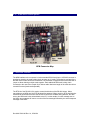
Single Channel Network Power
Margin Card User Manual
Doc # 98-37821-00 Rev 1.4, 07/20/04
1.0 Product Description .......................................................................................................... 3
1.1 NPM Feature Summary ........................................................................................................................... 3
1.2 Product Specifications ............................................................................................................................. 4
2.0 Interface Description ....................................................................................................... 6
2.1 Electrical Interface.................................................................................................................................... 6
2.2 Margin Card Connector Pinouts and Jumpers ......................................................................................... 8
2.2.1 RS-485 Connector J1............................................................................................................................ 8
2.2.2 LED Connector J2 ................................................................................................................................ 8
2.2.3 Reset Connector J4 ............................................................................................................................... 8
2.2.4 Power Input Connector J5 .................................................................................................................... 8
2.2.5 Margined Power Output Connector J7 ................................................................................................. 9
2.2.6 RS-232 Connector J8............................................................................................................................ 9
2.2.7 Fixed Power Output Connector J9........................................................................................................ 9
2.2.8 Tri-state Control Connector J10 ......................................................................................................... 10
2.2.9 Network Address Jumpers JP1 ........................................................................................................... 10
3.0 Software Interface ............................................................................................................. 11
3.1 Addressing............................................................................................................................................. 11
3.2 Command Descriptions ......................................................................................................................... 12
3.2.1 DIAG Command (0x01)..................................................................................................................... 12
3.2.2 LED Command (0x02) ....................................................................................................................... 12
3.2.3 Set Voltage Command (0x03) ............................................................................................................ 13
3.2.4 Set Slew Rate Command (0x04)......................................................................................................... 13
3.2.5 Get Status Command (0x05) .............................................................................................................. 14
3.2.6 Get Profile Data Command (0x06).................................................................................................... 14
3.2.7 Soft Reset Command (0x07) .............................................................................................................. 15
3.2.8 Set Com Port Command (0x08) ......................................................................................................... 15
3.2.9 Start Profile Command (0x09) ........................................................................................................... 16
4.0 Miscellaneous Hardware Properties ................................................................ 17
4.1 Linearity ................................................................................................................................................ 17
4.2 High Current Loads ............................................................................................................................... 17
Doc # 98-37821-00 Rev 1.4, 07/20/04
1.0 Product Description
The Flexstar Single Channel Network Power Margin card (NPM) P/N 02-37351-00 consists of
four compact switching DC-to-DC converters designed to provide two ‘programmable’ voltage
outputs and two ‘fixed’ voltage outputs. The first programmable channel (5V nominal) can be
programmed from 0 to 7.5V while the second programmable channel (12V nominal) can be
programmed from 0 to 15V. Slew rates can be controlled in 1-millisecond increments for
applications requiring moderate rise and fall times. The fixed outputs are +5V at 8A and +12V at
1A, which is sufficient to power most SBC’s (single board computers). The input voltage can be
from 15 to 24VDC.
Up to 16 NPM cards can be daisy chained together via an on-board RS-485 party line network.
The NPM card has its own Micro-controller that handles the communication, addressing, and
internal voltage algorithms and calibration. A 4-position jumper header on each card determines
the unique network address for each card.
Each NPM card has provisions for up to 3 LED’s, which can be turned on, off, or blinked at a
programmable rate.
Voltage and current measurement is built into the design and can measure peak load currents on
both margin channels up to 5 Amperes. In addition, the NPM card has on-board memory for
acquiring power samples with programmable sample rates. This provides a ‘snapshot’ mode for
capturing power profiles.
The NPM cards are designed to operate stand-alone or be cabled together to provide multiple
channels of power with a single RS232 connection to a PC. The NPM is a 4.5”W x 3.5D” x 1.75”H
circuit board that contains all circuitry for the two margined and two fixed channels.
Additionally a 3-pin header (J10) provides an interface to the Flexstar IDE UDMA-100 card in
order to control the tri-state circuitry on the IDE card. Also, a 2-pin header labeled ‘RESET’ is
provided to connect the reset button to a SBC so that this switch functions as the master reset
switch for all hardware. When ‘RESET’ is asserted, this will force the programmable channels to
return to zero volts and the LED’s to turn off.
1.1 NPM Feature Summary
¾
¾
¾
¾
¾
¾
¾
¾
¾
¾
Two independently programmable voltage outputs.
Two fixed voltage outputs for powering a SBC, etc.
RS-485 network allows up to 16 NPM’s to be connected to a single PC.
Simple serial interface protocol.
Built-in Micro-Controller provides communications and low-level control.
High accuracy and resolution.
Voltage and current measurement capability.
On-board memory for power sampling data acquisition.
Built-in RS-232 to RS-485 converter.
Broadcast mode for parallel device operation.
Doc # 98-37821-00 Rev 1.4, 07/20/04
1.2 Product Specifications
See also section 4.0 for more details on specifications.
General
Input Voltage Range:
Max Input Current:
Regulator efficiency:
15V to 24V DC.
6.7 Amps (input = 15V, output = 100W).
Approximately 94%.
NPM Voltage Channel #1
Range:
Accuracy Typical:
Accuracy Maximum:
Peak Power:
Max Current:
0 volts to 7.5 volts in 2.4 millivolt increments. See also section 4.1.
+/- 0.5% typical (Note 1).
+/- 1% of set voltage (Note 1).
6 Amps for 10 seconds.
3.5 Amps (continuous). See also section 4.2.
NPM Voltage Channel #2
Range:
Accuracy Typical:
Accuracy Maximum:
Peak Power:
Max Current:
0 volts to 15 volts in 5.8 millivolt increments. See also section 4.1.
+/- 0.5% typical (Note 1).
+/- 1% of set voltage (Note 1).
6 Amps for 10 seconds.
3.5 Amps (continuous). See also section 4.2.
Fixed Voltage Power Outputs
5V Max Current:
5V Peak Power:
12V Channel:
12V Peak Power:
8 Amps (continuous). See also section 4.2.
10 Amps for 5 seconds.
1 Amp (continuous).
1.5 Amps for 10 seconds.
NPM Current Measurement (both margin channels)
Range:
Resolution:
Accuracy:
0 to 5 Amps.
1.22 milliamps.
+/- 1% of full scale.
NPM Voltage Measurement (Read-back)
Range:
Resolution:
Accuracy:
0 to 7.5V (Ch0) 0 to 15V (Ch1)
2 mV (Ch0) 4 mV (Ch1)
+/- 1.5% of full scale
Margin Card Power Sampling (both margin channels)
Samples:
Sample Rate:
2048 for each channel.
1 to 255 milliseconds in 1 milliseconds increments.
NPM Physical Dimensions
Length:
Width:
4.5 inches (11.4 cm)
3.5 inches (8.9 cm)
Doc # 98-37821-00 Rev 1.4, 07/20/04
Height:
1.75 inches (4.4 cm)
Airflow, Linear Feet Per Minute
LFM:
100
Notes:
1) Test conditions: Channel tested with a 1 amp static (resistive) load. Maximum cable
length = 1 meter (39 inches) 20 gauge wire. Voltage measured at the load.
Doc # 98-37821-00 Rev 1.4, 07/20/04
2.0 Interface Description
NPM Connector Map
2.1 Electrical Interface
The NPM interface to the computer is via the standard RS-232 serial port. A RS-485 converter is
supplied on-board to be used to daisy chain as many as 16 cards. The beginning and end of the
RS-485 network cable should be terminated. This terminator is supplied on the each NPM with a
jumper to allow chaining multiple cards together. Each additional NPM card is daisy chain
connected to the next with a simple 10-pin ribbon cable. Maximum length of the cable should not
exceed 25 meters (baud rate dependant).
The RTS bit of the RS-232 I/O is used to control the direction of the RS-485 drivers. When
transmitting to an NPM card, the RTS bit should be asserted. When receiving, RTS should be deasserted. Be aware also that since the RS-232 receivers are enabled during transmit, the data
sent to the NPM card is also echoed back to the PC. In other words, for each message sent to
the NPM, two messages will return: an echo of the first message followed by the actual response
message of the NPM.
Doc # 98-37821-00 Rev 1.4, 07/20/04
Note in the figure above that the RS-485 terminator jumper should always be installed on the first
and last cards in the daisy chain. All other cards in the daisy chain should have the terminator
jumper removed. For a single card installation, the terminator jumper should be installed.
Doc # 98-37821-00 Rev 1.4, 07/20/04
2.2 Margin Card Connector Pinouts and Jumpers
2.2.1 RS-485 Connector J1
J1 is a 10-pin male header connector designed to connect to a 10-pin female ribbon cable
connector.
Pin
1
2
3
4
5
6
7
8
9
10
Description
GROUND
- RS-485
GROUND
GROUND
GROUND
GROUND
GROUND
GROUND
+ RS-485
GROUND
2.2.2 LED Connector J2
Pin
1
2
3
4
5
6
7
8
9
10
Description
+5V (Red LED Anode)
Red LED Cathode
+5V (Green LED Anode)
Green LED Cathode
+5V (Yellow LED Anode)
Yellow LED Cathode
Nc
Nc
Nc
Nc
2.2.3 Reset Connector J4
The J4 connector is a two-pin header connector, which provides an external reset for an attached
SBC or other device. A 2-pin cable is normally attached between J4 and the SBC reset
connector. Note that the polarity of the J4 connector must match the polarity of the reset input on
the SBC. If incorrect, the SBC will remain reset indefinitely.
Pin
1
2
Description
Ground
N.O. pushbutton switch contact with a 20K pull-up to +5V.
2.2.4 Power Input Connector J5
Doc # 98-37821-00 Rev 1.4, 07/20/04
J5 is a 4 pin 0.156” spacing Molex type connector and is the main DC power input connector for
the NPM.
Pin
1
2
3
4
Description
+15V to +24V In
+15V to +24V In
GROUND
GROUND
2.2.5 Margined Power Output Connector J7
J7 is a 10-pin boxed male header connector and is the output connector for both programmable
voltage channels.
Pin
1
2
3
4
5
6
7
8
9
10
Description
+12V
+12V
+12V Sense
GROUND
GROUND Sense
GROUND
GROUND
+5V Sense
+5V
+5V
2.2.6 RS-232 Connector J8
J8 is a 10-pin male header that provides the main RS-232 control input to the NPM card.
Pin
1
2
3
4
5
6
7
8
9
10
Description
N/C
N/C
RS232 receive input.
RTS – used to steer the RS-485 direction.
RS232 transmit output
N/C
N/C
N/C
GROUND
N/C
2.2.7 Fixed Power Output Connector J9
J9 is a 10-pin boxed male header connector and is the output connector for both fixed voltage
channels.
Pin
1
2
Description
+12V
+12V
Doc # 98-37821-00 Rev 1.4, 07/20/04
3
4
5
6
7
8
9
10
+12V
GROUND
GROUND
GROUND
GROUND
+5V
+5V
+5V
2.2.8 Tri-state Control Connector J10
J10 is a three pin SIP header connector that is intended to provide a low/high signal to an
external HBA card containing tri-stating circuitry. The middle pin of this connector is connected to
the programmable 5V channel such that when 5V is applied to the external device, the tri-state
circuit is on (LOWZ state). When the 5V channel is at zero volts, the tri-state circuit will be off
(HIGHZ state).
Pin
1
2
3
Description
GROUND
5V programmable output channel. 1=LOWZ, 0=HIGHZ.
GROUND
2.2.9 Network Address Jumpers JP1
JP1 is a 8 pin header used to provide jumpering options for the network address. The jumpers
are numbered 0 to 3 and can be arranged as follows:
JP0
In
Out
In
Out
In
Out
In
Out
In
Out
In
Out
In
Out
In
Out
JP1
In
In
Out
Out
In
In
Out
Out
In
In
Out
Out
In
In
Out
Out
JP2
In
In
In
In
Out
Out
Out
Out
In
In
In
In
Out
Out
Out
Out
Doc # 98-37821-00 Rev 1.4, 07/20/04
JP3
In
In
In
In
In
In
In
In
Out
Out
Out
Out
Out
Out
Out
Out
Address
0 - default
1
2
3
4
5
6
7
8
9
10
11
12
13
14
15
3.0 Software Interface
Communication is accomplished from a Serial Com port of the PC to an NPM by sending a
simple serial command packet. The command packet contains a unique identifier along with an
address, command, command arguments, and a checksum. The checksum is a simple one-byte
value, which is produced by adding all bytes in the packet and masking the byte remainder of the
summation.
A command packet is as follows:
STX AAh 55h ADR CMD ARG1 ARG2 ARG3 ARG4 SUM
Where STX = Start of text char (FEh)
AAh = unique msg ID (constant)
55h = unique msg ID (constant)
ADR = target address (0 – 127)
CMD = command byte
ARG1 = 1st arg byte
ARG2 = 2nd arg byte
ARG3 = 3rd arg byte
ARG4 = 4th arg byte
SUM = checksum of data from STX thru ARG4
Checksum example:
FE AA 55 00 01 00 00 00 02
The NPM will respond with a packet similar to the command packet:
ETX 55h AAh ADR STAT LEN1 LEN2 -DATA- SUM
Where ETX = End of text char (FDh)
55h = unique msg ID (constant)
AAh = unique msg ID (constant)
ADR = address of the target
STAT = low nibble: last command, high nibble: status * NOTE 1
LEN1 = Low byte of length word (header + data + checksum)
LEN2 = High byte of length word
-DATA- = data if LEN > 8 (8 is the base header size including checksum)
SUM = checksum of data from ETX to end of -DATA-.
Checksum example:
FD 55 AA 00 11 08 00 00 1B
|
Æ Status Byte
NOTE 1: The possible status values returned in the upper nibble are:
ACK – 0x10
PROFILE_RDY – 0x20
The lower nibble of the status byte will always contain the last sent command byte.
Most commands will respond immediately. The exceptions to this are the SET_COM_PORT and
the SOFT_RESET command, which do not respond at all.
3.1 Addressing
Doc # 98-37821-00 Rev 1.4, 07/20/04
Each device present on the network will respond to it’s own unique address determined by the
jumper setting on JP1. In addition, all devices will respond to the BROADCAST address 0xFF.
NOTE: Broadcast functions will NOT generate a response to the Host since this would result in a
network conflict with two or more devices attempting to utilize the network simultaneously.
3.2 Command Descriptions
3.2.1 DIAG Command (0x01)
The diagnostic command provides a method for establishing communication with an NPM card.
This command’s expected response should be an ACKNOWLEDGE packet indicating successful
communications.
Command Packet:
FE AA 55 adr 01 00 00 00 00 sum
Where adr = target address (0 – 127)
sum = checksum
Expected Response:
FD 55 AA adr 11 08 00 sum
|
Æ Status Byte
3.2.2 LED Command (0x02)
The LED command provides the method for controlling the ON/OFF, and BLINK state of the three
LED’s. The default blink rate is fixed at 250-millisecond ON/OFF time. The blink rate can be
changed using a non-zero value in BR. Each increment of BR is equal to a 25 ms ON/OFF time.
In addition, two mode bits are present to allow the YELLOW LED to operate in different modes
(see table below).
All LED’s are set OFF after power on or reset.
Command Packet:
Where adr =
led =
FE AA 55 adr 02 led BR 00 00 sum
target address (0 – 127)
bit 0 - RED LED ON
bit 1 - GREEN LED ON
bit 2 – YELLOW LED ON
bit 3 – YELLOW LED Mode bit 0 (see below)
bit 4 – Blink RED LED
bit 5 – Blink GREEN LED
bit 6 – Blink YELLOW LED
bit 7 – YELLOW LED Mode bit 1 (see below)
BR=
Blink rate in 25 ms increments. Value of zero uses the default 250 ms.
sum = checksum
Expected Response:
FD 55 AA adr 12 08 00 sum
Yellow LED Usage
Normal – Same as Red & Green Led’s
External Signal Indicator (0 = ON, 1 = OFF)
Doc # 98-37821-00 Rev 1.4, 07/20/04
Mode bit 0
0
1
Mode bit 1
0
0
Power On Indicator (ON when 5V > 0)
0
1
3.2.3 Set Voltage Command (0x03)
The set voltage command will set the output voltage for both channels using the SLEW RATE set
by the SET SLEW RATE command. Values for each channel are in millivolts. Example: 5.25 V =
5250 millivolts. Default after power up is ZERO volts for both channels.
Note that the upper two bits of the 5V value are used as control options – see note below.
Command Packet:
Where adr =
5L =
5H =
12L =
12H =
sum =
FE AA 55 adr 03 5L 5H 12L 12H sum
target address (0 – 127)
low byte of the 5 volt value (in millivolts).
high byte of the 5 volt value (in millivolts).
low byte of the 12 volt value (in millivolts).
high byte of the 12 volt value (in millivolts).
checksum
Expected Response:
FD 55 AA adr 13 08 00 sum
Note: The upper two bits of the 5H byte are used as power control options as follows:
Bit 7: If = 1, sets the voltage values but does not cause the voltage to change. This is used to
set voltage prior to using the START PROFILE command with the option to start power
synchronous with sampling.
Bit 6:
Reserved.
3.2.4 Set Slew Rate Command (0x04)
Using this command controls the slew rate for each channel. The default slew rate is 10
milliseconds. Each channel can be programmed from 0 to 255 milliseconds. Micro-stepping the
voltage from the current set point to the new set point creates a slew. Note that even though slew
rate arguments accept a 16 bit value, only the low 8 bits are considered.
Command Packet:
Where adr =
1L =
1H =
2L =
2H =
sum =
FE AA 55 adr 04 1L 1H 2L 2H sum
target address (0 – 127)
low byte of the 5 volt channel slew rate.
high byte of the 5 volt channel slew rate.
low byte of the 12 volt channel slew rate.
high byte of the 12 volt channel slew rate.
checksum
Expected Response:
FD 55 AA adr 14 08 00 sum
Doc # 98-37821-00 Rev 1.4, 07/20/04
3.2.5 Get Status Command (0x05)
The GET_STATUS command provides a method for the Host PC to acquire feedback from the
NPM. The feedback provides voltage and current for each channel, temperature, and a firmware
version number.
Command Packet:
FE AA 55 adr 05 00 00 00 00 sum
Where adr = target address (0 – 127)
sum = checksum
Expected Response:
FD 55 AA adr 15 SL SH V5L V5H I5L I5H V12L V12H I12L I12H TPL
TPH VER sum
Where adr = target address (0 – 127)
SL = Status Low Byte (* see “Status Byte” below)
SH = Status High Byte
V5L = low byte of the 5 volt channel voltage (in MV). * NOTE 2
V5H = high byte of the 5 volt channel voltage.
I5L = low byte of the 5 volt channel current (in MA).
I5H = high byte of the 5 volt channel current.
V12L = low byte of the 12 volt channel voltage (in MV).
V12H = high byte of the 12 volt channel voltage.
I12L = low byte of the 12 volt channel current (in MA).
I12H = high byte of the 12 volt channel current.
TPL = Temperature low byte (in 0.1 deg incrs).
TPH = Temperature high byte (MSB set if negative temp).
VER = Hex based version number – example: 0x10 = version 1.0
sum = checksum
Status Byte:
7
6
5
4
3
2
1
0
|
|
|
|
|
----------- ACK
|
---------------------- Profile Ready
--------------------------------- External Input Active
NOTE 2: The values received are RAW A/D values. The values should be multiplied by 1.222 to
obtain the correct value. 1.222 is the ratio between the 12-bit ADC resolution (4096) and the 5volt reference voltage.
3.2.6 Get Profile Data Command (0x06)
The GET PROFILE DATA command is used to upload the sampled data from the NPM buffer
(see also START PROFILE command). When the command is received, the NPM will begin
sending the number of samples specified to the Host. This operation takes a maximum of 850
milliseconds at 115.2K baud.
Note also that the command accepts an offset value. The offset is NOT the actual buffer offset
but rather a sample offset. For example, to upload 200 samples starting at sample 1000, LL,LH
would be = 200, and OL,OH would be = 1000. This feature can be used to break large sample
uploads into smaller packets or can be used to ‘zoom’ into smaller segments of the buffer.
Command Packet:
Where adr =
LL =
FE AA 55 adr 06 LL LH OL OH sum
target address (0 – 127)
number of samples to return low byte.
Doc # 98-37821-00 Rev 1.4, 07/20/04
LH =
OL =
OH =
sum =
Expected Response:
Where adr =
DATA
sum =
number of samples to return high byte. (Max = 2048).
offset low byte.
offset high byte.
checksum
FD 55 AA adr 36 08 20 DATA sum
target address (0 – 127)
Number of bytes = samples x 4. * NOTE 3
checksum
NOTE 3: Data is organized as follows:
Byte 0 - low byte of 5V current
Byte 1 - high byte of 5V current.
Byte 2 - low byte of 12V current.
Byte 3 high byte of 12V current.
… repeated ‘n’ times
See also NOTE 2.
3.2.7 Soft Reset Command (0x07)
A soft reset is provided to effectively perform the same operation as a power on or hard reset.
Both channels will be forced to zero volts and the circuitry will be re-calibrated. This command will
not produce a response to the Host PC.
Command Packet:
FE AA 55 adr 07 00 00 00 00 sum
Where adr = target address (0 – 127)
sum = checksum
Expected Response:
NONE
3.2.8 Set Com Port Command (0x08)
This command sets the baud rate for the NPM’s serial port. The NPM will initially connect at
19.2K baud but other baud rates (up to 115.2K) may be selected depending on the environment
and the length of the RS-485 cable. No response will be generated by this command. Verification
of communication at the new baud rate can be done using the DIAG or GET STATUS
commands. Default setting on power up or reset are:
Baud rate: 19.2K baud (see also NOTE 4).
Parity:
None.
Stop bits: 1.
Command Packet:
Where adr =
BR =
sum =
FE AA 55 adr 08 BR 00 00 00 sum
target address (0 – 127)
Baud rate code * NOTE 4
checksum
Expected Response:
NONE
NOTE 4: The baud rate codes are as follows:
1=
115.2 K Baud
2=
57.6 K Baud
Doc # 98-37821-00 Rev 1.4, 07/20/04
3=
4=
5=
38.4 K Baud
19.2 K Baud
9600 Baud
Selecting the highest baud rate possible will dramatically improve system performance when
using the GET PROFILE command.
3.2.9 Start Profile Command (0x09)
The START PROFILE command is used to initiate a sampling of the power consumption on both
power channels. When the command is received, the NPM will then begin sampling at the
desired sample rate until the sample buffer is full. The sample buffer holds a maximum of 2048
samples for each channel. If a one millisecond sample rate is commanded, the buffer will be full
about 2 seconds after the command is received (2048 x 1 ms). Use the GET PROFILE DATA
command to retrieve the data.
After this command is received, the NPM will issue an ACKNOWLEDGE response and then
begin sampling. When the command is finished, the STATUS byte returned from the GET
STATUS command will contain a flag (bit 5) that indicates the profile buffer has been loaded and
may be retrieved using the GET PROFILE DATA command.
If a GET STATUS command is received during sampling, the command is ignored. If any other
command is received during sampling, sampling is aborted and that command is executed. This
allows sampling to be aborted at any time.
Note that the upper four bits of the ‘samples’ word (LH, LL) are used as control options. See note
below.
Command Packet:
Where adr =
SL =
SH =
LL =
LH =
sum =
FE AA 55 adr 09 SL SH LL LH sum
target address (0 – 127)
low byte of the sample rate (in milliseconds).
high byte of the sample rate (in milliseconds).
number of samples low byte.
number of samples high byte. (Max samples = 2048).
checksum
Expected Response:
FD 55 AA adr 19 08 00 sum
Where adr = target address (0 – 127)
sum = checksum
Note: The upper four bits of the samples word (high nibble of LH) are used as control options as
follows:
Bit 7: Enable power prior to sampling. This requires a SET VOLTAGE command to be sent
prior to this command with bit 7 of the ‘samples’ word set = 1 (see SET VOLTAGE command).
Bit 6,5,4: Reserved.
Doc # 98-37821-00 Rev 1.4, 07/20/04
4.0 Miscellaneous Hardware Properties
Please take note of the properties of this design to utilize the product correctly.
4.1 Linearity
The output voltage is not linear over the entire programming range. The following table shows the
results of various set points versus actual output:
5V Channel Set point
>= 1.6V
1.5V
< 1.4V
Actual
Linear Range
1.4V
Approx. 0V
12V Channel Set Point
>= 3.2V
3V
< 2.8V
Actual
Linear Range
2.8V
Approx. 0V
Typical Linear Region of +5V Channel
8.000
7.000
6.000
5.000
4.000
3.000
2.000
1.000
0.000
1.0 1.2 1.4 1.6 1.8 2.0 2.2 2.4 2.6 2.8 3.0 3.2 3.4 3.6 3.8 4.0 4.2 4.4 4.6 4.8 5.0 5.2 5.4 5.6 5.8 6.0 6.2 6.4 6.6 6.8 7.0 7.2 7.4
00 00 00 00 00 00 00 00 00 00 00 00 00 00 00 00 00 00 00 00 00 00 00 00 00 00 00 00 00 00 00 00 00
-1.000
Expected Voltage Settings (Volts)
4.2 High Current Loads
Under high current loads, the NPM will require some amount of airflow to prevent overheating of
the regulator FET’s. The following table shows approximate airflow versus output power:
Total Output (Watts)
0 to 20
Doc # 98-37821-00 Rev 1.4, 07/20/04
Air Volume
0
20 to 50
50 to 100
Doc # 98-37821-00 Rev 1.4, 07/20/04
35 cfm
100 cfm
Command Descriptions
DIAG Command (0x01)........................................................................................................................... 11
Get Profile Data Command (0x06)........................................................................................................... 13
Get Status (0x05)...................................................................................................................................... 13
LED Command (0x02) ............................................................................................................................. 11
Set Com Port Command (0x08) ............................................................................................................... 14
Set Slew Rate Command (0x04) .............................................................................................................. 12
Set Voltage Command (0x03) .................................................................................................................. 12
Soft Reset Command (0x07) .................................................................................................................... 14
Start Profile Command (0x09) ................................................................................................................. 15
Connector Pinouts and Jumpers
RS-485 Connector J1.................................................................................................................................. 7
Connectors Pinouts and Jumpers
Fixed Power Output Connector J9.............................................................................................................. 8
LED Connector J2 ...................................................................................................................................... 7
Margined Power Output Connector J7 ....................................................................................................... 8
Network Address Jumpers JP1 ................................................................................................................... 9
Power Input Connector J5 .......................................................................................................................... 7
Reset Connector J4 ..................................................................................................................................... 7
RS-232 Connector J8.................................................................................................................................. 8
Tri-state Control Connector J10 ................................................................................................................. 9
Interface Description ...................................................................................................................................... 5
Connector Pinouts and Jumpers ................................................................................................................. 7
Electrical Interface...................................................................................................................................... 5
Miscellaneous Hardware Properties ............................................................................................................. 16
High Current Loads .................................................................................................................................. 16
Linearity ................................................................................................................................................... 16
Product Description .................................................................................................................................... 3, 4
Feature Summary ....................................................................................................................................... 3
Specifications ............................................................................................................................................. 4
Software Interface ........................................................................................................................................ 10
Addressing................................................................................................................................................ 10
Command Descriptions ............................................................................................................................ 11
Doc # 98-37821-00 Rev 1.4, 07/20/04