1
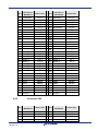
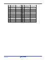
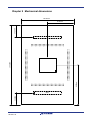
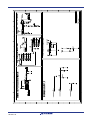
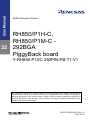
User Manual RH850 Evaluation Platform RH850/P1H-C, RH850/P1M-C 32 292BGA PiggyBack board Y-RH850-P1XC-292PIN-PB-T1-V1 All information contained in these materials, including products and product specifications, represents information on the product at the time of publication and is subject to change by Renesas Electronics Corp. without notice. Please review the latest information published by Renesas Electronics Corp. through various means, including the Renesas Technology Corp. website (http://www.renesas.com). www.renesas.com R20UT3314ED0100, Rev. 1.0 2015-01-19 Table of Contents Chapter 1 Introduction ......................................................................... 3 Chapter 2 Overview .............................................................................. 4 2.1 2.2 Overview ............................................................................................... 4 Mounting of the device ........................................................................ 5 Chapter 3 Power supply ....................................................................... 6 3.1 3.2 Board power connection ..................................................................... 6 Voltage distribution .............................................................................. 7 Chapter 4 Clock sources ...................................................................... 9 4.1.1 4.1.2 MainOsc .........................................................................................................................9 Programmable Oscillator .............................................................................................9 Chapter 5 Debug and Programming interface .................................. 10 Chapter 6 Connectors for ports of device......................................... 11 6.1 6.2 6.3 6.4 Connectors for ADC voltage supply ................................................. 11 Push button for RESET ...................................................................... 11 Mode Selection ................................................................................... 11 Connectors to MainBoard .................................................................. 12 6.4.1 6.4.2 Connector CN1 ............................................................................................................12 Connector CN1 ............................................................................................................13 Chapter 7 Other circuitry.................................................................... 16 7.1 7.2 Signalling for CVMOUTZ and ERROROUTZ ..................................... 16 Pin Headers for Pull-Down and Pull-Up............................................ 16 Chapter 8 Precautions ........................................................................ 17 8.1 Missing Connection to CN1 ..................... Error! Bookmark not defined. Chapter 9 Mechanical dimensions .................................................... 18 Chapter 10 Schematic .......................................................................... 19 Chapter 11 Revision History ................................................................ 23 R20UT3314ED0100 Rev. 1.0 2015-01-19 2 Chapter 1 Introduction The RH850/P1H-C and RH850/P1M-C Application Board is part of the RH850 Evaluation Platform and serves as a simple and easy to use platform for evaluating the features and performance of Renesas Electronics 32-bit RH850/P1H-C and RH850/P1M-C microcontrollers in a BGA292 package. The PiggyBack board (Y-RH850-P1XC-292PIN-PB-T1-V1) can be used as a standalone board, or can be mated with a mainboard (e.g. Y-RH850-X1X-MB-T1V1) for extended functionality. Main features: Socket for mounting of device Standalone operation of the board Direct supply of device voltage (typ. 3.3V and 1.25V) enabling single power supply and dual power supply Device programming capability Device debugging capability Pin headers for direct access to each functional device pin Reset switch MainOSC circuitry Connectors to MainBoard Operating temperature from 0°C to +40°C This document describes the functionality provided by the PiggyBack board and guides the user through its operation. For details regarding the operation of the microcontroller, refer to the corresponding User’s Manual. R20UT3314ED0100 Rev. 1.0 2015-01-19 3 Chapter 2 Overview 2.1 Overview Figures 1 and 2 provide a schematic view of the PiggyBack board. Figure 1 PiggyBack Board Schematic Top View The black arrow denotes the position of socket pin #1. Figure 2 PiggyBack Board Schematic Bottom View R20UT3314ED0100 Rev. 1.0 2015-01-19 4 2.2 Mounting of the device The board is designed for use with the following devices: RH850/P1H-C in BGA292 package and RH850/P1M-C in BGA292 package The device must be placed inside the socket IC1. To insert the device align the corner of the device package marked with a white triangle (see picture below) with the #1pin of the socket. The #1pin of the socket is marked with a circle near to the “IC1” label (see also black arrow in Figure 1). Figure 3 Alignment Mark on Device Package First insert the device into the socket with closed mount. Then press down the lid of the socket until the device slips into the socket and finally release the lid. CAUTION: Please follow the mounting instruction carefully as described. Otherwise the device might get damaged. R20UT3314ED0100 Rev. 1.0 2015-01-19 5 Chapter 3 Power supply 3.1 Board power connection For operation of the device, a supply voltage must be connected to the board. There are several possibilities to power the device. Within this document the following voltages are considered as ‘typical’ connections: Voltage1 = 3.3V Voltage2 = 1.25V Direct voltage supply Two different voltages can be supplied to the board. The following connectors are available to supply those voltages directly: Three 4mm ‘banana-type’ connectors: - Two red connectors for voltages Voltage1 (CN23) and Voltage2 (CN24). - A black connector for ground (GND) connection (CN22). Note: The three connectors are supplied with the board but not assembled. For details about voltage distribution, refer to Chapter 3.2 ‘Voltage distribution’. Supply by MainBoard In case the PiggyBack board is mounted on a MainBoard, the voltage Voltage1 is supplied by the on-board regulator of the MainBoard. CAUTION: Do not supply Voltage1 directly to the PiggyBack board in case it is mounted on the MainBoard. For each of the voltages, Voltage1 and Voltage2 a green LED is available to signal that the related voltage is available on the PiggyBack board. The corresponding LEDs are placed directly beneath the connectors of the related voltage. R20UT3314ED0100 Rev. 1.0 2015-01-19 6 3.2 Voltage distribution The table shows the required device power supply pins and their function. For detailed explanation of their function, please refer to the user documentation of the corresponding device: Device Supply Pin SYSVCC VCC EnVCC (n = 0, 1) AnVCC (n = 0, 1) AnVREFH (n = 0, 1) VDD (VCL) Additional one power supply for the MainBoard can be selected: Supply voltage Function IO supply voltage for components located on a connected mainboard. VDDIOF The following figure shows the configurable voltage distribution on the PiggyBack board. Voltage1 JP1 JP0 JP6 JP2 SYSVCC JP3 VCC JP4 E0VCC JP5 E1VCC JP7 A0VCC JP8 A0VREFH JP9 A1VCC JP10 A1VREFH VDDIOF Voltage1 Voltage2 Voltage regulator for VDD JP11 JP12 VCL/VDD Figure 4 Voltage Distribution on the PiggyBack Board All power supply lines can be interrupted by jumpers. This provides the possibility to measure the current consumption of each individual power domain of the device (JP2 – 5, JP7 – 10 and JP12). The IO supply voltage for the Mainboard (VDDIOF) can be connected via jumper JP1 to Voltage1, if the PiggyBack board is mounted on a MainBoard. In case of a DPS device, VDD can be powered either directly from the ‘banana-type’ connector (Voltage2 – CN24) or by an on-board voltage regulator. Thereby even a DPS device can be operated with one single voltage supply (Voltage1). The source for VDD is selectable by the jumper JP11. The jumper JP12 connects the voltage, configured by JP11 with the VDD pins. R20UT3314ED0100 Rev. 1.0 2015-01-19 7 CAUTION: Jumper JP12 must not be connected in case of an eVR device. In this case the connected pins function as VCL pins and must not be supplied with a voltage. R20UT3314ED0100 Rev. 1.0 2015-01-19 8 Chapter 4 Clock sources One external crystal oscillator for the device clock supply is provided with the board. 4.1.1 MainOsc A crystal or ceramic resonator can be mounted on socket X1. A 16Mhz oscillator is supplied with the board. 4.1.2 Programmable Oscillator It is possible to mount a programmable crystal oscillator on the PiggyBack board at OSC1. The available footprint and circuitry is designed for a SG-8002CE programmable crystal oscillator from Epson Toyocom. The output from this oscillator can be connected to port X1 of the device via jumper JP13. The SG8002CE is neither mounted nor provided with the board. For details about the available circuitry refer to Chapter 10 ‘Schematic’. A resonator mounted on socket X1 must not be used in parallel to another clock source. R20UT3314ED0100 Rev. 1.0 2015-01-19 9 Chapter 5 Debug and Programming interface For connection of the microcontroller debug and flash programming tools, the connector CN25 with fourteen pins is provided. The signal connection of the connector CN25 is shown in the table below: CN25 Pin Device Port Device Signal 1 JP0_2 TCK / LPDCLK / FLSCI3SCKI 2 GND GND 3 JP0_4 TRSTZ 4 FLMD0 FLMD0 5 JP0_1 TDO / LPDO / FLSCI3TXD 6 - - 7 JP0_0 TDI / LPDI / FLSCI3RXD / FLSCI3TXD 8 ‘Dbg_Voltage’ Voltage1 9 JP0_3 TMS 10 - - 11 JP0_5 RDYZ / LPDCLKOUT 12 GND - 13 RESET RESETZ 14 GND - R20UT3314ED0100 Rev. 1.0 2015-01-19 10 Chapter 6 Connectors for ports of device Connection to each functional pin of the devices is possible via the connectors CN5 to CN8. Some functions might not be available for every device. Therefore, please refer to the corresponding User’s Manual for available pins on the used device, and a detailed explanation of their function. CAUTION: The pin headers are directly connected to the pins of the device, therefore special care must be taken to avoid any electrostatic or other damage to the device. 6.1 Connectors for ADC voltage supply It is possible to apply the ADC related reference, as well as two input voltages via SMA connectors (CN10, CN11, CN13 and CN14). These are directly connected (JP8 and JP10 are bypassed) to the following pins of the device Device Port ADC0I0 A0VREFH ADC1I0 A1VREFH The SMA connectors are not mounted on nor provided with the boards. SMA connectors that fit to the following mounting holes available on the board can be mounted on the board 5.1mm 5.1mm Ø 1.6mm Figure 5 Mounting Holes for SMA Connectors 6.2 Push button for RESET In order to issue a RESET to the device, the push-button SW1 is available. 6.3 Mode Selection The PiggyBack Board gives the possibility to configure the following mode pins FLMD0 via jumper JP14 FLMD1 via jumper JP15 MODE0 via jumper JP16 MODE1 via jumper JP17 To apply “High” or “Low” to the mode pins, the pins 1 and 2, or the pins 2 and 3 of the corresponding jumper must be shorted, respectively. R20UT3314ED0100 Rev. 1.0 2015-01-19 11 Note: Pin 1 of the jumpers is marked by a small circle. CAUTION: Be careful in configuration of mode related pins, as wrong configuration can cause irregular behaviour of the devices. Be sure to check the corresponding User Manual, for details, which modes can be selected for the used device. 6.4 Connectors to MainBoard Two connectors (CN1 and CN2) are available to connect the PiggyBack board to a MainBoard. Regarding the function on the MainBoard, please refer to the UM of a supported MainBoard. Some functions might not be available for every device. Therefore, please refer to the corresponding User’s Manual for available pins on the used device, and a detailed explanation of their function. 6.4.1 Connector CN1 Pin Function on MainBoard Device Port Pin Function on MainBoard Device Port 1 - - 2 - - 3 - - 4 - - 5 RESET RESETZ 6 7 P5_7 - 8 9 INT0 P4_7 10 INT1 P4_12 11 INT2 P5_13 12 INT3 P0_5 - 14 13 - NMI - - - - - 15 UART0TX P5_14 16 UART1TX P5_5 17 UART0RX P5_13 18 UART1RX P5_4 19 LIN0TX P5_14 20 LIN1TX P5_5 21 LIN0RX P5_13 22 LIN1RX P5_4 23 - - 24 - - 25 - - 26 - - 27 CAN0TX P5_1 28 CAN1TX P5_9 29 CAN0RX P5_0 30 CAN1RX P5_10 31 SENT0IN P0_0 32 SENT1IN P0_1 33 SENT0OUT P2_4 34 SENT1OUT P3_9 35 - - 36 - - 37 - - 38 - - 39 - - 40 - - 41 FLX0TX P3_7 42 FLX0EN 43 FLX0RX P3_2 44 - 45 FLX1TX P7_3 46 FLX1EN 47 FLX1RX P7_2 48 - - - 50 - - 49 - P3_5 P7_1 51 ETH0MDIO P3_3 52 ETH0MDC P3_6 53 ETH0RXD0 P4_3 54 EH0TXD0 P3_9 55 ETH0RXD1 P4_4 56 EH0TXD1 P3_10 R20UT3314ED0100 Rev. 1.0 2015-01-19 12 Pin Function on MainBoard Device Port Pin Function on MainBoard Device Port 57 ETH0RXD2 P4_5 58 EH0TXD2 P3_12 59 ETH0RXD3 P4_6 60 EH0TXD3 P3_13 61 ETH0RXDCLK P4_2 62 ETH0TXCLK P4_1 63 ETH0RXER P4_0 64 ETH0TXER P3_8 65 ETH0CRSDV P3_7 66 ETH0TXEN P3_14 67 ETH0RXDV P4_7 68 ETH0COL P3_5 69 ETH0RESET P3_0 70 ETH0LINK P3_1 71 - - 72 - - 73 - - 74 - - 75 - - 76 - - 77 - - 78 - - 79 - - 80 - - 81 - - 82 - - 83 - - 84 - - 85 DIGIO_0 P6_0 86 DIGIO_1 P6_1 87 DIGIO_2 P6_2 88 DIGIO_3 P6_3 89 DIGIO_4 P6_4 90 DIGIO_5 P2_5 91 DIGIO_6 P2_6 92 DIGIO_7 P2_7 93 DIGIO_8 P2_8 94 DIGIO_9 P2_9 95 DIGIO_10 P2_10 96 DIGIO_11 P2_11 97 DIGIO_12 P2_12 98 DIGIO_13 P2_13 99 DIGIO_14 P2_14 100 DIGIO_15 P2_15 101 - 102 103 MUX0 P2_0 104 105 MUX2 P2_2 106 107 ADC0 ADC0I0 108 ADC1 ADC0I1 109 ADC2 ADC0I2 110 ADC3 ADC0I3 111 ADC4 ADC0I4 112 ADC5 ADC0I5 113 ADC6 ADC0I6 114 ADC7 ADC0I7 115 VDDIOF - 116 VDDIOF - 117 Voltage1 - 118 Voltage1 - 119 Voltage1 - 120 Voltage1 - 6.4.2 - MUX1 P2_1 - - Connector CN2 Pin Function on MainBoard Device Port Pin Function on MainBoard Device Port 1 CAN2TX P5_14 2 CAN3TX P9_7 3 CAN2RX P5_15 4 CAN3RX P9_8 5 - - 6 - - 7 - - 8 - - R20UT3314ED0100 Rev. 1.0 2015-01-19 13 Pin Function on MainBoard Device Port Pin Function on MainBoard Device Port 9 LIN2TX P7_5 20 LIN3TX P9_1 11 LIN2RX P7_4 22 LIN3RX P9_2 13 - - 14 - - 15 - - 16 - - 17 - - 18 - - 19 - - 20 - - 21 - - 22 - - 23 - - 24 - - 25 - - 26 - - 27 - - 28 - - 29 - - 30 - - 31 - - 32 - - 33 - - 34 - - 35 - - 36 - - 37 - - 38 - - 39 - - 40 - - 41 - - 42 - - 43 - - 44 - - 45 - - 46 - - 47 - - 48 - - 49 - - 50 - - 51 - - 52 - - 53 - - 54 - - 55 - - 56 - - 57 - - 58 - - 59 - - 60 - - 61 - - 62 - - 63 - - 64 - - 65 - - 66 - - 67 - - 68 - - 69 - - 70 - - 71 - - 72 - - 73 - - 74 - - 75 - - 76 - - 77 - - 78 - - 79 - - 80 - - 81 - - 82 - - 83 - - 84 - - 85 - - 86 - - 87 - - 88 - - 89 - - 90 - - 91 - - 92 - - 93 - - 94 - - R20UT3314ED0100 Rev. 1.0 2015-01-19 14 Pin Function on MainBoard Device Port Pin Function on MainBoard Device Port 95 - - 96 - - 97 - - 98 - - 99 - - 100 - - 101 - - 102 - - 103 - - 104 - - 105 - - 106 - - 107 - - 108 - - 109 - - 110 - - 111 - - 112 - - 113 - - 114 - - 115 - - 116 - - 117 - - 118 - - 119 - - 120 - - R20UT3314ED0100 Rev. 1.0 2015-01-19 15 Chapter 7 Other circuitry 7.1 Signalling for CVMOUTZ and ERROROUTZ Two red LEDs, LED1 and LED4 are available two indicate a “low” output signal from CVMOUTZ and ERROROUTZ, respectively. 7.2 Pin Headers for Pull-Down and Pull-Up A connector CN9 is available to enable easy connection to Voltage1 (3.3V) or GND via pull-up or pull-down resistances, respectively. Hereby uneven pins from 1 to 19 (in total ten) are configured as pull-up pin headers, while the even numbers from 2 to 20 (in total ten) can be used for pulldown. By connecting device port pins from CN5 – 8 to CN9 it is therefore possible to pull a desired port pin to “Low” or “High”. R20UT3314ED0100 Rev. 1.0 2015-01-19 16 Chapter 8 Precautions No limitations are known at the release of this document. R20UT3314ED0100 Rev. 1.0 2015-01-19 17 Chapter 9 Mechanical dimensions 100.00mm. 24,00mm 50.00mm. 80.00mm. 160,00mm CN2 24,00mm CN1 R20UT3314ED0100 Rev. 1.0 2015-01-19 18 Chapter 10 Schematic CAUTION: The schematic shown in this document is not intended to be used as a reference for mass production. Any usage in an application design is in sole responsibility of the customer. The following components described in the schematic are not provided with the board: SMA connectors o CN10 o CN11 o CN13 o CN14 Jumper JP13 Oscillator OSC1 Capacitors o C29 o C33 Resistances o R28 o R29 o R31 The following components described in the schematic are provided with but not mounted on the board: R20UT3314ED0100 Rev. 1.0 2015-01-19 Standard 4mm power lab sockets o CN22 o CN23 o CN24 19 R20UT3314ED0100 Rev. 1.0 2015-01-19 20 R20UT3314ED0100 Rev. 1.0 2015-01-19 21 R20UT3314ED0100 Rev. 1.0 2015-01-19 22 Chapter 11 Revision History The table provides information about the major changes of the document versions. Date Version 2015-01-19 1.0 R20UT3314ED0100 Rev. 1.0 2015-01-19 Description Initial release 23 Notice 1. All information included in this document is current as of the date this document is issued. Such information, however, is subject to change without any prior notice. Before purchasing or using any Renesas Electronics products listed herein, please confirm the latest product information with a Renesas Electronics sales office. Also, please pay regular and careful attention to additional and different information to be disclosed by Renesas Electronics such as that disclosed through our website. 2. Renesas Electronics does not assume any liability for infringement of patents, copyrights, or other intellectual property rights of third parties by or arising from the use of Renesas Electronics products or technical information described in this document. No license, express, implied or otherwise, is granted hereby under any patents, copyrights or other intellectual property rights of Renesas Electronics or others. 3. You should not alter, modify, copy, or otherwise misappropriate any Renesas Electronics product, whether in whole or in part. 4. Descriptions of circuits, software and other related information in this document are provided only to illustrate the operation of semiconductor products and application examples. You are fully responsible for the incorporation of these circuits, software, and information in the design of your equipment. Renesas Electronics assumes no responsibility for any losses incurred by you or third parties arising from the use of these circuits, software, or information. 5. When exporting the products or technology described in this document, you should comply with the applicable export control laws and regulations and follow the procedures required by such laws and regulations. You should not use Renesas Electronics products or the technology described in this document for any purpose relating to military applications or use by the military, including but not limited to the development of weapons of mass destruction. Renesas Electronics products and technology may not be used for or incorporated into any products or systems whose manufacture, use, or sale is prohibited under any applicable domestic or foreign laws or regulations. 6. Renesas Electronics has used reasonable care in preparing the information included in this document, but Renesas Electronics does not warrant that such information is error free. Renesas Electronics assumes no liability whatsoever for any damages incurred by you resulting from errors in or omissions from the information included herein. 7. Renesas Electronics products are classified according to the following three quality grades: "Standard", "High Quality", and "Specific". The recommended applications for each Renesas Electronics product depends on the product's quality grade, as indicated below. You must check the quality grade of each Renesas Electronics product before using it in a particular application. You may not use any Renesas Electronics product for any application categorized as "Specific" without the prior written consent of Renesas Electronics. Further, you may not use any Renesas Electronics product for any application for which it is not intended without the prior written consent of Renesas Electronics. Renesas Electronics shall not be in any way liable for any damages or losses incurred by you or third parties arising from the use of any Renesas Electronics product for an application categorized as "Specific" or for which the product is not intended where you have failed to obtain the prior written consent of Renesas Electronics. The quality grade of each Renesas Electronics product is "Standard" unless otherwise expressly specified in a Renesas Electronics data sheets or data books, etc. "Standard": Computers; office equipment; communications equipment; test and measurement equipment; audio and visual equipment; home electronic appliances; machine tools; personal electronic equipment; and industrial robots. "High Quality":Transportation equipment (automobiles, trains, ships, etc.); traffic control systems; anti-disaster systems; anti- crime systems; safety equipment; and medical equipment not specifically designed for life support. "Specific": Aircraft; aerospace equipment; submersible repeaters; nuclear reactor control systems; medical equipment or systems for life support (e.g. artificial life support devices or systems), surgical implantations, or healthcare intervention (e.g. excision, etc.), and any other applications or purposes that pose a direct threat to human life. 8. You should use the Renesas Electronics products described in this document within the range specified by Renesas Electronics, especially with respect to the maximum rating, operating supply voltage range, movement power voltage range, heat radiation characteristics, installation and other product characteristics. Renesas Electronics shall have no liability for malfunctions or damages arising out of the use of Renesas Electronics products beyond such specified ranges. R20UT3314ED0100 Rev. 1.0 2015-01-19 24 9. Although Renesas Electronics endeavors to improve the quality and reliability of its products, semiconductor products have specific characteristics such as the occurrence of failure at a certain rate and malfunctions under certain use conditions. Further, Renesas Electronics products are not subject to radiation resistance design. Please be sure to implement safety measures to guard them against the possibility of physical injury, and injury or damage caused by fire in the event of the failure of a Renesas Electronics product, such as safety design for hardware and software including but not limited to redundancy, fire control and malfunction prevention, appropriate treatment for aging degradation or any other appropriate measures. Because the evaluation of microcomputer software alone is very difficult, please evaluate the safety of the final products or system manufactured by you. 10. Please contact a Renesas Electronics sales office for details as to environmental matters such as the environmental compatibility of each Renesas Electronics product. Please use Renesas Electronics products in compliance with all applicable laws and regulations that regulate the inclusion or use of controlled substances, including without limitation, the EU RoHS Directive. Renesas Electronics assumes no liability for damages or losses occurring as a result of your noncompliance with applicable laws and regulations. 11. This document may not be reproduced or duplicated, in any form, in whole or in part, without prior written consent of Renesas Electronics. 12. Please contact a Renesas Electronics sales office if you have any questions regarding the information contained in this document or Renesas Electronics products, or if you have any other inquiries. (Note 1) "Renesas Electronics" as used in this document means Renesas Electronics Corporation and also includes its majority-owned subsidiaries. (Note 2) "Renesas Electronics product(s)" means any product developed or manufactured by or for Renesas Electronics. www.renesas.com R20UT3314ED0100 Rev. 1.0 2015-01-19 25