1
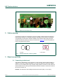
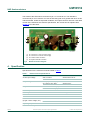
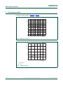
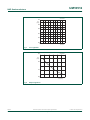
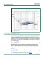
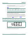
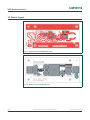
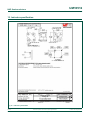
UM10512 SSL2109 reference board Rev. 1.1 — 19 April 2012 User manual Document information Info Content Keywords SSL2109, buck, controller, reference board, LED driver, LED retrofit lamp Abstract This document describes the performance, technical data and the connection of the SSL2109 reference board. The SSL2109 is an NXP Semiconductors controller IC intended to provide a low cost, small form factor LED driver. The reference board is intended to operate at 230 V or 120 V (AC), using an output voltage of 30 V or greater. UM10512 NXP Semiconductors SSL2109 reference board Revision history Rev Date Description v.1.1 20120419 second issue v.1 20120213 first issue UM10512 User manual All information provided in this document is subject to legal disclaimers. Rev. 1.1 — 19 April 2012 © NXP B.V. 2012. All rights reserved. 2 of 19 UM10512 NXP Semiconductors SSL2109 reference board 1. Introduction WARNING Lethal voltage and fire ignition hazard The non-insulated high voltages that are present when operating this product, constitute a risk of electric shock, personal injury, death and/or ignition of fire. This product is intended for evaluation purposes only. It shall be operated in a designated test area by personnel qualified according to local requirements and labor laws to work with non-insulated mains voltages and high-voltage circuits. This product shall never be operated unattended. 1.1 Scope of this document The SSL2109 is a highly integrated switching mode LED controller which enables Constant Current (CC) driving from the mains input. It is a solution for small to medium LED retrofit lamp application, especially for low-power factor design. The SSL2109 is a buck converter controller suitable for non-isolated, non-dimmable LED retrofit lamps. It can drive long LED strings with, typically 70 V forward voltages. The SSL2109 is intended to operate with higher output voltages, as in modern LED modules. Remark: Unless otherwise stated all voltages are in V (AC). aaa-002198 Fig 1. UM10512 User manual Reference board (Bottom view) All information provided in this document is subject to legal disclaimers. Rev. 1.1 — 19 April 2012 © NXP B.V. 2012. All rights reserved. 3 of 19 UM10512 NXP Semiconductors SSL2109 reference board aaa-002199 Fig 2. Reference board (Top view) 2. Safety warning This reference board is connected to a high AC voltage. Avoid touching the reference board during operation. An isolated housing is mandatory when used in uncontrolled, non-laboratory environments. Galvanic isolation of the mains phase using a fixed or variable transformer (Variac) is always recommended. Figure 3 shows the symbols on how to recognize these devices. 019aab174 019aab173 a. Isolated Fig 3. b. Not isolated Variable transformer isolation symbols 3. Board connectivity 3.1 Connecting to the board The board is optimized for a 230 V (50 Hz) or 120 V (50 Hz or 60 Hz) mains supply. In addition to the mains voltage optimization, the board is designed to work with multiple LEDs or an LED module with a high forward voltage. Mains connection of the reference board is different from other general evaluation/reference boards. Connect the mains to the screw connector J6. Remark: The maximum rated voltage of the board is 400 V (DC) or 175 V (DC). UM10512 User manual All information provided in this document is subject to legal disclaimers. Rev. 1.1 — 19 April 2012 © NXP B.V. 2012. All rights reserved. 4 of 19 UM10512 NXP Semiconductors SSL2109 reference board The anode of the LED load is connected to pin 1 of connector J5. The cathode is connected to pin 2 of connector J5. Use an LED string with a VF greater than 20 V on this reference board. Under the expected conditions, the output current is 200 mA. If the rated current of the LED does not meet the specification, the current can be adjusted. See Section 6 for instructions. J5 J6 1 4 2 3 aaa-002200 (1) J6: connect the L of the AC mains supply (2) J6: connect the N of the AC mains supply (3) J5: Positive Anode connection (4) J5: Negative cathode connection Fig 4. Board connection diagram 4. Specification Specifications for the reference board are listed in Table 1 Table 1. Reference board specifications Parameter Value Comment AC line input voltage 200 V to 250 V Version 230 V 50 Hz 100 V to 130 V Version 120 V 60 Hz 30 V (DC) to 130 V (DC) Version 230 V 30 V (DC) to 90 V (DC) Version 120 V 208 mA at Vo = 100 V (DC) Version 230 V 208 mA at Vo = 70 V (DC) Version 120 V Maximum power into LED load 23 W - Output voltage Output current UM10512 User manual Efficiency >94 % See Figure 5 Power Factor >0.5 at > 12 W THD 83 % at 20 W Board dimensions 57 17.5 17.5 Internal board (length × width × height, mm) 83 40 External board Operating temperature 40 °C to +100 °C - NTC Threshold temperature 80 °C 15 °C All information provided in this document is subject to legal disclaimers. Rev. 1.1 — 19 April 2012 © NXP B.V. 2012. All rights reserved. 5 of 19 UM10512 NXP Semiconductors SSL2109 reference board Table 1. UM10512 User manual Reference board specifications Parameter Value Comment Mains harmonics IEC61000-3-2 Pout > 13 W EMC compliant IEC55015 230 V model FCC15 120 V model Surge testing IEC61000-4-5 Level 3 Lifetime 26.000 hours At tamb = 60 °C All information provided in this document is subject to legal disclaimers. Rev. 1.1 — 19 April 2012 © NXP B.V. 2012. All rights reserved. 6 of 19 UM10512 NXP Semiconductors SSL2109 reference board 5. Performance data Performance data is shown in Figure 5 to Figure 9 aaa-002201 97 E (%) 96 95 94 93 92 200 Fig 5. 210 220 230 240 250 Vin (Vac) Efficiency versus Vin aaa-002202 100 (1) E (%) 80 60 (2) 40 20 60 100 Vout (Vdc) 140 (1) Efficiency (2) PF Fig 6. UM10512 User manual Efficiency and PF All information provided in this document is subject to legal disclaimers. Rev. 1.1 — 19 April 2012 © NXP B.V. 2012. All rights reserved. 7 of 19 UM10512 NXP Semiconductors SSL2109 reference board aaa-002203 210 Iout (mA) 208 206 204 202 200 200 Fig 7. 210 220 230 240 250 Vin (Vac) Line regulation aaa-002204 230 Iout (mA) 220 210 200 Fig 8. UM10512 User manual 20 60 100 Vout (Vdc) 140 Output regulation All information provided in this document is subject to legal disclaimers. Rev. 1.1 — 19 April 2012 © NXP B.V. 2012. All rights reserved. 8 of 19 UM10512 NXP Semiconductors SSL2109 reference board aaa-002205 Fig 9. EMI performance 6. Changing the output current The SSL2109 monitors the charging current in the inductor using the sense resistors R4 and R5. It controls a MOSFET to retain a constant peak current. In addition, the IC supports valley switching. These features enable a driver to operate in Boundary Conduction Mode (BCM) with valley switching where the average current in the inductor is the output current. The SSL2109 turns off the MOSFET when the voltage on pin SOURCE reaches 500 mV. If the value of R4 in parallel with R5 is 1, the peak current is limited to 500 mA. See Equation 1 0.5 R5 + R4 I peak = --------------------------------------R5 R4 (1) When the MOSFET is turned off, inductor L2 is discharged and the current flowing through the inductor decreases. When the current in the inductor reaches 0 mA, the voltage on the DRAIN pin starts to oscillate due to the stray capacitance (ringing). The SSL2109 waits for a oscillation valley. The charge time of the inductor is calculated using Equation 2 2 I LED t ch = L2 ------------------------V 1 – V LED (2) The discharge time of the inductor is calculated using Equation 3 UM10512 User manual All information provided in this document is subject to legal disclaimers. Rev. 1.1 — 19 April 2012 © NXP B.V. 2012. All rights reserved. 9 of 19 UM10512 NXP Semiconductors SSL2109 reference board 2 I LED t dch = L2 -------------------V LED (3) When the inductor is charging/discharging, a current flows through the inductor. However, there is also an effective current when ringing. Consider the oscillation frequency when adjusting the output current. It is calculated using Equation 4 1 f ring = ------------------------------------------------------------------2 L2 C FET + C5 (4) The time from the start of oscillation to the first valley is calculated using Equation 5 1 t ring = -----------------2 f ring (5) The output current is calculated using Equation 6. The resulting output current is: t ch + t dch 1 I LED = --- I peak -------------------------------------2 t ch + t dch + t ring (6) Therefore by changing Ipeak we can change ILED. 7. External OverTemperature Protection (OTP) The SSL2109 supports external OTP by adding an external Negative Temperature Coefficient (NTC) resistor. This feature is delivered by detecting a voltage on pin NTC. The NTC pin has an integrated current source. The resistance of the NTC resistor is decreased as the temperature is increased. When the NTC temperature rises and the voltage on the NTC pin falls to less than 0.5 V, the SSL2109 lowers the threshold level for detecting peak current in the inductor. Decreasing the peak current in the inductor causes the power current to decrease. The output current is regulated to the point where a balance between temperature and output current can be retained (the so called thermal management). If the temperature on NTC increases continuously and the voltage on the pin drops to less than 0.3 V, the SSL2109 starts the NTC time-out timer. If the voltage on the NTC pin does not drop to less than 0.2 V within the time-out, the SSL2109 detects an abnormal condition. As a result the SSL2109 stops switching. If the voltage reaches 0.2 V within the time-out period, a Pulse Width Modulation (PWM) signal is assumed. An NTC resistor can be directly connected to the NTC pin. It is also possible to tune the protection temperature by adding a resistor in parallel or in series with the NTC. One NTC and one resistor are installed on the reference board. The values of these components can be changed depending on the protection temperature requirement and component availability. Mounted the NTC in thermal contact with the LED string. 8. Power Factor (PF) adjustment The SSL2109 IC and SSL2109 reference design is designed for standard operation UM10512 User manual All information provided in this document is subject to legal disclaimers. Rev. 1.1 — 19 April 2012 © NXP B.V. 2012. All rights reserved. 10 of 19 UM10512 NXP Semiconductors SSL2109 reference board with a PF of 0.6 at 230 V. The choice offers the highest efficiency. It is possible to tune the PF to higher values using two methods. Increasing the value of R1 raises the PF higher than 0.7 with additional losses. See Table 2. Table 2. PF adjustment, increasing the value of resistor R1 VI (V) VO (Vavr) IO (mA) R1 () Efficiency (%) PF THD (%) 230 45 222 220 83.3 0.71 97 230 109 209 100 86.2 0.70 86 120 45 219 56 84.7 0.70 99 120 62 214 47 84.8 0.71 93 A resistor value of 220 W for R1 also results in operation with most available phase cut dimmers without damaging the lamp or dimmer. This change is not intended to reach stable operation without flicker or a good dimming range. Dimension the power rating of R1 to handle peak powers that occur using leading-edge dimmers. These powers range between 2 W to 6 W. Alternatively, make a thermal link between the onboard NTC and R1, causing the board to turn off at overtemperature of R1. The second option is to increase PF using a valley fill circuit. Figure 10 shows the basic schematic for the circuit. Table 3 shows the results. Table 3. PF adjustment, valley fill circuit VI (V) VO (Vavr) IO (mA) C2X/Y (F) L1 (mH) 120 44.5 212 47 0.82 230 62 216 22 2.2 230 62 215 22 2.2 390 R1 () Efficiency (%) PF THD (%) 100 83.1 0.9 43 47 92.9 0.81 63 80 0.9 40 C2X R1 C2Y aaa-000502 Fig 10. Valley fill circuit The valley fill circuit can only be employed, if the output voltage is less than half the peak input voltage. At 230 V input, it operates up to 85 V (DC) output voltage, otherwise no power is delivered to the LEDs during the valley duration. UM10512 User manual All information provided in this document is subject to legal disclaimers. Rev. 1.1 — 19 April 2012 © NXP B.V. 2012. All rights reserved. 11 of 19 UM10512 NXP Semiconductors SSL2109 reference board 9. Active bypass An increased value for the inrush current resistor protects the board from damage with phase cut dimmers, however lowers the efficiency. If a higher PF is not required, but leading-edge dimmer compatibility and high efficiency are important, the active bypass option is available. In this circuit, the inrush current resistor is bypassed using a Silicon Controlled Rectifier (SCR). See Figure 11. Table 4 shows the results when active bypass is used. Table 4. PF adjustment, valley circuit fill VI (V) VO (Vavr) IO (mA) R1 () Efficiency (%) PF THD (%) 230 45 217 100 92.6 0.52 144 120 62 215 100 89.5 0.52 153 2 MΩ 1 μF MCR22-6 100 Ω aaa-002206 Fig 11. Active bypass UM10512 User manual All information provided in this document is subject to legal disclaimers. Rev. 1.1 — 19 April 2012 © NXP B.V. 2012. All rights reserved. 12 of 19 xxxx xxxxxxxxxxxxxxxxxxxxxxxxxxxxxx x xxxxxxxxxxxxxx xxxxxxxxxx xxx xxxxxx xxxxxxxxxxxxxxxxxxxxxxx xxxxxxxxxxxxxxxxxxxxxx xxxxx xxxxxx xx xxxxxxxxxxxxxxxxxxxxxxxxxxxxx xxxxxxxxxxxxxxxxxxxxxx xxxxxxxxxxx xxxxxxx xxxxxxxxxxxxxxxxxxx xxxxxxxxxxxxxxxx xxxxxxxxxxxxxx xxxxxx xx xxxxxxxxxxxxxxxxxxxxxxxxxxxxxxxx xxxxxxxxxxxxxxxxxxxxxxxx xxxxxxx xxxxxxxxxxxxxxxxxxxxxxxxxxxxxxxxxxxxxxxxxxxxxx xxxxxxxxxxx xxxxx x x NXP Semiconductors 10. Schematic UM10512 User manual LED+ L1 J5-1 1 1 mH LED+ D3 1N5953BG D1 Rev. 1.1 — 19 April 2012 All information provided in this document is subject to legal disclaimers. 1 DBLS105G J6-1 1 L R1 C1 2.2 μF 385 V 3 2 500 mA L D2 BYV25G-600 C2 3.3 μF 400 V U1 4 HV VCC J6-2 1 N C6 10 μF 160 V N 1 8 2 7 D3 P6KE400A NTC 3 6 SOURCE 4 5 R7 33 Ω 1218 J5-2 1 LED- C5 DVDT 120 pF, 1 KV 10 Ω R8 220 kΩ 0603 LED- 2.1 mH 900 mA GND SSL2109 R2 L2 DRAIN Q2 BT169D DRIVER R6 Q1 MOSFET N 100 Ω 1206 C3 1 μF 16 V C4 1000 pF R3 B57560G104F R4 2.2 Ω, 1% 1206 R5 2.2 Ω, 1% 1206 aaa-002207 UM10512 SSL2109 reference board 13 of 19 © NXP B.V. 2012. All rights reserved. Fig 12. Reference board schematic UM10512 NXP Semiconductors SSL2109 reference board 11. Bill Of Materials (BOM) Table 5 provides detailed component information for the SSL2109 reference board. Table 5. BOM for the high efficiencySSL2109 demo board Reference Component Package Part number Manufacturer J6 connector 2 pin - MKDSN 2.5/2-5.08 Phoenix J5 connector 2 pin - R1 fuse; 500 mA; 250 AC R2 10 W; 2 W; 600 V; 5 % R3 R4 MKDSN 2.5/2-5.08 Phoenix 0263.500HAT 1L Littelfuse 2512 CRM2512-JW-100ELF Bourns 100 k - B57560G104F EPCOS 2.2 W; 0.25 W; 200 V; 1 % 1206 RC1206FR-072R2L Yageo R5 2.2 W; 0.25 W; 200 V; 1 % 1206 RC1206FR-072R2L Yageo R6 100 W; 0.125 W; 200 V; 5 % 1206 MC0.125W12065% 100 R Multicomp R7 33 ; 1 W; 200 V; 5 % 1218 PRC201 1218 33 R Yageo R8 220 k; 0.063 W; 50 V; 5 % 0603 MC0.063W0603 5 % 220 K Multicomp C1 2.2 F; 400 V; 20 % 8 11.5 ECA2GHG2R2 Panasonic C2 3.3 F; 400 V; 20 % 10 12.5 ECA2GHG3R3 Panasonic C3 1 F; 16 V; 10 % 0603 0603YC105KAT2A AVX C4 1 nF; 100 V; 10 % 0603 06031C102KAT2A AVX C5 120 pF; 1000 V; 5 % 1206 CC1206JKNPOCBN121 Yageo C6 10 F; 105 C; 160 V; 20 % 8 11.5 UVZ2C100MPD1TD Nichicon L1 1 mH; 10 % - 768772102 Würth Elektronik L2 2.1 mH; 10 % RM6 750312626 Würth Elektronik RV1 WE-VD; 275 V 10 mm 80412711 Würth Elektronik Q1 3 A; 400 V; 1.5 I-Pak STD5NK40Z-1 ST Micro Electronics Q2 0.8 A; 400 V TO92 BT169D NXP D1 bridge; 1 A; 600 V SOIC-4 DBLS105G Multicomp D2 5 A; 600 V SOT226A BYV25G-600 NXP D4 Zener; 3 W; 150 V DO-41 1N5953BG On-semi U1 IC; 600 V SO8 SSL2109 NXP 120 VAC C1 10 F; 105 C; 160 V; 20 % 8 11.5 UVZ2C100MPD1TD Nichicon C2 10F; 105 C; 160 V; 20 % 8 11.5 UVZ2C100MPD1TD Nichicon RV1 WE-VD; 130 V 10 mm 820511311 Würth Elektronik UM10512 User manual All information provided in this document is subject to legal disclaimers. Rev. 1.1 — 19 April 2012 © NXP B.V. 2012. All rights reserved. 14 of 19 UM10512 NXP Semiconductors SSL2109 reference board 12. Board layout aaa-002208 Fig 13. Reference board PCB (Bottom view) aaa-002209 Fig 14. Reference board PCB (Top view) UM10512 User manual All information provided in this document is subject to legal disclaimers. Rev. 1.1 — 19 April 2012 © NXP B.V. 2012. All rights reserved. 15 of 19 UM10512 NXP Semiconductors SSL2109 reference board 13. Inductor specification aaa-002210 Fig 15. Inductor specification UM10512 User manual All information provided in this document is subject to legal disclaimers. Rev. 1.1 — 19 April 2012 © NXP B.V. 2012. All rights reserved. 16 of 19 UM10512 NXP Semiconductors SSL2109 reference board 14. Abbreviations Table 6. Abbreviations Acronym Description BCM Boundary Conduction Mode CC Constant Current DCM Discontinuous Conduction Mode EMC ElectroMagnetic Compatibility EMI ElectroMagnetic Interference LED Light Emitting Diode MOSFET Metal-Oxide Semiconductor Field-Effect Transistor NTC Negative Temperature Coefficient PF Power Factor PWM Pulse-width Modulation SCR Silicon Controlled Rectifier 15. References UM10512 User manual [1] SSL2108X — Data sheet: Drivers for LED lighting [2] AN11041 — Application Note: SSL2108X driver for SSL applications [3] AN10876 — Application Note: Buck converter for SSL applications [4] SSL2109 — Data sheet: SSL2109 reference board [5] AN11136 — Application note: Buck convertor driver for SSL applications All information provided in this document is subject to legal disclaimers. Rev. 1.1 — 19 April 2012 © NXP B.V. 2012. All rights reserved. 17 of 19 UM10512 NXP Semiconductors SSL2109 reference board 16. Legal information 16.1 Definitions Draft — The document is a draft version only. The content is still under internal review and subject to formal approval, which may result in modifications or additions. NXP Semiconductors does not give any representations or warranties as to the accuracy or completeness of information included herein and shall have no liability for the consequences of use of such information. 16.2 Disclaimers Limited warranty and liability — Information in this document is believed to be accurate and reliable. However, NXP Semiconductors does not give any representations or warranties, expressed or implied, as to the accuracy or completeness of such information and shall have no liability for the consequences of use of such information. NXP Semiconductors takes no responsibility for the content in this document if provided by an information source outside of NXP Semiconductors. In no event shall NXP Semiconductors be liable for any indirect, incidental, punitive, special or consequential damages (including - without limitation - lost profits, lost savings, business interruption, costs related to the removal or replacement of any products or rework charges) whether or not such damages are based on tort (including negligence), warranty, breach of contract or any other legal theory. Notwithstanding any damages that customer might incur for any reason whatsoever, NXP Semiconductors’ aggregate and cumulative liability towards customer for the products described herein shall be limited in accordance with the Terms and conditions of commercial sale of NXP Semiconductors. Right to make changes — NXP Semiconductors reserves the right to make changes to information published in this document, including without limitation specifications and product descriptions, at any time and without notice. This document supersedes and replaces all information supplied prior to the publication hereof. Suitability for use — NXP Semiconductors products are not designed, authorized or warranted to be suitable for use in life support, life-critical or safety-critical systems or equipment, nor in applications where failure or malfunction of an NXP Semiconductors product can reasonably be expected to result in personal injury, death or severe property or environmental damage. NXP Semiconductors and its suppliers accept no liability for inclusion and/or use of NXP Semiconductors products in such equipment or applications and therefore such inclusion and/or use is at the customer’s own risk. Applications — Applications that are described herein for any of these products are for illustrative purposes only. NXP Semiconductors makes no representation or warranty that such applications will be suitable for the specified use without further testing or modification. Customers are responsible for the design and operation of their applications and products using NXP Semiconductors products, and NXP Semiconductors accepts no liability for any assistance with applications or customer product design. It is customer’s sole responsibility to determine whether the NXP Semiconductors product is suitable and fit for the customer’s applications and products planned, as well as for the planned application and use of customer’s third party customer(s). Customers should provide appropriate design and operating safeguards to minimize the risks associated with their applications and products. UM10512 User manual NXP Semiconductors does not accept any liability related to any default, damage, costs or problem which is based on any weakness or default in the customer’s applications or products, or the application or use by customer’s third party customer(s). Customer is responsible for doing all necessary testing for the customer’s applications and products using NXP Semiconductors products in order to avoid a default of the applications and the products or of the application or use by customer’s third party customer(s). NXP does not accept any liability in this respect. Safety of high-voltage evaluation products — The non-insulated high voltages that are present when operating this product, constitute a risk of electric shock, personal injury, death and/or ignition of fire. This product is intended for evaluation purposes only. It shall be operated in a designated test area by personnel that is qualified according to local requirements and labor laws to work with non-insulated mains voltages and high-voltage circuits. The product does not comply with IEC 60950 based national or regional safety standards. NXP Semiconductors does not accept any liability for damages incurred due to inappropriate use of this product or related to non-insulated high voltages. Any use of this product is at customer’s own risk and liability. The customer shall fully indemnify and hold harmless NXP Semiconductors from any liability, damages and claims resulting from the use of the product. Export control — This document as well as the item(s) described herein may be subject to export control regulations. Export might require a prior authorization from competent authorities. Evaluation products — This product is provided on an “as is” and “with all faults” basis for evaluation purposes only. NXP Semiconductors, its affiliates and their suppliers expressly disclaim all warranties, whether express, implied or statutory, including but not limited to the implied warranties of non-infringement, merchantability and fitness for a particular purpose. The entire risk as to the quality, or arising out of the use or performance, of this product remains with customer. In no event shall NXP Semiconductors, its affiliates or their suppliers be liable to customer for any special, indirect, consequential, punitive or incidental damages (including without limitation damages for loss of business, business interruption, loss of use, loss of data or information, and the like) arising out the use of or inability to use the product, whether or not based on tort (including negligence), strict liability, breach of contract, breach of warranty or any other theory, even if advised of the possibility of such damages. Notwithstanding any damages that customer might incur for any reason whatsoever (including without limitation, all damages referenced above and all direct or general damages), the entire liability of NXP Semiconductors, its affiliates and their suppliers and customer’s exclusive remedy for all of the foregoing shall be limited to actual damages incurred by customer based on reasonable reliance up to the greater of the amount actually paid by customer for the product or five dollars (US$5.00). The foregoing limitations, exclusions and disclaimers shall apply to the maximum extent permitted by applicable law, even if any remedy fails of its essential purpose. 16.3 Trademarks Notice: All referenced brands, product names, service names and trademarks are the property of their respective owners. GreenChip — is a trademark of NXP B.V. All information provided in this document is subject to legal disclaimers. Rev. 1.1 — 19 April 2012 © NXP B.V. 2012. All rights reserved. 18 of 19 UM10512 NXP Semiconductors SSL2109 reference board 17. Contents 1 1.1 2 3 3.1 4 5 6 7 8 9 10 11 12 13 14 15 16 16.1 16.2 16.3 17 Introduction . . . . . . . . . . . . . . . . . . . . . . . . . . . . 3 Scope of this document . . . . . . . . . . . . . . . . . . 3 Safety warning . . . . . . . . . . . . . . . . . . . . . . . . . . 4 Board connectivity . . . . . . . . . . . . . . . . . . . . . . 4 Connecting to the board . . . . . . . . . . . . . . . . . . 4 Specification. . . . . . . . . . . . . . . . . . . . . . . . . . . . 5 Performance data. . . . . . . . . . . . . . . . . . . . . . . . 7 Changing the output current . . . . . . . . . . . . . . 9 External OverTemperature Protection (OTP) 10 Power Factor (PF) adjustment . . . . . . . . . . . . 10 Active bypass. . . . . . . . . . . . . . . . . . . . . . . . . . 12 Schematic . . . . . . . . . . . . . . . . . . . . . . . . . . . . . 13 Bill Of Materials (BOM) . . . . . . . . . . . . . . . . . . 14 Board layout . . . . . . . . . . . . . . . . . . . . . . . . . . . 15 Inductor specification . . . . . . . . . . . . . . . . . . . 16 Abbreviations . . . . . . . . . . . . . . . . . . . . . . . . . . 17 References . . . . . . . . . . . . . . . . . . . . . . . . . . . . 17 Legal information. . . . . . . . . . . . . . . . . . . . . . . 18 Definitions . . . . . . . . . . . . . . . . . . . . . . . . . . . . 18 Disclaimers . . . . . . . . . . . . . . . . . . . . . . . . . . . 18 Trademarks. . . . . . . . . . . . . . . . . . . . . . . . . . . 18 Contents . . . . . . . . . . . . . . . . . . . . . . . . . . . . . . 19 Please be aware that important notices concerning this document and the product(s) described herein, have been included in section ‘Legal information’. © NXP B.V. 2012. All rights reserved. For more information, please visit: http://www.nxp.com For sales office addresses, please send an email to: [email protected] Date of release: 19 April 2012 Document identifier: UM10512