1
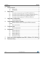
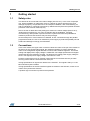
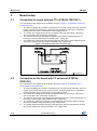
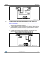
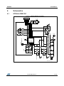
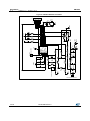
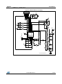
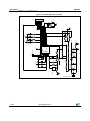
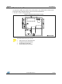
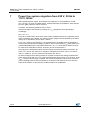
UM1082 User manual The STPM10 single-phase meter evaluation boards Introduction The STPM01 and STPM10 devices are energy meter ASSPs (application specific standard products), which address to a wide range of electricity metering requirements thanks to their built-in functions such as: signal conditioning, signal processing, data conversion, input/output signals, and voltage reference. The STPM10 is dedicated for peripheral use in microcontroller-based applications only, while the STPM01 works as a peripheral and as a standalone device, since it can permanently store configuration and calibration data. This user manual refers to the following STPM10 single-phase meter evaluation boards: STEVAL-IPE015V1: STPM10 single-phase meter with two CTs STEVAL-IPE016V1: STPM10 single-phase meter with CT and shunt STEVAL-IPE017V1: STPM10 single-phase meter with shunt STEVAL-IPE018V1: STPM10 single-phase meter with CT These metering modules can be used to build a Class 0.5 single-phase microprocessor-based meter, with or without tamper detection, for power line systems of VNOM=140 to 300 VRMS, INOM/IMAX=2/20 ARMS, fLIN=45 to 65 Hz and TAMB=-40 to +85 °C. The reading of the following documents is recommended: STPM10 datasheet AN2159 application note AN2299 application note UM1599 user manual UM1750 user manual October 2014 DocID18970 Rev 2 1/18 www.st.com Contents UM1082 Contents 1 2 3 Getting started ................................................................................. 3 1.1 Safety rules ....................................................................................... 3 1.2 Conventions ...................................................................................... 3 Board setup ..................................................................................... 4 2.1 Connection for board with two CTs (STEVAL-IPE015V1) ................. 4 2.2 Connection for the board with CT and shunt (STEVAL-IPE016V1)... 4 2.3 Connection for the board with shunt (STEVAL-IPE017V1) ............... 5 2.4 Connection for the board with CT (STEVAL-IPE018V1) ................... 6 Application configuration ............................................................... 7 3.1 4 Microprocessor-based ....................................................................... 7 Communication with the module ................................................... 8 4.1 Module evaluation with PC through the STPM1x evaluation software ......................................................................................................... 8 4.2 5 Technical data ............................................................................... 10 5.1 6 SPI communication ........................................................................... 9 Electrical parameters ...................................................................... 10 Schematics .................................................................................... 11 6.1 STEVAL-IPE015V1 ......................................................................... 11 6.2 STEVAL-IPE016V1 ......................................................................... 12 6.3 STEVAL-IPE017V1 ......................................................................... 13 6.4 STEVAL-IPE018V1 ......................................................................... 14 6.5 Mechanical outlines......................................................................... 15 7 Power line system migration from 220 V, 50 Hz to 110 V, 60 Hz 16 8 Revision history ............................................................................ 17 2/18 DocID18970 Rev 2 UM1082 Getting started 1 Getting started 1.1 Safety rules This board can be connected to the mains voltage (220 V/110 V). In the case of improper use, wrong installation or malfunction, there is a danger of serious personal injury and damage to property. All operations such as transport, installation, and commissioning, as well as maintenance, should be carried out by skilled technical personnel (national accident prevention rules must be observed) only. Due to the risk of death when this prototype is used on the mains voltage (220 V/110 V), “skilled technical personnel” only, who are familiar with the installation, mounting, commissioning, and operation of power electronic systems and have the qualifications needed to perform these functions may use this prototype. As the serial port P1 of the boards is not isolated, for PC connection through the parallel programmer/reader, the use of an isolated AC power supply to protect the parallel port and avoid board damage is strongly recommended. 1.2 Conventions In this user manual, the upper case is used to indicate the name of the pin of the module or the device or the corresponding signal; the underlined typeface is used to indicate the name of the configuration signal and italic is used to name software registers. The lowest analog and digital power supply voltage is called VSS. All voltage specifications for digital input/output pins are referred to as VSS. The highest OTP writing power supply voltage is VOTP. The highest power supply voltage of the device is VCC. Positive currents flow into a pin. Sinking means that the current flows into the pin while sourcing means that the current flows out of the pin. Timing specifications of signals are relative to the CLKOUT. This signal is fed by a 4.194 MHz onboard crystal oscillator. Timing specifications of the SPI interface signals are relative to the SCLNLC, which do not need to be in phase with CLKOUT. A positive logic convention is present in all equations. DocID18970 Rev 2 3/18 Board setup UM1082 2 Board setup 2.1 Connection for board with two CTs (STEVAL-IPE015V1) The connection of line signals to the module is shown in Figure 1: "Connection of two CTs to the power line": 1. 2. 3. 4. The hot line voltage wire must be connected to pin F of the module. Normally, this wire is also connected to the hot line current wire but, during the production or verification phases, this wire may be connected to a line voltage source. The neutral line voltage wire must be connected to pin N of the module. This wire is also connected to the neutral line current wire. The hot line current wire must pass through the hole of the current transformer Tr1 2 becoming a hot load wire using an isolated 4 mm copper wire. The neutral line current wire must pass through the hole of the current transformer Tr2 2 becoming a neutral load wire using an isolated 4 mm copper wire. Figure 1: Connection of two CTs to the power line 2.2 Connection for the board with CT and shunt (STEVALIPE016V1) The connection of line signals to the module is shown in Figure 2: "Connection of CT + shunt module to the power line": 1. 2. 3. 4. 5. 4/18 The hot line voltage wire must be connected to pin F of the module. Normally, this wire is also connected to the hot line current wire but, during the production or verification phases, this wire may be connected to a line voltage source. The neutral line voltage wire must be connected to pin N of the module. This wire is also connected to the neutral line current wire. The hot line current wire must be placed through the hole of the current transformer Tr 2 becoming a hot load wire using isolated 4 mm copper wire. The neutral line current wire must be connected to the pole of shunt which is close to 2 pin N of the module using an isolated 4 mm copper wire. The neutral load current wire must be connected to the pole of shunt which is close to 2 the current transformer using an isolated 4 mm copper wire. DocID18970 Rev 2 UM1082 Board setup Figure 2: Connection of CT + shunt module to the power line 2.3 Connection for the board with shunt (STEVAL-IPE017V1) The connection of line signals to the module is shown in Figure 3: "Connection of shunt module to the power line": 1. 2. 3. 4. The neutral line voltage wire must be connected to pin N of the module. This wire is also connected to the neutral line current wire. The hot line voltage wire must be connected to pin F of the module. Normally, this wire is also connected to the hot line current wire but, during the production or verification phases, this wire may be connected to a line voltage source. The neutral current wire must be connected to the pole of the shunt which is close to 2 pin N of the module using an isolated 4 mm copper wire. The neutral load current wire must be connected to the pole of the shunt which is 2 close to the edge of the module using an isolated 4 mm copper wire. Figure 3: Connection of shunt module to the power line DocID18970 Rev 2 5/18 Board setup 2.4 UM1082 Connection for the board with CT (STEVAL-IPE018V1) The connection of line signals to the module is shown in Figure 4: "Connection of CT module to the power line": 1. 2. 3. The hot line voltage wire must be connected to pin F of the module. Normally, this wire is also connected to the hot line current wire but, during the production or verification phases, this wire may be connected to a line voltage source. The neutral line voltage wire must be connected to pin N of the module. This wire is also connected to the neutral line current wire. The hot line current wire must pass through the hole of the current transformer Tr 2 becoming a hot load wire using an isolated 4 mm copper wire. Figure 4: Connection of CT module to the power line 6/18 DocID18970 Rev 2 UM1082 Application configuration 3 Application configuration 3.1 Microprocessor-based In this type of application, a control board with a microprocessor should be connected to the “male” P1 connector of the module using a 10-wire flat cable. Table 1: "Pin number, signal name and signal description of connector P1" below describes the signals corresponding to the pins of this connector. The four SPI signals are multipurpose pins and they actually reflect the functions of the corresponding pins on the onboard metering device. By using this type of connection, the control board is able to read data records or access configuration bits and mode signals of the metering device thanks to a dedicated protocol, it can draw up to 4 mA at +3.0 V from the module. Table 1: Pin number, signal name and signal description of connector P1 Pin Name Functional description of signal 1 Not used 2 Not used 3 GND Signal reference level 0 V and power supply return 4 SDA Digital I/O for SPI data signal or tamper indicator 5 SCS Digital for SPI enable signal 6 SCL Digital I/O for SPI clock signal or no load condition indicator 7 LED Device pulsed output 8 SYN Digital I/O for SPI data direction, latching request or negative power indicator 9 10 Not used VCC Power out of +5.0 V. Up to 25 mA can be drawn from this pin This kind of application may still use any LED element of the module for the purposes shown in Table 1: "Pin number, signal name and signal description of connector P1" or it may generate an alternative set of signals from the control board. In this case, the control board may also recalibrate any result read. DocID18970 Rev 2 7/18 Communication with the module UM1082 4 Communication with the module 4.1 Module evaluation with PC through the STPM1x evaluation software The metering module and the device features can be evaluated by a dedicated graphical user interface running on a PC. For this purpose, the module should be connected to the PC through a parallel programmer, shown in Figure 5: "Parallel programmer schematics" or to USB isolated hardware interface, available as a separate evaluation board with the code STEVALIPE023V1. Figure 5: Parallel programmer schematics To communicate with the device through the evaluation software, the selected hardware programmer has to be connected to both the PC and the evaluation board. Please take care that pin 1 of the cable is connected with the correct pin on the board, whose mark is printed on the PCB, close to the edge of the board. The correct connection for the STEVAL-IPE023V1 is shown in the picture below. 8/18 DocID18970 Rev 2 UM1082 Communication with the module Figure 6: Connection of the module to the STEVAL-IPE023V1 If the parallel interface is used, the evaluation board must be powered on. If the STEVALIPE023V1 is used, please make sure that jumper J4 is in 2-3 position, in this way it directly supplies the STPM10 evaluation board with 5 V. The evaluation software is available on http://www.st.com. 4.2 SPI communication A host system can communicate with the module using SPI signals and connect via the P1 connector. In fact, it communicates to the metering device, which is the key element of the module. This device always acts as an SPI slave while the host system acts as an SPI master. A control board of an application or an external system can be considered as a host. For details on SPI communication with the device please refer to the AN2159 and to the device datasheet. DocID18970 Rev 2 9/18 Technical data UM1082 5 Technical data 5.1 Electrical parameters Table 2: "Electrical parameters" summarizes the electrical parameters, which are specified for VCC = 3.6 V, TAMB = +25 °C, unless otherwise specified. Table 2: Electrical parameters Symbol Test conditions or comments Parameter Min. Typ. Max. Unit Nominal line voltage 140 220 300 VRMS Nominal frequency 45 50 55 Hz Target applications VNOM FL INOM Nominal line current 2 IMAX Maximal line current 20 30 ARMS TAMB Ambient temperature 25 85 °C 0.2 0.5 -40 Class of accuracy ARMS Digital inputs Valid also for I/O pins when they are used as inputs IIL Pull-up 15 µA VIL Voltage input low -0.3 0.25 VCC V VIH Voltage input high 0.75 VCC 5.3 V 0.4 V Digital outputs VOL Voltage output low IOL = +2 mA VOH Voltage output high IOH = +2 mA tTR Transition time CL = 50 pF, VCC = 3.2 V VCC-0.4 V 5 ns 0.1 VCC V Stepper outputs VOL Voltage output low IOL = +14 mA VOH Voltage output high IOH = +14 mA tTR Transition time CL=50 pF, VCC=5.0 V 0.9 VCC V 5 ns Power supply VCC Supply level ICC Quiescent current VDDA FL VCCPOR 10/18 3.165 5 5.5 V 4 5 6 mA Supply level 2.85 3 3.15 V Nominal frequency 45.0 50.0 65.0 Hz Power-on-reset 2.5 DocID18970 Rev 2 V DocID18970 Rev 2 mains 2 1 W1 W2 GNDA TR2 VDD 1uF R2 1k 1uF C3 L1 220uH 82 2W R27 D6 D7 DIODE 600V 1A + R9 L3 19 18 3 15 17 16 14 13 12 11 1uH 220K 5.1v D1 GND 4700µF 470nF 630v DIODE 600V 1A C4 C2 R8 220K R7 2M R20 2M R21 LED Sda WDG Scl ZCR U1 Scs Vddd Syn Vss CLKout Vcc CLKin Vdda Vin Vo STPM10 Vip Ilp1 Iln2 Iln1 Ilp2 220K R4 1k C10 4.7 4.7 10nF R22 R24 R3 1k R1 1k C9 4.7 4.7 10nF R23 R25 V1 1nF VARISTOR 300v 0R R18 Current transformer GNDA 0R R17 Current transformer TR1 1uF 20 1 2 4 5 6 8 7 9 10 GNDA GND VDD C11 22nF R19 43K R15 100 R5 390 R26 0R 4.194304MHz Y1 VDD GNDA 22pF GNDA C14 R16 1M GND 22pF C13 P1 1 2 3 4 5 6 7 8 9 10 STEVAL-IPE015V1 1nF C6 Vo SBS GND SDA SCS SCL LED SYN SBG 6.1 C8 D4 Schematics C7 TP1 D5. 1 2 2 2 R12 R11 R13 R14 2.4k 6.8K 6.8K 6.8K D2 1 6 C5 GNDA W5 W6 12 Stepper motor 1 1 2 D3 VDD GND UM1082 Schematics Figure 7: STEVAL-IPE015V1 schematic GIPG23102014825LM 11/18 12/18 DocID18970 Rev 2 W1 W2 2 1 mains 0R R18 SHUNT RS2 C9 10nF R27 R4 1k R3 1k 220K D6 220K C2 R8 2M R20 2M 220K R9 LED Sda WDG Scl ZCR U1 Scs Vddd Syn Vss CLKout Vcc CLKin Vdda Vin Vo STPM10 Vip Ilp1 Iln2 Iln1 Ilp2 R21 20 1 2 4 5 6 8 7 9 10 R7 10nF C10 R1 1k 4.7 4.7 R23 R25 R2 1k 1uF C6 TP1 19 18 3 15 17 16 14 13 12 11 GND L3 1uH C3 82 2W DIODE 600V 1A C4 D1 470nF 630v + V1 1nF D7 5.1v VARISTOR 300v DIODE 600V 1A 4700µF GNDA GNDA 0R R17 1uF C8 VDD L1 220uH 1uF 1nF Current Transformer TR1 C7 C5 GNDA 1 GND VDD 1 C11 22nF 6.8K D4 2 R14 1 R15 100 R5 390 R26 0R 6.8K D5. 2 R13 R19 43K 6.8K R11 D2 2 GNDA 2.4k 1 R12 D3 VDD 4.194304MHz Y1 VDD GNDA 22pF GNDA 22pF C14 R16 1M C13 GND SBS GND SDA SCS SCL LED SYN SBG VO P1 1 2 3 4 5 6 7 8 9 10 6.2 1 2 Stepper Motor W5 W6 2 GND Schematics UM1082 STEVAL-IPE016V1 Figure 8: STEVAL-IPE016V1 schematic GIPG231020140925LM DocID18970 Rev 2 GIPG231020140936LM 2 1 mains W1 W2 L1 220uH R27 R4 1k R3 1k C2 220K R7 10nF C10 R1 1k 10nF C9 R2 1k 1uF C6 D6 220K R8 2M 220K R9 19 LED Sda 18 WDG Scl 3 U1 ZCR Scs 15 Vddd Syn 17 Vss CLKout 16 Vcc CLKin 14 Vdda Vin 13 Vo STPM10 Vip 12 Ilp1 Iln2 11 Iln1 Ilp2 R21 20 1 2 4 5 6 8 7 9 10 TP1 GND GND VDD 6.8K 2.4k 1 6.8K R19 43K 22nF C11 R15 100 R5 390 6.8K D5. D4 2 2 R13 R14 R26 0R D2 2 R11 1 R12 GNDA C3 82 2W 470nF 630v DIODE 600V 1A D1 + V1 1nF D7 5.1v VARISTOR 300v DIODE 600V 1A 4700µF L3 1uH GNDA 0R R18 RS1 SHUNT 1uF 1nF 1uF VDD C8 C7 C5 GNDA 1 2 Stepper motor W5 W6 1 1 2 D3 VDD GNDA 22pF C14 GND GNDA 22pF R16 1M C13 4.194304MHz Y1 VO SBS GND SDA SCS SCL LED SYN SBG VDD P1 1 2 3 4 5 6 7 8 9 10 6.3 GND UM1082 Schematics STEVAL-IPE017V1 Figure 9: STEVAL-IPE017V1 schematic 13/18 14/18 DocID18970 Rev 2 2 1 mains W1 W2 GNDA GIPG231020141144LM 1nF 2M R21 + 220K R8 2M D7 TP1 19 18 3 15 17 16 14 13 12 11 L3 1uH 5.1v D1 GND 4700µF 220K R9 LED Sda WDG Scl ZCR U1 Scs Vddd Syn Vss CLKout Vcc CLKin Vdda Vin Vo STPM10 Vip Ilp1 Iln2 Iln1 Ilp2 R20 20 1 2 4 5 6 8 7 9 10 DIODE 600V 1A C4 D6 DIODE 600V 1A 470nF 630v C2 220K R7 10nF C10 R3 1k 82 2W C9 10nF R1 1k R4 1k R27 1uF C6 R2 1k 4.7 R25 1uF C8 VDD 4.7 R23 C3 L1 220uH 0R R18 V1 TR1 1uF 1nF VARISTOR 300v GNDA 0R R17 Current Transformer C7 C5 GNDA 1 2 Stepper motor W5 W6 GNDA GND VDD 6.8K 6.8K 2.4k R19 43K 1 6.8K R14 2 D4 22nF C11 R15 100 R5 390 R26 0R R13 2 D5. R11 2 D2 R12 1 1 1 2 D3 VDD GNDA 22pF C14 GND GNDA R16 1M 4.194304MHz Y1 22pF C13 Vo SBS GND SDA SCS SCL LED SYN SBG VDD P1 1 2 3 4 5 6 7 8 9 10 6.4 GND Schematics UM1082 STEVAL-IPE018V1 Figure 10: STEVAL-IPE018V1 schematic UM1082 6.5 Schematics Mechanical outlines The size of the PCB of the module can be seen below. The overall volume is determined by the size of the maximal element, which is the current transformer: L x W x H = 70 mm x 46 mm x 30 mm. Figure 11: Mechanical dimensions of PCB All measurements are given in mm View is from non-component side All high elements are dashed P1 has pins on both side All mounting holes are equal DocID18970 Rev 2 15/18 Power line system migration from 220 V, 50 Hz to 110 V, 60 Hz 7 UM1082 Power line system migration from 220 V, 50 Hz to 110 V, 60 Hz With capacitive power supply, the impedance of capacitor C1 and impedance of load ((VCC+0.7)/(ICC+IZ)) form a voltage divider. All other elements are needed for other reasons, such as: spike protection and HF rejection. Therefore, the following guidelines can be used. If the percentage of line frequency changes, the I CC changes the same percentage accordingly: df/f = d ICC / ICC For a 60 Hz system there is the 20% more current available because C1 impedance is the major component of the divider, the change of input voltage must be followed by the same change of C1 impedance, that is dU/U = dZc/Zc. For a 110 V system, the capacitor C1 is almost doubled, the divider must be designed to work properly at minimal line voltage, frequency and C1 and maximal I CC and therefore, the maximal allowable power consumption (500 mW > IZ * VCC) of the Zener diode D12 must be checked at maximal line voltage, frequency and C1 and minimal I CC. According to the information below, with the change of power line system from 220 V, 50 Hz to 110 V, 60 Hz, the value of C1 should be changed from 470 nF, 275 VAC to 750 nF, 150 VAC. A 680 nF, 150 VAC element means about 10% less ICC. No other change to the metering module is necessary because the voltage measurement range is from 20 to 360 VRMS. The current measurement range is from 0.1 to 20 ARMS, till 30 ARMS. If a wider current range is needed, the current transformers and the cross-section of primary winding wires must be increased, by running the risk that they do not fit onto the board of the module. In this case, the module needs to be recalibrated. 16/18 DocID18970 Rev 2 UM1082 8 Revision history Revision history Table 3: Document revision history Date Revision 13-Feb-2012 1 Initial release. 2 Updated Table 1: "Pin number, signal name and signal description of connector P1" and Table 2: "Electrical parameters". Updated Section 2.3: "Connection for the board with shunt (STEVAL-IPE017V1)" and Section 4.1: "Module evaluation with PC through the STPM1x evaluation software". Changed Figure 3: "Connection of shunt module to the power line". Minor text changes. 23-Oct-2014 Changes DocID18970 Rev 2 17/18 UM1082 IMPORTANT NOTICE – PLEASE READ CAREFULLY STMicroelectronics NV and its subsidiaries (“ST”) reserve the right to make changes, corrections, enhancements, modifications, and improvements to ST products and/or to this document at any time without notice. Purchasers should obtain the latest relevant information on ST products before placing orders. ST products are sold pursuant to ST’s terms and conditions of sale in place at the time of order acknowledgement. Purchasers are solely responsible for the choice, selection, and use of ST products and ST assumes no liability for application assistance or the design of Purchasers’ products. No license, express or implied, to any intellectual property right is granted by ST herein. Resale of ST products with provisions different from the information set forth herein shall void any warranty granted by ST for such product. ST and the ST logo are trademarks of ST. All other product or service names are the property of their respective owners. Information in this document supersedes and replaces information previously supplied in any prior versions of this document. © 2014 STMicroelectronics – All rights reserved 18/18 DocID18970 Rev 2